low-power high-speed low-offset fully dynamic cmos latched ...1279/... · low -power high-speed low...
TRANSCRIPT

1
LOW -POWER HIGH-SPEED LOW -OFFSET
FULLY DYNAMIC CMOS LATCHED COMPARATOR
A Thesis Presented
by
HeungJun Jeon
to
The Department of Electrical and Computer Engineering
in partial fulfillment of the requirements for the degree of
Master of Science
in
Electrical Engineering
Northeastern University
Boston, Massachusetts
May, 2010

2
April, 2010
NORTHEASTERN UNIVERSITY
Graduate School of Engineering
Thesis Title: LOW-POWER HIGH-SPEED LOW-OFFSET FULLY DYNAMIC CMOS LATCHED COMPARATOR
Author: HeungJun Jeon
Department: Electrical and Computer Engineering
Approved for Thesis Requirement of the Master of Science Degree
Thesis Adviser, Dr. Yong-Bin Kim Date
Thesis Reader, Dr. Fabrizio Lombardi Date
Thesis Reader, Dr. Gunar Schirner Date
Department Chair, Dr. Ali Abur Date
Graduate School Notified of Acceptance: Director of the Graduate School, Dean Yaman Yener Date

3
ABSTRACT
A new fully dynamic latched comparator which shows lower offset voltage and higher
load drivability than the conventional dynamic latched comparators has been designed. With
two additional inverters inserted between the input- and output-stage of the conventional
double-tail dynamic comparator, the gain preceding the regenerative latch stage was
improved and the complementary version of the output-latch stage, which has bigger output
drive current capability at the same area, was implemented. As a result, the circuit shows up
to 19% less offset voltage and 62% less sensitivity of the delay versus the input voltage
difference (delay/log(∆Vin)), which is about 17ps/decade, than the conventional double-tail
latched comparators at approximately the same area and power consumption. Along with the
proposed design, this thesis provides a comprehensive review about a variety of traditional
dynamic latched comparator designs - in terms of performance, power, area and input-
referred offset voltage.

4
ACKNOWLEDGEMENTS
I would like to thank my advisors, Dr. Yong-Bin Kim for his continuous guidance and
encouragement. Besides, Dr. Kim, I would like to thank my thesis committee, Dr. Fabrizio
Lombardi and Dr. Gunar Schirner. Lastly, I would like to thank my parents who gave me
encouragement and support all the way.

5
TABLE OF CONTENTS
Abstract ........................................................................................................................ 3
Acknowledgements ...................................................................................................... 4
Table of Contents ......................................................................................................... 5
List of Figures and Tables ............................................................................................ 7
Chapter 1: Introduction ........................................................................................... 8
1.1 Motivation ....................................................................................................... 8
1.2 Thesis Organization ...................................................................................... 10
Chapter 2: Literature Review ................................................................................ 11
2.1 Design Considerations for Voltage Comparator ......................................... 11
2.2 Comparator Architectures ........................................................................... 13
2.2.1 Open-Loop Comparators ............................................................................ 13
2.2.2 Pre-amplifier Based Latched Comparators ................................................. 14
2.2.3 Fully Dynamic Latched Comparators ......................................................... 16
A. Resistor Divider (Lewis-Gray) Comparator ....................................... 16
B. Differential Pair Comparator (Latch-Type Voltage SA) .................. 19
C. Double-Tail Dynamic Latched Comparators ..................................... 21
Chapter 3: Proposed Dynamic Latched Comparator ............................................ 25
3.1 Operation Principles of Proposed Comparator ................................................... 25
3.2 Offset Voltage Analysis for Proposed Comparator .......................................... 28
3.2.1 Dynamic Differential Input Gain-Stage ...................................................... 28
3.2.2 Output Latch-Stage ..................................................................................... 33
3.2.3 Simulation Results for Output Latch-Stage Offset Voltage ....................... 37

6
Chapter 4: Simulation Results .............................................................................. 39
Chapter 5: Conclusion and Future Work .............................................................. 42
5.1 Conclusion .................................................................................................... 42
5.2 Future Work .................................................................................................. 42
References .................................................................................................................. 43
Appendix A: 90nm PTM Model File ............................................................................. 46
Appendix B: HSPICE Netlist Files for Simulated Comparator Circuits ....................... 49

7
L IST OF FIGURES AND TABLES
Figure 1 Typical block diagram of a high-speed voltage comparator
Figure 2 Comparator (a) Circuit symbol, (b) Ideal voltage transfer curve, and (c) Practical voltage transfer curve including finite gain, offset voltage and RMS noise [8].
Figure 3 (a) Two-stage open-loop comparator (b) Push-pull output open-loop comparator (lower gain but able to sink/source large amount of current in the output capacitance)
Figure 4 (a) A static latched comparator (b) A class-AB latched comparator
Figure 5 (a) Lewis-Gray Comparator (Resistor Divider Comparator) (b) Simplified form of resistor divider comparator (will be referred as Comparator 1)
Figure 6 (a) Differential pair comparator [24, 25] (b) Latch-type voltage SA (sense amplifier) [1], [2] (will be referred as Comparator 2)
Figure 7 (a) Double-tail latch-type voltage SA [3] (Comparator 3) (b) Energy efficient two-stage comparator [26] (Comparator 4)
Figure 8 Two-stage Dynamic comparator (without offset calibration) [4] (Comparator 5)
Figure 9 (a) Schematic of proposed comparator; (b) Signal behavior of proposed comparator (∆V in=100mV (Grey), 10mV (Black) with VDD=1V, fclk=3GHz, Cload=7fF, Temp.=25oC and Vcom=0.7V)
Figure 10 Simplified schematic of the dynamic differential input gain stage. (The time point from the tail transistor M1 is just turning on at the rising Clk edge during evaluation phase.)
Figure 11 Simplified schematic of the output stage combined with latch when Di’ node voltages (VDi’ ) are reaching around Vtn12,13 during evaluation phase.
Figure 12 Simulated delay (ps) versus ∆Vin=|Vin+–Vin-| [V] for selected multi-stage dynamic comparators with different load capacitances of 7fF and 10fF (VDD=1V, Vcom=0.7V, fclk=3GHz and Temp.=25oC).
Table 1 Offset Voltages from Mismatch Critical Pairs
Table 2 Performance Comparison
8
Chapter 1
Introduction
1.1 Motivation
Due to fast-speed, low-power consumption, high-input impedance and full-swing
output, CMOS dynamic latched comparators are very attractive for many applications such as
high-speed analog-to-digital converters (ADCs), memory sense amplifiers (SAs) and data
receivers. They use positive feedback mechanism with one pair of back-to-back cross
coupled inverters (latch) in order to convert a small input-voltage difference to a full-scale
digital level in a short time. However, an input-referred latch offset voltage (hence offset
voltage), resulting from the device mismatches such as threshold voltage Vth, current factor β
(=µCoxW/L) and parasitic node capacitance and output load capacitance mismatches, limits
the accuracy of such comparators [5], [6]. Because of this reason, the input-referred latch
offset voltage is one of the most important design parameters of the latched comparator. If
large devices are used for the latching stage, a less mismatch can be achieved at the cost both
of the increased delay (due to slowing the regeneration time) and the increased power
dissipation.
More practically, the input-referred latch offset voltage can be reduced by using the
pre-amplifier preceding the regenerative output-latch stage as shown in Figure 1. It can
amplify a small input voltage difference to a large enough voltage to overcome the latch
offset voltage and also can reduce the kickback noise [11]. However, the pre-amplifier based
comparators suffer not only from large static power consumption for a large bandwidth but

9
also from the reduced intrinsic gain with a reduction of the drain-to-source resistance rds due
to the continuous technology scaling [7].
In the literature, various kinds of CMOS comparators can be found. The types of the
comparators can be classified largely into three: Open-loop Comparators (op-amps without
compensation), Pre-amplifier Based Latched Comparators (open-loop comparator combined
with dynamic regenerative latch), and Fully Dynamic Latched Comparator. In this paper,
various kinds of fully dynamic latched comparators will be fully analyzed in terms of their
advantages and disadvantages along with operating principles and experimental results of the
speed, power consumption, and offset voltage at a limited area. Then, a new dynamic latched
comparator which shows lower offset voltage and higher load drivability than the
conventional dynamic latched comparators is proposed.
Figure 1 Typical block diagram of a high-speed voltage comparator

10
1.2 Thesis Organization
This thesis provides a new dynamic latched comparator which shows lower offset voltage
and higher load drivability than the conventional dynamic latched comparators. The
remaining parts of the thesis are organized as follows. Chapter 2 reviews the important
features (design considerations) of voltage comparators, introduces and classifies popular
structures of voltage comparators. Chapter 3 explains the operation principles of each
structure and compares them in terms of speed, power consumption, offset voltage and area.
Chapter 4 presents the proposed fully dynamic latched comparator and conclusion and future
works are drawn in Chapter 5. The used 90 nm PTM (Predictive Technology Model) files
and HSPICE netlist files for each comparator circuit are attached in the Appendix.

11
Chapter 2
Literature Review
In this chapter, important features and design considerations of a voltage comparator will be
reviewed. In addition, a different kind of comparator architectures will be reviewed after
classifying them into three: Open-loop Comparator, Pre-amplifier Based Latched
comparator, and Fully Dynamic Latched Comparator. Especially, fully dynamic latched
comparators will be analyzed in detail.
2.1 Design Considerations for Voltage Comparator
The basic function of a comparator is to compare an analog signal with another analog
signal or reference and output a binary signal based on comparison. Since it is easier to
distribute voltages to a large number of comparators than to distribute currents, most
converters employ voltage comparison [9]. A voltage comparator can be simply regarded as a
1-bit ADC.
The circuit symbol and ideal and practical voltage transfer functions of a comparator
are shown in Figure 2. As shown in Figure 2 (b), the ideal comparator outputs VOH (logic
high “1” = VDD) if Vin+ − Vin− > 0 and else it outputs VOL (logic low “0” = 0V (or –VSS))
since it has infinite gain, zero offset voltage and zero RMS noise. However, for a practical
comparator shown in Figure 2 (c), it outputs VOH only if Vin+ − Vin− > VIH + VOS (+ |Vnoise|)
and it outputs VOL only if Vin+ − Vin− < VIL (− |Vnoise|) because it has a finite gain (�� ��������������� , non-zero offset voltage and RMS noise (for latched comparators, VIL and VIH are
limited by its sampling (or Clk) frequency due to meta-stability.)

12
Therefore, design considerations for voltage comparators are can be summarized as
high-speed (maximum clock rate fs, which is related to small signal bandwidth, slew rate, and
settling time), accuracy (high-resolution, which is related to gain, offset voltage [27], [29],
[34] RMS and kickback noise [11], [32], [33], overdrive recovery, and linearity of input
capacitance), wide input common–mode range, CMR (common-mode rejection), low-power
consumption, small-area and so on [35]. In the next section, architectures of voltage
comparators will be classified in to into three: Open-loop Comparators (op-amps without
compensation), Pre-amplifier Based Latched Comparators (open-loop comparator combined
with dynamic regenerative latch), and Fully Dynamic Latched Comparator and will be
reviewed in terms of their advantages and disadvantages.
Figure 2 Comparator (a) Circuit symbol, (b) Ideal voltage transfer curve, and (c) Practical
voltage transfer curve with finite gain, offset voltage and RMS noise [8].

13
Figure 3 (a) Two-stage open-loop comparator (b) Push-pull output open-loop comparator
(lower gain but able to sink/source large amount of current in the output capacitance)
2.2 Comparator Architectures
2.2.1 Open-Loop Comparators [8], [30], [31]
Open-loop, continuous time comparators, shown in Figure 3 [8], are an operational
amplifier without frequency compensation to obtain the largest possible bandwidth, hence
improving its time response. Since the precise gain and linearity are of no interest in
comparator design, no-compensation does not pose a problem. However, due to its limited
gain-bandwidth product, open-loop comparators are too slow for many applications. One the
other hand, a cascade of open-loop amplifiers usually has a significantly larger gain-
bandwidth product than a single-stage amplifier with the same gain. However, since it costs
more area and power consumption, cascading does not give practical advantages for many
applications.

14
2.2.2 Pre-amplifier Based Latched Comparators
Figure 4 shows typical types of pre-amplifier based latched comparators [11]. The
main advantages of the pre-amplifier based latched comparators are their fast speed and low
input referred latch offset voltage. Typically, pre-amplifier, which consists of one or two
stages of an open-loop comparator, has a gain of 4 - 10 V/V and it can reduce the input-
referred latch offset voltage by its gain. For example, if a pre-amplifier has gain of 10 V/V
and a latch stage has an offset voltage of 50mV, then the input-referred latch offset voltage
will be 5 mV. In addition, by using pre-amplification stage, kickback noise [11] can be
considerably reduced (by isolation between the drains of the differential pair transistors and
the regeneration nodes) and meta-stability problem also can be relaxed.
Latched comparators commonly employ one or two clock signals (Clk and Clkb) to
determine the modes of operation: Track Mode (Reset): output is reset and input is tracked,
Latch Mode (Evaluation): output is toggled by using a positive feedback. For the operation of
the circuit shown in Figure 4 (a) [12-17], during reset phase (Clkb=0V), both complementary
output Vout+ and Vout− are reset to 0V by reset (switch) transistor M10 and M11. During
Figure 4 (a) A static latched comparator (b) A class-AB latched comparator

15
evaluation phase (Clkb=VDD), as the reset transistors are off, the comparison will be
performed by a positive feedback from transistor M7 and M9. While this comparator present
low kickback noise, relatively large static power consumption and slow regeneration due to
its limited current operation make it less attractive [11]. Similarly, the operation for the
circuit shown in Figure 4 (b) [18-22], during reset phase (Clk=0V), PMOS reset transistor
M7 will be shorted and make both outputs equal: Vout+ = Vout− while NMOS transistor M8 is
off. During evaluation phase (Clk=VDD), as the reset transistor M7 is off and the tail transistor
of the latch M8 is on, the comparison will be made by a positive feedback formed from back-
to-back cross coupled inverter pairs (M4/M6 and M5/M7). While this comparator shows
faster speed and consumes less power, it generates more kickback noise and during reset
phase both outputs (Vout+, Vout−) are not reset exactly to either VDD or 0V [11].
It can be concluded that pre-amplifier based latched comparators, which is a
combination of a pre-amplifier and a latch, offer fast speed and low offset while they still
consume static power.

16
2.2.3 Fully Dynamic Latched Comparators
A. Resistor Divider Comparator (or Lewis-Gray Comparator)
The comparator shown in Figure 5 (a) was introduced in [23]. Since the input
transistor M1A/B and M2A/B operate in the triode region and act like voltage controlled
resistors, this comparator is called “Resistive Divider Comparator.” The advantage of this
comparator is its low power consumption (No DC power consumption) and adjustable
threshold voltage (decision level) which is defined as
�� ��������� � ������ ��� 1
���� �� � �!� � �"� �� � �!� � �"�
�� � ��# $ ��� ��� � ���# $ ����
Figure 5 (a) Lewis-Gray Comparator (Resistor Divider Comparator) (b) Simplified form of
resistor divider comparator (will be referred as Comparator 1)

17
For the analysis, the simpler form of the comparator shown in Figure 5 (b) will be
used. During reset phase (Clk=0V), PMOS reset transistor M9 and M10 charge Out nodes up
to VDD (this makes NMOS transistor M3 and M4 on and the node voltage at VD3,4 discharge to
ground) and input transistor M1 and M2 discharge Di nodes to ground while NMOS
transistor M5 and M6 are off. During evaluation phase (Clk=VDD), as both switch transistor
M5 and M6 are on, each node voltage at Di+ and Di− instantly rises up to the certain values,
which are defined as %�# � �&'! (��&'! (� ) �&'*,, (� ) �&'-,. (� / (01� 2 %% 2 %�� � �&'" (��&'" (� ) �&'*,, (� ) �&'-,. (� / (01# 2 %% 3
Then, each Out node voltage starts to discharge from VDD to ground inversely proportional to
the applied input voltage such a way; Vin+↑ → VDi↓ → VGS3↑ → ID3↑ → Vout-↓ → VGS4↓ →
Vout+↑ (→VGS3↑…). With positive feedback operation from the back-to-back cross-coupled
inverter pairs (M7/M3 and M8/M4), one Out node will discharge to ground and the other Out
node will charge up to VDD again and this comparator will finish its comparison. Since the
input transistor M1 and M2 are operated in the linear region during evaluation phase, the
transconductance for those transistors are can be approximately written as
56!," � 7�8(9 ��!,": � &'!," 4
Also, because transistor M3 and M4 are operated in the saturation region during evaluation
phase, the transconductance for those transistors are can be written as

18
56*,, � 7�8(9 ��*,,: � <'*,, $ 1� 5
The transconductance of transistor M3 and M4 is much larger than that of the input
transistor pair; hence the differential voltage gain built between Di nodes from the input
transistor pair is not big enough to overcome an offset voltage caused from such a small
mismatch between transistor M3 and M4 pair. As a result, those transistors are the most
critical mismatch pair in this comparator and needed to be sized big enough to minimize the
offset voltage at the cost of the increased power consumption. Besides, the mismatch between
transistor M5 and M6 pair (which is switches and operated in the linear region) also causes
the considerable input-referred offset voltage. Furthermore, as the common mode voltage
Vcom of the input transistor pair increases, the relative difference between the voltage
controlled resistors (rds1,2) becomes smaller at the same amount of the input voltage
difference ∆Vin and this in turn increases the offset voltage.
It can be concluded that despite its advantages such as zero-static power consumption
and adjustable threshold voltage, since Lewis-Gray comparator shows a high offset voltage
and its high offset voltage dependency on a different common mode voltage Vcom, it is only
suitable for low resolution comparison.

19
B. Differential Pair Comparator/Latch-type Voltage SA
The comparator shown in Figure 6 (a) was first proposed in [24] (without extra
switching transistor M10 and M11 shown in grey-colored.) Similar to Resistive Divider
Comparator, this comparator also has an adjustable threshold voltage and it can be defines as
�� ��������� � > · ��� 6
���� 2�>"A%!� ���: � $ 7�8(9>,���" ���: �" � 2A%. ���: � $ 7�8(9���" ���: �"
�� � ��# $ ��� ��� � ���# $ ���� A!� � � · A!�
For the analysis, the simpler form of the comparator shown in Figure 6 (b) will be
used and extra switching transistor M10 and M11 are added to improve its characteristics;
since those additional PMOS switch transistors increase the time the input transistor pair M2
and M3 being operated in the saturation region during evaluation phase (Clk=VDD), hence the
amplification from the differential input pair increases.
Figure 6 (a) Differential pair comparator [24, 25] (b) Latch-type voltage SA (sense
amplifier) [1], [2] (will be referred as Comparator 2)

20
The operation of the comparator can be simply described as follows. During reset
phase (Clk=0V), Out nodes of the cross-coupled inverters (M6-M9) are reset to VDD through
the reset transistors M4 and M5. During evaluation phase (Clk=VDD), the tail transistor M1 is
turned on at the rising Clk edge. The input transistor pair (M2 and M3) starts to discharge
each Di node voltage with a different time rate proportional to the each applied input voltage
from VDD to 0V. Once either of Di node voltages drops around VDD−Vtn, then the NMOS
transistors of the cross-coupled inverters M6 and M7 turn on and this initiates the positive
feedback. Once either of Out node voltage reaches around VDD−|Vtp|, the PMOS transistors of
the inverters M2 and M4 also turn on; further enhancing the positive feedback and enabling
the regeneration of a small differential voltage ∆Vin to a full swing differential output.
Comparing with Lewis-Gray comparator, this comparator shows faster operation and
less overall offset voltage. However, still its structure which consists of a stack of 4
transistors requires large voltage headroom; it is problematic in low-voltage deep-submicron
CMOS technologies. Furthermore, in order to increase the drive currents of the latch, it is
inevitable to size up the transistor M1 since this comparator has only one tail transistor M1. If
the size of transistor M1 is increased, the drain currents of both input transistors M2 and M3
will increase during evaluation phase (Clk=VDD). This, in turn, means the reduction of the
time duration for transistor M2 and M3 being operated in saturation region because Di nodes
discharge from VDD to ground in a very short period. Consequently, lower amplification of
the input voltage difference will be made and such a small Vth variation from mismatch
between transistor M6 and M7 can yield high input-referred offset. In addition, since it shows
the strong dependency on speed and offset voltage with a different common-mode input
voltage Vcom [2], it is less attractive in applications with wide common-mode ranges such as
ADCs [3].

21
C. Double-Tail Dynamic Latched Comparators
To mitigate the drawbacks (strong dependency on speed and offset with a different
common-mode input voltage Vcom and problem in low power supply voltage operation due to
its structure: a stack of four transistors) from the comparator shown in Figure 6 (b), a
comparator with separated input-gain stage and output-latch stage, shown in Figure 7 (a),
was first introduced in [3]. This separation made this comparator have a lower and more
stable offset voltage over wide common-mode voltage (Vcom) ranges and operate at a lower
supply voltage (VDD) as well. It is because by controlling the sizes of the tail transistors (M1
and M12) of the input- and output-stage such a way that a small tail current for the
differential input pair to obtain a long integration time and a better gm/ID2,3 ratio for a bigger
gain (hence, less offset voltage) and a large tail current for the output latch-stage for fast
regeneration, one can get fast speed and low offset voltage with less dependence on Vcom.
Figure 7 (a) Double-tail latch-type voltage SA [3] (Comparator 3) (b) Energy efficient two-
stage comparator [26] (Comparator 4)

22
For its operation, during reset phase (Clk=0V, Clkb=VDD), PMOS transistor pair M4
and M5 pre-charge Di node capacitances up to VDD (sequentially, the input transistor pair for
the output stage M10 and M11 are turned on and Out nodes are reset to 0V) while the both
tail transistors (M1 and M12) in the input stage and output latch-stage are off. During
evaluation phase (Clk=VDD, Clkb=0V), once the input-stage tail transistor M1 is turned on,
each Di node voltage starts to discharge from VDD to ground with a different time rate
proportional to each input voltage. Then, the voltage difference built between Di nodes is
passed to Out nodes in the output latch-stage through the input transistor pair (M10 and M11)
of the output latch-stage. The cross-coupled inverters start to regenerate the voltage
difference formed between Out nodes as soon as the common-mode voltage at the Di nodes is
not big enough to clamp Out nodes to ground and the PMOS output tail transistor M12 is on.
As expected, since this comparator requires both Clk and Clkb signals for its operation,
high accuracy timing between Clk and Clkb is required because the second stage has to detect
the voltage difference between the differential outputs of the first gain stage at very limited
time. If a simple inverter replaces Clkb, Clk has to be able to drive an additional large inverter
(heavier clock load) in order to drive the largest transistor M12 in a small delay. If Clkb is
lagging Clk, it results in increased delay and if Clkb is leading Clk, it results in increased
power dissipation due to existing the short circuit current path M12 to M10/M11 though
M8/M9 and it can even increase the latch offset voltage if the device mismatch between M8
and M9 is significant.
The comparator shown in Figure 7 (b) is a different version of two-stage dynamic
latched comparator. The operation is similar to the comparator shown in Figure 7 (a). By
modifying the output latch-stage, during reset phase (Clk=0V, Clkb=VDD), its Di node
capacitances, mostly drain diffusion capacitances of PMOS transistor (M10 and M11) and
NMOS transistors (M2 and M3), are reduced, which is much less than the Di node

23
capacitances, mostly gate capacitances of NMOS transistor M10 and M11, in the comparator
in [3]; therefore, it can be operated at less power consumption and faster speed. However,
since it still has Clk and Clkb for its operation, high accuracy timing between Clk and Clkb is
required and due to reduced Di node capacitances the relative capacitance mismatch ∆CDi/CDi
and the input referred RMS noise are also increased.
The comparator from [4] without offset calibration technique, shown in Figure 8,
resolved the problem by replacing Clkb with Di nodes. As a result, Clk load was lessened and
the input-referred offset was reduced because the output latch-stage obtains the gain from the
both second-input transistor pairs (M10/M11 and M12/M13). However, the improved offset
has to trade off with the increased delay since the current drivability of the output load was
Figure 8 Two-stage Dynamic comparator (without offset calibration) [4] (Comparator 5)

24
weakened due to the fact that transistor M12 and M13 use Di node voltages as their Clkb
signal, which show slow exponential decay shape, and that the maximum drive current of
each Out node was reduced to half of the single output tail current of M12 comparing with
Comparator 1 since it was separated into two transistors M12 and M13.

25
Chapter 3
Proposed Dynamic Latched Comparator
3.1 Operation Principles of Proposed Comparator
Figure 9 (a) Schematic of proposed comparator; (b) Signal behavior of proposed
comparator (∆V in=100mV (Grey), 10mV (Black) with VDD=1V, fclk=3GHz, Cload=7fF,
Temp.=25oC and Vcom=0.7V)

26
The schematic and simulated waveforms of the proposed comparator are shown in
Figure 9. The circuit is designed and simulated with HSPICE using 90nm PTM (Predictive
technology Model) [28], and the design and simulation conditions are VDD=1V, fclk=3GHz,
Cload=7fF, Temp.=25oC, and common mode voltage Vcom=0.7V. The basic structure of the
proposed comparator stems from the comparators from [3] and [4]. Therefore, the proposed
comparator provides better input offset characteristic and faster operation in addition to the
advantages of those comparators such as less kickback noise, reduced clock load and removal
of the timing requirement between Clk and Clkb over a wide common-mode and supply
voltage range.
For its operation, during the pre-charge (or reset) phase (Clk=0V), both PMOS
transistor M4 and M5 are turned on and they charge Di nodes’ capacitance to VDD, which turn
both NMOS transistor M16 and M17 of the inverter pair on and Di’ nodes discharge to ground.
Sequentially, PMOS transistor M10, M11, M14 and M15 are turned on and they make Out
nodes and Sw nodes to be charged to VDD while both NMOS transistors M12 and M13 are
being off.
During the evaluation (decision-making) phase (Clk=VDD), each Di node capacitance
is discharged from VDD to ground in a different time rate in proportion to the magnitude of
each input voltage. As a result, an input dependent differential voltage is formed between
Di+ and Di- node. Once either Di+ or Di- node voltage drops down below around VDD - |Vtp|,
the additional inverter pairs M18/M16 and M19/M17 invert each Di node signal into the
regenerated (amplified) Di’ node signal. Then the regenerated and different phased Di’ node
voltages are amplified again and relayed to the output-latch stage by transistor M10−M13. As
the regenerated each Di’ node voltage is rising from 0V to VDD with a different time interval
(or a phase difference, which increases with the increasing input voltage difference ∆Vin),
M12 and M13 turn on one after another and the output-latch stage starts to regenerate the

27
small voltage difference transmitted from Di’ nodes into a full-scale digital level: Out+ node
will output logic high (VDD) if the voltage difference at Di’ nodes ∆Di’(t) is negative (Di+’(t)
< Di-’(t) ) and Out+ will be low (0V) otherwise. Once either of the Out node voltages drops
below around VDD - |Vtp|, this positive feedback becomes stronger because either PMOS
transistor M8 or M9 will turn on.

28
3.2 Offset Voltage Analysis for Proposed Comparator
3.2.1 Dynamic Differential Input Gain-Stage
The simplified first stage of the proposed comparator is show in Figure 10. During
evaluation phase (Clk=VDD), the input differential pair discharges each Di node voltage from
VDD down to 0V with a different time rate proportional to each input voltage. By assuming
that λ = γ = 0 for simplicity, since both transistor M2 and M3 operate in the saturation region
between the time t1 and t2 (t1: time at which transistor M1 is just turned on at the rising Clk
edge and transistor M2 and M3 start to operate in the saturation region, t2: time at which
either of transistor M2 or M3 moves out of the saturation region operation and goes into the
linear region operation), the drain-to-source current of M2 and M3 are constant over [t1, t2].
Therefore, the currents can be expressed as
Figure 10 Simplified schematic of the dynamic differential input gain stage. (The time point
from the tail transistor M1 is just turning on at the rising Clk edge during evaluation phase.)

29
8%�� �%�� ��� � BCDEF � � $A%" 7
8%�# �%�# ��� � BCDEH � � $A%* 8
By integrating both sides of (7) and (8) over [t1, t] and applying the initial condition:
VDi(t1)=VDD, the following equations are obtained;
%�� � � %% $ A%"8%�� � %�# � � %% $ A%*8%�# � 9
∆%� � � %�� � $ %�# � 10
Then, under the assumption that ∆Vin (= Vin+ − Vin-) is constant over the integration time [t1, t]
(t is between t1 and t2), the dynamic gain of the first stage can be defined as
��! � � ∆%� �∆�� 11
By applying the small signal approximation: 2(VGS2,3 – Vtn) >>∆Vin and assuming that CDi- =
CDi+ = CDi, Equation (11) can be expressed as
��! � � $ 56",*8%� � 12
���� 56",* � 7�8(9 ",*: M(6 $ %! � $ 1�",*
%! � � A%" ) A%* · �&'! 2 8�N��. Equation (12) reveals that as long as the input transistor pair M2 and M3 operates in the
saturation region and ∆Vin does not change over [t1, t2], the dynamic gain AV1(t) keeps
increasing with the increasing time. To maximize the gain |AV1(t)|, |gm2,3/ID2,3| should be
maximized because the integration time t is proportional to CDi/ID2,3 from (9). Simply, this

30
can be done with reducing the size of transistor M1. However, as equation (9) also indicates,
the reduced ID2,3 increases the discharging time of Di node voltages during evaluation phase.
Therefore, the higher gain can be achieved at the cost of the increased delay.
Furthermore, by increasing the channel length of the input transistor, for example
90nm to 120nm in 90nm technology, one can get higher gain with the same W2,3/L ratio by
reducing short-channel effects such as a dynamic conductance variation due to DIBL. If a
negative supply voltage is available, by replacing the ground of the input differential pair
with a negative supply voltage and further reducing the size of transistor M1, one can get
wider common mode input range. Therefore, this differential input stage can be designed in a
different way depending on the requirements such as the speed, offset voltage and common
mode input voltage range.
To calculate the offset voltage (VOS, pre1) of the input differential pair, both input
transistors and Di node capacitances are assumed to be mismatched. Then, the device
parameters and Di node capacitances can be express as;
�7�8(9 �: �" � P �7�8(9 �: �* � P ) ∆P
1�" � 1� 1�* � 1� ) ∆1� 13
8%�� � 8 8%�# � 8 ) ∆8
Then, the value ∆Vin(=Vin+− Vin−) which make ∆VDi = 0 is the offset voltage (VOS,pre1),
which is equal to VGS2 − VGS3. From equation (9), (10) and ∆VDi = 0, it can be derived that
ID2 CDi+ = ID3 CDi− . Since we assumed that Di node capacitances were mismatched (CDi+ ≠
CDi−), ID2 cannot be equal to ID3. By assuming that ID2 = ID and ID3 =I D +∆ID, ∆ID/ID = ∆C/C is
obtained. Therefore, the offset voltage is derived by following way [9].
QR,S��! � QR",* � TR" $ TR* 14

31
QR,S��! � U 2A%"P" ) 1�" $ U 2A%*P* $ 1�* 15
� U 2A%P VWWWX 1 $ Y 1 ) ∆A%A%1 ) ∆PP Z[[
[\ $ ∆1� 16
]^�� > _ 1, √1 ) > 2 1 ) >2 aN� b√1 ) > c�! 2 1 $ >2 d
Assuming ∆ID/ID << 1 and ∆β/β << 1, equation (16) is reduced to
QR,S��! � U 2A%P e 1 $ �1 ) ∆A%2A%� �1 $ ∆P2P� f $ ∆1� 17
� U A%2P e$ ∆A%A% ) ∆PP f $ ∆1� 18
� TR",* $ 1�2 e $ ∆88 ) ∆PP f $ ∆1� 19
Considering the charge injection mismatch (∆Q) between PMOS switch transistor M4 and
M5, the additional term ∆Q/CDi has to be added to equation (19). Since mismatches are
independent statistical variables, the random offset voltage (VOS,pre1) can be expressed as the
variance of (19)
QR,S��! " � ∆1�" ) �TR",* $ 1�2 �" g�∆8%�8%� �" ) �∆PP �"h ) �∆i8%��" 20
Equation (20) shows that (1) the threshold voltage mismatch is directly referred to the input,
(2) Di node capacitance mismatch (which consists of the mismatch between the gate

32
capacitances of inverter pair (M18/M16 and M19/M17) and the mismatch between the drain
diffusion capacitances of the input transistor pair (M2 and M3)) and the current factor β
mismatch increases with the increasing common mode voltage Vcom, and (3) the influence of
the charge injection mismatch (∆Q) on the offset voltage is related to Di node capacitance [9],
[28]. Since all terms are related to the size of transistors, from (29) and (30) in Section 3.2.3,
the offset voltage can be reduced at the cost of the increasing size of the transistors, hence
increasing area and power consumption.

33
3.2.2 Output Latch-Stage
The inputs of the output latch stage are the gates of transistor M10-13 which are
connected to Di−’ and Di+’ nodes. During evaluation phase (Clk = VDD), if Vin+ ≠ Vin−, each
Di’ node voltage rises from 0V to VDD with a different time interval. Thus, the output stage
can make a decision whether logic high or low. However, if Vin+ = Vin− and no mismatch
exists, both Di’ node voltages rise up exactly at the same time rate. This makes both branches
of the output stage maintain in a balanced state, which means Vout+(t) = Vout−(t) during all the
transient time.
However, if a mismatch exits in the output latch stage, the circuit will be unbalanced
making Vout+(t) ≠ Vout−(t). In order for the circuit to be balanced, a voltage VOS, latch should be
applied between the output of the inverter (M18/M16) and Di-’ node to compensate the
mismatch when Di’ nodes rises. In order to calculate the offset voltage VOS, latch of the output
stage, the mismatch in current factor β and threshold voltage Vth are assumed to be the
dominant factors to cause the offset voltage for our analysis.
Figure 11 Simplified schematic of the output stage combined with latch when Di’ node
voltages (VDi’ ) are reaching around Vtn12,13 during evaluation phase.

34
The operation regions of the transistors of the output stage vary with time, however, at
the time point when Di’ node voltage is around Vtn12, transistor M12 and M13 just turn on
and operate in the saturation region. Once VD12,13 node voltages drop down below VDD-Vtn
from VDD, transistor M6 and M7 also start to turn on and operate in the saturation region
since both their drain and gate voltages are dropping down at the same rate under the
balanced condition. Also, transistor M10 and M11 operate in linear region since both Vout+
and Vout− are still around VDD. Since the reset transistor M14 and M15 are designed to be
much smaller than transistor M12 and M13, their effects on node VD12,13 are negligible. Also,
the effect on Out± nodes from transistor M8 and M9 are ignored since they are in the cut-off
region. Therefore, the output latch stage can be drawn in Figure 11 for the time of our
analysis.
First, mismatch between transistor M12 and M13 is considered and other pairs are
assumed to be perfectly matched. In our analysis, the load capacitance CL1 and CL2 include
the parasitic capacitances at Out± nodes. At this time, CL1 and CL2 are assumed to be the same
as C.
A%!" � A! A%!* � A" j A! ) ∆A! 21
A!′′ � $8k! �(01��� A"′′ � $8k" �(01#�� 22
Since in the balanced condition, Vout−= Vout+, dVout-/dt = dVout+/dt, it is fair to say that
A!′′ � A"′′ j A′′ 23
Also, from KCL and KVL, the followings are obtined.
A!′ � A! $ A!′′ A"′ � A" $ A"′′ 24

35
A!′l!m � A"′ l!! 25
����, l!m~ 17S8(9 ]�!m: d b%% $ %�′ $ QR $ o1Soc
l!!~ 17S8(9 ]�!m: d b%% $ %�′ $ o1Soc From (21) and (23) - (25),
∆A!A! � ∆A%A% � l!m $ l!!l!m p1 $ A′′A!q 26
By applying (26) into (18),
QR!",!*" � r�%�s $ 1�2 �" �∆PP �" ) ∆1�" t · g1 ) %�s $ 1�2b%% $ %�s $ o1Soc r1 $ A′′A!th�" 27
The equation (27) shows the influence of transistor M10 and M11, which are both
reset switches and input transistors for the output-latch stage, on the output-latch stage offset
voltage VOS,latch. In the comparators from [3], [26], since both the output branches in the
output-latch stage are activated simultaneously by Clkb (not by the signals generated from
the pre-amplifier stage), the only pair of the input transistors transfers the gain generated
from the previous stage. However, since the proposed comparator and comparator from [4]
have two pairs of the input transistors which are linked each other, the offset voltages caused
from one pair are compensated by the other input transistor pair. Therefore, as shown in
equation (27), the additional term, followed by the square bracket term, compensates the
former offset voltage term caused from transistor mismatch between M12 and M13. In
addition, as VDi’ increases from Vtn to around VDD-|Vtp|, VOS,latch is further reduced. Therefore,
we can only consider the worst case offset voltage VOS,latch when VDi’ is around Vtn.

36
For mismatch between transistor M6 and M7, from the fact that ID12 = ID6 and ID13 =
ID7, we have
QR.,u" � �.�!" r�∆7�8(97�8(9 �" (01v $ %!* $ 1�"4 ) %!* $ %!"" ) ∆1�" t 28
����, A%!" � 12 7�8(9 ��!": � b%�′ $ 1� $ QRc"
A%!* � 12 7�8(9 ��!": � b%�′ $ 1�c"
A%. � 12 7�8(9 ��.: � (01# $ %!" $ 1�"
A%u � 12 7�8(9 ) ∆7�8(9 ��.: � (01� $ %!* $ 1� $ ∆1�"
Equation (28) shows that the offset voltage caused by the mismatch between the transistor
M6 and M7 is the function size of transistor M6(M7) and M12(M13). Therefore, there is a
particular W/L ratio which makes an optimum tradeoff between random offset voltage and
transistor size of WxL.
In a similar way, the offset voltage VOS10,11 caused by the transistor mismatch between
M10 and M11 can be found
QR!m,!!" � p∆1S" ) �∆PP �" b%% $ %�s $ o1Soc"q · w1 ) b%% $ %�s $ o1Soc � 56!"A! $ A′′�x�" 29
���� 56!" � 7�8(9 ��!": � %�s $ 1�
To calculate the offset voltage caused from the capacitance mismatches at Out nodes
(which includes the load capacitance and parasitic capacitance), it is necessary to assume that
CL1 = C and CL2 = C + ∆C. Applying them to equation (22),
A!′′ � A′′ A"′′ � A′′ ) ∆A′′ 30
From (18), (24), (25) and (30),

37
QR Cy(z&" � �{B| $ 1�2 �" �∆88 �" g1 ) {B| $ 1�2b%% $ {B| $ o1Soc r1 $ A!′′A!th�" 31 Equation (31) shows that the offset voltage caused by the capacitance mismatch at
between the output nodes is more affected by the relative capacitance mismatch ∆C/C than the
absolute capacitance mismatch ∆C. In addition, the equation (31) can be added to (27) since it
has the same additional term in (27).
3.2.3 Simulation Results for Output Latch-Stage Offset Voltage
The proposed comparator is designed using 90nm PTM technology [37] and the offset
voltages of the output latch stage caused by mismatches in the transistor pairs (M6/7, M10/11,
M12/13) are simulated with HSPICE. For our simulation, all variations are assumed to be
normally distributed about nominal values and the random mismatch in threshold voltage Vth
and current factor β (=µCoxW/L) were modeled as follows [27], [34],
}�~� � ��~�√�: ���� �, : a�� BN 7� 32
}� � ��√�: ���� �, : a�� BN 7� 33
Avth and Aβ are process dependent parameters and assumed to be 3mV·µm and 1%·µm
respectively in our mismatch analysis.
To verify the equation (27)−(29), the nominal design values, Vout± ~ 0.998V,
VD12~VD13=0.702, Vtn=|Vtp|=0.2V, at the balanced state when VDi’=0.46V, were used. The
calculated and simulated offset voltages of the output latch stage and input-referred offset
voltages caused from the threshold voltage Vth mismatches and current factor β mismatches
are listed in Table I. For simulated results, 100 iterations of Monte Carlo transient simulations

38
were performed for each mismatch critical pair with a σVth and σβ standard deviation
modeled by equation (32) and (33) at the operation conditions of VDD=1V, fCLK=3GHz,
Vcom=0.7V and CL=7fF. With the gain (~12V/V) of the dynamic pre-amplifier, the input-
referred offset voltages for each mismatch pair are reduced by a factor of 12 where around
1.7 times of the gain is produced by the inverter pairs (M18/16 and M19/M17) followed by
the Di node gain of around 7. The simulated results show a good agreement with our
calculation and the input referred latch offset voltages can be reduced by the gain of the
dynamic pre-amplifier stage when the mismatches of inverter pairs are ignored.
Mismatched Tr. Pairs σVth σβ
Calculated
Latch σVos
Simulated
Latch σVos
Calculated Input-
referred
σVos
Simulated Input-
referred
σVos
M12/M13 7.74 mV 2.58 % 6.96 mV 8.71 mV 0.58 mV 0.73 mV
M10/M11 9.49 mV 3.16 % 0.867 mV 1.67 mV 0.072 mV 0.12 mV
M6/M7 10.6 mV 3.54 % 8.2 mV 8.82 mV 0.68 mV 0.76 mV
Table 1 Offset Voltages from Mismatch Critical Pairs
39
Chapter 4
Simulation Results
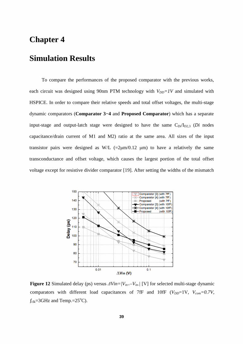
To compare the performances of the proposed comparator with the previous works,
each circuit was designed using 90nm PTM technology with VDD=1V and simulated with
HSPICE. In order to compare their relative speeds and total offset voltages, the multi-stage
dynamic comparators (Comparator 3−4 and Proposed Comparator) which has a separate
input-stage and output-latch stage were designed to have the same CDi/ID2,3 (Di nodes
capacitance/drain current of M1 and M2) ratio at the same area. All sizes of the input
transistor pairs were designed as W/L (=2µm/0.12 µm) to have a relatively the same
transconductance and offset voltage, which causes the largest portion of the total offset
voltage except for resistive divider comparator [19]. After setting the widths of the mismatch
Figure 12 Simulated delay (ps) versus ∆Vin=|Vin+–Vin-| [V] for selected multi-stage dynamic
comparators with different load capacitances of 7fF and 10fF (VDD=1V, Vcom=0.7V,
fclk=3GHz and Temp.=25oC).

40
critical transistors to have relatively large size (>1µm), the rest sizes of transistors are
optimized for high speed, low offset and less power consumption.
Figure 11 shows the simulated delay (ps) versus the input voltage difference (V) with
the different load capacitance of 7fF and 10fF for the selected multi-stage dynamic latched
comparators. Their absolute delays were measured between the 30% of the rising Clk edge to
70% of the rising output edge for the comparator from [3] and [4] and to 30% of the falling
output edge for the proposed comparator. Even with the additional inverter delays formed
from transistor M16-19, the proposed comparator outputs faster decision over the comparator
from [3] when ∆Vin is less than around 25mV with 7fF capacitance load and less than around
50mV with 10fF capacitance load since the delay of the proposed comparator is less sensitive
to the reduction of ∆Vin which is around 17ps/decade. As the size of the load gets larger, the
proposed comparator shows better overall speed over the comparator [3] since the proposed
comparator can drive more current to the load than the comparator [3] and [4] at the same
area of the output-stage.
To compare the offset voltages of each comparator, random mismatch in threshold
voltage Vth and current factor β (=µCoxW/L) were modeled as follows from (29) and (30). Avth
and Aβ are process dependent parameters and assumed to be 3mV·µm and 1%·µm
respectively in our mismatch analysis. The overall performance comparison of each
comparator is summarized in Table 2. The fifth column in Table 2 shows the resulting input-
referred total offset voltage (VOS) from 500 iterations of Monte Carlo transient simulations
with 7fF capacitance load, Vcom=0.7V and VDD=1V. The simulated result shows that the
resulting VOS of the proposed one is 16.3mV which is 3.8mV less than that of the comparator
[3] while which is 0.5 mV bigger than that of the comparator [4]; however, as shown in
Figure 11 since the proposed comparator shows much faster operation than comparator [4],
by simply reducing the size of the input tail transistor M1, the proposed comparator can get

41
an even less offset voltage than comparator [4] at faster operation. The second and third
columns show the number of transistors and total channel widths of the transistors, which can
be considered as approximate measures of circuit complexity and chip area. The fourth
column is the delays (ps) per the input voltage differences (log(∆Vin) or decade) of each
comparator. The sixth and last column in Table 2 shows that the proposed comparator
consumes even less energy than the comparator [3] while presenting more stable
delay/log(∆Vin), which means that the highest gain is delivered to the output latch stage. From
the simulation results, the dynamic voltage gain up to around 12 V/V can be easily obtained,
where around 1.7 times of the gain is produced by the inverter pairs (M18/M16 and
M19/M17) followed by Di node gain of around 7 V/V. That means that the input referred
offset voltage caused from the output latching stage mismatch is reduced by 12 (1.7 X 7)
times. Therefore, for the proposed dynamic comparator design, since the output-latch stage is
relatively offset insensitive and is able to drive larger current than other multi-stage dynamic
comparators at the same area, it does not need to be designed too big. Instead, both inverter
pairs inserted between input- and output-stage need to be designed big to lower the overall
offset voltage since they are the second dominant component of the total offset voltage.
Number of
Transistors ∑ Width [µm] |Delay [ps]/log(∆V in)| Offset Voltage [mV] Energy [fJ]/Decision
Comparator 1 [19] 10 18.4 ~ 59 ps/decade 52 mV 40.2 fJ
Comparator 2 [1] 11 18.4 ~ 61 ps/decade 20 mV 39.8 fJ
Comparator 3 [3] 14 18.4 ~ 33 ps/decade 20.1 mV 57.4 fJ
Comparator 4 [26] 15 18.4 ~ 32 ps/decade 19.1 mV 46.7 fJ
Comparator 5 [4] 15 18.3 ~ 45 ps/decade 15.8 mV 51.8 fJ
Proposed
Comparator 19 18.3 ~17 ps/decade 16.3 mV 52.8 fJ
Table 2 Performance Comparison

42
Chapter 5
Conclusion and Future Work
5.1 Conclusion
A new dynamic latched comparator which shows lower offset voltage and higher load
drivability than the conventional dynamic latched comparators has been designed. With two
additional inverters inserted between the input- and output-stage of the conventional double-
tail dynamic comparator, the gain preceding the regenerative latch stage was improved and
the complementary version of the output-latch stage, which has bigger output drive current
capability at the same area, was implemented. As a result, the circuit shows up to 19% less
offset voltage and 62% less sensitivity of the delay versus the input voltage difference
(delay/log(∆Vin)), which is about 17ps/decade, than the conventional double-tail latched
comparators at approximately the same area and power consumption.
5.2 Future Work
As mentioned earlier, since the proposed fully dynamic latched comparator can be
optimized for either the minimum offset voltage or the maximum load drivability at a limited area
according to the design specification, searching for the most suitable application can be one
topic for the future works. In addition, offset cancellation techniques can be considered for
further reduction of the offset voltage.

43
REFERENCES
1. T. Kobayashi, K. Nogami, T. Shirotori and Y. Fujimoto, “A current-controlled latch sense amplifier and a static power-saving input buffer for low-power architecture,” IEEE J. Solid-State Circuits, vol. 28, pp. 523-52, April 1993.
2. B. Wicht, T. Nirschl, and D. Schmitt-Landsiedel, “Yield and speed optimization of a latch-type voltage sense amplifier,” IEEE J. Solid-State Circuits, vol. 39, pp. 1148-1158, July 2004.
3. D. Schinkel, E. Mensink, E. Kiumperink, E. van Tuijl and B. Nauta, “A Double-Tail Latch-Type Voltage Sense Amplifier with 18ps Setup+Hold Time,” ISSCC Dig. Tech. Papers, pp. 314-315 and 605, Feb. 2007.
4. M. Miyahara, Y. Asada, P. Daehwa and A. Matsuzawa, “A Low-Noise Self-Calibrating Dynamic Comparator for High-Speed ADCs,” in Proc. A-SSCC, pp. 269-272, Nov. 2008.
5. Jun He, Sanyi Zhan, Degang Chen, and R.L. Geiger, “Analyses of Static and Dynamic Random Offset Voltages in Dynamic Comparators,” IEEE Trans. Circuits Syst. I: Reg. Papers, vol. 56, pp. 911-919, May 2009.
6. Nikoozadeh and B. Murmann, “An Analysis of Latch Comparator Offset Due to Load Capacitor Mismatch,” IEEE Trans. Circuits Syst. II: Exp. Briefs, vol. 53, no. 12, pp. 1398-1402, Dec. 2006
7. B. Murmann et al., "Impact of scaling on analog performance and associated modeling needs," IEEE Trans. Electron Devices, vol. 53, no. 9, pp. 2160-2167, Sep. 2006.
8. Philip E. Allen and Douglas R. Holberg, CMOS Analog Circuit Design, 2nd ed. New York, NY: Oxford, 2002.
9. B. Razavi, Principles of Data Conversion System Design. Piscataway, NJ: IEEE Press, 1995
10. “Comparators," MT-083 Tutorial, Analog Devices Inc, 2009, [Online]. Available: http://www.analog.com/static/imported-files/tutorials/MT-083.pdf [Accessed: April 23, 2010]
11. Pedro M.Figueiredo, Joao C.Vital, “Kickback Noise Reduction Techniques for CMOS Latched Comparator”, IEEE Transactions on Circuits and Systems, vol.53, no.7, pp.541-545, July 2006.

44
12. H. Fiedler, B. Hoefflinger, W. Demmer, and P. Draheim, “A 5-bit building block for 20 MHz A/D converters,” IEEE J. Solid-State Circuits, vol. SC-16, no. 3, pp. 151–155, Jun. 1981.
13. J. Robert, G. Temes, V. Valencic, R. Dessoulavy, and P. Deval, “A 16-bit low-voltage CMOS A/D converter,” IEEE J. Solid-State Circuits, vol. SC-22, no. 2, pp. 157–163, Apr. 1987.
14. B. Song, S. Lee, and M. Tompsett, “A 10-b 15-MHz CMOS recycling two-step A/D converter,” IEEE J. Solid-State Circuits, vol. 25, no. 6, pp. 1328–1338, Dec. 1990.
15. S. Lewis, H. Fetterman, G. Gross, R. Ramachandran, and T. Viswanathan, “A 10-b 20-Msample/s analog-to-digital converter,” IEEE J. Solid-State Circuits, vol. 27, no. 3, pp. 351–358, Mar. 1992.
16. B. Nauta and A. Venes, “A 70-MS/s 110-mW 8-b CMOS folding and interpolating A/D converter,” IEEE J. Solid-State Circuits, vol. 30, no. 12, pp. 1302–1308, Dec. 1995.
17. A. Venes and R. Plassche, “An 80-MHz, 80-mW, 8-b CMOS folding A/D converter with distributed track-and-hold preprocessing,” IEEE J. Solid-State Circuits, vol. 31, no. 12, pp. 1846–1853, Dec. 1996.
18. A. Yukawa, “A CMOS 8-bit high-speed A/D converter IC,” IEEE J. Solid-State Circuits, vol. SC-20, no. 3, pp. 775–779, Jun. 1985.
19. S. Sutarja and P. Gray, “A pipelined 13-bit, 250-ks/s, 5-V analog-to-digital converter,” IEEE J. Solid-State Circuits, vol. 23, no. 6, pp. 1316–1323, Dec. 1988.
20. G. Yin, F. Eynde, and W. Sansen, “A high-speed CMOS comparator with 8-b resolution,” IEEE J. Solid-State Circuits, vol. 27, no. 2, pp. 208–211, Feb. 1992.
21. P. Amaral, J. Goes, N. Paulino, and A. Steiger-Garção, “An improved low-voltage low-power CMOS comparator to be used in high-speed pipeline ADCs,” in Proc. IEEE Int. Symp. Circuits Syst., May 2002, vol. 5, pp. 141–144.
22. K. Uyttenhove and M. Steyaert, “A 1.8 V 6-bit 1.3-GHz flash ADC in 0.25 _m CMOS,” IEEE J. Solid-State Circuits, vol. 38, no. 7, pp. 1115–1122, Jul. 2003.
23. T. Cho and P. Gray, “A 10 b, 20 Msample/s, 35 mW pipeline A/D converter,” IEEE J. Solid-State Circuits, vol. 30, no. 3, pp. 166–172, Mar. 1995.
24. L. Sumanen, M. Waltari, K. Halonen, “A Mismatch Insensitive CMOS Dynamic Comparator for Pipeline A/D Converters,” IEEE ICECS, vol. 1, pp. 32 - 35, Dec. 2000.
25. Sumanen, M. Waltari, V. Hakkarainen, K. Halonen, “CMOS Dynamic Comparators for Pipeline A/D Converters,” IEEE ISCAS, vol. 5, pp. 157 - 160, May 2002.

45
26. M. van Elzakker, A.J.M. van Tuijl, P.F.J. Geraedts, D. Schinkel, E.A.M. Klumperink and B. Nauta, "A 1.9µW 4.4fJ/Conversion-step 10b 1MS/s Charge-Redistribution ADC," ISSCC Dig. Tech. Papers, pp. 244–245, February 2008.
27. M. J. M. Pelgrom, A. C. J. Duinmaijer, and A. P. G. Weblbers, “Matching properties of MOS transistors,” IEEE J. Solid-State Circuits, vol. 24, no. 10, pp. 1433–1439, Oct. 1995.
28. B. Razavi and B. A. Wooley, “Design techniques for high-speed highresolution comparators,” IEEE J. Solid-State Circuits, vol. 27, no. 6, pp. 1916–1926, Dec. 1992.
29. K. L. J. Wong et al., “Offset Compensation in Comparators with Minimum Input-Referred Supply Noise,” IEEE Journal of Solid-State Circuits, vol. 39, No. 5, pp. 837-840, May 2004.
30. “The Design of a Two-Stage Comaprator,” [Online]. Available: http://people.rit.edu/ssm8867/pdf/analogbody.pdf [Accessed: April 23, 2010]
31. S. Kale and R. S. Gamad, “Design of a CMOS Comparator for Low Power and High Speed,” Internationl Journal of Electronic Engineering Research, vol. 2, no. 1, pp. 29-34, 2010
32. P. Nuzzo, F. De Bernardinis, P. Terreni, and G. Van der Plas, “Noise analysisof regenerative comparators for reconfigurable ADC architectures,” IEEE Trans. Circuits Syst. I, vol. 55, no. 6, pp. 1441–1454, July 2008.
33. T. Sepke, P. Holloway, C. G. Sodini and H. S. Lee, “Noise Analysis for Comparator-Based Circuits,” IEEE Trans. Circuits Syst. I: Reg. Papers, vol. 56, no. 3, pp. 541–553, March 2009.
34. Art Zirger, “Random Offset in CMOS IC Design,” [Online]. Available: http://ecee.colorado.edu/~ecen4827/lectures/Random_Offset_CMOS_IC_Design_CU_Lecture_Art_Zirger.pdf [Accessed: April 23, 2010]
35. H. Khorramabadi, “EE247 Analog-Digital Interface Integrated Circuits,” [Online]. Available: http://inst.eecs.berkeley.edu/~ee247/fa09/files07/lectures/L19_2_f09.pdf [Accessed: April 23, 2010]
36. H.J. Jeon, Y.B. Kim, “A Low-offset High-speed Double-tail Dual-rail Dynamic Latched Comparator,” ACM GLSVLSI’10(Great Lakes Symposium on VLSI), May 16-18, 2010
37. 90nm Predictive Technology Model (PTM), [Online] Available: http://www.eas.asu.edu/~ptm/latest.htm [Accessed: April 23, 2010]

46
Appendix A
90nm PTM Model File:
*************************************************** *************************************** * Customized PTM 90nm NMOS *************************************************** *************************************** .model nmos nmos level = 54 +version = 4.0 binunit = 1 paramchk = 1 mobmod = 0 +capmod = 2 igcmod = 1 igbmod = 1 geomod = 1 +diomod = 1 rdsmod = 0 rbodymod = 1 rgatemod = 1 +permod = 1 acnqsmod = 0 trnqsmod = 0 * parameters related to the technology node +tnom = 27 epsrox = 3.9 +eta0 = 0.0074 nfactor = 1.7 wint = 5e-09 +cgso = 1.9e-10 cgdo = 1.9e-10 xl = -4e-08 * parameters customized by the user +toxe = 2.05e-09 toxp = 1.4e-09 toxm = 2.05e-09 toxref = 2.05e-09 +dtox = 6.5e-10 lint = 7.5e-09 +vth0 = 0.408 k1 = 0.486 u0 = 0.05383 vsat = 113760 +rdsw = 180 ndep = 2.02e+18 xj = 2.8e-08 * secondary parameters +ll = 0 wl = 0 lln = 1 wln = 1 +lw = 0 ww = 0 lwn = 1 wwn = 1 +lwl = 0 wwl = 0 xpart = 0 +k2 = 0.01 k3 = 0 +k3b = 0 w0 = 2.5e-006 dvt0 = 1 dvt1 = 2 +dvt2 = -0.032 dvt0w = 0 dvt1w = 0 dvt2w = 0 +dsub = 0.1 minv = 0.05 voffl = 0 dvtp0 = 1.0e-009 +dvtp1 = 0.1 lpe0 = 0 lpeb = 0 +ngate = 2e+020 nsd = 2e+020 phin = 0 +cdsc = 0.000 cdscb = 0 cdscd = 0 cit = 0 +voff = -0.13 etab = 0 +vfb = -0.55 ua = 6e-010 ub = 1.2e-018 +uc = 0 a0 = 1.0 ags = 1e-020 +a1 = 0 a2 = 1.0 b0 = 0 b1 = 0 +keta = 0.04 dwg = 0 dwb = 0 pclm = 0.04 +pdiblc1 = 0.001 pdiblc2 = 0.001 pdiblcb = -0.005 drout = 0.5 +pvag = 1e-020 delta = 0.01 pscbe1 = 8.14e+008 pscbe2 = 1e-007 +fprout = 0.2 pdits = 0.08 pditsd = 0.23 pditsl = 2.3e+006 +rsh = 5 rsw = 85 rdw = 85 +rdswmin= 0 rdwmin = 0 rswmin = 0 prwg = 0 +prwb = 6.8e-011 wr = 1 alpha0 = 0.074 alpha1 = 0.005 +beta0 = 30 agidl = 0.0002 bgidl = 2.1e+009 cgidl = 0.0002 +egidl = 0.8 +aigbacc = 0.012 bigbacc = 0.0028 cigbacc = 0.002 +nigbacc = 1 aigbinv = 0.014 bigbinv = 0.004 cigbinv = 0.004 +eigbinv = 1.1 nigbinv = 3 aigc = 0.012 bigc = 0.0028 +cigc = 0.002 aigsd = 0.012 bigsd = 0.0028 cigsd = 0.002

47
+nigc = 1 poxedge =1 pigcd = 1 ntox = 1 +xrcrg1 = 12 xrcrg2 = 5 +cgbo = 2.56e-011 cgdl = 2.653e-10 +cgsl = 2.653e-10 ckappas = 0.03 ckappad = 0.03 acde = 1 +moin = 15 noff = 0.9 voffcv = 0.02 +kt1 = -0.11 kt1l = 0 kt2 = 0.022 ute = -1.5 +ua1 = 4.31e-009 ub1 = 7.61e-018 uc1 = -5.6e-011 prt = 0 +at = 33000 +fnoimod = 1 tnoimod = 0 +jss = 0.0001 jsws = 1e-011 jswgs = 1e-010 njs = 1 +ijthsfwd= 0.01 ijthsrev = 0.001 bvs = 10 xjbvs = 1 +jsd = 0.0001 jswd = 1e-011 jswgd = 1e-010 njd = 1 +ijthdfwd= 0.01 ijthdrev = 0.001 bvd = 10 xjbvd = 1 +pbs = 1 cjs = 0.0005 mjs = 0.5 pbsws = 1 +cjsws = 5e-010 mjsws = 0.33 pbswgs = 1 cjswgs = 3e-010 +mjswgs = 0.33 pbd = 1 cjd = 0.0005 mjd = 0.5 +pbswd = 1 cjswd = 5e-010 mjswd = 0.33 pbswgd = 1 +cjswgd = 5e-010 mjswgd = 0.33 tpb = 0.005 tcj = 0.001 +tpbsw = 0.005 tcjsw = 0.001 tpbswg = 0.005 tcjswg = 0.001 +xtis = 3 xtid = 3 +dmcg = 0e-006 dmci = 0e-006 dmdg = 0e-006 dmcgt = 0e-007 +dwj = 0.0e-008 xgw = 0e-007 xgl = 0e-008 +rshg = 0.4 gbmin = 1e-010 rbpb = 5 rbpd = 15 +rbps = 15 rbdb = 15 rbsb = 15 ngcon = 1 *************************************************** *************************************** * Customized PTM 90nm PMOS *************************************************** *************************************** .model pmos pmos level = 54 +version = 4.0 binunit = 1 paramchk = 1 mobmod = 0 +capmod = 2 igcmod = 1 igbmod = 1 geomod = 1 +diomod = 1 rdsmod = 0 rbodymod = 1 rgatemod = 1 +permod = 1 acnqsmod = 0 trnqsmod = 0 * parameters related to the technology node +tnom = 27 epsrox = 3.9 +eta0 = 0.0074 nfactor = 1.7 wint = 5e-09 +cgso = 1.9e-10 cgdo = 1.9e-10 xl = -4e-08 * parameters customized by the user +toxe = 2.15e-09 toxp = 1.4e-09 toxm = 2.15e-09 toxref = 2.15e-09 +dtox = 7.5e-10 lint = 7.5e-09 +vth0 = -0.354 k1 = 0.422 u0 = 0.00678 vsat = 70000 +rdsw = 200 ndep = 1.52e+18 xj = 2.8e-08 * secondary parameters +ll = 0 wl = 0 lln = 1 wln = 1 +lw = 0 ww = 0 lwn = 1 wwn = 1 +lwl = 0 wwl = 0 xpart = 0 +k2 = -0.01 k3 = 0

48
+k3b = 0 w0 = 2.5e-006 dvt0 = 1 dvt1 = 2 +dvt2 = -0.032 dvt0w = 0 dvt1w = 0 dvt2w = 0 +dsub = 0.1 minv = 0.05 voffl = 0 dvtp0 = 1.0e-009 +dvtp1 = 0.05 lpe0 = 0 lpeb = 0 +ngate = 2e+020 nsd = 2e+020 phin = 0 +cdsc = 0.000 cdscb = 0 cdscd = 0 cit = 0 +voff = -0.126 etab = 0 +vfb = 0.55 ua = 2.0e-010 ub = 0.5e-018 +uc = 0 a0 = 1.0 ags = 1e-020 +a1 = 0 a2 = 1.0 b0 = -1e-020 b1 = 0 +keta = -0.047 dwg = 0 dwb = 0 pclm = 0.12 +pdiblc1 = 0.001 pdiblc2 = 0.001 pdiblcb =3.4e-08 drout = 0.56 +pvag = 1e-020 delta = 0.01 pscbe1 = 8.14e+008 pscbe2 = 9.58e-007 +fprout = 0.2 pdits = 0.08 pditsd = 0.23 pditsl = 2.3e+006 +rsh = 5 rsw = 85 rdw = 85 +rdswmin= 0 rdwmin = 0 rswmin = 0 prwg = 3.22e-008 +prwb = 6.8e-011 wr = 1 alpha0 = 0.074 alpha1 = 0.005 +beta0 = 30 agidl = 0.0002 bgidl = 2.1e+009 cgidl = 0.0002 +egidl = 0.8 +aigbacc = 0.012 bigbacc = 0.0028 cigbacc = 0.002 +nigbacc = 1 aigbinv = 0.014 bigbinv = 0.004 cigbinv = 0.004 +eigbinv = 1.1 nigbinv = 3 aigc = 0.69 bigc = 0.0012 +cigc = 0.0008 aigsd = 0.087 bigsd = 0.0012 cigsd = 0.0008 +nigc = 1 poxedge = 1 pigcd = 1 ntox = 1 +xrcrg1 = 12 xrcrg2 = 5 +cgbo = 2.56e-011 cgdl = 2.653e-10 +cgsl = 2.653e-10 ckappas = 0.03 ckappad = 0.03 acde = 1 +moin = 15 noff = 0.9 voffcv = 0.02 +kt1 = -0.11 kt1l = 0 kt2 = 0.022 ute = -1.5 +ua1 = 4.31e-009 ub1 = 7.61e-018 uc1 = -5.6e-011 prt = 0 +at = 33000 +fnoimod = 1 tnoimod = 0 +jss = 0.0001 jsws = 1e-011 jswgs = 1e-010 njs = 1 +ijthsfwd= 0.01 ijthsrev = 0.001 bvs = 10 xjbvs = 1 +jsd = 0.0001 jswd = 1e-011 jswgd = 1e-010 njd = 1 +ijthdfwd= 0.01 ijthdrev = 0.001 bvd = 10 xjbvd = 1 +pbs = 1 cjs = 0.0005 mjs = 0.5 pbsws = 1 +cjsws = 5e-010 mjsws = 0.33 pbswgs = 1 cjswgs = 3e-010 +mjswgs = 0.33 pbd = 1 cjd = 0.0005 mjd = 0.5 +pbswd = 1 cjswd = 5e-010 mjswd = 0.33 pbswgd = 1 +cjswgd = 5e-010 mjswgd = 0.33 tpb = 0.005 tcj = 0.001 +tpbsw = 0.005 tcjsw = 0.001 tpbswg = 0.005 tcjswg = 0.001 +xtis = 3 xtid = 3 +dmcg = 0e-006 dmci = 0e-006 dmdg = 0e-006 dmcgt = 0e-007 +dwj = 0.0e-008 xgw = 0e-007 xgl = 0e-008 +rshg = 0.4 gbmin = 1e-010 rbpb = 5 rbpd = 15 +rbps = 15 rbdb = 15 rbsb = 15 ngcon = 1

49
Appendix B
HSPICE Netlist Files for Simulated Comparator Circuits:
1. Comparator 1 [19]
*************************************************** *************************************** .title 'Optimized Lewis-Gray Dynamic Latched Comparator' .include "..\models\90ntt.sp" .include "..\models\90ptt.sp" *** key parameters ******************************** ****************************************** .param v_supply=1 .param vdiff=20m .param vcom=0.7 .param clk_freq=3G *** Netlist *************************************** ***************************************** v00 gnda 0 0 v0 vdda gnda v_supply v1 vcm gnda vcom v2 vdd gnd v_supply *** Clk ******************************************* **************************************** v_clk clk gnda PULSE ( v3 v4 td tr tf pw per ) .param v3=0 v4=1 + td=50p td2=50p + tr='trf_ratio*per' tf='trf_ratio*per' + pw='per/2-(tr+tf)/2' + per='1/clk_freq' + trf_ratio=0.01 *** Clk buffers *********************************** ****************************************** *mpb11 b_clk vclk vdd vdd pmos L='lmin' W='0.25*(wn1)*3*4' *mnb11 b_clk vclk 0 0 nmos L='lmin' W='0.25*(wn1)*3' *mpb12 clk b_clk vdd vdd pmos L='lmin' W='0.25*(wn1)*3*4' *mnb12 clk b_clk 0 0 nmos L='lmin' W='0.25*(wn1)*3' *** Diff Input ************************************ ****************************************** vin+ in+ vcm PULSE ( '-vdiff' 'vdiff' td_in 0.01n 0.01n 0.32n 0.66n ) vref in- vcm PULSE ( 0 0 td_in 0.01n 0.01n 0.32n 0.66n ) .param td_in=0.3n ************ input stage ************************** ****************************************** m1a Di- in+ 0 0 nmos L='lmin2' W='wn1' m1b Di+ in- 0 0 nmos L='lmin2' W='wn1' *m2a Di- vref- 0 0 nmos L='lmin2' W='wn2' *m2b Di+ vref+ 0 0 nmos L='lmin2' W='wn2' m3 1 out+ Di+ 0 nmos L='lmin3' W='wn3' m4 2 out- Di- 0 nmos L='lmin3' W='wn3' m5 out- clk 1 0 nmos L='lmin' W='wn5'

50
m6 out+ clk 2 0 nmos L='lmin' W='wn5' m7 out- out+ vdd vdd pmos L='lmin' W='wp7' m8 out+ out- vdd vdd pmos L='lmin' W='wp7' m9 out- clk vdd vdd pmos L='lmin' W='wp9' m10 out+ clk vdd vdd pmos L='lmin' W='wp9' .param lmin=100n + lmin2=120n + lmin3=120n + wn1=1u + wn3=3u + wn5=1.8u + wp7=1.4u + wp9=1.8u c1 out+ gnd cload c2 out- gnd cload .param cload=7f ** Analysis setup ********************************* ****************************************** .TEMP 25 .OPTIONS POST .WIDTH OUT=80 .tran 1p 1n sweep 5m 50m 5m .print di=par('abs(v(di-)-v(di+))') .print vout_pmn=par('abs(v(out+)-v(out-))') .measure delay1 + trig v(clk) val='v_supply*0.3' rise=2 + targ v(out-) val='v_supply*0.3' fall=1 .measure delay2 + trig v(clk) val='v_supply*0.3' rise=3 + targ v(out+) val='v_supply*0.3' fall=2 .measure Delay_ave param='(delay1+delay2)/2' .meas tran qtot integral i(v2) from=373p to=706p .meas tran iave avg i(v2) from=373p to=706p .meas etot param='v_supply*qtot' .meas ptot param='v_supply*iave' .END *************************************************** ***************************************

51
2. Comparator 2 [1]
*************************************************** ***************************************
.title 'Optimized Latch-type Voltage SA' .include "..\models\90ntt.sp" .include "..\models\90ptt.sp" *** key parameters ******************************** ****************************************** .param v_supply=1 .param vdiff=20m .param vcom=0.7 .param clk_freq=3G *** Netlist *************************************** ***************************************** v00 gnda 0 0 v0 vdda gnda v_supply v1 vcm gnda vcom v2 vdd gnd v_supply *** Clk ******************************************* **************************************** v_clk clk gnda PULSE ( v3 v4 td tr tf pw per ) .param v3=0 v4=1 + td=50p td2=50p + tr='trf_ratio*per' tf='trf_ratio*per' + pw='per/2-(tr+tf)/2' + per='1/clk_freq' + trf_ratio=0.01 *** Clk buffers *********************************** ******************************************
*mpb11 b_clk vclk vdd vdd pmos L='lmin' W='0.25*(wn1)*3*4' *mnb11 b_clk vclk 0 0 nmos L='lmin' W='0.25*(wn1)*3' *mpb12 clk b_clk vdd vdd pmos L='lmin' W='0.25*(wn1)*3*4' *mnb12 clk b_clk 0 0 nmos L='lmin' W='0.25*(wn1)*3' *** Diff Input ************************************ ******************************************
vin+ in+ vcm PULSE ( '-vdiff' 'vdiff' td_in 0.01n 0.01n 0.32n 0.66n ) vref in- vcm PULSE ( 0 0 td_in 0.01n 0.01n 0.32n 0.66n ) .param td_in=0.3n ************ input stage ************************** ****************************************** mn1 1 clk gnd gnd nmos L='lmin1' W='wn1' mn2 Di- in+ 1 gnd nmos L='lmin2' W='wn2' mn3 Di+ in- 1 gnd nmos L='lmin2' W='wn2' mp4 out- clk vdd vdd pmos L='lmin' W='wp4' mp5 out+ clk vdd vdd pmos L='lmin' W='wp4' mn6 out- out+ Di- gnd nmos L='lmin' W='wn6' mn7 out+ out- Di+ gnd nmos L='lmin' W='wn6' mp8 out- out+ vdd vdd pmos L='lmin' W='wp8' mp9 out+ out- vdd vdd pmos L='lmin' W='wp8' mp10 Di- clk vdd vdd pmos L='lmin' W='wp10' mp11 Di+ clk vdd vdd pmos L='lmin' W='wp10'

52
.param lmin=100n + lmin1=120n + lmin2=120n + wn1=2u + wn2=2u + wp4=2u + wn6=3u + wp8=0.8u + wp10=0.4u c1 out+ gnd cload c2 out- gnd cload .param cload=7f ** Analysis setup ********************************* ****************************************** .TEMP 25 .OPTIONS POST .WIDTH OUT=80 .tran 1p 1n sweep 5m 50m 5m .print di=par('abs(v(di-)-v(di+))') .print vout_pmn=par('abs(v(out+)-v(out-))') .measure delay1 + trig v(clk) val='v_supply*0.3' rise=2 + targ v(out-) val='v_supply*0.3' fall=1 .measure delay2 + trig v(clk) val='v_supply*0.3' rise=3 + targ v(out+) val='v_supply*0.3' fall=2 .measure Delay_ave param='(delay1+delay2)/2' .meas tran qtot integral i(v2) from=373p to=706p .meas tran iave avg i(v2) from=373p to=706p .meas etot param='v_supply*qtot' .meas ptot param='v_supply*iave' .END *************************************************** ***************************************

53
3. Comparator 3 [3]
.title 'Double-Tail SA' .include "..\models\90ntt.sp" .include "..\models\90ptt.sp" *** key parameters ******************************** ****************************************** .param v_supply=1 .param vdiff=20m .param vcom=0.7 .param clk_freq=3G *** Netlist *************************************** ***************************************** v00 gnda 0 0 v0 vdda gnda v_supply v1 vcm gnda vcom v2 vdd gnd v_supply *** Clk ******************************************* **************************************** v_clk clk gnda PULSE ( v3 v4 td tr tf pw per ) *v_clkb vclkb gnda PULSE ( v4 v3 td2 tr tf pw per ) mpb13 clkb clk vdd vdd pmos L='lmin' W='wp14' mnb13 clkb clk 0 0 nmos L='lmin' W='wn13' .param wp14=0.6u + wn13=0.6u .param v3=0 v4=1 + td=50p td2=50p + tr='trf_ratio*per' tf='trf_ratio*per' + pw='per/2-(tr+tf)/2' + per='1/clk_freq' + trf_ratio=0.01 *** Clk buffers *********************************** ****************************************** *mpb11 b_clk vclk vdd vdd pmos L='lmin' W='0.25*(wn1)*3*4' *mnb11 b_clk vclk 0 0 nmos L='lmin' W='0.25*(wn1)*3' *mpb12 clk b_clk vdd vdd pmos L='lmin' W='0.25*(wn1)*3*4*4' *mnb12 clk b_clk 0 0 nmos L='lmin' W='0.25*(wn1)*3*4' *mpb111 b_clkb vclkb vdd vdd pmos L='lmin' W='0.25*(wn1)*3*4' *mnb111 b_clkb vclkb 0 0 nmos L='lmin' W='0.25*(wn1)*3' *mpb121 clkb b_clkb vdd vdd pmos L='lmin' W='0.25*(wn1)*3*4*4' *mnb121 clkb b_clkb 0 0 nmos L='lmin' W='0.25*(wn1)*3*4' *** Diff Input ************************************ ****************************************** vin+ in+ vcm PULSE ( '-vdiff' 'vdiff' td_in 0.01n 0.01n 0.32n 0.66n ) vref in- vcm PULSE ( 0 0 td_in 0.01n 0.01n 0.32n 0.66n ) .param td_in=0.3n ************ input stage ************************** ****************************************** mn1 1 clk gnd gnd nmos L='lmin1' W='wn1' mn2 Di- in+ 1 gnd nmos L='lmin2' W='wn2' mn3 Di+ in- 1 gnd nmos L='lmin2' W='wn2' mp4 Di- clk vdd vdd pmos L='lmin' W='wp4' mp5 Di+ clk vdd vdd pmos L='lmin' W='wp4'

54
.param lmin=100n + lmin1=120n + lmin2=120n + wn1=0.44u + wn2=2u + wp4=0.5u *** output stage ********************************** ****************************************** mn6 out+ out- gnd gnd nmos L='lmin' W='wn6' mn7 out- out+ gnd gnd nmos L='lmin' W='wn6' mp8 out+ out- 2 vdd pmos L='lmin' W='wp8' mp9 out- out+ 2 vdd pmos L='lmin' W='wp8' mn10 out+ Di- gnd gnd nmos L='lmin' W='wn10' mn11 out- Di+ gnd gnd nmos L='lmin' W='wn10' mp12 2 clkb vdd vdd pmos L='lmin' W='wp12' .param wp12=4u + wn6=0.5u + wp8=1.8u + wn10=1.6u c1 out+ gnd cload c2 out- gnd cload .param cload=7f ** Analysis setup ********************************* ****************************************** .TEMP 25 .OPTIONS POST .WIDTH OUT=80 .tran 1p 1n sweep 5m 50m 5m .print di=par('abs(v(di-)-v(di+))') .print vout_pmn=par('abs(v(out+)-v(out-))') .measure delay1 + trig v(clk) val='v_supply*0.3' rise=2 + targ v(out+) val='v_supply*0.7' rise=1 .measure delay2 + trig v(clk) val='v_supply*0.3' rise=3 + targ v(out-) val='v_supply*0.7' rise=2 .measure Delay_ave param='(delay1+delay2)/2' .meas tran qtot integral i(v2) from=373p to=706p .meas tran iave avg i(v2) from=373p to=706p .meas etot param='v_supply*qtot' .meas ptot param='v_supply*iave' .END *************************************************** ***************************************

55
4. Comparator 4 [26]
.title 'NEW Two-stage(DT) Dynamic Latched Comparator' .include "..\models\90ntt.sp" .include "..\models\90ptt.sp" *** key parameters ******************************** ****************************************** .param v_supply=1 .param vdiff=20m .param vcom=0.7 .param clk_freq=3G *** Netlist *************************************** ***************************************** v00 gnda 0 0 v0 vdda gnda v_supply v1 vcm gnda vcom v2 vdd gnd v_supply *** Clk ******************************************* **************************************** v_clk clk gnda PULSE ( v3 v4 td tr tf pw per ) *v_clkb vclkb gnda PULSE ( v4 v3 td2 tr tf pw per ) mpb15 clkb clk vdd vdd pmos L='lmin' W='wp15' mnb14 clkb clk 0 0 nmos L='lmin' W='wn14' .param wp15=0.2u + wn14=0.2u .param v3=0 v4=1 + td=50p td2=50p + tr='trf_ratio*per' tf='trf_ratio*per' + pw='per/2-(tr+tf)/2' + per='1/clk_freq' + trf_ratio=0.01 *** Clk buffers *********************************** ****************************************** *mpb11 b_clk vclk vdd vdd pmos L='lmin' W='0.25*(wn1)*3*4' *mnb11 b_clk vclk 0 0 nmos L='lmin' W='0.25*(wn1)*3' *mpb12 clk b_clk vdd vdd pmos L='lmin' W='0.25*(wn1)*3*4*4' *mnb12 clk b_clk 0 0 nmos L='lmin' W='0.25*(wn1)*3*4' *mpb111 b_clkb vclkb vdd vdd pmos L='lmin' W='0.25*(wn1)*3*4' *mnb111 b_clkb vclkb 0 0 nmos L='lmin' W='0.25*(wn1)*3' *mpb121 clkb b_clkb vdd vdd pmos L='lmin' W='0.25*(wn1)*3*4*4' *mnb121 clkb b_clkb 0 0 nmos L='lmin' W='0.25*(wn1)*3*4' *** Diff Input ************************************ ****************************************** vin+ in+ vcm PULSE ( '-vdiff' 'vdiff' td_in 0.01n 0.01n 0.32n 0.66n ) vref in- vcm PULSE ( 0 0 td_in 0.01n 0.01n 0.32n 0.66n ) .param td_in=0.3n ************ input stage ************************** ****************************************** mn1 1 clk gnd gnd nmos L='lmin1' W='wn1' mn2 Di- in+ 1 gnd nmos L='lmin2' W='wn2' mn3 Di+ in- 1 gnd nmos L='lmin2' W='wn2' mp4 Di- clk vdd vdd pmos L='lmin' W='wp4' mp5 Di+ clk vdd vdd pmos L='lmin' W='wp4'

56
.param lmin=100n + lmin1=120n + lmin2=120n + wn1=0.4u + wn2=2u + wp4=0.6u ************ output stage ************************* ****************************************** mn6 out+ out- gnd gnd nmos L='lmin' W='wn6' mn7 out- out+ gnd gnd nmos L='lmin' W='wn6' mp8 2 out- vdd vdd pmos L='lmin' W='wp8' mp9 3 out+ vdd vdd pmos L='lmin' W='wp8' mp10 out+ Di- 2 vdd pmos L='lmin' W='wp10' mp11 out- Di+ 3 vdd pmos L='lmin' W='wp10' mn12 out+ clkb gnd gnd nmos L='lmin' W='wn12' mn13 out- clkb gnd gnd nmos L='lmin' W='wn12' .param wn6=0.8u + wp8=2u + wp10=3u + wn12=0.4u c1 out+ gnd cload c2 out- gnd cload .param cload=7f ** Analysis setup ********************************* ****************************************** .TEMP 25 .OPTIONS POST .WIDTH OUT=80 .tran 1p 1n sweep 5m 50m 5m .print di=par('abs(v(di-)-v(di+))') .print vout_pmn=par('abs(v(out+)-v(out-))') .measure delay1 + trig v(clk) val='v_supply*0.3' rise=2 + targ v(out+) val='v_supply*0.7' rise=1 .measure delay2 + trig v(clk) val='v_supply*0.3' rise=3 + targ v(out-) val='v_supply*0.7' rise=2 .measure Delay_ave param='(delay1+delay2)/2' .meas tran qtot integral i(v2) from=373p to=706p .meas tran iave avg i(v2) from=373p to=706p .meas etot param='v_supply*qtot' .meas ptot param='v_supply*iave' .END *************************************************** ***************************************

57
5. Comparator 5 [4]
.title 'Two-stage Dynamic Latched Comparator from JNP' .include "..\models\90ntt.sp" .include "..\models\90ptt.sp" *** key parameters ******************************** ****************************************** .param v_supply=1 .param vdiff=20m .param vcom=0.7 .param clk_freq=3G *** Netlist *************************************** ***************************************** v00 gnda 0 0 v0 vdda gnda v_supply v1 vcm gnda vcom v2 vdd gnd v_supply *** Clk ******************************************* **************************************** v_clk clk gnda PULSE ( v3 v4 td tr tf pw per ) *v_clkb vclkb gnda PULSE ( v4 v3 td2 tr tf pw per ) mpb15 clkb clk vdd vdd pmos L='lmin' W='wp15' mnb14 clkb clk 0 0 nmos L='lmin' W='wn14' .param wp15=0.2u + wn14=0.2u .param v3=0 v4=1 + td=50p td2=50p + tr='trf_ratio*per' tf='trf_ratio*per' + pw='per/2-(tr+tf)/2' + per='1/clk_freq' + trf_ratio=0.01 *** Clk buffers *********************************** ****************************************** *mpb11 b_clk vclk vdd vdd pmos L='lmin' W='0.25*(wn1)*3*4' *mnb11 b_clk vclk 0 0 nmos L='lmin' W='0.25*(wn1)*3' *mpb12 clk b_clk vdd vdd pmos L='lmin' W='0.25*(wn1)*3*4*4' *mnb12 clk b_clk 0 0 nmos L='lmin' W='0.25*(wn1)*3*4' *** Diff Input ************************************ ****************************************** vin+ in+ vcm PULSE ( '-vdiff' 'vdiff' td_in 0.01n 0.01n 0.32n 0.66n ) vref in- vcm PULSE ( 0 0 td_in 0.01n 0.01n 0.32n 0.66n ) .param td_in=0.3n ************ input stage ************************** ****************************************** mn1 1 clk gnd gnd nmos L='lmin1' W='wn1' mn2 Di- in+ 1 gnd nmos L='lmin2' W='wn2' mn3 Di+ in- 1 gnd nmos L='lmin2' W='wn2' mp4 Di- clk vdd vdd pmos L='lmin' W='wp4' mp5 Di+ clk vdd vdd pmos L='lmin' W='wp4'

58
.param lmin=100n + lmin1=120n + lmin2=120n + wn1=0.9u + wn2=2u + wp4=0.8u ************ output stage ************************* ****************************************** mn6 out+ out- gnd gnd nmos L='lmin' W='wn6' mn7 out- out+ gnd gnd nmos L='lmin' W='wn6' mp8 out+ out- 2 vdd pmos L='lmin' W='wp8' mp9 out- out+ 3 vdd pmos L='lmin' W='wp8' mn10 out+ Di- gnd gnd nmos L='lmin' W='wn10' mn11 out- Di+ gnd gnd nmos L='lmin' W='wn10' mp12 2 Di- vdd vdd pmos L='lmin' W='wp12' mp13 3 Di+ vdd vdd pmos L='lmin' W='wp12' mn14 2 Di- gnd gnd nmos L='lmin' W='wn14' mn15 3 Di+ gnd gnd nmos L='lmin' W='wn14' .param wn6=0.5u + wp8=1.6u + wp12=2.6u + wn10=1u + wn14=0.2u c1 out+ gnd cload c2 out- gnd cload .param cload=7f ** Analysis setup ********************************* ****************************************** .TEMP 25 .OPTIONS POST .WIDTH OUT=80 .tran 1p 1n sweep 5m 50m 5m .print di=par('abs(v(di-)-v(di+))') .print vout_pmn=par('abs(v(out+)-v(out-))') .measure delay1 + trig v(clk) val='v_supply*0.3' rise=2 + targ v(out+) val='v_supply*0.7' rise=1 .measure delay2 + trig v(clk) val='v_supply*0.3' rise=3 + targ v(out-) val='v_supply*0.7' rise=2 .measure Delay_ave param='(delay1+delay2)/2' .meas tran qtot integral i(v2) from=373p to=706p .meas tran iave avg i(v2) from=373p to=706p .meas etot param='v_supply*qtot' .meas ptot param='v_supply*iave' .END *************************************************** ***************************************
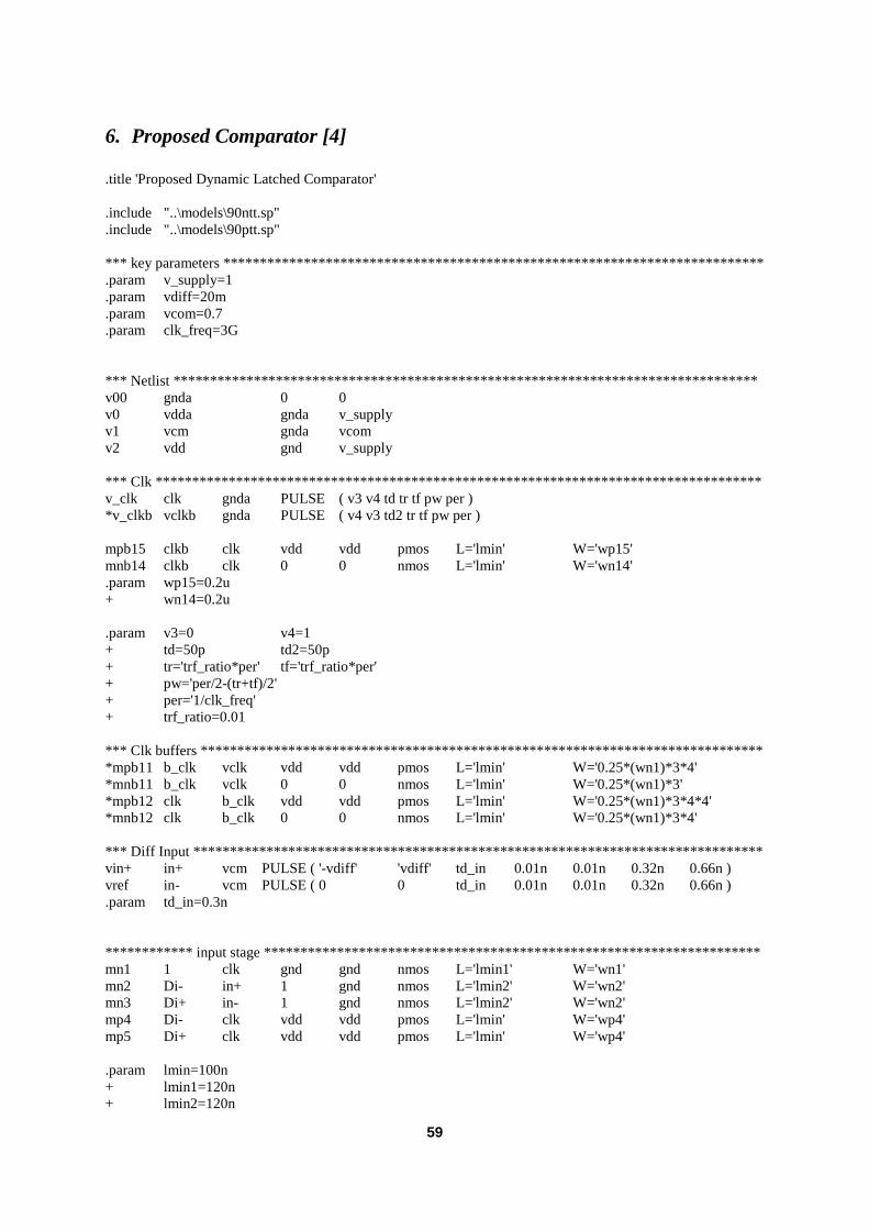
59
6. Proposed Comparator [4]
.title 'Proposed Dynamic Latched Comparator' .include "..\models\90ntt.sp" .include "..\models\90ptt.sp" *** key parameters ******************************** ****************************************** .param v_supply=1 .param vdiff=20m .param vcom=0.7 .param clk_freq=3G *** Netlist *************************************** ***************************************** v00 gnda 0 0 v0 vdda gnda v_supply v1 vcm gnda vcom v2 vdd gnd v_supply *** Clk ******************************************* **************************************** v_clk clk gnda PULSE ( v3 v4 td tr tf pw per ) *v_clkb vclkb gnda PULSE ( v4 v3 td2 tr tf pw per ) mpb15 clkb clk vdd vdd pmos L='lmin' W='wp15' mnb14 clkb clk 0 0 nmos L='lmin' W='wn14' .param wp15=0.2u + wn14=0.2u .param v3=0 v4=1 + td=50p td2=50p + tr='trf_ratio*per' tf='trf_ratio*per' + pw='per/2-(tr+tf)/2' + per='1/clk_freq' + trf_ratio=0.01 *** Clk buffers *********************************** ****************************************** *mpb11 b_clk vclk vdd vdd pmos L='lmin' W='0.25*(wn1)*3*4' *mnb11 b_clk vclk 0 0 nmos L='lmin' W='0.25*(wn1)*3' *mpb12 clk b_clk vdd vdd pmos L='lmin' W='0.25*(wn1)*3*4*4' *mnb12 clk b_clk 0 0 nmos L='lmin' W='0.25*(wn1)*3*4' *** Diff Input ************************************ ****************************************** vin+ in+ vcm PULSE ( '-vdiff' 'vdiff' td_in 0.01n 0.01n 0.32n 0.66n ) vref in- vcm PULSE ( 0 0 td_in 0.01n 0.01n 0.32n 0.66n ) .param td_in=0.3n ************ input stage ************************** ****************************************** mn1 1 clk gnd gnd nmos L='lmin1' W='wn1' mn2 Di- in+ 1 gnd nmos L='lmin2' W='wn2' mn3 Di+ in- 1 gnd nmos L='lmin2' W='wn2' mp4 Di- clk vdd vdd pmos L='lmin' W='wp4' mp5 Di+ clk vdd vdd pmos L='lmin' W='wp4' .param lmin=100n + lmin1=120n + lmin2=120n
60
+ wn1=0.5u + wn2=2u + wp4=0.6u ************ output stage ************************* ****************************************** mn6 out- out+ 2 gnd nmos L='lmin' W='wn6' mn7 out+ out- 3 gnd nmos L='lmin' W='wn6' mp8 out- out+ vdd vdd pmos L='lmin' W='wp8' mp9 out+ out- vdd vdd pmos L='lmin' W='wp8' mp10 out- Di-b vdd vdd pmos L='lmin' W='wp10' mp11 out+ Di+b vdd vdd pmos L='lmin' W='wp10' mn12 2 Di-b gnd gnd nmos L='lmin' W='wn12' mn13 3 Di+b gnd gnd nmos L='lmin' W='wn12' mp14 2 Di-b vdd vdd pmos L='lmin' W='wp14' mp15 3 Di+b vdd vdd pmos L='lmin' W='wp14' mn16 bDi-b Di- gnd gnd nmos L='lmin' W='wn16' mn17 Di+b Di+ gnd gnd nmos L='lmin' W='wn16' mp18 bDi-b Di- vdd vdd pmos L='lmin' W='wp18' mp19 Di+b Di+ vdd vdd pmos L='lmin' W='wp18' .param dvth0=0 vmc0 Di-b bDi-b dvth0 .param wn16=0.6u + wp18=1.8u + wn6=0.8u + wp8=0.4u + wp10=1u + wn12=1.5u + wp14=0.2u c1 out+ gnd cload c2 out- gnd cload .param cload=7f ** Analysis setup ********************************* ****************************************** .TEMP 25 .OPTIONS POST .WIDTH OUT=80 .tran 1p 1n sweep 5m 50m 5m .meas tran qtot integral i(v2) from=0.380n to=0.713n .meas tran iave avg i(v2) from=0.380n to=0.713n .meas etot param='v_supply*qtot' .meas ptot param='v_supply*iave' .print di=par('abs(v(di-)-v(di+))') dib=par('abs(v(di-b)-v(di+b))') .print vout_pmn=par('abs(v(out+)-v(out-))') .measure delay1 + trig v(clk) val='v_supply*0.3' rise=2 + targ v(out-) val='v_supply*0.3' fall=1 .measure delay2 + trig v(clk) val='v_supply*0.3' rise=3 + targ v(out+) val='v_supply*0.3' fall=2 .measure Delay_ave param='(delay1+delay2)/2'

61
.alter
.param cload=10f .END *************************************************** *************************************** *************************************************** *************************************** .title 'Monte Carlo Transient Simulation for Proposed Comparator' .include "..\models\90ntt.sp" .include "..\models\90ptt.sp" *** key parameters ******************************** ****************************************** .param v_supply=1 .param vdiff=17m .param vcom=0.7 .param clk_freq=3G .param avth2=3m + avth3=3m + avth4=3m + avth5=3m + avth6=3m + avth7=3m + avth8=3m + avth9=3m + avth10=3m + avth11=3m + avth12=3m + avth13=3m + avth14=3m + avth15=3m + avth16=3m + avth17=3m + avth18=3m + avth19=3m .param abeta2=0.01 + abeta3=0.01 + abeta4=0.01 + abeta5=0.01 + abeta6=0.01 + abeta7=0.01 + abeta8=0.01 + abeta9=0.01 + abeta10=0.01 + abeta11=0.01 + abeta12=0.01 + abeta13=0.01 + abeta14=0.01 + abeta15=0.01 + abeta16=0.01 + abeta17=0.01 + abeta18=0.01 + abeta19=0.01

62
*** Netlist *************************************** ***************************************** v00 gnda 0 0 v0 vdda gnda v_supply v1 vcm gnda vcom v2 vdd gnd v_supply *** Clk ******************************************* **************************************** v_clk clk gnda PULSE ( v3 v4 td tr tf pw per ) *v_clkb vclkb gnda PULSE ( v4 v3 td2 tr tf pw per ) mpb15 clkb clk vdd vdd pmos L='lmin' W='wp15' mnb14 clkb clk 0 0 nmos L='lmin' W='wn14' .param wp15=0.2u + wn14=0.2u .param v3=0 v4=1 + td=50p td2=50p + tr='trf_ratio*per' tf='trf_ratio*per' + pw='per/2-(tr+tf)/2' + per='1/clk_freq' + trf_ratio=0.01 *** Clk buffers *********************************** ****************************************** *mpb11 b_clk vclk vdd vdd pmos L='lmin' W='0.25*(wn1)*3*4' *mnb11 b_clk vclk 0 0 nmos L='lmin' W='0.25*(wn1)*3' *mpb12 clk b_clk vdd vdd pmos L='lmin' W='0.25*(wn1)*3*4*4' *mnb12 clk b_clk 0 0 nmos L='lmin' W='0.25*(wn1)*3*4' *** Diff Input ************************************ ****************************************** vin+ in+ vcm PULSE ( '-vdiff' 'vdiff' td_in 0.01n 0.01n 0.32n 0.66n ) vref in- vcm PULSE ( 0 0 td_in 0.01n 0.01n 0.32n 0.66n ) .param td_in=0.3n ************ input stage ************************** ****************************************** mn1 1 clk gnd gnd nmos L='lmin' W='wn1' mn2 Di- vg2_shift 1 gnd nmos L='lmin2' W='wn2' m='1-multn2' mn3 Di+ vg3_shift 1 gnd nmos L='lmin2' W='wn2' m='1-multn3' .param multn2=agauss(0, 'abeta2/sqrt(2*lmin2*wn2*1e+12)', 1) .param dvth2=agauss(0, 'avth2/sqrt(2*lmin2*wn2*1e+12)', 1) vmc2 in+ vg2_shift dvth2 .param multn3=agauss(0, 'abeta3/sqrt(2*lmin2*wn2*1e+12)', 1) .param dvth3=agauss(0, 'avth3/sqrt(2*lmin2*wn2*1e+12)', 1) vmc3 in- vg3_shift dvth3 mp4 Di- vg4_shift vdd vdd pmos L='lmin' W='wp4' m='1-multn4' mp5 Di+ vg5_shift vdd vdd pmos L='lmin' W='wp4' m='1-multn5' .param multn4=agauss(0, 'abeta4/sqrt(2*lmin*wp4*1e+12)', 1) .param dvth4=agauss(0, 'avth4/sqrt(2*lmin*wp4*1e+12)', 1) vmc4 clk vg4_shift dvth4 .param multn5=agauss(0, 'abeta5/sqrt(2*lmin*wp4*1e+12)', 1) .param dvth5=agauss(0, 'avth5/sqrt(2*lmin*wp4*1e+12)', 1) vmc5 clk vg5_shift dvth5

63
.param lmin=100n + lmin1=120n + lmin2=120n + wn1=0.5u + wn2=2u + wp4=0.6u ************ output stage ************************* ****************************************** mn6 out- vg6_shift 2 gnd nmos L='lmin' W='wn6' m='1-multn6' mn7 out+ vg7_shift 3 gnd nmos L='lmin' W='wn6' m='1-multn7' .param multn6=agauss(0, 'abeta6/sqrt(2*lmin*wn6*1e+12)', 1) .param dvth6=agauss(0, 'avth6/sqrt(2*lmin*wn6*1e+12)', 1) vmc6 out+ vg6_shift dvth6 .param multn7=agauss(0, 'abeta7/sqrt(2*lmin*wn6*1e+12)', 1) .param dvth7=agauss(0, 'avth7/sqrt(2*lmin*wn6*1e+12)', 1) vmc7 out- vg7_shift dvth7 mp8 out- vg8_shift vdd vdd pmos L='lmin' W='wp8' m='1-multn8' mp9 out+ vg9_shift vdd vdd pmos L='lmin' W='wp8' m='1-multn9' .param multn8=agauss(0, 'abeta8/sqrt(2*lmin*wp8*1e+12)', 1) .param dvth8=agauss(0, 'avth8/sqrt(2*lmin*wp8*1e+12)', 1) vmc8 out+ vg8_shift dvth8 .param multn9=agauss(0, 'abeta9/sqrt(2*lmin*wp8*1e+12)', 1) .param dvth9=agauss(0, 'avth9/sqrt(2*lmin*wp8*1e+12)', 1) vmc9 out- vg9_shift dvth9 mp10 out- vg10_shift vdd vdd pmos L='lmin' W='wp10' m='1-multn10' mp11 out+ vg11_shift vdd vdd pmos L='lmin' W='wp10' m='1-multn11' .param multn10=agauss(0, 'abeta10/sqrt(2*lmin*wp10*1e+12)', 1) .param dvth10=agauss(0, 'avth10/sqrt(2*lmin*wp10*1e+12)', 1) vmc10 Di-b vg10_shift dvth10 .param multn11=agauss(0, 'abeta11/sqrt(2*lmin*wp10*1e+12)', 1) .param dvth11=agauss(0, 'avth11/sqrt(2*lmin*wp10*1e+12)', 1) vmc11 Di+b vg11_shift dvth11 mn12 2 vg12_shift gnd gnd nmos L='lmin' W='wn12' m='1-multn12' mn13 3 vg13_shift gnd gnd nmos L='lmin' W='wn12' m='1-multn13' .param multn12=agauss(0, 'abeta12/sqrt(2*lmin*wn12*1e+12)', 1) .param dvth12=agauss(0, 'avth12/sqrt(2*lmin*wn12*1e+12)', 1) vmc12 Di-b vg12_shift dvth12 .param multn13=agauss(0, 'abeta13/sqrt(2*lmin*wn12*1e+13)', 1) .param dvth13=agauss(0, 'avth13/sqrt(2*lmin*wn12*1e+13)', 1) vmc13 Di+b vg13_shift dvth13 mp14 2 vg14_shift vdd vdd pmos L='lmin' W='wp14' m='1-multn14'

64
mp15 3 vg15_shift vdd vdd pmos L='lmin' W='wp14' m='1-multn15' .param multn14=agauss(0, 'abeta14/sqrt(2*lmin*wp14*1e+12)', 1) .param dvth14=agauss(0, 'avth14/sqrt(2*lmin2*wp14*1e+12)', 1) vmc14 Di-b vg14_shift dvth14 .param multn15=agauss(0, 'abeta15/sqrt(2*lmin*wp14*1e+12)', 1) .param dvth15=agauss(0, 'avth15/sqrt(2*lmin2*wp14*1e+12)', 1) vmc15 Di+b vg15_shift dvth15 mn16 bDi-b vg16_shift gnd gnd nmos L='lmin' W='wn16' m='1-multn16' mn17 Di+b vg17_shift gnd gnd nmos L='lmin' W='wn16' m='1-multn17' mp18 bDi-b vg18_shift vdd vdd pmos L='lmin' W='wp18' m='1-multn18' mp19 Di+b vg19_shift vdd vdd pmos L='lmin' W='wp18' m='1-multn19' .param dvth0=0 vmc0 Di-b bDi-b dvth0 .param multn16=agauss(0, 'abeta16/sqrt(2*lmin*wn16*1e+12)', 1) .param dvth16=agauss(0, 'avth16/sqrt(2*lmin*wn16*1e+12)', 1) vmc16 Di- vg16_shift dvth16 .param multn17=agauss(0, 'abeta17/sqrt(2*lmin*wn16*1e+12)', 1) .param dvth17=agauss(0, 'avth17/sqrt(2*lmin*wn16*1e+12)', 1) vmc17 Di+ vg17_shift dvth17 .param multn18=agauss(0, 'abeta18/sqrt(2*lmin*wp18*1e+12)', 1) .param dvth18=agauss(0, 'avth18/sqrt(2*lmin*wp18*1e+12)', 1) vmc18 Di- vg18_shift dvth18 .param multn19=agauss(0, 'abeta19/sqrt(2*lmin*wp18*1e+12)', 1) .param dvth19=agauss(0, 'avth19/sqrt(2*lmin*wp18*1e+12)', 1) vmc19 Di+ vg19_shift dvth19 .param wn16=0.6u + wp18=1.8u + wn6=0.8u + wp8=0.4u + wp10=1u + wn12=1.5u + wp14=0.2u c1 out+ gnd cload1 c2 out- gnd cload2 .param cload1=agauss(7f, 0.01, 1) + cload2=7f ** Analysis setup ** .TEMP 25 .OPTIONS POST .WIDTH OUT=80 .tran 10p 2n sweep monte=500 .END *************************************************** ***************************************