low temperature co-fired ceramics technology for power
TRANSCRIPT
Low Temperature Co-fired Ceramics Technology for Power Magnetics Integration
Michele Hui Fern Lim
Dissertation submitted to the faculty of the Virginia Polytechnic Institute and State University
in partial fulfillment of the requirements for the degree of
Doctor of Philosophy In
Electrical Engineering
Jacobus Daniel van Wyk Committee Co-Chair Fred C. Lee Committee Co-Chair Guo-Quan Lu Committee Member Carlos Suchicital Committee Member Yilu Liu Committee Member
17 November 2008 Blacksburg, Virginia
Keywords : Low temperature co-fired ceramics, power electronics, buck converter, magnetics, inductor, shielding, substrate
Low Temperature Co-fired Ceramics Technology for Power Magnetics Integration
Michele Hui Fern Lim
ABSTRACT
This dissertation focuses on the development of low-temperature co-fired ceramics
(LTCC) technology for power converter magnetics integration. Because magnetic
samples must be fabricated with thick conductors for power applications, the
conventional LTCC process is modified by cutting trenches in the LTCC tapes where
conductive paste is filled to produce thick conductors to adapt to this requirement.
Characterization of the ceramic magnetic material is performed, and an empirical model
based on the Steinmetz equation is developed to help in the estimation of losses at
frequencies between 1 MHz to 4 MHz, operating temperature between 25 °C and 70 °C,
DC pre-magnetization from 0 A/m to 1780 A/m, and AC magnetic flux densities between
5 mT to 50 mT. Temperature and DC pre-magnetization dependence on Steinmetz
exponents are included in the model to describe the loss behavior.
In the development of the LTCC chip inductor, various geometries are evaluated.
Rectangular-shaped conductor geometry is selected due to its potential to obtain a much
smaller footprint, as well as the likelihood of having lower losses than almond-shaped
conductors with the same cross-sectional area, which are typically a result of screen
printing. The selected geometry has varying inductance with varying current, which
helps improve converter efficiency at light load. The efficiency at a light-load current of
0.5 A can be improved by 30 %. Parametric variation of inductor geometry is performed
to observe its effect on inductance with DC current as well as on converter efficiency.

iii
An empirical model is developed to describe the change in inductance with DC
current from 0 A to 16 A for LTCC planar inductors fabricated using low-permeability
tape with conductor widths between 1 mm to 4 mm, conductor thickness 180 μm to 550
μm, and core thickness 170 μm to 520 μm. An inductor design flow diagram is
formulated to help in the design of these inductors.
Configuring the inductor as the substrate carrying the semiconductor and the other
electronic components is a next step to freeing the surface area of the bulky component
and improving the power density. A conductive shield is introduced between the
circuitry and the magnetic substrate to avoid adversely affecting circuit operation by
having a magnetic substrate in close proximity to the circuitry. The shield helps reduce
parasitic inductances when placed in close proximity to the circuitry. A shield thickness
in the range of 50 μm to 100 μm is found to be a good compromise between power loss
and parasitic inductance reduction. The shield is effective when its conductivity is above
107 S/m. When a shield is introduced between the inductor substrate and the circuitry,
the sample exhibits a lower voltage overshoot (47 % lower) and an overall higher
efficiency (7 % higher at 16 A), than an inductor without a shield. A shielded active
circuitry placed on top of an inductive substrate performs similarly to a shielded active
circuitry placed side-by-side with the inductor. Using a floating shield for the active
circuitry yields a slightly better performance than using a grounded shield.

iv
To my parents
Sen Kee Lim
Sin Ting Wee

v
ACKNOWLEDGEMENTS
I would like to express my gratitude and appreciation to the following people, without
whom the completion of the dissertation will not be possible:
- Professor J. D. van Wyk, my academic advisor and mentor, for the invaluable advice,
unconditional support in guiding me to conduct and complete the research, and the
valuable discussions I had with him throughout the course of the research. I’m very
grateful for his accessibility and effort he has put into advising me. His comprehension
of things in breadth as well as depth has always amazed me. His sincere appreciation of
all ideas as good ideas is an inspiring role model for us.
- Professor Fred C. Lee, for his open-mindedness and inspiring attitude of embracing
failure in the pursuit of success, his time spent on the valuable discussions I had with him
during the course of the project.
- Dr. Z. Liang for his training, expertise and help during his presence in CPES.
- Professor G. Q Lu for his help and advice on the material aspects of this project.
- Professor C. Suchicital for his help and advice in using the necessary equipment in the
early stage of this work.
- Mr. Dan Huff and Bob Martin for their help and training in the use of equipment, which
helps me get things done smoothly.
- Mrs. Teresa Rose for helping in the purchase of the materials and equipment required
for this research.
- Mr. David Gilham for preparing some of the samples for this research.

vi
- The faculty and colleagues in the Integrated Power Supply (IPS) group, Professor M.
Xu, Professor K. Ngo, Dr. K. Yao, Dr. L. Zhao, Dr. Y. Ren, Mr. Y. Meng, Mr. D. Sterk,
Mr. A. Ball, Mr. J. Sun, Mr. Y. Dong, Mr. Q. Li, Dr. A. Sharma, Dr. X. Wu and many
others. I am grateful and am humbled to have the opportunity to work with such a
talented group.
- All the other faculty, staff and students in CPES who has helped the author in one way
or another and for their friendship.
- My relatives in the United States Mr. and Mrs. Liu for their help when I first came to
the United States.
- My family for their support and encouragement during my stay in the United States.
- The National Science Foundation for their financial support.

vii
TABLE OF CONTENTS
Title Page
Abstract iiDedication ivAcknowledgements vTable of Contents viiList of Figures xiList of Tables xviiiList of Symbols xix
1. A Review of Possible Technologies for Low Profile Power Electronics
Integration 1
1.1 Available Technologies for Power Supply Integration 1 1.2 Evaluation of the Scalability of These Technologies for Power
Magnetics Integration 5
1.3 Choosing LTCC: Attractive Attributes due to Thermo-mechanical Characteristics
8
1.4 Choosing LTCC: The Power Magnetics Challenge 9 1.4.1 Suitability of LTCC for high current applications 10 1.4.2 Low profile Magnetics 10 1.4.3 Thermal and Mechanical Considerations 11 1.5 Motivation 12 1.6 Objectives 12 1.7 Organisation of Dissertation 13 2. Processing Technology for Low Profile Power Magnetics 16 2.1 Overview of Existing LTCC Processing Technology 16 2.2 Thin Samples 18 2.2.1 Warping of Thin Samples 18 2.2.2 Weight Application during Sintering for Thin Samples 20 2.2.3 Application of Alumina powder 21 2.3 Thick Samples 23 2.3.1 Circumferential cracking of thick samples 23 2.3.2 Are circular samples the solution to avoid circumferential
cracking? 24
2.3.3 Sintering thick samples 27 2.4 Choice of Metallization 29 2.4.1 Possibility of Using Copper with LTCC 29 2.4.2 Reduction of copper oxide to copper 32 2.4.3 Sintering LTCC tape with sandwiched alumina strips 34 2.4.4 Using Copper Paste 36 2.4.5 Using Ag/Pt Paste 37
viii
2.4.6 Alternative cross-sectional shapes for conductors 38 2.4.7 Power Inductor Fabrication Procedure 39 2.4.7.1 Single Conductor Inductor 39 2.4.7.2 Multi-Conductor Inductor 42 2.4.8 Conductivity and Solderability Improvement 43 2.5 Conclusions for Chapter 2 44 3. Material Characterization for Power Magnetics 47 3.1 Overview 47 3.2 Estimation of Permitivitty 47 3.2.1 Sample Preparation 48 3.2.2 Permittivity Measurement 49 3.3 Estimation of Core Loss 51 3.3.1 Circuit for Loss Measurement 51 3.3.2 Components in Circuitry for Loss Measurement 52 3.3.2.1 Toroidal Core for Loss Measurement 53 3.3.2.2 Toroidal Core Windings 59 3.3.2.3 Resonant Capacitor 64 3.3.2.4 Current Sense Resistors 66 3.3.2.5 DC Blocking Capacitor 67 3.3.2.6 AC choke 67 3.4 Sources of Measurement Error 69 3.4.1 Error due to Oscilloscope 69 3.4.2 Error due to Probe / Cable 70 3.4.3 Error due to Current Sense Resistor 74 3.4.4 Error due to Noise in Measurement 75 3.4.5 Error due to Phase Shift between V and I 75 3.4.6 Summary 76 3.5 Operational Influence on Electromagnetic Characteristics of LTCC
Magnetic Material 80
3.5.1 Effect of Frequency on Electromagnetic Characteristics 81 3.5.2 Effect of Pre-Magnetization on Electromagnetic
Characteristics 82
3.5.3 Effect of Temperature on Electromagnetic Characteristics 84 3.5.4 Model Comparison with Actual Data 88 3.6 Electrical Characterization of Conductive Paste 93 3.7 Summary 96 4. LTCC Chip Inductor Development 97 4.1 Overview 97 4.2 Geometry Selection for Integratable Chip Inductor 97 4.2.1 Comparison of Various Geometries of Planar Inductor 97 4.2.1.1 Toroidal coil inductor 98 4.2.1.2 Solenoid inductor 98 4.2.1.3 Racetrack or spiral inductor 99 4.2.1.4 Meander inductor 100

ix
4.2.1.5 Short winding inductor 101 4.2.1.6 Summary 102 4.2.2 Concept of Varying Inductance with Bias for Chosen
Geometry 102
4.2.3 Impact of Varying Inductance on Circuit Performance 103 4.3 Conductor Cross-Sectional Shape Study for Chosen Geometry 106 4.3.1 Simulation of Conductors with Various Cross-Sectional
Shapes 106
4.3.1.1 Conductors in Air 107 4.3.1.2 Conductors in Magnetic Medium 110 4.3.1.3 Final Selection of Generic Geometry 113 4.3.2 Experimental Study 114 4.4 Circuit Specifications for Chip Inductor 118 4.5 Geometry of LTCC Chip Inductor for Model Development 119 4.6 Parametric Variation of Inductor Geometry 120 4.6.1 Effect of Varying Conductor Width 120 4.6.2 Effect of Varying Core Thickness 126 4.6.3 Effect of Varying Conductor Thickness 130 4.6.4 Effect of Varying Number of Parallel Conductors 132 4.7 Inductance Model for LTCC Inductor 135 4.8 Inductor Design Procedure 140 4.9 Summary 145 5. LTCC Inductor as Substrate 147 5.1 Overview 147 5.2 Circuit Specifications 148 5.3 Geometry of Integrated Inductor 148 5.4 Substrate Inductor Design Procedure 149 5.5 Effect of LTCC Inductor as Substrate 156 5.5.1 Inductor Substrate Fabrication Procedure 156 5.5.2 Large Signal Measurement Results 159 5.6 Review of Electromagnetic Shielding Techniques 161 5.7 LTCC Inductor Substrate with Metal Shield 162 5.7.1 Simulation Study of Shielding for Magnetic Substrate 162 5.7.1.1 Comparison Between with and without Shield 163 5.7.1.2 Effect of Varying Shield Distance from Conductor 166 5.7.1.3 Effect of Varying Shield Thickness 166 5.7.1.4 Effect of Varying Shield Conductivity 168 5.7.2 Shielded Inductor Substrate Fabrication Procedure 169 5.8 Experimental Study of Substrate Structures 174 5.8.1 Samples Fabrication Procedure 177 5.8.2 Experimental Prototypes 179 5.8.3 Metrics Comparison 182 5.8.3.1 Percentage overshoot of voltage across top and
bottom MOSFETs 184
5.8.3.2 Switching Loss 185

x
5.8.3.3 Efficiency 188 5.8.3.4 Gate Drive Input Power 189 5.8.3.5 Summary 190 5.9 Summary 190 6. Conclusion And Further Work 192 6.1 Conclusion 192 6.2 Further Work 194 Appendix 195 Reference 197
xi
List of Figures
Figure Title Page 2-1 Typical LTCC process flow 17 2-2 Sintering profile for LTCC samples 19 2-3 Single layer LTCC ferrite tapes (a) before and (b) after
sintering, without applying weight during sintering 20
2-4 LTCC ferrite tape with dimensions of 8 mm x 8 mm after sintering, applying weight during sintering. (a) Single layer, (b) two laminated layers and (c) four laminated layers.
21
2-5 Two-layered laminated ferrite tape samples after sintering. (a) Sample sintered between alumina tiles without applying powder on the tiles or sample, (b) sample with a non-uniform layer of alumina powder applied, (c) sample with a thin layer of alumina powder applied.
23
2-6 LTCC ferrite tape after sintering, applying weight during sintering. Sample (a) comprises four layers of laminated LTCC tape and has alumina powder applied. Sample (b) comprises eight layers of laminated LTCC tape and does not have alumina powder applied to the sample.
24
2-7 Circular samples of diameter 20 mm with (a) 4 layers, (b) 10 layers and (c) 20 layers of ferrite tape. Weight is applied during sintering.
25
2-8 Fabrication procedure of 20-layered samples of LTCC ferrite tape with embedded conductor patterns. (a) Circular sample with U-shaped conductor, (b) capsule shaped sample with straight conductor applying weight (3 pieces of alumina tile) during sintering.
26
2-9 Fabrication procedure of single-conductor inductors without applying weight during sintering
28
2-10 Twenty-layered rectangular samples of LTCC ferrite tape with embedded conductor (a) before and (b) after sintering
28
2-11 Drawing of sample with copper strip sandwiched between two layers of ferrite tape
30
2-12 Samples of copper strip sandwiched in two layers of ferrite tape fired under (a) oxidizing (air) ambient, (b) reducing ambient (H2/N2) and (c) inert ambient (Ar).
30
2-13 Square toroid samples fired under (a) oxidizing (air) ambient, (b) reducing ambient (H2/N2) and (c) inert ambient (Ar).
31
2-14 Sintering profile conducted in air followed by reducing profile conducted in H2/N2.
33
2-15 Cross-sectional view of copper (a) before oxidation, (b) after oxidation, (c) followed by reduction
34
2-16 Thin alumina strips sandwiched in LTCC ferrite tape (a) 35

xii
before and (b) after sintering. 2-17 Cross-sectional view of thin alumina strip sandwiched in
LTCC ferrite tape after sintering. 35
2-18 Sheet resistance of sintered copper paste vs. fired thickness 36 2-19 Cross-sectional view of screen-printed conductors embedded
in LTCC tape after sintering. 38
2-20 LTCC inductor fabrication procedure. (a) Bottom Layer, (b) middle layer, (c) laminate bottom and middle layers, (d) Fill slot with conductor paste, (e) dry conductor paste at 80 °C, laminate (e) with top layer (f), (g) Fill slots with conductor paste and laser cut into desired shape, (h) inductor after sintering.
40
2-21 Sintering profile for LTCC inductor samples with reduced 1st ramp rate (region I)
41
2-22 Fabrication procedure for multi-conductor inductor with number of parallel conductors, n = 1 to 3
43
2-23 Electrodes of inductor electroplated with copper to improve solderability
44
3-1 Capacitor samples for dielectric constant estimation 49 3-2 Graph of admittance vs. frequency for the two parallel plate
capacitor samples 50
3-3 Core loss measurement circuit 52 3-4 Percentage error in specific core loss vs. ri / ro 56 3-5 Percentage error in specific core loss vs. β for ri / ro = 0.5,
0.75 and 0.9 56
3-6 Power loss vs. ro, for ri / ro = 0.8 and h = 2 mm 57 3-7 Geometry of toroidal core. (a) Top view, (b) cross-sectional
view 58
3-8 Actual toroidal core for loss measurement 59 3-9 Percentage magnitude error vs. inductance at 4 MHz 60 3-10 Toroidal core for loss measurement. (a) Position of
thermocouple on core, (b) toroidal core connection with circuit via copper straps.
63
3-11 Impedance characteristics of a 100 μF ceramic capacitor and a 100 μF electrolytic capacitor
67
3-12 Impedance characteristics of AC choke (a) Magnitude vs. frequency, (b) phase vs. frequency.
68
3-13 Equivalent circuit of voltage measurement across secondary side of transformer
71
3-14 Percentage magnitude error due to resonance between inductance of coil (L = 3 μH) and input capacitance of probe.
71
3-15 Percentage magnitude error vs. inductance using oscilloscope probe P5050 with input capacitance of 11.1 pF
72
3-16 Equivalent circuit of voltage measurement across current sense resistor
74
3-17 Oscilloscope screen with the noise band and the offset voltage 75
xiii
3-18 Power loss measurement error vs. phase shift between V and I for phase error of 0.1°, 1° and 10°
76
3-19 Percentage power error vs. phase shift between current through primary coils and voltage across secondary coils for 1 MHz and 4 MHz, considering total magnitude error and total phase error
80
3-20 Specific power loss vs. peak-to-peak flux density for frequencies between 1 to 5 MHz at T = 26 °C and IDC = 0 A
82
3-21 Graph of log(Kp*f α) vs. log (f) at T = 26 °C and IDC = 0 A 82 3-22 Graph of β vs. IDC at T = 26 °C. 83 3-23 Graph of )log( αfK p ⋅ vs. IDC at T = 26 °C 83
3-24 Graph of α vs. IDC at T = 26 °C 84 3-25 Graph of Kp vs. IDC at T = 26 °C 84 3-26 Graphs of (a) α vs. IDC, (b) β vs. IDC, and (c) Kp vs. IDC for T =
26, 50 and 70 °C 86
3-27 Graphs of (a) a1 vs. T, (b) a2 vs. T, (c) b1 vs. T, (d) b2 vs. T, (e) k1 vs. T, (f) k2 vs. T
86
3-28 Specific power loss vs. peak-to-peak flux density and or frequencies between 1 to 5 MHz at T = 26 °C and IDC = 0 A
89
3-29 Percentage error between fitted curves and experimental data, for frequencies between 1 to 5 MHz at T = 26 °C and IDC = 0A
89
3-30 Percentage error between experimental data and model vs. peak-to-peak flux density for (a) 1 MHz, (b) 2 MHz, (c) 3 MHz and (d) 4 MHz, at 26 °C, 50 °C, 70 °C and IDC = 0 A and 3 A
90
3-31 Percentage power error vs. phase shift between current through primary coils and voltage across secondary coils for 1 MHz and 4 MHz, considering total magnitude error and total phase error. Range of phase shift for 1 MHz and 4 MHz are indicated
91
3-32 Percentage power error vs. peak-to-peak flux density, Bm for (a) f = 1 MHz and (b) f = 4 MHz, considering measurement error discussed in section 3.4
92
3-33 Sintering profile for Ag/Pt paste 94 3-34 Cross-sectional view of the inductors (a) L1 and (b) L2 94 3-35 Cross-sectional area approximation of screen-printed Ag/Pt
conductor using (a) segment of a circle and (b) triangle 95
4-1 Toroidal coils on LTCC NiCuZn ferrite substrate 98 4-2 Planar inductor with micromachined NiFe magnetic bar 99 4-3 On-chip racetrack winding inductor using NiFe magnetic core 100 4-4 Vertical stacked spiral inductor for RFIC applications 100 4-5 Thick film meander inductor 101 4-6 V-groove inductor embedded in silicon 102 4-7 Cross-sectional diagram of thick film planar inductor 102 4-8 Illustration of changing inductance with DC current for non- 103

xiv
linear inductor L2 in comparison with a linear inductor L1 with constant inductance with DC current.
4-9 Buck converter circuit diagram 104 4-10 Inductor current when inductance is higher at light load and
lower at heavy load. 104
4-11 Current waveform of the top switch for (a) small filter inductance and (b) large filter inductance
105
4-12 Power stage efficiency vs. DC current for linear inductor L1 and non-linear inductor L2.
105
4-13 Comparison of conductor cross-sectional shapes, (a) almond, (b) capsule, and (c) rectangular, for a cross-sectional area of 0.1 mm2.
107
4-14 2-D current density distribution for (a) capsule shaped, (b) rectangular shaped and (c) almond shaped conductors in air. Frequency = 4 MHz.
108
4-15 1-D current density along dotted line for capsule and almond conductor cross-sectional shapes in air. Frequency = 4 MHz.
109
4-16 Conduction power loss per unit length for various conductor shapes in air
110
4-17 1-D current density along dotted line for (a) capsule and (b) almond conductor cross-sectional shapes, surrounded by magnetic material. Frequency = 4 MHz
112
4-18 Conduction power loss per unit length for conductors surrounded by magnetic core of μr = 60 and εr = 13
112
4-19 Core loss per unit length for conductors surrounded by magnetic core of μr = 60 and εr = 13
113
4-20 Cross-sectional view of LTCC inductors with (a) rectangular and (b) almond cross-sectional shape
115
4-21 LTCC inductor tested on prototype Buck converter. The temperature of the inductor is measured using a K-type thermocouple attached to the back of the inductor
116
4-22 Cylindrical column placed over the inductor to minimize the effect of the fan on temperature measurements
117
4-23 Inductor voltage and current waveforms 117 4-24 Inductance and temperature rise comparison for the
rectangular and almond conductor cross-sectional shapes at full load (IDC = 5A).
118
4-25 Three-dimensional view of LTCC planar inductor 119 4-26 Dimensions of LTCC inductor. 121 4-27 Cross-sectional view of LTCC inductors with conductor
widths ranging from 1 mm to 5 mm 121
4-28 Change of inductance with output current 122 4-29 Inductor current waveforms comparison (a) at light load
current of 1 A and (b) at full load current of 12.5 A, for LTCC inductor with conductor width 1 mm and commercial inductor of effective inductance 23 nH. Vin = 5 V, Vo = 1.1 V.
123

xv
4-30 Power stage efficiency vs. output current comparison at (a) light load and (b) heavy load for conductor width variation between 1 mm to 5 mm
125
4-31 Change of inductance with output current for conductor width, (a) w = 2 mm, (b) w = 3 mm, (c) w = 4 mm, conductor thickness, e = 0.4 mm and core thickness, g, varying between 173 μm to 520 μm
127
4-32 Power stage efficiency vs. output current comparison at (a) light load and (b) heavy load for core thickness variation between 173 μm to 520 μm for w = 2 mm.
128
4-33 Power stage efficiency vs. output current comparison at (a) light load and (b) heavy load for core thickness variation between 173 μm to 520 μm for w = 3 mm
129
4-34 Power stage efficiency vs. output current comparison at (a) light load and (b) heavy load for core thickness variation between 173 μm to 520 μm for w = 4 mm
130
4-35 Change of inductance with output current for conductor width, w = 3 mm, core thickness, g = 0.4 mm and conductor thickness, e, varying between 260 μm to 550 μm
131
4-36 Power stage efficiency vs. output current using inductors with conductor width, w = 3 mm, core thickness, g = 0.4 mm and conductor thickness, e, varying between 260 μm to 550 μm
132
4-37 Change of inductance with output current 133 4-38 Power stage efficiency vs. output current comparison at (a)
light load and (b) heavy load, for multi-conductor inductor 135
4-39 Graph of log(μr) vs. IDC for inductors of conductor widths varying from 1 mm to 5 mm.
137
4-40 Graph of (a) coefficient ‘a’, and (b) coefficient ‘b’ of equation (4-7) vs. conductor width
137
4-41 Graph of log(μr) vs. IDC for inductors of various core thickness, g, for conductor widths of (a) 2 mm and (b) 3 mm and (c) 4 mm.
139
4-42 Graph of log(μr) vs. IDC for inductors of various conductor thickness, e.
139
4-43 Flow diagram for LTCC inductor design 141 4-44 Footprint of the inductor and the position of the electrodes 142 4-45 Graph of conductor thickness, e, vs. conductor width, w, for L
= 25 nH 144
4-46 Graph of resistance, R, vs. conductor width, w. 144 5-1 Buck converter circuit diagram 148 5-2 LTCC inductor substrate. (a) Three-dimensional view of
LTCC planar inductor, (b) cross-sectional diagram of LTCC planar inductor
149
5-3 Flow diagram for LTCC inductor substrate design 150 5-4 Footprint of the inductor and the position of the electrodes.
Windings must avoid the through hole in the structure. 151
xvi
5-5 Design of winding for LTCC inductor example 152 5-6 Graph of conductor thickness, e, vs. conductor width, w, for L
= 105 nH 154
5-7 Graph of resistance, R, vs. conductor width, w. 155 5-8 Inductor substrate fabrication procedure. 158 5-9 Buck converter on inductor substrate. 159 5-10 VGS of the top and bottom MOSFETs (a) before (b) after
connecting gate driver directly to the gate of the bottom MOSFET via copper strip.
161
5-11 Simulation structure with conductive shield between the conductive trace and magnetic substrate.
164
5-12 Cross-sectional drawings of simulation structures. 165 5-13 Normalized power losses for the four cases 165 5-14 Normalized loop inductances for the four cases 165 5-15 Graph of power loss and inductance vs. insulator thickness.
Both the conductor thickness and shield thicknesses are 70 μm.
167
5-16 Graph of power loss and inductance vs. shield thickness. The conductor thickness is 70 μm and insulator thicknesses are 50 μm.
167
5-17 Graph of energy stored and power loss vs. shield conductivity. Conductor thickness and insulator thickness are both 50 μm. Shield thickness is 10 μm. Simulation frequency is 1.3 MHz.
168
5-18 Fabrication procedure of inductor substrate. (a) Bottom main layer comprising 7 layers of ferrite tape, (b) Middle main layer comprising 8 layers of ferrite tape. An S-shape slot is cut using laser machining. (c) Top main layer comprising 7 layers of ferrite tape. Two rectangular slots for inductor’s electrode cut using laser machining, (d) Laminate (a) with (b), (e) Ag/Pt paste is dispensed into the slot as described in Fig. 4-5. (f) Laminate (c) with (e), fill rectangular slots with Ag/Pt paste and sinter.
170
5-19 Trace layers for sample (a) with no shield and (b) with shield. 171 5-20 Improved prototype Buck converter with inclusion of metal
shield above magnetic substrate. The red dotted line shows the shape of the metal shield, which is below the circuitry.
172
5-21 Waveforms of VDS of bottom MOSFET in Buck converter for sample with (a) no shield and (b) with shield, at no load
172
5-22 Power stage efficiency vs. output current for sample with shield and without shield, measured according to the methods of the circuits in Fig. 5-9.
173
5-23 Surface mount devices and components, with pyralux carrier and substrate inductor. (a) 3-D view (b) 2-D lay-up diagram of pyralux carrier and substrate inductor.
177
5-24 Pyralux layer with circuit layout on top layer, with and without shield on flipped layer
178

xvii
5-25 Prototype buck converter with integrated shield and inductor (a) as substrate, (b) inductor placed on the side of active circuitry
180
5-26 Inductor voltage and current waveforms 181 5-27 Inductance vs. output current for the case of inductor side-by-
side with the active circuit and inductor as substrate to the active circuit.
181
5-28 VDS of top MOSFET for the six cases. The frequency is 1.3 MHz and the average current is around 16 A.
183
5-29 VDS of bottom MOSFET for the six cases. The frequency is 1.3 MHz and the average current is around 16 A.
184
5-30 Loop inductance comparison for inductance obtained from simulation and derived from experimental results for the four cases.
187
5-31 Power stage efficiency vs. Iout for the six cases 189 A-1 Illustrations for derivations. (a) Cross sectional drawing, (b)
plan view drawing and (c) magnetic flux density illustration for toroidal core
195

xviii
List of Tables
Table Title Page 1-1 Planar Integration of Magnetics in Technologies For Various
Applications 3
1-2 Range of Values of Parameters Under Typical Operating Conditions For RF and Power Electronics Applications
6
1-3 Comparison of The Thermo-Mechanical Properties of Silicon, LTCC and PCB
9
3-1 Core Dimensions 58 3-2 Total Core Dimensions 59 3-3 Ipeak for wires of AWG between 23 and 27 61 3-4 AC resistance per unit Length of AWG 25 wire and Resistance
of primary Windings at various Frequencies 63
3-5 Types of Capacitors and their ESL, ESR and RP 65 3-6 Required Parallel Resonant Capacitors, C1, for Each Frequency 66 3-7 Input capacitance, resonant frequency and magnitude error for
measuring voltage across a 3 μH inductor 72
3-8 Propagation delay and phase error for a 2 feet coaxial cable and the P6134 and P6243 oscilloscope probes
73
3-9 Summary of Magnitude Error 77 3-10 Summary of Phase Error 78 3-11 Resistance Measurement Of Screen-Printed Conductors 95 3-12 Estimated Conductivity Of The Screen-Printed Conductor Paste
Using The Two Methods 95
4-1 Loss comparison for conductors with almond, rectangular and capsule cross-sectional shapes at f = 4 MHz and I = 1 A
113
4-2 Specifications For Inductor 142 4-3 Inductor Design Values 145 5-1 Specifications For Substrate Inductor 151 5-2 Substrate Inductor Design Values 156 5-3 Parts Used In Fabrication Of Prototype 160 5-4 Commercial Buck Regulators With Integrated Inductor And
Load Currents In The Ampere Range 175
5-5 Comparison Of Cases With Substrate Inductor And Co-Packaged Inductor
176
5-6 Parts Used In Fabrication Of Prototype 179 5-7 Voltage Overshoot Comparison Using Case A1 As The Base For
Comparison. 184
5-8 Loop Inductance and Power Loss Comparison At Iout = 16 A 186 5-9 Gate Drive Loss Comparison at Iout = 16 A 190

xix
List of Symbols f Frequency Y Admittance C Capacitance L Inductance R Resistance V Voltage I Current B Magnetic flux density H Magnetic flux intensity r Radius ri Inner radius ro Outer radius h Thickness Pv Specific core loss t Time α Steinmetz exponent, alpha β Steinmetz exponent, beta Kp Steinmetz Coefficient OD Outer diameter ID Inner diameter lm Average magnetic path length Cin Input capacitance μ0 Permeability of free space μr Relative permeability μ Magnetic permeability A Area n Number of turns Bm Peak-to-peak flux density w Width of conductor e Thickness of conductor g Thickness of core lwire Length of wire Rac AC resistance Rdc DC resistance HAC AC magnetic flux intensity HDC DC magnetic flux intensity Imax Maximum current Jmax Maximum current density RP Equivalent parallel resistance Q Quality factor C1 Parallel resonant capacitance C2 DC blocking capacitance L1 Inductance of AC choke Rsense Effective resistance of sense resistors

xx
Lsense Equivalent series inductance of sense resistance ESL Equivalent series inductance θ Phase shift between voltage and current ΔP Small change in power ΔI Small change in current ΔV Small change in voltage Δθ Small change in phase shift IDC DC current T Temperature in degree Celsius σ Conductivity ρ Resistivity ILL Light load current IHL Heavy load current Itop Current through top switch Δi Current ripple D Duty cycle η Efficiency J Current density A Area P Power l Length ε0 Permittivity of free space εr Relative permittivity Vo Output voltage Vi Input voltage Io Output current Ii Input current

1
Chapter 1. A Review of Possible Technologies for Low Profile Power Electronics Integration
1.1 Available Technologies for Power Supply Integration
Recently, power electronics systems performance has been dictated by improvements
in semiconductor devices [1, 2]. With miniaturization and improvements in device
performance, the development of power electronic systems has progressed to the state
where active devices are no longer the major contributing factor to the system’s size and
cost [3-5]. Instead, passive components constitute most of the size and cost of power
electronics systems at present. With the demand to improve the transient performance of
a system, reduction in parasitic inductances becomes necessary. Hence, the integrated
manufacturing of magnetic and dielectric components has started to take on an
increasingly important role in power electronics systems [3-5].
Currently, active devices in power electronics modules are interconnected by wire-
bonding or by solder bumps on the device pads. However, amongst the new technologies
being developed for active device interconnects, the planar metallization device
interconnects have been one of the most promising, as the technology allows for three-
dimensional integration of active devices with passive components [6]. Furthermore, a
range of technologies are at present being actively researched for manufacturing low-
profile passive devices (inductors and capacitors) and integrating them with the active
devices in a three-dimensional way for a range of applications, from RF to power
electronics. Table 1-1 lists the refrence numbers of the various papers in the literature

2
that address the various planar integration technologies used in various applications for
manufacturing the passives, particularly magnetic components.
For RF applications, the inductors used are usually in the form of a planar coil [7], a
three-dimensional spiral [8-10], or a meandering form [11] with inductance ranging from
a few hundred pH to a few tens of nH, and with operation frequency in the GHz range.
The inductors can be air core inductors [12] or built in a magnetic medium [13], and the
magnetic core can be in the form of a laminate [9] if built in a printed circuit board
(PCB). For on-chip inductors, thin ferrite films can be fabricated using spin coating
combined with the sol-gel process and rapid thermal annealing (RTA) [13]. For low
temperature co-fired ceramics (LTCC), the product is usually sintered at around 900 °C
[14, 15]. Powder blasting of commercially available ferrites can be combined with coils
built on flexible foil to make inductors [16]. For metallization, copper is used for PCB,
on–chip, and flexible substrate magnetics integration. Silver and its alloys or gold [15] is
usually used for LTCC.
In power electronics applications, the inductors can take the form of a planar coil [17,
18], a three-dimensional spiral [19, 20], a planar toroidal coil [21] or a V groove etched
into the silicon [22]. The power ranges from a few watts [19] to several tens of watts
[18]. The operating frequency ranges from several hundreds of kilohertz [18, 23], a few
megahertz [21, 24, 25] to several tens of megahertz [11, 13]. The power densities can
range from a few hundreds [23] to a couple of thousands [26] of watts per cubic inch.
For inductors integrated in a PCB, the magnetic core can be commercial [17], made from
ferrite polymer compounds (FPC) [18], which typically has low magnetic permeability of
μr = 10 to 20, iron foil [18] for higher magnetic permeability, or electroplated NiFe [19].

3
For inductors made using LTCC tapes, the magnetic material can be NiCuZn [21, 25, 27]
or NiZn [28]. For on-chip inductors, electroplated NiFe [29, 30], deposited CoZrO [22],
FeAlO and CoFeBSiO [22] or ion-beam-sputtered CoZrRe [31, 32] can be used. For
inductors made using a flexible substrate, the core can be screen-printed ferrite polymer
composite [24] or a commercial substrate [23, 26].
PCB, LTCC, on-chip and flexible substrates have been demonstrated to be useful for
various filter applications. Transformers can be built on PCBs to nullify the equivalent
series inductance (ESL) of the capacitor to improve the high-frequency performance of a
filter [33]. Low temperature co-fired ceramic technology has been used to build a filter
for satellite systems [34]. On-chip bond wire inductors have been developed for RF filter
applications [35]. An integrated passive filter built using flexible polymer substrate and
commercial core has been developed [36].
Table 1-1 Table of References for Planar Integration of Magnetic Components For
Various Applications
Substrate PCB LTCC On- chip Flexible
substrate RF/
microwave [7-10] [14, 15] [12, 13] [16]
Power electronics
[17-20] [21, 25, 27] [22, 29-32] [24, 26]
App
licat
ion
Filters
[33] [34] [35] [36]
Using LTCC technology for power electronic applications is a new area. This is
partly attributed to the limitation of the current LTCC processing technology for high-

4
current applications [37], as well as continued concentration on solutions where inductors
are deposited on the silicon chip [9-14], which currently dominate low-power
applications. The major limitation of using the current LTCC technology for high-
current applications is the small cross-sectional area of screen-printed conductors, which
results in high resistance. Additionally, due to the presence of additives like glass in the
silver alloy paste, the resistivity is usually two to three times larger than that of copper.
Furthermore, the LTCC ferrite tapes are currently not co-fireable with non-ferrite tapes,
which further limit its applications. There is some work related to using LTCC
technology for power electronic applications reported in the literature, but these are
limited to currents of less than 1 A [21, 25, 27].
Despite the various limitations of the current LTCC technology, using LTCC
technology for power electronics hybrid integration does provide various advantages in
terms of thermal coefficient of expansion (CTE) matching with silicon [38], the potential
for higher power conversion, since it is a thick-film-based technology, and there are
readily available magnetic and dielectric materials suitable for megahertz converter
operation, since the technology has been widely used in high-frequency applications [14,
34]. In addition, the thermal conductivity of LTCC (2.5 to 4.0 W/m °K) is around 10
times higher than that of PCB (0.2 to 0.3 W/m °K), which makes LTCC a good candidate
for power electronics applications. Furthermore, thermal vias can be added to the LTCC
module to improve the thermal conductivity further.

5
1.2 Evaluation of the Scalability of the Available Technologies for Power
Magnetics Integration
The available technologies under comparison in Table 1-1 can be used for RF /
microwave and filter applications but they are very limited for power electronic
applications. The fundamental differences between RF and power electronics
applications lie in the power level as well as the frequency range. For passive
components like the inductor or transformer, the current capability requirement is also
vastly different. Though the same technology can be used for both applications, the
materials used, the processing technique, the dimensions of the components, and the
range of values of the electrical parameters are different. Special attention needs to be
given to the dimensions, since power electronics applications require conductor
dimensions and magnetic layer thicknesses that are larger by an order of magnitude or
more, implying important processing development. Table 1-2 compares the differences
between the inductance, frequency range, current range and medium for RF and power
electronics applications.
From the differences in the operating range of the inductor used in RF and power
electronics applications, the physical dimensions of the windings and core will be
different. For instance, for low-current applications, the winding’s cross-sectional area
can be small. For higher-current applications, the winding’s cross-sectional area has to
be sufficiently large to reduce ohmic losses in the windings, since ohmic losses scale with
the square of the current. For RF applications, the operating frequency is in the GHz
range. Hence, RF inductors usually have an air core, since most available magnetic
materials are specified for use at much lower frequencies. Moreover, core loss is related

6
to frequency by the power law (to be discussed in Chapter 3), which makes the use of a
magnetic medium less attractive for GHz operation. However, there are also some
magnetic materials suitable for GHz operation, which are usually of very low magnetic
permeability [39].
Table 1-2 Range of Values of Parameters Under Typical Operating Conditions for RF
and Power Electronics Applications
RF / Microwave Power Electronics
Inductance pH – nH nH - μH
Frequency GHz kHz – MHz
Current nA - μA mA – A
Core Air Magnetic medium
Efficiency Low (typically < 50 %) Decisive importance (usually > 80 %)
For PCB and flexible substrate technology, copper is the conductor of choice. The
copper sheet is usually mechanically bonded to the polymer substrate material at a
relatively low processing temperature (< 200 °C). The thickness of the copper required
can be chosen according to the requirements. For on-chip integrated inductors, the
metallization can be aluminum or copper. For very-low-current applications, the copper
is usually sputtered and has a thickness of less than 1 μm. For higher-current
applications, copper is usually used and is normally electroplated. However, due to
thermo-mechanical and reliability limitations, the thickness of the copper electroplated on
silicon is usually limited to several tens of μm [40]. This limits the maximum current for

7
optimal performance. To overcome the problem of oxidation, the metallization can be
plated with nickel followed by gold. For LTCC technology used for RF applications, the
conductors are usually in paste form and are silver or silver alloy based. It is typically
screen-printed on LTCC green tape, which yields a conductor thickness ranging from a
few μm to a few tens of μm. The conductivity of the metallization is usually lower than
that of copper, due to the presence of additives incorporated into the conductor paste.
This limits the maximum current range to the mA range for optimal performance, but is
not regarded as a limitation in this application.
The requirements for the magnetic material for inductors used for RF (if not air core)
and power electronics applications differs appreciably, since the effective relative
permeability for RF applications is preferably less than 10. For power electronics
applications, the required effective relative permeability can range from several tens to
several hundreds, depending on the operating frequency. For PCB technology, magnetic
sheets compatible with the PCB fabrication process are commercially available. They
usually have a low relative permeability range of between 5 and 20, and present a very
important limitation to that technology. For thin-film processes, the on-chip inductors are
usually air-core for RF applications. For power electronics applications, a wide range of
magnetic materials suitable for on-chip inductor integration has been reported [22, 29-
32]. They can be sputtered, physically or chemically deposited, and/or electroplated, but
are subject to thickness limitations due to the thermo-mechanics. Inductors made using
LTCC technology are usually air-core for RF applications in the GHz range. For power
electronics applications, LTCC ferrite tapes with a relative permeability range from

8
several tens to several hundreds are commercially available, making this an attractive
alternative to explore for power electronics integration.
In summary, considerations regarding the scalability of the technologies in Table 1-1
for RF to power electronics applications favor an investigation of LTCC for this
application. Pending suitable process development, the attributes of LTCC look
attractive enough to warrant further exploration.
1.3 Choosing LTCC: Attractive Attributes due to Thermo-mechanical
Characteristics
As the operating frequency increases, parasitic inductances and capacitances
associated with packaging become a dominant factor affecting the performance of the
circuit. For the numerous hybrid packaging techniques reported for high-frequency
applications, there is a common interest to integrate the silicon bare die with the hybrid
package. This reduces the parasitics caused by the packaging of the silicon die, which
tends to shift the operating points of the circuit and adversely affect its performance. In
view of this, the thermo-mechanical properties of the hybrid package have to be
compatible with that of silicon to ensure acceptable mechanical reliability.
LTCC is a relatively mature technology for RF applications due to its favorable
thermo-mechanical properties when integrated with silicon. Table 1-3 compares the
thermo-mechanical properties of silicon, LTCC, and PCB.

9
Table 1-3 Comparison of the Thermo-Mechanical Properties of Silicon, LTCC and PCB
Silicon LTCC PCB
CTE [ppm/°C] 2.6 4 to 8 17
Thermal conductivity [W/m°C] 150 2 to 5 0.3
Specific heat [J/g/°C] 0.7 0.7 to 0.8 0.6
By having a coefficient of thermal expansion close to that of silicon, the reliability of
LTCC can be improved, since mechanical stresses which arise due to temperature
changes can be reduced. The thermal conductivity of LTCC material is higher than PCB
material, but it is still not good enough for effective heat spreading and dissipation.
However, effective heat removal can be achieved by using thermal vias or integrating the
LTCC with a heat spreader. This therefore indicates that exploring LTCC for power
electronics applications opens up an arena that will not only lead to manufacturing low-
profile magnetic components, but will eventually lead to a hybrid integration technology
for power electronics where a bare die can be included in a LTCC package.
1.4 Choosing LTCC: The Power Magnetics Challenge
In using LTCC for power electronics applications, several aspects have to be
considered; namely the suitability of the technology for high current applications, the
possibility of producing low profile magnetics, thermal conductivity, ease of heat
dissipation, and integrating with heat spreading or dissipating techniques.

10
1.4.1 Suitability of LTCC for high-current applications
The LTCC processing technique involves screen printing of conductive pastes on the
surface of the tapes to form conductive patterns. The cross-sectional area of these printed
pastes is determined by the type of screen used; specifically the emulsion thickness, wire
mesh size and wire diameter; and the viscosity of the paste. Much research has been
done in printing very thin conductive layers with fine pitch on LTCC tape for radio-
frequency applications [15]. However, not much work has been done on producing thick
conductors suitable for high-current applications. In this dissertation, the processing
technique for producing thick conductors in LTCC technology will be developed.
1.4.2 Low-profile Magnetics
In power electronics circuits, magnetic components are usually one of the bulkiest
components in the circuit. The increasing market demand for low-profile electronics like
ultra-thin notebook computers, flat panel displays, pocket-sized PDAs, iPods, digital
cameras, and power adapters provide a strong driving force for the development of low-
profile magnetics. In low-profile power electronics applications where high current or
high power capability are desired, for instance in notebook computers and flat-panel
displays, on-chip integration of magnetics may not be the best option. Hybrid integration
of magnetics with the active devices provides another avenue where the requirement for
high current and high power can be realized. LTCC technology tailored for low-profile
electronics is naturally an area worth exploring for power electronics applications.

11
1.4.3 Thermal and Mechanical Considerations
The thermal impact of the chosen technology is an important aspect in power
electronic circuits. Poor circuit efficiency, degradation of thermal performance due to
mechanical or physical aging of materials, repeated thermal cycling of the system when
the circuit operating condition changes (e.g. changing from light load to heavy load) can
result in poor circuit reliability. Hence, thermal conductivity, ease of heat dissipation,
ease of integration with heat spreading or dissipating techniques, and the CTE have to be
taken into consideration.
The thermal conductivity of LTCC ceramics ranges from 2 to 5. Although the
thermal conductivity is not impressive, it is an order of magnitude better than FR-41. The
ease of heat dissipation can still be good if heat spreading or dissipating techniques can
be applied to LTCC technology. In terms of heat spreading, a high thermal conductivity
material, i.e. any electrically conductive material, can be applied to the surface of the
ceramic substrate. If an electrically conductive material is not desired, a thermally
conductive electrical insulator, e.g. aluminum nitride (AlN) can be used as a heat
spreader [41]. In addition, heat dissipating techniques like thermal vias [42] or micro
heat pipes [43] can be applied to LTCC technology to alleviate the thermal problem. The
other consideration is the coefficient of thermal expansion (CTE). As observed in Table
1-3, the CTE of LTCC is reasonably close to that of semiconductors such as Si and SiC,
in contrast to that of PCB material. This gives the prospect of integrating silicon or
silicon carbide with LTCC, which in fact has already been realized in the RF arena [44,
45].
1 FR-4 – an abbreviation for Flame Retardant 4. It is a composite of a resin epoxy reinforced with a woven fiberglass mat, a
common material used in printed circuit boards.

12
In summary, LTCC technology has potential for use in high-current applications. It is
a technique for low-profile electronics which has thermo-mechanical properties suitable
for integrating with silicon and silicon carbide and is compatible with other heat
spreading and heat dissipation techniques. This makes the LTCC technology a
prospective candidate for low-profile power magnetics integration.
1.5 Motivation
The increasing market demand for extremely low-profile electronics drives the
requirement for low-profile power electronic circuits. Power magnetics is one of the
bulkiest components in the circuit, which contributes to the high vertical profile. Hence,
there is a strong motivation to look into ways to realize low-profile magnetics, which are
easily manufactured. Much work has been done using thick film technology [46, 47] and
PCB technology [18, 19] to realize hybrid integrated magnetics for power electronic
applications. Using the LTCC technology for high-current power electronics applications
is still an unexplored area. In addition, by virtue of the compatible thermo-mechanical
properties of LTCC with silicon and silicon carbide, the LTCC technology is a viable
solution for integrating with active devices.
1.6 Objectives
This dissertation explores the possibilities of using the LTCC technology as a base
integration technology for low-profile power electronics converters. The conventional

13
LTCC processing will be evaluated and appropriately modified to enable high-current
capability. The material obtained from the developed processing will be characterized.
The use of LTCC technology for integrable chip inductors is explored and modeled to aid
the design of these components. Possibilities of using the LTCC inductor as a substrate
for the integrated active part of power converters are also explored in this thesis.
1.7 Organization of Dissertation
Chapter 2 discusses the processing technology for low-profile power magnetics.
This chapter is divided into two parts. The first part discusses about the processing issues
of sintering the LTCC ferrite itself, and talks about the various problems encountered in
sintering thin, intermediate and thick LTCC ferrite samples and solutions are proposed
for the various problems encountered.
The second part of Chapter 2 involves assessing the possible metallization for
processing the LTCC magnetic component. Since the objective of this work is to explore
the possibilities of using LTCC for realizing the planar integration of magnetics, and
magnetic components themselves require certain thicknesses to achieve effective
magnetic properties, it is necessary to explore the processing issues for a broad range of
thicknesses of the magnetic component. Sintering of thin samples and thick samples
result in different failure modes. Since copper is an inexpensive metal with excellent
electrical conductivity, the possibility of using it with LTCC is studied. Sintering copper
with LTCC ferrite tape in different ambient environments is explored, and the effect of
the ambient surroundings on the sintering process is discussed. Silver-platinum

14
metallization is also discussed to finalize the evaluation of the metallization to be used for
processing with the LTCC ferrite tape.
Chapter 3 discusses the electrical characterization of the LTCC power magnetics.
Permittivity, permeability and core loss measurement are performed for the LTCC
magnetic material. Loss measurement often results in large errors, especially in low-loss
and low-permeability magnetic materials. Hence, prior to measurement, the sources of
error in core loss measurement are identified, and their contributions to the error in power
measurement are quantified. The operational influences of biasing, frequency and
temperature on core loss are also explored and discussed in the chapter to understand
their effects on core loss and to give a realistic view of losses under actual operating
conditions and shifts in operating points. Finally, the metallization is characterized to
help in the design of the magnetic component.
Chapter 4 discusses the LTCC chip inductor development. Here, the geometry of the
inductor is selected. The conventional conductor screen printing technique is evaluated,
followed by a study of the influence of the conductor cross-sectional shapes on the
electromagnetic losses. This study indicates that screen printing is not well-suited to
power electronic applications. A modified inductor fabrication technique is introduced
that addresses the requirement for high-current capability as well as for reducing high-
frequency losses brought about by the screen-printed conductor paste. The parametric
variation of the inductor geometry is studied, and an inductor model is developed, based
on the experimental empirical data.
Chapter 5 explores the possibility of using the LTCC inductor as a substrate for
hybrid integration with the active power part of the converter. The effect of using the

15
inductor as a substrate and the consequential increased magnetic coupling in the active
circuit is studied. The use of a conductive shield is introduced to alleviate the impact of
the magnetic coupling from the inductor substrate on the circuit performance. A
simulation study of the conductive shielding is performed to obtain an optimal and
practical solution. Samples with and without a conductive shield were constructed for the
same physical circuit layout and components. Experimental comparison of circuit
behavior of both samples is performed to confirm the possibility of implementing a
conductive shield in this technology.
Experimental studies of inductor substrate structures and co-packaged inductors is
further carried out for the cases of absence of shield, presence of a grounded shield, and
the presence of a floating shield to finalize the evaluation of the hybrid integration
technology of designing an inductor substrate for an active power electronics converter.
Chapter 6 concludes the dissertation, which links the process-related issues of the
LTCC technology for magnetics integration and the characterization of the LTCC
magnetic material to the development of the process for a chip power inductor, the
modeling of the chip inductor, and finally to the application of the LTCC magnetic
material as a substrate. Further research based on this dissertation will also be discussed.

16
Chapter 2. Processing Technology for Low Profile Power Magnetics
2.1 Overview of Existing LTCC Processing Technology
The technology for low temperature co-fired ceramics (LTCC) has been developed
for numerous applications, varying from RF systems [14, 15, 48] to microfluidic systems
with optical detection units [49], pressure sensing [50], and high-power electron
multiplier applications [51]. A major advantage of the LTCC technology is the low
sintering temperature (< 1000 ºC), which allows the use of conductors like Ag, Ag/Pd,
Ag/Pt and Au. Furthermore, its coefficient of thermal expansion (4 to 7 ppm/ ºC) is close
to that of silicon, which makes it suitable for integrating with silicon.
This technology, which was initially developed for military applications, has found its
way to the commercial market. For instance, Mitsubishi’s WCDMA downconverter uses
LTCC to integrate passive components for the interstage filter, hybrid phase shifter and
power splitter [52]. The transmit/receive filter and baluns of the Bluetooth receiver
implemented by Ericsson are realized on an LTCC substrate [53].
The materials in an LTCC tape comprise glass frit (silicate glass), ceramic filler
(alumina), organic binders (plasticizers and anti-flocculant), and the other materials in
which the electrical properties are derived, e.g. ferrite in the case of LTCC ferrite tape.
LTCC ceramic tapes are prepared by milling precise amounts of raw materials into a
homogeneous slurry. The slurry is poured into a Mylar carrier and then passed under a
doctor blade to produce a uniform layer of specific thickness. The tape is dried and can

17
be handled in rolls or sheets. A typical process flow for LTCC multi-layer substrates
includes mixing of the component materials, tape casting, preconditioning, tape blanking,
registration holes formation, via punching, via filling, screen printing (patterning),
stacking, laminating and co-firing. Figure 2-1 shows the process flow of a typical LTCC
process starting from the green tape.
One of the key limitations of the LTCC technology is the non-uniform shrinkage of
the tapes during thermal processing. As a result, localized curvature development [55]
during processing can result in delamination [56], cracks [57] and camber [58] in the
final product. This affects component assembly, which depends on geometric accuracy
Figure 2-1. Typical LTCC process flow [54].
18
and substrate flatness, as well as the electrical property specifications of the passive
components [59].
In order to get around the problem of material mixing and tape casting for small
quantities, commercially available tapes were targeted for this study. The LTCC ferrite
tape purchased from Electroscience Labs comes in three different permeabilities after
sintering; 50, 200 and 500. In this chapter, experiments on the ferrite tape sintering
process for inductor fabrication and the choice of metallization are evaluated.
2.2 Thin LTCC ferrite Samples
Several studies have shown that curvature or camber after sintering is due to the
mismatched sintering kinetics between the substrate and overlying conductor paste
patterns [58, 60, 61]. Inhomogeneities in the tape itself due to casting [55] or induced
during lamination [55] can contribute to camber. In this section, thin layers of the LTCC
ferrite tape are sintered and evaluated. The solution of applying a constant weight prior
to sintering is proposed as a means to avoid warping of thin samples in small batches. An
alumina powder layer can be used to prevent cracking at the edges of the thin LTCC
sample due to the friction and constraints imposed by the alumina tiles, which are used to
sandwich the sample prior to sintering.
2.2.1 Warping of Thin Samples
As a start, the ferrite tape was cut into 1 cm x 1 cm squares and sintered in air using
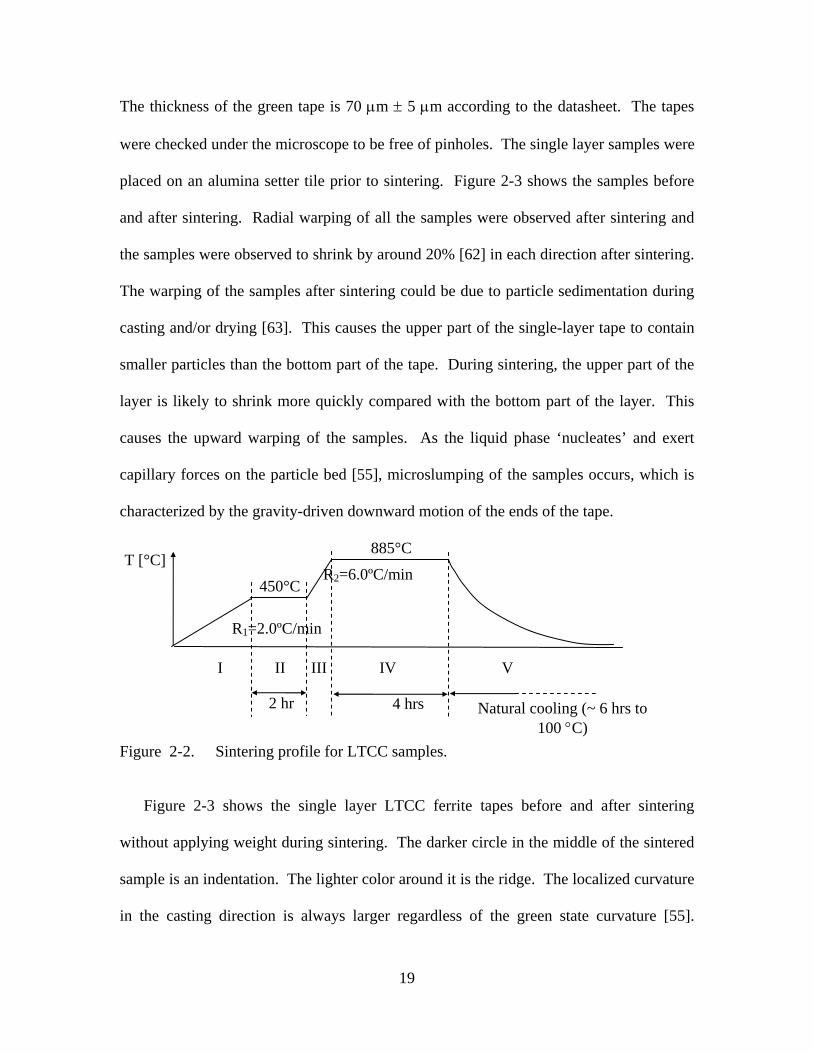
the sintering profile shown in Fig. 2-2, as recommended by Electroscience Labs [62].
19
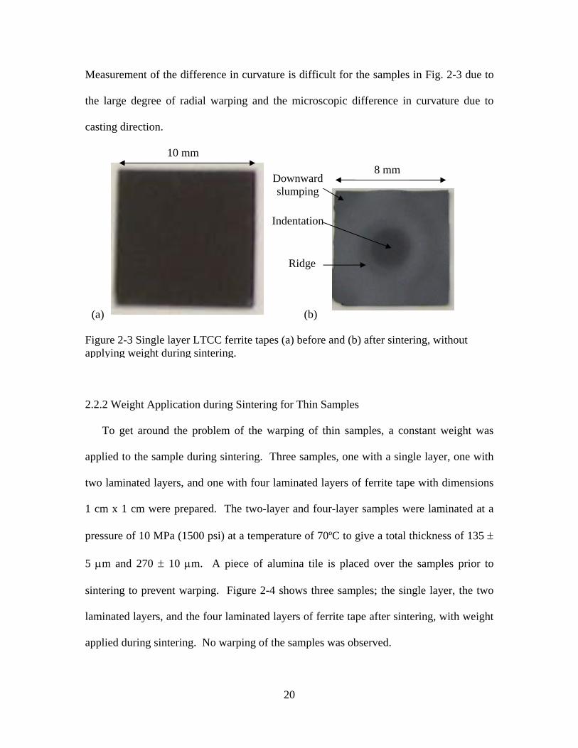
The thickness of the green tape is 70 μm ± 5 μm according to the datasheet. The tapes
were checked under the microscope to be free of pinholes. The single layer samples were
placed on an alumina setter tile prior to sintering. Figure 2-3 shows the samples before
and after sintering. Radial warping of all the samples were observed after sintering and
the samples were observed to shrink by around 20% [62] in each direction after sintering.
The warping of the samples after sintering could be due to particle sedimentation during
casting and/or drying [63]. This causes the upper part of the single-layer tape to contain
smaller particles than the bottom part of the tape. During sintering, the upper part of the
layer is likely to shrink more quickly compared with the bottom part of the layer. This
causes the upward warping of the samples. As the liquid phase ‘nucleates’ and exert
capillary forces on the particle bed [55], microslumping of the samples occurs, which is
characterized by the gravity-driven downward motion of the ends of the tape.
Figure 2-3 shows the single layer LTCC ferrite tapes before and after sintering
without applying weight during sintering. The darker circle in the middle of the sintered
sample is an indentation. The lighter color around it is the ridge. The localized curvature
in the casting direction is always larger regardless of the green state curvature [55].
Figure 2-2. Sintering profile for LTCC samples.
Natural cooling (~ 6 hrs to 100 °C)
450°C
885°C
R1=2.0ºC/min
2 hr 4 hrs
R2=6.0ºC/min T [°C]
I II III IV V
20
Measurement of the difference in curvature is difficult for the samples in Fig. 2-3 due to
the large degree of radial warping and the microscopic difference in curvature due to
casting direction.
2.2.2 Weight Application during Sintering for Thin Samples
To get around the problem of the warping of thin samples, a constant weight was
applied to the sample during sintering. Three samples, one with a single layer, one with
two laminated layers, and one with four laminated layers of ferrite tape with dimensions
1 cm x 1 cm were prepared. The two-layer and four-layer samples were laminated at a
pressure of 10 MPa (1500 psi) at a temperature of 70ºC to give a total thickness of 135 ±
5 μm and 270 ± 10 μm. A piece of alumina tile is placed over the samples prior to
sintering to prevent warping. Figure 2-4 shows three samples; the single layer, the two
laminated layers, and the four laminated layers of ferrite tape after sintering, with weight
applied during sintering. No warping of the samples was observed.
10 mm 8 mm
(a) (b)
Figure 2-3 Single layer LTCC ferrite tapes (a) before and (b) after sintering, without applying weight during sintering.
Indentation
Ridge
Downward slumping

21
In summary, application of weight to thin LTCC ferrite tape samples prior to sintering
prevents warping of the samples.
2.2.3 Application of Alumina powder
Being able to make a mechanically defect-free material is an essential step in
minimizing the complications that may arise from these defects in the material. The
ability to sinter a crack- and dimple-free LTCC material was essential for the more
complex processing which follows. In this set of experiments, a 5.2 cm x 4 cm two-
layered laminated ferrite tape was sintered in air. Another was sintered between alumina
tiles without applying powder on the tiles or on the sample, and two more were sintered
with alumina powder applied on the bottom tile where the sample was placed and on the
upper surface of the sample. For one of the two samples with alumina powder applied, a
non-uniform layer of alumina powder was sprinkled onto the alumina tile prior to placing
the sample onto the tile. For the other sample, a thin layer of powder was applied on the
alumina tile using a blade. The samples were 4.2 cm x 3.2 cm after sintering.
Figure 2-4 LTCC ferrite tape with dimensions of 8 mm x 8 mm after sintering, applying weight during sintering. (a) Single layer, (b) two laminated layers and (c) four laminated layers.
(a) (b) (c)

22
Cracking of the sintered tape was observed, as shown in Fig. 2-5(a), which is
suspected to be due to the downward pressure from the Al2O3 tile used to sandwich the
thin sample. Al2O3 powder was used to alleviate the constraint problem to allow
shrinkage movement of the tape under elevated temperatures. When a non-uniform layer
of Al2O3 powder was applied, dimple formation was observed, as in Fig. 2-5(b), which is
due to the unevenness of the powder applied. However, there was no cracking at the
periphery due to sintering. Finally, when a thin and uniform layer of Al2O3 powder was
applied, there was no cracking nor dimple formation, as shown in Fig. 2-5(c).
In summary, there was cracking at the edges of the thin LTCC sample due to the
friction and constraints imposed by the alumina tiles used to sandwich the sample prior to
sintering. Application of a layer of alumina powder between the sample and the alumina
tiles alleviates this problem. Applying an uneven layer of alumina powder results in
dimpling, which can be avoided by applying a thin and uniform layer of alumina powder
on the samples prior to sintering.
(b) Dimple formation, but no cracking at periphery
(a) Cracking at periphery
Crack due to handling
Dimples
Cracks after sintering

23
2.3 Thick LTCC Ferrite Samples
It has been reported that the curvature of sintered green tape is always larger in the
casting direction, regardless of the green state curvature [55]. To minimize the impact of
casting direction on the camber of the samples, the tapes for the samples are stacked such
that each layer is rotated 90° with respect to the layer below. The tapes are laminated at
the recommended temperature of 70 °C and at the recommended pressure of 10 MPa
(1500 psi) [62]. In this section, the problems of sintering thicker samples are examined.
Solutions to sintering samples of intermediate thickness and thick samples are proposed.
2.3.1 Circumferential cracking of thick samples
Four layers of ferrite tape (25 mm x 25 mm) are laminated at a pressure of 10 MPa
(1500 psi) at a temperature of 70 ºC. Figure 2-6 shows a (a) four-layered sample and (b)
(c) No cracking and no dimple formation
Figure 2-5 Two-layered laminated ferrite tape samples after sintering. (a) Sample sintered between alumina tiles without applying powder on the tiles or sample, (b) samplewith a non-uniform layer of alumina powder applied, (c) sample with a thin layer ofalumina powder applied.

24
eight layered sample after sintering, with weight applied during sintering. Sample (a) has
alumina powder applied and sample (b) does not have alumina powder applied to the
sample prior to sintering. It is observed that both samples have the tendency to fracture
into a circular section during sintering regardless of whether alumina powder is applied.
From this, it can be concluded that application of alumina powder for thin samples
can prevent cracking at the edges of the sample, which is attributed to frictional
constraints imposed by the alumina tiles used to sandwich the sample. Application of
alumina powder for a sample with intermediate thickness, where there are four to eight
layers, or a thick sample of more than eight layers, does not prevent the cracking
problem.
2.3.2 Are circular samples the solution to avoid circumferential cracking?
In this section, circular samples of various thicknesses are fabricated to explore if it is
a solution to avoid circumferential cracking. For magnetic components, there is a
Figure 2-6 LTCC ferrite tape after sintering, when weight was applied during sintering. Sample (a) comprises four layers of laminated LTCC tape and has alumina powder applied. Sample (b) comprises eight layers of laminated LTCC tape and does not have alumina powder applied to the sample.
(a) (b)

25
requirement for sufficient core volume for magnetic energy storage. In view of this
requirement, it is necessary to explore the processing aspect for fabricating thick ferrite
samples. Three circular samples with 4 layers, 10 layers and 20 layers of ferrite tape are
fabricated as shown in Fig. 2-7. The samples have a diameter of 20 mm. No cracking is
observed for the 4-layer and the 10-layer samples. Some circumferential cracking of the
sample is observed for the 20 layer sample. For the 20-layer sample, a higher laser power
is used to cut the sample into a circle. Partial sintering of the peripheral might have
caused the circumferential peeling, as observed in Fig. 2-7(c).
It is of interest to see whether circular samples and samples without sharp edges are
the solution to prevent circumferential cracking for samples with embedded conductor.
Two single conductor inductors are fabricated; a straight conductor inductor, and an
inductor with U-shaped conductor. Twenty layers of ferrite tapes are used for each
sample. Figure 2-8 shows the fabrication procedure of the inductors. The inductor with
the U-shaped conductor is laser cut into a circle. The inductors with the straight
conductor and the U-shaped conductor are sintered with three pieces of alumina tiles on
top to act as weight.
Figure 2-7. Circular samples of diameter 20 mm with (a) 4 layers, (b) 10 layers and (c) 20 layers of ferrite tape. Weight is applied during sintering. .
(a) (b) (c)

26
It is observed that severe cracking of the 20-layered samples occurred for the circular
sample with embedded conductor, as in Fig. 2-8(a), compared to that without an
embedded conductor (see Fig. 2-7(c)). This suggests that gases from the silver paste
exacerbate the cracking problem. This shows that cutting the sample into a circle is not
the best solution for preventing circumferential cracking of thick samples, especially
when conductors are embedded. In addition, fracturing of the samples is observed to
occur at 350-400 ºC, before the binder burnout stage. This suggests that the cracking is
probably due to the forced escape of the gaseous by-products which is inhibited by the
applied weights on top. In addition, the gases from the Ag/Pt paste also contribute to
cracking of the LTCC sample. In the effort to see if elongated samples are possible, a
capsule-shaped sample with rounded corners is fabricated. For the capsule shaped
sample, as shown in Fig. 2-8(b), cracking is also observed.
Figure 2-8 Fabrication procedure of 20-layered samples of LTCC ferrite tape with embedded conductor patterns. (a) Circular sample with U-shaped conductor, (b) capsule-shaped sample with straight conductor applying weight (3 pieces of alumina tile) during sintering.
(b)
(a)
27
From the above experiments, we’ve learned that for thinner samples in which weight
must be applied during sintering, cutting the sample into a circle can help in reducing the
chance of circumferential cracking of the sample. Thicker samples will crack even when
the sample is cut into a circle. The cracking is more severe when a conductor is
embedded. Cracking is due to forced escape of gases before binder burnout, which is
inhibited by the applied weights.
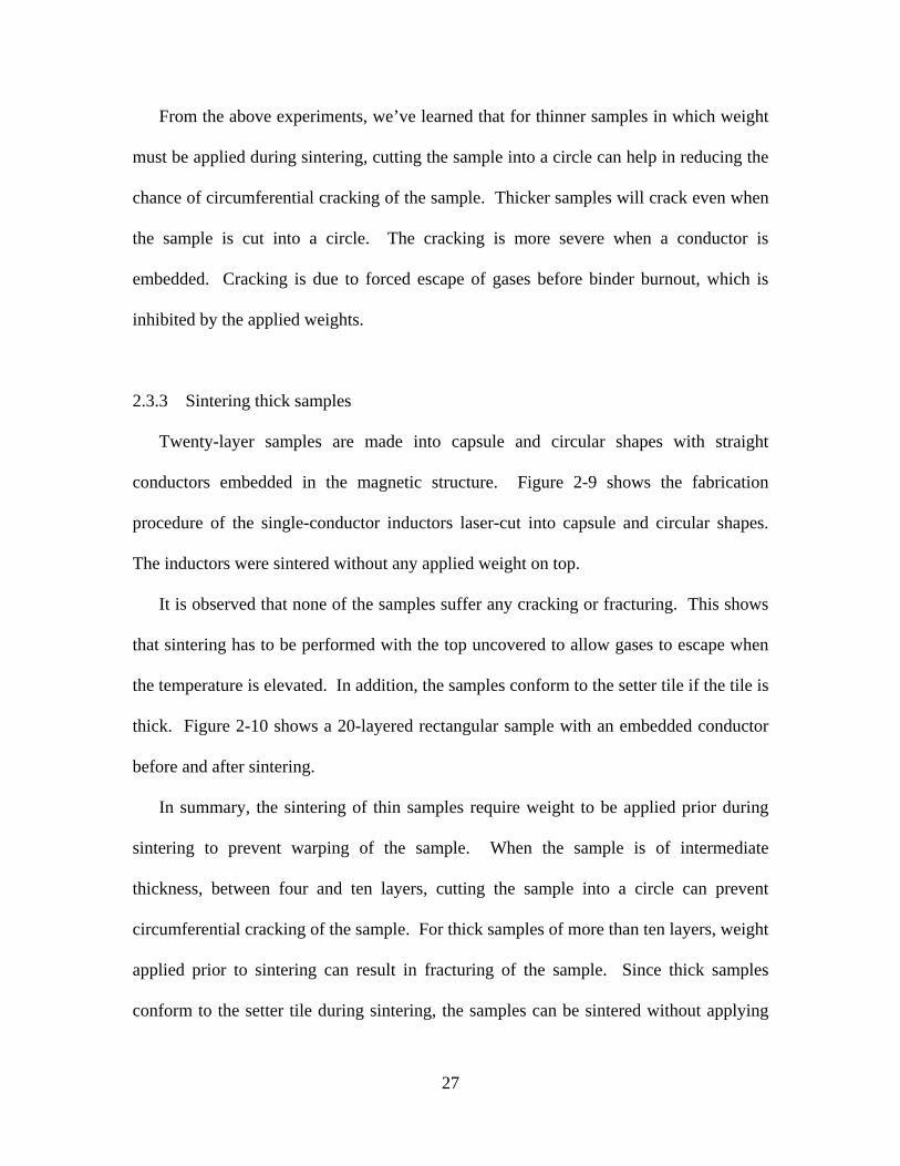
2.3.3 Sintering thick samples
Twenty-layer samples are made into capsule and circular shapes with straight
conductors embedded in the magnetic structure. Figure 2-9 shows the fabrication
procedure of the single-conductor inductors laser-cut into capsule and circular shapes.
The inductors were sintered without any applied weight on top.
It is observed that none of the samples suffer any cracking or fracturing. This shows
that sintering has to be performed with the top uncovered to allow gases to escape when
the temperature is elevated. In addition, the samples conform to the setter tile if the tile is
thick. Figure 2-10 shows a 20-layered rectangular sample with an embedded conductor
before and after sintering.
In summary, the sintering of thin samples require weight to be applied prior during
sintering to prevent warping of the sample. When the sample is of intermediate
thickness, between four and ten layers, cutting the sample into a circle can prevent
circumferential cracking of the sample. For thick samples of more than ten layers, weight
applied prior to sintering can result in fracturing of the sample. Since thick samples
conform to the setter tile during sintering, the samples can be sintered without applying

28
any weight prior to sintering. The first ramp rate (section I in Fig. 2-2) can be lowered to
0.5 °C/min to slow down the escape of gases before the binder burnout process.
Figure 2-10 Twenty-layered rectangular samples of LTCC ferrite tape with embedded conductor (a) before and (b) after sintering.
(b) (a)
Figure 2-9 Fabrication procedure of single-conductor inductors without applying weight during sintering.

29
2.4 Choice of Metallization
The power applications of the end product require an electrical conductivity as high
as possible (which means conduction losses as low as possible) of the metallization. The
choice of the metallization technology for the LTCC process affects the conductivity of
the conductor as well as the cost. However, since the LTCC processing involves
extremely high temperatures, the choice of metal type becomes limited. Copper, an
inexpensive metal with the highest electrical conductivity, is one of the best candidates.
However, since it oxidizes at elevated temperatures, it may not be the best choice to be
used with LTCC. In this section, the possibility of using copper with LTCC will be
evaluated.
2.4.1 Possibility of Using Copper with LTCC
In this section, samples are sintered at various ambients to observe their effect on
sintering. The three sintering ambients used are: (a) oxidizing ambient (air), (b) reducing
ambient (H2/N2), and (c) inert ambient (Ar). Three samples are made, which comprise a
strip of copper sandwiched between two layers of ferrite tape and laminated at a pressure
of 10 MPa (1500 psi) and at a temperature of 70 °C. Figure 2-11 shows a drawing of the
samples. Figure 2-12 shows the samples sintered in the three ambients.
The copper in the sample sintered in air has been oxidized, as seen in Fig. 2-12 (a).
For the samples sintered in the reducing ambient, the copper remains un-oxidized, but
reduction of the ferrite into metallic iron is observed, as shown in Fig. 2-12(b). The
sample becomes silver in color and shows conductive behavior when tested with a

30
multimeter. For the sample fired in an inert ambient, as in Fig. 2-12(c), the copper
remains in tact, but the ferrite tape is observed to be black, as opposed to becoming gray,
which is characteristic of ferrite, after sintering.
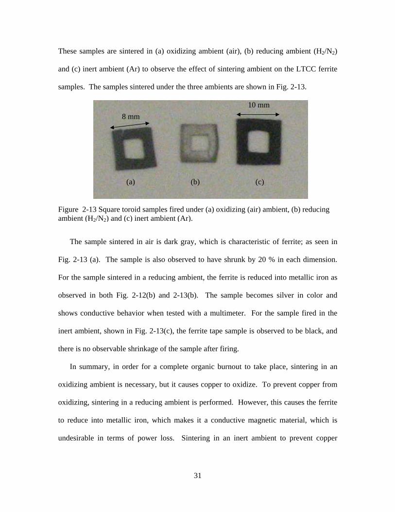
To investigate the effect of sintering ambient on the ferrite tape itself, another three
samples are fabricated. The samples are square toroids. Eight layers of ferrite tape are
laminated at a pressure of 10 MPa (1500 psi) and at a temperature of 70 °C. The samples
are cut into 10 mm x 10 mm squares with a 5 mm x 5 mm square hole in the middle.
Figure 2-11 Drawing of sample with copper strip sandwiched between two layers of ferrite tape.
Copper strip
LTCC Ferrite tape
Figure 2-12 Samples of copper strip sandwiched in two layers of ferrite tape fired under(a) oxidizing (air) ambient, (b) reducing ambient (H2/N2) and (c) inert ambient (Ar).
(a) (b) (c)
Oxidized copper
Copper strip
31
These samples are sintered in (a) oxidizing ambient (air), (b) reducing ambient (H2/N2)
and (c) inert ambient (Ar) to observe the effect of sintering ambient on the LTCC ferrite
samples. The samples sintered under the three ambients are shown in Fig. 2-13.
The sample sintered in air is dark gray, which is characteristic of ferrite; as seen in
Fig. 2-13 (a). The sample is also observed to have shrunk by 20 % in each dimension.
For the sample sintered in a reducing ambient, the ferrite is reduced into metallic iron as
observed in both Fig. 2-12(b) and 2-13(b). The sample becomes silver in color and
shows conductive behavior when tested with a multimeter. For the sample fired in the
inert ambient, shown in Fig. 2-13(c), the ferrite tape sample is observed to be black, and
there is no observable shrinkage of the sample after firing.
In summary, in order for a complete organic burnout to take place, sintering in an
oxidizing ambient is necessary, but it causes copper to oxidize. To prevent copper from
oxidizing, sintering in a reducing ambient is performed. However, this causes the ferrite
to reduce into metallic iron, which makes it a conductive magnetic material, which is
undesirable in terms of power loss. Sintering in an inert ambient to prevent copper
Figure 2-13 Square toroid samples fired under (a) oxidizing (air) ambient, (b) reducing ambient (H2/N2) and (c) inert ambient (Ar).
(a)
(b)
(c)
10 mm 8 mm

32
oxidation also proves to be unsatisfactory as this prevents the organic binder burnout
process due to the lack of oxygen, though copper oxidation is avoided.
2.4.2 Reduction of copper oxide to copper
A possible solution to counteract the copper oxidation problem is to first conduct the
sintering in air to allow organic burnout to take place. After the sintering step, copper
oxide can be reduced back to copper in a reducing ambient, at a lower temperature to
slow down the process of ferrite reduction.
A strip of copper laminated with ferrite tape on both sides was sintered in air at 885
°C. After cooling down to room temperature, the samples were then placed in a reducing
ambient, H2/N2, and the temperature raised to 350 °C for one hour. Figure 2-14 shows
the sintering profile, consisting of the organic burnout, densification and reducing step.
A cross-sectional view of the copper after oxidation and reduction is studied and
compared. Figure 2-15 shows the cross-sectional view of copper (a) before oxidation, (b)
after oxidation, and (c) followed by subsequent reduction.
From Fig. 2-15(b), it is observed that after the copper is oxidized, it increases in
volume. This causes the ferrite tape surrounding the copper to be under tensile stress.
Cracking and delamination of the ferrite tape at the edges of the copper may result, as
shown in Fig. 2-15(b). It is also observed that after copper oxide is reduced back to
copper it does not shrink back to its original volume. This suggests an increased in
overall porosity of the copper after reduction and a possible reduction in the conductivity
of copper, which underwent a redox reaction.

33
(b)
Sample holder
Sample holder
Oxidized copper
Sintered ferrite tape
Crack
Figure 2-14 Sintering profile conducted in air followed by reducing profile conducted in H2/N2.
450°C
885°C
R1=2.0ºC/min
2 hr 4 hrs Natural cooling (~6 hrs to 100 °C)
R2=6.0ºC/minT [°C] 350°C
H2/N2
R3=2.0ºC/min
Binder burnout Densification
1 hr
Air
Reduction
time
(a)
Copper Ferrite tape
Sample holder
Sample holder
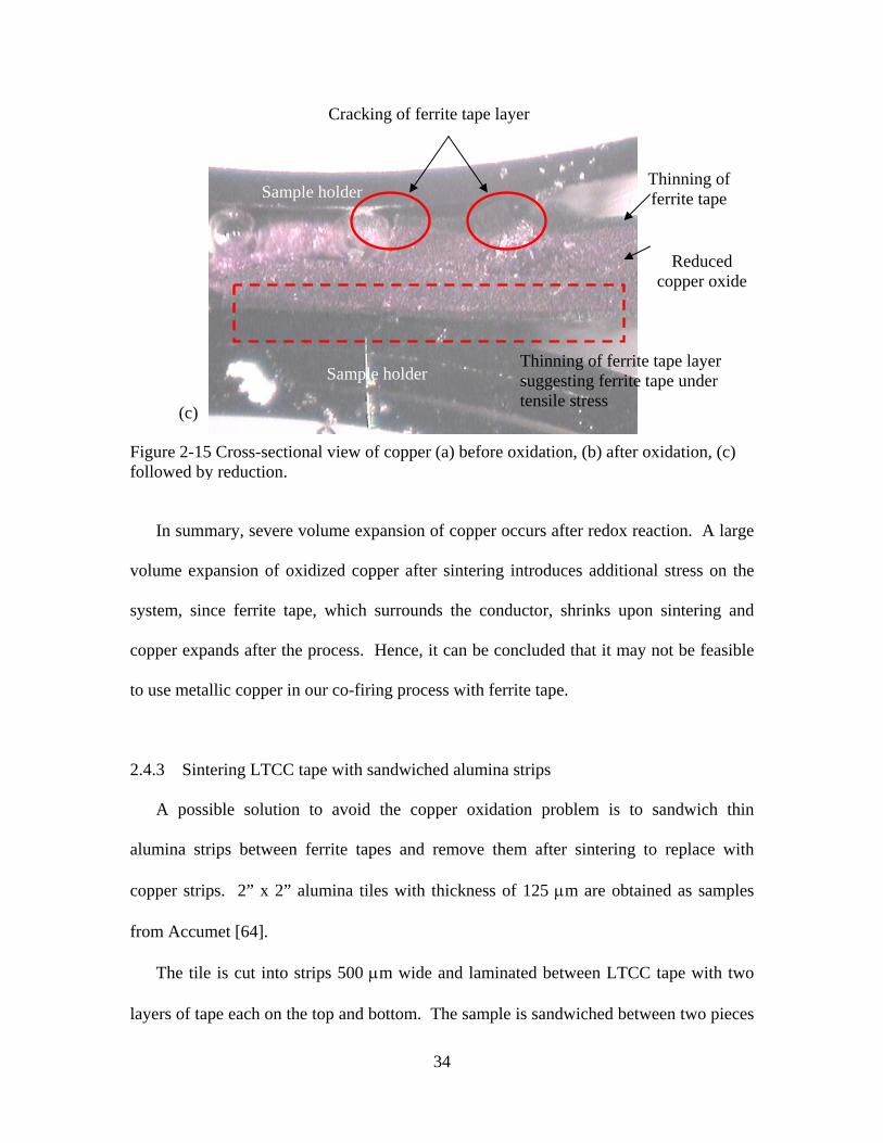
34
In summary, severe volume expansion of copper occurs after redox reaction. A large
volume expansion of oxidized copper after sintering introduces additional stress on the
system, since ferrite tape, which surrounds the conductor, shrinks upon sintering and
copper expands after the process. Hence, it can be concluded that it may not be feasible
to use metallic copper in our co-firing process with ferrite tape.
2.4.3 Sintering LTCC tape with sandwiched alumina strips
A possible solution to avoid the copper oxidation problem is to sandwich thin
alumina strips between ferrite tapes and remove them after sintering to replace with
copper strips. 2” x 2” alumina tiles with thickness of 125 μm are obtained as samples
from Accumet [64].
The tile is cut into strips 500 μm wide and laminated between LTCC tape with two
layers of tape each on the top and bottom. The sample is sandwiched between two pieces
Figure 2-15 Cross-sectional view of copper (a) before oxidation, (b) after oxidation, (c) followed by reduction.
(c)
Cracking of ferrite tape layer
Thinning of ferrite tape layer suggesting ferrite tape under tensile stress
Thinning of ferrite tape
Sample holder
Sample holder
Reduced copper oxide

35
of silicone rubber pads during laminating to improve the distribution of pressure on the
sample, since the surface of the sample is uneven due to the presence of the alumina strip.
The samples with sandwiched alumina strips are sintered in air with the sintering profile
shown in Fig. 2-2. Figure 2-16 (a) shows the samples before sintering, and Fig. 2-16 (b)
shows the samples after sintering. Figure 2-17 shows the cross-sectional view of a post-
sintered sample with the alumina strip sandwiched between layers of ferrite tape.
In Fig. 2-16 (b) fracturing of the LTCC tape at the edges parallel to the alumina strips
is observed, which is due to constrained shrinkage of the LTCC tape. The alumina strips
are observed to adhere strongly to the sintered tape. In Fig. 2-17, fracturing of the LTCC
tape at the edges is observed under a microscope. This is attributed to stresses developed
during sintering, when the LTCC tape shrinks and the alumina strip does not change in
Figure 2-17 Cross-sectional view of a thin alumina strip sandwiched in LTCC ferrite tape after sintering.
Crack
alumina Ferrite tape
Figure 2-16 Thin alumina strips sandwiched in LTCC ferrite tape (a) before and (b) after sintering.
(b) (a)
Alumina strips Alumina strips
LTCC ferrite tape

36
volume. Hence, sandwiching thin alumina strips between ferrite tapes and removing
them after sintering to replace with copper strips may not be feasible.
2.4.4 Using Copper Paste
Copper paste designed for thick-film printing can be purchased from Electroscience
Labs. The recommended firing temperature is 900 ºC to 980 ºC in a nitrogen sintering
ambient, with optimum performance achievable by firing at 980 ºC. However, this
temperature is 100 ºC higher than the recommended sintering temperature of the LTCC
ferrite tape. In addition, the resistivity of the copper after sintering is less than half that
of elemental copper due to the presence of additives and glass included in the paste.
Figure 2-18 shows the sheet resistance of such printed copper paste vs. fired thickness
[65]. The conductivity of the sintered copper paste ranges from 25 to 34 MS/m, which is
around half the conductivity of elemental copper.
Figure 2-18 Sheet resistance of sintered copper paste vs. fired thickness [65].
Res
istiv
ity [m
Ω/s
q]

37
Due to the complexity in the sintering process of copper paste, which requires
sintering in an inert ambient, as well as the difference in sintering temperature between
the copper paste and the LTCC ferrite tape, we must seek other options in the choice of
metallization.
2.4.5 Using Ag/Pt Paste
In section 2.4.2 it is concluded that the volume expansion of copper after sintering
resulted in severe tensile stress in the ferrite tape, which shrinks after sintering. This
difference in sintering behavior makes copper a less compatible conductor with the
LTCC processing technique. In this section, experiments using Ag/Pt paste conductors
purchased from Electroscience Labs with the LTCC ferrite tape are reported. The Ag/Pt
paste has a recommended sintering temperature of 875 ºC [66], which is very close to that
of LTCC ferrite tape (885 ºC), which can ensure co-firing compatibility with the LTCC
ferrite tape.
To test the compatibility of the Ag/Pt paste with LTCC ferrite tape, the conductor
paste is screen-printed onto a layer of LTCC ferrite tape. The conductor is dried at 70 °C
for one hour. Two layers of LTCC ferrite tape are placed on top and one layer is placed
on the bottom of the LTCC ferrite tape sample with a printed conductor pattern. The
sample is laminated at 70 °C at a pressure of 10 MPa (1500 psi), forming a structure with
embedded conductors. The sample is sintered using the sintering profile in Fig. 2-2.
Figure 2-19 shows the cross-sectional view of the sample after sintering. No sign of
cracking is observed, as opposed to the cracking and thinning of ferrite tape observed
when copper is used as the metallization, as shown in Fig. 2-15(c).

38
In terms of processing, the ESL 953 Ag/Pt paste is compatible to process with the
LTCC ferrite tape, since their recommended co-firing temperatures are very close to each
other. Experimental results of co-firing the Ag/Pt paste with LTCC ferrite tape shows no
signs of cracking, delamination or thinning of the LTCC tapes.
2.4.6 Alternative cross-sectional shapes for conductors
In the development of a fabrication process suitable for power applications, several
essential points must be taken into account, such as the choice of magnetic material for
the targeted application, flexibility in the design, and manufacturing of an inductor with
low conduction losses. The conventional method of screen-printing conductor paste on
LTCC green tape proves to be unsuitable for power applications due to the limitation in
the conductor’s cross-sectional area and cross-sectional shape [67], as illustrated in Fig.
2-19. The presence of sharp edges would lead to high current densities at these edges,
which will result in elevated conduction losses. The situation is aggravated when the
conductors are embedded in a magnetic medium. The next section elaborates on the
Figure 2-19 Cross-sectional view of screen-printed Ag/Pt conductors embedded in LTCC tape after sintering.
Ag/Pt paste
LTCC ferrite tape

39
LTCC power inductor fabrication procedure to form conductors with better-shaped and
larger cross-sectional area.
2.4.7 Power Inductor Fabrication Procedure
2.4.7.1 Single Conductor Inductor
The materials used for inductor fabrication are LTCC ferrite green tape2 and
silver/platinum (Ag/Pt) paste3 purchased from Electroscience Labs [28]. First, the LTCC
ferrite tapes are cut into rectangles. Several layers of the rectangular LTCC ferrite tapes
are laminated to form the top, middle, and bottom main layers. The tapes are laminated
using a hydraulic lab press. The laminating temperature is 70 ºC and the pressure is 10
MPa (1500 psi). A slot is cut in the middle main layer using a Class IV 100 W CO2 laser
cutting machine. Two smaller slots 21 mm apart are laser-cut in the top main layer.
Figures 2-20(a) and 2-20(b) are photographs of the bottom and middle main layers after
the laser cutting step.
The main middle layer is placed on top of the bottom main layer and subsequently
laminated at a temperature of 70º C, with a pressure of 10 MPa (1500 psi), as shown in
Fig. 2-20(c). Next, Kapton tape is adhered to the structure, and the part of the Kapton
tape that lies above the indented slot is removed using an X-acto knife, exposing the slot.
Ag/Pt conductor paste is then wiped into the slot using a 6 cm × 4 cm × 0.6 cm silicone
rubber squeegee. The Kapton tape layer serves to protect the underlying LTCC ferrite
2 LTCC ferrite green tape – part number ESL-40010 3 Ag/Pt paste – part number ESL-953
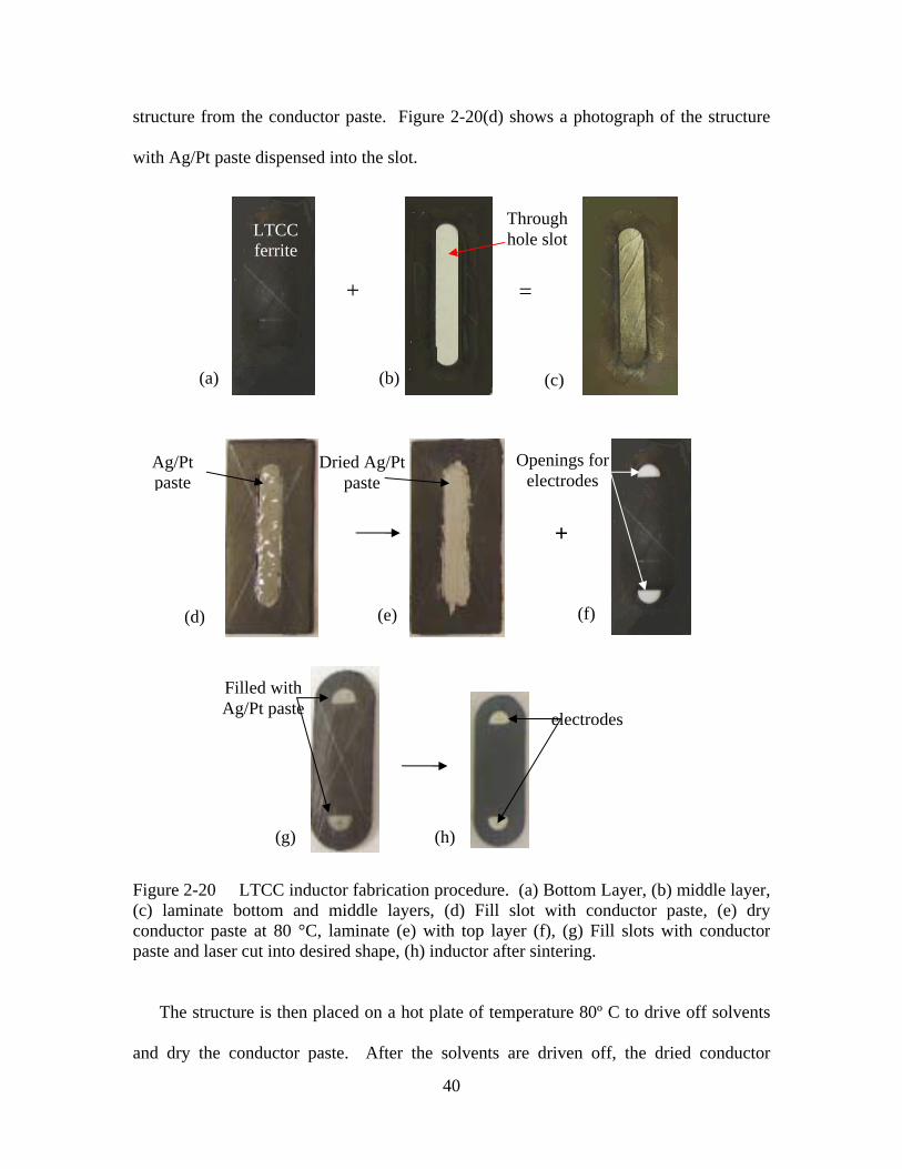
40
structure from the conductor paste. Figure 2-20(d) shows a photograph of the structure
with Ag/Pt paste dispensed into the slot.
The structure is then placed on a hot plate of temperature 80º C to drive off solvents
and dry the conductor paste. After the solvents are driven off, the dried conductor
(g) (h)
Figure 2-20 LTCC inductor fabrication procedure. (a) Bottom Layer, (b) middle layer, (c) laminate bottom and middle layers, (d) Fill slot with conductor paste, (e) dry conductor paste at 80 °C, laminate (e) with top layer (f), (g) Fill slots with conductor paste and laser cut into desired shape, (h) inductor after sintering.
Filled with Ag/Pt paste electrodes
+
(a) (b) (c)
=
Through hole slotLTCC
ferrite
Ag/Pt paste
(d) (e) (f)
+
Dried Ag/Pt paste
Openings for electrodes

41
decreases in volume, resulting in vertical shrinkage. The process of wiping the conductor
paste into the slot is then repeated four to five times until the dried conductor paste is
almost level with the ferrite layers at its peripherals. Then the Kapton tape is removed.
Figure 2-20(e) shows the structure after the conductor dries.
Next, the top main layer, shown in Fig. 2-20(f), is laminated on top of the structure
shown in Fig. 2-20(e). Conductor paste is then dispensed into the two small slots, which
will form the pads for the electrodes for external connection. It is then laser-cut into the
desired size and shape, as shown in Fig. 2-20(g). The structure is then sintered in a
normal atmosphere using the VULCAN 3-550 sintering oven, as per Fig. 2-21. A
photograph of the fabricated inductor is shown in Fig. 2-20(h). Due to the large thickness
of the LTCC tape layers and the conductor paste, the first ramp rate of the sintering
profile from room temperature to the binder burnout temperature is lowered to 0.5
°C/min.
450°C
885°C
R1=0.5ºC/min
2 hr 4 hrs Natural cooling (~ 6 hrs to 100 °C)
R2=6.0ºC/min T [°C]
time I II III IV V
Figure 2-21 Sintering profile for LTCC inductor samples with reduced 1st ramp rate (region I).

42
2.4.7.2 Multi-Conductor Inductor
The fabrication of the multi-conductor inductor is similar to that of the single
conductor inductor. For the middle main layer, the respective number of slots is cut, as
similar to the step shown in Fig. 2-20(b). The middle main layer is then laminated with
the bottom main layer. The ends of the thin strips which separate the individual slots are
removed using an X-acto knife, as illustrated in Fig. 2-22 (a). Subsequently, conductive
paste is dispensed into the slots and dried at 80 ºC to drive off solvents. The procedure of
dispensing conductive paste is repeated four to five times, similar to that of the single
conductor inductor. Figure 2-22(b) shows the samples with slots filled with dried
conductive paste.
(a) Formation of indented slots.
Thin strips separating slots
End of thin strip removed by X-acto
knife
(b) Dispensing of conductor paste.
Thin strips separating slots

43
Next the top main layers are laminated with the structures shown in Fig. 2-22(b),
resulting in Fig. 2-22(c). Conductor paste is then dispensed into the exposed slots, which
form the pads for the electrodes for external connection. The samples are then laser-cut
into the desired size and shape and sintered in a normal atmosphere in the sintering oven
and following the sintering profile of Fig. 2-21. The photograph of the fabricated
inductors is shown in Fig. 2-22(d).
2.4.8 Conductivity and Solderability Improvement
The addition of glass and other additives into the silver paste results in the lowering
of the conductivity of the sintered silver. Measurements of the conductivity of the
(c) Laminating top layer, exposing inductor electrodes.
(d) After sintering.
n=1 n=2 n=3
Figure 2-22 Fabrication procedure for multi-conductor inductor with number of parallel conductors, n = 1 to 3.

44
sintered Ag/Pt paste will be elaborated in Chapter 3 of the dissertation. The external
metallization of the component can be electroplated with copper to improve the
solderability of the sintered Ag/Pt paste and to improve the contact resistance [67]. Fig.
2-23 shows a multi-conductor inductor sample with electroplated copper electrodes.
Electroplating the contacts with copper reduces the contact resistance of the sample.
The overall resistance is reduced from 36 mΩ to 15 mΩ as measured by a DC ohmmeter.
Parasitic contact resistance is especially crucial for inductors with low inductance values
and low dc resistance values.
2.5 Conclusions for Chapter 2
The application of weight to thin LTCC ferrite tape samples prior to sintering
prevents warping of the samples. Application of a thin layer of alumina powder
alleviates cracking at the edges of LTCC samples of fewer than three layers, which is due
to the friction and constraints imposed by the alumina tiles which are used to sandwich
the samples prior to sintering. Applying an uneven layer of alumina results in dimpling,
Figure 2-23 Electrodes of inductor electroplated with copper to improve solderability.
Plated copper LTCC ferrite

45
which can be avoided by applying a thin and uniform layer of alumina powder on the
samples prior to sintering.
For thin samples in which weight must be applied during sintering, cutting the sample
into a circle can help reduce the chance of circumferential cracking of the sample. For
thicker samples greater than seven layers, samples will still crack even when the sample
is cut into a circle, which is due to the forced escape of gases, which is inhibited by the
applied weights. For thick samples, weight does not need to be applied prior to sintering
since thick samples conform to the setter tile during sintering. The first temperature ramp
rate between room temperature and the binder burnout temperature can be lowered to
allow for a slow release of gases before the binder burnout process.
For complete organic burnout to take place, sintering the LTCC ferrite tape samples
in an oxidizing ambient is necessary, which makes the use of copper with the LTCC
process less attractive. Sintering in a reducing ambient to prevent copper oxidation
causes ferrite to reduce into metallic iron. Sintering in an inert ambient to prevent copper
oxidation prevents the organic binder burnout process. Severe volume expansion of
copper occurs after oxidation, which introduces additional stress on the system, since the
ferrite tape surrounding the conductor shrinks upon sintering and copper expands after
the process. After subsequent reduction, the copper does not shrink to its original
volume. In view of the inherent stress caused by co-firing copper with LTCC ferrite tape
and the complexity involved in the requirement of different ambients for sintering LTCC
ferrite tape and copper, it can be concluded that it is not feasible to employ copper
metallization in our co-firing process with ferrite tape.

46
In terms of processing, Ag/Pt paste ESL 953 is compatible for processing with LTCC
ferrite tape, since the recommended co-firing temperatures of the two tapes are very
close. Experimental results of co-firing the Ag/Pt paste with LTCC ferrite tape does not
show signs of cracking, delamination, thinning or gapping of the LTCC tapes.
Electroplating the contacts with copper reduces the contact resistance of the sample and
helps improve solderability.

47
Chapter 3. LTCC – Material Characterization for Power Magnetics
3.1 Overview
Material characterization is an important step in understanding the properties of the
materials used for magnetics integration. In the beginning of this chapter, the dielectric
property, in the form of permittivity of the LTCC ferrite tape used for magnetics
integration, will be discussed. The major focus of this chapter is on the magnetic
characterization of the LTCC ferrite tape discussed in Chapter 2. The various sources of
error in core loss measurement are identified and analyzed. Subsequently, the operational
influence on electromagnetic characteristics of the LTCC magnetic material, will be
explored. The effect of frequency, temperature and pre-magnetization on the
electromagnetic characteristics of the LTCC magnetic material will be examined.
Finally, a core loss model based on the Steinmetz equation, with temperature and pre-
magnetization dependence will be developed. Effect of the temperature and the DC pre-
magnetization on the Steinmetz exponents is also studied. Finally, the conductive paste
used for forming the windings of the magnetic component is electrically characterized.
3.2 Estimation of Permittivity
Several methods of permittivity measurement have been reported. The dielectric rod
resonator method [68] is commonly used to measure the dielectric properties of high
permittivity and low loss dielectric materials in the microwave region. In [69], a non-

48
contact microwave probe is used to observe high frequency microscopic dielectric
distributions in the cross-section of a multi-layer ceramic capacitor. The reflection
intensities obtained were transformed into dielectric permittivity, which enables
measurement of local dielectric property. In [70], a coaxial probe and in [71], a cavity
perturbation technique have been used for permittivity measurements. The above
techniques are suitable for dielectric characterization of materials in the RF and
microwave region.
In this dissertation, permittivity of the ferrite tape is measured by sandwiching the
ferrite tape between two conductive layers to form a single layer capacitor structure. The
impedance characteristic is measured using the 4294A impedance analyzer, from which
the capacitance and the relative permittivity are obtained.
3.2.1 Sample Preparation
Samples of 1cm x 1cm squares were cut from a ferrite tape. Four layers of the tape
were laminated at a pressure of 10 MPa (1500 psi) and at a temperature of 70 °C. A
square hole, 0.8 cm x 0.8 cm is cut in a piece of kapton tape, which serves as the stencil
for printing conductive paste onto the ferrite tape samples. The cut square of the kapton
tape stencil is aligned in the center of the ferrite tape squares. Ag/Pt paste is stencil
printed onto the ferrite tape squares using a spatula. The sample is dried in air at a 70 °C
for 1 hour. The process of stencil printing conductive paste onto the ferrite square and
drying is repeated on the reverse side.

49
The sample is placed on a bed of alumina powder coated alumina tile to prevent the
Ag/Pt paste from adhering to the alumina tile. Another piece of alumina powder coated
alumina tile is placed on top of the sample to prevent warping of the thin sample. The
sample is sintered in air. After sintering, the sample shrunk to 0.8 cm x 0.8 cm. Copper
strips are soldered onto the Ag/Pt pads to form external contacts for impedance
measurement. Fig. 3-1 shows a capacitor sample for dielectric constant estimation. The
silver pads were estimated to be 6.5 mm x 6.5 mm. Two such capacitors have been
fabricated for this set of measurements.
3.2.2 Permittivity Measurement
The impedance characteristics of the samples are measured using the Agilent 4294A
impedance analyzer. Fig. 3-2 shows the plot of admittance (Y) vs. frequency. Using |Y|
= 2πC.f, where C is the capacitance and f is the frequency, C is estimated to be 19.4pF
and 21.8pF from the gradient of the Y vs. f plot, as shown in Fig. 3-2. Using the equation:
Figure 3-1 Capacitor samples for dielectric constant estimation.
6.5 mm
6.5 mm
Ag/Pt pad
LTCC ferrite
8 mm
8 mm
Copper strap

50
dA
C r 0εε= ,
where
εr : dielectric constant
ε0 : permittivity of free space
A : surface area of conductor
d : thickness of ferrite layer
the thickness of the ferrite layer, d = 237.5μm, the surface area of the conductor, A = 0.65
x 0.65 cm2 and the above calculated capacitance values, the dielectric constants were
estimated to be 12.3 and 13.8 respectively. The average dielectric constant of the ferrite
tape is taken to be approximately 13.
0
5
10
15
20
0 20 40 60 80 100frequency (MHz)
Adm
ittan
ce (m
S)
Figure 3-2 Graph of admittance vs. frequency for the two parallel plate capacitor samples.
Y = 1.22 x 10⁻¹⁰ f
Y = 1.37 x 10⁻¹⁰ f
(3-1)

51
3.3 Estimation of Core Loss
Numerous core loss characterization techniques have been reported in literature.
Core loss can be quantified electrically or by calorimetric means [72]. In electrical
characterization of core loss, impedance measurement method [73-75], the CEEC 25300
or CEEC 25000 method [76], or other electrical methods [77] can be applied. In [78], an
electrical method is used to characterize core loss of an inductor in a conventional buck-
boost converter. An analysis of amplitude and phase shift errors in measurement is made
and presented mathematically. In this section, the various sources of error is identified
and analyzed in the variation of the European standard CECC25300 or CECC25000 [76]
method of characterizing core loss.
3.3.1 Circuit for Loss Measurement
In the measurement of core loss, due to the low permeability of the material and the
limited driving capability of the power amplifier used, a capacitor is connected in parallel
with the primary windings of the circuit, similar to the European standard CECC 25300
[76], to provide a parallel resonant peak at the frequency of interest. Fig. 3-3 shows the
core loss measurement circuit. R is the current sense resistor to sense the current in the
primary windings. C1 is the parallel resonant capacitor. C2 is the DC blocking capacitor.
L1 is an AC choke.

52
3.3.2 Components in Circuitry for Loss Measurement
The LTCC technology for magnetics integration, which is being explored in this
dissertation, is targeted at integrating magnetics in small, high power density point-of-
load (POL) converters. The technology limits possible sample sizes for core loss
measurement. In the measurement of core loss, due to the small size of the magnetic
core, low permeability of the material and the limited driving capability of the power
amplifier used, a slight modification is made to the circuit similar to the European
standard CECC 25300 [76] to accommodate to the above mentioned limitations. A
capacitor is connected in parallel with the primary windings of the circuit to provide a
parallel resonant peak at the frequency of interest to increase the voltage drop across the
primary windings as well as to provide current to the primary windings of the
transformer.
In the core loss measurement circuit shown in Fig. 3-3, AC excitation is provided by
means of a function generator Agilent 33220A. The AC source is connected to a 25 W
RF amplifier from Amplifier Research, of model 25A250A. This constitutes the AC
Figure 3-3. Core loss measurement circuit.
RVDC
C1
P1
P2
S1
TX1C2
V1
L1
I
- VR + V2 +
-
N1 : N2

53
source V1 as shown in Fig. 3-3. VDC is provided by means of a DC power supply from
Lambda, of model UP6-132. C2 is a DC blocking capacitor, C1 is a parallel resonant
capacitor to produce a parallel resonant peak at the frequency of interest. R is a current
viewing resistor in which the voltage across the resistor is measured to obtain the current.
L1 is an AC choke to reduce the effect of AC perturbation from the primary windings, P1.
P2 is the DC windings and S1 is the secondary windings. The induced voltage, V2, is
measured across the open circuited secondary windings.
3.3.2.1 Toroidal Core for Loss Measurement
The technology for integrating magnetics in small, high power density point-of-load
(POL) converters limits possible sample sizes for core loss measurement. In the
measurement of core loss, a bicycle-wheel-like toroidal core made from LTCC ferrite
tape is fabricated. The magnetic flux density is approximated to be a constant within the
cross-sectional area of the core due to its large radius to core width ratio.
A. Core Design.
In the design of the core dimensions, it is necessary to take into account the power
loss for reasonably accurate measurements at low frequency and low magnetic flux
densities, effect of non-uniform flux densities on core loss characterization, mechanical
and structural reliability of the component under test. To obtain a more uniform flux
density distribution, it is desirable to use a core with inner radius close to the outer radius.
However, this may pose problems when it comes to the mechanical strength of the core to
withstand the stress from wires wound around it. To obtain a more reliable measurement

54
data, larger power loss is desired, especially at low frequencies and low magnetic flux
densities. Hence, the core has to have a volume large enough to ensure measurable losses
at low power loss conditions and small enough to be driven by the available power
amplifier.
The basic Steinmetz equation [79] is given by:
βα BfKP pv ⋅⋅= (3-2)
where
Pv – specific core loss
f - frequency,
B – magnetic flux density
α, β, – Steinmetz exponents
Kp – Constant
Using (3-2) and assuming f to be a constant, βBPv ∝ . Assuming the magnetic flux
density, B, is constant throughout the toroidal core, the power loss, P1, can be expressed
as:
][ 221 io rrhBP −∝ πβ (3-3)
where
h – thickness of the core
ro – outer radius of the core
ri – inner radius of the core

55
For non-uniform B in a toroidal core, power loss, P2, can be expressed as:
][)2
(22 22
2βββ
πμ
βπ −− −−
∝ io rrnihP (3-4)
where
μ - magnetic permeability
n – number of turns
i - current
The average magnetic flux density, Bavg, can be expressed as:
io
ioavg rr
rrniB−−
⋅=)ln()ln(
2πμ (3-5)
The derivation for (3-3), (3-4) and (3-5) can be found in Appendix.
The specific core loss, assuming uniform magnetic flux density, is given by:
)( 221
1io
v rrhP
P−
=π
(3-6)
The specific core loss assuming non-uniform magnetic flux density is given by:
)( 222
2io
v rrhP
P−
=π
(3-7)
The % error in specific core loss is:
%100%2
12 ×−
=v
vv
PPP
error (3-8)
Figure 3-4 shows the graph of % error in Pv as a function of the ratio of inner radius
to outer radius, o
i
rr
. For o
i
rr
> 0.7, and assuming β to be 2.2, the error in power loss
estimation assuming B as a constant, is less than 1 %. It is of interest to see what is the %

56
error in Pv when β varies. Figure 3-5 shows the graph of % error in Pv vs. β for o
i
rr
= 0.5,
0.75 and 0.9. It is observed that for the % error in Pv to be less than 1 % for β in the
range of 1 to 3, o
i
rr
has to be greater than 0.75 (see Fig. 3-5).
-2
0
2
4
6
1 1.5 2 2.5 3 3.5
beta
% e
rror i
n P
v
0.5
0.75
0.9
Figure 3-5. Percentage error in specific core loss vs. β for ri / ro = 0.5, 0.75 and 0.9.
ri / ro
1
β
Figure 3-4. Percentage error in specific core loss vs. ri / ro.
0
2
4
6
8
10
12
0 0.2 0.4 0.6 0.8 1ri/ro
% e
rror i
n P
v

57
From measurement results of 4F1 [80] core material, the Steinmetz exponents are
estimated to be α = 1.08, β = 2.07, Kp = 0.001947. Using these values, the power loss in
the core can be estimated. The maximum power loss is designed to be at f = 4 MHz and
Bm = 50 mT. Choosing o
i
rr
=0.8 and core thickness, h, to be 2 mm, the graph of power
loss vs. ro can be plotted as shown in Fig. 3-6.
The power rating of the power amplifier of model AR 25A250A is 25 W. To give
some headroom for other losses and inaccuracies in the assumptions of the Steinmetz
exponents, the dimensions of the core is chosen such that the power loss is less than 20
W. Hence, the core dimensions are chosen to be ir = 10 mm, or = 12.5 mm, h = 2 mm.
B. Core Fabrication
In the fabrication of the toroidal core, 42 layers of LTCC tape of dimensions 3.5 mm
x 3.5 mm are stacked and laminated as described in Chapter 2.3. Concentric circles of
diameter 31.25 mm and 25 mm are subsequently cut on the sample using laser
0
5
10
15
20
25
10 11 12 13 14 15ro [mm]
Pow
er lo
ss [W
]
Figure 3-6. Power loss vs. ro, for ri / ro = 0.8 and h = 2 mm.
ri / ro = 0.8

58
machining. The cut samples are then placed on an alumina setter tile and sintered in an
oven using the sintering profile in Fig. 2-21. Table 3-1 tabulates the toroidal core’s
dimensions after sintering. Fig. 3-7(a) shows the top view of the geometry of the toroidal
core. Fig. 3-7(b) shows the cross-sectional view. Fig. 3-8 shows the photograph of the
toroidal core for loss measurement. Table 3-2 tabulates the total core cross-sectional
area, volume and average magnetic path length of the core.
Table 3-1 Core Dimensions.
OD [mm] ID [mm] h [mm]
Before sintering 31.40 24.90 2.65
After sintering 25.08 19.94 2.12
OD
ID
w w
h h
Figure 3-7 Geometry of toroidal core. (a) Top view, (b) cross-sectional view.
(a)
(b)

59
Table 3-2 Total Core Dimensions.
Cross-sectional area [mm2] 5.444
Volume [mm3] 384.9
Average magnetic path length, lm [mm] 70.71
3.3.2.2 Toroidal Core Windings
There are several factors to consider in deciding the number of turns for the primary
windings as well as the wire gauge to use. Since a parallel resonant circuit comprising
capacitor, C1, and the primary windings, P1, is used, a low resistance is desired for the
primary windings. Hence, a wire of smaller AWG is desired. In view of the error caused
by the parallel resonance between the inductor and the input capacitance of the probe, it
is desired to push the parallel resonant peak to higher frequencies. Hence, the inductance
cannot be too large. Using Cin = 11.1 pF (input capacitance of oscilloscope probe P5050,
Figure 3-8. Actual toroidal core for loss measurement.
25.08 mm
19.94 mm

60
as will be elaborated later), the percentage magnitude error vs. inductance at 4 MHz is
plotted as shown in Fig. 3-9.
For percentage error less than 2.5 %, the inductance has to be less than 3 μH.
Assuming the relative permeability, μr = 60, and L = 3 μH, and using [81]
m
r
lAn
L2
0μμ= (3-9)
Where
μ0 – permeability of free space
A – cross-sectional area
n – number of turns
n is calculated to be 22.9. For better coupling between the primary and secondary coils,
the windings are wound in a bifilar fashion, where the number of primary turns is equal
Figure 3-9. Percentage magnitude error vs. inductance at 4 MHz.
0 1 2 3 4 50
1
2
3
4
5
6
% m
agni
tude
err
or [
%]
L [uH]
Magnitude error vs. inductance
4 MHz5 MHz
L [μH]

61
to that of the secondary turns. Hence, the number of turns used for both the primary and
secondary coils are 22. This gives a calculated inductance of 2.8 μH. To obtain Bm of 50
mT, the required current can be calculated using [81]
m
rm l
inB
⋅⋅= 0μμ
(3-10)
The peak current required is 2.12 A. Setting the maximum current density, Jmax = 10
A/mm2, and using
AJI peak ⋅⋅= max2 (3-11)
Table 3-3 tabulates the peak current, Ipeak, for the wires of AWG between 23 and 27.
Wire of AWG 25 is chosen for the primary windings. Since the secondary winding does
not carry current, wire of AWG 30 is chosen. The inductance of the primary coils is
measured to be 2.51 μH.
Table 3-3 Ipeak for wires of AWG between 23 and 27.
AWG dwire [mm] A [mm2] Ipeak [A]
23 0.573 0.258 3.6468
24 0.511 0.205 2.9003
25 0.455 0.163 2.2995
26 0.405 0.129 1.8219
27 0.361 0.102 1.4475
The length of the wire used for the primary coil with reference to Fig. 3-7, can be
estimated by:
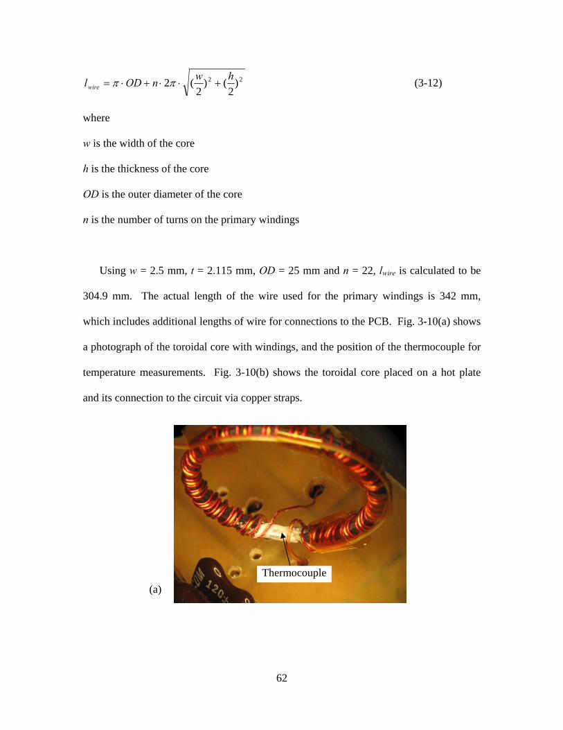
62
22 )2
()2
(2 hwnODlwire +⋅⋅+⋅= ππ (3-12)
where
w is the width of the core
h is the thickness of the core
OD is the outer diameter of the core
n is the number of turns on the primary windings
Using w = 2.5 mm, t = 2.115 mm, OD = 25 mm and n = 22, lwire is calculated to be
304.9 mm. The actual length of the wire used for the primary windings is 342 mm,
which includes additional lengths of wire for connections to the PCB. Fig. 3-10(a) shows
a photograph of the toroidal core with windings, and the position of the thermocouple for
temperature measurements. Fig. 3-10(b) shows the toroidal core placed on a hot plate
and its connection to the circuit via copper straps.
(a)
Thermocouple

63
Table 3-4 tabulates the AC resistance per unit length, Rac/l of the wire for various
frequencies as obtained from Maxwell 2D simulations and the resistance of the primary
windings at various frequencies.
Table 3-4 AC resistance per unit length of AWG 25 wire and resistance of primary
windings at various frequencies.
f [MHz] Rac / l [Ω/m] Rac [mΩ]
1 0.212 72.6
2 0.287 98.3
3 0.345 118.1
4 0.394 134.8
At a maximum AC peak current of 2.12 A, the power loss in the primary windings at
4 MHz is 303 mW, which is far lower than the projected core loss of around 20 W. DC
Figure 3-10. Toroidal core for loss measurement. (a) Position of thermocouple on core, (b) toroidal core connection with circuit via copper straps.
(b)
Copper straps
Toroidal core
Hot plate
Circuit board Thermocouple

64
pre-magnetization is provided by means of a DC winding. Assuming the relative
permeability of the core is 60 and the maximum peak-to-peak flux density, Bm, is 50 mT,
the corresponding maximum magnetic field intensity, HAC, is calculated to be 663 A/m.
In the design of an inductor for VRM applications, the current ripple is designed to be
around 40 % of the DC current as a rule of thumb. Following this rule of thumb, we let
the AC magnetic flux intensity, HAC, to be 40 % that of the DC magnetic flux intensity,
HDC. This gives a value of HDC = 1658 A/m. Due to consideration of the availability of
the magnet wires, the ease of winding the wire around the core, while minimizing the
number of turns of wire wound around the core, magnet wire of AWG 22 is chosen. For
Jmax = 10 A/mm2, the maximum current is Imax = 3.26 A. Using the relation
maxINlH DCmDC ⋅=⋅ , the number of DC turns is calculated to be 36. To give more
headroom, 40 turns are used for the DC winding, and a current of 2.92 A results in a
magnetic flux intensity of 1658 A/m.
3.3.2.3 Resonant Capacitor
The purpose of introducing resonant capacitor is to increase the voltage drop across
the primary windings of the transformer and to provide current to the primary windings.
The capacitance value is chosen such that it resonates with the primary windings and
produces high impedance at the frequency of interest. Table 3-5 shows the types of
capacitors, their corresponding equivalent series inductance (ESL), equivalent series
resistance (ESR) and equivalent parallel resistance (RP). In the choice of the resonant
capacitor, low ESL and ESR are desired. A low ESL will help push the self resonant
frequency to higher frequencies and produce less impact on the parallel resonant peak. A
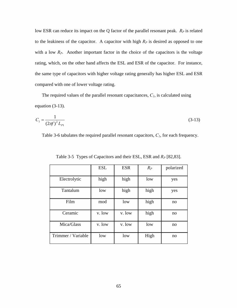
65
low ESR can reduce its impact on the Q factor of the parallel resonant peak. RP is related
to the leakiness of the capacitor. A capacitor with high RP is desired as opposed to one
with a low RP. Another important factor in the choice of the capacitors is the voltage
rating, which, on the other hand affects the ESL and ESR of the capacitor. For instance,
the same type of capacitors with higher voltage rating generally has higher ESL and ESR
compared with one of lower voltage rating.
The required values of the parallel resonant capacitances, C1, is calculated using
equation (3-13).
121 )2(
1
PLfC
π= (3-13)
Table 3-6 tabulates the required parallel resonant capacitors, C1, for each frequency.
Table 3-5 Types of Capacitors and their ESL, ESR and RP [82,83].
ESL ESR RP polarized
Electrolytic high high low yes
Tantalum low high high yes
Film mod low high no
Ceramic v. low v. low high no
Mica/Glass v. low v. low low no
Trimmer / Variable low low High no

66
Table 3-6 Required Parallel Resonant Capacitors, C1, for Each Frequency.
f [MHz] C1 [nF]
1 10.1
2 2.52
3 1.12
4 0.631
5 0.404
3.3.2.4 Current Sense Resistors
In the choice of current viewing resistors, two types of thick film resistors are
compared, which are namely the 2512 and 0603 packages. The resistors for comparison
are 1 Ω resistors. The smaller package resistors have a lower power rating of 0.1 W,
which makes it undesirable since the peak AC current passing through the primary coils
is designed to be 2.12 A, as mentioned in section 3.3.3.2. On the other hand, the 2512
package resistors have a rating of 2 W, which makes it more desirable for this
application. The current sense resistance should not be too large since it is in series with
the primary coils and may decrease the Q factor of the parallel branch of C1 and the
primary coils. Besides, the current sense resistance should not be too small as it may
pose problems in the accurate measurement of voltage across itself. Hence, the resistance
chosen is 0.5 Ω, which is two 1 Ω resistors in parallel. Since the peak current is designed
to be 2.12 A, the maximum power dissipation in the two parallel resistors is 1.12 W each,
which is below the power rating of the resistors. The Q factor is 31, which is still
reasonably large. The minimum current is designed to be 0.212 A. This translates to a

67
voltage of 106 mV to be measured across the current sense resistors, which is sufficiently
large to be measured by the oscilloscope probe.
3.3.2.5 DC Blocking Capacitor
The purpose of the DC blocking capacitor, C2, serves to prevent any DC voltage from
biasing the primary coils. Hence, its AC impedance has to be sufficiently small. For the
DC blocking capacitor, a ceramic capacitor is chosen due to its low ESR and ESL (see
Table 3-5). Although a 100 μF capacitor theoretically yields an impedance of 1.6 mΩ at
1 MHz, however, due to the presence of ESL of the capacitor, the self resonant frequency
occurs below 1 MHz, which results in higher actual impedance observed, as illustrated in
Fig. 3-11. The actual impedance between 1 to 5 MHz lies in the range of 45 to 200 mΩ.
3.3.2.6 AC choke
The purpose of the AC choke, L1, serves to minimize the impact of AC signals on the
DC coils. Hence, its AC impedance has to be sufficiently large. The choke has an
1.E-03
1.E-02
1.E-01
1.E+00
1.E+01
1.E+02
1.E+00 1.E+02 1.E+04 1.E+06 1.E+08 1.E+10
frequency [Hz]
Mag
nitu
de [o
hm]
CeramicElectrolytic
Figure 3-11 Impedance characteristics of a 100 μF ceramic capacitor and a 100 μF electrolytic capacitor.
Impe
danc
e [Ω
]

68
inductance of 162.3 μH. The choke is designed such that its self-resonant frequency is
above our frequency of interest, while ensuring a sufficiently large impedance. Figure 3-
12 shows the magnitude and phase plot of the AC choke measured using an impedance
analyzer. As observed from Fig. 3-12, the self resonant frequency is 5.83 MHz, which is
above the frequency range of interest (1 to 4 MHz). This will ensure inductive behavior
in our frequency range of interest.
Figure 3-12 Impedance characteristics of AC choke (a) Magnitude vs. frequency, (b)phase vs. frequency.
Frequency
Self resonant frequency
69
3.4 Sources of Measurement Error
Accuracy in high frequency electrical characterization of a low loss magnetic material
proves to be a challenge due to the large angle between the voltage and current
waveforms measured. Any displacement of the measured voltage and current waveform
in time can result in large errors in power loss measurement. Two basic types of error are
magnitude error and phase error in the measured waveforms [78]. These errors can be
come from various sources in the measurement circuit. In this section, the various
sources of error will be identified and analyzed.
3.4.1 Error due to Oscilloscope
A. Magnitude Error
The magnitude error from an oscilloscope measurements arises from the vertical
resolution of the oscilloscope. The minimum power loss measurement error due to an
oscilloscope can be expressed as shown in equation (3-14) [84, page 178]. For 8 bits
resolution, the minimum magnitude error is 0.39 % and the minimum power loss error is
0.78 %, assuming the waveform spans the entire oscilloscope screen. If the waveform
spans half the oscilloscope screen, the magnitude error is 0.78 % and the power loss error
is 1.57 %.
Power loss error %100)1
)211(1
,1
1)211(
max(
22
×−−−+
=nn (3-14)
where n is the number of bits

70
Hence, for waveforms spanning between half the screen in the vertical direction to the
entire screen, the magnitude error will be between 0.39 % to 0.78 %. If two probes are
used in the measurement of the power, where the two voltages are multiplied, their errors
add up. The power loss error is between 0.78 % to 1.57 %.
B. Phase Error
The phase error from an oscilloscope measurement results from the sampling rate
used. For a sampling rate of 5 GS/s, the phase error induced is [84]
Phase error 9105360××
=° f (3-15)
For a single probe, for a 1MHz signal the phase error is 0.072° and for a 5 MHz signal,
the phase error is 0.36°.
3.4.2 Errors due to Probe / Cable
A. Magnitude Error
The measurement of voltages across an inductor can result in a magnitude error as a
result of resonance with the input capacitance of the measurement probe or cable.
Capacitive loading of the device under test (DUT) becomes increasingly important as
frequency increases [85]. The problem is aggravated when ringing is introduced into the
circuit when used with long ground leads. This implies the need for careful electrical
grounding. Input capacitance of a 2 feet coaxial cable, Tektronix P5050 [86] and P6243
[87] oscilloscope probes are measured using the Agilent 4294A impedance analyzer with
42941A probe. Figure 3-13 shows the equivalent circuit of voltage measurement across
secondary side of transformer. Fig. 3-14 shows the percentage magnitude error vs.

71
frequency due to parallel resonance between the inductor and input capacitance of probe
with different input capacitances. Table 3-7 tabulates input capacitance, resonant
frequency and magnitude error for measuring voltage across a 3 μH inductor, as an
example, using the 2 feet coaxial cable, P5050 and P6243 oscilloscope probes.
It is clear that at higher frequencies, using a coaxial cable for measuring voltages
across inductors generate large magnitude errors, as a result of large input capacitance.
Although P6243 has the smallest input capacitance, its major limitation is its low input
voltage range of ± 15 V. The P5050 is chosen due to its higher voltage rating of ± 300 V
and wide bandwidth of 500 MHz. Figure 3-15 shows the percentage magnitude error vs.
Figure 3-14. Percentage magnitude error due to resonance between inductance of coil (L = 3 μH) and input capacitance of probe.
2.15 %
8.77 %
0.25 %
4 MHz
% m
agni
tude
err
or
LCin
Probe / Cable
(a)
Figure 3-13. Equivalent circuit of voltage measurement across secondary side of transformer

72
inductance using oscilloscope probe P5050 with input capacitance of 11.1 pF. The
magnitude error at 5 MHz when measuring voltage across an inductance of 3 μH is 3.4%.
Table 3-7 Input capacitance, resonant frequency and magnitude error for measuring
voltage across a 3 μH inductor.
Coax P5050 [86] P6243 [87]
Input capacitance [pF] 42.54 11.1 1.33
Resonant frequency [MHz] 17.3 33.8 97.6
Mag error at 1 MHz [%] 0.51 0.13 0.016
Mag error at 4 MHz [%] 8.77 2.15 0.25
Mag error at 5 MHz [%] 14.4 3.40 0.40
Figure 3-15. Percentage magnitude error vs. inductance using oscilloscope probe P5050 with input capacitance of 11.1 pF.
0 1 2 3 4 50
1
2
3
4
5
6
% m
agni
tude
err
or [%
]
L [uH]
Magnitude error vs. inductance
4 MHz5 MHz
3.4 %
L [μH]

73
B. Phase Error
The bandwidth of the probe can result in a phase error in voltage measurements.
Assuming first order filter characteristics, the phase error for a 500 MHz probe at 1 MHz
is -0.1145° and at 5 MHz is -0.5724°. If the same type of probe is used for measuring
voltage across the secondary coils as well as voltage across the current sense resistors, the
phase error due to bandwidth will cancel out.
Another source of phase error results from the propagation delay of the probe or
cable. When two voltage measurements are taken simultaneously, the propagation delay
is the difference between their propagation delays. However, their tolerances add up.
For instance, if two Tektronix P6243 probes are used, the error due to propagation delay
will be ± 0.4 ns (see Table 3-8). Table 3-8 tabulates the phase error due to propagation
delay for a 2 feet coaxial cable and the Tektronix P5050 and P6243 oscilloscope probes.
Table 3-8 Propagation delay and phase error for a 2 feet coaxial cable and the P6134 and
P6243 oscilloscope probes.
Coax P5050 [86] P6243 [87]
Propagation delay [ns] 2.0 5.5 5.3 ± 0.2
Phase error @ 1MHz 0.72 1.98 1.91
Phase error @ 5MHz 3.6 9.9 9.54
Since P5050 is used and the tolerance is not given in the datasheet, the phase error
due to this tolerance is not considered. Since P5050 probe is used for both measuring

74
voltage across the secondary coils as well as voltage across the current sense resistors, the
propagation delay of 5.5 ns is assumed to cancel out.
3.4.3 Error due to Current Sense Resistor
A. Magnitude Error
The choice of current sense resistors determines the magnitude error it causes. One
source of error is the tolerance of the resistor. For a 1 Ω, 1 % resistor, the error range is
from 0.995 Ω to 1.005 Ω. Another source of magnitude error is due to the equivalent
series inductance (ESL) of the sense resistor. However, since the internal structure of the
resistor is unknown and the ESL is too small to be measured accurately, its impact on the
magnitude error is not considered here. Fig. 3-16 shows the equivalent circuit for voltage
measurement across the current sense resistor.
In summary, the magnitude error due to the current sense resistors is ± 0.5 %.
Figure 3-16. Equivalent circuit of voltage measurement across current sense resistor.
Rsense
Lsense
Cin
Probe I

75
B. Phase Error
Since the internal structure of the resistor is unknown and the ESL of the current
sense resistor is too small to be measured accurately, its impact on the phase error is not
considered here.
3.4.4 Error due to Noise in Measurement
The ground return loop, in addition to resonating with the probe’s input capacitance
and affecting probe rise time, picks up noise from electromagnetic fields from the
environment. The voltage that is induced is proportional to the enclosed loop area [88].
Hence, it is necessary to minimize this loop area. Fig. 3-17 shows the oscilloscope screen
with the noise band and the offset voltage. Since the noise is statistical in nature, the
noise can be eliminated by taking an average. However, the offset voltage has to be
taken into account in the measurements.
3.4.5 Error due to Phase shift between V and I
For a voltage and a current waveform displaced at an angle of θ, the power loss is
given by:
)cos(θVIP = (3-16)
Figure 3-17. Oscilloscope screen with the noise band and the offset voltage.
± 5 mV Vmean
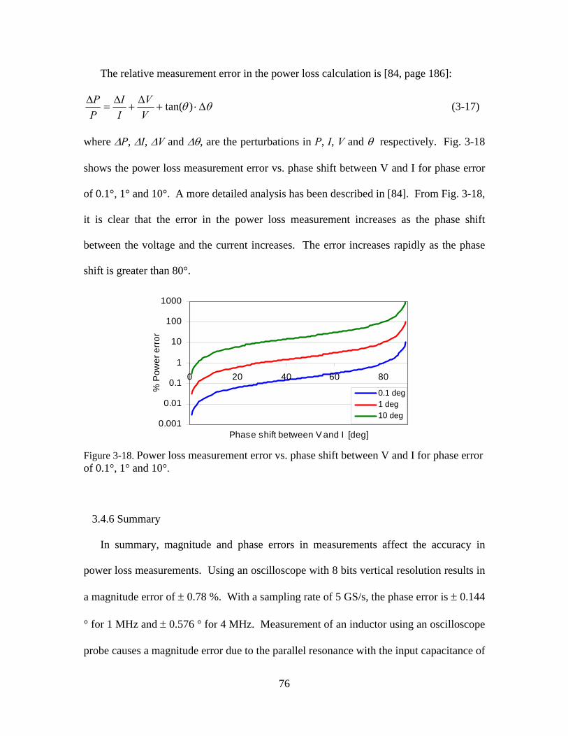
76
The relative measurement error in the power loss calculation is [84, page 186]:
θθ Δ⋅+Δ
+Δ
=Δ )tan(
VV
II
PP (3-17)
where ΔP, ΔI, ΔV and Δθ, are the perturbations in P, I, V and θ respectively. Fig. 3-18
shows the power loss measurement error vs. phase shift between V and I for phase error
of 0.1°, 1° and 10°. A more detailed analysis has been described in [84]. From Fig. 3-18,
it is clear that the error in the power loss measurement increases as the phase shift
between the voltage and the current increases. The error increases rapidly as the phase
shift is greater than 80°.
3.4.6 Summary
In summary, magnitude and phase errors in measurements affect the accuracy in
power loss measurements. Using an oscilloscope with 8 bits vertical resolution results in
a magnitude error of ± 0.78 %. With a sampling rate of 5 GS/s, the phase error is ± 0.144
° for 1 MHz and ± 0.576 ° for 4 MHz. Measurement of an inductor using an oscilloscope
probe causes a magnitude error due to the parallel resonance with the input capacitance of
Figure 3-18. Power loss measurement error vs. phase shift between V and I for phase error of 0.1°, 1° and 10°.
0.001
0.01
0.1
1
10
100
1000
0 20 40 60 80
Phase shift between V and I [deg]
% P
ower
err
or
0.1 deg1 deg10 deg

77
the probe. The bandwidth of the probe can result in a phase error in voltage
measurements. The other source of error results from the propagation delay of the probe
or cable. However, when two probes of the same type are used simultaneously to obtain
voltage waveforms, these two errors in phase cancel out. The choice of current sense
resistors determines the magnitude error it causes. For a resistor with tolerance of 1 %,
the magnitude error in voltage measurement is ± 0.5 %. Noise in voltage measurement is
statistical in nature, which can be eliminated by taking an average. However, the offset
voltage has to be taken into account in the measurements. For instance, the mean of a
complete cycle has to be subtracted from the voltage waveform before using it for loss
calculations. The phase shift between the voltage and current waveforms affects its
susceptibility to small phase errors in measurement. Tables 3-9 and 3-10 summarize the
magnitude and phase errors respectively.
Table 3-9 Summary of Magnitude Error.
Source of error f = 1MHz f = 4 MHz
1. Oscilloscope (resolution = 8 bits) ± 0.78 % ± 0.78 %
2. Probe + 0.13 % + 2.15 %
3. Sense resistors ± 0.5 % ± 0.5 %
4. Measurement noise N/A N/A
Lower bound of magnitude error - 1.28 % -1.28 %
Upper bound of magnitude error 1.41 % 3.43 %
78
Table 3-10 Summary of Phase Error.
Source of error f = 1MHz f = 4 MHz
1. Oscilloscope (5 GS/s) ± 0.144 ° ± 0.576 °
2. Probe N/A N/A
3. Sense resistors N/A N/A
4. Measurement noise N/A N/A
Lower bound of phase error - 0.144 ° - 0.576 °
Upper bound of phase error 0.144 ° 0.576 °
Assume the original voltage and current waveforms are v and i, where i lags v by an
angle φ. v1 and i1 are the voltage and current waveforms with a positive magnitude error
and a phase error which will decrease the phase shift between the voltage and the current,
leading to the maximum positive power error. v2 and i2 are the voltage and current
waveforms with a negative magnitude error and a phase error which will increase the
phase shift between the voltage and the current, leading to the maximum negative power
error. The voltages, currents, power and power error are as defined:
)sin(0 tVv ω= (3-18)
)sin(0 φω −= tIi (3-19)
)sin()1( 01 tVMv u ωΔ+= (3-20)
)sin()1( 01 φφω Δ+−Δ+= tIMi u (3-21)
)sin()1( 02 tVMv l ωΔ−= (3-22)
)sin()1( 02 φφω Δ−−Δ−= tIMi l (3-23)

79
ivp ⋅= (3-24)
111 ivp ⋅= (3-25)
222 ivp ⋅= (3-26)
% maximum positive power error %1001 ×−
=p
pp (3-27)
% maximum negative power error %1002 ×−
=p
pp (3-28)
where
V0 - peak voltage
I0 - peak current
ω - angular frequency
t - time
φ - phase shift between voltage and current
uMΔ - upper bound of magnitude error
lMΔ - lower bound of magnitude error
Δφ - phase error
Figure 3-19 shows the percentage power error vs. phase shift between current through
primary coils and voltage across secondary coils for 1 MHz and 4 MHz signal, using (3-
27) and (3-28), considering total magnitude error and total phase error.

80
3.5 Operational Influence on Electromagnetic Characteristics of LTCC
Magnetic Material
Numerous loss models have been developed to characterize core losses in magnetic
materials. Jiles and Atherton [89], Coleman and Hodgdon [90], and Preisach [91]
developed the static hysteresis models. Subsequently, frequency dependent losses [92-
97] has been included into the above static models. The most common and widely used
method is the Steinmetz equation [79], which relates volumetric power loss to magnetic
flux density and frequency. The Steinmetz equation has been subsequently modified to
include losses due to DC premagnetization [98], influence of non-sinusoidal waveforms
[73, 99] and remagnetization [100] and temperature [79].
84 85 86 87 88 89 90-80
-60
-40
-20
0
20
40
60
80
phase shift [deg]
% p
ower
err
or
Figure 3-19. Percentage power error vs. phase shift between current through primary coils and voltage across secondary coils for 1 MHz and 4 MHz, considering total magnitude error and total phase error.
1 MHz
1 MHz
4 MHz
4 MHz

81
In this dissertation, Steinmetz equation with temperature dependence [79] is used to
model core loss. The temperature coefficients include magnetic flux density dependence
with temperature and temperature dependence of the Steinmetz exponents. Effect of DC
pre-magnetization on these coefficients and exponents is also studied.
3.5.1 Effect of Frequency on Electromagnetic Characteristics
The basic Steinmetz equation is given by:
βα BfKP pv ⋅⋅= (3-29)
In this set of measurements, frequency is varied and the Steinmetz exponents are
obtained for each frequency. Fig. 3-20 shows the specific power loss vs. peak-to-peak
flux density for frequencies between 1 to 5 MHz. From Fig. 3-20, the gradient of the
curves yields β and the vertical intercept yields )log( αfK p ⋅ . The average β for 1 MHz
to 5 MHz is 2.06. Fig. 3-21 shows the plot of )log( αfK p ⋅ vs. log (f). From Fig. 3-21,
α is estimated to be 1.255 and Kp is 1.32 x 10⁻⁵.
Hence for T = 26 °C and IDC = 0 A, the volumetric power loss can be expressed as:
06.2255.151032.1 BfPv ⋅⋅×= − .

82
3.5.2 Effect of Pre-magnetization on Electromagnetic Characteristics
The loss measurement described above is repeated for frequencies between 1 MHz to
4 MHz with application of a DC current of IDC = 0.67 A, 1.1 A, 2.2 A and 3.1 A. Fig. 3-
22 shows the change of β with IDC. Fig. 3-23 shows the curves of )log( αfK p ⋅ vs. log(f)
for IDC between 0 A to 3 A. The gradient of the curves yields α and the vertical intercept
Figure 3-20 Specific power loss vs. peak-to-peak flux density for frequencies between 1 to 5 MHz at T = 26 °C and IDC = 0 A.
-3.0
-2.5
-2.0
-1.5
-1.0
-0.5
0.0
0.5
1.0
1.5
-3 -2.5 -2 -1.5 -1
log(B)
log(
Pv)
1MHz2MHz3MHz4MHz5MHz
Figure 3-21 Graph of log(Kp*f α) vs. log (f) at T = 26 °C and IDC = 0 A.
y = 1.255x - 4.8783
2
2.5
3
3.5
4
5.8 6 6.2 6.4 6.6 6.8log(f)
log(
K p·fα
) log(Kp*f α)=1.255log (f) -4.8783

83
yields log (Kp). Fig. 3-24 shows the plot of α vs. IDC at T = 26 °C and Fig. 3-25 shows
the plot of Kp vs. IDC at T = 26 °C. From Fig. 3-22, Fig. 3-24 and Fig. 3-25, α, β and Kp
can be expressed as a function of IDC in the form of:
21)( aIaI DCDC +⋅=α (3-30)
21)( bIbI DCDC +⋅=β (3-31)
)exp()( 21 DCDCp IkkIK ⋅⋅= (3-32)
Figure 3-23 Graph of )log( αfK p ⋅ vs. IDC at T = 26 °C.
2.5
3
3.5
4
4.5
5.8 6 6.2 6.4 6.6 6.8log(f)
IDC = 0 AIDC = 0.67 AIDC = 1 AIDC = 2 AIDC = 3 A
log(
Kp·fα
)
Figure 3-22 Graph of β vs. IDC at T = 26 °C.
y = -0.0181x + 2.0698
1.98
2
2.02
2.04
2.06
2.08
2.1
0 1 2 3 4I DC [A]
β
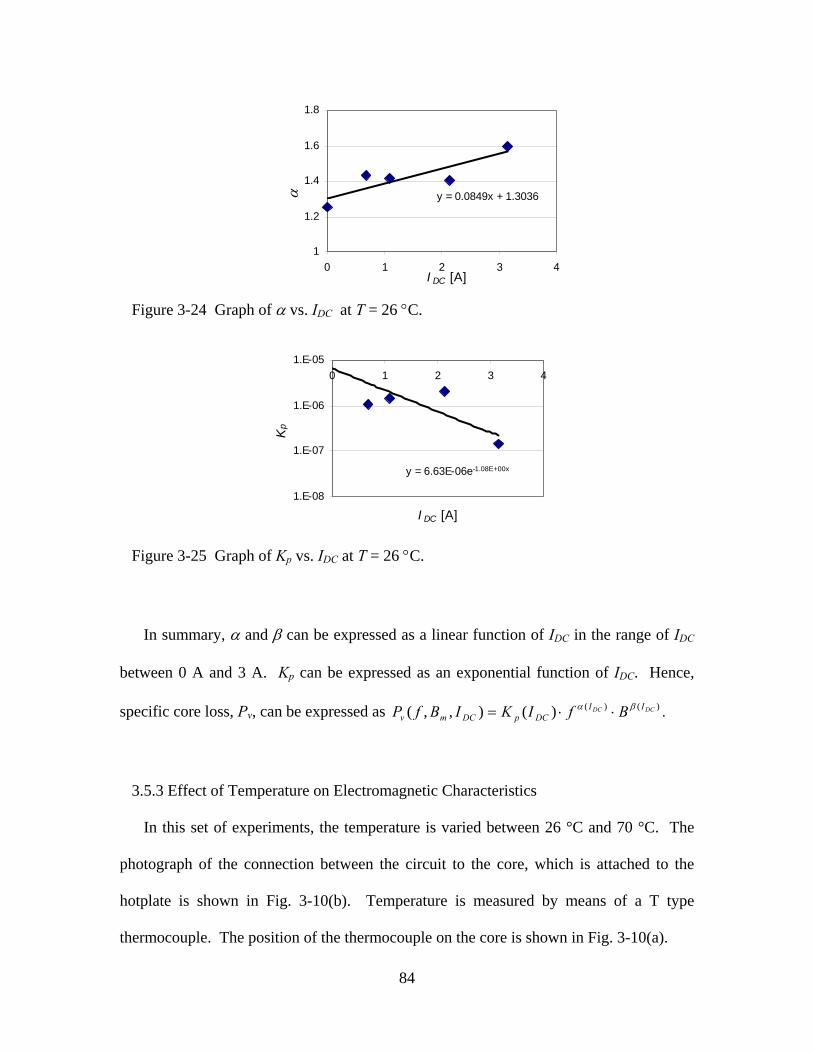
84
In summary, α and β can be expressed as a linear function of IDC in the range of IDC
between 0 A and 3 A. Kp can be expressed as an exponential function of IDC. Hence,
specific core loss, Pv, can be expressed as )()()(),,( DCDC IIDCpDCmv BfIKIBfP βα ⋅⋅= .
3.5.3 Effect of Temperature on Electromagnetic Characteristics
In this set of experiments, the temperature is varied between 26 °C and 70 °C. The
photograph of the connection between the circuit to the core, which is attached to the
hotplate is shown in Fig. 3-10(b). Temperature is measured by means of a T type
thermocouple. The position of the thermocouple on the core is shown in Fig. 3-10(a).
y = 6.63E-06e-1.08E+00x
1.E-08
1.E-07
1.E-06
1.E-050 1 2 3 4
I DC [A]
Kp
Figure 3-25 Graph of Kp vs. IDC at T = 26 °C.
y = 0.0849x + 1.3036
1
1.2
1.4
1.6
1.8
0 1 2 3 4I DC [A]
αFigure 3-24 Graph of α vs. IDC at T = 26 °C.

85
In the development of the core loss model, Steinmetz equation [79] is used. Equation
(3-33) shows the Steinmetz equation taking into account temperature dependence [79].
)(' 12
2 tttv cTcTcBfkP ++⋅⋅⋅= βα (3-33)
In addition to the temperature dependence on losses, temperature dependence of
Steinmetz exponents is also taken into account. Fig. 3-26 shows the graphs of (a) α vs.
IDC, (b) β vs. IDC and (c) Kp vs. IDC. for T = 26, 50 and 70 °C. α varies within ± 17.5 % of
its mean value and β varies between ± 5 % of its mean value. Fig. 3-27 shows the graphs
of the coefficients a1, a2, b1, b2, k1, and k2 (as defined in (3-30) to (3-32)) vs. temperature,
T, which are fitted using second order polynomial.
1.9
2
2.1
2.2
2.3
0 500 1000 1500 2000HDC [A/m]
β
26 C50 C70 C
(b)
26 °C 50 °C 70 °C
1
1.2
1.4
1.6
1.8
0 500 1000 1500 2000HDC [A/m]
α
26 C50 C70 C
(a)
26 °C 50 °C 70 °C
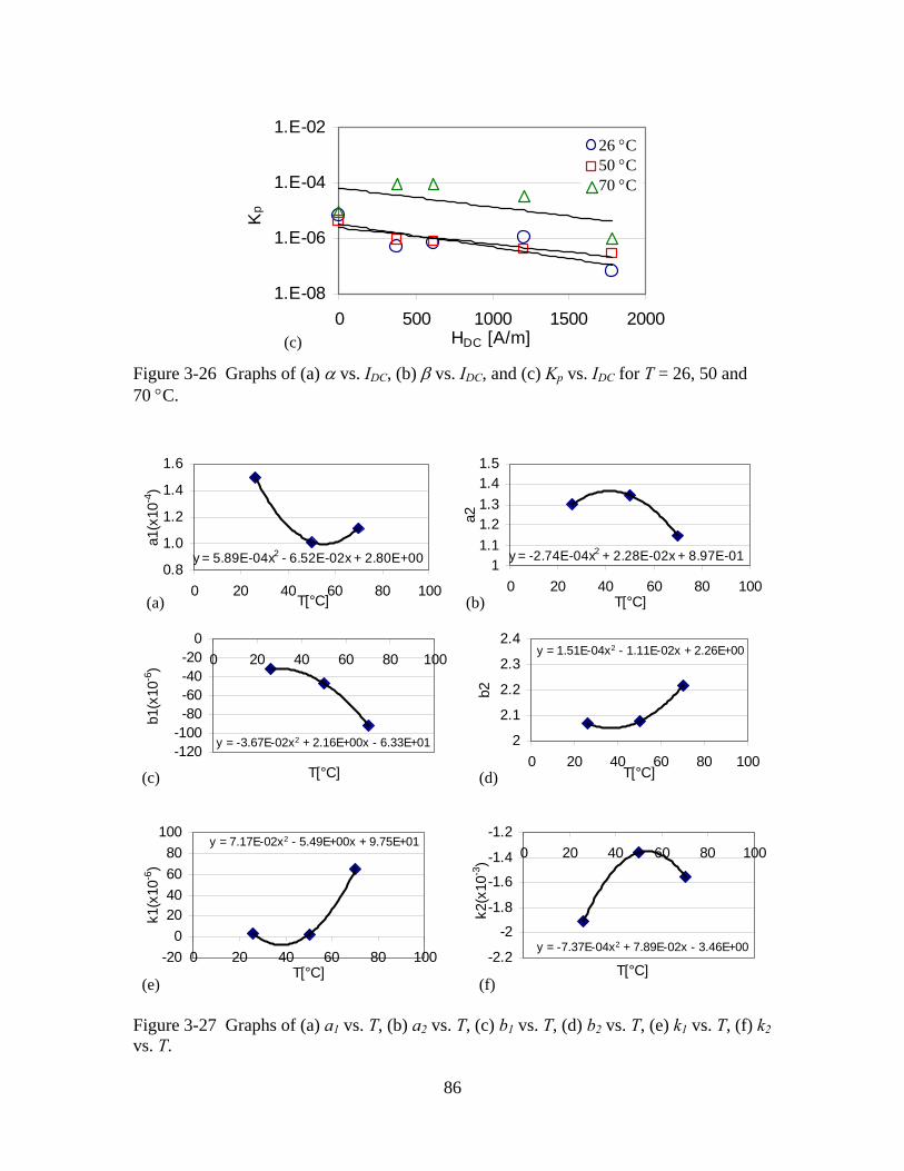
86
1.E-08
1.E-06
1.E-04
1.E-02
0 500 1000 1500 2000HDC [A/m]
Kp
26 C50 C70 C
Figure 3-26 Graphs of (a) α vs. IDC, (b) β vs. IDC, and (c) Kp vs. IDC for T = 26, 50 and 70 °C.
26 °C 50 °C 70 °C
(c)
y = -7.37E-04x2 + 7.89E-02x - 3.46E+00-2.2
-2
-1.8
-1.6
-1.4
-1.20 20 40 60 80 100
T[°C]
k2(x
10-3
)
y = 7.17E-02x2 - 5.49E+00x + 9.75E+01
-200
20406080
100
0 20 40 60 80 100T[°C]
k1(x
10-6
)
Figure 3-27 Graphs of (a) a1 vs. T, (b) a2 vs. T, (c) b1 vs. T, (d) b2 vs. T, (e) k1 vs. T, (f) k2vs. T.
(e) (f)
y = -3.67E-02x2 + 2.16E+00x - 6.33E+01-120-100-80-60-40-20
00 20 40 60 80 100
T[°C]
b1(x
10-6
)
y = 1.51E-04x2 - 1.11E-02x + 2.26E+00
2
2.1
2.2
2.3
2.4
0 20 40 60 80 100T[°C]
b2
(c) (d)
y = 5.89E-04x2 - 6.52E-02x + 2.80E+000.8
1.0
1.2
1.4
1.6
0 20 40 60 80 100T[°C]
a1(x
10-4
)
y = -2.74E-04x2 + 2.28E-02x + 8.97E-011
1.11.21.31.41.5
0 20 40 60 80 100T[°C]
a2
(a) (b)

87
The specific core loss can be expressed as:
),(),(),(),,,( TITIDCpDCmv
DCDC BfTIKTIBfP βα ⋅⋅= (3-34)
where
)()(),( 21 TaITaTI DCDC +⋅=α (3-35a)
)()(),( 21 TbITbTI DCDC +⋅=β (3-35b)
))(exp()(),( 21 DCDCp ITkTkTIK ⋅⋅= (3-35c)
16.01076.31041.3)( 3251 +⋅×−⋅×= −− TTTa (3-35d)
898.01027.21074.2)( 2242 +⋅×+⋅×−= −− TTTa (3-35e)
036.01023.11008.2)( 3251 −⋅×+⋅×−= −− TTTb (3-35f)
26.21011.11051.1)( 2242 +⋅×−⋅×= −− TTTb (3-35g)
45271 1095.1101.11043.1)( −−− ×−⋅×−⋅×= TTTk (3-35h)
95.11041.41011.4)( 2242 −⋅×+⋅×−= −− TTTk (3-35i)
The empirical model described by the equation (3-34) and (3-35) is based on the
toroidal core of a certain size with a certain number of turns of windings. To use it to
estimate core loss for a magnetic component of different dimensions and number of turns
of windings, expressing the model as a function of magnetic field intensity would be
more appropriate.
The specific core loss can be expressed as:
),,(),,(),,(),,,( nTHnTHDCpDCmv
DCDC BfnTHKTHBfP βα ⋅⋅= (3-36)
where
)()(),,,( 21 TaHTanlTH DCmDC +⋅=α (3-37a)
)()(),,,( 21 TbHTbnlTH DCmDC +⋅=β (3-37b)
88
))(exp()(),,,( 21 DCmDCp HTkTknlTHK ⋅⋅= (3-37c)
46281 108.21052.61089.5)( −−− ×+⋅×−⋅×= TTTa (3-37d)
897.01028.21074.2)( 2242 +⋅×+⋅×−= −− TTTa (3-37e)
56281 1033.61016.21067.3)( −−− ×−⋅×+⋅×−= TTTb (3-37f)
26.21011.11051.1)( 2242 +⋅×−⋅×= −− TTTb (3-37g)
56281 1075.91049.51017.7)( −−− ×−⋅×−⋅×= TTTk (3-37h)
35272 1046.31089.71037.7)( −−− ×−⋅×+⋅×−= TTTk (3-37i)
Hence, due to the effect of DC pre-magnetization, an additional exponential term is
added to (3-36). The specific core loss taking into account effects of IDC and temperature
can be expressed as:
))(exp()(),,,( 212
2),,(),,(
DCtttnTH
mnTH
DCmv HTkcTcTcBfTHBfP DCDC ⋅⋅+⋅+⋅⋅⋅= βα
(3-38)
where ct2, ct1, and ct, are the coefficients of k2(T).
3.5.4 Model comparison with actual data
The model developed in this section is obtained by empirical means. The accuracy of
the model depends on how well the equations describe the data. The discrepancy
between the fitted curve and the data plotted on a log scale is usually magnified when
plotted on a linear scale. Fig. 3-28 shows the plot of Fig. 3-20 plotted on linear scale,
where the dots represent experimental data and the lines are the fitted curves. Figure 3-
29 shows the percentage error between the fitted curves and the experimental data vs.
magnetic flux density. It is clear from this plot that the error between the basic Steinmetz

89
model and the experimental data can be as large as several tens of percent. The
percentage error between the model and the experimental data is given as:
%100(exp)
(mod)(exp)% ×
−=
v
vv
PPP
error (3-39)
Figure 3-30 shows the percentage error between experimental data and model vs. Bm
for (a) 1 MHz, (b) 2 MHz, (c) 3 MHz and (d) 4 MHz, at 26 °C, 50 °C, 70 °C and IDC = 0
Figure 3-29 Percentage error between fitted curves and experimental data, for frequencies between 1 to 5 MHz at T = 26 °C and IDC = 0 A.
-30
-20
-10
0
10
20
30
0 10 20 30 40 50 60
B [mT]
% e
rror
1M Hz2M Hz3M Hz4M Hz5M Hz
0
1
2
3
4
5
6
0 10 20 30 40 50 60B [mT]
P v [W
/cc]
1MHz2MHz3MHz4MHz5MHz
Figure 3-28 Specific power loss vs. peak-to-peak flux density and or frequencies between 1 to 5 MHz at T = 26 °C and IDC = 0 A.

90
A and 3 A. The error range is between -65 % to 33 %, which is due to discrepancy
between experimental data and fitted curve. Fig. 3-31 is the same as Fig. 3-19, indicating
the range of phase shifts between voltage and current waveforms measured at 1 MHz and
4 MHz. The range of phase shift for each frequency is obtained from the experimental
voltage and current waveforms to obtain a peak-to-peak flux density in the range of 5 mT
to 50 mT, DC magnetic field intensity between 0 A/m to 1780 A/m at a temperature
range of 26 °C to 70 °C. The range of phase shift for 1 MHz is 87.8° to 89.2°. The range
of phase shift for 4 MHz is 87° to 88°.
f=3MHz
-100
-50
0
50
100
1 10 100
B [mT]
%er
ror
f=4MHz
-100
-50
0
50
100
1 10 100
B [mT]
%er
ror
Figure 3-30 Percentage error between experimental data and model vs. peak-to-peakflux density for (a) 1 MHz, (b) 2 MHz, (c) 3 MHz and (d) 4 MHz, at 26 °C, 50 °C, 70 °C and IDC = 0 A and 3 A.
(c) (d)
f=1MHz
-100
-50
0
50
100
1 10 100
B [mT]
%er
ror
f=2MHz
-100
-50
0
50
100
1 10 100
B [mT]
%er
ror
(a) (b)

91
The maximum measurement error range is -21.3 % to +20.1 % for 1 MHz and -37.8
% to +30.6 % for 4 MHz in their respective range of phase shift as indicated in Fig. 3-31.
Since Fig. 3-30 shows the error without considering the error involved in measurement,
when measurement error is included, the total error will be increased by their respective
amounts for 1 MHz and 4 MHz. Figure 3-32 shows the percentage power error vs. peak-
to-peak flux density for (a) f = 1 MHz and (b) f = 4 MHz, considering measurement error
discussed in section 3.4. The maximum measurement error range of -21.3 % to +20.1 %
for 1 MHz is added to every data point in Fig. 3-30(a) to obtain Fig. 3-32(a). The
maximum measurement error range of -37.8 % to +30.6 % for 4 MHz is added to every
data point in Fig. 3-30(d) to obtain Fig. 3-32(b). Hence, the maximum error range of the
model in predicting core loss is between -85.9 % to 63.7 % for a peak-to-peak flux
density in the range of 5 mT to 50 mT, DC magnetic field intensity between 0 A/m to
84 85 86 87 88 89 90-80
-60
-40
-20
0
20
40
60
80
phase shift [deg]
% p
ower
err
or
Figure 3-31 Percentage power error vs. phase shift between current through primarycoils and voltage across secondary coils for 1 MHz and 4 MHz, considering total magnitude error and total phase error. Range of phase shift for 1 MHz and 4 MHz are indicated.
4 MHz
Range of phase shift for 1 MHz
Range of phase shift for 4 MHz
4 MHz
1 MHz
1 MHz
30.6 %
-37.8 %
20.1 %
-21.3 %

92
1780 A/m at a temperature range of 26 °C to 70 °C, inclusive of the possible errors from
measurement.
If temperature and IDC dependence on the Steinmetz exponents, α and β, are not
considered, the ratio of the estimated power using a constant Steinmetz exponent to
actual power due to α or β alone can be expressed as:
),(
)(
)( TI
mean
DCffratio α
α
α = (3-40)
%100)( ),(
)(
×= TIm
meanm
DCBB
ratio β
β
β (3-41)
For ± 17.5 % error in α, ratio(α) ranges between 0.0266 and 37.6, which implies that
the power loss estimated using a constant α can be 37.6 times larger or smaller than the
actual power loss. For a ± 5 % error in β, ratio(β) ranges between 0.577 and 1.733. If
both α or β are considered, the power loss estimated using a constant α and β can be 65
times larger or smaller than the actual power loss. This clearly shows the necessity to
express the Steinmetz exponents as a function of temperature and IDC as opposed to
assuming them as constants.
f=4MHz
-100
-50
0
50
100
1 10 100
B [mT]
%er
ror
f=1MHz
-100
-50
0
50
100
1 10 100
B [mT]
%er
ror
Figure 3-32 Percentage power error vs. peak-to-peak flux density, B for (a) f = 1 MHz and (b) f = 4 MHz, considering measurement error discussed in section 3.4.
(a) (b)
35.8 %
-85.9 %
63.7 %
-55.9 %
93
In summary, core loss is modeled using Steinmetz equation for frequencies between 1
to 4 MHz, peak-to-peak flux density between 5 mT to 50 mT and magnetic flux intensity,
H, between 0 A/m to 1780 A/m. Temperature and DC current dependence are included
in the model to describe their impact on core loss. The error range between the model
and experimental result is between -85.9 % to 63.7 %.
3.6 Electrical Characterization of Conductive Paste
Series resistance of the inductor is an important parameter in power inductor design.
In our fabrication process, we will be using a commercial Ag/Pt paste, also purchased
from Electroscience Labs [28], to form printed conductors. To measure the resistivity of
the Ag/Pt conductors, meander patterns are being screen-printed on 625μm thick alumina
substrates and subsequently sintered using the sintering profile shown in Fig. 3-33. Fig.
3-34(a) shows the meander shaped conductor paste, screen printed on the alumina
substrate. Fig. 3-34(b) shows the magnified cross-sectional view of the conductor
patterns. The series DC resistance of the meander structure is measured and the
resistance measurement results are summarized in Table 3-11.
The average estimated width of the Ag paste is 560μm and the estimated thickness is
62μm. Two approximation methods are used to estimate the cross-sectional area of the
screen-printed conductor paste after sintering. The first method is to use a triangle to
approximate the cross-sectional shape of the printed conductor and the second method is
to approximate it as a segment of a circle as illustrated in Fig. 3-35. Using the equation:
)(1
lRA
=σ (3-42)

94
where
A : cross-sectional area of the conductor
R : resistance of conductor
l : length of conductor
the conductivity of the screen-printed Ag paste can be calculated. Table 3-12 summarises
the results obtained.
Figure 3-34 Cross-sectional view of the inductors (a) L1 and (b) L2.
(a)
(b)
62 μm
560 μm
Printed conductor
Ceramic substrate
Figure 3-33 Sintering profile for Ag/Pt paste.
885°C
450°C
R1=2.0ºC/min
2 hr 4 hrs Natural cooling (~ 6 hrs to 100 °C)
R2=6.0ºC/min T [°C]

95
Table 3-11 Resistance Measurement Of Screen-Printed Conductors
Substrate alumina
Line width [mm] 0.6
Length [mm] 500
R [Ω] 1.42
R/l [Ω/m] 2.84
R/sq [mΩ/sq] 1.704
Table 3-12 Estimated Conductivity Of The Screen-Printed Conductor Paste Using The
Two Methods.
Area [mm2] σ [S/m]
Triangle 1.74×10⁻² 2.02×10⁷
Segment of circle 2.35×10⁻² 1.50×10⁷
As an average, the conductivity, σ, of the post sintered conductor paste is
approximated to be σ = 1.7 x 10⁷ S/m. From here on, we use this value for our
subsequent calculations.
Figure 3-35 Cross-sectional area approximation of screen-printed Ag/Pt conductor using (a) segment of a circle and (b) triangle.
62 μm
560 μm
62 μm
560 μm
(a)
(b)

96
3.7 Summary
In this chapter, characterization of the materials involved in magnetic integration
using LTCC technology has been performed. The permittivity of the LTCC ferrite tape is
estimated to be 13. In core loss measurement, sources of the various errors in the core
loss measurement circuit have been identified, analyzed and quantified. The choice of
the components for the core loss measurement circuit has been discussed and the design
of the core and the windings has been formulated. Finally, the operational influence on
electromagnetic characteristics of LTCC magnetic material is studied and a model based
on Steinmetz equation with temperature and DC current dependence is developed. Core
loss is modeled using Steinmetz equation for frequency between 1 to 4 MHz, peak-to-
peak flux density between 5 mT to 50 mT and magnetic flux intensity, H, between 0 A/m
to 1780 A/m. Temperature and DC current dependence are included in the model to
describe their impact on core loss. The error range between the model and experimental
result is between -85.9 % to 63.7 %.

97
Chapter 4. LTCC Chip Inductor Development
4.1 Overview
This chapter will discuss about the LTCC chip inductor development. The chapter
will start with a comparison of the various inductor geometries found in literature,
followed by geometry selection for high current application. The inductance change with
DC current application for the chosen geometry and the impact of varying inductance on
circuit performance are then discussed. The impact of conductor cross-sectional shape
for the chosen geometry will be discussed and the desired conductor cross-sectional
shape for high current and high frequency application will be selected. The power
inductor fabrication procedure to obtain the desired geometry will be elaborated. Based
on the selected geometry and fabrication procedure, parametric variation of the inductor’s
physical geometry is performed and an empirical inductance model is developed. The
chapter will be concluded by an inductor design procedure.
4.2 Geometry Selection for Integratable Chip Inductor
4.2.1 Comparison of Various Geometries of Planar Inductor
The integrated inductors can take various forms and geometries. This section will
compare the various geometries found in literature and the most suitable geometry will be
selected for our application.

98
4.2.1.1 Toroidal coil inductor
A toroidal coil [21, 101, 102] is a common geometry for an inductor by virtue of its
symmetry. In a toroidal coil inductor, the conductors wrap around the magnetic material,
which is embedded in the substrate. In this geometry, via formation is necessary for an
integrated inductor to connect the conductors above and below the magnetic material.
The inductance can be controlled by the number of turns and the permeability of the
magnetic core selected. This geometry can be chosen if the electrodes have to be close to
each other. By virtue of the resultant higher resistance due to the length of conductor
which wrap around the magnetic core, this geometry may not be the best option for high
current application. Fig. 4-1 shows some toroidal coil inductors on LTCC NiCuZn ferrite
substrate [21].
4.2.1.2 Solenoid inductor
The solenoid inductor [31, 32, 103, 104] is another common geometry. The solenoid
inductor comprises windings wrapped around a magnetic core. The windings form the
Figure 4-1 Toroidal coils on LTCC NiCuZn ferrite substrate [21].
Conductor patterns LTCC ferrite substrate

99
top and bottom layers and the magnetic material is sandwiched between the windings.
Similar to the toroidal coil geometry, via formation is necessary for an integrated inductor
to connect the conductors above and below the magnetic material. A serious
disadvantage of this type of inductor is that the magnetic circuit does not close through
the magnetic material, leading to inefficient use of material and other disadvantages that
confine this to low power applications. This geometry can be selected if the electrodes
are far from each other. Fig. 4-2 show some solenoid micro-transformers and micro-
inductors found in [31, 32, 103, 104].
4.2.1.3 Racetrack or spiral inductor
As opposed to the toroidal coil or solenoid inductor, which the windings wrap around
the core, the racetrack [29, 105] and spiral [106-110] inductor has the core wrapped
around the winding. Here, the magnetic circuit closes through the magnetic core, leading
to much better use of material. For the pot-core structure, the inductor winding is
relatively long. It is suitable for making inductors with high inductance, however, it is
also not the best option for high current applications. Fig. 4-3 shows an on-chip racetrack
winding inductor using NiFe magnetic core [105]. Fig. 4-4 shows an air-core vertical
stacked spiral inductor for RFIC applications [106].
Figure 4-2 Planar inductor with micromachined NiFe magnetic bar [104].
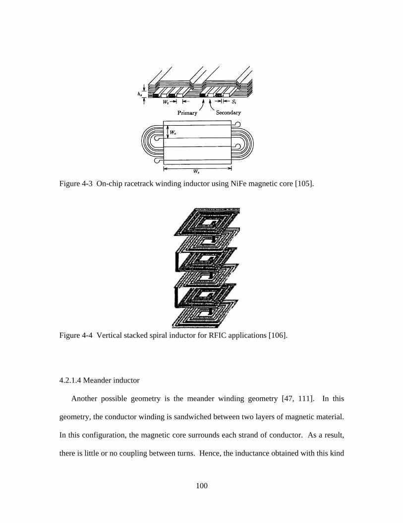
100
4.2.1.4 Meander inductor
Another possible geometry is the meander winding geometry [47, 111]. In this
geometry, the conductor winding is sandwiched between two layers of magnetic material.
In this configuration, the magnetic core surrounds each strand of conductor. As a result,
there is little or no coupling between turns. Hence, the inductance obtained with this kind
Figure 4-4 Vertical stacked spiral inductor for RFIC applications [106].
Figure 4-3 On-chip racetrack winding inductor using NiFe magnetic core [105].

101
of structure does not depend on winding arrangement but rather on its length. Fig. 4-5
shows a thick film meander inductor [47]. The length of the winding will again
contribute appreciably to the conductive losses, making this less suitable for high current
applications.
4.2.1.5 Short winding inductor
The short winding inductor typically comprises a single winding with substantially
large cross-sectional area, with the magnetic core wrapped around it. This kind of
geometry is the most suitable for high current applications. However, the inductance
achievable may be low. The inductance of this type of inductor is determined by the
length of the conductor and the properties of the magnetic material wrapped around it.
Fig. 4-6 shows a V-groove inductor embedded in the silicon [112]. Figure 4-7 shows the
cross-sectional diagram of a thick film planar inductor [47].
Figure 4-5 Thick film meander inductor [47].

102
4.2.1.6 Summary
Based on the above inductor geometries, the short winding inductor with magnetic
core wrapping the conductor gives the flexibility in varying the conductor’s cross-
sectional area. Hence, it is a suitable candidate for achieving low DC resistance and high
current capability.
4.2.2 Concept of Varying Inductance with Bias for Chosen Geometry
By virtue of the absence of a discrete air-gap for the inductor shown in Fig. 4-6 and
Fig. 4-7, any change in the relative permeability of the magnetic core as a result of pre-
Figure 4-7 Cross-sectional diagram of thick film planar inductor [47].
conductor
g
g
e
w
core
Figure 4-6 V-groove inductor embedded in silicon [112].

103
magnetization can result in a change in inductance as illustrated in Fig. 4-8. L2 is a non-
linear inductor and L1 is a linear inductor. This is an effect that relates to both the relative
permeability and the average magnetic path length and will be discussed later in this
chapter.
4.2.3 Impact of Varying Inductance on Circuit Performance
The light load efficiency of a converter is an important factor in extending battery
life. Sun et al. [113] used a non-linear inductor to improve the DCM efficiency for laptop
CPU voltage regulator. A saturable E-I core with stepped center leg is used to realize the
non-linear inductor. The non-linear inductor has a large inductance at CPU sleep state
(light load) and has a small inductance at CPU active state (heavy load).
Using a synchronous buck converter as an example, the impact of varying filter
inductance on circuit performance will be discussed. Fig. 4-9 shows the circuit diagram
of a buck converter. With a larger inductance at light load, the inductor current ripple
will be smaller at a low DC current. With a smaller ripple current, the RMS current
L
IDC
Figure 4-8 Illustration of changing inductance with DC current for non-linear inductor L2 in comparison with a linear inductor L1 with constant inductance with DC current.
IHL
L1
L2
ILL

104
through the switches will be decreased, which can help decrease losses in the switches.
Fig. 4-10 shows the inductor current ripple at heavy load (Δi2) and at light load (Δi1) as a
result of the presence of a non-linear filter inductor. With a smaller inductor current
ripple, the RMS current through the top switch, Itop, as in Fig. 4-9, will be decreased. Fig.
4-11(a) shows the current waveform of the top switch if a small filter inductance is used.
Fig. 4-11(b) shows that when a large filter inductance is used. The switch current
waveform can be described by the following equation (4-1) [114].
2, )(
311
IiDII rmstop
Δ+= (4-1)
Figure 4-9 Buck converter circuit diagram.
25nH
Vo -
+ L
C
Q1
Q2 IL
Io
R Vin
+ VL - Vsw
Itop
IL
t
Figure 4-10 Inductor current when inductance is higher at light load and lower at heavy load.
2Δi1
2Δi2I2
I1

105
It is clear that when the ripple current Δi is small, the RMS current of the switch will
decrease. This helps to decrease losses in the switches, particularly at light load. Figure
4-12 shows the comparison of power stage efficiency, η, vs. DC current for linear
inductor L1 and non-linear inductor L2. When the non-linear inductor, L2, is used, the
light load efficiency will become higher.
η
IDC
Figure 4-12 Power stage efficiency, η, vs. DC current for linear inductor L1 and non-linear inductor L2.
L1
L2
IL
t
Δi2
Δi1
t IL
Itop,2
Itop,1
Figure 4-11 Current waveform of the top switch for (a) small filter inductance and (b) large filter inductance.

106
4.3 Conductor Cross-Sectional Shape Study for Chosen Geometry
The conventional way [115, 116] of screen-printing conductor paste on LTCC tapes
yield elongated conductors with sharp edges. This is by virtue of the way the conductor
paste is printed, and is related to the physics of viscous fluids printed on a surface [117,
118]. Due to electromagnetic considerations, this is found to be detrimental from the
power loss point of view, especially at high operating frequencies.
As discussed in chapter 2, however, the process for manufacturing the inductors can
be modified to have alternative shapes, so that the implications of these different shapes
have to be studied. In this section, the effect of an elongated conductor cross-sectional
shape is evaluated. Different conductor cross-sectional shapes are studied and
comparison are made in terms of power loss in the presence of magnetic material around
the conductor. An experimental verification is made by comparing the performance of
two types of filter inductors, one with elongated cross-sectional shape fabricated using
the conventional conductor screen printing method and the second one is a conductor
with rectangular cross-sectional shape, fabricated using a modified method (refer Chapter
2), that gives a cross-sectional shape close to the desired capsule shape, in a prototype 5V
– to – 1 V Buck converter. A comparison in system performance is made.
4.3.1 Simulation of Conductors with Various Cross-Sectional Shapes
In order to maintain the low profile of embedded passives fabricated using LTCC
technology, alternative conductor shapes chosen for comparison are the rectangular and
the capsule shaped conductor cross-sectional shapes, rather than squares and circles.

107
Figure 4-13 shows the dimensions of the shapes being compared. The cross-sectional
areas of the shapes are kept constant at 0.1 mm2. Conductors with diamond-shaped
cross-section are simulated in place of the almond-shaped conductors, which are typically
formed by screen printing, as shown in Fig. 2-19.
Simulation is performed using Ansoft Maxwell 2D. The conductor’s conductivity
used in the simulation is 1.7x10⁷ S/m, which is an experimentally determined value from
sintered Ag/Pt paste on alumina substrates, as discussed in Chapter 3 of this dissertation.
Simulation is performed for a conductor surrounded by air and a conductor surrounded
by magnetic material of relative permeability 60 and dielectric constant of 13. A
magnetic material of this relative permeability is preferably used for applications where
the frequency exceeds 1 MHz, due to its more favorable characteristics in the frequency
range, as compared to LTCC materials with a higher relative permeability.
4.3.1.1 Conductors in Air
Simulation is performed for conductors with capsule, rectangular and diamond cross-
sectional shapes. Fig. 4-14 shows the 2-D current density distribution for the three types
of conductor cross-sectional shapes. The simulation frequency is 4 MHz and the current
has an amplitude of 1 A.
Figure 4-13 Comparison of conductor cross-sectional shapes, (a) diamond, (b) capsule, and (c) rectangular, for a cross-sectional area of 0.1 mm2.
1 mm
0.2 mm
0.543 mm 0.5 mm
(a) (b) (c)
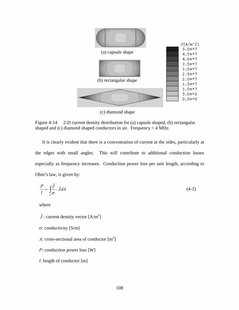
108
It is clearly evident that there is a concentration of current at the sides, particularly at
the edges with small angles. This will contribute to additional conduction losses
especially as frequency increases. Conduction power loss per unit length, according to
Ohm’s law, is given by:
dAJJlP
A∫ ⋅=
rr
σ
where
Jr
: current density vector [A/m2]
σ: conductivity [S/m]
A: cross-sectional area of conductor [m2]
P: conduction power loss [W]
l: length of conductor [m]
(a) capsule shape
(b) rectangular shape
(c) diamond shape
Figure 4-14 2-D current density distribution for (a) capsule shaped, (b) rectangular shaped and (c) diamond shaped conductors in air. Frequency = 4 MHz.
(4-2)

109
To compare the difference in the current density level, the current density is plotted
along the dotted line across the capsule and diamond shaped conductors (see Fig. 4-15),
as the maximum current density for both structures lie along this line. Fig. 4-15 shows
the 1-D current density plot along the red dotted line for the capsule and the diamond
shaped conductors in air. The current density at the sharp corners of the diamond shaped
conductor is approximately double that of the capsule shaped conductor. Fig. 4-16 shows
the comparison of the power loss in the conductors as a function of frequency. The
conductor with diamond cross-sectional shape demonstrated significantly (20 %) higher
conduction losses at 4 MHz, than the rectangular and capsule shaped conductors.
When the conductor is surrounded by magnetic material, the current segregation at the
sharp corners is aggravated, which will be illustrated in the next section.
0
10
20
30
40
50
60
-0.5 0 0.5distance [mm]
Cur
rent
den
sity
[ x
106 A
/m2 ]
0
10
20
30
40
50
60
-0.5 0 0.5distance [mm]
Cur
rent
den
sity
[ x
106 A
/m2 ]
Figure 4-15 1-D current density along dotted line for capsule and diamond conductor cross-sectional shapes in air. Frequency = 4 MHz.
(a) (b)
2.8 x 10⁷
5.5 x 10⁷

110
4.3.1.2 Conductors in Magnetic Medium
In the previous section, it is observed that conductors with diamond cross-sectional
shape results in larger conduction losses especially at elevated frequencies. In the
development of power inductors using LTCC technology, it is necessary to look into the
impact of conductor cross-sectional shapes in a magnetic medium. The losses in the
inductor originate from the DC current losses (average current x RDC), the AC current
losses (due to ripple) and the core losses. The conductor cross-sectional shapes under
comparison are the diamond shape, rectangular shape and capsule shape. For a fair
comparison, the conductor cross-sectional areas, core material and core volume are kept
constant. The simulation is conducted at 4 MHz and the AC current is 1 A. Core loss is
simulated using the Steinmetz exponents for the ESL-40010 LTCC4 material given in
equation (4-3).
06.2255.151032.1 BfPv−×= (4-3)
4 ESL-40010 LTCC ferrite tape is the low permeability tape (μr = 60) from the Electroscience Labs.
Figure 4-16 Conduction power loss per unit length for various conductor shapes in air.
00.10.20.3
0.40.50.60.7
0 1 2 3 4 5 6frequency [MHz]
Pow
er lo
ss/le
ngth
[W/m
]
diamondrectangularcapsule

111
Figure 4-17 shows the 1-D current density plot along the dotted line for the capsule
and the diamond shaped conductors surrounded by magnetic material of μr = 60 and εr =
13. Fig. 4-18 shows the conduction power loss per unit length vs. frequency for the three
types of conductor cross-sectional shapes surrounded by magnetic material of μr = 60 and
εr = 13. Fig. 4-19 shows the core loss per unit length vs. frequency for conductors
surrounded by magnetic core of μr = 60.
It is clear that when a conductor is surrounded by a magnetic medium, current
segregation is aggravated. In Fig. 4-17, the current density at the sharp corners of the
diamond shaped conductor is an order of magnitude higher than that of the capsule
shaped conductor in magnetic medium. From Fig. 4-18, the conduction power loss in an
diamond shaped conductor is double that of the rectangular or capsule shaped conductor
at a frequency of 5 MHz. Fig. 4-19 shows the core loss comparison for the three
conductors with different cross-sectional shapes. The core loss for the inductor with
diamond shaped conductor is 25 % higher than inductors with rectangular or capsule
shaped conductor. Table 4-1 tabulates the energy storage and loss comparison for
conductors with diamond, rectangular and capsule cross-sectional shapes. The energy
storage (which directly translates to inductance) for the inductor with diamond shaped
conductor is lower than that of the inductors with rectangular and capsule shaped
conductors. This implies that to obtain the same inductance, the inductor with diamond
shaped conductor needs to be of longer length. This indicates even higher losses per unit
inductance. Hence, it is clear that from both the conduction and core loss point of view,
inductors with diamond cross-sectional shape result in higher losses compared with
capsule and rectangular shape.

112
0
50
100
150
200
250
300
-0.5 0 0.5distance [mm]
Cur
rent
den
sity
[ x
106 A
/m2 ]
0
50
100
150
200
250
300
-0.5 0 0.5distance [mm]
Cur
rent
den
sity
[ x
106 A
/m2 ]
Figure 4-17 1-D current density along dotted line for (a) capsule and (b) diamond conductor cross-sectional shapes, surrounded by magnetic material. Frequency = 4 MHz.
Core
Conductor Conductor
Core
(a) (b)
3.5 x 10⁷
2.6 x 10⁸
Figure 4-18 Conduction power loss per unit length for conductors of various shapes surrounded by magnetic core of μr = 60 and εr = 13.
0
0.2
0.4
0.6
0.8
1
1.2
1.4
0 1 2 3 4 5 6frequency [MHz]
Con
duct
ion
loss
/leng
th
[W/m
]
diamondrectangularcapsule

113
Table 4-1 Loss comparison for conductors with diamond, rectangular and capsule
cross-sectional shapes at f = 4 MHz and I = 1 A.
Energy stored
[μJ/m]
Conduction
loss [W/m]
Core loss
[W/m]
Total loss
[W/m]
diamond 2.97 1.07 12.21 13.28
rectangular 3.50 0.55 9.78 10.33
capsule 3.56 0.48 10.06 10.54
4.3.1.3 Final Selection of Generic Geometry
In the previous section, it is observed that in order to reduce the both conduction and
core losses in magnetic components using LTCC tapes, it is necessary to change the
conductor cross-sectional shape by processing means, to reduce or eliminate sharp edges.
Due to the difficulty and complexity of obtaining conductors of capsule cross-sectional
shape, we will be looking into obtaining rectangular conductor cross-sectional shapes.
As reported in the previous two sections 4.3.1.1 and 4.3.1.2, rectangular-shaped
Figure 4-19 Core loss per unit length for conductors of various shapes surrounded by magnetic core of μr = 60 and εr = 13.
02468
1012141618
0 1 2 3 4 5 6frequency [MHz]
Cor
e lo
ss/le
ngth
[W/m
] diamondrectangularcapsule

114
conductors yield slightly higher conduction losses than capsule shaped conductors,
however, the improvement in losses is significantly lower than a diamond shaped
conductor.
In summary, conductors with elongated diamond/almond cross-sectional shape are
undesirable for high frequency applications from the conduction loss point of view. The
overall power loss becomes greater when the conductor is surrounded by magnetic
material. Hence, it is desirable to alter the conventional method of screen printing
conductor paste on LTCC green tape to obtain a rectangular conductor cross-sectional
shape (see fabrication procedure in Chapter 2) for applications in which power loss is to
be minimized. In addition, from the point of view of footprint occupied by the conductor,
conductors with rectangular conductor cross-section offer the potential to obtain a much
smaller footprint compared to conductors with almond/diamond cross-sectional shapes.
4.3.2 Experimental Study
From the previous section, simulations have shown that inductors with rectangular
conductor cross-sectional shape have lower losses than that of diamond/almond
conductor cross-sectional shape. In this section, the higher power loss of having an
almond-shaped conductor cross-section is experimentally verified. In this experiment,
four inductors with almond conductor cross-sectional shape and four with rectangular
cross-sectional shape are fabricated. The fabrication procedures for both types of
inductors are as described in Chapter 2. Figure 4-20 shows the cross-sectional view of
LTCC inductors with (a) rectangular and (b) almond-shaped cross-sections. The
inductors were tested in a prototype 5 V - to - 1.1 V buck converter operating at 4 MHz.

115
Figure 4-21 shows the photograph of the experimental setup for circuit evaluation. The
inductor temperature is monitored using a K-type thermocouple dipped in thermal paste
and attached to the back of the inductor. The active devices are cooled using a heat sink
placed on top of the chip and a fan placed beside the circuit board. To prevent the fan
from interfering with the temperature measurements, a cylindrical column is placed over
the inductor to minimize the effect of the fan on the temperature of the inductor as shown
in Fig. 4-22.
Figure 4-23 shows the inductor current and voltage waveforms. The inductance is
calculated using the ratio of the voltage across the inductor when the top switch (Q2 of
Fig. 4-9) is off and the current slew rate at the decreasing part of the current waveform, as
illustrated by region A. The inductance, L1, comprises the inductance of the copper trace
Magnetic core
Magnetic core
(b)
conductor
Alumina tile for comparison 125 μm
190 μm
0.538 mm
1 mm
1.2 mm
(a)
104 μm
conductor
1mm
0.783mm
Figure 4-20 Cross-sectional view of LTCC inductors with (a) rectangular and (b) almond cross-sectional shape.

116
on the PCB, the copper leads connecting the inductor to the PCB and the inductor’s
actual inductance. To find the inductance contribution of the PCB copper trace and the
copper leads, L2, a wide piece of copper is soldered in place of the inductor. The
inductance contributed by the PCB copper trace and the copper leads is deducted from
inductance L1 to obtain the actual inductance of the inductor. The parasitic inductance in
the switches and the capacitors has a negligible contribution to the inductance
measurement mentioned above.
Figure 4-24 shows the inductance and the temperature rise comparison for the
inductors with rectangular and almond-shaped conductor cross-sections at full load (IDC =
5A). Inductors whose conductors have almond-shaped cross-sections generally have a
larger temperature rise compared with inductors with rectangular-shaped conductor
cross-sections. The temperature rises are 19 ºC and 27 ºC at full load for rectangular and
elongated almond-shaped conductor cross-sections, respectively. Since the circuit
operating conditions are the same for both inductors, the higher temperature rise of the
Figure 4-21 LTCC inductor tested on prototype Buck converter. The temperature ofthe inductor is measured using a K-type thermocouple attached to the back of the inductor.
LTCC inductor
Thermocouple fan
fan
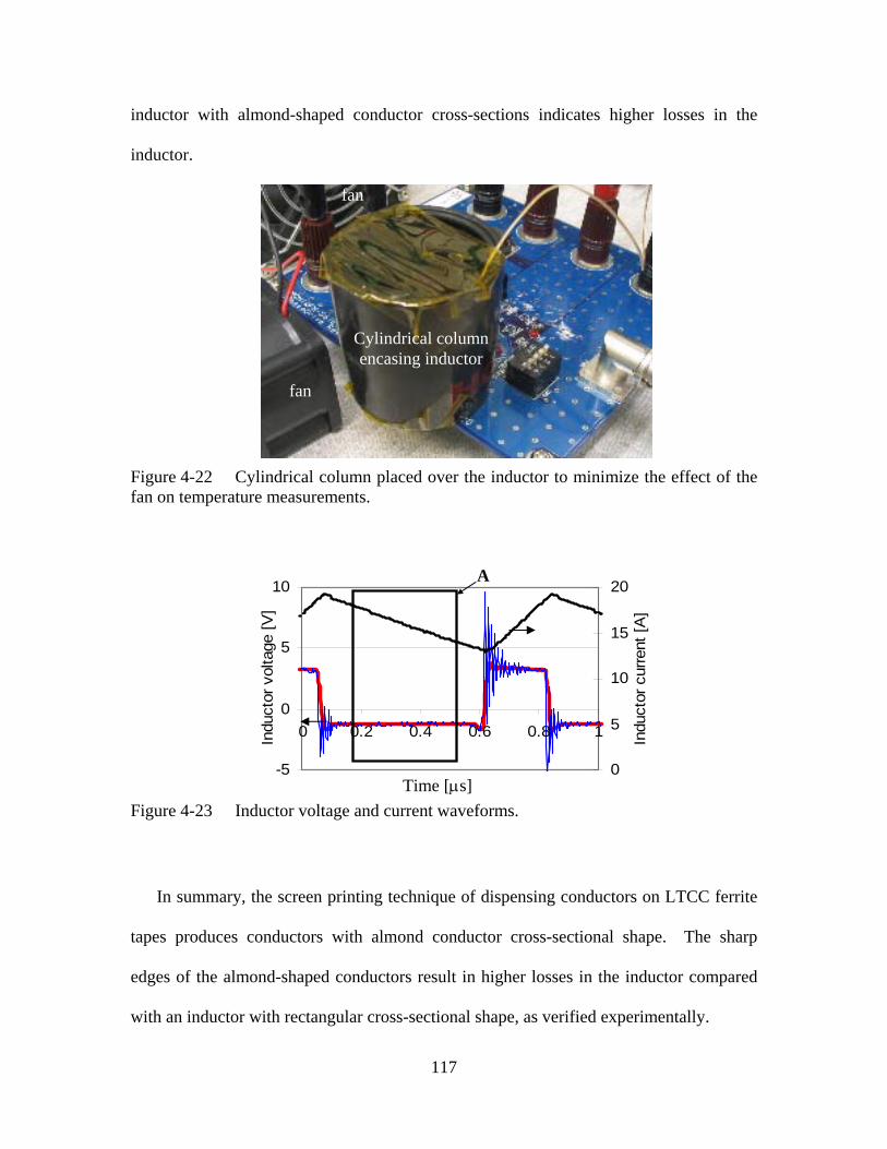
117
inductor with almond-shaped conductor cross-sections indicates higher losses in the
inductor.
In summary, the screen printing technique of dispensing conductors on LTCC ferrite
tapes produces conductors with almond conductor cross-sectional shape. The sharp
edges of the almond-shaped conductors result in higher losses in the inductor compared
with an inductor with rectangular cross-sectional shape, as verified experimentally.
Cylindrical column encasing inductor
Figure 4-22 Cylindrical column placed over the inductor to minimize the effect of the fan on temperature measurements.
fan
fan
-5
0
5
10
0 0.2 0.4 0.6 0.8 1
time [us]
Indu
ctor
vol
tage
[V]
0
5
10
15
20
Indu
ctor
cur
rent
[A]
A
Figure 4-23 Inductor voltage and current waveforms. Time [μs]

118
4.4 Circuit Specifications for Chip Inductor
The inductors are tested in a prototype 5 V - to - 1.1 V buck converter (see Fig. 4-9)
operating at a switching frequency of 4 MHz. The devices used are integrated in a
multichip module, DrMOS from Renesas [119]. The integrated top MOSFET (Q2) is
HAT2168 and the bottom MOSFET (Q1) is HAT2165. The full load current is 12.5 A.
The input voltage of the gate drive is 5 V, which is provided by the Agilent E3631A. The
pulse width modulation (PWM) input is provided by means of a 20 MHz Agilent function
generator 33220A. The power supply for the power stage is provided by the Lambda
UP6-132 DC power supply. Four Fluke 45 dual display digital multi-meters are used to
measure the input and output voltages as well as currents.
A shunt is connected between the power supply and the input node of the buck
converter circuit for the purpose of measuring the input current. Another shunt is
connected between the output and the ground for measuring the output current. The
Figure 4-24 Inductance and temperature rise comparison for the rectangular and almond conductor cross-sectional shapes at full load (IDC = 5A).
0
5
10
15
20
25
30
Rect Almd
Cross-sectional shape of conductors
Tris
e [C
]
0
10
20
30
40
50
60
Indu
ctan
ce [n
H]
Trise
L
Tem
pera
ture
rise
[°C
]
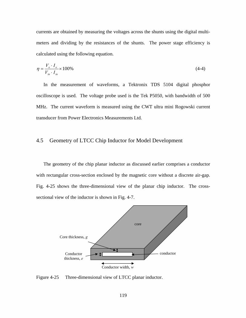
119
currents are obtained by measuring the voltages across the shunts using the digital multi-
meters and dividing by the resistances of the shunts. The power stage efficiency is
calculated using the following equation.
%100×⋅⋅
=inin
oo
IVIV
η (4-4)
In the measurement of waveforms, a Tektronix TDS 5104 digital phosphor
oscilloscope is used. The voltage probe used is the Tek P5050, with bandwidth of 500
MHz. The current waveform is measured using the CWT ultra mini Rogowski current
transducer from Power Electronics Measurements Ltd.
4.5 Geometry of LTCC Chip Inductor for Model Development
The geometry of the chip planar inductor as discussed earlier comprises a conductor
with rectangular cross-section enclosed by the magnetic core without a discrete air-gap.
Fig. 4-25 shows the three-dimensional view of the planar chip inductor. The cross-
sectional view of the inductor is shown in Fig. 4-7.
Figure 4-25 Three-dimensional view of LTCC planar inductor.
core
conductor
Conductor width, w
Conductor thickness, e
Core thickness, g

120
4.6 Parametric Variation of Inductor Geometry
The variation in permeability due to saturation and the resulting change in magnetic
path length establish a complex relationship between the material properties, geometry,
current and inductance. Yet, an adequate quantitative model for inductance variation
does not exist. It was therefore decided to carry out geometry variation experiments to
study the effect of the inductor geometry on the circuit performance, particularly the light
load efficiency. The effect of varying the number of parallel conductors of the planar
inductor and the conductor width on the overall efficiency of the converter, particularly
the light load efficiency, are studied. This variation experiment can serve as a guide in
designing the filter inductor according to the requirements and tradeoffs between light
load efficiency and transient performance of the converter. It also serves to evaluate
whether the LTCC processing and manufacturing of the inductor needs to be changed,
since dimensions can influence temperature profiles, laminating pressures and warping
during firing. For all the variation experiments, the full load inductance is kept constant,
so that the inductor current ripple at full load is kept constant. This implies that the
switching and gate driver losses are kept constant at full load. The effects of inductor
geometry on light load efficiency are then compared.
4.6.1 Effect of Varying Conductor Width
In this set of experiments, the conductor width of a single conductor inductor is
varied to study its effect on light load efficiency of the converter. The conductor width of
the inductor is varied between 1 mm to 5 mm, with the dimensions defined as in Fig. 4-

121
26. The dashed line indicates the position of the embedded conductor of the inductor.
Fig. 4-27 shows the cross-sectional view of the inductors with different conductor widths
ranging from 1 mm to 5 mm. The fabrication procedure in section 2.4.7 as described in
association with Fig. 2-20 is not affected.
Fig. 4-28 shows the change in inductance with output current for the various
inductors with conductor widths ranging from 1mm to 5mm. It is observed that as
inductor width decreases, the change in inductance with output current increases.
Figure 4-27 Cross-sectional view of LTCC inductors with conductor widths ranging from 1 mm to 5 mm.
0.40 mm
core
core
core
Alumina tile for comparison 125 μm
4.98 mm
conductor
conductor
2.02 mm
0.40 mm
0.41 mm
conductor
4.11 mm conductor
1.12 mm
core
0.40 mm
l
w
Figure 4-26 Dimensions of LTCC inductor.

122
Figure 4-29(a) shows the comparison of light load inductor current waveforms for
LTCC inductor with a conductor width of 1 mm, and the two commercial 47 nH air-
gapped inductors connected in parallel, named as 23 nH inductor as a benchmark. Fig. 4-
29(b) shows the comparison of inductor current waveforms of the two inductors at a full
load current of 12.5 A. It is clear that the current ripple associated with these two types
of inductors at this current is similar.
-3-2-1012345
0 0.1 0.2 0.3 0.4 0.5
time [us]
Indu
ctor
cur
rent
[A]
w =1mm inductor23nH inductor(a) Time [μs]
Figure 4-28 Change of inductance with output current.
102030405060708090
0 2 4 6 8 10 12 14 16Output current [A]
Indu
ctan
ce [n
H]
w=1mmw=2mmw=3mmw=4mmw=5mm23nH inductor
12.5A1A

123
The substantial reduction in the inductor ripple current at light load is attributed to the
higher inductance value of the LTCC inductor with conductor width, w, of 1 mm at light
load. This results in an increase in light load efficiency of the converter, as evident in
Fig. 4-30(a). At a light load current of 1 A, the efficiency can be improved by greater
than 15 %. When the load current decreases to 0.5 A, the efficiency can be improved by
greater than 30 %. Fig. 4-30(b) shows the heavy load efficiency comparison. At a full
load current of 12.5 A, the difference in power stage efficiency is kept to within 2 %.
Above this current, it is evident that the decreasing tendency of the efficiency for a
conductor width of 5 mm differs from the other curves. We conclude that this is not due
to increased inductor losses. It is to be noted here that the full load inductance for the
inductor with conductor width 1mm (31 nH) is larger than that for the inductor with
conductor width 5 mm (18.5 nH). This implies that the all important semiconductor
switching losses in the circuit will be higher for the inductor with conductor width 5 mm
and continue to increase, since the inductance continues to decrease, as shown in Fig. 4-
8
10
12
14
16
18
20
0 0.1 0.2 0.3 0.4 0.5time [us]
Indu
ctor
cur
rent
[A] w =1mm inductor
23nH inductor
Figure 4-29 Inductor current waveforms comparison (a) at light load current of 1 A and (b) at full load current of 12.5 A, for LTCC inductor with conductor width 1 mm and commercial inductor of effective inductance 23 nH. Vin = 5 V, Vo = 1.1 V.
(b) Time [μs]

124
28. This is not the case for the commercial benchmark inductor, see Fig. 4-28.
Consequently, the inductor with conductor width, w, of 5 mm becomes inferior to the
benchmark due to these circuit considerations above this current, presenting a limiting
case for our study. It should also be noted in this context that the losses in the conductors
have little influence on the overall system efficiency, see the discussion of Fig. 3-34. In
terms of system efficiency, these losses are found to be negligible, see section 4.6.3. On
the other hand, the inductor with wider conductor width has lower conduction loss
compared with the inductor with narrow conductor width. Therefore, it is difficult to
decouple these two effects by using this analysis alone.
Although narrow LTCC inductors show higher efficiency at light load, it is often at
the detriment of full load efficiency, as a result of having higher ohmic resistance. At a
full load current of 12.5 A, it is observed that the efficiency drops by around 2 %,
compared with using the 23 nH commercial air-gapped inductor (two 47 nH commercial
inductors connected in parallel). This translates to an additional 275 mW resistive loss at
a full load current of 12.5 A, in the inductor due to higher ohmic resistance. However,
this loss is still small compared to the losses in the active devices. One way to solve this
problem is a reduction of the resistivity of the conductor material.
In summary, it is found that by reducing the conductor width of the inductor increases
the change in inductance with load current. For this inductor structure without a discrete
air gap, as DC current increases, the core adjacent to the conductor starts to saturate.
This causes the average magnetic path length to increase. This increase in the average
magnetic path length becomes more pronounced when the conductor width of the
inductor decreases, which helps to bring about the non-linear behavior of the inductor.
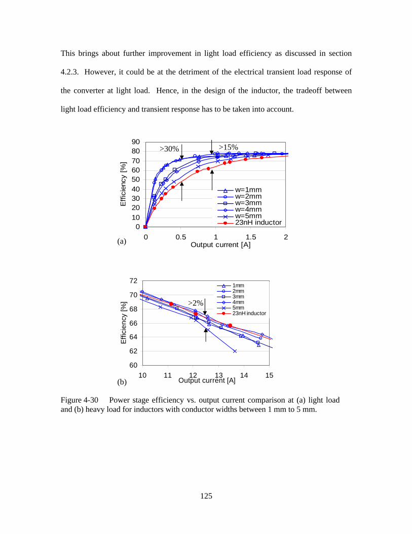
125
This brings about further improvement in light load efficiency as discussed in section
4.2.3. However, it could be at the detriment of the electrical transient load response of
the converter at light load. Hence, in the design of the inductor, the tradeoff between
light load efficiency and transient response has to be taken into account.
60
62
64
66
68
70
72
10 11 12 13 14 15Output current [A]
Effic
ienc
y [%
]
1mm2mm3mm4mm5mm23nH inductor
Figure 4-30 Power stage efficiency vs. output current comparison at (a) light load and (b) heavy load for inductors with conductor widths between 1 mm to 5 mm.
>2%
(b)
0102030405060708090
0 0.5 1 1.5 2Output current [A]
Effi
cien
cy [%
]
w=1mmw=2mmw=3mmw=4mmw=5mm23nH inductor
>15%>30%
(a)
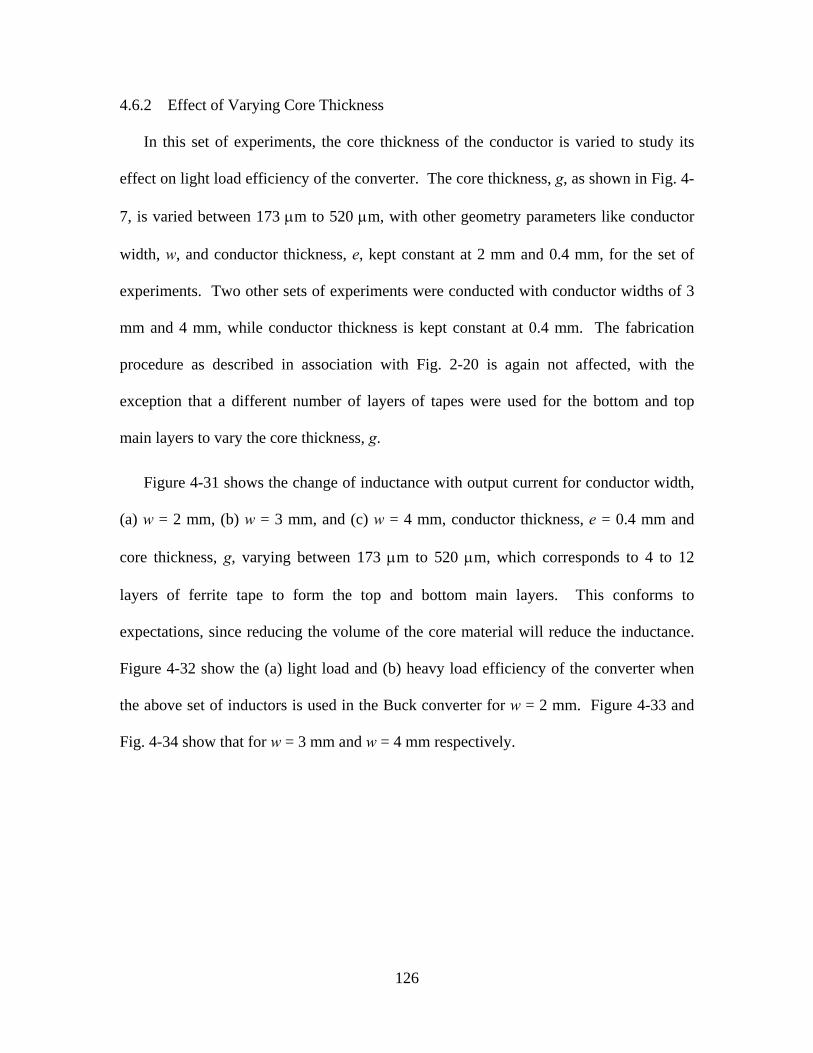
126
4.6.2 Effect of Varying Core Thickness
In this set of experiments, the core thickness of the conductor is varied to study its
effect on light load efficiency of the converter. The core thickness, g, as shown in Fig. 4-
7, is varied between 173 μm to 520 μm, with other geometry parameters like conductor
width, w, and conductor thickness, e, kept constant at 2 mm and 0.4 mm, for the set of
experiments. Two other sets of experiments were conducted with conductor widths of 3
mm and 4 mm, while conductor thickness is kept constant at 0.4 mm. The fabrication
procedure as described in association with Fig. 2-20 is again not affected, with the
exception that a different number of layers of tapes were used for the bottom and top
main layers to vary the core thickness, g.
Figure 4-31 shows the change of inductance with output current for conductor width,
(a) w = 2 mm, (b) w = 3 mm, and (c) w = 4 mm, conductor thickness, e = 0.4 mm and
core thickness, g, varying between 173 μm to 520 μm, which corresponds to 4 to 12
layers of ferrite tape to form the top and bottom main layers. This conforms to
expectations, since reducing the volume of the core material will reduce the inductance.
Figure 4-32 show the (a) light load and (b) heavy load efficiency of the converter when
the above set of inductors is used in the Buck converter for w = 2 mm. Figure 4-33 and
Fig. 4-34 show that for w = 3 mm and w = 4 mm respectively.
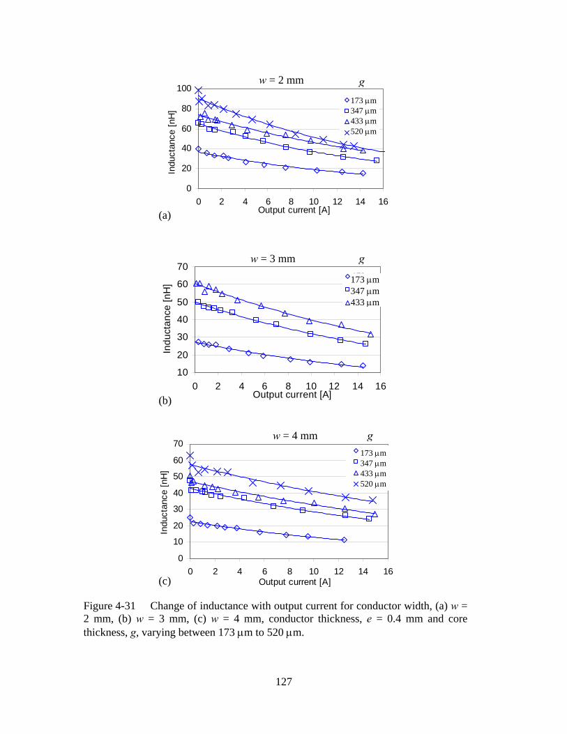
127
10
20
30
40
50
60
70
0 2 4 6 8 10 12 14 16Output current [A]
Indu
ctan
ce [n
H]
173um
347um
433um
g
(b)
w = 3 mm
173 μm 347 μm 433 μm
0
10
20
30
40
50
60
70
0 2 4 6 8 10 12 14 16Output current [A]
Indu
ctan
ce [n
H]
173um347um433um520um
Figure 4-31 Change of inductance with output current for conductor width, (a) w = 2 mm, (b) w = 3 mm, (c) w = 4 mm, conductor thickness, e = 0.4 mm and core thickness, g, varying between 173 μm to 520 μm.
(c)
gw = 4 mm173 μm 347 μm433 μm520 μm
0
20
40
60
80
100
0 2 4 6 8 10 12 14 16Output current [A]
Indu
ctan
ce [n
H]
173um347um433um520um
g
(a)
w = 2 mm
173 μm 347 μm433 μm520 μm

128
7072747678808284
10 12 14 16 18Output current [A]
Effi
cien
cy [%
]
173um
347um
433um
520um
Figure 4-32 Power stage efficiency vs. output current comparison at (a) light loadand (b) heavy load for core thickness variation between 173 μm to 520 μm for w = 2 mm.
g
(b)
w = 2 mm
173 μm 347 μm 433 μm 520 μm
0
20
40
60
80
100
0 0.5 1 1.5 2Output current [A]
Effi
cien
cy [%
]
173um
347um
433um
g
(a)
w = 3 mm
173 μm 347 μm 433 μm
0
20
40
60
80
100
0 0.5 1 1.5 2Output current [A]
Effi
cien
cy [%
]
173um
347um
433um
520um
g
(a)
173 μm 347 μm 433 μm 520 μm
w = 2 mm

129
From the efficiency curves, it is apparent that the inductor with thinner core has
significantly lower overall efficiency, which is attributed to its significantly lower
inductance. As a result, the ripple current is large, leading to larger losses in the
switches. For inductors with core thickness varying from 347 μm to 520 μm, the
efficiency curves are similar, though the inductor current ripple difference is close to 40
%. This implies that there is a critical core thickness (inductance value), beyond which,
there is no significant improvement in power stage efficiency This is because, beyond
the critical core thickness, as core thickness increases, inductance increases, which leads
to a decrease in switching losses in the MOSFETs due to a smaller current ripple.
However, core losses in the inductor increases due to increased core volume, which
negates the effect of the decrease in switching losses. The other two sets of inductors
with core thickness varying between 173 μm to 520 μm, keeping conductor widths
constant at 3 mm and 4 mm respectively, show similar results.
70727476
78808284
10 12 14 16 18Output current [A]
Effi
cien
cy [%
]
173um
347um
433um
Figure 4-33 Power stage efficiency vs. output current comparison at (a) light loadand (b) heavy load for core thickness variation between 173 μm to 520 μm for w = 3 mm.
g
(b)
w = 3 mm
173 μm 347 μm 433 μm

130
In summary, sufficient core thickness is necessary to increase the inductance of the
inductor. Low inductance value is detrimental from the power loss point of view. There
seems to be a critical inductance value, whereby increasing the inductance further, does
not result in significant improvement in power stage efficiency especially at low power.
This is circuit related and will not be discussed further in this dissertation.
4.6.3 Effect of Varying Conductor Thickness
Increased conductor thickness is necessary to decrease the DC resistance of the
inductor. In this set of experiments, the conductor thickness is varied to observe its effect
70
7274
7678
8082
84
10 11 12 13 14 15 16Output current [A]
Effi
cien
cy [%
]
173um
347um
433um
520um
Figure 4-34 Power stage efficiency vs. output current comparison at (a) light load and (b) heavy load for core thickness variation between 173 μm to 520 μm for w = 4 mm.
g
(b)
w = 4 mm173 μm 347 μm 433 μm 520 μm
0
20
40
60
80
100
0 0.5 1 1.5 2Output current [A]
Effi
cien
cy [%
]
173um
347um
433um
520um
g
(a)
w = 4 mm
173 μm 347 μm 433 μm 520 μm
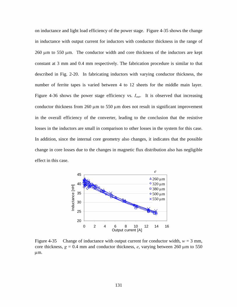
131
on inductance and light load efficiency of the power stage. Figure 4-35 shows the change
in inductance with output current for inductors with conductor thickness in the range of
260 μm to 550 μm. The conductor width and core thickness of the inductors are kept
constant at 3 mm and 0.4 mm respectively. The fabrication procedure is similar to that
described in Fig. 2-20. In fabricating inductors with varying conductor thickness, the
number of ferrite tapes is varied between 4 to 12 sheets for the middle main layer.
Figure 4-36 shows the power stage efficiency vs. Iout. It is observed that increasing
conductor thickness from 260 μm to 550 μm does not result in significant improvement
in the overall efficiency of the converter, leading to the conclusion that the resistive
losses in the inductors are small in comparison to other losses in the system for this case.
In addition, since the internal core geometry also changes, it indicates that the possible
change in core losses due to the changes in magnetic flux distribution also has negligible
effect in this case.
20
25
30
35
40
45
0 2 4 6 8 10 12 14 16Output current [A]
Indu
ctan
ce [n
H]
260um320um380um500um550um
Figure 4-35 Change of inductance with output current for conductor width, w = 3 mm, core thickness, g = 0.4 mm and conductor thickness, e, varying between 260 μm to 550 μm.
e 260 μm 320 μm 380 μm 500 μm 550 μm

132
4.6.4 Effect of Varying Number of Parallel Conductors
It is known that multiple conductors in parallel, with each conductor surrounded by
an electrically insulated magnetic material, helps to alleviate current crowding at the two
sides of a rectangular conductor. This is due to partial magnetic isolation of the
conductors, which reduces proximity effect between the conductors. Besides, it is also of
interest to find out whether there will be an appreciable difference in the inductance
change with load current, and the effect of multi-conductor inductor on converter
performance, particularly the light load efficiency. In this section, the inductors are
investigated with different numbers of parallel conductors, ranging from 1 to 3. They are
designed to have similar inductance values at full load. The effect of having different
numbers of parallel conductors is studied, particularly the impact on converter efficiency
at both light load and heavy load. The footprint of the inductors is kept constant, and the
same as the single conductor inductor in order to have a fair packaging comparison.
0
20
40
60
80
100
0 5 10 15Current [A]
Effi
cien
cy [%
]
182um267um347um440um540um
Figure 4-36 Power stage efficiency vs. output current using inductors with conductorwidth, w = 3 mm, core thickness, g = 0.4 mm and conductor thickness, e, varying between 260 μm to 550 μm.
e 260 μm 320 μm 380 μm 500 μm 550 μm

133
In the design of the multi-conductor inductor, the conductor width is used to vary the
inductance value. In order to obtain a similar inductance value for the inductors with
different number of parallel conductors, the width of each conductor for an inductor with
3-parallel conductors will be narrower than that of an inductor with 2-parallel conductors.
It is also noted here that in order to obtain a similar inductance at full load, the total
conductor cross-sectional area may not be the same. Since an appropriate quantitative
model does not yet exist, we estimated the desired conductor widths by trial and error.
Figure 4-37 shows the change in inductance with output current for LTCC inductors
with number of parallel conductors, n = 1 to n = 3, in comparison with the commercial
discrete air-gap surface mount 23nH inductor. The LTCC inductors are designed to have
a full load inductance value similar to that of the commercial inductor. However, it is
noted here that at a full load current of 12.5A, the inductance of the LTCC inductors are
lower than expected. This is due to inaccuracy in the dimensional control during the
inductor fabrication process and can be improved in future. The lower inductance value
at full load will result in lower full load converter efficiency.
20
25
30
35
40
45
0 2 4 6 8 10 12 14 16Output current [A]
Indu
ctan
ce [n
H]
n=1n=2n=323nH inductor
12.5A1A
Figure 4-37 Change of inductance with output current.
134
Figure 4-38(a) shows the power stage efficiency at light load and Fig. 4-38(b) shows
the efficiency at heavy load. The light load efficiency does not vary much with the
number of parallel conductors. Besides, the improvement in light load efficiency is also
evident, as illustrated by the greater than 10% improvement in efficiency at a light load
current of 1 A. That this value is lower than the previously found improvement with the
single conductor inductors is attributable to the lower inductance at light load for the
multi-conductor case, as indicated when comparing Fig. 4-37 to Fig. 4-28. At heavy
load, there is also no obvious change in efficiency with the number of parallel
conductors. However, it is observed that the heavy load converter efficiency is lower for
the LTCC inductors. This is due to the increased switching losses, attributable to the
unexpected lower inductance of the LTCC inductors at full load, which has been
explained previously.
In summary, varying the number of parallel conductors (between 1 and 3) within the
same footprint does not result in an appreciable difference in the inductance change with
load current. Hence, there is also no observable change in light load or heavy load
efficiency when LTCC inductors with different number of parallel conductors are used,
under the constraint of a footprint equal to 8 mm x 20 mm.

135
4.7 Inductance Model for LTCC Inductor
An empirical model has been developed for an inductor structure with a rectangular
conductor embedded in the magnetic material (see Fig. 4-7). The model relates
inductance with the geometry factors of the inductor as well as its magnetic permeability,
given by equation (4-5) [47].
60
62
64
66
68
70
10 11 12 13 14 15Output current [A]
Effi
cien
cy [%
]
n=1n=2n=323nH inductor
(b)
Figure 4-38 Power stage efficiency vs. output current comparison at (a) light loadand (b) heavy load, for multi-conductor inductor.
0
20
40
60
80
0 0.5 1 1.5 2Output current[A]
Effi
cien
cy [%
]
n=1n=2n=323nH inductor
>10%
(a)
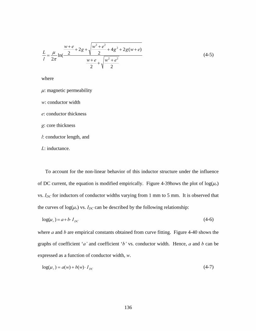
136
22
)(242
22ln(
2 22
222
ewew
ewggewgew
lL
++
+
++++
+++
=πμ (4-5)
where
μ: magnetic permeability
w: conductor width
e: conductor thickness
g: core thickness
l: conductor length, and
L: inductance.
To account for the non-linear behavior of this inductor structure under the influence
of DC current, the equation is modified empirically. Figure 4-39hows the plot of log(μr)
vs. IDC for inductors of conductor widths varying from 1 mm to 5 mm. It is observed that
the curves of log(μr) vs. IDC can be described by the following relationship:
DCr Iba ⋅+=)log(μ (4-6)
where a and b are empirical constants obtained from curve fitting. Figure 4-40 shows the
graphs of coefficient ‘a’ and coefficient ‘b’ vs. conductor width. Hence, a and b can be
expressed as a function of conductor width, w.
DCr Iwbwa ⋅+= )()()log(μ (4-7)

137
Core thickness g, as shown in Fig. 4-7, is varied, and the graph of log(μr) vs. IDC is
plotted in Fig. 4-41 (a), (b), and (c) for conductor widths of 2 mm, 3 mm, and 4 mm. It is
observed that the change in log(μr) with IDC is independent of the change in core
thickness. Since the conductors are of the same dimensions for the samples with various
core thicknesses, the average magnetic path length would be similar, which will result in
y = 0.0041x - 0.0365
y = 0.022x + 1.694
1.68
1.72
1.76
1.8
1.84
0 1 2 3 4 5 6conductor w idth [mm]
a(w
)
-0.04
-0.03
-0.02
-0.01
0
b(w
)
Figure 4-40 Graph of coefficient ‘a(w)’ and ‘b(w)’ of equation (4-7) vs. conductor width.
1.11.21.31.41.51.61.71.81.9
0 5 10 15 20DC current [A]
log(
Ur)
1mm2mm3mm4mm5mm
Figure 4-39 Graph of log(μr) vs. IDC for inductors of conductor widths varying from 1 mm to 5 mm.
w

138
a similar magnetic flux density distribution in the core. The increase in core thickness
will increase the inductance, but it has little impact on the effective permeability.
Conductor thickness e, shown in Fig. 4-7, is varied, and the graph of log(μr) vs. IDC is
plotted in Fig. 4-42. It is observed that the change in log(μr) with IDC is independent of
the change in conductor thickness. Since the conductor width is much larger than the
conductor thickness, as long as the increase in conductor thickness is much smaller than
the conductor width, the average magnetic path length would be similar for all the
samples. This results in a similar magnetic flux density distribution in the core for all the
samples, resulting in a similar effective permeability.
1.4
1.5
1.6
1.7
1.8
0 5 10 15 20DC current [A]
lg(U
r)
173um
347um
433um
g
(b)
w = 3 mm
173 μm 347 μm 433 μm
1.2
1.3
1.4
1.5
1.6
1.7
1.8
1.9
0 5 10 15 20DC current [A]
lg(U
r)
173um
347um
433um
520um
(a)
g w = 2 mm
173 μm 347 μm 433 μm 520 μm

139
Based on the results obtained above, an empirical model for the LTCC inductor is
developed as shown in equation (4-8).
)
22
)(242
22ln(
2 22
222
0
ewew
ewggewgewU
lL r
++
+
++++
+++
=πμ (4-8)
where )4.46(037.0)4.5(410 DCDC IIwrU −++= .
1.4
1.5
1.6
1.7
1.8
0 5 10 15DC current [A]
lg(U
r)
182um267um347um440um540um
Figure 4-42 Graph of log(μr) vs. IDC for inductors of various conductor thickness, e.
e 260 μm 320 μm 380 μm 500 μm 550 μm
1.3
1.4
1.5
1.6
1.7
1.8
0 5 10 15 20DC current [A]
lg(U
r)
173um
347um
433um520um
g
(c) Figure 4-41 Graph of log(μr) vs. IDC for inductors of various core thickness, g, for conductor widths of (a) 2 mm and (b) 3 mm and (c) 4 mm.
w = 4 mm
173 μm 347 μm 433 μm 520 μm

140
This empirical model is developed based on LTCC inductors fabricated using the
low-permeability (μr = 60 from datasheet) LTCC magnetic tape purchased from
Electroscience Labs [28]. This model is valid for LTCC planar inductors fabricated using
the low-permeability tape with conductor widths between 1 mm to 4 mm, conductor
thickness 180 μm to 550 μm, and core thickness 170 μm to 520 μm, measured at a
switching frequency of 4 MHz DC current from 0 A to 16 A. Since the above model is
developed based on the low-permeability LTCC ferrite tape purchased from
Electroscience Labs, it is not applicable for other ferrites. For inductors made using other
ferrites, the same methodology can be used to obtain the empirical model.
4.8 Inductor Design Procedure
In section 4.7, an empirical model for LTCC inductors fabricated using the low
permeability tape purchased from Electroscience Labs [28] has been developed. In this
section, the inductor design procedure will be described and will be illustrated with a
design example, followed by actual fabrication and experimental verification. Fig. 4-43
shows the design flow diagram.
1. Obtain inputs
Table 4-2 shows the specifications of an example in designing an inductor using the
above empirical model. The conductivity of the Ag/Pt paste is estimated to be 1.7 × 10⁷
S/m, as discussed in Chapter 3. Figure 4-44 shows the position where the inductor
electrodes must lie and the given footprint of the inductor.

141
1. Obtain inputs: thickness, t, footprint, IDC, L0, σ
)(2
)(
)(we
nwwl
wRcorner
⋅
+=
σ
oLewL =]1[),(
3. Express L as a function of conductor width, w, and conductor thickness, e. Equate to L0.
4. Plot e(w) vs w
2)( eteg −=
8. Obtain corresponding e, g, l, R values
7. Obtain w at minimum point
6. Plot R(w) vs. w and curve fit using 8th order polynomial
Figure 4-43. Flow diagram for LTCC inductor design.
2. Express core thickness as a function of conductor thickness, e
5. Express winding resistance, R, as a function of w.

142
2. Express core thickness as a function of conductor thickness, e
Since the magnetic core surrounds the conductor, as in Fig. 4-7, core thickness, t, can
be expressed as a function of conductor thickness, e,
2)( eteg −= (4-9)
Table 4-2 Specifications for inductor
L0 [nH] 25
IDC [A] 12.5
Distance between electrodes [mm] 10
Thickness [mm] 1
3. Express L as a function of conductor width, w, and conductor thickness, e. Equate
to L0.
Ur in equation (4-8) is expressed as a function of conductor width, w
)4.46(037.0)4.5(410 DCDC IIwrU −++=
12.16.8510)( += wr wU (4-10)
Equation (4-8) is then expressed as a function of w and e, and equated to L0.
Figure 4-44 Footprint of the inductor and the position of the electrodes.
10 mm Electrodes of
inductor
Footprint of inductor
Board
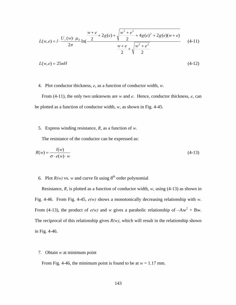
143
22
))((2)(42
)(22ln(
2)(
),(22
222
0
ewew
ewegegewegewwU
lewL r
++
+
++++
+++
⋅⋅=
πμ (4-11)
nHewL 25),( = (4-12)
4. Plot conductor thickness, e, as a function of conductor width, w.
From (4-11), the only two unknowns are w and e. Hence, conductor thickness, e, can
be plotted as a function of conductor width, w, as shown in Fig. 4-45.
5. Express winding resistance, R, as a function of w.
The resistance of the conductor can be expressed as:
wwewlwR
⋅⋅=
)()()(
σ (4-13)
6. Plot R(w) vs. w and curve fit using 8th order polynomial
Resistance, R, is plotted as a function of conductor width, w, using (4-13) as shown in
Fig. 4-46. From Fig. 4-45, e(w) shows a monotonically decreasing relationship with w.
From (4-13), the product of e(w) and w gives a parabolic relationship of –Aw2 + Bw.
The reciprocal of this relationship gives R(w), which will result in the relationship shown
in Fig. 4-46.
7. Obtain w at minimum point
From Fig. 4-46, the minimum point is found to be at w = 1.17 mm.

144
Figure 4-45 Graph of conductor thickness, e, vs. conductor width, w, for L = 25 nH.
0.2 0.4 0.6 0.8 1 1.2 1.4 1.6 1.80.1
0.2
0.3
0.4
0.5
0.6
Conductor width, w [mm]
Con
duct
or th
ickn
ess,
e [
mm
]
datacurve fit
Figure 4-46 Graph of resistance, R, vs. conductor width, w.
0.2 0.4 0.6 0.8 1 1.2 1.4 1.6 1.81
1.5
2
2.5
3
3.5
4
4.5
5
Conductor width, w [mm]
Res
ista
nce,
R [m
Ω]
datacurve fit

145
8. Obtain corresponding e, g, l, R values
Winding resistance, R(w), can be obtained from (4-13). Conductor thickness e(w) can
be obtained from (4-11) and (4-12). Core thickness, g(e), can be obtained from (4-9).
Table 4-3 tabulates the design values of e, g, l, w and R for L0 = 25 nH.
Table 4-3 Inductor Design Values
L [nH] e [mm] g [mm] l [mm] w [mm] R [Ω]
25 0.348 0.326 10.0 1.17 1.44
4.9 Summary
It is shown that LTCC technology is a very promising technology for the integration
of power electronics applications. Based on the inductor geometries discussed in section
4.2, the short winding inductor with magnetic core enclosing the conductor, gives the
flexibility in varying the conductor’s cross-sectional area, which makes it suitable for
achieving low DC resistance and high current capability.
Conductors with elongated almond cross-sectional shape, which are characteristic of
screen printed conductors, are undesirable for high frequency applications from the
conduction loss point of view. The overall power loss becomes greater when the
conductor is surrounded by magnetic material, as verified by simulation, as well as
experimentally. Hence, it is desirable to alter the conventional method of screen printing
conductor paste on LTCC green tape to obtain a rectangular conductor cross-sectional
shape for applications in which power loss is to be minimized. In addition, from the

146
point of view of footprint occupied by the conductor, conductors with rectangular
conductor cross-section offer the potential to obtain a much smaller footprint compared to
conductors with almond cross-sectional shapes.
In the parametric variation of inductor geometry, it is found that by reducing the
conductor width of the inductor increases the change in inductance with load current. For
this inductor structure without a discrete air gap, as DC current increases, the core
adjacent to the conductor starts to saturate, which causes the average magnetic path
length to increase. This increase in the average magnetic path length becomes more
pronounced when the conductor width of the inductor decreases, which results in the non-
linear behavior of the inductor. This brings about further improvement in light load
efficiency as discussed in section 4.2.3.
An empirical model is subsequently developed based on LTCC inductors fabricated
using the low-permeability (μr = 60 from datasheet) LTCC magnetic tape purchased from
Electroscience Labs [28]. This model is valid for LTCC planar inductors fabricated using
the low-permeability tape with conductor widths between 1 mm to 4 mm, conductor
thickness 260 μm to 550 μm, and core thickness 173 μm to 520 μm, measured at a
switching frequency of 4 MHz DC current from 0 A to 16 A. Since the above model is
developed based on the low-permeability LTCC ferrite tape purchased from
Electroscience Labs, it is not applicable for other ferrites. For inductors made using other
ferrites, the same methodology can be used to obtain the empirical model. An inductor
design flow diagram has been formulated to help in the design of such inductors. An
inductor design example is shown to demonstrate the use of the design flow diagram.
147
Chapter 5. LTCC Inductor as Substrate
5.1 Overview
The popularity of portable devices makes size reduction necessary to decrease the
dimensions of the overall system. In a dc-dc converter, the bulkiest components are the
capacitors and the inductors. In the previous chapter, the manufacturing and design of
low profile (1 mm) chip inductors have been investigated as a first step in size reduction
of these DC-DC converters. Configuring the inductor as the substrate carrying the
semiconductor and the other electronic components is a next step as a means to mitigate
the negative impact of inductor size on power density and is investigated in this chapter.
As the conductive traces are placed in the proximity of the magnetic substrate, however,
the parasitic trace inductances increase, adversely affecting circuit operation. A solution
to this problem by introducing a conductive shield between the inductor as substrate and
the active circuitry is also addressed in this chapter.
It is investigated that the presence of a metal shield reduces trace inductances and
improves circuit performance and shows that there is a minimum shield thickness
required to minimize losses associated with ringing. The role of shield conductivity is to
lower the trace inductance and minimize power loss, as well as the positioning of the
shield to minimize inductance, is investigated.
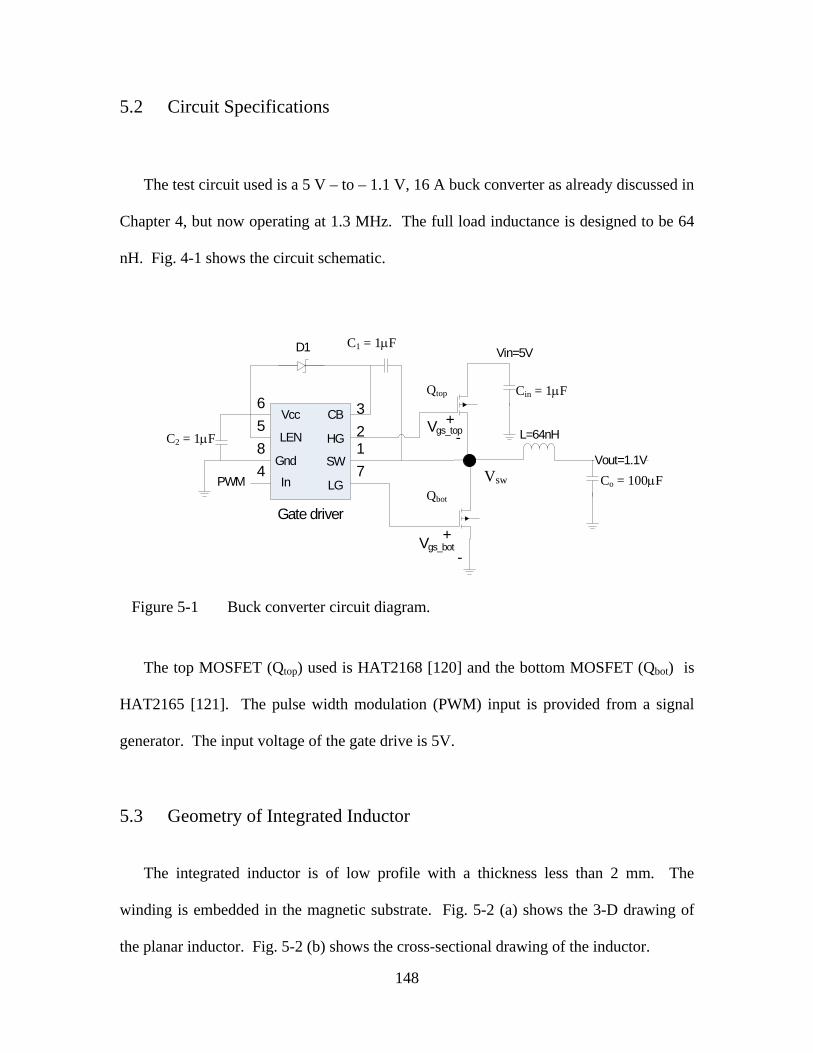
148
5.2 Circuit Specifications
The test circuit used is a 5 V – to – 1.1 V, 16 A buck converter as already discussed in
Chapter 4, but now operating at 1.3 MHz. The full load inductance is designed to be 64
nH. Fig. 4-1 shows the circuit schematic.
The top MOSFET (Qtop) used is HAT2168 [120] and the bottom MOSFET (Qbot) is
HAT2165 [121]. The pulse width modulation (PWM) input is provided from a signal
generator. The input voltage of the gate drive is 5V.
5.3 Geometry of Integrated Inductor
The integrated inductor is of low profile with a thickness less than 2 mm. The
winding is embedded in the magnetic substrate. Fig. 5-2 (a) shows the 3-D drawing of
the planar inductor. Fig. 5-2 (b) shows the cross-sectional drawing of the inductor.
Bootstrap capacitor
Figure 5-1 Buck converter circuit diagram.
Co=100uF
L=64nH
Vout=1.1V
236
584 7
1
CB
HG
SW
LG
Vcc
LEN
In
Gnd
Qtop
Qbot
C2=1uF
Vin=5V
PWM
D1 C1=1uF
Vgs_top
Vgs_bot+
-
+-
Cin=1uF
Gate driver
C1 = 1μF
Cin = 1μF
C2 = 1μF
Co = 100μF Vsw
Qtop
Qbot

149
5.4 Substrate Inductor Design Procedure
In section 4.7, an empirical model for LTCC inductors fabricated using the low
permeability tape purchased from Electroscience Labs [28] was developed. In this
section, the inductor design procedure will be described and will be illustrated with a
design example, followed by actual fabrication and experimental verification of its
properties. Fig. 5-3 shows the design flow diagram.
conductor
g
g e
w
core
Figure 5-2 LTCC inductor substrate. (a) Three-dimensional view of LTCC planar inductor, (b) cross-sectional diagram of LTCC planar inductor.
core
Conductor width, w
Conductor thickness, e
Core thickness, g
(a)
(b)
conductor
t

150
1. Obtain inputs: thickness, t, footprint, IDC, L0, σ
2. Express conductor length as a function of w (exclude corners), l(w),
)(2
)(
)(we
nwwl
wRcorner
⋅
+=
σ
oLewL =]1[),(
4. Express L as a function of conductor width, w, and conductor thickness, e. Equate to L0.
5. Plot e(w) vs w
2)( eteg −=
9. Obtain corresponding e, g, l, R values
8. Obtain w at minimum point
7. Plot R(w) vs. w and curve fit using 8th order polynomial
Figure 5-3. Flow diagram for LTCC inductor substrate design.
3. Express core thickness as a function of conductor thickness, e
5. Express winding resistance, R, as a function of w.

151
1. Obtain inputs
Table 5-1 shows the specifications of an example in designing an inductor using the
above empirical model. The conductivity of the Ag/Pt paste is estimated to be 1.7 × 10⁷
S/m, as discussed in Chapter 3. Figure 5-4 shows the given footprint of the inductor and
the position of the electrodes. A through hole is specified in the middle of the structure
where the windings of the inductor must avoid.
Table 5-1 Specifications for inductor
L0 [nH] 100
IDC [A] 16
Dimensions [mm3] 28 x 28 x 1.4
2. Express conductor length as a function of w (exclude corners), l(w)
An allowance of 2 mm is left between the edges of the conductor to the edges of the
structure. Hence, the allowable footprint for the conductor is reduced to 24 x 24 mm.
Figure 5-4 Footprint of the inductor and the position of the electrodes. Windings mustavoid the through hole in the structure.
28 mm
28 mm
9.6 mm
4.8 mm
8 mmThrough
hole

152
Fig. 5-5 shows the winding for the design example. Neglecting the contribution of
inductance by the corners of the winding, the length of the winding is expressed as a
function of conductor width, w.
wwwwl 224)22.216(2)( −+−+−×=
wwl 84.78)( −= (5-1)
3. Express core thickness as a function of conductor thickness, e
Since the magnetic core surrounds the conductor, as in Fig. 5-2, core thickness can be
expressed as a function of conductor thickness,
2)( eteg −= (5-2)
4. Express L as a function of conductor width, w, and conductor thickness, e. Equate
to L0.
Ur in equation (4-8) is expressed as a function of conductor width, w
24 mm
28 mm
9.6 mm
4.8 mm
Through hole
l
w
Figure 5-5 Design of winding for LTCC inductor example.
6 mm
28 mm
21.2 mm

153
)4.46(037.0)4.5(410 DCDC IIwrU −++=
12.16.8510)( += wr wU (5-3)
Equation (4-7) is then expressed as a function of w and e, and equated to L0.
22
))((2)(42
)(22ln(
2)(
)(),(22
222
0
ewew
ewegegewegewwU
wlewL r
++
+
++++
+++
⋅=
πμ (5-4)
nHewL 100),( = (5-5)
5. Plot conductor thickness, e, as a function of conductor width, w.
From (5-4), the only two unknowns are w and e. Hence, conductor thickness, e, can
be plotted as a function of conductor width, w, as shown in Fig. 5-6. Fig. 5-6 shows a
monotonically decreasing relationship between w and e.
6. Express winding resistance, R, as a function of w.
The resistance for the straight portion can be expressed as:
wwewlwR
⋅⋅=
)()()(1 σ
(5-6)
The resistance for a corner can be expressed as:
squarecorner RR 56.0= (5-7)
where Rsquare is the resistance of the conductor in the form of a square.
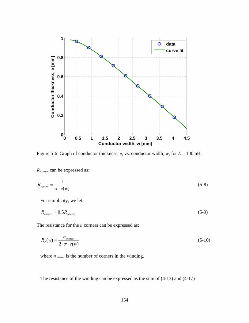
154
Rsquare can be expressed as:
)(1
weRsquare ⋅
=σ
(5-8)
For simplicity, we let
squarecorner RR 5.0= (5-9)
The resistance for the n corners can be expressed as:
)(2)(2 we
nwR corner
⋅⋅=
σ (5-10)
where ncorner is the number of corners in the winding.
The resistance of the winding can be expressed as the sum of (4-13) and (4-17)
Figure 5-6 Graph of conductor thickness, e, vs. conductor width, w, for L = 100 nH.
0 0.5 1 1.5 2 2.5 3 3.5 4 4.50
0.2
0.4
0.6
0.8
1
Conductor width, w [mm]
Con
duct
or th
ickn
ess,
e [m
m]
datacurve fit

155
)(2
)(
)(we
nwwl
wRcorner
⋅
+=
σ (5-11)
7. Plot R(w) vs. w and curve fit using 8th order polynomial
Resistance R is plotted as a function of conductor width, w, as shown in Fig. 5-7,
using (5-11). Equation (5-11) will result in a curve of the shape shown in Fig. 5-7, due to
a similar reason given in Chapter 4.8.
8. Obtain w at minimum point
The minimum point is found to be at w = 2.72 mm.
Figure 5-7 Graph of resistance, R, vs. conductor width, w.
0 1 2 3 4 52
3
4
5
6
7
8
9
10
11
Conductor width, w [mm]
Res
ista
nce,
R [m
Ω]
datacurve fit

156
9. Obtain corresponding e, g, l, R values
Conductor length, l(w), can be obtained from (5-1). Winding resistance, R(w), can be
obtained from (5-11). Conductor thickness e(w) can be obtained from (5-4) and (5-5).
Core thickness, g(e), can be obtained from (5-2). Table 5-2 tabulates the design values of
e, g, l, w and R for L0 = 100 nH.
Table 5-2 Inductor Design Values.
L [nH] e [mm] g [mm] l [mm] w [mm] R [ohm]
100 0.501 0.449 56.7 2.72 2.68
5.5 Effect of LTCC Inductor as Substrate
Using the inductor as the substrate helps in reducing the footprint of the circuitry,
since the surface real estate which was occupied by the bulky component is freed for
other devices and components. However, having a magnetic material below the circuitry
increases parasitic inductances in circuit traces and adversely affects circuit performance.
In this section, an LTCC inductor is fabricated and used as a substrate where its surface is
populated by the other devices and components of the circuit.
5.5.1 Inductor Substrate Fabrication Procedure
The inductor is designed to operate at a switching frequency 1.3 MHz, carrying a
nominal DC current of 16 A in a 5 V - to - 1.1 V buck converter. For this configuration,

157
the inductor is designed to have a value of 64 nH at full load. The inductor is designed
using the empirical model developed in Chapter 4.7. In this section, the fabrication
procedure of the inductor substrate is described. Fig. 5-8 shows the inductor substrate
fabrication procedure.
+ =
(a) Main bottom layer comprising 7 layers of ferrite tape, (b) main middle layer comprising 8 layers of ferrite tape, with C-shaped slot cut using laser, (c) laminate (a) with (b).
(a) (b) (c)
(d) (e) (f)
(d) Conductor paste dispensed into slot using a squeegee, with Kapton tape covering therest of the surface. Sample is heated to 70 °C to dry conductor paste. Procedure isrepeated 3 to 4 times until conductor paste fills slot completely. (e) After Kapton tape isremoved. (f) top main layer comprising 7 layers of ferrite tape.
(g) (h) (i)
(g) Stencil printed circuit layout on ferrite tape, (h) laminate (f) with (g) and cuttingthrough holes for inductor electrodes, (i) laminate (e) with (h), filling up holes with Ag/Ptpaste and laser cutting sample into desired size.
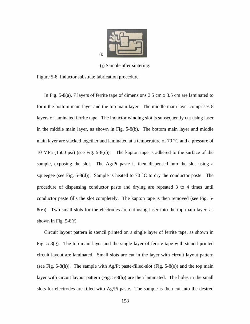
158
In Fig. 5-8(a), 7 layers of ferrite tape of dimensions 3.5 cm x 3.5 cm are laminated to
form the bottom main layer and the top main layer. The middle main layer comprises 8
layers of laminated ferrite tape. The inductor winding slot is subsequently cut using laser
in the middle main layer, as shown in Fig. 5-8(b). The bottom main layer and middle
main layer are stacked together and laminated at a temperature of 70 °C and a pressure of
10 MPa (1500 psi) (see Fig. 5-8(c)). The kapton tape is adhered to the surface of the
sample, exposing the slot. The Ag/Pt paste is then dispensed into the slot using a
squeegee (see Fig. 5-8(d)). Sample is heated to 70 °C to dry the conductor paste. The
procedure of dispensing conductor paste and drying are repeated 3 to 4 times until
conductor paste fills the slot completely. The kapton tape is then removed (see Fig. 5-
8(e)). Two small slots for the electrodes are cut using laser into the top main layer, as
shown in Fig. 5-8(f).
Circuit layout pattern is stencil printed on a single layer of ferrite tape, as shown in
Fig. 5-8(g). The top main layer and the single layer of ferrite tape with stencil printed
circuit layout are laminated. Small slots are cut in the layer with circuit layout pattern
(see Fig. 5-8(h)). The sample with Ag/Pt paste-filled-slot (Fig. 5-8(e)) and the top main
layer with circuit layout pattern (Fig. 5-8(h)) are then laminated. The holes in the small
slots for electrodes are filled with Ag/Pt paste. The sample is then cut into the desired
(j) Sample after sintering. Figure 5-8 Inductor substrate fabrication procedure.
(j)

159
size using laser (see Fig. 5-8(i)). The sample is then sintered using the sintering profile
shown in Fig. 2-21. Fig. 5-8(j) shows the sample after sintering.
5.5.2 Large Signal Measurement Results
The fabricated inductor is used as a substrate where other devices and components for
a buck converter are soldered on its surface. The circuit is operated as a 5 V – to – 1.1 V
buck converter at 2 MHz. Fig. 5-1 shows the circuit diagram of a Buck converter. Fig.
5-9 shows the photograph of the inductor substrate with surface mount devices to form a
single-phase buck converter. Table 5-3 tabulates the parts used in the fabrication of the
prototype.
Figure 5-10 shows that the gate voltage of the top and bottom MOSFETs of the buck
converter contains clear oscillations due to the presence of parasitic inductance. Due to
the presence of the magnetic substrate directly beneath the circuitry, parasitic inductances
of the traces become magnified. In Fig. 5-10 (a), it is evident that due to the trace
Figure 5-9 Buck converter on inductor substrate.
Qtop Qbot
Gate driver
Bootstrap diode, D1 Output capacitor, Co
Input capacitor, Cin
Bootstrap capacitor, C1
C2
Bottom MOSFET gate path
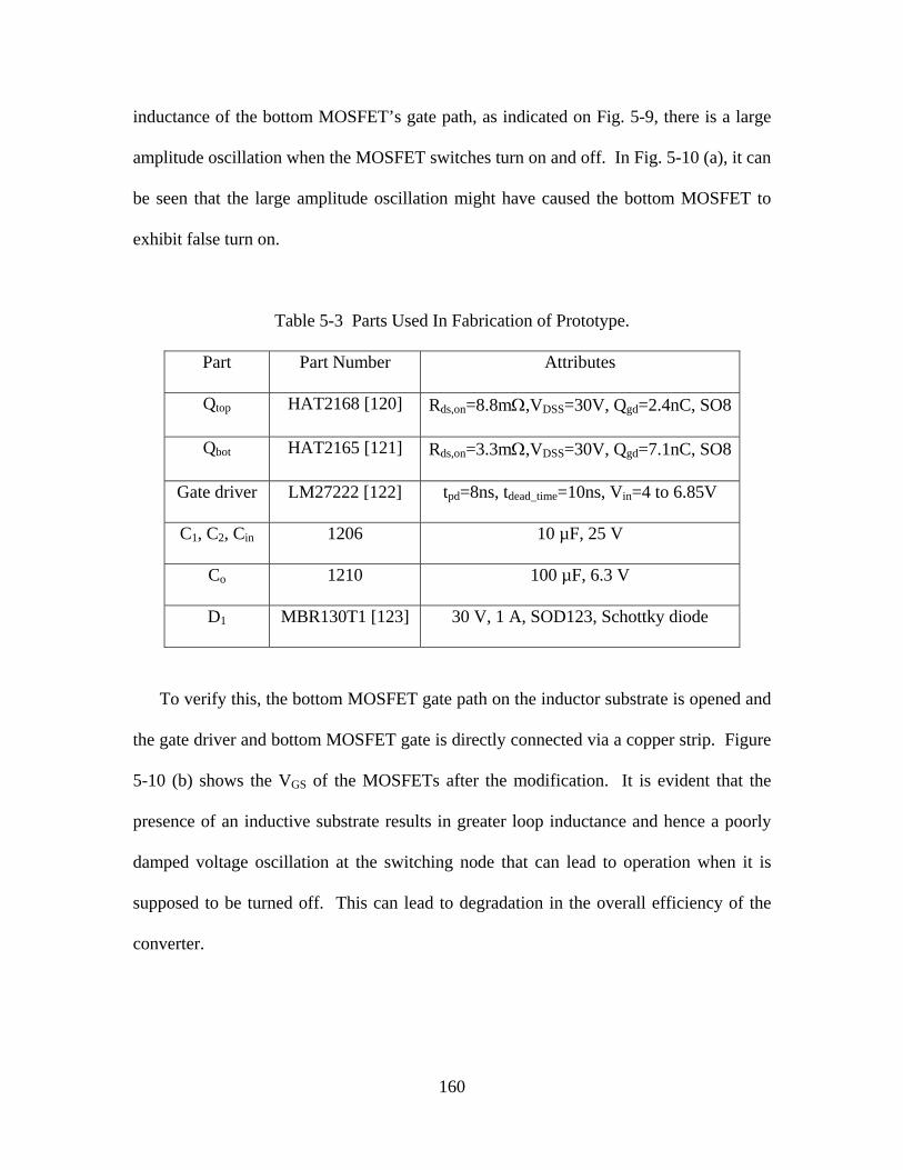
160
inductance of the bottom MOSFET’s gate path, as indicated on Fig. 5-9, there is a large
amplitude oscillation when the MOSFET switches turn on and off. In Fig. 5-10 (a), it can
be seen that the large amplitude oscillation might have caused the bottom MOSFET to
exhibit false turn on.
Table 5-3 Parts Used In Fabrication of Prototype.
Part Part Number Attributes
Qtop HAT2168 [120] Rds,on=8.8mΩ,VDSS=30V, Qgd=2.4nC, SO8
Qbot HAT2165 [121] Rds,on=3.3mΩ,VDSS=30V, Qgd=7.1nC, SO8
Gate driver LM27222 [122] tpd=8ns, tdead_time=10ns, Vin=4 to 6.85V
C1, C2, Cin 1206 10 µF, 25 V
Co 1210 100 µF, 6.3 V
D1 MBR130T1 [123] 30 V, 1 A, SOD123, Schottky diode
To verify this, the bottom MOSFET gate path on the inductor substrate is opened and
the gate driver and bottom MOSFET gate is directly connected via a copper strip. Figure
5-10 (b) shows the VGS of the MOSFETs after the modification. It is evident that the
presence of an inductive substrate results in greater loop inductance and hence a poorly
damped voltage oscillation at the switching node that can lead to operation when it is
supposed to be turned off. This can lead to degradation in the overall efficiency of the
converter.

161
5.6 Review of Electromagnetic Shielding Techniques
In monolithic radio frequency integrated circuit (RFIC) design, coupling noise from
inductors is reduced by using conductive guard rings surrounding the inductors [124,
125]. These guard rings serve as a shield to reduce the magnetic flux cross-talk coupling
from the inductor with other inductors and from affecting other circuitry. In high speed
digital signals, a meshed ground plane reduces degradation in signal rise time and voltage
Figure 5-10 VGS of the top and bottom MOSFETs (a) before (b) after connecting gate driver directly to the gate of the bottom MOSFET via copper strip.
Vgs_hiVgs_lo Vgs_hiVgs_lo
Vth = 1.67 V
(b)
Vgs_bot Vgs_top
Vth = 1.67 V
(a)
Vgs_top Vgs_bot

162
amplitude due to lower line capacitances. However, the longer current path in the case of
a meshed ground plane reduces propagation velocity due to increased line inductance
[126]. A floating shield technique is implemented to reduce passives loss on silicon
substrate for inductors in RFICs. In this case, the floating conductive shields link the
equal but opposing electric field from the passive component and its current return path,
keeping the floating shield at 0 V without an explicit ground reference [127]. In the
following section, we introduce the use of a shield between the magnetic component and
the rest of the circuit to mitigate the impact of the magnetic substrate on circuit loop
inductance.
5.7 LTCC Inductor Substrate with Conductive Shield
In the previous section, an inductor was fabricated using LTCC technology and used
as a substrate for the active circuitry by printing conductive traces on the inductor
magnetics and mounted devices on top. The performance of the system-on-inductor-
substrate was evaluated. The presence of a magnetic substrate below the circuitry created
additional parasitic inductances, which resulted in low-frequency oscillations and poor
overall efficiency. By introducing a conductive shield layer between the circuitry and
the inductor substrate, an attempt is made to alleviate the problem.
5.7.1 Simulation Study of Shielding for Magnetic Substrate
As observed in section 5.5, the presence of a magnetic substrate directly under the
circuitry traces can cause large amplitude and low frequency ringing, which can

163
adversely affect circuit performance. A conductive shield is introduced between the
magnetic substrate and the circuitry to alleviate the impact of the magnetic substrate on
circuit performance. In this section, comparison will be made between circuit operation
with and without shield. The effect of varying shield distance from circuit trace, shield
thickness and shield conductivity are studied.
5.7.1.1 Electromagnetic Influence of the Shield
In order to combat the negative effect of having a magnetic substrate below, the
inclusion of a conductive shield below the conductor traces is investigated. Fig. 5-11
shows the simulation structure with conductive shield between the conductive trace and
magnetic substrate. The trace is a copper sheet with dimensions of 11 mm x 12 mm with
thickness of 70 μm. There is a 1 mm x 5 mm slot in the trace. The dimensions were
chosen to be similar to that having two MOSFETs with SO8 packages placed side by
side, as shown in Fig. 5-9. The region in Fig. 5-11 is represented by the dotted lines in
Fig. 5-9. The magnetic substrate has dimensions of 28 mm x 28 mm x 1.2 mm. The
structure shown in Fig. 5-11 lies in the middle of the magnetic substrate. The thick arrow
in Fig. 5-11 indicates the direction of current flow in the trace. Figure 5-12 shows the 2-
D drawing of the section indicated by the dotted line in Fig. 5-11 for the various cases of
with or without shield and with or without inductor substrate. The relative permeability
of the magnetic substrate is 60. The conductivity of the shield and conductor is 1.7 × 10⁷
S/m. Simulation is performed for a current of 1 A passing through the conductor. The
frequency of the current in the simulation is 1.3 MHz.

164
Conductor Insulator
Magnetic Core
70 μmy
(b) Case B
(a) Case A
Conductor 70 μm
x
y
shield
trace
insulator
Magnetic substrate
Figure 5-11 Simulation structure with conductive shield between the conductive trace and magnetic substrate.
11 mm
12 mm
5 mm
5 mm
1 mm
Conductor Insulator
Magnetic Core
70 μmy
Shield x
(c) Case C

165
Figure 5-13 shows the comparison of normalized resistive loss for the four cases using
case A as the base for comparison. Fig. 5-14 shows the comparison of normalized loop
inductance for the four cases using case A as the base for comparison.
00.20.4
0.60.8
11.2
1.41.61.8
A B C DCases
Nor
mal
ized
loop
indu
ctan
ce
Figure 5-14 Normalized loop inductances for the four cases.
Figure 5-12 Cross-sectional drawings of simulation structures.
Conductor Insulator
70 μmy
Shield
x
(d) Case D
0
0.2
0.4
0.6
0.8
1
1.2
1.4
1.6
A B C DCases
Nor
mal
ized
pow
er lo
ss
Figure 5-13 Normalized power losses for the four cases.

166
5.7.1.2 Effect of Varying Shield Distance from Conductor
The insulator thickness, y, (see Fig. 5-11) is varied between 10μm to 200μm to study
its effect on loop inductance. Both the trace thickness and shield thickness are 70 μm.
The structure similar to that in Fig. 5-11 is simulated. Fig. 5-15 shows the graph of loop
inductance vs. insulator thickness. It is observed that as insulator thickness increases
from 10 μm to 200 μm, the loop inductance increases by almost 400 %. The increase in
loop inductance as insulator thickness increase is because the volume between the
conductor and the shield, which is available for energy storage increases. On the other
hand, the resistance decreases by less than 10 %. This is because as the distance between
the conductor and the shield increases, the coupling between the conductor and the shield
decreases. Hence, the current induced in the shield decreases, leading to lower I2R losses
in the shield. Therefore, to reduce trace inductance, the conductor has to be placed close
to the shield. From the point of view of reducing loop inductance, which is related to
power loss, it is consequently recommended to minimize insulator thickness. The price
for doing so is increased power loss in the shield.
5.7.1.3 Effect of Varying Shield Thickness
In this section the same structure in Fig. 5-11 is used. The shield thickness, x, is
varied between 5 μm to 200 μm to study its effect on loop inductance and power loss of
the system. The simulation is performed for a 1.3 MHz, 1 A current in the conductor.
Fig. 5-16 shows the graph of power loss and loop inductance vs. shield thickness for an
insulator thickness 50 µm and conductive trace thickness 70 µm.

167
It is observed from Fig. 5-16 that loop inductance is very high at low shield thickness,
which is attributed to the shield being ineffective at these thicknesses. The minimum
loop inductance occurs at a shield thickness of between 20 to 30 μm and increases
slightly as shield thickness increases. The power loss is low for thicker shield. It
increases rapidly as shield thickness decreases to below 50 μm. In view of this, it is more
0
0.5
1
1.5
0 50 100 150 200Insulator thickness [um]
Indu
ctan
ce [n
H]
0
1
2
3
Pow
er lo
ss [m
W]
Inductance
Pow er loss
Figure 5-15 Graph of power loss and inductance vs. insulator thickness. Both the conductor thickness and shield thicknesses are 70 μm.
Insulator thickness [μm]
0.4
0.6
0.8
1
0 50 100 150 200shield thickness [um]
Indu
ctan
ce [n
H]
0
5
10
15
Pow
er lo
ss [m
W]
InductancePow er loss
Figure 5-16 Graph of power loss and inductance vs. shield thickness. The conductor thickness is 70 μm and insulator thicknesses are 50 μm.
Shield thickness [μm]

168
feasible to have a shield thickness in the range of 50 μm to 100 μm, since both
inductance and power loss are low in this range. Thicker shields are not preferable since
increased shield thickness implies increased cost.
5.7.1.4 Effect of Varying Shield Conductivity
In this set of simulations, the structure in Fig. 5-11 is used. The shield thickness is 70
μm and the insulator thickness is 50 μm. The current in the conductor is 1 A at 1.3 MHz.
The shield conductivity is varied to observe its effect on loop inductance and power loss.
Fig. 5-17 shows the plot of inductance and power loss vs. shield conductivity.
When the conductivity is low, the energy stored in the system is high, which is a
result of the magnetic field from the current carrying conductor penetrating the shield and
entering the magnetic substrate. This manifests itself as parasitic inductance. When the
conductivity is high, the shield is effective in producing an opposing current flow as a
result of voltage induced in the shield, which prevents the magnetic field from entering
0
2
4
6
8
1.E+03 1.E+04 1.E+05 1.E+06 1.E+07 1.E+08Shield conductivity [S/m]
Indu
ctan
ce [n
H]
0
5
10
15
20
25
30
Pow
er lo
ss [m
W]
Pow er loss
Inductance
Figure 5-17 Graph of energy stored and power loss vs. shield conductivity. Conductorthickness and insulator thickness are both 50 μm. Shield thickness is 10 μm. Simulation frequency is 1.3 MHz.

169
the magnetic substrate. Thus, shield conductivity greater than 107 S/m is desirable since
the loop inductance and power loss are both low.
In summary, presence of magnetic substrate below a current conducting trace
increases the inductance of the trace which increases power loss. By introducing a shield
below the trace helps reduce the parasitic inductance of the trace as well as the overall
power loss. The trace inductance can be decreased by decreasing the distance between
the trace and the shield. Shield thickness in the range of 50 μm to 100 μm is
recommended as a compromise between parasitic inductance and power loss. Shield
conductivity greater than 107 S/m is desirable for the shield to be effective, for low
inductance as well as for low power loss.
5.7.2 Shielded Inductor Substrate Fabrication Procedure
To investigate the effect of metal shield between circuitry and magnetic substrate,
two samples were fabricated and tested. The first sample has no shield and the second
sample has a grounded shield under the MOSFETs. The shield thickness printed is
estimated to be around 50 μm, which is in the optimum range of thickness suggested in
section 5.7.1.3. From section 5.7.1.2, it was suggested that the thinner the insulator
(between the conductive trace and the shield), the lower the trace inductance. A single
layer of insulating LTCC tape is used as the insulator, which has a thickness of around 80
μm. The inductor substrate with integrated shield has dimensions 24mm x 24mm x
1.3mm. Fig. 5-18 shows the inductor fabrication procedure.
In the fabrication process of the trace and shield layer, low k dielectric LTCC tape
with part number ESL 41050 and Ag/Pt paste of part number 9516 are used. Both

170
materials are purchased from Electroscience Labs [28]. The metal trace from the gate
drive to the gate of the lower MOSFET is printed on the second layer and is directly
below the ground on the top layer. Fig. 5-19 shows the photograph of the trace layers
(first layer) for the two samples (a) with no shield and (b) with shield. The metal shield
is printed such that it is directly under the two MOSFETs. Since the MOSFETs carry
large current and are hard switched, the inductance in the input loop comprising the two
MOSFETs and the constant input voltage source resonates with the parasitic capacitances
across the MOSFETs, resulting in voltage ringing across the MOSFETs. Hence, to
reduce the parasitic inductance, a shield is introduced under the MOSFETs.
{d) {e) {f)
Figure 5-18 Fabrication procedure of inductor substrate. (a) Bottom main layercomprising 7 layers of ferrite tape, (b) Middle main layer comprising 8 layers of ferrite tape. An S-shape slot is cut using laser machining. (c) Top main layer comprising 7layers of ferrite tape. Two rectangular slots for inductor’s electrode cut using lasermachining, (d) Laminate (a) with (b), (e) Ag/Pt paste is dispensed into the slot asdescribed in Fig. 4-5. (f) Laminate (c) with (e), fill rectangular slots with Ag/Pt paste andsinter.
{a) {b) {c)

171
Figure 5-20 shows the improved buck converter with inclusion of metal shield above
magnetic substrate. The dotted line shows the position of the shield, which is below the
circuitry layer. The parts used in the fabrication of the prototypes are the same as that
tabulated in Table 5-3.
Figure 5-21 shows the waveforms at the switching point, Vsw, (see Fig. 5-1) of the
Buck converter (VDS of bottom switch) for sample (a) with no shield and (b) with shield
at no load. The circuit is tested at a switching frequency of 1.3 MHz. The input voltage
is 5 V and the output voltage is 1.1 V. The sample with no shield exhibit more severe
voltage oscillations compared to the sample with shield. The low frequency voltage
oscillations for the sample with no shield imply larger input loop inductance. The energy
stored in the parasitic loop inductance is dissipated in the loop [128]. Hence, the larger
the parasitic inductance, the larger the energy dissipated.
Figure 5-19 Trace layers for sample (a) with no shield and (b) with shield.
(a)
(b)
shield Circuit layout
First layer Second layer Third layer
First layer Second layer Third layer

172
Figure 5-21 Waveforms of VDS of bottom MOSFET in Buck converter for sample with (a) no shield and (b) with shield, at no load.
(a)
(b)
V [V]
t [ns] 0 400
0
0 5
5
Figure 5-20 Improved prototype Buck converter with inclusion of metal shield abovemagnetic substrate. The red dotted line shows the shape of the metal shield, which is below the circuitry.
Top switchBottom switch
Gate driver
Bootstrap diode Output capacitor
Input capacitor
Bootstrap capacitor
Shield
Inductor substrate
Decoupling capacitor

173
Figure 5-22 shows the power stage efficiency vs. Iout for the two samples with and
without shield. The power stage efficiency is obtained by the ratio of the DC output
power to DC input power. It is observed that the sample with no shield yields lower
efficiency than the one with shield.
In summary, an inductor fabricated using LTCC technology is used as a substrate
where the traces are printed and devices mounted on the surface. The presence of a
magnetic substrate below the circuitry creates additional parasitic inductances, which
results in large magnitude and low frequency oscillations. The effect of the presence of
a conductive shield helps to reduce trace inductance and improve circuit performance.
Appropriate shield conductivity is necessary to lower the trace inductance and minimize
power loss. Traces should be placed close to the shield to minimize inductance. Larger
power loss is incurred in the sample with no shield.
Figure 5-22 Power stage efficiency vs. output current for sample with shield and without shield, measured according to the methods of the circuits in Fig. 5-9.
70
75
80
85
90
0 2 4 6Output current [A]
Effi
cien
cy [%
]
Shield
No shield

174
5.8 Experimental Study of Substrate Structures
The popularity of portable devices makes size reduction of converters necessary to
decrease the dimensions of the overall system. In a dc-dc converter, the bulkiest
components are the capacitors and the inductors. Several companies that specialize in the
development of power ICs with inductors-in-package have expanded their portfolio into
buck regulators [129-132]. Several of these regulators make use of an inductor, which is
essentially a copper spiral sandwiched between two magnetic cores [133]. These
inductors are mostly co-packaged side-by-side with the buck converter semiconductor
devices, but this increases the footprint. Table 5-4 shows some of the commercial buck
regulators available on the market with integrated inductors and load currents in the
ampere range [133].
Using the inductor as the substrate carrying the semiconductor and the other
electronic components has been proposed as a means to reduce the overall footprint and
to increase the power density of the converter [134-137]. A low-profile LTCC inductor
substrate using NiCuZn ferrite material for micro dc-dc converters has been developed in
[138] and [139]. In 2007 and 2008, Fuji Electric Technology and National
Semiconductor released the FB6831J [140] and LM3218 [141] buck regulators
integrating the inductor as a substrate. Both products are targeted at applications with
current in the hundreds of mA range. An embedded inductor using spin-sprayed NiZn
ferrite film in polymer substrate has also been developed [142].

175
Table 5-4 Commercial Buck Regulators with Integrated Inductor and Load Currents in
The Ampere Range [133]
Model Input Voltage (V)
Output Voltage
(V)
Current (A)
Switching Frequency
(MHz) Inductor Package Size
(mm)
Enpirion EN5360D (2nd gen part) 2.375 to 5.5 0.8 to 3.3 6 5
Copper spiral on
ferrite
8.1 × 17 × 2.2, DFN48
Enpirion EN5336Q (2nd gen part) 2.375 to 5.5 0.8 to 3.3 3 5
Copper spiral on
ferrite
7.5 × 10 × 1.85, QFN44
Micrel SuperLNR MIC38300 3.0 to 5.5 as low as
1.0 3 Not specified
Not specified
4 × 6 × 0.9, 28-pin MLF
Linear Technology LTM4600 DC/DC
µModule
4.5 to 20 (or 28 V) 0.6 to 5 10 A cont.,
14 A peak 0.850, typ. at full load
Shielded low-profile
inductor
15 × 15 × 2.8, LGA
Linear Technology LTM4601/02/03 DC/DC
µModule
4.5 to 20 (or 28) 0.6 to 5
6 A or 12 A, parallel for higher
current
0.850, typ. at full load
Shielded low-profile
inductor
15 × 15 × 2.8, LGA
Linear Technology LTM4604 µModule 2.35 to 5.5 0.8 to 5 4 1.25
Shielded low-profile
inductor
15 × 9 × 2.3, LGA
National Semiconductor LM3218 (2008) 2.7 to 5.5 0.8 to 3.6 0.5 2 Substrate 3 x 2.5 x 1.2
Fuji Electric Technology FB6831J (2007) 2.7 to 5.5 Min 0.8 0.5 2.5 Substrate 2.95 x 2.4 x
1.0
As the conductive traces are placed in proximity to the magnetic substrate, however,
trace inductances increase, adversely affecting circuit operation especially at high
currents. To mitigate the effect of the presence of a magnetic substrate, a conductive
shield is introduced in section 5.7, which helps to reduce the overall trace inductance, in
turn reducing switching losses in the active devices.
It is of interest to compare the difference in performance between placing the inductor
side-by-side with the active circuit and using the inductor as a substrate to the active
circuitry. The trade offs in performance with form factor is an area which is not yet
explored. With the introduction of the shield, using a grounded shield and a floating

176
shield are compared to see the impact of grounding the shield. In addition, to observe the
impact of using inductor as a substrate in the absence of a shield, the performance of
samples with no shield using inductor as substrate and placing inductor side-by-side are
also compared. Table 5-5 tabulates the various cases under comparison.
Table 5-5 Comparison of Cases with Substrate Inductor and Co-packaged Inductor.
A. Inductor as substrate B. Inductor side-by-side with actives
1 Actives layer with grounded shield Actives layer with grounded shield
2 Actives layer with floating shield Actives layer with floating shield
3 Actives layer without shield Actives layer without shield
In the previous section, LTCC insulator material is used as the carrier for the active
devices. However, since the insulator material is currently not co-fireable with the LTCC
ferrite tape, it is necessary to fire them separately. The brittleness of the ceramic and the
thickness of the carrier with integrated shield and circuit layout being less than 150 μm
makes it difficult to handle. Hence, pyralux5 [143] is used as an alternative solution for
this comparison. The organic insulator has a thickness of 50 μm. The copper layers have
a thickness of 70 μm each. Fig. 5-23 (a) shows the 3-D view of surface mount devices
and components, with pyralux carrier and substrate inductor. Fig. 5-23 (b) shows the 2-D
lay-up diagram of pyralux carrier and substrate inductor.
5 Pyralux - organic insulator with copper sheets adhered to both sides

177
5.8.1 Samples Fabrication Procedure
The fabrication procedure of the inductor used for this set of experiments is the same
as that described in Fig. 5-18. The layer which contains the circuit layout where the
components and devices are soldered on is fabricated using pyralux [143], which is
essentially a layer of organic material sandwiched by copper sheets on both sides. The
pyralux has a layer of copper with thickness of 70 μm on both sides. The organic layer is
50 μm.
Figure 5-23 Surface mount devices and components, with pyralux carrier and substrate inductor. (a) 3-D view (b) 2-D lay-up diagram of pyralux carrier and substrate inductor.
1.2 mm 50 μm 70 μm
Copper traces Pyralux
Planar inductor (b)
28 mm
28 mm
50 μm
1.2 mm
19 mm
19 mm
Planar inductor
Pyralux
Copper traces
(a)
Surface mount devices and components

178
The starting material is a 28 mm x 28 mm pyralux. A piece of Kapton tape is pasted
on both sides of the pyralux. The circuit layout pattern is cut on the Kapton layer using
laser. The same is done for the rest of the circuitry on the reverse side. The Kapton layer
on top of the copper which is to be etched is peeled off using a tweezer. The sample is
then etched using ferric chloride solution. Fig. 5-24 (a) and (b) show the top layer and
reversed layer of pyralux for the samples with shield. Fig. 5-24 (c) and (d) show that for
the sample without shield.
Each pyralux actives carrier is tested using the LTCC inductor as a substrate and as a
co-packaged inductor. For the sample where the shield is grounded, a piece of copper
(a) (b)
Shield
(c)
L-shaped slot
(c) Top layer of pyralux showing circuit layout, (d) flipped layer of pyralux with part of circuit layout for sample without shield.
(d)
(a) Top layer of pyralux showing circuit layout, (b) flipped layer of pyralux showing shield and part of circuit layout for sample with shield.
Ground
Figure 5-24 Pyralux layer with circuit layout on top layer, with and without shield on flipped layer.
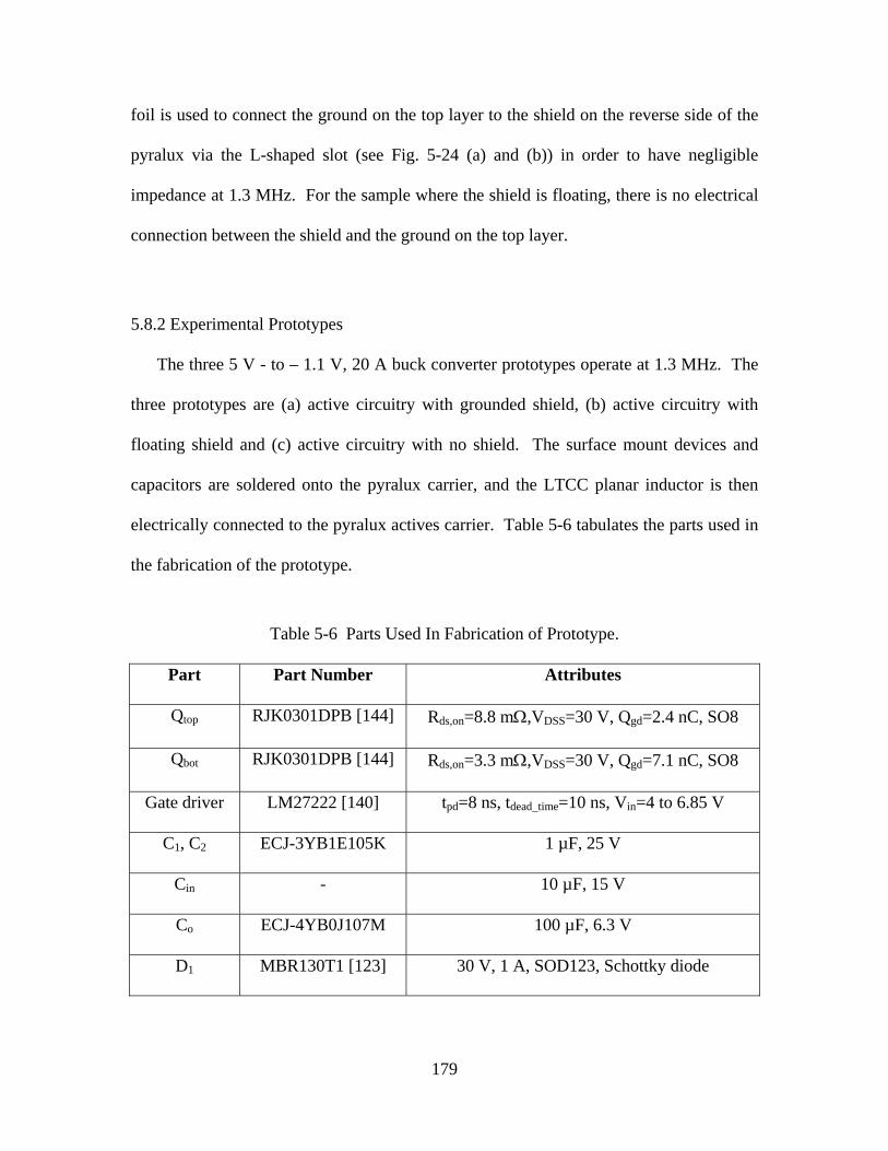
179
foil is used to connect the ground on the top layer to the shield on the reverse side of the
pyralux via the L-shaped slot (see Fig. 5-24 (a) and (b)) in order to have negligible
impedance at 1.3 MHz. For the sample where the shield is floating, there is no electrical
connection between the shield and the ground on the top layer.
5.8.2 Experimental Prototypes
The three 5 V - to – 1.1 V, 20 A buck converter prototypes operate at 1.3 MHz. The
three prototypes are (a) active circuitry with grounded shield, (b) active circuitry with
floating shield and (c) active circuitry with no shield. The surface mount devices and
capacitors are soldered onto the pyralux carrier, and the LTCC planar inductor is then
electrically connected to the pyralux actives carrier. Table 5-6 tabulates the parts used in
the fabrication of the prototype.
Table 5-6 Parts Used In Fabrication of Prototype.
Part Part Number Attributes
Qtop RJK0301DPB [144] Rds,on=8.8 mΩ,VDSS=30 V, Qgd=2.4 nC, SO8
Qbot RJK0301DPB [144] Rds,on=3.3 mΩ,VDSS=30 V, Qgd=7.1 nC, SO8
Gate driver LM27222 [140] tpd=8 ns, tdead_time=10 ns, Vin=4 to 6.85 V
C1, C2 ECJ-3YB1E105K 1 µF, 25 V
Cin - 10 µF, 15 V
Co ECJ-4YB0J107M 100 µF, 6.3 V
D1 MBR130T1 [123] 30 V, 1 A, SOD123, Schottky diode

180
When the inductor is used as a substrate, the pyralux layer with the active circuitry is
connected to the inductor by placing it on top of the inductor, as shown in Fig. 5-25 (a).
When the active circuitry is co-packaged with the inductor, the active circuitry is placed
by the side of the inductor, as shown in Fig. 5-25 (b).
The same inductor is used for all six test cases. Since the active circuitry is connected
to the inductor via thick copper straps for the cases using the co-packaged inductor, the
Decoupling capacitor
Output capacitor Input capacitor
Bottom switch
Top switch
Bootstrap capacitor
Inductor
Bootstrap diode Gate drive
(b)
Figure 5-25 Prototype buck converter with integrated shield and inductor (a) as substrate, (b) inductor placed on the side of active circuitry.
Inductor substrate
Bootstrap diode
Bootstrap capacitor
Gate drive
Output capacitorInput capacitor
Bottom switch
Top switch
Decoupling capacitor
(a)
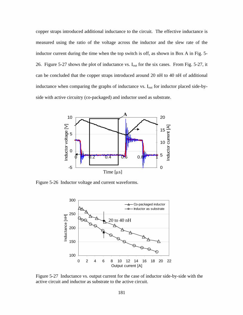
181
copper straps introduced additional inductance to the circuit. The effective inductance is
measured using the ratio of the voltage across the inductor and the slew rate of the
inductor current during the time when the top switch is off, as shown in Box A in Fig. 5-
26. Figure 5-27 shows the plot of inductance vs. Iout for the six cases. From Fig. 5-27, it
can be concluded that the copper straps introduced around 20 nH to 40 nH of additional
inductance when comparing the graphs of inductance vs. Iout for inductor placed side-by-
side with active circuitry (co-packaged) and inductor used as substrate.
100
150
200
250
300
0 2 4 6 8 10 12 14 16 18 20 22Output current [A]
Indu
ctan
ce [n
H]
Co-packaged inductorInductor as substrate
Figure 5-27 Inductance vs. output current for the case of inductor side-by-side with the active circuit and inductor as substrate to the active circuit.
20 to 40 nH
Figure 5-26 Inductor voltage and current waveforms.
-5
0
5
10
0 0.2 0.4 0.6 0.8 1
time [us]
Indu
ctor
vol
tage
[V]
0
5
10
15
20
Indu
ctor
cur
rent
[A]
A
Time [μs]

182
5.8.3 Metrics Comparison
The metrics used for comparison are percentage overshoot across the MOSFETs, the
ringing frequency, the switching loss, and the power stage efficiency. To obtain the
voltage overshoot and the switching loss, the voltage waveforms across the top and
bottom MOSFETs are obtained for the six cases. Figure 5-28 shows the voltage
waveforms across the top MOSFET and Fig. 5-29 shows that for the bottom MOSFET
for the six cases in Table 5-5.
t [ns] 0 4000 5
V [V]
t [ns]0 40005
V [V]
(c) Inductor as substrate with floating shield
(d) Inductor on the side with floating shield.
t [ns] 0 4000 5
(a) Inductor as substrate with grounded shield
(b) Inductor on the side with grounded shield
V [V]
t [ns] 0 40005
V [V]
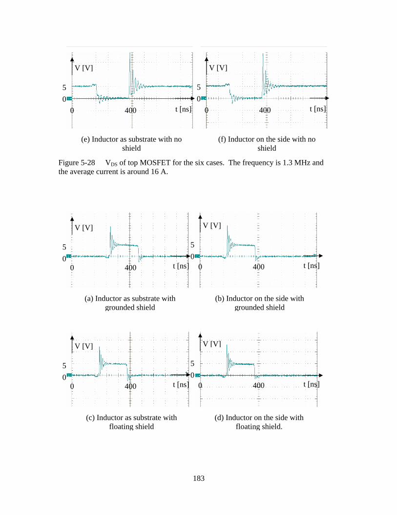
183
(c) Inductor as substrate with floating shield
(d) Inductor on the side with floating shield.
t [ns]0 4000 5
V [V]
t [ns]0 40005
V [V]
(a) Inductor as substrate with grounded shield
(b) Inductor on the side with grounded shield
t [ns]0 4000 5
V [V]
t [ns]0 40005
V [V]
t [ns] 0 4000 5
V [V]
t [ns]0 40005
V [V]
(f) Inductor on the side with no shield
(e) Inductor as substrate with no shield
Figure 5-28 VDS of top MOSFET for the six cases. The frequency is 1.3 MHz and the average current is around 16 A.

184
5.8.3.1. Voltage overshoot comparison
The impact of the presence of an inductive substrate and the effect of shielding can
manifest itself in the form of voltage overshoot. This will determine the voltage rating of
the devices required. Table 5-7 tabulates the voltage overshoot and normalized voltage
overshoot across the top and bottom MOSFETs for each of the six cases.
Table 5-7 Voltage Overshoot Comparison.
Sample Description Vtop Vbot Vtop,n Vbot,n
A1 Actives layer with grounded shield
with inductor as substrate 8.8 7.8 1.000 1.000
A2 Actives layer with grounded shield
using co-packaged inductor 7.9 8.2 0.898 1.051
B1 Actives layer with floating shield
with inductor as substrate 8 7.5 0.909 0.962
B2 Actives layer with floating shield
using co-packaged inductor 6.9 8 0.784 1.026
C1 Actives layer without shield with
inductor as substrate 15.2 7.8 1.727 1.000
C2 Actives layer without shield using
co-packaged inductor 13.7 7.8 1.557 1.000
(e) Inductor as substrate with no shield
(d) Inductor on the side with no shield
Figure 5-29 VDS of bottom MOSFET for the six cases. The frequency is 1.3 MHz and the average current is around 16 A.
t [ns]0 4000 5
V [V]
t [ns]0 40005
V [V]

185
The voltage overshoot observed in Fig. 5-28 is relatively high compared with that in
Fig. 5-21 because in Fig. 5-21, the waveforms are obtained at no load, whereas in Fig. 5-
28, the load current is 16 A.
From Table 5-7, the voltage overshoot across the top MOSFET is significantly
higher for the cases where there is no shield. MOSFET voltage rating greater than 20 V
is required for the top MOSFETs if no shield is used. For the cases with shield,
MOSFETs with voltage rating of 20 V would suffice for a load current of 16 A.
5.8.3.2. Parasitic inductance
The parasitic loop inductance in the input loop acts as an energy storage center and
this energy is dissipated in the loop via the trace resistances and resistances in the
switches. This power loss leads to degradation of performance of the circuit in the form
of decreased efficiency. The loop inductance can be calculated using
ossloopr
CLf
π21
= (5-12)
where fr is the frequency of oscillation of the voltage waveform of the MOSFET, Lloop is
the input loop inductance, and Coss is the output capacitance of the MOSFETs. fr is
calculated using the first three oscillations in the voltage across the top MOSFET. Coss is
taken to be 1450 pF from the datasheet [144]. The power dissipated is calculated using
221 2 ⋅⋅⋅= fiLP loop (5-13)
where Lloop is the loop inductance, f is the switching frequency, 1.3 MHz. The 2 at the
end of the equation represents turn on and turn off within a cycle. Table 5-8 tabulates the
loop inductance and power loss comparison at Iout = 16 A.
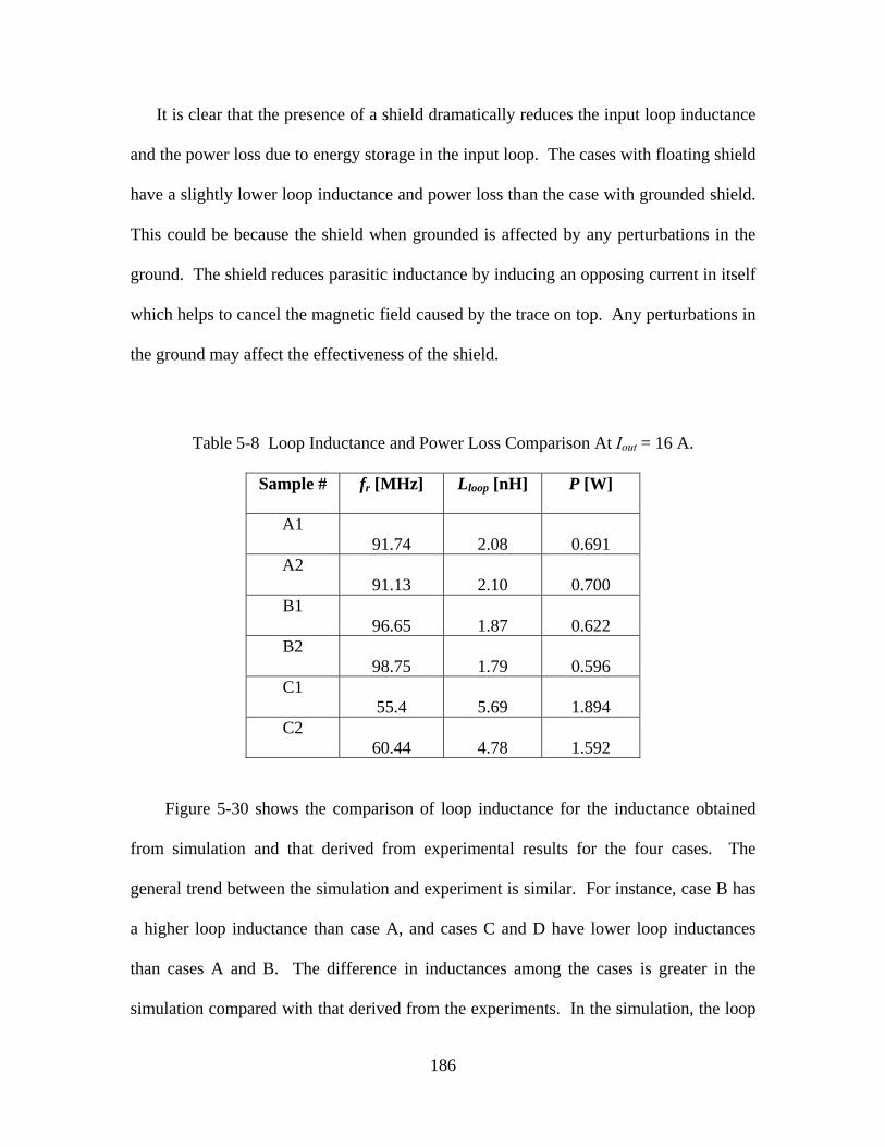
186
It is clear that the presence of a shield dramatically reduces the input loop inductance
and the power loss due to energy storage in the input loop. The cases with floating shield
have a slightly lower loop inductance and power loss than the case with grounded shield.
This could be because the shield when grounded is affected by any perturbations in the
ground. The shield reduces parasitic inductance by inducing an opposing current in itself
which helps to cancel the magnetic field caused by the trace on top. Any perturbations in
the ground may affect the effectiveness of the shield.
Table 5-8 Loop Inductance and Power Loss Comparison At Iout = 16 A.
Sample # fr [MHz] Lloop [nH] P [W]
A1 91.74 2.08 0.691
A2 91.13 2.10 0.700
B1 96.65 1.87 0.622
B2 98.75 1.79 0.596
C1 55.4 5.69 1.894
C2 60.44 4.78 1.592
Figure 5-30 shows the comparison of loop inductance for the inductance obtained
from simulation and that derived from experimental results for the four cases. The
general trend between the simulation and experiment is similar. For instance, case B has
a higher loop inductance than case A, and cases C and D have lower loop inductances
than cases A and B. The difference in inductances among the cases is greater in the
simulation compared with that derived from the experiments. In the simulation, the loop
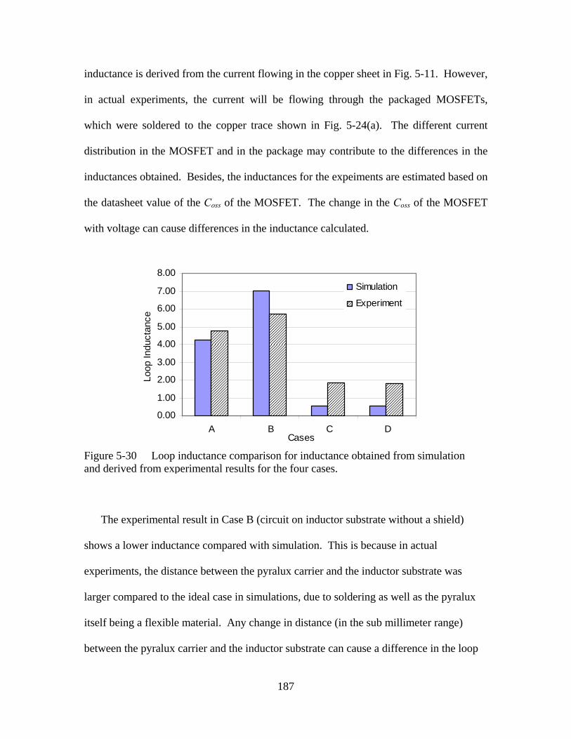
187
inductance is derived from the current flowing in the copper sheet in Fig. 5-11. However,
in actual experiments, the current will be flowing through the packaged MOSFETs,
which were soldered to the copper trace shown in Fig. 5-24(a). The different current
distribution in the MOSFET and in the package may contribute to the differences in the
inductances obtained. Besides, the inductances for the expeiments are estimated based on
the datasheet value of the Coss of the MOSFET. The change in the Coss of the MOSFET
with voltage can cause differences in the inductance calculated.
The experimental result in Case B (circuit on inductor substrate without a shield)
shows a lower inductance compared with simulation. This is because in actual
experiments, the distance between the pyralux carrier and the inductor substrate was
larger compared to the ideal case in simulations, due to soldering as well as the pyralux
itself being a flexible material. Any change in distance (in the sub millimeter range)
between the pyralux carrier and the inductor substrate can cause a difference in the loop
Figure 5-30 Loop inductance comparison for inductance obtained from simulation and derived from experimental results for the four cases.
0.00
1.00
2.00
3.00
4.00
5.00
6.00
7.00
8.00
A B C DCases
Loop
Indu
ctan
ce
Simulation
Experiment

188
inductance. As a result, the effect of the inductor substrate may not as pronounced in the
actual case due to the larger distance between the inductor substrate and the pyralux
carrier. In addition, any small difference in the placement of the input capacitor, as well
as the distance between the two MOSFETs can cause a difference in the physical loop
size, which will affect the loop inductance.
5.8.3.3 Efficiency
The power stage efficiency is compared for the six cases. Figure 5-31 (a) shows the
graph of efficiency vs. Iout. The efficiency curves are relatively close for the cases with
grounded and floating shield, using the substrate inductor or co-packaged inductor. The
efficiency is appreciably higher for the four cases with shield, both using substrate
inductor and co-packaged inductor, compared with the two cases with no shield. The
circuit with no shield on inductor substrate has the lowest efficiency. Its efficiency at 16
A is around 5-7 % lower than the cases with shield. The case of circuit with no shield co-
packaged with inductor is slightly lower than the cases with shield. The cases with
floating shield have slightly higher efficiency compared with the cases with grounded
shield. The possible reason was mentioned in the previous section. For the cases with
shield, the circuit with co-packaged inductor shows slightly higher efficiency than the
cases with inductor as substrate. This is due to the higher output inductance seen by the
circuit, which is due to the copper straps used for electrical connection.

189
5.8.3.4 Gate Drive Input Power
Table 5-9 tabulates the comparison of gate drive input power for the six cases. The
gate drive input power is the power input to the gate drive circuit, which is provided by
another power supply. The gate drive input power is significantly higher for the cases
with no shield. The case of the circuit with no shield on inductor substrate exhibits the
highest gate drive loss. The four cases with shield have similar gate drive loss.
From the experimental results, when the inductor is used as a substrate and in the
absence of a shield, the loop inductance is increased, leading to higher losses. Losses in
both the gate drive and the power stage are increased. Both power losses are shown to be
reduced by introducing a shield below the active circuitry. The losses are relatively close
when the inductor is used as a substrate or is co-packaged when there is a shield below
the circuit traces. The cases with floating shield show a slightly higher efficiency than
the cases with grounded shield.
Figure 5-31 Power stage efficiency vs. Iout for the six cases.
60
65
70
75
80
85
90
95
0 2 4 6 8 10 12 14 16 18 20 22Output current [A]
Effic
ienc
y [%
]
A1-circuit w gnded shd on L substrateA2-circuit w gnded shd w co-packaged LB1-circuit w /o shd on L substrateB2-circuit w /o shd w co-packaged LC1-circuit w f loating shd on L substrateC2-circuit w f loating shd w co-packaged L
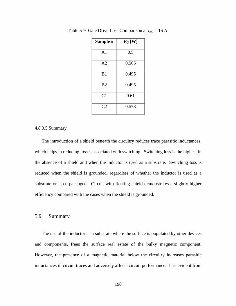
190
Table 5-9 Gate Drive Loss Comparison at Iout = 16 A.
Sample # PG [W]
A1 0.5
A2 0.505
B1 0.495
B2 0.495
C1 0.61
C2 0.573
4.8.3.5 Summary
The introduction of a shield beneath the circuitry reduces trace parasitic inductances,
which helps in reducing losses associated with switching. Switching loss is the highest in
the absence of a shield and when the inductor is used as a substrate. Switching loss is
reduced when the shield is grounded, regardless of whether the inductor is used as a
substrate or is co-packaged. Circuit with floating shield demonstrates a slightly higher
efficiency compared with the cases when the shield is grounded.
5.9 Summary
The use of the inductor as a substrate where the surface is populated by other devices
and components, frees the surface real estate of the bulky magnetic component.
However, the presence of a magnetic material below the circuitry increases parasitic
inductances in circuit traces and adversely affects circuit performance. It is evident from
191
experimental results that the presence of an inductive substrate results in greater loop
inductance and hence a poorly damped voltage oscillation across the devices, which can
lead to operation when it is supposed to be turned off. This can lead to degradation in the
overall efficiency of the converter. A conductive shield introduced between the magnetic
substrate and the circuitry helps alleviate the impact of the magnetic substrate on circuit
operation. Parasitic inductances, which cause voltage oscillations and overshoots across
devices reduces with proximity between the shield and the circuitry. The shield thickness
in the range of 50 μm to 100 μm is found to be a good compromise between power loss
and parasitic inductance reduction. The shield is effective when its conductivity is above
107 S/m. Experimental results show a reduction in voltage oscillation and overshoot
across the devices of the buck converter, reduction in input loop inductance, as well as an
increase in efficiency when a shield is incorporated. Gate drive loss can also be reduced
with the presence of a shield. Circuits with floating shields under it exhibit slightly better
efficiency compared with when the shield is grounded. When an inductor is to be used as
a substrate, a 5 % to 7 % improvement in efficiency can be obtained when a shield is
incorporated.

192
Chapter 6. Conclusion and Further Work
6.1 Conclusion
Using LTCC technology for power electronic applications is a new area. It has not
been thoroughly explored before, partly due to the limitations of the current LTCC
processing technology for high-current applications, as well as a widespread interest in
on-chip magnetics integration, which currently dominates low-power applications. The
use of low temperature co-fired ceramics (LTCC) technology for power converter
magnetics integration is developed to accommodate the requirement of fabricating
magnetic samples with thick conductors for power applications.
Prior to the use of the ceramic magnetic material for making the inductors, electrical
characterization is performed to understand the electrical behavior of the material and to
understand its suitable regions of operation. A power loss empirical model based on the
Steinmetz equation is developed to help in the estimation of losses at the targeted
frequency range of 1 MHz to 4 MHz, an operating temperature between 25 °C and 70 °C,
DC pre-magnetization from 0 A/m to 1780 A/m, and AC magnetic flux densities between
5 mT and 50 mT. Temperature and DC pre-magnetization dependence on Steinmetz
exponents are included in the model to more accurately describe the loss behavior.
Various geometries are evaluated in the development of LTCC technology to
fabricate chip inductors. An inductor with a short winding surrounded by magnetic
material is desirable due to the requirement to conduct large currents. Conductor
geometry is studied to select a suitable cross-sectional shape to obtain a smaller footprint
as well as lower losses, and the LTCC process is modified to produce conductors of the

193
desired rectangular cross-sectional shape, as well as to enable the fabrication of magnetic
components with thick conductors. Inductors with this geometry exhibit varying
inductance with current, which helps improve the converter efficiency at light load.
Parametric variation of the inductor geometry is performed in an effort to develop an
empirical model to describe the change in inductance with DC current.
Using the inductor as the substrate, where its surface can be populated by the
semiconductor and the other electronic components, is a next step to improving the power
density. The negative impact of the presence of a magnetic substrate in close proximity
to the circuitry can be mitigated by the introduction of a conductive shield between the
circuitry and the magnetic substrate. Parasitic inductance is found to decrease with the
decrease in distance between the shield and the circuitry. A shield thickness in the range
of 50 μm to 100 μm is found to be a good compromise between power loss and parasitic
inductance reduction. The effectiveness of the shield is apparent when its conductivity is
above 107 S/m.

194
6.2 Further Work
The use of LTCC ceramic magnetic material shows promise for magnetics integration
for power applications. In the materials and processing aspect, ferrite tapes of greater
thicknesses can be casted, as opposed to laminating many layers of the tape. Conductive
fillers like silver flakes or silver powder can be used for the conductor paste to improve
the conductivity. Other inductor geometries in the form of a perforated plate inductor can
be explored. The use of LTCC technology for making transformers for low-profile
power adapter applications can be an extension of the current work. In addition, the
extension of the work into the design and fabrication of coupled inductors for multi-phase
converters is also a possible area of research.

195
Appendix The parameters used in the equations below are with reference to Fig. A-1.
The magnetic flux density can be expressed as:
rNiBπμ2
= (A-1)
The magnetic flux density at the inner radius and outer radius can be expressed as:
ii r
NiBπμ2
= (A-2)
oo r
NiBπμ2
= (A-2)
The average magnetic flux can be obtained using the analysis below:
)( iom
r
rrrBdrBo
i
−=∫ (A-3)
Bi
Bo
Bm
ro ri r
B
Toroidal core
Cross-sectional view
h
Figure A-1 Illustrations for derivations. (a) Cross sectional drawing, (b) plan view drawing and (c) magnetic flux density illustration for toroidal core.
(a)
(b)
(c)

196
drr
NidrB o
i
o
i
r
r
r
r ∫∫ =πμ2
(A-4)
Equating (A-3) with (A-4),
The average magnetic flux, Bm, can be expressed as:
io
iom rr
rrr
NiB−−
⋅=)]ln()[ln(
2πμ
(A-5)
The specific power loss, using Steinmetz equation [79], can be expressed as:
βα BfKP pv ⋅⋅= (A-6)
Assuming frequency as a constant, the specific power loss can be expressed as:
βBPv ∝ (A-7)
The power loss in the core can be expressed as:
dVPP v∫= (A-8)
If magnetic flux density, B, is assumed to be a constant value of Bm, the power loss in the core,
P1, can be expressed as:
)( 21 hrdBP πβ∫∝
][ 221 io rrhBP −∝ πβ (A-9)
If magnetic flux density, B, is assumed to be not a constant, the power loss in the core, P2, can
be expressed as:
dVBP ∫∝ β2
)()2
( 22 hrd
rNiP ππμ β∫∝
][)2
(22 22
2βββ
πμ
βπ −− −−
∝ io rrnihP (A-10)

197
Reference
[1] R. Kraus, H. J. Mattausch, “Status and trends of power semiconductor device models for circuit simulation”, IEEE Trans. Power Electron., vol. 13, no. 3, pp. 452 – 465, May 1998.
[2] H. Ohashi, “Power electronics innovation with next generation advanced power devices”, in Proc. 25th Int. Telecommunications Energy Conf., Oct. 2003, pp. 9 – 13.
[3] J. D. van Wyk, F. C. Lee, Z. Liang, R. Chen, S. Wang, B. Lu, “Integrating active, passive and EMI-filter functions in power electronics systems: a case study of some technologies”, IEEE Trans. Power Electron., vol. 20, no. 3, pp. 523 – 536, May 2005.
[4] J.D. van Wyk, J.T. Strydom, L. Zhao, R. Chen, “Review of the development of high density integrated technology for electromagnetic power passives”, in Proc. IEEE 2nd Int. Conf. Integrated Power Systems, 2002, pp. 25-34.
[5] J. Ferrell, J. –S. Lai, T. Nergaard, X. Huang, L. Zhu, R. Davis, “The role of parasitic inductance in high-power planar transformer design and converter integration”, in Proc. Appl. Power Electron. Conf., 2004, vol. 1, pp. 510 – 515.
[6] Z. Liang, J. D. van Wyk, F. C. Lee, D. Boroyevich, “An integrated power switching stage with multichip planar interconnection construction”, in Proc. 4th Int. Power Electron. and Motion Control Conf., 2004, vol. 1, pp. 364 – 369.
[7] L. Li, P. Bowles, L. T. Hwang, S. Plager, “Embedded passives in organic substrate for bluetooth transceiver module”, in Proc. 53rd Electronic Components and Technology Conf., 27-30 May, 2003, pp. 464 - 469
[8] S. Stalf, “Printed inductors in RF consumer applications”, in Proc. Int. Conf. on Consumer Electronics., 19-21 June 2001 pp. 102 – 103.
[9] S. Dalmia, J. M. Hobbs, V. Sundaram, M. Swaminathan, Seock Hee Lee, F. Ayazi, G. White, S. Bhattacharya, “Design and optimization of high Q RF passives on SOP-based organic substrates”, in Proc. 52nd Electronic Components and Technology Conf., 28-31 May 2002, pp. 495 – 503.
[10] C. T. Chiu, C. L. Lin, T. S. Horng, S. M. Wu, C. P. Hung, “Design of Miniature Bandpass Filters Embedded in the Organic Substrate for RF SOP Applications”, in Proc. 36th European Microwave Conf., Sept. 2006 pp. 502 – 505.
[11] H. Tsujimoto, O. Ieyasu, ”High frequency transmission characteristic of co-planar film transformer fabricated on flexible polyamide film”, IEEE Trans. Magnetics., vol. 31, no. 6, part 2, Nov. 1995, pp. 4232 – 4234.
[12] X. Sun, D. Linten, O. Dupuis, G. Carchon, P. Soussan, S. Decoutere, W. De Raedt, “High-Q on-chip inductors using thin-film wafer level packaging technology demonstrated on a 90 nm RF-CMOS 5 GHz VCO”, in Proc. European Microwave Conf., vol. 1, 4-6 Oct. 2005.
[13] Chen Yang, Feng Liu, Tian-Ling Ren, Li-Tian Liu, Guang Chen, Xiao-Kang Guan, Wang, A., Hai-Gang Feng, “Ferrite-Integrated On-Chip Inductors for RF ICs”, IEEE Electron Dev. Lett., vol. 28, no. 7, pp. 652 – 655, July 2007.

198
[14] W. Bakalski, N. Ilkov, O. Dernovsek, R. Matz, W. Simburger, P. Weger, A. L. Scholtz, “5-6.5 GHz LTCC power amplifier module with 0.3 W at 2.4 V in Si-bipolar”, Electronics Lett., vol. 39, no. 4, pp. 375 – 376, 20 Feb 2003.
[15] D. Heo, A. Sutono, E. Chen, Y. Suh and J. Laskar, “A 1.9-GHz DECT CMOS Power Amplifier with Fully Integrated Multilayer LTCC Passives”, IEEE Microwave and Wireless Components Lett., vol. 11, no. 6, pp. 249 - 251, Jun 2001.
[16] M. Saidani, M. A. M. Gijs, “Hybrid flex foil-ferrite technology for miniaturized power and RF applications”, in Proc. IEEE Int. Symp. Industrial Electronics, vol. 1, 4-7 May 2004, pp. 23 - 26.
[17] T. Fujiwara, “Planar integrated magnetic component with transformer and inductor using multilayer printed wiring board”, IEEE Trans. Magnetics, vol. 34, no. 4, part 1, July 1998, pp. 2051 – 2053.
[18] E. Waffenschmidt, B. Ackermann J. A. Ferreira, ” Design method and material technologies for passives in printed circuit Board Embedded circuits”, IEEE Trans. Power Electron., vol. 20, no. 3, pp. 576 – 584, May 2005.
[19] M. Ludwig, M. Duffy, T. O'Donnell, P. McCloskey, P, S. C. O. Mathuna, “PCB integrated inductors for low power DC/DC converter”, IEEE Trans. Power Electron., vol. 18, no. 4, pp. 937 – 945, July 2003.
[20] M. Ludwig, M. Duffy, T. O'Donnell, P. McCloskey, P, S. C. O. Mathuna, “Design study for ultraflat PCB-integrated inductors for low-power conversion applications”, IEEE Trans. Magnetics, vol. 39, no. 5, part 2, pp. 3193 – 3195, Sept. 2003.
[21] R. Hahn, S. Krumbholz, H. Reichl, “Low profile power inductors based on ferromagnetic LTCC technology” in Proc. 56th Electronic Components and Technology Conf., 30 May-2 June 2006, pp. 528-533.
[22] P. Dhagat, Satish Prabhakaran, Charles R. Sullivan, “Comparison of magnetic materials for V-groove inductors in optimized high-frequency DC-DC converters”, IEEE Trans. Magnetics, vol. 40, no. 4, part 2, pp. 2008 – 2010, July. 2004.
[23] M. Rascon, R. Prieto, O. Garcia, J. A. Cobos, J. Uceda, “Design of very low profile magnetic components using flex foils”, IEEE 28th Appl. Power Electronics Conf., 23-27 Feb. 1997, vol. 2, pp. 561 – 567.
[24] Erik J. Brandon, Emily E. Wesseling, Vincent Chang, and William, B. Kuhn, “Printed microinductors on flexible substrates for power applications”, IEEE Trans. Compon., Packag. Manufact. Technol., vol. 26, no. 3, pp. 517-523, Sept. 2003.
[25] T. Mikura, K. Nakahara, K. Ikeda, K. Furukuwa, K. Onitsuka, “New substrate for micro DC-DC converter”, in Proc. 56th Electronic Components and Technology Conf., 30 May-2 June 2006, pp. 1326-1330.
[26] W. A. Roshen, R. L. Steigerwald, R. Charles, W. Earls, G. Claydon, C. F. Saj, “High efficiency, high density MHz magnetic components for a low profile converter”, IEEE Trans. Ind. Appl., vol. 31, no. 4, pp. 869 – 878, July-Aug. 1995.

199
[27] K. W. Moon, S. H. Hong, H. J. Kim, J. Kim, “A fabrication of DC-DC converter using LTCC NiZnCu ferrite thick film”, Digests IEEE Int. Magnetics Conf., 4-8 April 2005, pp. 1109 – 1110.
[28] Datasheets of LTCC tapes and conductior pastes of Electroscience Labs. [online] Available: http://www.electroscience.com
[29] Magali Brunet, Terence O’Donnell, Laurent Baud, Ningning Wang, Joe O’Brien, Paul McCloskey, and Sean C. O’Mathuna, “Electrical performance of Microtransformers for DC-DC converter applications”, IEEE Trans. Magnetics, vol. 38, no. 5, pp. 3174-3176, Sept. 2002.
[30] J. Y. Park, J. U. Bu, “Packaging compatible microtransformers on a silicon substrate”, IEEE Trans. Adv. Packag., vol. 26, no. 2, pp. 160 – 164, May 2003.
[31] M. Mino, T Yachi, A. Tago and K. Tanagisawa, “A new planar microtransformer for use in micro-switching-converters”, IEEE Trans. Magnetics, vol. 28, no. 4, pp. 1969-1973, July 1992.
[32] M. Mino, T. Yachi, A. Tago, K. Yanagisawa and K. Sakakibara, “Planar Microtranformer with monolithically-integrated rectifier diodes for micro-switching converters”, IEEE Trans.Magnetics, vol. 32, no. 2, pp. 291-296, Mar 1996.
[33] T. C. Neugebauer, D. J. Perreault, “Filters with inductance cancellation using printed circuit board transformers”, IEEE Trans. Power Electron., vol. 19, no. 3, pp. 591 – 602, May 2004.
[34] 1M. Joao Rosario, F. Le-Strat, P. –F. Alleaume, J. Caldinhas Vaz, J. Schroth, T. Muller, J. Costa Freire, “Low cost LTCC filters for a 30GHz satellite system”, in Proc. 33rd European Microwave Conf., 7-9 Oct. 2003, vol. 2, pp. 817 – 820.
[35] H. Khatri, L. E. Larson, D. Y. C. Lie, “On-chip monolithic filters for receiver interference suppression using bond-wire inductors”, Topical Meeting on Silicon Monolithic Integrated Circuits in RF Systems, 18-20 Jan. 2006, pp. 166-169. [36] Kai Zoschke, Klaus Buschick, Katrin Scherpinski, Thorsten Fischer, Jurgen Wolf, Oswin Ehrmann, Rafael Jordan, Herbert Reichl, Franz-Josef Schmuckle, “Stackable Thin Film Multi Layer Substrates with Integrated Passive Components”, in Proc. Electronic Components and Technology Conf., 30 May – 2 Jun 2006, pp. 806-813.
[37] C. Q. Scrantom, J. C. Lawson, “LTCC technology: where we are and where we're going. II”, IEEE MTT-S Symp. on Technologies for Wireless Applications, 21-24 Feb. 1999, pp. 193 – 200.
[38] Rao Tummala, “Fundamentals of Microsystems Packaging”, McGraw Hill Professional, 1st edition, May 2001.
[39] EPCOS. (2001, Jan.) Ferrite Polymer Composite (FPC) Film. [Online] Available: http://www.epcos.de/inf/80/ap/e0 001 000.htm
[40] Ning Zhu, “Planar Metallization Failure Modes in Integrated Power Electronics Modules”, Ph.D. dissertation, Virginia Tech.

200
[41] Wenduo Liu, “Alternative Structures for Integrated Electromagnetic Passives”, Ph.D. dissertation, Virginia Tech.
[42] M.A. Zampino, R. Kandukuri, W. K. Jones, “High performance thermal vias in LTCC substrates”, Eighth Intersociety Conf. on Thermal and Thermomechanical Phenomena in Electronic Systems, 2002, 30 May-1 June 2002, pp. 179 – 185.
[43] W.K. Jones, Yanqing Liu, Mingcong Gao, “Micro heat pipes in low temperature cofire ceramic (LTCC) substrates”, IEEE Transactions on Components and Packaging Technologies, vol. 26, no. 1, March 2003, pp. 110 – 115.
[44] L. Pergola, R. Gindera, D. Jager, R. Vahldieck, “An LTCC-Based Wireless Transceiver for Radio-Over-Fiber Applications”, IEEE Trans. Microwave Theory and Techniques, vol. 55, no. 3, March 2007, pp. 579 – 587.
[45] Jyh-Wen Sheen, “LTCC-MLC duplexer for DCS-1800”, IEEE Trans. Microwave Theory and Techniques, vol. 47, no. 9, part 2, Sept. 1999, pp. 1883 – 1890.
[46] I. Kowase, T. Sato, K. Yamasawa, Y. Miura, “A planar inductor using Mn-Zn ferrite/polyimide composite thick film for low-voltage, large-current DC-DC converter”, digests of the IEEE International Magnetics Conference, 4-8 April 2005, pp. 223 – 224.
[47] M. J. Prieto, A. M. Pernia, J. M. Lopera, J. A. Martin, F. Nuno, “Design and analysis of thick-film integrated inductors for power converters”, IEEE Trans. Ind. Appl., vol. 38, no. 2, pp. 543 – 552, March-April 2002.
[48] Jun Chul Kim, Dongsu Kim, Hyun Min Cho, Jong Chul Park, Nam Kee Kang, “A front end module and a filter using LTCC technology with heterogeneous dielectrics”, Ceramic Interconnect and Ceramic Microsystems Technology Conf., Apr. 2006, paper TP43, pp. 1-5.
[49] Leszek Golonka, Tomasz Zawada, Henryk Rogouszczak, Karol Malecha, Michal Chudy, Dorata Stadnik, Artur Dybko, “Three-dimensional fluidic microsystem fabricated in low temperature co-fire ceramic technology”, Ceramic Interconnect and Ceramic Microsystems Technology Conf., Apr. 2006, paper WA21, pp. 1-6.
[50] J. M. English and M. G. Allen, “Wireless micromachined ceramic pressure sensors”, in Proc. 12th IEEE Int. Conf. Micro Electro Mechanical Systems, 1999, pp. 511-516.
[51] Feng Zheng, Hubert George, and W. Kinzy Jones, “Development of a multi-channel electron multiplier using LTCC/thick silver cofired structures”, Ceramic Interconnect and Ceramic Microsystems Technology Conf., Apr. 2006, paper WA21, pp. 1-6.
[52] K. Itoh, et al., “Integrated even harmonic type direct conversion receiver for WCDMA mobile terminals (invited paper)”, Proc. Of 2002 RFIC Symp., pp 263-266.
[53] L. Larson and D. Jessie, “Packaging designs for radio-frequency ICs”, EE Times, Sept. 2003.
[54] New Jersey Nanotechnology Consortium [online] Available: http://www.njnano.org
[55] Wenxia Li and John J. Lannutti, “Curvature evolution in LTCC tapes and laminates”, IEEE Trans. Components and Packaging Technologies, vol. 28, no. 1, pp. 149-156, Mar 2005.

201
[56] T. Cheng and R. Raj, “Flaw generation during constrained sintering of metal-ceramic and metal-glass multilayer films”, J. Amer. Ceram. Soc., vol. 72, no. 9, pp. 1649 – 1655, 1989.
[57] C. H. Hsueh and A. G. Evans, “ Residual stress and cracking in metal/ceramic systems for microelectronics packaging’, J. Amer. Ceram. Soc., vol. 68, no. 3, pp. 120-127, 1985.
[58] J.-H. Jean and C.-R. Chang, “Camber development during cofiring Ag-based low dielectric-constant ceramic package”, J. Mater. Res., vol. 12, no. 10, pp. 2743-2750, 1997.
[59] B. Geller, B. Thaler, A. Fathy, M. J. Liberatore, H. D. Chen, G. Ayers, V. Pendrick, and Y. Narayan, “LTCC-M: a enabling technology for high performance multilayer RF systems”, Microwave J., vol. 42, no. 7, pp. 64-72, 1999.
[60] G.-Q. Lu, R. C. Sutterlin, and T. K. Gupta, “Effect of mismatched sintering kinetics on camber in a low-temperature cofired ceramic package”, J. Amer. Ceram. Soc., vol. 76, no. 8, pp. 1907-1914, 1993.
[61] S. –H. Lee, G. L. Messing, E. R. Twiname, A. Mohanram, C. A. Randall, and D. J. Green, “Co-sintering of multilayer ceramics”, Key Eng. Mater., vol. 206-213, p. 257-260, 2002.
[62] Datasheet for ESL 40010 [online]. Available: http://www.electroscience.com
[63] R. E. Mistler and E. R. Twiname, “Tape casting theory and practice”, Westerville, OH: Amer. Cer. Soc., 2000.
[64] http://www.accumet.com/
[65] Datasheet for ESL 2312, [online]. Available: http://www.electroscience.com
[66] Datasheet for ESL 953, [online]. Available: http://www.electroscience.com
[67] Bosui Liu; Xun Gong; Chappell, W.J.;, “Layer-by-layer polymer stereolithography fabrication for three-dimensional RF components”, IEEE Int. Microwave Symposium Digest, vol. 2, 6-11 June 2004, pp. 481 – 484.
[68] B. W. Hakki and P. D. Coleman, “A dielectric resonator method of measuring inductive capacities in the millimeter range,” IEEE Trans. Microwave Theory Tech., vol. MTT-8, pp. 402-410, July 1960.
[69] Hirofumi Kakemoto, Song-Min Nam, Satoshi Wada and Takaaki Tsurumi, “High-Frequency Dielectric Measurement Using Non-contact Probe for Dielectric Materials”, Jpn. J. Appl. Phys. 45 (2006) pp. 3002-3006.
[70] David V. Blackham, and Roger D. Pollard, “An Improved Technique for Permittivity Measurements Using a Coaxial Probe”, IEEE Trans. Instrumentation and Measurement, vol. 46, no. 5, oct. 1997, pp. 1093 – 1099.
[71] Yan Ye, Taijun Liu, Xingbin Zeng, Jiaming He, and Cevdet Akyel, “Accurate Permittivity Measurement Using the Cavity Perturbation Technique at ISM 5.8GHz Radio Band”, Int. Conf. Microwave and Millimeter Wave Technology, 18-21 April 2007 pp. 1 - 4.

202
[72] R. Linkous, A. W. Kelley, K. C. Armstrong, “An improved calorimeter for measuring the core loss of magnetic materials”, in proc. Appl. Power Electron. Conf., vol. 2, 6-10 Feb. 2000, pp. 633 – 639.
[73] D. Zhang, S. Birlasekaran, T. T. Sim, P. C. Hum Peng, “Ferrite core loss measurement with arbitrary wave excitation”, Int. Conf. on Power System Technology, 2004, vol. 1, 21-24 Nov. 2004, pp. 564 – 567.
[74] J. Zhang, G. Skutt, F. C. Lee, “Some practical issues related to core loss measurement using impedance analyzer approach”, in proc. Appl. Power Electron. Conf., vol. 2, no. 0, part 2, 5-9 March 1995, pp. 547 – 553.
[75] P.M. Gradzki and F.C. Lee, "High-Frequency Core Loss Characterization Technique Based on Impedance Measurement," in proc. High Frequency Power Conversion Conference, 1991, pp. 108-115.
[76] CECC 25 300. Magnetic oxide cores for power application. Harmonized system of quality assessment for electronic components, sectional specification, 1981.
[77] V. J. Thottuvelil, T. G. Wilson, Jr. H. A. Owen, “High-frequency measurement techniques for magnetic cores”, IEEE Trans. Power Electron., vol. 5, no. 1, Jan. 1990, pp. 41 – 53.
[78] H. Y. Chung, F. N. K. Poon, C. P. Liu, M. H. Pong, “Analysis of buck-boost converter inductor loss using a simple online B-H curve tracer”, in proc. Appl. Power Electron. Conf., 6-10 Feb. 2000, vol. 2, pp. 640 – 646.
[79] S. Mulder, Loss Formulas for Power Ferrites and their Use in Transformer Design. Eindhoven, The Netherlands: Philips, 1994.
[80] http://www.ferroxcube.com
[81] R. W. Erickson and D. Maksimovic, “Fundamentals of Power Electronics”, 2nd Edition, Springer, Jan 2001.
[82] W. J. Sarjeant, D. T. Staffiere, “A report on capacitors”, in proc. Appl. Power Electron. Conf., 3-7 March 1996, vol. 1, pp. 12 – 17.
[83] http://www.arrl.org - Hands-on Radio, Experiment #63 – About Capacitors
[84] W. Liu, “Alternative Structures for Integrated Electromagnetic Passives”, Ph. D. dissertation, Virginia Tech.
[85] “The Effect of Probe Input Capacitance on Measurement Accuracy” Tektronix Technical Brief.
[86] Instructions for Tektronix P5050, 10X, passive probe, 18 Oct 2001.
[87] Instructions for Tektronix P6243, 1 GHz, 10X, active probe instructions.
[88] Wolfgang Maichen, “Digital Timing Measurements, From Scopes and Probes to Timing and Jitter Series: Frontiers in Electronic Testing”, vol. 33, 2006.
[89] D. C. Jiles and D. L. Atherton, “Theory of ferromagnetic hysteresis,” J. Magnetism Magn. Mater., vol. 61, pp. 48–60, 1986.

203
[90] B. D. Coleman and M. L. Hodgdon, “A constitutive relation for rate independent hysteresis on ferromagnetically soft materials,” Int. J. Eng. Sci., vol. 24, no. 6, pp. 897–917, 1986.
[91] F. Preisach, “Über die magnetische nachwirkung,” Zeitschrift Phys., pp. 277–302, 1935.
[92] D. C. Jiles, “Frequency dependence of hysteresis curves in ‘nonconducting’ magnetic materials,” IEEE Trans. Magn., vol. 29, pp. 3490–3492, Nov. 1993.
[93] Kenneth H. Carpenter, “Simple Models for Dynamic Hysteresis Which Add Frequency-Dependent Losses to Static Models”, IEEE Trans. Magn., vol. 34, no. 3, pp. 619–622, May. 1998.
[94] Peter R. Wilson, J. Neil Ross, and Andrew D. Brown, “Modeling Frequency-Dependent Losses in Ferrite Cores”, IEEE Trans. Magn., vol. 40, no. 3, pp. 1537–1541, May. 2004.
[95] M. L. Hodgdon, “Applications of a theory of magnetic hysteresis,” IEEE Trans. Magn., vol. 24, pp. 218–221, Jan. 1988.
[96] I. D. Mayergoyz, “Dynamic Preisach models of hysteresis,” IEEE Trans. Magn., vol. 24, pp. 2925–2927, Sept. 1988.
[97] G. Bertotti, “Dynamic generalization of the scalar Preisach model of hysteresis,” IEEE Trans. Magn., vol. 28, pp. 2599–2601, Sept. 1992.
[98] A. Brockmeyer, “Experimental evaluation of the influence of DC-premagnetization on the properties of power electronic ferrites”, in proc. Appl. Power Electron. Conf., vol. 1, 3-7 March 1996, pp. 454 – 460.
[99] H. Y. Chung, F. N. K. Poon, C. P. Liu, M. H. Pong, “Analysis of buck-boost converter inductor loss using a simple online B-H curve tracer”, in proc. Appl. Power Electron. Conf., 6-10 Feb. 2000, vol. 2, pp. 640 – 646.
[100] J. Reinert, A. Brockmeyer, R. W. A. A. De Doncker, “Calculation of Losses in Ferro- and Ferrimagnetic Materials Based on the Modified Steinmetz Equation”, IEEE Trans. Industry Appl., vol. 37, no. 4, Jul/Aug 2001, pp. 1055-1061.
[101] W. Ruythooren, E. Beyne, J.-P Celis and J. De Boeck, “Integrated High-frequency inductors using amorphous electrodeposited Co-P Core”, IEEE Trans. Mag., 38(5), sept ’02, pg 3498.
[102] Srinivasan Iyengar, Trifon M. Liakopoulos and Chong H. Ahn, “A DC/DC Boost Converter Toward Fully On-Chip Integration Using New Micromachined Planar Inductors”, Proc. IEEE Power Electronics Specialists Conference, vol. 1, pp. 72-76, April 1999.
[103] H. Kurata, K. Shirakawa, O. Nakazima, K. Murakami, “Study of thin film micro transformer with high operating frequency and coupling coefficient”, IEEE Trans. Mag, 29(6), nov ’93, pp. 3204.

204
[104] Ahn, C.H.; Kim, Y.J.; Allen, M.G.; , ” A fully integrated planar toroidal inductor with a micromachined nickel-iron magnetic bar”, IEEE Trans. Component Packaging and Manufacturing Tech., vol. 17, no. 3, pp. 463-469, Sept. 1994.
[105] Charles R. Sullivan and Seth R. Sanders, “Design of microfabricated transformers and inductors for high-frequency power conversion”, IEEE Trans. Power Electron., vol. 11, no. 2, Mar ’96, pp. 228.
[106] H. Feng, G. Jelodin, K. Gong, R. Zhan, Q. Wu, C. Chen and A. Wang, “Super compact RFIC inductors in 0.18μm CMOS with copper interconnects”, IEEE Radio Frequency Integrated Circuits Symposium, 2002, pp. 443.
[107] Eberhard Waffenschmidt, J.A. Ferreira, “Embedded passives integrated circuits for power converters”, in proc. Power Electron. Specialists Conf. , 2002, pp. 12.
[108] Chong H. Ahn and Mark G. Allen, “A Planar micromachined spiral inductor for integrated magnetic microactuator applications”, J Micromech. Microeng. 3, 1993, pp. 37-44.
[109] M. Yamaguchi, K. Ishihara and K. I. Arai, “Application of Thin-film inductors to LC filters”, IEEE Trans. Mag., 29(6), nov ’93, pp. 3222.
[110] Musunuri, S.; Chapman, P.L.; Jun Zou; Chang Liu, “Design issues for monolithic DC-DC converters”, IEEE Trans. Power Electron., vol. 20, no. 3, pp. 639 – 649, May 2005.
[111] Hiroaki Tsujimoto and Ieyasu O, “High Frequency Transmission Characteristic of Co-planar Film Transformer Fabricated on Flexible Polyamide Film”, IEEE Trans. Mag., 31(6), Nov. 95, pp. 4232.
[112] Gustavo J. Mehas, Kip D. Coonley, Charles R. Sullivan, “Design of microfabricated inductors for microprocessor power delivery”, in proc. Appl. Power Electron. Conf., Mar. 1999, pp. 1181-1187.
[113] Julu Sun, Yuancheng Ren, Ming Xu and Fred C. Lee, “Light Load Efficiency Improvement for Laptop VRs”, in proc. Appl. Power Electron. Conf., Feb. 25 2007-March 1 2007, pp. 120 – 126. [114] R. W. Erickson, D. Maksimovic, “Fundamentals of Power Electronics, 2nd Edition, 2001, Kluwer Academic Publishers.
[115] L. Chai, C. Lopez, A. Shaikh, “Fine Line Printing Technologies for Microwave and Millimeter Wave Applications”, 36th International Symposium on Microelectronic proceedings, 2003, pp. ??.
[116] Katsuhiko Naka, “Using LFC Technology, Murata Makes Automotive Ceramic Substrates”, Asia Electronics Industry, vol. 10, serial number 103, April 2005, pp. 50-52.
[117] Jerzy A. Owczarek and Frank L. Howland, “A Study of the Off-Contact Screen Printing Process- Part I: Mode of the Printing Process and Some Results Derived From Experiments”, IEEE Trans. Components, Hybrids, and Manufacturing Tech., vol. 13. no. 2, June 1990, pp. 358-367.

205
[118] Jerzy A. Owczarek and Frank L. Howland, “A Study of the Off-Contact Screen Printing Process- Part II: Analysis of the Model of the Printing Process”, IEEE Trans. Components, Hybrids, and Manufacturing Tech., vol. 13. no. 2, June 1990, pp. 368-375.
[119] http://www.renesas.com
[120] Renesas HAT2168H, silicon N channel power MOS FET, Rev. 7.00, 20 Sept 2005
[121] Renesas HAT2165H, silicon N channel power MOS FET, Rev. 6.00, 20 Sept 2005
[122] National Semiconductor Corporation, LM27222, High-speed 4.5 A Synchronous MOSFET Driver, Sept. 2004. Website: http://www.national.com.
[123] Surface Mount Schottky Power Rectifier, MBR130T1/D, Jul 2005, Rev. 2. Website: http://onsemi.com.
[124] Pun, A.L.L.; Yeung, T.; Lau, J.; Clement, J.R.; Su, D.K.; “Substrate noise coupling through planar spiral inductor”, J. Solid-State Circuits, vol. 33, no. 6, Jun 1998, pp.877 – 884.
[125] Cheon Soo Kim, Piljae Park, Joung-Woo Park, Nam Hwang, Hyu Kyu Yu, “Deep trench guard technology to suppress coupling between inductors in silicon RF ICs”, IEEE Microwave Symp. Digest, vol. 3, 20 - 25 May 2001, pp. 1873 – 1876.
[126] Chung-Ping Chien, A. F. Burnett, J. M. Cech, M. H. Tanielian, “The signal transmission characteristics of embedded microstrip transmission lines over a meshed ground plane in copper/polyimide multichip module”, IEEE Trans. Components and Packaging Technologies, vol. 17, no. 4, Nov. 1994, pp. 578 – 583.
[127] T.S.D. Cheung, J. R. Long, “Shielded passive devices for silicon-based monolithic microwave and millimeter-wave integrated circuits” J. Solid State Circuits, vol. 41, no. 5, May 2006, pp. 1183 – 1200.
[128] Y. Ren, M. Xu, J. Zhou, Lee F. C., “Analytical loss model of power MOSFET”, IEEE Trans. Pow. Electron. vol. 21, no. 2, pp. 310, Mar 2006.
[129] Datasheets of products of Enpirion, Inc. [online]. Available: http://www.enpirion.com
[130] Datasheets of products of Micrel, Inc. [online]. Available: http://www.micrel.com
[131] Datasheets of products of Fuji Electric, Inc. [online]. Available: http://www.fujielectric.co.jp
[132] Datasheets of products of Linear Technology, Inc. Available: http://www.linear.com
[133] David Morrison, “Regulators Embed Inductors to Save Space and Ease Use”, Power Electronics Technology, July 2007, pp. 46-48.
[134] Y. Katayama, M. Edo, T. Denta , T. Kawashima, T. Ninomiya, “Optimum design method of CMOS IC for DC-DC converter that integrates power stage MOSFETs”, in Proc. Power Electronics Specialists Conf., vol. 6, 20-25 June 2004, pp. 4486 – 4491.
206
[135] Y. Katayama, S. Sugahara, H. Nakazawa, M. Edo, “High-power-density MHz-switching monolithic DC-DC converter with thin-film inductor”, in Proc. Power Electronics Specialists Conf., vol. 3, 18-23 June 2000, pp. 1485 – 1490.
[136] W. G. Hurley, M. C. Duffy, S. O'Reilly, S. C. O'Mathuna, “Impedance formulas for planar magnetic structures with spiral windings”, IEEE Trans. Industrial Electronics, vol. 46, no. 2, April 1999, pp. 271 – 278.
[137] J. M. Lopera, M. J. Prieto, A. M. Pernia, F. Nuno, M. J. M. De Graaf, J. W. Waanders, L. A. Barcia, “Design of integrated magnetic elements using thick-film technology”, IEEE Trans. Power Electronics, vol. 14, no. 3, May 1999, pp. 408 - 414
[138] R. Hahn, S. Krumbholz, H. Reichl, “Low profile power inductors based on ferromagnetic LTCC technology”, in Proc. 56th Electronic Components and Technology Conf., 30 May-2 June 2006, pp. 528-533.
[139] T. Mikura, K. Nakahara, K. Ikeda, K. Furukuwa, K. Onitsuka, “New substrate for micro DC-DC converter”, in Proc. 56th Electronic Components and Technology Conf., 30 May-2 June 2006, pp. 1326-1330.
[140] Fuji Power Supply Control IC, Micro DC-DC Converter, FB 6831 Application Note, Rev. 0, July 2006, Fuji Electric Device Technology, Co., Ltd. Website: http://www.fujielectric.com
[141] National Semiconductor Corporation, LM3218 650 mA Miniature, Adjustable, Step-Down DC-DC Converter for RF Power Amplifiers, 18 Mar 2008, Website: http://www.national.com
[142] S. Bae, H. –M. Jung, J. –S. Moon, Y. Mano, “Embedded inductor using Ni-Zn ferrite film in polymer substrate”, in Proc. IEEE Int. Magnetics Conf., 4-8 April 2005, pp. 1767 – 1768.
[143] Datasheets of products of Dupont, Inc. Available: http://www2.dupont.com/Pyralux/en_US
[144] Renesas RJK0301DPB, silicon N channel power MOS FET, Rev. 9.00, 19 Apr 2006.