overview of low temperature co-fired ceramics tape
TRANSCRIPT
Overview of low temperature co-®red ceramics tape technology formeso-system technology (MsST)
M.R. Gongora-Rubioa, P. Espinoza-Vallejosb, L. Sola-Lagunac, J.J. Santiago-AvileÂsb,*
aIPT, Av. Prof. Almeida Proda 532 C. Universitoria CEP 05508, SaÄo Paulo, BrazilbDepartment Electrical Engineering, University of Pennsylvania, 200 South 33rd St., Philadephia, PA 19104 6314, USA
cDuPont Electronic Material, Inc, Hwy 686, KM 2.3, Manati PR 00717, USA
Received 21 January 2000; received in revised form 18 October 2000; accepted 27 October 2000
Abstract
For certain applications low temperature co-®red ceramic (LTCC) tape materials used in multi-layer packages offers the potential of
emulating a great deal of silicon sensor/actuator technology at the meso scale level. The goal of this review is to describe meso-system
technology (MsST) using LTCC, thick ®lm and silicon technologies.
A mayor MST application being addressed today is ¯uid handling for miniaturized chemical analytical systems. For larger MST-3D
applications, in the meso-size (from 10 to several hundred microns), it would be desirable to have a material compatible with hybrid micro-
electronics, with suitable thermal, mechanical and electrical properties, easy to fabricate and inexpensive to process. Such a material is the
LTCC tape multilayer system.
One of the important features of LTCC technology is the possibility of fabricating 3D structures using multiple layers. In this review, we
want to emphasize sensors and actuators for meso-systems exploring LTCC Tape possibilities in the following ways:
� Sensors for proximity measurement;
� Fluid media realization of vias, holes, cavities, channels and manifolds;
� Sensors for ¯ow measurement;
� Actuators for hybrid microvalves & micropumps.
# 2001 Elsevier Science B.V. All rights reserved.
Keywords: MST; MEMS; LTCC; LTCC tapes; Hybrid microelectronics; Meso-systems; Sensors; Actuators
1. Introduction
This article presents an overview of our group contribu-
tions in the ®eld of meso-scale LTCC ceramic tapes sensing
and actuating meso-systems. We also included the results of
research groups that most in¯uenced our perspectives. A
meso-system can be de®ned as a small package capable of
handle at least two media Ð e.g. electricity & ¯uids Ð by
means of sensors, actuators, interconnections, control &
signal processing electronics. Integration is accomplished
by means of devices with reduced dimensions, fabricated
using the available MST or MEMS technologies [1].
MEMS developments has shown steady growth, pushing
the frontiers of new materials and processes for applications
like
� Microsystems for chemical analysis, e.g. fluid injection
analysis (FIA).
� Microsystems for drug delivery.
� Microsystems for environmental data acquisition.
� Inertial Microsystems for disabled assistance and
machine or automata stabilization.
� Hybrid Microsystems for automotive applications.
Due to the economic potential of MEMS technologies,
many countries have recognized these techniques as strate-
gic and of high priority. Therefore, a great deal of resources
have been allocated for R&D in support of the following
research areas [2]:
� Chemical analyses.
� Inertial systems.
Sensors and Actuators A 89 (2001) 222±241
* Corresponding author. Tel.: �1-215-898-5167; fax: �1-215-573-2068.
E-mail addresses: [email protected] (M.R. Gongora-Rubio), patri-
[email protected] (P. Espinoza-Vallejos), [email protected]
(L. Sola-Laguna), [email protected] (J.J. Santiago-AvileÂs).
0924-4247/01/$ ± see front matter # 2001 Elsevier Science B.V. All rights reserved.
PII: S 0 9 2 4 - 4 2 4 7 ( 0 0 ) 0 0 5 5 4 - 9
� Fluid handling and control.
� Distributed sensor & actuator networks.
There are several market segments for MEMS technolo-
gies. We can expect to see growth in the following segments:
pressure sensor, inertial systems, measurement and control
of ¯uids and the chemical analysis area. It is expected that in
the next decade the total MEMS market will also grow
because of new applications development.
Historically, ceramic technology ®rst appeared in ancient
China [3]. Most of the relevant developments to the material
contemporary use started in the sixties, where thick ®lm
Technology was introduced in the electronic industry as a
method for implementing hybrids packages with thick ®lms,
and recently LTCC & HTCC for multilayer MCMs [4].
MEMS technologies take advantage of all previous micro-
electronics developments and deals with the new challenges
of packaging, media interfacing, and interfacing with
meso-scale devices and 3D structures implementation. In
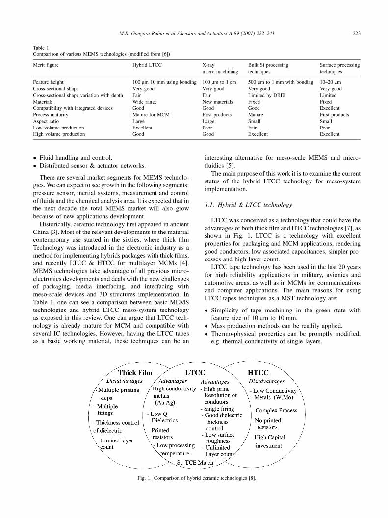
Table 1, one can see a comparison between basic MEMS
technologies and hybrid LTCC meso-system technology
as exposed in this review. One can argue that LTCC tech-
nology is already mature for MCM and compatible with
several IC technologies. However, having the LTCC tapes
as a basic working material, these techniques can be an
interesting alternative for meso-scale MEMS and micro-
¯uidics [5].
The main purpose of this work it is to examine the current
status of the hybrid LTCC technology for meso-system
implementation.
1.1. Hybrid & LTCC technology
LTCC was conceived as a technology that could have the
advantages of both thick ®lm and HTCC technologies [7], as
shown in Fig. 1. LTCC is a technology with excellent
properties for packaging and MCM applications, rendering
good conductors, low associated capacitances, simpler pro-
cesses and high layer count.
LTCC tape technology has been used in the last 20 years
for high reliability applications in military, avionics and
automotive areas, as well as in MCMs for communications
and computer applications. The main reasons for using
LTCC tapes techniques as a MST technology are:
� Simplicity of tape machining in the green state with
feature size of 10 mm to 10 mm.
� Mass production methods can be readily applied.
� Thermo-physical properties can be promptly modified,
e.g. thermal conductivity of single layers.
Table 1
Comparison of various MEMS technologies (modified from [6])
Merit figure Hybrid LTCC X-ray
micro-machining
Bulk Si processing
techniques
Surface processing
techniques
Feature height 100 mm 10 mm using bonding 100 mm to 1 cm 500 mm to 1 mm with bonding 10±20 mm
Cross-sectional shape Very good Very good Very good Very good
Cross-sectional shape variation with depth Fair Fair Limited by DREI Limited
Materials Wide range New materials Fixed Fixed
Compatibility with integrated devices Good Good Good Excellent
Process maturity Mature for MCM First products Mature First products
Aspect ratio Large Large Small Small
Low volume production Excellent Poor Fair Poor
High volume production Good Good Excellent Excellent
Fig. 1. Comparison of hybrid ceramic technologies [8].
M.R. Gongora-Rubio et al. / Sensors and Actuators A 89 (2001) 222±241 223
� Electronic circuits can be integrated because of its hybrid
nature.
� Tapes of different compositions can be formulated to
obtain desired layer properties, e.g. magnetic permeabil-
ity.
� Layer count can be high.
� Possibility of auto-packed devices fabrication.
� Fabrication techniques are relatively simple, inexpensive
and environmentally benign.
Tapes are easily fabricated while still in the green state;
they are soft, pliable, and easily dissolved and abraded.
Once the material is ®red and fully sintered, it becomes
tough and highly rigid. Small structures can be carved and
machined once ®red using diamond tools, and excimer
laser can be utilized to ablade alumina within the smallest
tolerances.
2. LTCC technology
We all know how versatile material silicon can be for the
marriage between microelectronics and MEMS. It has the
right electrical and mechanical properties, of course there is
a price to pay, silicon processing is time consuming, delicate
and very expensive. For larger structures, in the intermediate
size (meso-structures with minimum feature size in the
range from 10 to several hundred microns), it would be
desirable to have a material compatible with hybrid micro-
electronics, with the right thermal, mechanical and electrical
properties, easy to fabricate and inexpensive to process.
LTCC tapes or Green Tapes1 is such a material system.
LTCC tapes are glass-ceramic composite materials. The
ceramic ®ller is usually alumina, Al2O3, but it could be any
other ceramic system, including high thermal conductive
BeO, Ferroelectric Perovskites, ferromagnetic spinels and
`̀ smart'' (photovoltaic-piezoelectric) ceramics. The usual
composition also includes a glass frit binder to lower
processing temperature as well as rendering the material
compatible with thick ®lm technology. A third component of
the composite is an organic vehicle for binding and viscosity
control of the tape before sintering. They are commercially
produced in ¯at tapes of various thicknesses but usually in
the range of 100±400 mm. They are often called green
ceramic tapes because they are manipulated in the green
stage, which is before ®ring and sintering.
To obtain a controlled tape thickness, a doctor blade
machine is used. Such equipment is shown in Fig. 2. Casting
is accomplished by spreading the desired slurry formulation
to form a paste on a moving carrier substrate (usually a ®lm
of cellulose acetate, Te¯on, Mylar, or cellophane) and
removing some of the volatiles. By a soft bake procedure
one obtain a thin, ¯exible tape that can be cut and stamped to
the desire con®guration prior to ®ring.
Although the doctor blade procedure sounds simple, it
requires careful control to avoid warpage, out of tolerance
thickness and other defects. A variety of other additives are
included in the formulation for both aqueous and non-
aqueous doctor blade systems.
One of the important features of green tape technology is
the possibility of fabricating 3D structures using multiple
layers of green tapes [9]. Each layer is fabricated in the green
(before ®ring) with whatever features are needed for the
overall function of the 3D structure. Each layer may have
vias, cavities, channels, and internal electrical elements such
as capacitors, resistors and interconnections. The individual
layers are then arranged in the proper order (stacked), and
placed in a registry to yield the desired structure (see Fig. 3).
The location holes for registry and the vias are usually
punched, although they can be chemically dissolved, etched,
abraded or cut.
The next step consists on moving the stacked blanks to the
press where heat and pressure are applied to complete the
lamination process. At this point the structure is ready for
sintering in air furnace. The complete processing sequence
for LTCC tapes is depicted in Fig. 4.1 Green Tape is a trade mark of DuPont Corporation.
Fig. 2. Schematic depiction of a doctor blade set-up for casting LTCC tapes.
224 M.R. Gongora-Rubio et al. / Sensors and Actuators A 89 (2001) 222±241
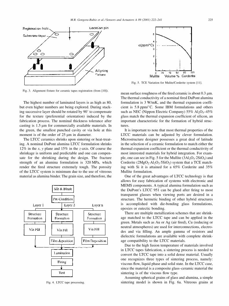
The highest number of laminated layers is as high as 80,
but even higher numbers are being explored. During stack-
ing successive layer should be rotated by 908 to compensate
for the texture (preferential orientation) induced by the
fabrication process. The nominal thickness tolerance after
casting is 1.5 mm for commercially available materials. In
the green, the smallest punched cavity or via hole at this
moment is of the order of 25 mm in diameter.
The LTCC ceramics shrinks upon sintering or heat-treat-
ing. A nominal DuPont alumina LTCC formulation shrinks
12% in the x, y plane and 15% in the z-axis. Of course the
shrinkage is uniform and predictable and one can compen-
sate for the shrinking during the design. The fracture
strength of an alumina formulation is 320 MPa, which
render the ®red structure extremely tough. The porosity
of the LTCC system is minimum due to the use of vitreous
material as alumina binder. The grain size, and therefore, the
mean surface roughness of the ®red ceramic is about 0.3 mm.
The thermal conductivity of a nominal ®red DuPont alumina
formulation is 3 W/mK, and the thermal expansion coef®-
cient is 5.8 ppm/8C. Some IBM formulations and others
such as NEC (Nippon Electric Company) 55% Al2O3±45%
glass match the thermal expansion coef®cient of silicon, an
important characteristic for the formation of hybrid struc-
tures.
It is important to note that most thermal properties of the
LTCC materials can be adjusted by clever formulation.
Microstructure designer possesses a great deal of latitude
in the selection of a ceramic formulation to match either the
thermal expansion coef®cient or the thermal conductivity of
most interested materials for hybrid integration. For exam-
ple, one can see in Fig. 5 for the Mullite (3Al2O3�2SiO2) and
Corderite (2MgO2�Al2O3�5SiO2) system that a TCE match-
ing with Si it is attained for a 65% Corderite and 35%
Mullite formulation.
One of the great advantages of LTCC technology is that
allows for easy fabrication of systems with electronic and
MEMS components. A typical alumina formulation such as
the DuPont's LTCC 951 can be glued after ®ring to most
transparent glasses when viewing ports are desired in a
structure. The hermetic binding of other hybrid structures
is accomplished with die-bonding glass formulations,
epoxies or eutectic bonding.
There are multiple metallization schemes that are shrink-
age matched to the LTCC tape and can be applied in the
green. Metals such as Au or Ag (air ®red), Cu (reducing or
neutral atmospheres) are used for interconnections, electro-
des and via ®lling. An ample gamma of resistors and
dielectric formulations are available with complete shrink-
age compatibility to the LTCC materials.
Due to the high fusion temperature of materials involved
in LTCC tapes fabrication, a sintering process is needed to
convert the LTCC tape into a solid dense material. Usually
one recognizes three types of sintering process, namely:
viscous ¯ow, liquid phase and solid state. In the LTCC case,
since the material is a composite glass±ceramic material the
sintering is of the viscous ¯ow type.
Assuming spherical grains of glass and alumina, a simple
sintering model is shown in Fig. 6a. Vitreous grains at
Fig. 3. Alignment fixture for ceramic tapes registration (from [10]).
Fig. 4. LTCC tape processing.
Fig. 5. TCE Variation for Mulite/Corderite system [11].
M.R. Gongora-Rubio et al. / Sensors and Actuators A 89 (2001) 222±241 225
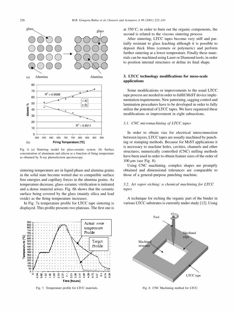
sintering temperature are in liquid phase and alumina grains
in the solid state become wetted due to compatible surface
free energies and capillary forces in the alumina grains. As
temperature decrease, glass±ceramic vitri®cation is initiated
and a dense material arises. Fig. 6b shows that the ceramic
surface being covered by the glass (mainly silica and lead
oxide) as the ®ring temperature increases.
In Fig. 7a temperature pro®le for LTCC tape sintering is
displayed. This pro®le presents two plateaus. The ®rst one is
at 3508C; in order to burn out the organic components, the
second is related to the viscous sintering process.
After sintering, LTCC tapes become very stiff and par-
tially resistant to glass leaching although it is possible to
deposit thick ®lms (cermets or polymeric) and perform
further sintering at a lower temperature. Finally these mate-
rials can be machined using Laser or Diamond tools, in order
to position internal structures or de®ne its ®nal shape.
3. LTCC technology modifications for meso-scaleapplications
Some modi®cations or improvements to the usual LTCC
tape process are needed in order to ful®ll MsST device imple-
mentation requirements. New patterning, sagging control and
lamination procedures have to be developed in order to fully
utilize the potential of LTCC tapes. We have organized these
modi®cations or improvement in eight subsections.
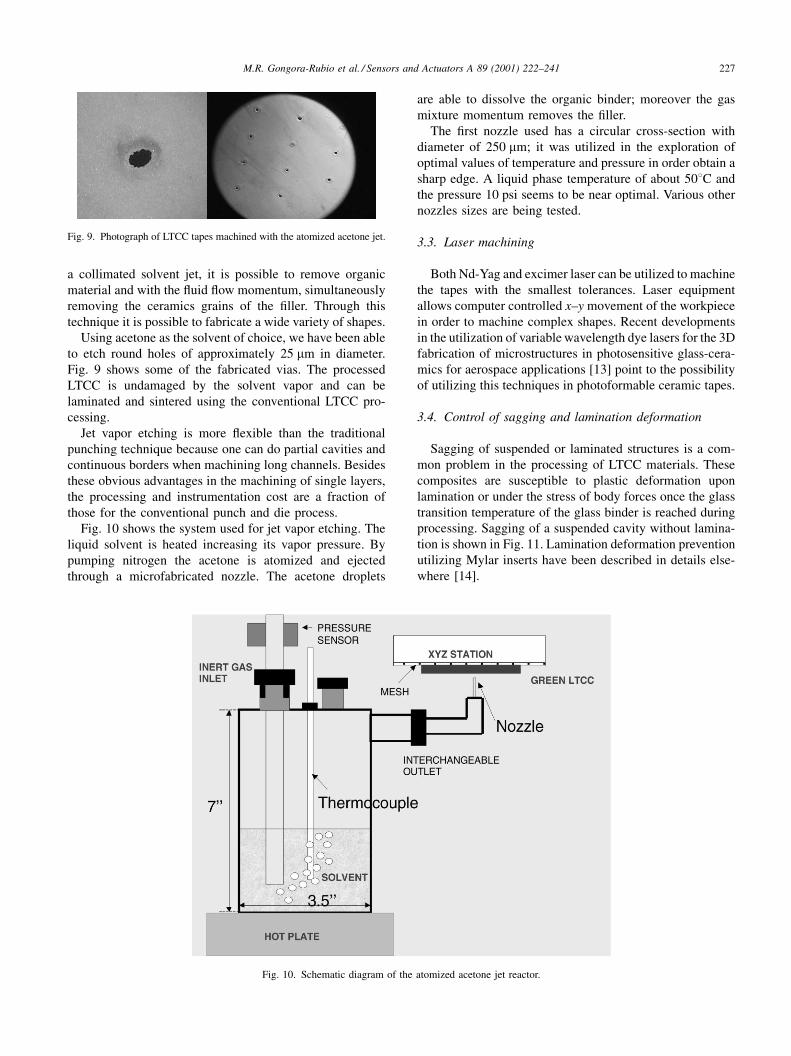
3.1. CNC micromachining of LTCC tapes
In order to obtain vias for electrical interconnection
between layers, LTCC tapes are usually machined by punch-
ing or stamping methods. Because for MsST applications it
is necessary to machine holes, cavities, channels and other
structures; numerically controlled (CNC) milling methods
have been used in order to obtain feature sizes of the order of
100 mm (see Fig. 8).
Using CNC machining, complex shapes are promptly
obtained and dimensional tolerances are comparable to
those of a general-purpose punching machine.
3.2. Jet vapor etching: a chemical machining for LTCC
tapes
A technique for etching the organic part of the binder in
various LTCC substrates is currently under study [12]. Using
Fig. 6. (a) Sintering model for glass-ceramic system. (b) Surface
concentration of aluminum and silicon as a function of firing temperature
as obtained by X-ray photoelectron spectroscopy.
Fig. 7. Temperature profile for LTCC materials. Fig. 8. CNC Machining method for LTCC.
226 M.R. Gongora-Rubio et al. / Sensors and Actuators A 89 (2001) 222±241
a collimated solvent jet, it is possible to remove organic
material and with the ¯uid ¯ow momentum, simultaneously
removing the ceramics grains of the ®ller. Through this
technique it is possible to fabricate a wide variety of shapes.
Using acetone as the solvent of choice, we have been able
to etch round holes of approximately 25 mm in diameter.
Fig. 9 shows some of the fabricated vias. The processed
LTCC is undamaged by the solvent vapor and can be
laminated and sintered using the conventional LTCC pro-
cessing.
Jet vapor etching is more ¯exible than the traditional
punching technique because one can do partial cavities and
continuous borders when machining long channels. Besides
these obvious advantages in the machining of single layers,
the processing and instrumentation cost are a fraction of
those for the conventional punch and die process.
Fig. 10 shows the system used for jet vapor etching. The
liquid solvent is heated increasing its vapor pressure. By
pumping nitrogen the acetone is atomized and ejected
through a microfabricated nozzle. The acetone droplets
are able to dissolve the organic binder; moreover the gas
mixture momentum removes the ®ller.
The ®rst nozzle used has a circular cross-section with
diameter of 250 mm; it was utilized in the exploration of
optimal values of temperature and pressure in order obtain a
sharp edge. A liquid phase temperature of about 508C and
the pressure 10 psi seems to be near optimal. Various other
nozzles sizes are being tested.
3.3. Laser machining
Both Nd-Yag and excimer laser can be utilized to machine
the tapes with the smallest tolerances. Laser equipment
allows computer controlled x±y movement of the workpiece
in order to machine complex shapes. Recent developments
in the utilization of variable wavelength dye lasers for the 3D
fabrication of microstructures in photosensitive glass-cera-
mics for aerospace applications [13] point to the possibility
of utilizing this techniques in photoformable ceramic tapes.
3.4. Control of sagging and lamination deformation
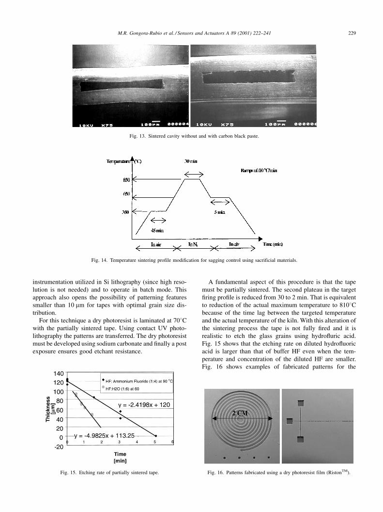
Sagging of suspended or laminated structures is a com-
mon problem in the processing of LTCC materials. These
composites are susceptible to plastic deformation upon
lamination or under the stress of body forces once the glass
transition temperature of the glass binder is reached during
processing. Sagging of a suspended cavity without lamina-
tion is shown in Fig. 11. Lamination deformation prevention
utilizing Mylar inserts have been described in details else-
where [14].
Fig. 9. Photograph of LTCC tapes machined with the atomized acetone jet.
Fig. 10. Schematic diagram of the atomized acetone jet reactor.
M.R. Gongora-Rubio et al. / Sensors and Actuators A 89 (2001) 222±241 227
Among the results obtained is the fact that when an
LTCC tape with holes of diameters in excess of 400 mm
is laminated, the tapes above and below deform in the
inside of the cavity, but for smaller diameters the defor-
mation is negligible. It is reasonable to conclude that the
main cause of sagging is a consequence of the lamination
process.
There are three main strategies used to compensate or
reduce the sagging problem.
3.4.1. Deposition of thick films to compensate
auto-supported structures
In the case of bridging structures, one can compensate for
the potential effect of body forces by screen-printing a thick
®lm, which forms an over-layer with tensile internal stresses
upon sintering [16]. This compensates for the body-force
deformation and often yields straight bridges, as shown in
Fig. 12.
The reason for the effectiveness of this material for
sagging prevention is that the resistor paste is shrinkage
match to ®red alumina substrates which have a higher
coef®cient of thermal expansion than the glass-ceramic tape
used in this study. After sintering, the resistor layer will exert
a tensile force on the interface structure, preventing the
sagging. Note that placement of the thick ®lm is critical as it
is important to match this tensile force to the force inducing
sagging.
3.4.2. Use of sacrificial materials
In this case, the use of a lead bi-silicate frit as a sacri®cial
material can be useful [16]. After deposition and ®ring, the
lead bi-silicate glass is etched in buffered hydro¯uoric acid
in order to remove the material from under the suspended or
bridging structure. Although sacri®cial materials is a good
idea, and have been tested with good results, this method
displays some problems:
� Etching rate is different inside cavities than in open space.
� Due to limited solubility of the glass frit, it is difficult to
remove all the material.
� Ceramic green tapes are glass±ceramic composites and
when exposed to BHF will etch at a rate comparable to the
lead bi-silicate frit.
3.4.3. Use of fugitive phases
The use of fugitive phase materials intended to disappear
during ®ring is another way of supporting bridging struc-
tures [16]. Several of these strategies have been explored.
The idea behind the use of the carbon black as fugitive
phase is to have sintering accomplished in a neutral or just
slightly oxidizing atmosphere. The gasi®cation of the carbon
(reaction with oxygen to form carbon mono, and dioxide) is
slow and little carbon black is lost before the bridging or
suspended ceramic structure becomes rigid. After that point,
one can open the furnace to air and burn-off the carbon
black. Samples were ®red with structures where the feature
size is large enough for the sagging to be evident and easily
measured. After the carbon black gasi®cation and sintering,
the upper and lower layer in the cavity ®lled with the carbon
black-binder mixture are parallel, see Fig. 13.
The compensation can be accomplished by changing the
temperature sintering pro®le and the furnace atmosphere
controlling the air/nitrogen ratio. Fig. 14 shows the sintering
pro®le modi®cation for sagging control, displaying the
regions for air or nitrogen predominance and plateau for
carbon black ®ring.
3.5. Photolithographic patterning of LTCC
These techniques are an emulation of silicon lithography.
The idea is to utilize an inexpensive version of the
Fig. 11. Sagging for suspended cavity without lamination [15].
Fig. 12. Sagging control depositing film on structure.
228 M.R. Gongora-Rubio et al. / Sensors and Actuators A 89 (2001) 222±241
instrumentation utilized in Si lithography (since high reso-
lution is not needed) and to operate in batch mode. This
approach also opens the possibility of patterning features
smaller than 10 mm for tapes with optimal grain size dis-
tribution.
For this technique a dry photoresist is laminated at 708Cwith the partially sintered tape. Using contact UV photo-
lithography the patterns are transferred. The dry photoresist
must be developed using sodium carbonate and ®nally a post
exposure ensures good etchant resistance.
A fundamental aspect of this procedure is that the tape
must be partially sintered. The second plateau in the target
®ring pro®le is reduced from 30 to 2 min. That is equivalent
to reduction of the actual maximum temperature to 8108Cbecause of the time lag between the targeted temperature
and the actual temperature of the kiln. With this alteration of
the sintering process the tape is not fully ®red and it is
realistic to etch the glass grains using hydro¯uric acid.
Fig. 15 shows that the etching rate on diluted hydro¯uoric
acid is larger than that of buffer HF even when the tem-
perature and concentration of the diluted HF are smaller.
Fig. 16 shows examples of fabricated patterns for the
Fig. 13. Sintered cavity without and with carbon black paste.
Fig. 14. Temperature sintering profile modification for sagging control using sacrificial materials.
Fig. 15. Etching rate of partially sintered tape. Fig. 16. Patterns fabricated using a dry photoresist film (RistonTM).
M.R. Gongora-Rubio et al. / Sensors and Actuators A 89 (2001) 222±241 229
development of a multilayer coil and an eletrophoretic
channel utilizing this technique.
Multilayer structures can be accomplished modifying the
standard lamination process as follows:
� Stack, alignment (using registration marks previously
patterned).
� Sintering of the assembly using a low-pressure jig.
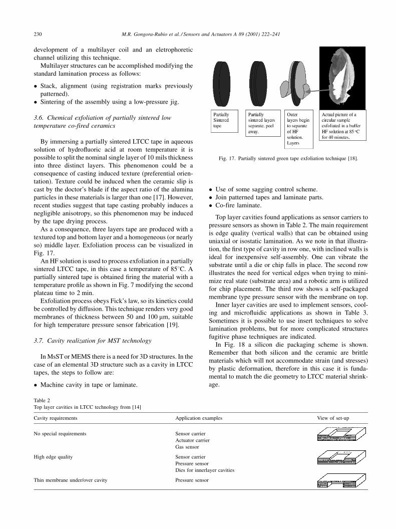
3.6. Chemical exfoliation of partially sintered low
temperature co-fired ceramics
By immersing a partially sintered LTCC tape in aqueous
solution of hydro¯uoric acid at room temperature it is
possible to split the nominal single layer of 10 mils thickness
into three distinct layers. This phenomenon could be a
consequence of casting induced texture (preferential orien-
tation). Texture could be induced when the ceramic slip is
cast by the doctor's blade if the aspect ratio of the alumina
particles in these materials is larger than one [17]. However,
recent studies suggest that tape casting probably induces a
negligible anisotropy, so this phenomenon may be induced
by the tape drying process.
As a consequence, three layers tape are produced with a
textured top and bottom layer and a homogeneous (or nearly
so) middle layer. Exfoliation process can be visualized in
Fig. 17.
An HF solution is used to process exfoliation in a partially
sintered LTCC tape, in this case a temperature of 858C. A
partially sintered tape is obtained ®ring the material with a
temperature pro®le as shown in Fig. 7 modifying the second
plateau time to 2 min.
Exfoliation process obeys Fick's law, so its kinetics could
be controlled by diffusion. This technique renders very good
membranes of thickness between 50 and 100 mm, suitable
for high temperature pressure sensor fabrication [19].
3.7. Cavity realization for MST technology
In MsST or MEMS there is a need for 3D structures. In the
case of an elemental 3D structure such as a cavity in LTCC
tapes, the steps to follow are:
� Machine cavity in tape or laminate.
� Use of some sagging control scheme.
� Join patterned tapes and laminate parts.
� Co-fire laminate.
Top layer cavities found applications as sensor carriers to
pressure sensors as shown in Table 2. The main requirement
is edge quality (vertical walls) that can be obtained using
uniaxial or isostatic lamination. As we note in that illustra-
tion, the ®rst type of cavity in row one, with inclined walls is
ideal for inexpensive self-assembly. One can vibrate the
substrate until a die or chip falls in place. The second row
illustrates the need for vertical edges when trying to mini-
mize real state (substrate area) and a robotic arm is utilized
for chip placement. The third row shows a self-packaged
membrane type pressure sensor with the membrane on top.
Inner layer cavities are used to implement sensors, cool-
ing and micro¯uidic applications as shown in Table 3.
Sometimes it is possible to use insert techniques to solve
lamination problems, but for more complicated structures
fugitive phase techniques are indicated.
In Fig. 18 a silicon die packaging scheme is shown.
Remember that both silicon and the ceramic are brittle
materials which will not accommodate strain (and stresses)
by plastic deformation, therefore in this case it is funda-
mental to match the die geometry to LTCC material shrink-
age.
Fig. 17. Partially sintered green tape exfoliation technique [18].
Table 2
Top layer cavities in LTCC technology from [14]
Cavity requirements Application examples View of set-up
No special requirements Sensor carrier
Actuator carrier
Gas sensor
High edge quality Sensor carrier
Pressure sensor
Dies for innerlayer cavities
Thin membrane under/over cavity Pressure sensor
230 M.R. Gongora-Rubio et al. / Sensors and Actuators A 89 (2001) 222±241
3.8. Bonding of LTCC tapes with other materials
It is possible to bond LTCC Tapes to other materials, like,
glass, ceramics, metals and silicon, using a co-®red or post-
®red scheme. This technology is fully compatible with thick
®lm and some thin ®lm technologies.
Glass is bonded using a co-®red scheme or through post-
®red glass frits and lower sintering temperatures. Several
epoxides could also be used in some applications. For
ceramics in particular, one can bond using co-®ring frits
and glazes, epoxy or brazing techniques. Silicon can be co-
®red or post-®red using metallic die-attaching pastes.
3.8.1. Constrained lamination and sintering
When a green LTCC tape is laminated to a rigid substrate
(e.g. metal, ceramic or others) the xy shrinkage is negligible.
All the change in volume is accomplished by shrinkage in
the z-direction. Fig. 19 depicts ®ve ®red layers laminated to a
rigid alumina substrate. Note the asymptotic behavior
toward the nominal percentage shrinkage value as we move
further away from the substrate.
4. Photoformable LTCC tapes
We would like to report some results on a photosensitive
dielectric ceramic tape prototype. The photoformable cera-
mic incorporates a photopolymer in the organic binder. This
material is a glass ceramic composite with a conventional
nominal composition except that in the organics, besides the
plasticizers and ani¯oculants, a negative photoresist is in-
cluded. The photosensitive tape we utilized was 150 mm thick.
The processing sequence for photoformable LTCC tape is
depicted in Fig. 20.
Table 3
Inner layer cavities in LTCC technology from [14]
Cavity requirements Application examples View of set-up
Simple through holes (x- or y-direction) Flow sensor
Cooling functions
Small capillary tubes Chemical sensor
Capillary systems Cooling systems
Microfluidic systems
Expanded innerlayer cavities Pressure sensor
Chemical sensor
Fig. 18. Schematic and samples for packaging of silicon dies in LTCC tapes.
Fig. 19. Z-shrinkage behavior in a multilayer structure under constrained lamination and sintering.
M.R. Gongora-Rubio et al. / Sensors and Actuators A 89 (2001) 222±241 231
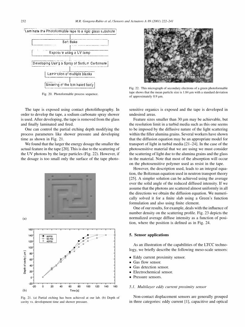
The tape is exposed using contact photolithography. In
order to develop the tape, a sodium carbonate spray shower
is used. After developing, the tape is removed from the glass
and ®nally laminated and ®red.
One can control the partial etching depth modifying the
process parameters like shower pressure and developing
time as shown in Fig. 21.
We found that the larger the energy dosage the smaller the
actual feature in the tape [20]. This is due to the scattering of
the UV photons by the large particles (Fig. 22). However, if
the dosage is too small only the surface of the tape photo-
sensitive organics is exposed and the tape is developed in
undesired areas.
Feature sizes smaller than 30 mm may be achievable, but
the resolution limit in a turbid media such as this one seems
to be imposed by the diffusive nature of the light scattering
within the ®ller alumina grains. Several workers have shown
that the diffusion equation may be an appropriate model for
transport of light in turbid media [21±24]. In the case of the
photosensitive material that we are using we must consider
the scattering of light due to the alumina grains and the glass
in the material. Note that most of the absorption will occur
on the photosensitive polymer used as resist in the tape.
However, the description used, leads to an integral equa-
tion, the Boltzman equation used in neutron transport theory
[25]. A simpler solution can be achieved using the average
over the solid angle of the reduced diffused intensity. If we
assume that the photons are scattered almost uniformly in all
the directions we obtain the diffusion equation. We numeri-
cally solved it for a ®nite slab using a Green's function
formulation and also using ®nite element.
One of our results, for example, deals with the in¯uence of
number density on the scattering pro®le. Fig. 23 depicts the
normalized average diffuse intensity as a function of posi-
tion, where the position is de®ned as in Fig. 24.
5. Sensor applications
As an illustration of the capabilities of the LTCC techno-
logy, we brie¯y describe the following meso-scale sensors:
� Eddy current proximity sensor.
� Gas flow sensor.
� Gas detection sensor.
� Electrochemical sensor.
� Pressure sensors.
5.1. Multilayer eddy current proximity sensor
Non-contact displacement sensors are generally grouped
in three categories: eddy current [1], capacitive and optical
Fig. 20. Photoformable process sequence.
Fig. 21. (a) Partial etching has been achieved at our lab. (b) Depth of
cavity vs. development time and shower pressure.
Fig. 22. This micrograph of secondary electrons of a green photoformable
tape shows that the mean particle size is 1.84 mm with a standard deviation
of approximately 0.9 mm.
232 M.R. Gongora-Rubio et al. / Sensors and Actuators A 89 (2001) 222±241
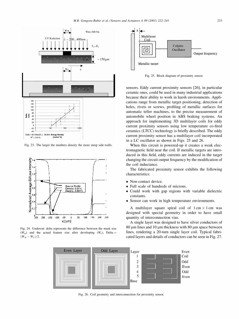
sensors. Eddy current proximity sensors [26], in particular
ceramic ones, could be used in many industrial applications
because their ability to work in harsh environments. Appli-
cations range from metallic target positioning, detection of
holes, rivets or screws, pro®ling of metallic surfaces for
automatic teller machines, to the precise measurement of
automobile wheel position in ABS braking systems. An
approach for implementing 3D multilayer coils for eddy
current proximity sensors using low temperature co-®red
ceramics (LTCC) technology is brie¯y described. The eddy
current proximity sensor has a multilayer coil incorporated
in a LC oscillator as shown in Figs. 25 and 26.
When this circuit is powered-up it creates a weak elec-
tromagnetic ®eld near the coil. If metallic targets are intro-
duced in this ®eld, eddy currents are induced in the target
changing the circuit output frequency by the modi®cation of
the coil inductance.
The fabricated proximity sensor exhibits the following
characteristics:
� Non-contact device.
� Full scale of hundreds of microns.
� Could work with gap regions with variable dielectric
constants.
� Sensor can work in high temperature environments.
A multilayer square spiral coil of 1 cm� 1 cm was
designed with special geometry in order to have small
quantity of interconnection vias.
A single layer was designed to have silver conductors of
80 mm lines and 10 mm thickness with 80 mm space between
lines, rendering a 20-turn single layer coil. Typical fabri-
cated layers and details of conductors can be seen in Fig. 27.
Fig. 23. The larger the numbers density the more steep side-walls.
Fig. 24. Undercut: delta represents the difference between the mask size
(Wm) and the actual feature size after developing (Wc), Delta ��Wm ÿWc�=2.
Fig. 25. Block diagram of proximity sensor.
Fig. 26. Coil geometry and interconnection for proximity sensor.
M.R. Gongora-Rubio et al. / Sensors and Actuators A 89 (2001) 222±241 233
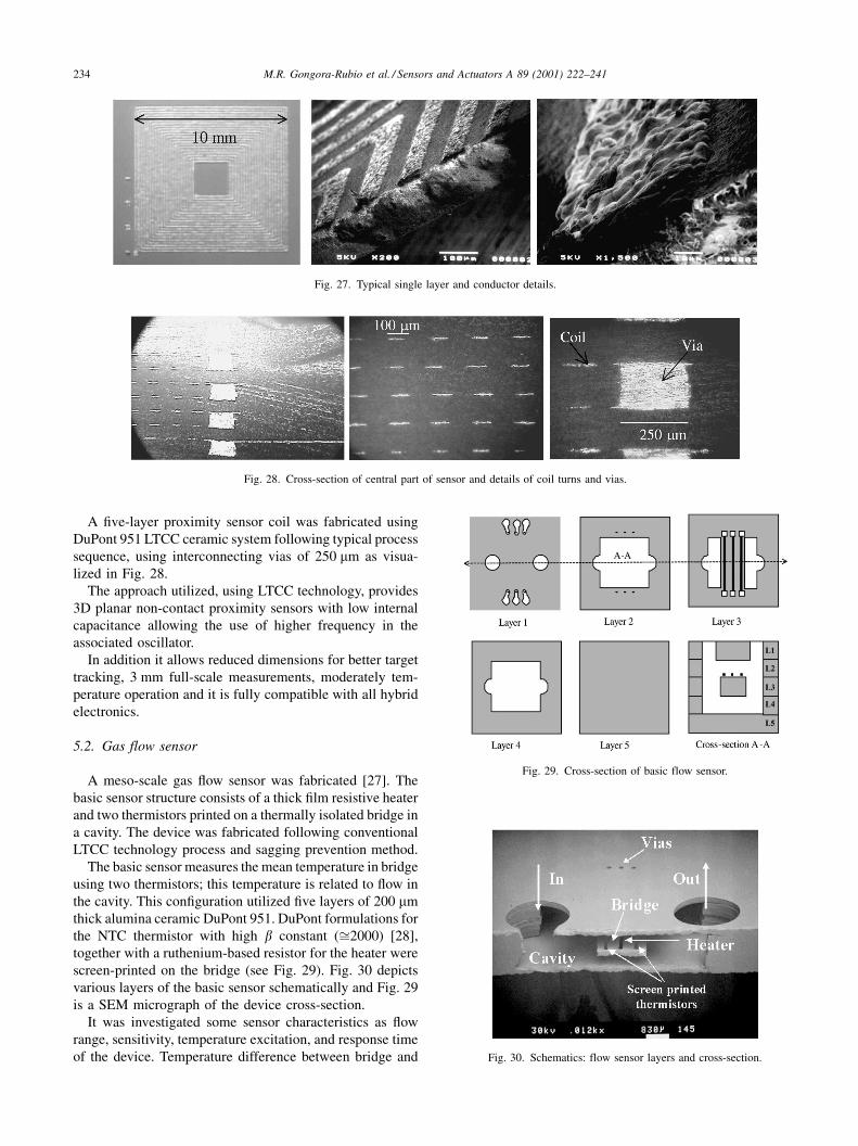
A ®ve-layer proximity sensor coil was fabricated using
DuPont 951 LTCC ceramic system following typical process
sequence, using interconnecting vias of 250 mm as visua-
lized in Fig. 28.
The approach utilized, using LTCC technology, provides
3D planar non-contact proximity sensors with low internal
capacitance allowing the use of higher frequency in the
associated oscillator.
In addition it allows reduced dimensions for better target
tracking, 3 mm full-scale measurements, moderately tem-
perature operation and it is fully compatible with all hybrid
electronics.
5.2. Gas flow sensor
A meso-scale gas ¯ow sensor was fabricated [27]. The
basic sensor structure consists of a thick ®lm resistive heater
and two thermistors printed on a thermally isolated bridge in
a cavity. The device was fabricated following conventional
LTCC technology process and sagging prevention method.
The basic sensor measures the mean temperature in bridge
using two thermistors; this temperature is related to ¯ow in
the cavity. This con®guration utilized ®ve layers of 200 mm
thick alumina ceramic DuPont 951. DuPont formulations for
the NTC thermistor with high b constant (�2000) [28],
together with a ruthenium-based resistor for the heater were
screen-printed on the bridge (see Fig. 29). Fig. 30 depicts
various layers of the basic sensor schematically and Fig. 29
is a SEM micrograph of the device cross-section.
It was investigated some sensor characteristics as ¯ow
range, sensitivity, temperature excitation, and response time
of the device. Temperature difference between bridge and
Fig. 27. Typical single layer and conductor details.
Fig. 28. Cross-section of central part of sensor and details of coil turns and vias.
Fig. 29. Cross-section of basic flow sensor.
Fig. 30. Schematics: flow sensor layers and cross-section.
234 M.R. Gongora-Rubio et al. / Sensors and Actuators A 89 (2001) 222±241

¯uid temperature as a function of the heater current is
displayed in Fig. 31. Fig. 32 indicates dissipation factor
of the fabricated device to diverse ¯ow velocities [29].
5.3. Gas detection sensor
Gas sensor devices using SnO2 has been implemented
using LTCC technology by Teterycz et al. [30]. Sensors were
made using LTCC techniques with a platinum heater buried
inside the multilayer structure. Tin oxide or thick ®lms SnO2
with Pd as catalyst were used as gas sensitive materials. The
properties of the gas sensors were measured with methane
and carbon monoxide.
5.4. Electrochemical sensor
A new electrochemical technique, temperature pulse vol-
tammetry (TPV), was recently introduced using an electrode
array fabricated with LTCC technology [31]. Working,
counter and reference electrodes were screen-printed on
an LTCC tape using Au, Pt, and Ag/AgCl pastes, respec-
tively. The thermal conductivity of the ceramic substrate is
®ve times higher than that of water, which helps to better
control the electrode temperatures.
5.5. Pressure sensors
LTCC tape based pressure sensors of the membrane type
have also been developed. In our case, to obtain the mem-
brane we utilize the LTCC tape exfoliation process described
in Section 3. The sensing device uses piezoresistors from
hybrid pastes. These sensors have the advantage of being
selfpackaged and to withstand high temperatures [32].
LTCC tapes also allows for onboard electronics [33].
6. Some microfluidic devices
Simplicity to implement channels is one of LTCC tech-
nology characteristics. Cavities with reduced dimension and
without geometrical limitations can be achieved [34]. In this
section some basic applications in the micro¯uidics area are
presented, speci®cally microchannel, a critical ori®ce and a
gas ¯ow sensor fabrication.
6.1. Microchannels
First studies on microchannels were performed by Poi-
seuille [35] in 1846. He managed to do some experiments
using glass capillaries with diameters in the hundreds of
microns. From this study the classical expression that relates
pressure drop with volumetric ¯ow rate was obtained.
Microchannels on silicon substrates were studied by Phaler
[36] and Harley et al. [37] to relate hydraulic diameter with
liquid and gas behavior. Fig. 33 illustrate a simple way to
Fig. 31. Delta T vs. flow with parameter Ip.
Fig. 32. Dissipation factor vs. flow.
Fig. 33. L microchannel and implementation of Y microchannel using LTCC technology.
M.R. Gongora-Rubio et al. / Sensors and Actuators A 89 (2001) 222±241 235
implement microchannels using LTCC tape technology; in
this case three layers are enough to fabricate the channel.
Top layer makes media interconnection, middle layer makes
the channel itself (that could be straight, in L, Y, U, spiral or
any desired complex shape), and bottom layer makes the
device base. A Y-shaped microchannel fabricated using
LTCC tapes and glass, it is also presented.
Measurements performed by Moon et al. [38] in straight
conduits with dimensions shown in Fig. 34 display linear
pressure drop for low Reynolds numbers.
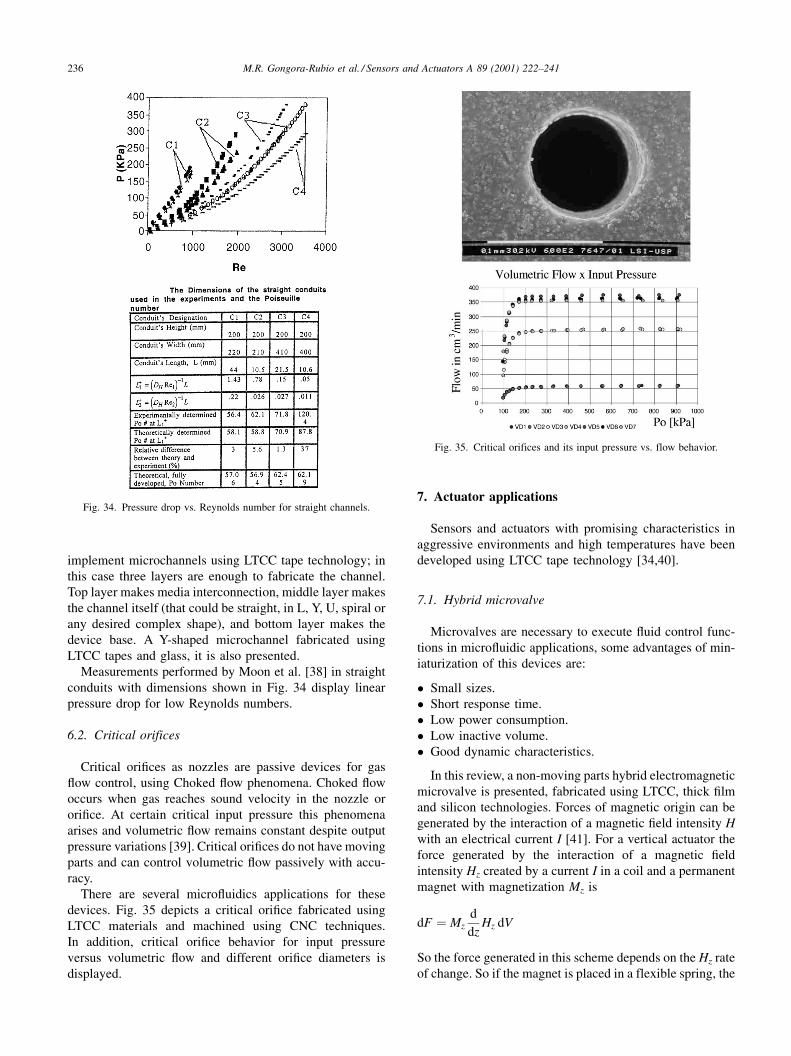
6.2. Critical orifices
Critical ori®ces as nozzles are passive devices for gas
¯ow control, using Choked ¯ow phenomena. Choked ¯ow
occurs when gas reaches sound velocity in the nozzle or
ori®ce. At certain critical input pressure this phenomena
arises and volumetric ¯ow remains constant despite output
pressure variations [39]. Critical ori®ces do not have moving
parts and can control volumetric ¯ow passively with accu-
racy.
There are several micro¯uidics applications for these
devices. Fig. 35 depicts a critical ori®ce fabricated using
LTCC materials and machined using CNC techniques.
In addition, critical ori®ce behavior for input pressure
versus volumetric ¯ow and different ori®ce diameters is
displayed.
7. Actuator applications
Sensors and actuators with promising characteristics in
aggressive environments and high temperatures have been
developed using LTCC tape technology [34,40].
7.1. Hybrid microvalve
Microvalves are necessary to execute ¯uid control func-
tions in micro¯uidic applications, some advantages of min-
iaturization of this devices are:
� Small sizes.
� Short response time.
� Low power consumption.
� Low inactive volume.
� Good dynamic characteristics.
In this review, a non-moving parts hybrid electromagnetic
microvalve is presented, fabricated using LTCC, thick ®lm
and silicon technologies. Forces of magnetic origin can be
generated by the interaction of a magnetic ®eld intensity H
with an electrical current I [41]. For a vertical actuator the
force generated by the interaction of a magnetic ®eld
intensity Hz created by a current I in a coil and a permanent
magnet with magnetization Mz is
dF � Mz
d
dzHz dV
So the force generated in this scheme depends on the Hz rate
of change. So if the magnet is placed in a flexible spring, the
Fig. 34. Pressure drop vs. Reynolds number for straight channels.
Fig. 35. Critical orifices and its input pressure vs. flow behavior.
236 M.R. Gongora-Rubio et al. / Sensors and Actuators A 89 (2001) 222±241
applied force will be [42]
Fz � Mz
Zd
dzHz dV
Hz for given geometry can be calculated integrating the
Biot±Savart law. As a result of this force, the spring generate
a displacement proportional to the force divided by the
equivalent spring constant k.
Dz � Fzkÿ1
Electromagnetic techniques are suitable to hybrid meso-
systems, [43,44] because:
� Can generate large forces.
� Can produce large displacements.
� Good performance with temperature.
� Adequate velocity response.
� Robust and inexpensive technique.
A hybrid microvalve was implemented using LTCC. This
device has a multilayer coil, a ¯uidic system and a ¯exible
diaphragm with a permanent magnet bonded in its topside,
as shown in Fig. 36.
The multilayer coil fabrication is similar to that used in
the proximity sensor presented above. The ¯uidic part of the
system can be implemented with three LTCC tapes as
presented in Fig. 37.
Flexible diaphragm with a rare earth magnet attached
allows for electromagnetic actuation; the diaphragm was
implemented using silicon technology for a planar spiral
spring that is covered with an RTV ®lm. Fig. 38 depicts the
¯exible diaphragm fabrication process. Fig. 39 illustrates the
actual microfabricated ¯exible diaphragms (planar spring);
one can also see the complete devices after bonding the rare
earth magnet.
The fabricated microvalve is shown in Fig. 40. This is
a hybrid device that utilizes LTCC tape, an electro-magnet,
a ¯uid ¯ow manifold, an anisotropically etched silicon
Fig. 36. Conception of a hybrid microvalve.
Fig. 37. Microvalve fluidic system.
Fig. 38. Flexible-diaphragm fabrication process.
M.R. Gongora-Rubio et al. / Sensors and Actuators A 89 (2001) 222±241 237
rectangular planar spring, and a high energy product SmCo
mini-permanent magnet. Device dimensions are in the meso
(intermediate) range with the smallest features (¯uid conduit
in the manifold) of 400 mm and the largest (the electro-
magnet, coil) of 12 mm. All parts of the electromagnet and
the channels were machined from DuPont 951 series utiliz-
ing either a numerically controlled milling machine, a
puncher or an isotropic etching technique involving the
glassy binder of a partially sintered LTCC tape. The coil
consists of ®ve layers of planar spiral. The total coil resis-
tance is high (120 O) and thermal considerations limit the
current to 150 mA.
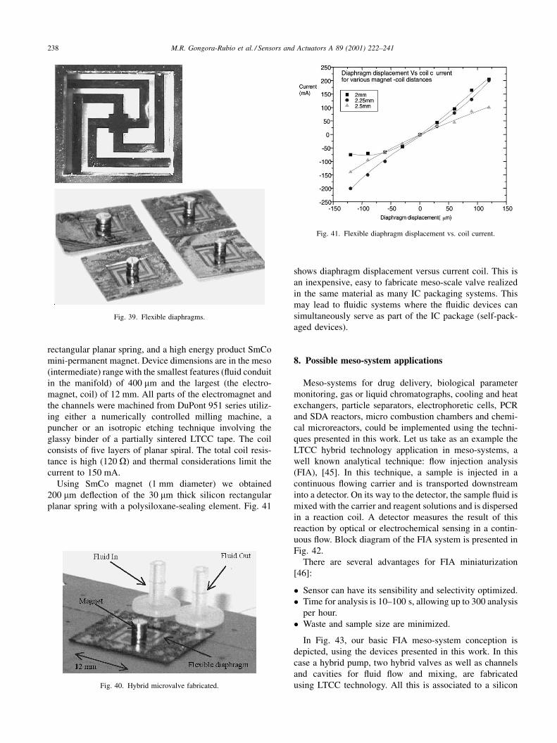
Using SmCo magnet (1 mm diameter) we obtained
200 mm de¯ection of the 30 mm thick silicon rectangular
planar spring with a polysiloxane-sealing element. Fig. 41
shows diaphragm displacement versus current coil. This is
an inexpensive, easy to fabricate meso-scale valve realized
in the same material as many IC packaging systems. This
may lead to ¯uidic systems where the ¯uidic devices can
simultaneously serve as part of the IC package (self-pack-
aged devices).
8. Possible meso-system applications
Meso-systems for drug delivery, biological parameter
monitoring, gas or liquid chromatographs, cooling and heat
exchangers, particle separators, electrophoretic cells, PCR
and SDA reactors, micro combustion chambers and chemi-
cal microreactors, could be implemented using the techni-
ques presented in this work. Let us take as an example the
LTCC hybrid technology application in meso-systems, a
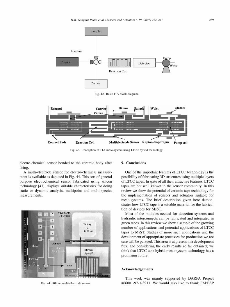
well known analytical technique: ¯ow injection analysis
(FIA), [45]. In this technique, a sample is injected in a
continuous ¯owing carrier and is transported downstream
into a detector. On its way to the detector, the sample ¯uid is
mixed with the carrier and reagent solutions and is dispersed
in a reaction coil. A detector measures the result of this
reaction by optical or electrochemical sensing in a contin-
uous ¯ow. Block diagram of the FIA system is presented in
Fig. 42.
There are several advantages for FIA miniaturization
[46]:
� Sensor can have its sensibility and selectivity optimized.
� Time for analysis is 10±100 s, allowing up to 300 analysis
per hour.
� Waste and sample size are minimized.
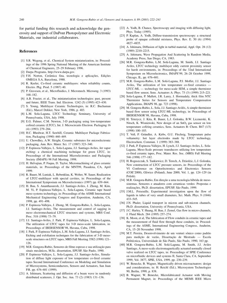
In Fig. 43, our basic FIA meso-system conception is
depicted, using the devices presented in this work. In this
case a hybrid pump, two hybrid valves as well as channels
and cavities for ¯uid ¯ow and mixing, are fabricated
using LTCC technology. All this is associated to a silicon
Fig. 39. Flexible diaphragms.
Fig. 40. Hybrid microvalve fabricated.
Fig. 41. Flexible diaphragm displacement vs. coil current.
238 M.R. Gongora-Rubio et al. / Sensors and Actuators A 89 (2001) 222±241
electro-chemical sensor bonded to the ceramic body after
®ring.
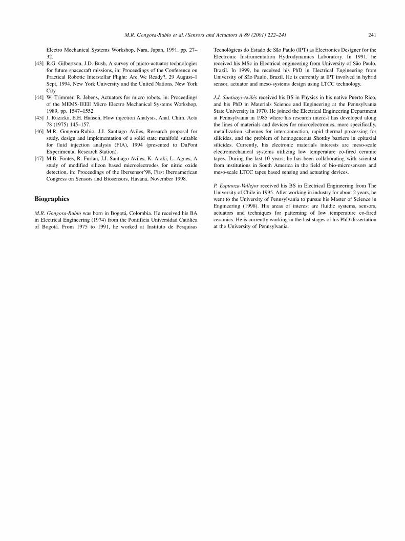
A multi-electrode sensor for electro-chemical measure-
ment is available as depicted in Fig. 44. This sort of general
purpose electrochemical sensor fabricated using silicon
technology [47], displays suitable characteristics for doing
static or dynamic analysis, multipoint and multi-species
measurements.
9. Conclusions
One of the important features of LTCC technology is the
possibility of fabricating 3D structures using multiple layers
of LTCC tapes. In spite of all their attractive features, LTCC
tapes are not well known in the sensor community. In this
review we show the potential of ceramic tape technology for
the implementation of sensors and actuators suitable for
meso-systems. The brief description given here demon-
strates how LTCC tape is a suitable material for the fabrica-
tion of devices for MsST.
Most of the modules needed for detection systems and
hydraulic interconnects can be fabricated and integrated in
green tapes. In this review we show a sample of the growing
number of applications and potential applications of LTCC
tapes to MsST. Studies of more such applications and the
development of appropriate processes for production we are
sure will be pursued. This area is at present in a development
¯ux, and considering the early results so far obtained; we
think that LTCC tape hybrid meso-system technology has a
promising future.
Acknowledgements
This work was mainly supported by DARPA Project
#66001-97-1-8911. We would also like to thank FAPESP
Fig. 42. Basic FIA block diagram.
Fig. 43. Conception of FIA meso-system using LTCC hybrid technology.
Fig. 44. Silicon multi-electrode sensor.
M.R. Gongora-Rubio et al. / Sensors and Actuators A 89 (2001) 222±241 239
for partial funding this research and acknowledge the gen-
erosity and support of DuPont Photopolymer and Electronic
Materials, our industrial collaborators.
References
[1] S.R. Wegeng, et al., Chemical System miniaturization, in: Proceed-
ings of the 1996 Spring National Meeting of the American Institute
of Chemical Engineers, 25±29 February 1996.
[2] Darpa Programs, http://www.darpa.gov.
[3] F.H. Norton, CeraÃmica fina, tecnologia e aplicacËoÄes, EdicËoÄes
OMEGA S.A, Barcelona, 1988.
[4] R. Keeler, Co-fired ceramic multilayers: when reliability counts,
Electro. Pkg. Prod. 5 (1987) 40.
[5] P. Gravesen, et al., Microfluidics, J. Micromech. Microeng. 3 (1993)
168±182.
[6] A.B. Frazier, et al., The miniaturization technologies: past, present
and future, IEEE Trans. Ind. Electron. 1242 (5) (1995) 423±430.
[7] S. Young, Multilayer Ceramic Technologies, in: R.C. Buchaman
(Ed.), Marcel Dekker, New York, 1986, p. 403.
[8] L.M. Sola-Laguna, LTCC Technology Seminary, University of
Pennsylvania, USA, July 1998.
[9] E.G. Palmer, C.M. Newton, 3-D packaging using low-temperature
cofired ceramic (LTCC), Int. J. Microcircuits Electron. Packaging 16
(4) (1993) 279±284.
[10] H.C. Bhedwar, H.T. Sawhill, Ceramic Multilayer Package Fabrica-
tion, Packaging (1990) 460±469.
[11] U. Chowdhry, A.W. Sleight, Ceramic substrates for microelectronic
packaging, Ann. Rev. Mater. Sci. 17 (1987) 323±340.
[12] P. Espinoza-Vallejos, L. Sola-Laguna, J.J. Santiago-Aviles, Jet vapor
etching: a chemical machining technique for green LTCC, in:
Proceedings of the International Microelectronics and Packaging
Society (IMAPS) 98 Fall Meeting, 1998.
[13] H. Helvajian, P. Fuqua, D. Taylor, Micromachining of glass ceramic
materials, in: Proceedings of the MNT99, Pasadena, CA, April
1999.
[14] R. Bauer, M. Luniak, L. Rebenklau, K. Wolter, W. Sauer, Realization
of LTCC-multilayer with special cavities, in: Proceedings of the
International Symposium on Microelectronics (1997) pp. 659±664.
[15] H. Bau, S. Ananthasuresh, J.J. Santiago-Aviles, J. Zhong, M. Kim,
M. Yi, P. Espinoza-Vallejos, L. Sola-Laguna, Ceramic tape based
meso systems technology, in: Proceedings of the ASME International
Mechanical Engineering Congress and Exposition, Anaheim, CA,
1998, pp. 491±498.
[16] P. Espinoza-Vallejos, J. Zhong, M. Gongora-Rubio, L. Sola-Laguna,
J.J. Santiago-Aviles, The measurement and control of sagging in
meso electromechanical LTCC structures and systems, MRS Conf.
Proc. 518 (1998) 73±79.
[17] J.J. Santiago-Aviles, J. Park, P. Espinoza-Vallejos, L. Sola-Laguna,
The utilization of LTCC tapes for 3-D meso-scale fabrication, in:
Proceedings of IBERSENSOR'98, Havana, Cuba, 1998.
[18] J. Park, P. Espinoza-Vallejos, L.M. Sola-Laguna, J.J. Santiago-Aviles,
Etching and exfoliation techniques for the fabrication of 3-D meso-
scale structures on LTCC tapes, MRS Fall Meeting 3582 (1998) 121±
126.
[19] M.R. Gongora-Rubio, Sensores de filme espesso e sua utilizacËaÄo para
sinais mecaÃnicos, M.Sc. dissertation, EPUSP, SaÄo Paulo, 1990.
[20] P. Espinoza-Vallejos, L. Sola-Laguna, J.J. Santiago-Aviles, Simula-
tion of diffuse light exposure of low temperature co-fired ceramic
tapes Second International Conference on Modeling and Simulation
of Microsystems, Semiconductors, Sensors and Actuators, San Juan
P.R. pp. 676±681 (1999).
[21] A. Ishimaru, Scattering and diffusion of a beam wave in randomly
distributed scatterers, J. Opt. Soc. Am. 73 (2) (1983) 131±136.
[22] A. Yodh, B. Chance, Spectroscopy and imaging with diffusing light,
Phys. Today (1995).
[23] P. Kaplan, A. Yodh, Diffuse-transmission spectroscopy: a structural
probe of opaque colloidal mixtures, Phys. Rev. E. 50 (6) (1994)
4827±4835.
[24] A. Ishimaru, Diffusion of light in turbid material, Appl. Opt. 28 (12)
(1989) 2210±2215.
[25] A. Ishimaru, Wave Propagation And Scattering In Random Media,
Academy Press, San Diego, CA, 1983.
[26] M.R. Gongora-Rubio, L.M. SolaÂ-Laguna, M. Smith, J.J. Santiago
Aviles, LTCC technology multilayer eddy current proximity sensor
for harsh environments, in: Proceedings of the 32nd International
Symposium on Microelectronics, IMAPS'99, 26±28 October 1999,
Chicago, IL, pp. 676±681.
[27] M.R. Gongora-Rubio, L.M. SolaÂ-Laguna, P.J. Moffet, J.J. Santiago
Aviles, The utilization of low temperature co-fired ceramics Ð
LTCC-ML Ð technology for meso-scale SEM, a simple thermistor
based flow sensor, Sens. Actuators A: Phys. 73 (3) (1999) 215±221.
[28] Sola-Laguna, P. Mallett, J.R. Larey, J. Hormadaly, thick film NTC
Thermistor Series for Sensors and Temperature Compensation
Applications, IMAPS 98, pp. 723 (1998).
[29] M. Gongora-Rubio, L. Sola, J.J. Santiago-AvileÂs, A simple thermistor
based flow sensor using LTCC-ML technology, in: Proceedings of
IBERSENSOR'98, Havana, Cuba, 1998.
[30] H. Teterycz, J. Kita, R. Bauer, L.J. Golonka, B.W. Licznerski, K.
Nitsch, K. Wisniewski, New design of an SnO2 gas sensor on low
temperature cofiring ceramics, Sens. Actuators B: Chem. B47 (1/3)
(1998) 100±103.
[31] T. Veû, P. GruÈndler, A. Kirbs, G.U. Flechsig, Temperature pulse
voltametry: hot layer electrodes made by LTCC technology,
Electrochem. Commun. 1 (1999) 383±388.
[32] J. Park, P. Espinoza-Vallejos, H. Lynch, J.J. Santiago-Aviles, L. Sola-
Laguna, Meso-Scale pressure transducers utilizing low temperature
co-fired ceramic tapes, Proc. Mater. Res. Soc. (MRS) Fall Meeting
546 (1998) 177±182.
[33] H. Roguszczak, S. Tankiewicz, D. Terech, A. Dziedzic, L.J. Golonka,
New construction of LTCC pressure sensors, in: Proceedings of the
VI Conference on Optoelectronics and Electronics Sensors
(COE'2000), Gliwice (Poland), June 2000, Vol. 1, pp. 124±129 (in
Polish).
[34] M.R. Gongora-Rubio, Em direcËaÄo a uma tecnologia hõÂbrida de meso-
sistemas. Sensores e atuadores com ceramicas verdes: Propostas e
realizacËoÄes, Ph.D. dissertation, EPUSP, SaÄo Paulo, 1999.
[35] J.M.L. Poiseuille, Experimental investigation upon the flow of
liquids in tubes of very small diameters, Sci. Math. Phys. 9 (1846)
433±545.
[36] J.N. Phaler, Liquid transport in micron and sub-micron channels,
Ph.D. dissertation, University of Pennsylvania, USA.
[37] J.C. Harley, Y. Huang, H. Bau, J. Zemel, Gas flow in micro-channels,
J. Fluid Mech. 284 (1995) 257±274.
[38] K. Moon, et al, The fabrication of Flow conduits in ceramic tapes and
the measurement of fluid flow through these conduits, in: Proceed-
ings of the ASME, International Engineering Congress, Anaheim,
CA, 15±20 November 1998.
[39] M.T. Pereira, Desenvolvimento de um venturi soÃnico como padraÄo
para medicËaÄo de vazaÄo, DissertacËaÄo de Mestrado Ð Escola
PoliteÂcnica, Universidade de SaÄo Paulo, SaÄo Paulo, 1990, 163 pp.
[40] M.R. Gongora-Rubio, L.M. SolaÂ-Laguna, M. Smith, J.J. Aviles
Santiago, A meso-scale electromagnetically actuated normally closed
valve realized on LTCC tapes, in: Proceedings of SPIE Conference
on microfluidic devices and systems II, Santa Clara, CA, September
1999, Vol. 3877, SPIE, USA, 1999, pp. 230±239.
[41] W. Benecke, B. Wagner, Magnetically driven microactuators: design
and considerations, in: H. Reichl (Ed.), Microsystem Technologies
90, Berlin, 1990, p. 838.
[42] B. Wagner, W. Benecke, Microfabricated Actuator with Moving
Permanent Magnet, in: Proceedings of the MEMS IEEE Micro
240 M.R. Gongora-Rubio et al. / Sensors and Actuators A 89 (2001) 222±241
Electro Mechanical Systems Workshop, Nara, Japan, 1991, pp. 27±
32.
[43] R.G. Gilbertson, J.D. Bush, A survey of micro-actuator technologies
for future spacecraft missions, in: Proceedings of the Conference on
Practical Robotic Interstellar Flight: Are We Ready?, 29 August±1
Sept, 1994, New York University and the United Nations, New York
City.
[44] W. Trimmer, R. Jebens, Actuators for micro robots, in: Proceedings
of the MEMS-IEEE Micro Electro Mechanical Systems Workshop,
1989, pp. 1547±1552.
[45] J. Ruzicka, E.H. Hansen, Flow injection Analysis, Anal. Chim. Acta
78 (1975) 145±157.
[46] M.R. Gongora-Rubio, J.J. Santiago Aviles, Research proposal for
study, design and implementation of a solid state manifold suitable
for fluid injection analysis (FIA), 1994 (presented to DuPont
Experimental Research Station).
[47] M.B. Fontes, R. Furlan, J.J. Santiago Aviles, K. Araki, L. Agnes, A
study of modified silicon based microelectrodes for nitric oxide
detection, in: Proceedings of the Ibersensor'98, First Iberoamerican
Congress on Sensors and Biosensors, Havana, November 1998.
Biographies
M.R. Gongora-Rubio was born in BogotaÂ, Colombia. He received his BA
in Electrical Engineering (1974) from the Pontificia Universidad CatoÂlica
of BogotaÂ. From 1975 to 1991, he worked at Instituto de Pesquisas
TecnoloÂgicas do Estado de SaÄo Paulo (IPT) as Electronics Designer for the
Electronic Instrumentation Hydrodynamics Laboratory. In 1991, he
received his MSc in Electrical engineering from University of SaÄo Paulo,
Brazil. In 1999, he received his PhD in Electrical Engineering from
University of SaÄo Paulo, Brazil. He is currently at IPT involved in hybrid
sensor, actuator and meso-systems design using LTCC technology.
J.J. Santiago-AvileÂs received his BS in Physics in his native Puerto Rico,
and his PhD in Materials Science and Engineering at the Pennsylvania
State University in 1970. He joined the Electrical Engineering Department
at Pennsylvania in 1985 where his research interest has developed along
the lines of materials and devices for microelectronics, more specifically,
metallization schemes for interconnection, rapid thermal processing for
silicides, and the problem of homogeneous Shottky barriers in epitaxial
silicides. Currently, his electronic materials interests are meso-scale
electromechanical systems utilizing low temperature co-fired ceramic
tapes. During the last 10 years, he has been collaborating with scientist
from institutions in South America in the field of bio-microsensors and
meso-scale LTCC tapes based sensing and actuating devices.
P. Espinoza-Vallejos received his BS in Electrical Engineering from The
University of Chile in 1995. After working in industry for about 2 years, he
went to the University of Pennsylvania to pursue his Master of Science in
Engineering (1998). His areas of interest are fluidic systems, sensors,
actuators and techniques for patterning of low temperature co-fired
ceramics. He is currently working in the last stages of his PhD dissertation
at the University of Pennsylvania.
M.R. Gongora-Rubio et al. / Sensors and Actuators A 89 (2001) 222±241 241