lp3992 micropower 1.5-v cmos voltage regulator … micropower 1.5-v cmos voltage regulator with...
TRANSCRIPT

LP3992
EN
OUT
GND
CAP
INVIN
VEN
VOUT
1 PF
1 PF
COUT
CIN
High= ONLow= OFF
Product
Folder
Sample &Buy
Technical
Documents
Tools &
Software
Support &Community
LP3992SNVS192C –OCTOBER 2002–REVISED NOVEMBER 2015
LP3992 Micropower 1.5-V CMOS Voltage Regulator With Shutdown Control1 Features 3 Description
The LP3992 regulator is designed to meet the1• Input Voltage: 1.9 V to 5.2 V
requirements of portable, battery-powered systems• Operation From a Low Input Voltage: 1.9 V providing an accurate output voltage, low noise, and• Accurate Output Voltage: 1.5 V ± 0.09 V low quiescent current. Battery life is prolonged by the
ability of the LP3992 to provide a 1.5-V output from• Quiescent Current in Shutdown: < 1.5 µAthe low input voltage of 1.9 V. Additionally, when• Stable With an Output Capacitor: 1 µF switched to a shutdown mode via a logic signal at the
• Ensured Output Current: 30 mA enable (EN) pin, the power consumption is reducedto virtually zero. The LP3992 also features short-• Low Output Voltage Noise: 300 µVRMScircuit and thermal-shutdown protection.• Low Quiescent Current: 29-µA TypicalThe LP3992 is designed to be stable with space-• Stable With a Ceramic Capacitorsaving ceramic capacitors as small as 1 µF.• Logic Controlled EnablePerformance is specified for a –40°C to +125°C
• Fast Turnon and Turnoff temperature range.• Thermal-Overload and Short-Circuit Protection For output voltages other than 1.5 V, and for• –40°C to +125°C Junction Temperature Range additional package options, contact TI.
2 Applications Device Information(1)
PART NUMBER PACKAGE BODY SIZE (NOM)• GSM Portable PhonesLP3992 SOT-23 (5) 2.90 mm × 1.60 mm• CDMA Cellular Handsets(1) For all available packages, see the orderable addendum at• Wideband CDMA Cellular Handsets
the end of the data sheet.• Bluetooth Devices• Portable Information Appliances
Typical Application
1
An IMPORTANT NOTICE at the end of this data sheet addresses availability, warranty, changes, use in safety-critical applications,intellectual property matters and other important disclaimers. PRODUCTION DATA.

LP3992SNVS192C –OCTOBER 2002–REVISED NOVEMBER 2015 www.ti.com
Table of Contents8.2 Functional Block Diagram ....................................... 101 Features .................................................................. 18.3 Feature Description................................................. 112 Applications ........................................................... 18.4 Device Functional Modes........................................ 113 Description ............................................................. 1
9 Application And Implementation........................ 124 Revision History..................................................... 29.1 Application Information .......................................... 125 Pin Configuration and Functions ......................... 39.2 Typical Application .................................................. 126 Specifications......................................................... 4
10 Power Supply Recommendations ..................... 156.1 Absolute Maximum Ratings ...................................... 411 Layout................................................................... 156.2 ESD Ratings ............................................................ 4
11.1 Layout Guidelines ................................................. 156.3 Recommended Operating Conditions....................... 411.2 Layout Example .................................................... 156.4 Thermal Information .................................................. 4
12 Device and Documentation Support ................. 166.5 Electrical Characteristics........................................... 512.1 Documentation Support ........................................ 166.6 Timing Requirements ................................................ 512.2 Community Resources.......................................... 166.7 Typical Characteristics............................................. 712.3 Trademarks ........................................................... 167 Parameter Measurement Information .................. 912.4 Electrostatic Discharge Caution............................ 167.1 Input Test Signals ..................................................... 912.5 Glossary ................................................................ 168 Detailed Description ............................................ 10
13 Mechanical, Packaging, and Orderable8.1 Overview ................................................................. 10Information ........................................................... 16
4 Revision HistoryNOTE: Page numbers for previous revisions may differ from page numbers in the current version.
Changes from Revision B (February 2013) to Revision C Page
• Added Device Information and Pin Configuration and Functions sections, ESD Ratings and Thermal Informationtables, Feature Description, Device Functional Modes, Application and Implementation, Power SupplyRecommendations, Layout, Device and Documentation Support, and Mechanical, Packaging, and OrderableInformation sections; update pin names from Vin to IN; Vout to OUT; Cout to CAP and SD to EN ..................................... 1
• Deleted lead temperature from Abs Max table - it is in POA ................................................................................................. 4• Added updated thermal information ....................................................................................................................................... 4
Changes from Revision A (May 2004) to Revision B Page
• Changed layout of National Data Sheet to TI format ........................................................................................................... 11
2 Submit Documentation Feedback Copyright © 2002–2015, Texas Instruments Incorporated
Product Folder Links: LP3992

3 2 1
4 5
EN GND IN
CAP OUT
LP3992www.ti.com SNVS192C –OCTOBER 2002–REVISED NOVEMBER 2015
5 Pin Configuration and Functions
DBV Package5-Pin SOT-23
Top View
Pin FunctionsPIN
TYPE DESCRIPTIONNO. NAME1 IN Input Voltage supply input2 GND Ground Common ground3 EN Input Shutdown input — disables the regulator when ≤ 0.4 V, enables the regulator when ≥ 1.15 V.
Output capacitor connection. Internally connected to VOUT connection. This is the4 CAP Output recommended device connection for the 1-µF output capacitor to ensure a stable output.5 OUT Output Voltage output. Connect this output to the load circuit.
Copyright © 2002–2015, Texas Instruments Incorporated Submit Documentation Feedback 3
Product Folder Links: LP3992
LP3992SNVS192C –OCTOBER 2002–REVISED NOVEMBER 2015 www.ti.com
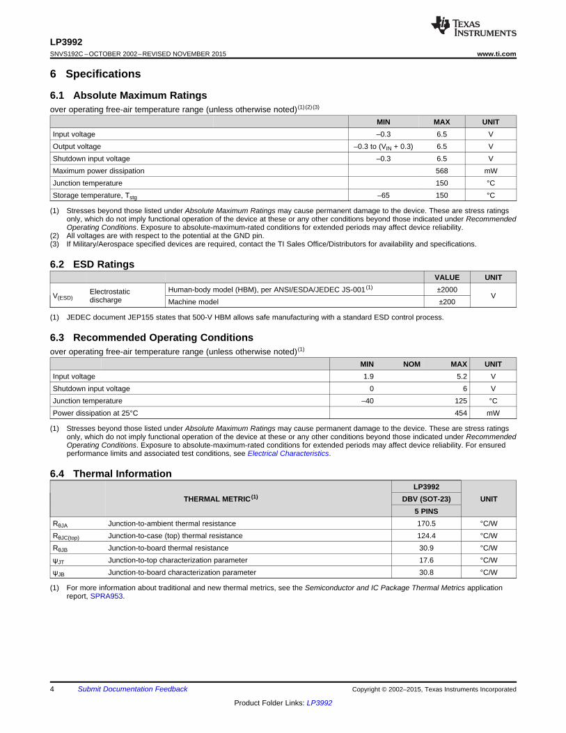
6 Specifications
6.1 Absolute Maximum Ratingsover operating free-air temperature range (unless otherwise noted) (1) (2) (3)
MIN MAX UNITInput voltage –0.3 6.5 VOutput voltage –0.3 to (VIN + 0.3) 6.5 VShutdown input voltage –0.3 6.5 VMaximum power dissipation 568 mWJunction temperature 150 °CStorage temperature, Tstg –65 150 °C
(1) Stresses beyond those listed under Absolute Maximum Ratings may cause permanent damage to the device. These are stress ratingsonly, which do not imply functional operation of the device at these or any other conditions beyond those indicated under RecommendedOperating Conditions. Exposure to absolute-maximum-rated conditions for extended periods may affect device reliability.
(2) All voltages are with respect to the potential at the GND pin.(3) If Military/Aerospace specified devices are required, contact the TI Sales Office/Distributors for availability and specifications.
6.2 ESD RatingsVALUE UNIT
Human-body model (HBM), per ANSI/ESDA/JEDEC JS-001 (1) ±2000ElectrostaticV(ESD) Vdischarge Machine model ±200
(1) JEDEC document JEP155 states that 500-V HBM allows safe manufacturing with a standard ESD control process.
6.3 Recommended Operating Conditionsover operating free-air temperature range (unless otherwise noted) (1)
MIN NOM MAX UNITInput voltage 1.9 5.2 VShutdown input voltage 0 6 VJunction temperature –40 125 °CPower dissipation at 25°C 454 mW
(1) Stresses beyond those listed under Absolute Maximum Ratings may cause permanent damage to the device. These are stress ratingsonly, which do not imply functional operation of the device at these or any other conditions beyond those indicated under RecommendedOperating Conditions. Exposure to absolute-maximum-rated conditions for extended periods may affect device reliability. For ensuredperformance limits and associated test conditions, see Electrical Characteristics.
6.4 Thermal InformationLP3992
THERMAL METRIC (1) DBV (SOT-23) UNIT5 PINS
RθJA Junction-to-ambient thermal resistance 170.5 °C/WRθJC(top) Junction-to-case (top) thermal resistance 124.4 °C/WRθJB Junction-to-board thermal resistance 30.9 °C/WψJT Junction-to-top characterization parameter 17.6 °C/WψJB Junction-to-board characterization parameter 30.8 °C/W
(1) For more information about traditional and new thermal metrics, see the Semiconductor and IC Package Thermal Metrics applicationreport, SPRA953.
4 Submit Documentation Feedback Copyright © 2002–2015, Texas Instruments Incorporated
Product Folder Links: LP3992

LP3992www.ti.com SNVS192C –OCTOBER 2002–REVISED NOVEMBER 2015
6.5 Electrical CharacteristicsUnless otherwise noted, VEN = 1.15, VIN = VOUT + 1 V, CIN = 1 µF, IOUT = 1 mA, COUT = 1 µF; typical values and limits apply forTJ = 25°C, and minimum and maximum limits apply over the full temperature range for operation, −40°C to +125°C. (1)
PARAMETER TEST CONDITIONS MIN TYP MAX UNITVIN Input voltage TJ = 25°C 1.9 5.2 mV
Output voltage tolerance Over full line and load regulation. –90 90 mVVIN = (VOUT(NOM) + 1 V) to 5.2 V,ΔVOUT Line regulation error –0.27 0.27 %/VIOUT = 1 mA
Load regulation error IOUT = 1 mA to 30 mA 100 220 µV/mAILOAD Load current See (2) and (3) 0 µA
VEN = 1.15 V, IOUT = 0 mA 26 50IQ Quiescent current VEN = 1.15 V, IOUT = 30 mA 29 50 µA
VEN = 0.4 V 0.003 1.5ISC Short-circuit current limit See (4) 90 mA
ƒ = 1 kHz, IOUT = 30 mA 40PSRR Power Supply Rejection Ratio dB
ƒ = 20 kHz, IOUT = 30 mA 30EEN Output noise voltage (3) BW = 10 Hz to 100 kHz, VIN = 4.2 V 300 µVRMS
Thermal shutdown temperature 160TSHUTDOWN °C
Thermal shutdown hysteresis 20ENABLE CONTROL CHARACTERISTICS
Maximum input current at ENIEN VEN = 0 V and VIN = 5.2 V 0.001 µAinputVIL Low input threshold VIN = 1.8 V to 5.2 V 0.4 VVIH High input threshold VIN = 1.8 V to 5.2 V 1.15 V
Line transient response |δVOUT| Trise = Tfall = 10 µS (3) 60Transient mVTrise = Tfall = 1 µSresponse Load transient response |δVOUT| 60IOUT = 100 µA to 5 mA (3)
(1) All limits are ensured. All electrical characteristics having room-temperature limits are tested during production at TJ = 25°C or correlatedusing Statistical Quality Control methods. Operation over the temperature specification is specified by correlating the electricalcharacteristics to process and temperature variations and applying statistical process control.
(2) The device maintains the regulated output voltage without the load.(3) This electrical specification is specified by design.(4) Short-circuit current is measured on the input supply line at the point when the short-circuit condition reduces the output voltage to 95%
of its nominal value.
6.6 Timing RequirementsMIN NOM MAX UNIT
tON1 Turnon time (1), 50% to 85% of VOUT(NOM)(2) 15 µs
tON2 Turnon time (1) to 95% level (3) 40 µstOFF1 Turnoff time (1), 85% to 50% of VOUT(NOM)
(4) µstOFF2 Turnoff time (1), 95% to 5% level (5) 40 15 µs
(1) This electrical specification is ensured by design.(2) Time for VOUT to rise from 50% to 85% of VOUT(NOM) (Figure 1).(3) Time from VEN = 1.15 V to VOUT = 95% (VOUT(NOM)) (Figure 1).(4) Time for VOUT to fall from 85% to 50% of VOUT(NOM) (Figure 1).(5) Time from VEN = 0.4 V to VOUT = 5% (VOUT(NOM) (Figure 1).
Copyright © 2002–2015, Texas Instruments Incorporated Submit Documentation Feedback 5
Product Folder Links: LP3992

LP3992SNVS192C –OCTOBER 2002–REVISED NOVEMBER 2015 www.ti.com
Figure 1. tON and tOFF Timing Diagram
6 Submit Documentation Feedback Copyright © 2002–2015, Texas Instruments Incorporated
Product Folder Links: LP3992
LP3992www.ti.com SNVS192C –OCTOBER 2002–REVISED NOVEMBER 2015
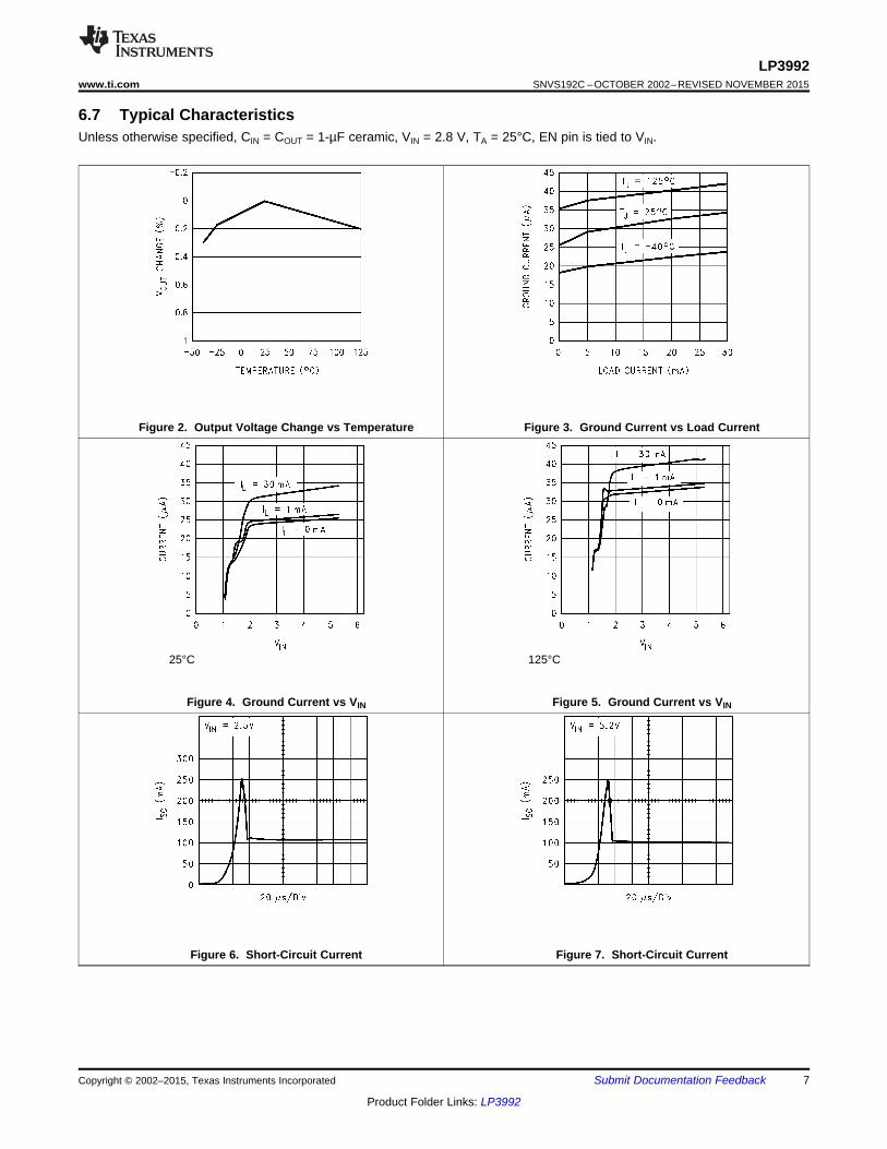
6.7 Typical CharacteristicsUnless otherwise specified, CIN = COUT = 1-µF ceramic, VIN = 2.8 V, TA = 25°C, EN pin is tied to VIN.
Figure 2. Output Voltage Change vs Temperature Figure 3. Ground Current vs Load Current
25°C 125°C
Figure 4. Ground Current vs VIN Figure 5. Ground Current vs VIN
Figure 6. Short-Circuit Current Figure 7. Short-Circuit Current
Copyright © 2002–2015, Texas Instruments Incorporated Submit Documentation Feedback 7
Product Folder Links: LP3992
LP3992SNVS192C –OCTOBER 2002–REVISED NOVEMBER 2015 www.ti.com
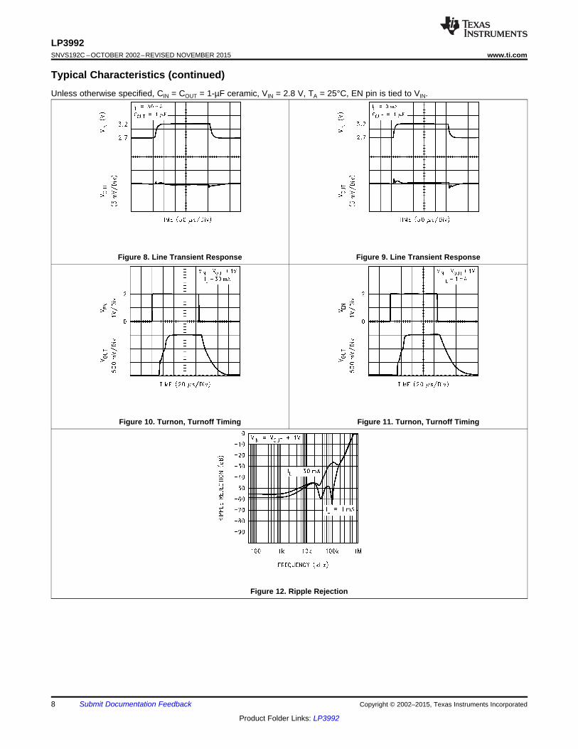
Typical Characteristics (continued)Unless otherwise specified, CIN = COUT = 1-µF ceramic, VIN = 2.8 V, TA = 25°C, EN pin is tied to VIN.
Figure 8. Line Transient Response Figure 9. Line Transient Response
Figure 10. Turnon, Turnoff Timing Figure 11. Turnon, Turnoff Timing
Figure 12. Ripple Rejection
8 Submit Documentation Feedback Copyright © 2002–2015, Texas Instruments Incorporated
Product Folder Links: LP3992
LP3992www.ti.com SNVS192C –OCTOBER 2002–REVISED NOVEMBER 2015
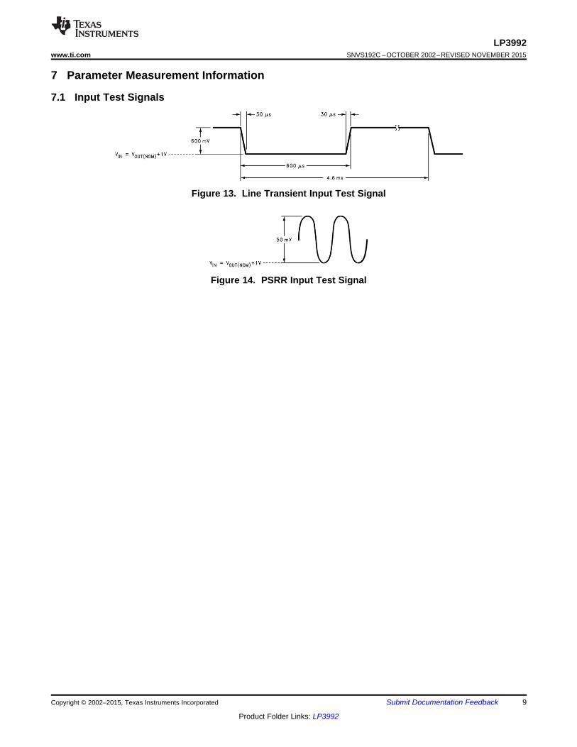
7 Parameter Measurement Information
7.1 Input Test Signals
Figure 13. Line Transient Input Test Signal
Figure 14. PSRR Input Test Signal
Copyright © 2002–2015, Texas Instruments Incorporated Submit Documentation Feedback 9
Product Folder Links: LP3992

IN
VBG
+
GND
OUT
VIH
+
CAP
LP3992
HI = ONLOW = OFF
Fast Turnoff
Current LimitThermal Limit
SDEN
LP3992SNVS192C –OCTOBER 2002–REVISED NOVEMBER 2015 www.ti.com
8 Detailed Description
8.1 OverviewThe LP3992 device is a CMOS voltage regulator with a low-input operating-voltage tolerance. Key protectioncircuits, including thermal-overload and short-circuit protection, are integrated in the device. Using the EN pin,the device may be controlled to provide a SHUTDOWN state, in which negligible supply current is drawn. TheLP3992 is designed to be stable with space-saving ceramic capacitors.
8.2 Functional Block Diagram
10 Submit Documentation Feedback Copyright © 2002–2015, Texas Instruments Incorporated
Product Folder Links: LP3992
LP3992www.ti.com SNVS192C –OCTOBER 2002–REVISED NOVEMBER 2015
8.3 Feature Description
8.3.1 Shutdown and EnableThe LP3992 may be switched ON or OFF by a logic input at the EN pin. A high voltage at the EN pin turns thedevice on. A low voltage on the EN pin will disable the regulator, and will activate the fast turnoff circuitry todischarge the output capacitance. When the regulator is disabled the device typically consumes 3 nA.
If the application does not require the EN feature, the EN pin must be tied to VIN to keep the regulator outputpermanently on.
To ensure proper operation, the signal source used to drive the EN input must be able to swing above and belowthe specified turnon or turnoff voltage thresholds listed in the Electrical Characteristics under VIL and VIH.
8.3.2 Fast Turnon and TurnoffThe controlled shutdown feature of the device provides a fast turn off by discharging the output capacitor via aninternal FET device. This discharge is current limited by the RDSON of this switch. Fast turnon is ensured bycontrol circuitry within the reference block allowing a very fast ramp of the output voltage to reach the targetvoltage.
8.4 Device Functional Modes
8.4.1 Enable OperationThe LP3992 may be switched ON or OFF by a logic input at the EN pin. A high voltage at the EN pin turns thedevice on. A low voltage on the EN pin will disable the regulator, and will activate the fast turnoff circuitry todischarge the output capacitance. When the regulator is disabled the device typically consumes 3 nA.
If the application does not require the EN feature, the EN pin should be tied to VIN to keep the regulator outputpermanently on.
To ensure proper operation, the signal source used to drive the EN input must be able to swing above and belowthe specified turnon or turnoff voltage thresholds listed in the Electrical Characteristics under VIL and VIH.
Copyright © 2002–2015, Texas Instruments Incorporated Submit Documentation Feedback 11
Product Folder Links: LP3992

LP3992
EN
OUT
GND
CAP
INVIN
VEN
VOUT
1 PF
1 PF
COUT
CIN
High= ONLow= OFF
LP3992SNVS192C –OCTOBER 2002–REVISED NOVEMBER 2015 www.ti.com
9 Application And Implementation
NOTEInformation in the following applications sections is not part of the TI componentspecification, and TI does not warrant its accuracy or completeness. TI’s customers areresponsible for determining suitability of components for their purposes. Customers shouldvalidate and test their design implementation to confirm system functionality.
9.1 Application InformationThe LP3992 can provide 30-mA output current with 1.9-V to 5.2-V input. It is stable with 1-μF ceramic input andoutput capacitors. Typical output noise is 300 μVRMS at frequencies from 10 Hz to 100 kHz. Typical power supplyrejection is 40 dB at 1 kHz.
9.2 Typical Application
Figure 15. LP3992 Typical Application
9.2.1 Design RequirementsFor typical CMOS voltage regulator applications, use the parameters listed in Table 1.
Table 1. Design ParametersDESIGN PARAMETER EXAMPLE VALUEMinimum input voltage 1.9 V
Output voltage 1.5 ± 0.09 VOutput current 30 mA
9.2.2 Detailed Design Procedure
9.2.2.1 External CapacitorsIn common with most regulators, the LP3992 requires external capacitors for regulator stability. The device isspecifically designed for portable applications requiring minimum board space and smallest components. Thesecapacitors must be correctly selected for good performance.
12 Submit Documentation Feedback Copyright © 2002–2015, Texas Instruments Incorporated
Product Folder Links: LP3992

LP3992www.ti.com SNVS192C –OCTOBER 2002–REVISED NOVEMBER 2015
9.2.2.2 Input CapacitorAn input capacitor is required for stability. It is recommended that a 1-µF capacitor be connected between theLP3992 IN pin and ground (this capacitance value may be increased without limit).
This capacitor must be located a distance of not more than 1 cm from the IN pin and returned to a clean analogground. Any good-quality ceramic, tantalum, or film capacitor may be used at the input.
NOTETantalum capacitors can suffer catastrophic failures due to surge current when connectedto a low-impedance source of power (like a battery or a very large capacitor). If a tantalumcapacitor is used at the input, it must be ensured by the manufacturer to have a surgecurrent rating sufficient for the application.
There are no requirements for the equivalent series resistance (ESR) on the input capacitor, but tolerance andtemperature coefficient must be considered when selecting the capacitor to ensure the capacitance will remain ≊1 µF over the entire operating temperature range.
9.2.2.3 Output CapacitorThe LP3992 is designed specifically to work with very small ceramic output capacitors. A 1-µF ceramic capacitor(dielectric types Z5U, Y5V or X7R) with ESR from 5 mΩ to 500 mΩ, is suitable in the LP3992 application circuit.
For this device the output capacitor should be connected between the CAP pin and ground. It is also possible toconnect the output capacitor directly to the OUT pin. In this case the CAP pin must be left open-circuit or tieddirectly to the OUT pin.
Tantalum or film capacitors may also be used at the device output, CAP (or OUT), but these are not as attractivefor reasons of size and cost (see Capacitor Characteristics).
The output capacitor must meet the requirement for the minimum value of capacitance and also have an ESRvalue that is within the 5-mΩ to 500-mΩ range for stability.
Table 2. Recommended Output CapacitorPARAMETER TEST CONDITIONS MIN TYP MAX UNIT
Capacitance (1) 0.7 1 µFCOUT Output capacitor
ESR 5 500 mΩ
(1) The capacitor tolerance should be ±30% or better over the temperature range. The recommended capacitor type is X7R however,dependant on the application X5R, Y5V, and Z5U can also be used.
9.2.2.4 No-Load StabilityThe LP3992 will remain stable and in regulation with no external load. This is an important consideration in somecircuits, for example CMOS RAM keep-alive applications.
9.2.2.5 Capacitor CharacteristicsThe LP3992 is designed to work with ceramic capacitors on the output to take advantage of the benefits theyoffer. For capacitance values in the 1-µF to 4.7-µF range, ceramic capacitors are the smallest, least expensive,and have the lowest ESR values, thus making them best for eliminating high frequency noise. The ESR of atypical 1-µF ceramic capacitor is in the 20-mΩ to 40-mΩ range that easily meets the ESR requirement forstability for the LP3992.
The temperature performance of ceramic capacitors varies by type. Most large-value ceramic capacitors(≥ 2.2 µF) are manufactured with Z5U or Y5V temperature characteristics, which results in the capacitancedropping by more than 50% as the temperature goes from 25°C to 85°C.
A better choice for temperature coefficient in a ceramic capacitor is X7R. This type of capacitor is the most stableand holds the capacitance within ±15% over the temperature range.
Tantalum capacitors are less desirable than ceramic for use as output capacitors because they are moreexpensive when comparing equivalent capacitance and voltage ratings in the 1-µF to 4.7-µF range.
Copyright © 2002–2015, Texas Instruments Incorporated Submit Documentation Feedback 13
Product Folder Links: LP3992

LP3992SNVS192C –OCTOBER 2002–REVISED NOVEMBER 2015 www.ti.com
Another important consideration is that tantalum capacitors have higher ESR values than equivalent sizeceramics. This means that while it may be possible to find a tantalum capacitor with an ESR value within thestable range, it would have to be larger in capacitance (which means bigger and more costly) than a ceramiccapacitor with the same ESR value. Also, the ESR of a typical tantalum increases about 2:1 as the temperaturegoes from 25°C down to –40°C, so some guard band must be allowed.
9.2.2.6 Power DissipationThe permissible power dissipation for any package is a measure of the capability of the device to pass heat fromthe power source, the junctions of the device, to the ultimate heat sink, the ambient environment. Thus, thepower dissipation is dependent on the ambient temperature and the thermal resistance across the variousinterfaces between the die and ambient air (see Equation 1).
TA(MAX) = TJ(MAX-OP) − (PD(MAX) × RθJA) (1)
The allowable power dissipation for the device in a given package can be calculated:PD = TJ(MAX) – TA / RθJA (2)
The actual power dissipation across the device can be represented by Equation 3:PD = (VIN − VOUT) × IOUT (3)
This establishes the relationship between the power dissipation allowed due to thermal consideration, the voltagedrop across the device, and the continuous current capability of the device. Equation 2 and Equation 3 must beused to determine the optimum operating conditions for the device in the application.
This thermal resistance (RθJA) is highly dependent on the heat-spreading capability of the particular PCB designand therefore varies according to the total copper area, copper weight, and location of the planes. The RθJArecorded in Thermal Information is determined by the specific EIA/JEDEC JESD51-7 standard for PCB andcopper-spreading area and is to be used only as a relative measure of package thermal performance. For a well-designed thermal layout, RθJA is actually the sum of the SOT-23 package junction-to-board thermal resistance(RθJB) plus the thermal resistance contribution by the PCB copper area acting as a heatsink.
9.2.2.7 Estimating Junction TemperatureThe EIA/JEDEC standard recommends the use of psi (Ψ) thermal characteristics to estimate the junctiontemperatures of surface mount devices on a typical PCB board application. These characteristics are not truethermal resistance values, but rather package specific thermal characteristics that offer practical and relativemeans of estimating junction temperatures. These psi metrics are determined to be significantly independent ofcopper-spreading area. The key thermal characteristics (ΨJT and ΨJB) are given in Thermal Information and areused in accordance with Equation 4 or Equation 5.
TJ(MAX) = TTOP + (ΨJT × PD(MAX))
where• PD(MAX) is explained in Equation 2• TTOP is the temperature measured at the center-top of the device package. (4)
TJ(MAX) = TBOARD + (ΨJB × PD(MAX))
where• PD(MAX) is explained in Equation 2.• TBOARD is the PCB surface temperature measured 1-mm from the device package and centered on the
package edge. (5)
For more information about the thermal characteristics ΨJT and ΨJB, see TI Application Report Semiconductorand IC Package Thermal Metrics (SPRA953); for more information about measuring TTOP and TBOARD, see the TIApplication Report Using New Thermal Metrics (SBVA025); and for more information about the EIA/JEDECJESD51 PCB used for validating RθJA, see the TI Application Report Thermal Characteristics of Linear and LogicPackages Using JEDEC PCB Designs (SZZA017). Aforementioned application notes are available atwww.ti.com.
14 Submit Documentation Feedback Copyright © 2002–2015, Texas Instruments Incorporated
Product Folder Links: LP3992
IN
GND
OUT
CAP
CIN
COUT2
VIN
GND
VEN
VOUT
GND
4
5
3
1
EN
LP3992www.ti.com SNVS192C –OCTOBER 2002–REVISED NOVEMBER 2015
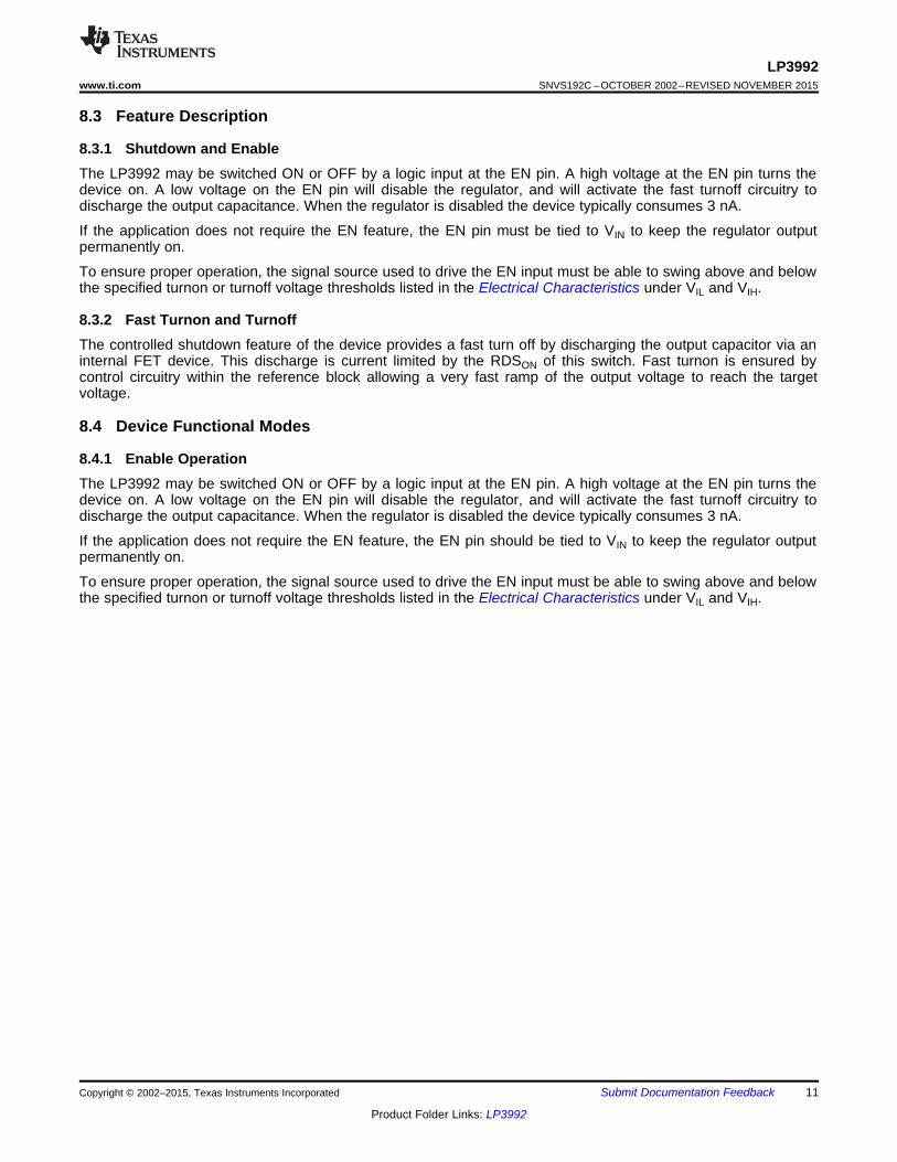
9.2.3 Application Curves
Figure 16. Load Transient Response Figure 17. Load Transient Response
10 Power Supply RecommendationsThe LP3992 is designed to operate from an input voltage supply range from 1.9 V to 5.2 V.
11 Layout
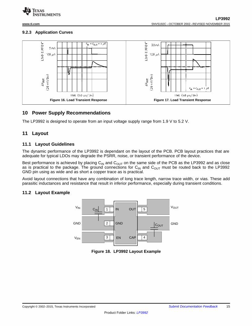
11.1 Layout GuidelinesThe dynamic performance of the LP3992 is dependant on the layout of the PCB. PCB layout practices that areadequate for typical LDOs may degrade the PSRR, noise, or transient performance of the device.
Best performance is achieved by placing CIN and COUT on the same side of the PCB as the LP3992 and as closeas is practical to the package. The ground connections for CIN and COUT must be routed back to the LP3992GND pin using as wide and as short a copper trace as is practical.
Avoid layout connections that have any combination of long trace length, narrow trace width, or vias. These addparasitic inductances and resistance that result in inferior performance, especially during transient conditions.
11.2 Layout Example
Figure 18. LP3992 Layout Example
Copyright © 2002–2015, Texas Instruments Incorporated Submit Documentation Feedback 15
Product Folder Links: LP3992

LP3992SNVS192C –OCTOBER 2002–REVISED NOVEMBER 2015 www.ti.com
12 Device and Documentation Support
12.1 Documentation Support
12.1.1 Related DocumentationFor related documentation see the following:• TI Application Report Semiconductor and IC Package Thermal Metrics (SPRA953)• TI Application Report Using New Thermal Metrics (SBVA025)• TI Application Report Thermal Characteristics of Linear and Logic Packages Using JEDEC PCB Designs
(SZZA017)
12.2 Community ResourcesThe following links connect to TI community resources. Linked contents are provided "AS IS" by the respectivecontributors. They do not constitute TI specifications and do not necessarily reflect TI's views; see TI's Terms ofUse.
TI E2E™ Online Community TI's Engineer-to-Engineer (E2E) Community. Created to foster collaborationamong engineers. At e2e.ti.com, you can ask questions, share knowledge, explore ideas and helpsolve problems with fellow engineers.
Design Support TI's Design Support Quickly find helpful E2E forums along with design support tools andcontact information for technical support.
12.3 TrademarksE2E is a trademark of Texas Instruments.All other trademarks are the property of their respective owners.
12.4 Electrostatic Discharge CautionThese devices have limited built-in ESD protection. The leads should be shorted together or the device placed in conductive foamduring storage or handling to prevent electrostatic damage to the MOS gates.
12.5 GlossarySLYZ022 — TI Glossary.
This glossary lists and explains terms, acronyms, and definitions.
13 Mechanical, Packaging, and Orderable InformationThe following pages include mechanical, packaging, and orderable information. This information is the mostcurrent data available for the designated devices. This data is subject to change without notice and revision ofthis document. For browser-based versions of this data sheet, refer to the left-hand navigation.
16 Submit Documentation Feedback Copyright © 2002–2015, Texas Instruments Incorporated
Product Folder Links: LP3992

PACKAGE OPTION ADDENDUM
www.ti.com 3-Nov-2015
Addendum-Page 1
PACKAGING INFORMATION
Orderable Device Status(1)
Package Type PackageDrawing
Pins PackageQty
Eco Plan(2)
Lead/Ball Finish(6)
MSL Peak Temp(3)
Op Temp (°C) Device Marking(4/5)
Samples
LP3992IMFX-1.5/NOPB ACTIVE SOT-23 DBV 5 3000 Green (RoHS& no Sb/Br)
CU SN Level-1-260C-UNLIM -40 to 125 LFHB
(1) The marketing status values are defined as follows:ACTIVE: Product device recommended for new designs.LIFEBUY: TI has announced that the device will be discontinued, and a lifetime-buy period is in effect.NRND: Not recommended for new designs. Device is in production to support existing customers, but TI does not recommend using this part in a new design.PREVIEW: Device has been announced but is not in production. Samples may or may not be available.OBSOLETE: TI has discontinued the production of the device.
(2) Eco Plan - The planned eco-friendly classification: Pb-Free (RoHS), Pb-Free (RoHS Exempt), or Green (RoHS & no Sb/Br) - please check http://www.ti.com/productcontent for the latest availabilityinformation and additional product content details.TBD: The Pb-Free/Green conversion plan has not been defined.Pb-Free (RoHS): TI's terms "Lead-Free" or "Pb-Free" mean semiconductor products that are compatible with the current RoHS requirements for all 6 substances, including the requirement thatlead not exceed 0.1% by weight in homogeneous materials. Where designed to be soldered at high temperatures, TI Pb-Free products are suitable for use in specified lead-free processes.Pb-Free (RoHS Exempt): This component has a RoHS exemption for either 1) lead-based flip-chip solder bumps used between the die and package, or 2) lead-based die adhesive used betweenthe die and leadframe. The component is otherwise considered Pb-Free (RoHS compatible) as defined above.Green (RoHS & no Sb/Br): TI defines "Green" to mean Pb-Free (RoHS compatible), and free of Bromine (Br) and Antimony (Sb) based flame retardants (Br or Sb do not exceed 0.1% by weightin homogeneous material)
(3) MSL, Peak Temp. - The Moisture Sensitivity Level rating according to the JEDEC industry standard classifications, and peak solder temperature.
(4) There may be additional marking, which relates to the logo, the lot trace code information, or the environmental category on the device.
(5) Multiple Device Markings will be inside parentheses. Only one Device Marking contained in parentheses and separated by a "~" will appear on a device. If a line is indented then it is a continuationof the previous line and the two combined represent the entire Device Marking for that device.
(6) Lead/Ball Finish - Orderable Devices may have multiple material finish options. Finish options are separated by a vertical ruled line. Lead/Ball Finish values may wrap to two lines if the finishvalue exceeds the maximum column width.
Important Information and Disclaimer:The information provided on this page represents TI's knowledge and belief as of the date that it is provided. TI bases its knowledge and belief on informationprovided by third parties, and makes no representation or warranty as to the accuracy of such information. Efforts are underway to better integrate information from third parties. TI has taken andcontinues to take reasonable steps to provide representative and accurate information but may not have conducted destructive testing or chemical analysis on incoming materials and chemicals.TI and TI suppliers consider certain information to be proprietary, and thus CAS numbers and other limited information may not be available for release.
In no event shall TI's liability arising out of such information exceed the total purchase price of the TI part(s) at issue in this document sold by TI to Customer on an annual basis.

PACKAGE OPTION ADDENDUM
www.ti.com 3-Nov-2015
Addendum-Page 2
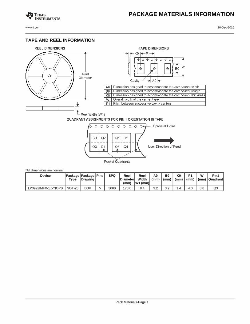
TAPE AND REEL INFORMATION
*All dimensions are nominal
Device PackageType
PackageDrawing
Pins SPQ ReelDiameter
(mm)
ReelWidth
W1 (mm)
A0(mm)
B0(mm)
K0(mm)
P1(mm)
W(mm)
Pin1Quadrant
LP3992IMFX-1.5/NOPB SOT-23 DBV 5 3000 178.0 8.4 3.2 3.2 1.4 4.0 8.0 Q3
PACKAGE MATERIALS INFORMATION
www.ti.com 20-Dec-2016
Pack Materials-Page 1
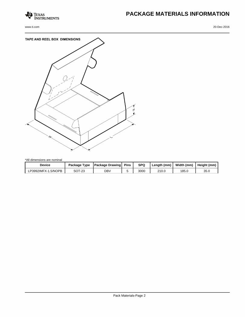
*All dimensions are nominal
Device Package Type Package Drawing Pins SPQ Length (mm) Width (mm) Height (mm)
LP3992IMFX-1.5/NOPB SOT-23 DBV 5 3000 210.0 185.0 35.0
PACKAGE MATERIALS INFORMATION
www.ti.com 20-Dec-2016
Pack Materials-Page 2


www.ti.com
PACKAGE OUTLINE
C
TYP0.220.08
0.25
3.02.6
2X 0.95
1.9
1.45 MAX
TYP0.150.00
5X 0.50.3
TYP0.60.3
TYP80
1.9
A
3.052.75
B1.751.45
(1.1)
SOT-23 - 1.45 mm max heightDBV0005ASMALL OUTLINE TRANSISTOR
4214839/C 04/2017
NOTES: 1. All linear dimensions are in millimeters. Any dimensions in parenthesis are for reference only. Dimensioning and tolerancing per ASME Y14.5M.2. This drawing is subject to change without notice.3. Refernce JEDEC MO-178.
0.2 C A B
1
34
5
2
INDEX AREAPIN 1
GAGE PLANE
SEATING PLANE
0.1 C
SCALE 4.000
www.ti.com
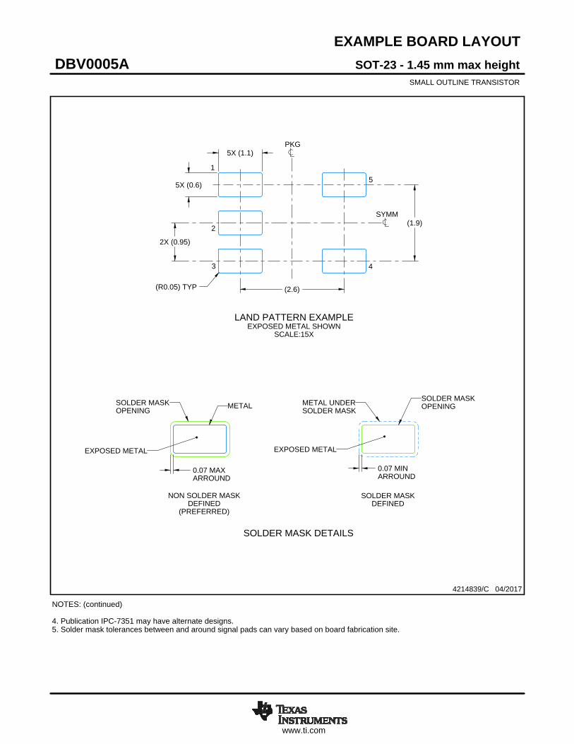
EXAMPLE BOARD LAYOUT
0.07 MAXARROUND
0.07 MINARROUND
5X (1.1)
5X (0.6)
(2.6)
(1.9)
2X (0.95)
(R0.05) TYP
4214839/C 04/2017
SOT-23 - 1.45 mm max heightDBV0005ASMALL OUTLINE TRANSISTOR
NOTES: (continued) 4. Publication IPC-7351 may have alternate designs. 5. Solder mask tolerances between and around signal pads can vary based on board fabrication site.
SYMM
LAND PATTERN EXAMPLEEXPOSED METAL SHOWN
SCALE:15X
PKG
1
3 4
5
2
SOLDER MASKOPENINGMETAL UNDER
SOLDER MASK
SOLDER MASKDEFINED
EXPOSED METAL
METALSOLDER MASKOPENING
NON SOLDER MASKDEFINED
(PREFERRED)
SOLDER MASK DETAILS
EXPOSED METAL

www.ti.com
EXAMPLE STENCIL DESIGN
(2.6)
(1.9)
2X(0.95)
5X (1.1)
5X (0.6)
(R0.05) TYP
SOT-23 - 1.45 mm max heightDBV0005ASMALL OUTLINE TRANSISTOR
4214839/C 04/2017
NOTES: (continued) 6. Laser cutting apertures with trapezoidal walls and rounded corners may offer better paste release. IPC-7525 may have alternate design recommendations. 7. Board assembly site may have different recommendations for stencil design.
SOLDER PASTE EXAMPLEBASED ON 0.125 mm THICK STENCIL
SCALE:15X
SYMM
PKG
1
3 4
5
2
IMPORTANT NOTICE
Texas Instruments Incorporated (TI) reserves the right to make corrections, enhancements, improvements and other changes to itssemiconductor products and services per JESD46, latest issue, and to discontinue any product or service per JESD48, latest issue. Buyersshould obtain the latest relevant information before placing orders and should verify that such information is current and complete.TI’s published terms of sale for semiconductor products (http://www.ti.com/sc/docs/stdterms.htm) apply to the sale of packaged integratedcircuit products that TI has qualified and released to market. Additional terms may apply to the use or sale of other types of TI products andservices.Reproduction of significant portions of TI information in TI data sheets is permissible only if reproduction is without alteration and isaccompanied by all associated warranties, conditions, limitations, and notices. TI is not responsible or liable for such reproduceddocumentation. Information of third parties may be subject to additional restrictions. Resale of TI products or services with statementsdifferent from or beyond the parameters stated by TI for that product or service voids all express and any implied warranties for theassociated TI product or service and is an unfair and deceptive business practice. TI is not responsible or liable for any such statements.Buyers and others who are developing systems that incorporate TI products (collectively, “Designers”) understand and agree that Designersremain responsible for using their independent analysis, evaluation and judgment in designing their applications and that Designers havefull and exclusive responsibility to assure the safety of Designers' applications and compliance of their applications (and of all TI productsused in or for Designers’ applications) with all applicable regulations, laws and other applicable requirements. Designer represents that, withrespect to their applications, Designer has all the necessary expertise to create and implement safeguards that (1) anticipate dangerousconsequences of failures, (2) monitor failures and their consequences, and (3) lessen the likelihood of failures that might cause harm andtake appropriate actions. Designer agrees that prior to using or distributing any applications that include TI products, Designer willthoroughly test such applications and the functionality of such TI products as used in such applications.TI’s provision of technical, application or other design advice, quality characterization, reliability data or other services or information,including, but not limited to, reference designs and materials relating to evaluation modules, (collectively, “TI Resources”) are intended toassist designers who are developing applications that incorporate TI products; by downloading, accessing or using TI Resources in anyway, Designer (individually or, if Designer is acting on behalf of a company, Designer’s company) agrees to use any particular TI Resourcesolely for this purpose and subject to the terms of this Notice.TI’s provision of TI Resources does not expand or otherwise alter TI’s applicable published warranties or warranty disclaimers for TIproducts, and no additional obligations or liabilities arise from TI providing such TI Resources. TI reserves the right to make corrections,enhancements, improvements and other changes to its TI Resources. TI has not conducted any testing other than that specificallydescribed in the published documentation for a particular TI Resource.Designer is authorized to use, copy and modify any individual TI Resource only in connection with the development of applications thatinclude the TI product(s) identified in such TI Resource. NO OTHER LICENSE, EXPRESS OR IMPLIED, BY ESTOPPEL OR OTHERWISETO ANY OTHER TI INTELLECTUAL PROPERTY RIGHT, AND NO LICENSE TO ANY TECHNOLOGY OR INTELLECTUAL PROPERTYRIGHT OF TI OR ANY THIRD PARTY IS GRANTED HEREIN, including but not limited to any patent right, copyright, mask work right, orother intellectual property right relating to any combination, machine, or process in which TI products or services are used. Informationregarding or referencing third-party products or services does not constitute a license to use such products or services, or a warranty orendorsement thereof. Use of TI Resources may require a license from a third party under the patents or other intellectual property of thethird party, or a license from TI under the patents or other intellectual property of TI.TI RESOURCES ARE PROVIDED “AS IS” AND WITH ALL FAULTS. TI DISCLAIMS ALL OTHER WARRANTIES ORREPRESENTATIONS, EXPRESS OR IMPLIED, REGARDING RESOURCES OR USE THEREOF, INCLUDING BUT NOT LIMITED TOACCURACY OR COMPLETENESS, TITLE, ANY EPIDEMIC FAILURE WARRANTY AND ANY IMPLIED WARRANTIES OFMERCHANTABILITY, FITNESS FOR A PARTICULAR PURPOSE, AND NON-INFRINGEMENT OF ANY THIRD PARTY INTELLECTUALPROPERTY RIGHTS. TI SHALL NOT BE LIABLE FOR AND SHALL NOT DEFEND OR INDEMNIFY DESIGNER AGAINST ANY CLAIM,INCLUDING BUT NOT LIMITED TO ANY INFRINGEMENT CLAIM THAT RELATES TO OR IS BASED ON ANY COMBINATION OFPRODUCTS EVEN IF DESCRIBED IN TI RESOURCES OR OTHERWISE. IN NO EVENT SHALL TI BE LIABLE FOR ANY ACTUAL,DIRECT, SPECIAL, COLLATERAL, INDIRECT, PUNITIVE, INCIDENTAL, CONSEQUENTIAL OR EXEMPLARY DAMAGES INCONNECTION WITH OR ARISING OUT OF TI RESOURCES OR USE THEREOF, AND REGARDLESS OF WHETHER TI HAS BEENADVISED OF THE POSSIBILITY OF SUCH DAMAGES.Unless TI has explicitly designated an individual product as meeting the requirements of a particular industry standard (e.g., ISO/TS 16949and ISO 26262), TI is not responsible for any failure to meet such industry standard requirements.Where TI specifically promotes products as facilitating functional safety or as compliant with industry functional safety standards, suchproducts are intended to help enable customers to design and create their own applications that meet applicable functional safety standardsand requirements. Using products in an application does not by itself establish any safety features in the application. Designers mustensure compliance with safety-related requirements and standards applicable to their applications. Designer may not use any TI products inlife-critical medical equipment unless authorized officers of the parties have executed a special contract specifically governing such use.Life-critical medical equipment is medical equipment where failure of such equipment would cause serious bodily injury or death (e.g., lifesupport, pacemakers, defibrillators, heart pumps, neurostimulators, and implantables). Such equipment includes, without limitation, allmedical devices identified by the U.S. Food and Drug Administration as Class III devices and equivalent classifications outside the U.S.TI may expressly designate certain products as completing a particular qualification (e.g., Q100, Military Grade, or Enhanced Product).Designers agree that it has the necessary expertise to select the product with the appropriate qualification designation for their applicationsand that proper product selection is at Designers’ own risk. Designers are solely responsible for compliance with all legal and regulatoryrequirements in connection with such selection.Designer will fully indemnify TI and its representatives against any damages, costs, losses, and/or liabilities arising out of Designer’s non-compliance with the terms and provisions of this Notice.
Mailing Address: Texas Instruments, Post Office Box 655303, Dallas, Texas 75265Copyright © 2018, Texas Instruments Incorporated