lt6375 - ±270v common mode voltage difference amplifier · ±270v common mode voltage difference...
TRANSCRIPT

LT6375
16375fa
For more information www.linear.com/LT6375
TYPICAL APPLICATION
FEATURES DESCRIPTION
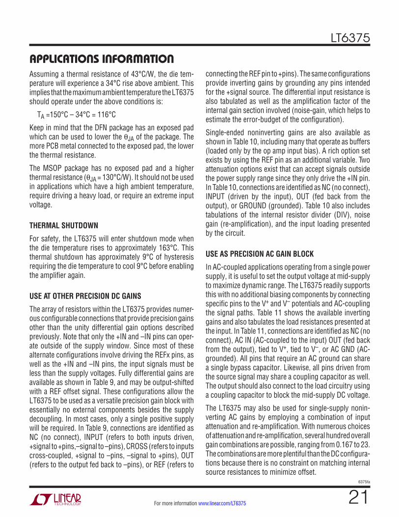
±270V Common Mode Voltage Difference Amplifier
The LT®6375 is a unity-gain difference amplifier which combines excellent DC precision, a very high input common mode range and a wide supply voltage range. It includes a precision op amp and a highly-matched thin film resistor network. It features excellent CMRR, extremely low gain error and extremely low gain drift.
Comparing the LT6375 to existing difference amplifiers with high common mode voltage range, the selectable resistor divider ratios of the LT6375 offer superior system performance by allowing the user to achieve maximum SNR, precision and speed for a specific input common mode voltage range.
The op amp at the core of the LT6375 has Over-The-Top® protected inputs which allow for robust operation in envi-ronments with unpredictable voltage conditions. See the Applications Information section for more details.
The LT6375 is specified over the –40°C to 125°C tem-perature range and is available in space-saving MSOP16 and DFN14 packages.
Precision Wide Voltage Range, Bidirectional Current Monitor
APPLICATIONS n High Side or Low Side Current Sensing n Bidirectional Wide Common Mode Range Current Sensing n High Voltage to Low Voltage Level Translation n Precision Difference Amplifier n Industrial Data-Acquisition Front-Ends n Replacement for Isolation Circuits
L, LT, LTC, LTM, Linear Technology, Over-The-Top and the Linear logo are registered trademarks of Linear Technology Corporation. All other trademarks are the property of their respective owners.
n ±270V Common Mode Voltage Range n 97dB Minimum CMRR (LT6375A) n 0.0035% (35ppm) Maximum Gain Error (LT6375A) n 1ppm/°C Maximum Gain Error Drift n 2ppm Maximum Gain Nonlinearity n Wide Supply Voltage Range: 3.3V to 50V n Rail-to-Rail Output n 350µA Supply Current n Selectable Internal Resistor Divider Ratio n 300µV Maximum Offset Voltage (LT6375A) n 575kHz –3dB Bandwidth (Resistor Divider = 7) n 375kHz –3dB Bandwidth (Resistor Divider = 20) n –40°C to 125°C Specified Temperature Range n Low Power Shutdown: 20μA (DFN Package Only) n Space-Saving MSOP and DFN Packages
CMRR (µV/V = ppm)–40 –30 –20 –10 0 10 20 30 40
0
20
40
60
80
100
120
140
160
180
200
NUM
BER
OF U
NITS
6375 TA01b
1248 UNITSFROM 4 RUNS
VS = ±15VVIN = ±270VDIV = 25
Typical Distribution of CMRR
–
+
V+
V–
–15V
VSOURCE+ = –270V TO 270V
15V
OUT VOUT = ±10mV/mA
REF
–REFA
–IN
+IN
–REFB
19k 38k
190k
190k
190k
23.75k
–REFC
+REFA +REFB +REFC6375 TA01a
19k 38k
SHDN
23.75k
RC10Ω
RSENSE10Ω
190k
LOAD
LT6375
26375fa
For more information www.linear.com/LT6375
PIN CONFIGURATION
ABSOLUTE MAXIMUM RATINGS
Supply Voltages (V+ to V–) ..............................................................60V+IN, –IN, (Note 2) Each Input .........................................................±270V Differential ........................................................±540V+REFA, –REFA, +REFB, –REFB, +REFC, –REFC, REF, SHDN (Note 2) ................ (V+ + 0.3V) to (V– –0.3V)Output Current (Continuous) (Note 6) ....................50mA
1
3
4
5
6
7
+IN
+REFA
+REFB
+REFC
REF
SHDN
–IN
–REFA
–REFB
–REFC
V+
OUT
15 V–
14
12
11
10
9
8
TOP VIEW
DF PACKAGE14(12)-LEAD (4mm × 4mm) PLASTIC DFN TJMAX = 150°C, θJA = 43°C/W, θJC = 4°C/W
EXPOSED PAD (PIN 15) IS V–, MUST BE SOLDERED TO PCB
1
3
5678
+IN
+REFA
+REFB+REFC
REFV–
16
14
1211109
–IN
–REFA
–REFB–REFCV+
OUT
TOP VIEW
MS PACKAGEVARIATION: MS16 (12)
16-LEAD PLASTIC MSOP TJMAX = 150°C, θJA = 130°C/W
ORDER INFORMATIONLEAD FREE FINISH TAPE AND REEL PART MARKING* PACKAGE DESCRIPTION TEMPERATURE RANGE
LT6375IDF#PBF LT6375IDF#TRPBF 6375 14-Lead (4mm × 4mm) Plastic DFN –40°C to 85°C
LT6375HDF#PBF LT6375HDF#TRPBF 6375 14-Lead (4mm × 4mm) Plastic DFN –40°C to 125°C
LT6375AHDF#PBF LT6375AHDF#TRPBF 6375 14-Lead (4mm × 4mm) Plastic DFN –40°C to 125°C
LT6375IMS#PBF LT6375IMS#TRPBF 6375 16-Lead Plastic MSOP –40°C to 85°C
LT6375HMS#PBF LT6375HMS#TRPBF 6375 16-Lead Plastic MSOP –40°C to 125°C
LT6375AHMS#PBF LT6375AHMS#TRPBF 6375 16-Lead Plastic MSOP –40°C to 125°C
Consult LTC Marketing for parts specified with wider operating temperature ranges. *The temperature grade is identified by a label on the shipping container.For more information on lead free part marking, go to: http://www.linear.com/leadfree/ For more information on tape and reel specifications, go to: http://www.linear.com/tapeandreel/. Some packages are available in 500 unit reels through designated sales channels with #TRMPBF suffix.
Output Short-Circuit Duration (Note 3) Thermally Limited Temperature Range (Notes 4, 5) LT6375I................................................–40°C to 85°C LT6375H ............................................ –40°C to 125°CStorage Temperature Range .................. –65°C to 150°CMSOP Lead Temperature (Soldering, 10 sec) ........ 300°C
(Note 1)
LT6375
36375fa
For more information www.linear.com/LT6375
ELECTRICAL CHARACTERISTICS The l denotes the specifications which apply over the full operating temperature range, –40°C < TA < 85°C for I-grade parts, –40°C < TA < 125°C for H-grade parts, otherwise specifications are at TA = 25°C, V+ = 15V, V– = –15V, VCM = VOUT = VREF = 0V. VCMOP is the common mode voltage of the internal op amp. For Resistor Divider Ratio = 7, ±REFA = ± REFC = OPEN, ±REFB = 0V. For Resistor Divider Ratio = 20, ±REFA = ±REFC = 0V, ±REFB = OPEN. For Resistor Divider Ratio = 25, ±REFA = ±REFB = ±REFC = 0V.
SYMBOL PARAMETER CONDITIONS
LT6375A LT6375
UNITSMIN TYP MAX MIN TYP MAX
G Gain VOUT = ±10V 1 1 V/V
∆G Gain Error VOUT = ±10V
l
±0.0007 ±0.0035 ±0.005
±0.001 ±0.006 ±0.0075
% %
∆G/∆T Gain Drift vs Temperature (Note 6)
VOUT = ±10V l ±0.2 ±1 ±0.2 ±1 ppm/°C
GNL Gain Nonlinearity VOUT = ±10V
l
±1 ±2 ±3
±1 ±2 ±3
ppm ppm
VOS Output Offset Voltage V– < VCMOP < V+ –1.75V Resistor Divider Ratio = 7 Resistor Divider Ratio = 7 Resistor Divider Ratio = 20 Resistor Divider Ratio = 20 Resistor Divider Ratio = 25 Resistor Divider Ratio = 25
l
l
l
100
250
300
300 750 700
2000 900
2500
120
300
400
450
1500 1200 4000 1500 5000
µV µV µV µV µV µV
∆VOS/∆T Output Offset Voltage Drift (Note 6)
V– < VCMOP < V+ –1.75V Resistor Divider Ratio = 7 Resistor Divider Ratio = 20
l
l
3 8
9
23
4
10
12 30
µV/°C µV/°C
RIN Input Impedance (Note 8) Common Mode Resistor Divider Ratio = 7 Resistor Divider Ratio = 20 Resistor Divider Ratio = 25 Differential
l
l
l
l
93 84 83
320
111 100 99
380
129 116 115 440
93 84 83
320
111 100 99
380
129 116 115 440
kΩ kΩ kΩ kΩ
CMRR Common Mode Rejection Ratio MS16 Package Resistor Divider Ratio = 7, VCM = ±28V Resistor Divider Ratio = 7, VCM = ±28V Resistor Divider Ratio = 20, VCM = ±28V Resistor Divider Ratio = 20, VCM = ±28V Resistor Divider Ratio = 25, VCM = ±28V Resistor Divider Ratio = 25, VCM = ±28V Resistor Divider Ratio = 25, VCM = ±270V Resistor Divider Ratio = 25, VCM = ±270V
l
l
l
l
96 94 96 94 96 94 97 94
106
106
106
107
89 83 89 83 89 83 90 83
100
100
100
100
dB dB dB dB dB dB dB dB
DF14 Package Resistor Divider Ratio = 7, VCM = ±28V Resistor Divider Ratio = 7, VCM = ±28V Resistor Divider Ratio = 20, VCM = ±28V Resistor Divider Ratio = 20, VCM = ±28V Resistor Divider Ratio = 25, VCM = ±28V Resistor Divider Ratio = 25, VCM = ±28V Resistor Divider Ratio = 25, VCM = ±270V Resistor Divider Ratio = 25, VCM = ±270V
l
l
l
l
94 92 94 92 94 92 95 92
104
104
104
105
89 83 89 83 89 83 90 83
100
100
100
100
dB dB dB dB dB dB dB dB
VCM Input Voltage Range (Note 7) l –270 270 –270 270 V
PSRR Power Supply Rejection Ratio VS = ±1.65V to ±25V, VCM = VOUT = Mid-Supply Resistor Divider Ratio = 7 Resistor Divider Ratio = 20 Resistor Divider Ratio = 25
l
l
l
101 93 91
115 104 101
98 90 88
110 100 100
dB dB dB

LT6375
46375fa
For more information www.linear.com/LT6375
ELECTRICAL CHARACTERISTICS The l denotes the specifications which apply over the full operating temperature range, –40°C < TA < 85°C for I-grade parts, –40°C < TA < 125°C for H-grade parts, otherwise specifications are at TA = 25°C, V+ = 15V, V– = –15V, VCM = VOUT = VREF = 0V. VCMOP is the common mode voltage of the internal op amp. For Resistor Divider Ratio = 7, ±REFA = ± REFC = OPEN, ±REFB = 0V. For Resistor Divider Ratio = 20, ±REFA = ±REFC = 0V, ±REFB = OPEN. For Resistor Divider Ratio = 25, ±REFA = ±REFB = ±REFC = 0V.
SYMBOL PARAMETER CONDITIONS
LT6375A LT6375
UNITSMIN TYP MAX MIN TYP MAX
eno Output Referred Noise Voltage Density
f = 1kHz Resistor Divider Ratio = 7 Resistor Divider Ratio = 20 Resistor Divider Ratio = 25
250 508 599
250 508 599
nV/√Hz nV/√Hz nV/√Hz
Output Referred Noise Voltage f = 0.1Hz to 10Hz Resistor Divider Ratio = 7 Resistor Divider Ratio = 20 Resistor Divider Ratio = 25
10 20 25
10 20 25
µVP-P µVP-P µVP-P
VOL Output Voltage Swing Low (Referred to V–)
No Load ISINK = 5mA
l
l
5 280
50 500
5 280
50 500
mV mV
VOH Output Voltage Swing High (Referred to V+)
No Load ISOURCE = 5mA
l
l
5 400
20 750
5 400
20 750
mV mV
ISC Short-Circuit Output Current 50Ω to V+
50Ω to V–l
l
10 10
28 30
10 10
28 30
mA mA
SR Slew Rate ∆VOUT = ±5V l 1.6 2.4 1.6 2.4 V/µs
BW Small Signal –3dB Bandwidth Resistor Divider Ratio = 7 Resistor Divider Ratio = 20 Resistor Divider Ratio = 25
575 375 310
575 375 310
kHz kHz kHz
tS Settling Time Resistor Divider Ratio = 7 0.01%, ∆VOUT = 10V 0.1%, ∆VOUT = 10V 0.01%, ∆VCM = 10V, ∆VDIFF = 0V
41 14
100
41 14
100
µs µs µs
Resistor Divider Ratio = 20 0.01%, ∆VOUT = 10V 0.1%, ∆VOUT = 10V 0.01%, ∆VCM = 10V, ∆VDIFF = 0V
31 11
100
31 11
100
µs µs µs
Resistor Divider Ratio = 25 0.01%, ∆VOUT = 10V 0.1%, ∆VOUT = 10V 0.01%, ∆VCM = 10V, ∆VDIFF = 0V
26 8
20
26 8
20
µs µs µs
VS Supply Voltage
l
3 3.3
50 50
3 3.3
50 50
V V
tON Turn-On Time 16 16 µs
VIL SHDN Input Logic Low (Referred to V+)
l –2.5 –2.5 V
VIH SHDN Input Logic High (Referred to V+)
l –1.2 –1.2 V
ISHDN SHDN Pin Current l –10 –15 –10 –15 µA
IS Supply Current Active, VSHDN ≥ V+ –1.2V Active, VSHDN ≥ V+ –1.2V Shutdown, VSHDN ≤ V+ –2.5V Shutdown, VSHDN ≤ V+ –2.5V
l
l
350
20
400 600 25 70
350
20
400 600 25 70
µA µA µA µA

LT6375
56375fa
For more information www.linear.com/LT6375
ELECTRICAL CHARACTERISTICS The l denotes the specifications which apply over the full operating temperature range, –40°C < TA < 85°C for I-grade parts, –40°C < TA < 125°C for H-grade parts, otherwise specifications are at TA = 25°C, V+ = 5V, V– = 0V, VCM = VOUT = VREF = Mid-Supply. VCMOP is the common mode voltage of the internal op amp. For Resistor Divider Ratio = 7, ±REFA = ±REFC = OPEN, ±REFB = Mid-Supply. For Resistor Divider Ratio = 20, ±REFA = ±REFC = Mid-Supply, ±REFB = OPEN. For Resistor Divider Ratio = 25, ±REFA = ±REFB = ±REFC = Mid-Supply.
SYMBOL PARAMETER CONDITIONS
LT6375A LT6375
UNITSMIN TYP MAX MIN TYP MAX
G Gain VOUT = 1V to 4V 1 1 V/V
∆G Gain Error VOUT = 1V to 4V
l
±0.0007 ±0.0035 ±0.005
±0.001 ±0.006 ±0.0075
% %
∆G/∆T Gain Drift vs Temperature (Note 6)
VOUT = 1V to 4V l ±0.2 ±1 ±0.2 ±1 ppm/°C
GNL Gain Nonlinearity VOUT = 1V to 4V ±1 ±1 ppm
VOS Output Offset Voltage 0 < VCMOP < V+ –1.75V Resistor Divider Ratio = 7 Resistor Divider Ratio = 7 Resistor Divider Ratio = 20 Resistor Divider Ratio = 20 Resistor Divider Ratio = 25 Resistor Divider Ratio = 25
l
l
l
100
250
300
300 750 700
2000 900
2500
120
300
400
500
1500 1200 4000 1500 5000
µV µV µV µV µV µV
∆VOS/∆T Output Offset Voltage Drift (Note 6)
0 < VCMOP < V+ –1.75V Resistor Divider Ratio = 7 Resistor Divider Ratio = 20
l
l
3 8
9
23
4
10
12 30
µV/°C µV/°C
RIN Input Impedance (Note 8) Common Mode Resistor Divider Ratio = 7 Resistor Divider Ratio = 20 Resistor Divider Ratio = 25 Differential
l
l
l
l
93 84 83
320
111 100 99
380
129 116 115 440
93 84 83
320
111 100 99
380
129 116 115 440
kΩ kΩ kΩ kΩ
CMRR Common Mode Rejection Ratio
MS16 Package Resistor Divider Ratio = 7 VCM = –15V to +7.75V VCM = –15V to +7.75V Resistor Divider Ratio = 20 VCM = –25.5V to +17.5V VCM = –25.5V to +17.5V Resistor Divider Ratio = 25 VCM = –25.5V to +21.25V VCM = –25.5V to +21.25V
l
l
l
94 92
94 92
94 92
105
105
105
85 83
85 83
85 83
95
95
95
dB dB
dB dB
dB dB
DF14 Package Resistor Divider Ratio = 7 VCM = –15V to +7.75V VCM = –15V to +7.75V Resistor Divider Ratio = 20 VCM = –25.5V to +17.5V VCM = –25.5V to +17.5V Resistor Divider Ratio = 25 VCM = –25.5V to +21.25V VCM = –25.5V to +21.25V
l
l
l
92 90
92 90
92 90
103
103
103
85 83
85 83
85 83
95
95
95
dB dB
dB dB
dB dB
PSRR Power Supply Rejection Ratio VS = ±1.65V to ±25V, VCM = VOUT = Mid-Supply Resistor Divider Ratio = 7 Resistor Divider Ratio = 20 Resistor Divider Ratio = 25
l
l
l
101 93 91
115 104 101
98 90 88
110 100 100
dB dB dB
eno Output Referred Noise Voltage Density
f = 1kHz Resistor Divider Ratio = 7 Resistor Divider Ratio = 20 Resistor Divider Ratio = 25
250 508 599
250 508 599
nV/√Hz nV/√Hz nV/√Hz

LT6375
66375fa
For more information www.linear.com/LT6375
ELECTRICAL CHARACTERISTICS The l denotes the specifications which apply over the full operating temperature range, –40°C < TA < 85°C for I-grade parts, –40°C < TA < 125°C for H-grade parts, otherwise specifications are at TA = 25°C, V+ = 5V, V– = 0V, VCM = VOUT = VREF = Mid-Supply. VCMOP is the common mode voltage of the internal op amp. For Resistor Divider Ratio = 7, ±REFA = ±REFC = OPEN, ±REFB = Mid-Supply. For Resistor Divider Ratio = 20, ±REFA = ±REFC = Mid-Supply, ±REFB = OPEN. For Resistor Divider Ratio = 25, ±REFA = ±REFB = ±REFC = Mid-Supply.
SYMBOL PARAMETER CONDITIONS
LT6375A LT6375
UNITSMIN TYP MAX MIN TYP MAX
Output Referred Noise Voltage
f = 0.1Hz to 10Hz Resistor Divider Ratio = 7 Resistor Divider Ratio = 20 Resistor Divider Ratio = 25
10 20 25
10 20 25
µVP-P µVP-P µVP-P
VOL Output Voltage Swing Low (Referred to V–)
No Load ISINK = 5mA
l
l
5 280
50 500
5 280
50 500
mV mV
VOH Output Voltage Swing High (Referred to V+)
No Load ISOURCE = 5mA
l
l
5 400
20 750
5 400
20 750
mV mV
ISC Short-Circuit Output Current 50Ω to V+
50Ω to V–l
l
10 10
27 25
10 10
27 25
mA mA
SR Slew Rate ∆VOUT = 3V l 1.3 2 1.3 2 V/µs
BW Small Signal –3dB Bandwidth Resistor Divider Ratio = 7 Resistor Divider Ratio = 20 Resistor Divider Ratio = 25
565 380 325
565 380 325
kHz kHz kHz
tS Settling Time Resistor Divider Ratio = 7 0.01%, ∆VOUT = 2V 0.1%, ∆VOUT = 2V 0.01%, ∆VCM = 2V, ∆VDIFF = 0V
18 10 64
18 10 64
µs µs µs
Resistor Divider Ratio = 20 0.01%, ∆VOUT = 2V 0.1%, ∆VOUT = 2V 0.01%, ∆VCM = 2V, ∆VDIFF = 0V
24 7
48
24 7
48
µs µs µs
Resistor Divider Ratio = 25 0.01%, ∆VOUT = 2V 0.1%, ∆VOUT = 2V 0.01%, ∆VCM = 2V, ∆VDIFF = 0V
27 9
20
27 9
20
µs µs µs
VS Supply Voltage
l
3 3.3
50 50
3 3.3
50 50
V V
tON Turn-On Time 22 22 µs
VIL SHDN Input Logic Low (Referred to V+)
l –2.5 –2.5 V
VIH SHDN Input Logic High (Referred to V+)
l –1.2 –1.2 V
ISHDN SHDN Pin Current l –10 –15 –10 –15 µA
IS Supply Current Active, VSHDN ≥ V+ –1.2V Active, VSHDN ≥ V+ –1.2V Shutdown, VSHDN ≤ V+ –2.5V Shutdown, VSHDN ≤ V+ –2.5V
l
l
330
15
370 525 20 40
330
15
370 525 20 40
µA µA µA µA
LT6375
76375fa
For more information www.linear.com/LT6375
Note 1: Stresses beyond those listed under Absolute Maximum Ratings may cause permanent damage to the device. Exposure to any Absolute Maximum Rating condition for extended periods may affect device reliability and lifetime.Note 2: See Common Mode Voltage Range in the Applications Information section of this data sheet for other considerations when taking +IN/–IN pins to ±270V. All other pins should not be taken more than 0.3V beyond the supply rails. Note 3: A heat sink may be required to keep the junction temperature below absolute maximum. This depends on the power supply, input voltages and the output current.Note 4: The LT6375I is guaranteed functional over the operating temperature range of –40°C to 85°C. The LT6375H is guaranteed functional over the operating temperature range of –40°C to 125°C.
Note 5: The LT6375I is guaranteed to meet specified performance from –40°C to 85°C. The LT6375H is guaranteed to meet specified performance from –40°C to 125°C.Note 6: This parameter is not 100% tested.Note 7: Input voltage range is guaranteed by the CMRR test at VS = ±15V and all REF pins at ground (Resistor Divider Ratio = 25). For the other voltages, this parameter is guaranteed by design and through correlation with the ±15V test. See Common Mode Voltage Range in the Applications Information section to determine the valid input voltage range under various operating conditions.Note 8: Input impedance is tested by a combination of direct measurement and correlation to the CMRR and gain error tests.
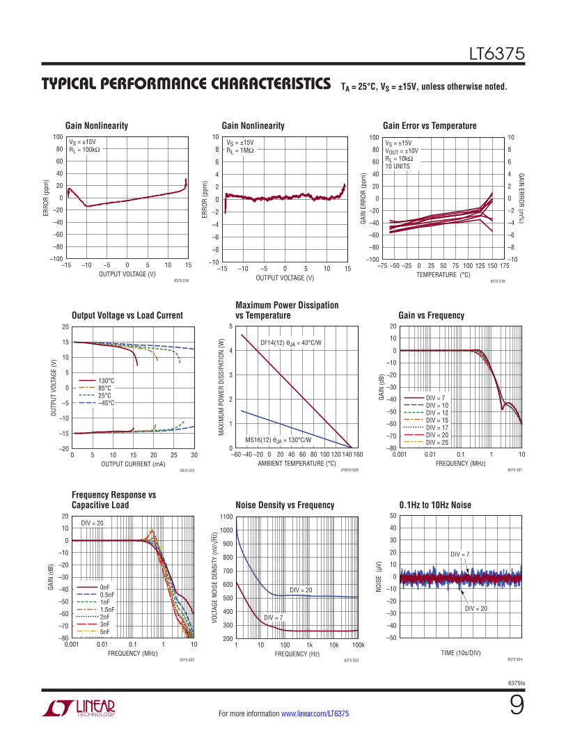
TYPICAL PERFORMANCE CHARACTERISTICS
Typical Distribution of Gain Error Typical Distribution of Gain Error Typical Distribution of Gain Error
Typical Distribution of CMRR Typical Distribution of CMRR Typical Distribution of CMRR
CMRR (µV/V = ppm)–40 –30 –20 –10 0 10 20 30 40
0
20
40
60
80
100
120
140
160
180
200
NUM
BER
OF U
NITS
6375 G01
1248 UNITSFROM 4 RUNSBOTH PACKAGES
VS = ±15VVIN = ±270VDIV = 25
655 UNITSFROM 2 RUNSMS16(12)
CMRR (µV/V = ppm)–40 –30 –20 –10 0 10 20 30 40
0
10
20
30
40
50
60
70
80
90
100
NUM
BER
OF U
NITS
6375 G02
VS = ±15VVIN = ±270VDIV = 25
593 UNITSFROM 2 RUNSDF14(12)
CMRR (µV/V = ppm)–40 –30 –20 –10 0 10 20 30 40
0
10
20
30
40
50
60
70
80
90
100
NUM
BER
OF U
NITS
6375 G03
VS = ±15VVIN = ±270VDIV = 25
GAIN ERROR (ppm)–50 –40 –30 –20 –10 0 10 20 30 40 50
0
50
100
150
200
250
300
350
400
NUM
BER
OF U
NITS
6375 G04
VS = ±15VVOUT = ±10V
1248 UNITSFROM 4 RUNSBOTH PACKAGES
655 UNITSFROM 2 RUNSMS16(12)
GAIN ERROR (ppm)–50 –40 –30 –20 –10 0 10 20 30 40 50
0
25
50
75
100
125
150
175
200
NUM
BER
OF U
NITS
6375 G05
VS = ±15VVOUT = ±10V
593 UNITSFROM 2 RUNSDF14(12)
VS = ±15VVOUT = ±10V
GAIN ERROR (ppm)–50 –40 –30 –20 –10 0 10 20 30 40 50
0
25
50
75
100
125
150
175
200
NUM
BER
OF U
NITS
6375 G06
TA = 25°C, VS = ±15V, unless otherwise noted.
ELECTRICAL CHARACTERISTICS
LT6375
86375fa
For more information www.linear.com/LT6375
TYPICAL PERFORMANCE CHARACTERISTICS
Typical Gain Error for Low Supply Voltages (Curves Offset for Clarity) Gain Nonlinearity Gain Nonlinearity
Typical Gain Error for RL = 10kΩ (Curves Offset for Clarity)
Typical Gain Error for RL = 5kΩ (Curves Offset for Clarity)
Typical Gain Error for RL = 2kΩ (Curves Offset for Clarity)
VS = ±18V
OUTPUT VOLTAGE (V)–20 –16 –12 –8 –4 0 4 8 12 16 20
OUTP
UT E
RROR
(2m
V/DI
V)
6375 G10
VS = ±15V
VS = ±12V
VS = ±10V
OUTPUT VOLTAGE (V)–20 –16 –12 –8 –4 0 4 8 12 16 20
OUTP
UT E
RROR
(2m
V/DI
V)
6375 G11
VS = ±18V
VS = ±15V
VS = ±12V
VS = ±10V
OUTPUT VOLTAGE (V)–20 –16 –12 –8 –4 0 4 8 12 16 20
OUTP
UT E
RROR
(2m
V/DI
V)
6375 G12
VS = ±18V
VS = ±15V
VS = ±12V
VS = ±10V
VS = ±5V, RL = 10kΩ
VS = ±5V, RL = 2kΩ
VS = ±5V, RL = 1kΩ
VS = ±2.5V, RL = 1kΩ
OUTPUT VOLTAGE (V)–5 –4 –3 –2 –1 0 1 2 3 4 5
OUTP
UT E
RROR
(2m
V/DI
V)
6375 G13
VS = ±15VRL = 2kΩ
OUTPUT VOLTAGE (V)–15 –10 –5 0 5 10 15
–100
–80
–60
–40
–20
0
20
40
60
80
100
ERRO
R (p
pm)
6375 G14
VS = ±15VRL = 10kΩ
OUTPUT VOLTAGE (V)–15 –10 –5 0 5 10 15
–100
–80
–60
–40
–20
0
20
40
60
80
100
ERRO
R (p
pm)
6375 G15
TA = 25°C, VS = ±15V, unless otherwise noted.
Typical Distribution of Gain Nonlinearity CMRR vs Frequency
Common Mode Voltage Range vs Power Supply Voltage
VS = ±15VVOUT = ±10V
GAIN NONLINEARITY (ppm)0 0.1 0.2 0.3 0.4 0.5 0.6 0.7 0.8 0.9 1
0
50
100
150
200
250
300
NUM
BER
OF U
NITS
6375 G07
1332 UNITSFROM 4 RUNSBOTH PACKAGES
FREQUENCY (Hz)10 100 1k 10k 100k 1M 10M
0
20
40
60
80
100
120
COM
MON
MOD
E RE
JECT
ION
RATI
O (d
B)
6375 G08
DIV = 7MS16(12)
DIV = 7DIV = 10DIV = 12DIV = 15DIV = 17DIV = 20DIV = 25OTT
POWER SUPPLY VOLTAGE (±V)0 5 10 15 20 25 30
–300
–250
–200
–150
–100
–50
0
50
100
150
200
250
300
COM
MON
MOD
E OP
ERAT
ING
RANG
E (V
)
LT6375 G09
LT6375
96375fa
For more information www.linear.com/LT6375
TYPICAL PERFORMANCE CHARACTERISTICS
Gain Nonlinearity Gain Nonlinearity Gain Error vs Temperature
Frequency Response vs Capacitive Load Noise Density vs Frequency 0.1Hz to 10Hz Noise
Output Voltage vs Load CurrentMaximum Power Dissipation vs Temperature Gain vs Frequency
VS = ±15VRL = 100kΩ
OUTPUT VOLTAGE (V)–15 –10 –5 0 5 10 15
–100
–80
–60
–40
–20
0
20
40
60
80
100
ERRO
R (p
pm)
6375 G16
VS = ±15VRL = 1MΩ
OUTPUT VOLTAGE (V)–15 –10 –5 0 5 10 15
–10
–8
–6
–4
–2
0
2
4
6
8
10
ERRO
R (p
pm)
6375 G17
VS = ±15VVOUT = ±10VRL = 10kΩ10 UNITS
TEMPERATURE (°C)–75 –50 –25 0 25 50 75 100 125 150 175
–100
–80
–60
–40
–20
0
20
40
60
80
100
–10
–8
–6
–4
–2
0
2
4
6
8
10
GAIN
ERR
OR (p
pm) GAIN ERROR (m
%)
6375 G18
130°C85°C25°C–45°C
OUTPUT CURRENT (mA)0 5 10 15 20 25 30
–20
–15
–10
–5
0
5
10
15
20
OUTP
UT V
OLTA
GE (V
)
6375 G19
DF14(12) θJA = 43°C/W
MS16(12) θJA = 130°C/W
AMBIENT TEMPERATURE (°C)–60 –40 –20 0 20 40 60 80 100 120 140 160
0
1
2
3
4
5
MAX
IMUM
POW
ER D
ISSI
PATI
ON (W
)
LT6375 G20
DIV = 7DIV = 10DIV = 12DIV = 15DIV = 17DIV = 20DIV = 25
FREQUENCY (MHz)0.001 0.01 0.1 1 10
–80
–70
–60
–50
–40
–30
–20
–10
0
10
20
GAIN
(dB)
6375 G21
DIV = 20
0nF0.5nF1nF1.5nF2nF3nF5nF
FREQUENCY (MHz)0.001 0.01 0.1 1 10
–80
–70
–60
–50
–40
–30
–20
–10
0
10
20
GAIN
(dB)
6375 G22
DIV = 7
DIV = 20
FREQUENCY (Hz)1 10 100 1k 10k 100k
200
300
400
500
600
700
800
900
1000
1100
VOLT
AGE
NOIS
E DE
NSIT
Y (n
V/√H
z)
6375 G23
DIV = 7
TIME (10s/DIV)
–50
–40
–30
–20
–10
0
10
20
30
40
50
NOIS
E (µ
V)
6375 G24
DIV = 20
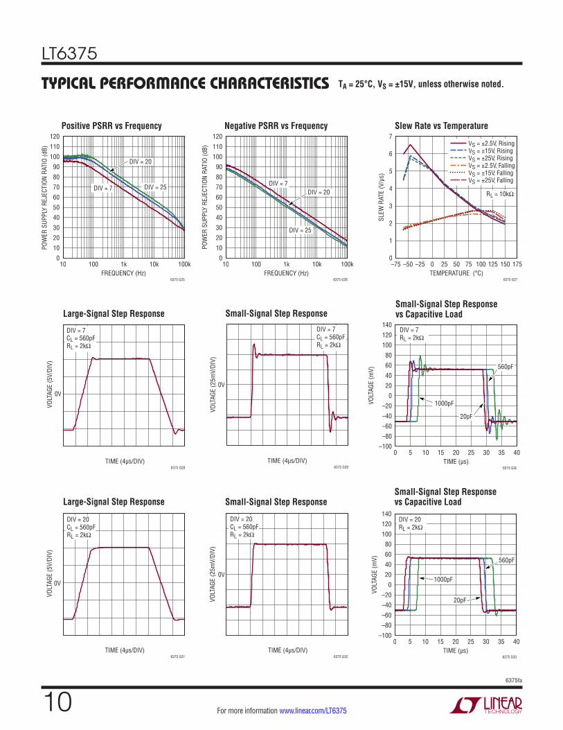
TA = 25°C, VS = ±15V, unless otherwise noted.
LT6375
106375fa
For more information www.linear.com/LT6375
TYPICAL PERFORMANCE CHARACTERISTICS
Small-Signal Step ResponseSmall-Signal Step Response vs Capacitive Load
Small-Signal Step ResponseSmall-Signal Step Response vs Capacitive Load
Large-Signal Step Response
Large-Signal Step Response
TIME (4µs/DIV)
VOLT
AGE
(5V/
DIV)
6375 G28
DIV = 7CL = 560pFRL = 2kΩ
0V
TIME (4µs/DIV)
VOLT
AGE
(25m
V/DI
V)
6375 G29
DIV = 7CL = 560pFRL = 2kΩ
0V
DIV = 7RL = 2kΩ
560pF
TIME (µs)0 5 10 15 20 25 30 35 40
–100
–80
–60
–40
–20
0
20
40
60
80
100
120
140
VOLT
AGE
(mV)
6375 G30
1000pF
20pF
DIV = 20CL = 560pFRL = 2kΩ
TIME (4µs/DIV)
VOLT
AGE
(5V/
DIV)
6375 G31
0V
TIME (4µs/DIV)
VOLT
AGE
(25m
V/DI
V)
6375 G32
DIV = 20CL = 560pFRL = 2kΩ
0V
560pF
TIME (µs)0 5 10 15 20 25 30 35 40
–100
–80
–60
–40
–20
0
20
40
60
80
100
120
140
VOLT
AGE
(mV)
6375 G33
DIV = 20RL = 2kΩ
1000pF
20pF
TA = 25°C, VS = ±15V, unless otherwise noted.
Positive PSRR vs Frequency Negative PSRR vs Frequency Slew Rate vs Temperature
DIV = 25
FREQUENCY (Hz)10 100 1k 10k 100k
0
10
20
30
40
50
60
70
80
90
100
110
120
POW
ER S
UPPL
Y RE
JECT
ION
RATI
O (d
B)
6375 G25
DIV = 7
DIV = 20
FREQUENCY (Hz)10 100 1k 10k 100k
0
10
20
30
40
50
60
70
80
90
100
110
120
POW
ER S
UPPL
Y RE
JECT
ION
RATI
O (d
B)
6375 G26
DIV = 25
DIV = 7DIV = 20 RL = 10kΩ
VS = ±2.5V, RisingVS = ±15V, RisingVS = ±25V, RisingVS = ±2.5V, FallingVS = ±15V, FallingVS = ±25V, Falling
TEMPERATURE (°C)–75 –50 –25 0 25 50 75 100 125 150 175
0
1
2
3
4
5
6
7
SLEW
RAT
E (V
/µs)
6375 G27

LT6375
116375fa
For more information www.linear.com/LT6375
TYPICAL PERFORMANCE CHARACTERISTICS
Settling Time Settling TimeOutput Offset Voltage vs Temperature
Thermal Shutdown Hysteresis
Quiescent Current vs SHDN Voltage
Quiescent Current vs Supply Voltage
Minimum Supply Voltage
Quiescent Current vs Temperature
Shutdown Quiescent Current vs Supply Voltage
10 UNITS
TEMPERATURE (°C)–75 –50 –25 0 25 50 75 100 125 150 175
200
250
300
350
400
450
500
550
QUIE
SCEN
T CU
RREN
T (µ
A)
6375 G37
TEMPERATURE (°C)145 150 155 160 165 170
0
100
200
300
400
500
600
SUPP
LY C
URRE
NT (µ
A)
6375 G38
VSHDN = 0V150°C125°C85°C
25°C–40°C–55°C
SUPPLY VOLTAGE (V)0 10 20 30 40 50
0
10
20
30
40
50
QUIE
SCEN
T CU
RREN
T (µ
A)
LT6375 G40
VS = ±15V
SHDN VOLTAGE (V)0 5 10 15
0
50
100
150
200
250
300
350
400
450
500
550
QUIE
SCEN
T CU
RREN
T (µ
A)
6375 G41
150°C125°C85°C
25°C–40°C–55°C
TA = 125°C
TA = 25°C
TA = –45°C
DIV = 7
TOTAL SUPPLY VOLTAGE (V)0 1 2 3 4 5
–150
–100
–50
0
50
100
150
CHAN
GE IN
OFF
SET
VOLT
AGE
(µV)
6375 G42
DIV = 7
ERROR VOLTAGE
TIME (10µs/DIV)
–1.0
–0.5
0
0.5
1.0
1.5
2.0
2.5
3.0
3.5
4.0
–4
–2
0
2
4
6
8
10
12
14
16
ERRO
R VO
LTAG
E (m
V)
OUTPUT VOLTAGE (V)
6375 G34
OUTPUT VOLTAGE
DIV = 7
ERROR VOLTAGE
TIME (10µs/DIV)
–4.0
–3.5
–3.0
–2.5
–2.0
–1.5
–1.0
–0.5
0
0.5
1.0
–16
–14
–12
–10
–8
–6
–4
–2
0
2
4
ERRO
R VO
LTAG
E (m
V)OUTPUT VOLTAGE (V)
6375 G35
OUTPUT VOLTAGE
TEMPERATURE (°C)–60 –40 –20 0 20 40 60 80 100 120 140
–3000
–2250
–1500
–750
0
750
1500
2250
3000
OFFS
ET V
OLTA
GE (µ
V)
6375 G36
DIV = 2010 UNITS
TA = 25°C, VS = ±15V, unless otherwise noted.
TA = 150°C
TA = –55°C
PARAMETRIC SWEEP IN ~25°C INCREMENTS
SUPPLY VOLTAGE (V)0 10 20 30 40 50
0
100
200
300
400
500
600
QUIE
SCEN
T CU
RREN
T (µ
A)
6375 G39
LT6375
126375fa
For more information www.linear.com/LT6375
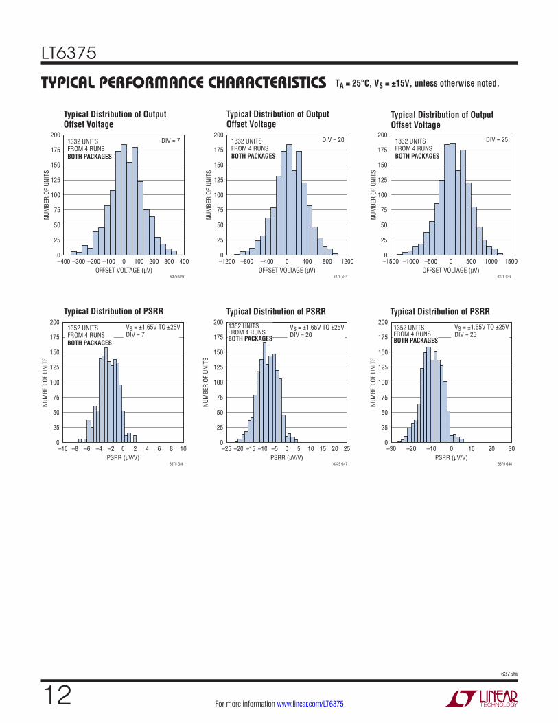
Typical Distribution of PSRR
TYPICAL PERFORMANCE CHARACTERISTICS
Typical Distribution of PSRR Typical Distribution of PSRR
VS = ±1.65V TO ±25VDIV = 7
PSRR (µV/V)–10 –8 –6 –4 –2 0 2 4 6 8 10
0
25
50
75
100
125
150
175
200
NUM
BER
OF U
NITS
6375 G46
1352 UNITSFROM 4 RUNSBOTH PACKAGES
VS = ±1.65V TO ±25VDIV = 20
PSRR (µV/V)–25 –20 –15 –10 –5 0 5 10 15 20 25
0
25
50
75
100
125
150
175
200
NUM
BER
OF U
NITS
6375 G47
1352 UNITSFROM 4 RUNSBOTH PACKAGES
VS = ±1.65V TO ±25VDIV = 25
PSRR (µV/V)–30 –20 –10 0 10 20 30
0
25
50
75
100
125
150
175
200
NUM
BER
OF U
NITS
6375 G48
1352 UNITSFROM 4 RUNSBOTH PACKAGES
TA = 25°C, VS = ±15V, unless otherwise noted.
Typical Distribution of Output Offset Voltage
Typical Distribution of Output Offset Voltage
Typical Distribution of Output Offset Voltage
DIV = 7
OFFSET VOLTAGE (µV)–400 –300 –200 –100 0 100 200 300 4000
25
50
75
100
125
150
175
200
NUM
BER
OF U
NITS
6375 G43
1332 UNITSFROM 4 RUNSBOTH PACKAGES
DIV = 20
OFFSET VOLTAGE (µV)–1200 –800 –400 0 400 800 12000
25
50
75
100
125
150
175
200
NUM
BER
OF U
NITS
6375 G44
1332 UNITSFROM 4 RUNSBOTH PACKAGES
DIV = 25
OFFSET VOLTAGE (µV)–1500 –1000 –500 0 500 1000 15000
25
50
75
100
125
150
175
200
NUM
BER
OF U
NITS
6375 G45
1332 UNITSFROM 4 RUNSBOTH PACKAGES
LT6375
136375fa
For more information www.linear.com/LT6375
PIN FUNCTIONSV+ (Pin 9/Pin 10): Positive Supply Pin.
V– (Exposed Pad Pin 15/Pin 8): Negative Supply Pin.
OUT (Pin 8/Pin 9): Output Pin.
+IN (Pin 1/Pin 1): Noninverting Input Pin. Accepts input voltages from 270V to –270V.
+REFA (Pin 3/Pin 3): Reference Pin A. Sets the input common mode range and the output noise and offset.
+REFB (Pin 4/Pin 5): Reference Pin B. Sets the input common mode range and the output noise and offset.
+REFC (Pin 5/Pin 6): Reference Pin C. Sets the input common mode range and the output noise and offset.
–IN (Pin 14/Pin 16): Inverting Input Pin. Accepts input voltages from 270V to –270V.
(DFN/MSOP)
–REFA (Pin 12/Pin 14): Reference Pin A. Sets the input common mode range and the output noise and offset.
–REFB (Pin 11/Pin 12): Reference Pin B. Sets the input common mode range and the output noise and offset.
–REFC (Pin 10/Pin 11): Reference Pin C. Sets the input common mode range and the output noise and offset.
REF (Pin 6/Pin 7): Reference Input. Sets the output level when the difference between the inputs is zero.
SHDN (Pin 7) DFN Only: Shutdown Pin. Amplifier is ac-tive when this pin is tied to V+ or left floating. Pulling the pin >2.5V below V+ causes the amplifier to enter a low power state.
LT6375
146375fa
For more information www.linear.com/LT6375
BLOCK DIAGRAM
–
+
V+
V–
V+
OUT
REF
–REFA
–IN
+IN
–REFB
19k 38k
190k
190k
190k
23.75k
–REFC
+REFA +REFB +REFC6375 BD
19k 38k
SHDN
10µA23.75k
190k
APPLICATIONS INFORMATIONTRANSFER FUNCTION
The LT6375 is a unity-gain difference amplifier with the transfer function:
VOUT = (V+IN – V–IN) + VREF
The voltage on the REF pin sets the output voltage when the differential input voltage (VDIFF = V+IN – V–IN) is zero. This reference is used to shift the output voltage to the desired input level of the next stage of the signal chain.
BENEFITS OF SELECTABLE RESISTOR DIVIDER RATIOS
The LT6375 offers smaller package size, better gain ac-curacy and better noise performance than existing high common mode voltage range difference amplifiers. Ad-ditionally, the LT6375 allows the user to maximize system performance by selecting the resistor divider ratio (DIV) appropriate to their input common mode voltage range. A higher resistor divider ratio (DIV) enables higher common mode voltage range at the input pins, but also increases output noise, output offset/drift and decreases the –3dB bandwidth. Therefore, a trade-off exists between input range and DC, AC, and drift performance of the part. It
is recommended that the user choose the lowest resistor divider ratio that achieves the required input common mode voltage range in their application to maximize the system SNR, precision and speed.
Table 1 shows the noise, offset/drift, and –3dB bandwidth of the LT6375 for all different reference pins configurations.
COMMON MODE VOLTAGE RANGE
The wide common mode voltage range of the LT6375 is enabled by both a resistor divider at the input of the op amp and by an internal op amp that can withstand high input voltages.
The internal resistor network of the LT6375 divides down the input common mode voltage. The resulting voltage at the op amp inputs determines the op amp’s operating region. In the configuration shown in Figure 1, a resistor divider is created at both op amp inputs by the 190k input resistor and the resistance from each input to ground, which is ~31.66k. The resistance to ground is formed by the 38k (REFB resistors) in parallel with the 190k (feed-back/REF resistor). The result is a divide by 7 of the input voltage. As shown in Tables 1 to 5, different connections to reference pins (i.e. pins +REFA, –REFA, +REFB, –REFB,

LT6375
156375fa
For more information www.linear.com/LT6375
–
+
V+
V–
VS+
VS+
V–IN
V+IN
VS–
OUT VOUT
REF
–REFA
–IN
+IN
–REFB
19k 38k
190k
190k
190k
23.75k
–REFC
+REFA +REFB +REFC6375 F01
19k 38k
SHDN
23.75k
190k
Figure 1. Basic Connections for Dual-Supply Operation (Resistor Divider Ratio = 7)
+REFC, –REFC) result in different resistor divider ratios (DIV) and different attenuation of the LT6375’s input common mode voltage.
The internal op amp of LT6375 has two operating regions: a) If the common mode voltage at the inputs of the internal op amp (VCMOP) is between V– and V+ –1.75V, the op amp operates in its normal region; b) If VCMOP is between V+ –1.75V and V– +76V, the op amp continues to operate, but in its Over-The-Top region with degraded performance (see Over-The-Top operation section of this data sheet for more detail).
Table 2 lists the valid input common mode voltage range for an LT6375 with different configurations of the refer-ence pins when used with dual power supplies. Using the voltage ranges in this table ensures that the internal op amp is operating in its normal (and best) region. The figure entitled Common Mode Voltage Range vs Power Supply Voltage, in the Typical Performance Characteristics section of this data sheet, illustrates the information in Table 2 graphically.
Table 3 lists the valid input common mode voltage range for an LT6375 that results in the internal op amp operating in its Over-The-Top region.
The reference pins can be connected to ground (as in Tables 2 and 3) or to any reference voltage. In order to achieve the specified gain accuracy and CMRR perfor-mance of the LT6375, this reference must have a very low impedance. The valid input common mode range changes depending on the voltages chosen for reference pins. One positive and one negative reference should always be con-nected to a low impedance voltage to ensure the stability of the amplifier. Table 4 lists the valid input common mode voltage range for an LT6375 when the part is used with a single power supply, and REF and the other reference pins are connected to mid-supply. If, as shown in Table 5, the REF pin remains connected to mid-supply, while the other reference pins are connected to ground, the result is a higher positive input range at the expense of a more restricted negative input range.
Table 1. LT6375 Performance at Different Resistor Divider RatiosRESISTOR DIVIDER OPTIONS RESISTOR
DIVIDER RATIO (DIV)
DIFFERENTIAL GAIN
OUTPUT NOISE AT
1kHz (nV/√Hz)MAXIMUM OFFSET
(µV)MAXIMUM OFFSET
DRIFT (µV/°C)
–3dB BANDWIDTH
(kHz)+REFA AND
–REFA+REFB AND
–REFB+REFC AND
–REFC REF
19k 38k 23.75k 190k LT6375A LT6375 LT6375A LT6375
OPEN GND OPEN REF 7 1 250 300 450 9 12 575
OPEN OPEN GND REF 10 1 307 380 600 12 16 530
GND OPEN OPEN REF 12 1 346 450 720 14 19 485
OPEN GND GND REF 15 1 410 540 900 16 22 445
GND GND OPEN REF 17 1 445 600 1000 19 25 405
GND OPEN GND REF 20 1 508 700 1200 23 30 375
GND GND GND REF 25 1 599 900 1500 28 37 310
APPLICATIONS INFORMATION
LT6375
166375fa
For more information www.linear.com/LT6375
APPLICATIONS INFORMATIONTable 2. Common Mode Voltage Operating Range with Dual Power Supplies (Normal Region)INPUT RANGE (REF = GND)
+REFA AND
–REFA
+REFB AND
–REFB
+REFC AND
–REFC DIV
VS = ±2.5V VS = ±15V VS = ±25V
HIGH LOW HIGH LOW HIGH LOW
OPEN GND OPEN 7 5.25 –17.5 92.75 –105 162.75 –175
OPEN OPEN GND 10 7.5 –25 132.5 –150 232.5 –250
GND OPEN OPEN 12 9 –30 159 –180 270 –270
OPEN GND GND 15 11.25 –37.5 198.75 –225 270 –270
GND GND OPEN 17 12.75 –42.5 225.25 –255 270 –270
GND OPEN GND 20 15 –50 265 –270 270 –270
GND GND GND 25 18.75 –62.5 270 –270 270 –270
Table 3. Common Mode Voltage Operating Range with Dual Power Supplies (Over-The-Top Region)INPUT RANGE (REF = GND)
+REFA AND
–REFA
+REFB AND
–REFB
+REFC AND
–REFC DIV
VS = ±2.5V VS = ±15V VS = ±25V
HIGH LOW HIGH LOW HIGH LOW
OPEN GND OPEN 7 270 –17.5 270 –105 270 –175
OPEN OPEN GND 10 270 –25 270 –150 270 –250
GND OPEN OPEN 12 270 –30 270 –180 270 –270
OPEN GND GND 15 270 –37.5 270 –225 270 –270
GND GND OPEN 17 270 –42.5 270 –255 270 –270
GND OPEN GND 20 270 –50 270 –270 270 –270
GND GND GND 25 270 –62.5 270 –270 270 –270
Table 4. Common Mode Voltage Operating Range with a Single Power Supply, References to Mid-Supply (Normal Region)INPUT RANGE (REF = VS/2)
+REFA AND
–REFA
+REFB AND
–REFB
+REFC AND
–REFC DIV
VS = 5V VS = 30V VS = 50V
HIGH LOW HIGH LOW HIGH LOW
OPEN VS/2 OPEN 7 7.75 –15 107.75 –90 187.75 –150
OPEN OPEN VS/2 10 10 –22.5 147.5 –135 257.5 –225
VS/2 OPEN OPEN 12 11.5 –27.5 174 –165 270 –270
OPEN VS/2 VS/2 15 13.75 –35 213.75 –210 270 –270
VS/2 VS/2 OPEN 17 15.25 –40 240.25 –240 270 –270
VS/2 OPEN VS/2 20 17.5 –47.5 270 –270 270 –270
VS/2 VS/2 VS/2 25 21.25 –60 270 –270 270 –270
Table 5. Common Mode Voltage Operating Range with a Single Power Supply, References to GND (Normal Region)INPUT RANGE (REF = VS/2)
+REFA AND
–REFA
+REFB AND
–REFB
+REFC AND
–REFC DIV
VS = 5V VS = 30V VS = 50V
HIGH LOW HIGH LOW HIGH LOW
OPEN GND OPEN 7 20.25 –2.5 182.75 –15 270 –25
OPEN OPEN GND 10 30 –2.5 267.5 –15 270 –25
GND OPEN OPEN 12 36.5 –2.5 270 –15 270 –25
OPEN GND GND 15 46.25 –2.5 270 –15 270 –25
GND GND OPEN 17 52.75 –2.5 270 –15 270 –25
GND OPEN GND 20 62.5 –2.5 270 –15 270 –25
GND GND GND 25 78.75 –2.5 270 –15 270 –25
The LT6375 will not operate correctly if the common mode voltage at its input pins goes below the range specified in above tables, but the part will not be damaged as long as the lowest common mode voltage at the inputs of the internal op amp (VCMOP) remains between V– –25V and V–. Also, the voltage at LT6375 input pins should never be higher than 270V or lower than –270V under any circumstances.
SHUTDOWN
The LT6375 in the DFN14 package has a shutdown pin (SHDN). Under normal operation this pin should be tied to V+ or allowed to float. Tying this pin to 2.5V below V+ will cause the part to enter a low power state. The sup-ply current is reduced to less than 25µA and the op amp output becomes high impedance.
SUPPLY VOLTAGE
The positive supply pin of the LT6375 should be bypassed with a small capacitor (typically 0.1µF) as close to the supply pin as possible. When driving heavy loads an additional 4.7µF electrolytic capacitor should be added. When using split supplies, the same is true for the V– supply pin.

LT6375
176375fa
For more information www.linear.com/LT6375
APPLICATIONS INFORMATIONACCURATE CURRENT MEASUREMENTS
The LT6375 can be used in high side, low side and bi-directional wide common mode range current sensing. Figure 2 shows the LT6375 sensing current by measuring the voltage across RSENSE. The added sense resistors create a CMRR error and a gain error. For RSENSE greater than 2Ω the source resistance mismatch degrades the CMRR. Adding a resistor equal in value to RSENSE in series with the +IN terminal (RC) eliminates this mismatch.
Using an RSENSE greater than 10Ω will cause the gain error to exceed the 0.006% specification of LT6375. This is due to the loading effects of the LT6375.
VOUT = ILOAD • RSENSE • 190k/(190k + RSENSE)
Increasing RSENSE and RC slightly to RSENSE' removes the gain error.
RSENSE' = RSENSE • 190k/(190k – RSENSE).
NOISE AND FILTERING
The noise performance of the LT6375 can be optimized both by appropriate choice of its internal attenuation set-ting and by the addition of a filter to the amplifier output (Figure 3). For applications that do not require the full bandwidth of the LT6375, the addition of an output filter will lower system noise. Table 6 shows the output noise for different internal resistor divider ratios and output filter bandwidths.
–
+
V+
V–
VS+
VS+ = 15V
RSENSE
VS– = –15V
OUT VOUT ≅ RSENSE • ILOAD
VSOURCE+ = 270V
VSOURCE– = –270V
ILOAD
ILOAD
VOUT ≅ RSENSE • ILOAD
REFVREF
–REFA
–IN
+IN
–REFB
19k 38k
190k
190k
190k
23.75k
–REFC
+REFA +REFB +REFC
19k 38k
SHDN
23.75k
RC
190k
–
+
V+
V–
VS+
VS+ = 15V
VS– = –15V
OUT
REFVREF
–REFA
–IN
+IN
–REFB
19k 38k
190k
190k
190k
23.75k
–REFC
+REFA +REFB +REFC6375 F02
19k 38k
SHDN
23.75k
190k
RCRSENSE
LOAD
Figure 2. Wide Voltage Range Current Sensing
LT6375
186375fa
For more information www.linear.com/LT6375
Figure 3. Output Filtering with 2-Pole Butterworth Filter
–
+
V+
V–
VS+
VS+
V–IN
V+IN
VS–
OUT
REFVREF
–REFA
–IN
+IN
–REFB
19k 38k
190k
190k
190k
23.75k
–REFC
+REFA +REFB +REFC6375 F03
19k 38k
SHDN
23.75k
R1 R2
C2
C1
190k
–
+VOUTLT6015
APPLICATIONS INFORMATION
Table 6. Output Noise (VP-P) for 2-Pole Butterworth Filter for Different Internal Resistor Divider RatiosCorner Frequency
7 10 12 15 17 20 25
No Filter 1705µV 1831µV 1901µV 2008µV 2073µV 2177µV 2330µV
100kHz 537µV 662µV 740µV 853µV 925µV 1030µV 1197µV
10kHz 169µV 210µV 236µV 274µV 298µV 334µV 393µV
1kHz 54µV 67µV 75µV 87µV 95µV 107µV 126µV
100Hz 18µV 22µV 25µV 29µV 32µV 36µV 43µV
Table 7. Component Values for Different 2-Pole Butterworth Filter BandwidthsCorner Frequency R1 R2 C1 C2
100kHz 11kΩ 11.3kΩ 100pF 200pF
10kHz 11kΩ 11.3kΩ 1nF 2nF
1kHz 11kΩ 11.3kΩ 10nF 20nF
100Hz 11kΩ 11.3kΩ 0.1µF 0.2µF
Figure 4. Current Measurement Application
–
+
V+
V–
15V
RSENSE10Ω
–15V
OUT VOUT
VSOURCE+ = 195V
1A REF
–REFA
–IN
+IN
–REFB
19k 38k
190k
190k
190k
23.75k
–REFC
+REFA +REFB +REFC6375 F04
19k 38k
SHDN
23.75k
RC, 10Ω
190k
LOAD

LT6375
196375fa
For more information www.linear.com/LT6375
ERROR BUDGET ANALYSIS
Figure 4 shows the LT6375 in a current measurement application. The error budget for this application is shown in Table 8. The resistor divider ratio is set to 15 to divide the 195V input common mode voltage down to 13V at the op amp inputs. The 1A current and 10Ω sense resistor produce an output full-scale voltage of 10V. Table 8 shows the error sources in parts per million (ppm) of the full-scale voltage across the temperature range of 25°C to 85°C.
Different sources of error contribute to the maximum ac-curacy that can be achieved in an application. Gain error, offset voltage and common mode rejection error combine to set the initial error. Additionally, the gain error and offset voltage drift across the temperature range. The excellent gain accuracy, low offset voltage, high CMRR, low offset voltage drift and low gain error drift of the LT6375 all combine to enable extremely accurate measurements.
Over-The-Top OPERATION
When the input common mode voltage of the internal op amp (VCMOP) in the LT6375 is biased near or above the V+ supply, the op amp is operating in the Over-The-Top region. The op amp continues to operate with an input common mode voltage of up to 76V above V– (regardless of the positive power supply voltage V+), but its performance is
Table 8. Error Budget Analysis
ERROR SOURCE LT6375A LT6375 COMPETITOR 1 COMPETITOR 2
ERROR, ppm of FS
LT6375A LT6375 COMPETITOR 1 COMPETITOR 2
Accuracy, TA = 25°C
Initial Gain Error 0.0035% FS 0.006% FS 0.02% FS 0.03% FS 35 60 200 300
Offset Voltage 540µV 900µV 1100µV 500µV 54 90 110 50
Common Mode 195V/96dB = 3090µV
195V/89dB = 6920µV
195V/90dB = 6166µV
195V/86dB = 9770µV
309 692 617 977
Total Accuracy Error 398 842 927 1327
Temperature Drift
Gain 1ppm/°C ×60°C 1ppm/°C ×60°C 10ppm/°C ×60°C 10ppm/°C ×60°C 60 60 600 600
Offset Voltage 16µV/°C ×60°C 22µV/°C ×60°C 15µV/°C ×60°C 10µV/°C ×60°C 96 132 90 60
Total Drift Error 156 192 690 660
Total Error 554 1034 1617 1987
APPLICATIONS INFORMATIONdegraded. The op amp’s input bias currents change from under ±2nA to 14µA. The op amp’s input offset current rises to ±50nA which adds ±9.5mV to the output offset voltage.
In addition, when operating in the Over-The-Top region, the differential input impedance decreases from 1MΩ in normal operation to approximately 3.7kΩ in Over-The-Top operation. This resistance appears across the summing nodes of the internal op amp and boosts noise and offset while decreasing speed. Noise and offset will increase by between 66% and 83% depending on the resistor divider ratio setting. The bandwidth will be reduced by 40% to 45%. For more detail on Over-The-Top operation, consult the LT6015 data sheet.
OUTPUT
The output of the LT6375 can typically swing to within 5mV of either rail with no load and is capable of sourcing and sinking approximately 25mA. The LT6375 is internally compensated to drive at least 1nF of capacitance under any output loading conditions. For larger capacitive loads, a 0.22µF capacitor in series with a 150Ω resistor between the output and ground will compensate the amplifier to drive capacitive loads greater than 1nF. Additionally, the LT6375 has more gain and phase margin as the resistor divider ratio is increased.
LT6375
206375fa
For more information www.linear.com/LT6375
The power dissipated in the internal resistors (PRESD) depends on the input voltage, the resistor divider ratio (DIV), the output voltage and the voltage on REF and the other reference pins. The following equations and Figure 5 show different components of PRESD corresponding to different groups of LT6375’s internal resistors (assuming that LT6375 is used with a dual supply configuration with REF and all reference pins at ground).
PRESDA = (V+IN)2/(190k + 190k/(DIV – 1)) PRESDB = (V–IN – V+IN/DIV)2/(190k) PRESDC = (V+IN/DIV)2/(190k/(DIV – 2)) PRESDD = (V+IN/DIV – VOUT)2/(190k) PRESD = PRESDA + PRESDB + PRESDC + PRESDD
PRESD simplifies to:
PRESD = 2(V+IN2((DIV – 1)/DIV – VOUT/V+IN) + VOUT
2)/190k
In general, PRESD increases with higher input voltage, higher resistor divider ratio (DIV), and lower output, REF and reference pin voltages.
Example: An LT6375 in a DFN package mounted on a PC board has a thermal resistance of 43°C/W. Operating on ±25V supplies and driving a 2.5kΩ load to 12.5V with V+IN = 270V and DIV = 25, the total power dissipation is given by:
PD = (50 • 0.6mA) + 12.52/2.5k + 2702/197.92k + (257.5 – 270/25)2/190k + (270/25)2/8.26k + (270/25 – 12.5)2/190k = 0.795W
APPLICATIONS INFORMATION
Figure 5. Power Dissipation Example
–
+
V+
V–
V–IN = 270V – VOUT
V+IN = 270V
= 257.5V
VS+ = 25V
VS_ = –25V
OUT VOUT = 12.5V
REF
–REFA
–IN
+IN
–REFB
19k 38k
190k
PRESDDPRESDC
PRESDB
PRESDA
190k
190k
23.75k
–REFC
+REFA +REFB +REFC6375 F05
19k 38k
SHDN
23.75k
190k
DISTORTION
The LT6375 features excellent distortion performance when the internal op amp is operating within the supply rails. Operating the LT6375 with input common mode voltages that go from normal to Over-The-Top operation will significantly degrade the LT6375’s linearity as the op amp must transition between two different input stages.
POWER DISSIPATION CONSIDERATIONS
Because of the ability of the LT6375 to operate on power supplies up to ±25V, to withstand very high input volt-ages and to drive heavy loads, there is a need to ensure the die junction temperature does not exceed 150°C. The LT6375 is housed in DF14 (θJA = 43°C/W, θJC = 4°C/W) and MS16 (θJA = 130°C/W) packages.
In general, the die junction temperature (TJ) can be esti-mated from the ambient temperature (TA), and the device power dissipation (PD):
TJ = TA + PD • θJA
Power is dissipated by the amplifier’s quiescent current, by the output current driving a resistive load and by the input current driving the LT6375’s internal resistor network.
PD = ((VS+ – VS
–) • IS) + POD + PRESD
For a given supply voltage, the worst-case output power dissipation POD(MAX) occurs with the output voltage at half of either supply voltage. POD(MAX) is given by:
POD(MAX) = (VS/2)2/RLOAD
LT6375
216375fa
For more information www.linear.com/LT6375
APPLICATIONS INFORMATIONAssuming a thermal resistance of 43°C/W, the die tem-perature will experience a 34°C rise above ambient. This implies that the maximum ambient temperature the LT6375 should operate under the above conditions is:
TA =150°C – 34°C = 116°C
Keep in mind that the DFN package has an exposed pad which can be used to lower the θJA of the package. The more PCB metal connected to the exposed pad, the lower the thermal resistance.
The MSOP package has no exposed pad and a higher thermal resistance (θJA = 130°C/W). It should not be used in applications which have a high ambient temperature, require driving a heavy load, or require an extreme input voltage.
THERMAL SHUTDOWN
For safety, the LT6375 will enter shutdown mode when the die temperature rises to approximately 163°C. This thermal shutdown has approximately 9°C of hysteresis requiring the die temperature to cool 9°C before enabling the amplifier again.
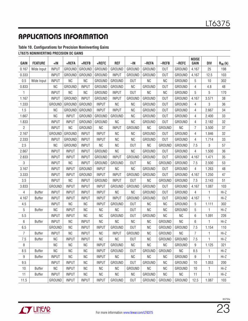
USE AT OTHER PRECISION DC GAINS
The array of resistors within the LT6375 provides numer-ous configurable connections that provide precision gains other than the unity differential gain options described previously. Note that only the +IN and –IN pins can oper-ate outside of the supply window. Since most of these alternate configurations involve driving the REFx pins, as well as the +IN and –IN pins, the input signals must be less than the supply voltages. Fully differential gains are available as shown in Table 9, and may be output-shifted with a REF offset signal. These configurations allow the LT6375 to be used as a versatile precision gain block with essentially no external components besides the supply decoupling. In most cases, only a single positive supply will be required. In Table 9, connections are identified as NC (no connect), INPUT (refers to both inputs driven, +signal to +pins,–signal to –pins), CROSS (refers to inputs cross-coupled, +signal to –pins, –signal to +pins), OUT (refers to the output fed back to –pins), or REF (refers to
connecting the REF pin to +pins). The same configurations provide inverting gains by grounding any pins intended for the +signal source. The differential input resistance is also tabulated as well as the amplification factor of the internal gain section involved (noise-gain, which helps to estimate the error-budget of the configuration).
Single-ended noninverting gains are also available as shown in Table 10, including many that operate as buffers (loaded only by the op amp input bias). A rich option set exists by using the REF pin as an additional variable. Two attenuation options exist that can accept signals outside the power supply range since they only drive the +IN pin. In Table 10, connections are identified as NC (no connect), INPUT (driven by the input), OUT (fed back from the output), or GROUND (grounded). Table 10 also includes tabulations of the internal resistor divider (DIV), noise gain (re-amplification), and the input loading presented by the circuit.
USE AS PRECISION AC GAIN BLOCK
In AC-coupled applications operating from a single power supply, it is useful to set the output voltage at mid-supply to maximize dynamic range. The LT6375 readily supports this with no additional biasing components by connecting specific pins to the V+ and V– potentials and AC-coupling the signal paths. Table 11 shows the available inverting gains and also tabulates the load resistances presented at the input. In Table 11, connections are identified as NC (no connect), AC IN (AC-coupled to the input) OUT (fed back from the output), tied to V+, tied to V–, or AC GND (AC- grounded). All pins that require an AC ground can share a single bypass capacitor. Likewise, all pins driven from the source signal may share a coupling capacitor as well. The output should also connect to the load circuitry using a coupling capacitor to block the mid-supply DC voltage.
The LT6375 may also be used for single-supply nonin-verting AC gains by employing a combination of input attenuation and re-amplification. With numerous choices of attenuation and re-amplification, several hundred overall gain combinations are possible, ranging from 0.167 to 23. The combinations are more plentiful than the DC configura-tions because there is no constraint on matching internal source resistances to minimize offset.
LT6375
226375fa
For more information www.linear.com/LT6375
Table 9. Configurations for Precision Differential Gains Other Than UnityLT6375 DIFFERENTIAL AND INVERTING PRECISION DC GAINS
GAIN ±IN ±REFA ±REFB ±REFC REF DIFF RIN (k) NOISE GAIN
0.167 CROSS INPUT OUT/REF CROSS REF 20 4.2
0.333 NC INPUT OUT/REF CROSS REF 21 4.0
0.5 INPUT INPUT OUT/REF CROSS REF 20 4.2
1.5 OUT/REF NC CROSS INPUT REF 29 7.5
2 CROSS NC CROSS INPUT REF 27 15.0
2.5 OUT/REF INPUT CROSS NC REF 25 8.5
2.833 CROSS INPUT OUT/REF INPUT REF 20 4.2
3 NC INPUT OUT/REF INPUT REF 21 4.0
3.167 INPUT INPUT OUT/REF INPUT REF 20 4.2
3.5 OUT/REF INPUT INPUT CROSS REF 17 12.5
4 CROSS NC INPUT NC REF 63 7.0
5 NC NC INPUT NC REF 76 6.0
6 INPUT NC INPUT NC REF 63 7.0
7 CROSS NC NC INPUT REF 42 10.0
8 NC NC NC INPUT REF 48 9.0
9 INPUT NC NC INPUT REF 42 10.0
10 NC INPUT NC NC REF 38 11.0
11 INPUT INPUT NC NC REF 35 12.0
12 CROSS NC INPUT INPUT REF 27 15.0
13 NC NC INPUT INPUT REF 29 14.0
14 INPUT NC INPUT INPUT REF 27 15.0
15 NC INPUT INPUT NC REF 25 16.0
16 INPUT INPUT INPUT NC REF 24 17.0
17 CROSS INPUT NC INPUT REF 20 20.0
18 NC INPUT NC INPUT REF 21 19.0
19 INPUT INPUT NC INPUT REF 20 20.0
22 CROSS INPUT INPUT INPUT REF 16 25.0
23 NC INPUT INPUT INPUT REF 17 24.0
24 INPUT INPUT INPUT INPUT REF 16 25.0
APPLICATIONS INFORMATIONThe input attenuator section dedicates some pins to es-tablishing a mid-supply bias point and with the remaining pins, provides several choices of input signal division fac-tors as shown in Table 12. The high attenuations that only use +IN for the signal path can accept waveform peaks that significantly exceed the supply range. Table 12 also includes tabulations of the resulting AC load resistance presented to the signal source. Here again, all pins that require an AC-ground connection may share a single by-pass capacitor, and all AC signal connections may share
a coupling capacitor. Note that configurations with +IN to V+ will bias at 50% of supply, while the others shown will bias at 38% of supply.
The single-supply AC-coupled noninverting circuit is completed by configuring the post-attenuator amplifica-tion factor. Table 13 shows the available re-amplification factors. Once again, all pins that require an AC-ground connection may share a single bypass capacitor, and the output should use a coupling capacitor to its load destination as well.
LT6375
236375fa
For more information www.linear.com/LT6375
Table 10. Configurations for Precision Noninverting GainsLT6375 NONINVERTING PRECISION DC GAINS
GAIN FEATURE +IN +REFA +REFB +REFC REF –IN –REFA –REFB –REFCNOISE GAIN DIV RIN (k)
0.167 Wide Input INPUT GROUND GROUND GROUND GROUND GROUND GROUND OUT GROUND 4.167 25 198
0.333 INPUT GROUND GROUND GROUND INPUT GROUND GROUND OUT GROUND 4.167 12.5 103
0.5 Wide Input INPUT NC NC GROUND GROUND OUT NC NC GROUND 5 10 302
0.833 NC GROUND INPUT GROUND GROUND NC GROUND OUT GROUND 4 4.8 48
1 INPUT NC NC GROUND INPUT OUT NC NC GROUND 5 5 170
1.167 INPUT GROUND INPUT GROUND INPUT GROUND GROUND OUT GROUND 4.167 3.571 38
1.333 GROUND GROUND GROUND INPUT NC NC GROUND OUT GROUND 4 3 36
1.5 NC GROUND GROUND INPUT INPUT NC GROUND OUT GROUND 4 2.667 34
1.667 NC INPUT GROUND GROUND GROUND NC GROUND OUT GROUND 4 2.400 33
1.833 INPUT INPUT GROUND GROUND NC NC GROUND OUT GROUND 4 2.182 32
2 INPUT NC GROUND NC INPUT GROUND NC GROUND NC 7 3.500 37
2.167 GROUND GROUND INPUT INPUT NC NC GROUND OUT GROUND 4 1.846 32
2.333 INPUT GROUND INPUT INPUT NC NC GROUND OUT GROUND 4 1.714 33
2.5 NC GROUND INPUT NC NC OUT NC GROUND GROUND 7.5 3 57
2.667 INPUT INPUT INPUT GROUND NC NC GROUND OUT GROUND 4 1.500 36
2.833 INPUT INPUT INPUT GROUND INPUT GROUND GROUND OUT GROUND 4.167 1.471 35
3 INPUT NC INPUT GROUND GROUND OUT NC GROUND GROUND 7.5 2.500 53
3.167 INPUT INPUT GROUND INPUT NC NC GROUND OUT GROUND 4 1.263 48
3.333 INPUT INPUT GROUND INPUT INPUT GROUND GROUND OUT GROUND 4.167 1.250 47
3.5 INPUT NC INPUT GROUND INPUT OUT NC GROUND GROUND 7.5 2.143 51
3.833 GROUND INPUT INPUT INPUT GROUND GROUND GROUND OUT GROUND 4.167 1.087 103
4 Buffer INPUT INPUT INPUT INPUT NC NC GROUND OUT GROUND 4 1 Hi-Z
4.167 Buffer INPUT INPUT INPUT INPUT INPUT GROUND GROUND OUT GROUND 4.167 1 Hi-Z
4.5 INPUT NC NC INPUT GROUND OUT NC NC GROUND 5 1.111 302
5 Buffer NC INPUT NC NC NC OUT NC NC GROUND 5 1 Hi-Z
5.5 INPUT INPUT NC NC GROUND OUT GROUND NC NC 6 1.091 226
6 Buffer INPUT NC INPUT NC NC NC NC GROUND NC 6 1 Hi-Z
6.5 GROUND NC INPUT INPUT GROUND OUT NC GROUND GROUND 7.5 1.154 110
7 Buffer INPUT NC INPUT NC INPUT GROUND NC GROUND NC 7 1 Hi-Z
7.5 Buffer NC INPUT INPUT NC NC OUT NC GROUND GROUND 7.5 1 Hi-Z
8 NC NC NC INPUT GROUND NC NC NC GROUND 9 1.125 321
8.5 Buffer NC NC NC INPUT GROUND OUT GROUND GROUND NC 8.5 1 Hi-Z
9 Buffer INPUT NC NC INPUT NC NC NC NC GROUND 9 1 Hi-Z
9.5 INPUT INPUT NC INPUT GROUND OUT GROUND NC GROUND 10 1.053 200
10 Buffer NC INPUT NC NC NC GROUND NC NC GROUND 10 1 Hi-Z
11 Buffer INPUT INPUT NC NC NC NC GROUND NC NC 11 1 Hi-Z
11.5 GROUND INPUT INPUT INPUT GROUND OUT GROUND GROUND GROUND 12.5 1.087 103
APPLICATIONS INFORMATION
LT6375
246375fa
For more information www.linear.com/LT6375
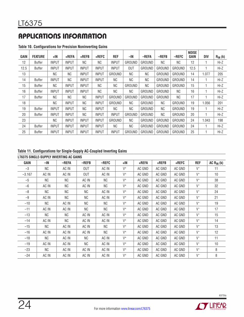
APPLICATIONS INFORMATIONTable 10. Configurations for Precision Noninverting Gains
GAIN FEATURE +IN +REFA +REFB +REFC REF –IN –REFA –REFB –REFCNOISE GAIN DIV RIN (k)
12 Buffer INPUT INPUT NC NC INPUT GROUND GROUND NC NC 12 1 Hi-Z
12.5 Buffer INPUT INPUT INPUT INPUT INPUT OUT GROUND GROUND GROUND 12.5 1 Hi-Z
13 NC NC INPUT INPUT GROUND NC NC GROUND GROUND 14 1.077 205
14 Buffer INPUT NC INPUT INPUT NC NC NC GROUND GROUND 14 1 Hi-Z
15 Buffer NC INPUT INPUT NC NC GROUND NC GROUND GROUND 15 1 Hi-Z
16 Buffer INPUT INPUT INPUT NC NC NC GROUND GROUND NC 16 1 Hi-Z
17 Buffer NC NC NC INPUT GROUND GROUND GROUND GROUND NC 17 1 Hi-Z
18 NC INPUT NC INPUT GROUND NC GROUND NC GROUND 19 1.056 201
19 Buffer INPUT INPUT NC INPUT NC NC GROUND NC GROUND 19 1 Hi-Z
20 Buffer INPUT INPUT NC INPUT INPUT GROUND GROUND NC GROUND 20 1 Hi-Z
23 NC INPUT INPUT INPUT GROUND NC GROUND GROUND GROUND 24 1.043 198
24 Buffer INPUT INPUT INPUT INPUT NC NC GROUND GROUND GROUND 24 1 Hi-Z
25 Buffer INPUT INPUT INPUT INPUT INPUT GROUND GROUND GROUND GROUND 25 1 Hi-Z
Table 11. Configurations for Single-Supply AC-Coupled Inverting GainsLT6375 SINGLE-SUPPLY INVERTING AC GAINS
GAIN –IN –REFA –REFB –REFC +IN +REFA +REFB +REFC REF AC RIN (k)
–3 NC AC IN OUT AC IN V+ AC GND AC GND AC GND V– 11
–3.167 AC IN AC IN OUT AC IN V+ AC GND AC GND AC GND V– 10
–5 NC NC AC IN NC V+ AC GND AC GND AC GND V– 38
–6 AC IN NC AC IN NC V+ AC GND AC GND AC GND V– 32
–8 NC NC NC AC IN V+ AC GND AC GND AC GND V– 24
–9 AC IN NC NC AC IN V+ AC GND AC GND AC GND V– 21
–10 NC AC IN NC NC V+ AC GND AC GND AC GND V– 19
–11 AC IN AC IN NC NC V+ AC GND AC GND AC GND V– 17
–13 NC NC AC IN AC IN V+ AC GND AC GND AC GND V– 15
–14 AC IN NC AC IN AC IN V+ AC GND AC GND AC GND V– 14
–15 NC AC IN AC IN NC V+ AC GND AC GND AC GND V– 13
–16 AC IN AC IN AC IN NC V+ AC GND AC GND AC GND V– 12
–18 NC AC IN NC AC IN V+ AC GND AC GND AC GND V– 11
–19 AC IN AC IN NC AC IN V+ AC GND AC GND AC GND V– 10
–23 NC AC IN AC IN AC IN V+ AC GND AC GND AC GND V– 8
–24 AC IN AC IN AC IN AC IN V+ AC GND AC GND AC GND V– 8

LT6375
256375fa
For more information www.linear.com/LT6375
APPLICATIONS INFORMATIONTable 12. Configurations for Single-Supply AC-Coupled Input AttenuationsLT6375 SINGLE-SUPPLY AC ATTENUATOR CONFIGURATIONS
DIV +IN +REFA +REFB +REFC REF AC RIN (k)
1.087 V+ AC IN AC IN AC IN V– 103
1.111 V+ AC IN NC AC IN V– 106
1.133 V+ AC IN AC IN NC V– 108
1.154 V+ NC AC IN AC IN V– 110
1.2 V+ AC IN NC NC V– 114
1.25 V+ NC NC AC IN V– 119
1.389 V+ AC IN AC GND AC IN V– 38
1.4 V+ NC AC IN NC V– 133
1.7 V+ AC IN AC GND NC V– 46
1.875 V+ NC AC GND AC IN V– 51
1.923 V+ AC GND AC IN AC IN V– 30
2.083 AC IN AC IN V+ V– AC IN 30
2.182 AC IN AC IN V+ V– NC 32
2.273 AC IN AC IN V+ V– AC GND 31
2.3 NC AC IN V+ V– NC 34
2.4 NC AC IN V+ V– AC GND 33
2.5 V+ AC IN AC GND AC GND V– 32
3.125 V+ AC GND AC GND AC IN V– 35
3.4 V+ AC GND AC IN NC V– 54
5 V+ AC GND AC IN AC GND V– 47
7.5 AC IN NC V+ V– AC IN 110
12 AC IN AC GND V+ V– AC IN 103
14 AC IN NC V+ V– NC 205
15 AC IN NC V+ V– AC GND 204
24 AC IN AC GND V+ V– NC 198
25 AC IN AC GND V+ V– AC GND 198

LT6375
266375fa
For more information www.linear.com/LT6375
APPLICATIONS INFORMATIONTable 13. Configurations for Single-Supply AC-Coupled Re-AmplicationsLT6375 NONINVERTING AC RE-AMPLIFICATIONS
GAIN –IN –REFA –REFB –REFC
4 NC AC GND OUT AC GND
4.167 AC GND AC GND OUT AC GND
5 OUT NC NC AC GND
6 NC NC AC GND NC
7 AC GND NC AC GND NC
7.5 OUT NC AC GND AC GND
8.5 OUT AC GND AC GND NC
9 NC NC NC AC GND
10 AC GND NC NC AC GND
11 NC AC GND NC NC
12 AC GND AC GND NC NC
12.5 OUT AC GND AC GND AC GND
14 NC NC AC GND AC GND
15 AC GND NC AC GND AC GND
16 NC AC GND AC GND NC
17 AC GND AC GND AC GND NC
19 NC AC GND NC AC GND
20 AC GND AC GND NC AC GND
24 NC AC GND AC GND AC GND
25 AC GND AC GND AC GND AC GND

LT6375
276375fa
For more information www.linear.com/LT6375
TYPICAL APPLICATIONS
–
+
V+
V–
VBAT = 48V
VS = 12V
VBAT
6OUT VOUT =
REF
–REFA
–IN
+IN
–REFB
19k 38k
190k
190k
190k
23.75k
–REFC
+REFA +REFB +REFC6375 TA02
19k 38k
SHDN
23.75k
190k
–
+
V+
V–
VS = 3.3V TO 50V
OUT VOUT
REF
–REFA
–IN2.2µF
2.2µF
+IN
–REFB
19k 38k
190kVIN
190k
190k
23.75k
–REFC
+REFA +REFB +REFC6375 TA03
19k 38k
SHDN
23.75k
190k
VOUT
VIN= –24
2.2µF
Telecom Supply Monitor
27dB Audio Gain Stage
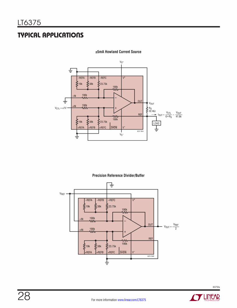
LT6375
286375fa
For more information www.linear.com/LT6375
TYPICAL APPLICATIONS
–
+
V+
V–
VS+
VS–
OUT
REF
–REFA
–IN
+IN
–REFB
19k 38k
190k
VCTL = ±1V
190k
190k
23.75k
–REFC
+REFA +REFB +REFC6375 TA04
19k 38k
SHDN
23.75k
190k
VCTL
RS32.4Ω
6 • RSIOUT =
VOUT
41.6k
LOAD
–
VOUT
–
+
V+
V–
OUT
REF
–REFA
–IN
+IN
–REFB
19k 38k
190k
VREF
190k
190k
23.75k
–REFC
+REFA +REFB +REFC6375 TA05
19k 38k
SHDN
23.75k
190k
VREF
2VOUT =
±5mA Howland Current Source
Precision Reference Divider/Buffer
LT6375
296375fa
For more information www.linear.com/LT6375
PACKAGE DESCRIPTIONPlease refer to http://www.linear.com/product/LT6375#packaging for the most recent package drawings.
4.00 ±0.10(4 SIDES)
NOTE:1. PACKAGE OUTLINE DOES NOT CONFORM TO JEDEC MO-2292. DRAWING NOT TO SCALE3. ALL DIMENSIONS ARE IN MILLIMETERS4. DIMENSIONS OF EXPOSED PAD ON BOTTOM OF PACKAGE DO NOT INCLUDE MOLD FLASH. MOLD FLASH, IF PRESENT, SHALL NOT EXCEED 0.15mm ON ANY SIDE5. EXPOSED PAD SHALL BE SOLDER PLATED6. SHADED AREA IS ONLY A REFERENCE FOR PIN 1 LOCATION ON THE TOP AND BOTTOM OF PACKAGE
PIN 1TOP MARK(NOTE 6)
0.40 ±0.10
17
148
BOTTOM VIEW—EXPOSED PAD
1.70 ±0.10
0.75 ±0.05
R = 0.115TYP
0.25 ±0.050.50 BSC
3.00 REF
3.38 ±0.10
0.200 REF
0.00 – 0.05
(DF14)(12) DFN 1113 REV 0
RECOMMENDED SOLDER PAD PITCH AND DIMENSIONSAPPLY SOLDER MASK TO AREAS THAT ARE NOT SOLDERED
0.70 ±0.05
0.25 ±0.050.50 BSC
3.10 ±0.05
4.50 ±0.05
PACKAGE OUTLINE
PIN 1 NOTCH0.35 × 45°CHAMFER
1.70 ±0.05
3.38 ±0.05
3.00 REF1.00BSC
1.00BSC
DF Package14(12)-Lead Plastic DFN (4mm × 4mm)(Reference LTC DWG # 05-08-1963 Rev Ø)
LT6375
306375fa
For more information www.linear.com/LT6375
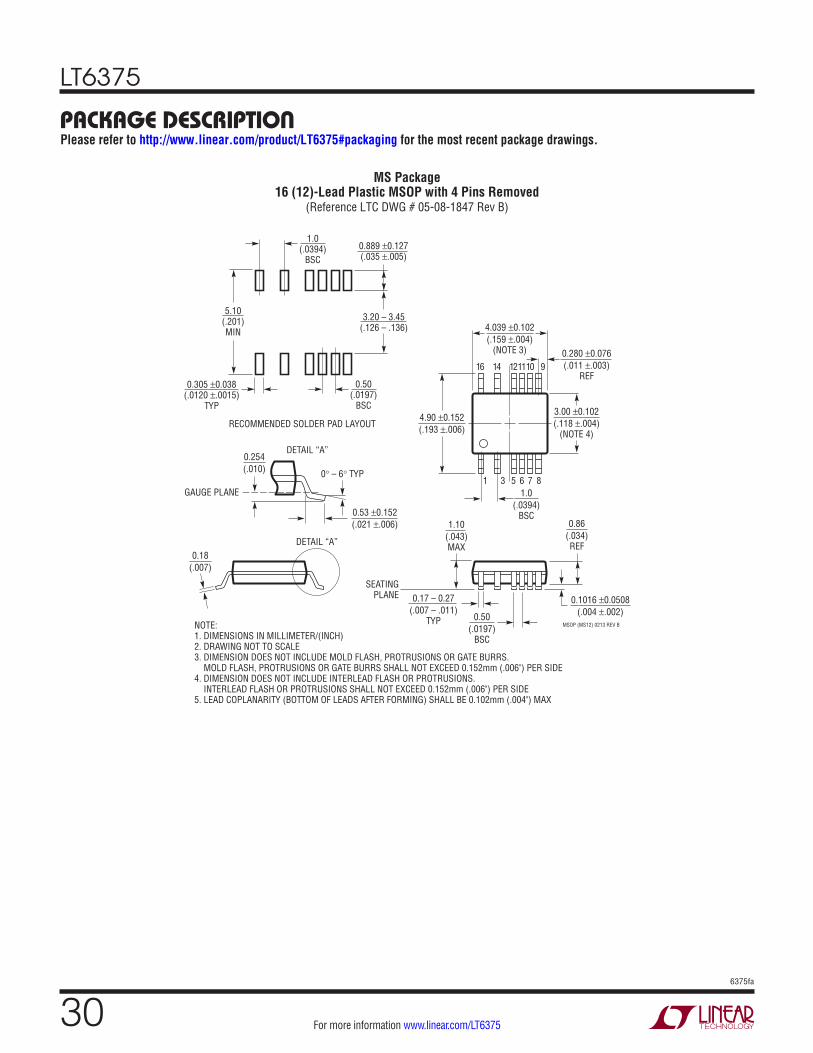
PACKAGE DESCRIPTIONPlease refer to http://www.linear.com/product/LT6375#packaging for the most recent package drawings.
MSOP (MS12) 0213 REV B
0.53 ±0.152(.021 ±.006)
SEATINGPLANE
0.18(.007)
1.10(.043)MAX
0.17 – 0.27(.007 – .011)
TYP
0.86(.034)REF
1.0(.0394)
BSC
0.50(.0197)
BSC
16 14 121110
1 3 5 6 7 8
9
NOTE:1. DIMENSIONS IN MILLIMETER/(INCH)2. DRAWING NOT TO SCALE3. DIMENSION DOES NOT INCLUDE MOLD FLASH, PROTRUSIONS OR GATE BURRS. MOLD FLASH, PROTRUSIONS OR GATE BURRS SHALL NOT EXCEED 0.152mm (.006") PER SIDE4. DIMENSION DOES NOT INCLUDE INTERLEAD FLASH OR PROTRUSIONS. INTERLEAD FLASH OR PROTRUSIONS SHALL NOT EXCEED 0.152mm (.006") PER SIDE5. LEAD COPLANARITY (BOTTOM OF LEADS AFTER FORMING) SHALL BE 0.102mm (.004") MAX
0.254(.010) 0° – 6° TYP
DETAIL “A”
DETAIL “A”
GAUGE PLANE
5.10(.201)MIN
3.20 – 3.45(.126 – .136)
0.889 ±0.127(.035 ±.005)
RECOMMENDED SOLDER PAD LAYOUT
0.305 ±0.038(.0120 ±.0015)
TYP
0.50(.0197)
BSC
1.0(.0394)
BSC
4.039 ±0.102(.159 ±.004)
(NOTE 3)
0.1016 ±0.0508(.004 ±.002)
3.00 ±0.102(.118 ±.004)
(NOTE 4)
0.280 ±0.076(.011 ±.003)
REF
4.90 ±0.152(.193 ±.006)
MS Package16 (12)-Lead Plastic MSOP with 4 Pins Removed
(Reference LTC DWG # 05-08-1847 Rev B)

LT6375
316375fa
For more information www.linear.com/LT6375
Information furnished by Linear Technology Corporation is believed to be accurate and reliable. However, no responsibility is assumed for its use. Linear Technology Corporation makes no representa-tion that the interconnection of its circuits as described herein will not infringe on existing patent rights.
REVISION HISTORYREV DATE DESCRIPTION PAGE NUMBER
A 12/15 Added A-grade. 1-7, 15, 19

LT6375
326375fa
For more information www.linear.com/LT6375 LINEAR TECHNOLOGY CORPORATION 2015
LT 1215 REV A • PRINTED IN USALinear Technology Corporation1630 McCarthy Blvd., Milpitas, CA 95035-7417(408) 432-1900 FAX: (408) 434-0507 www.linear.com/LT6375
RELATED PARTS
TYPICAL APPLICATION
PART NUMBER DESCRIPTION COMMENTS
LT1990 ±250V Input Range Difference Amplifier 2.7V to 36V Operation, CMRR > 70dB, Input Voltage = ±250V
LT1991 Precision, 100µA Gain Selectable Amplifier 2.7V to 36V Operation, 50μV Offset, CMRR > 75B, Input Voltage = ±60V
LT1996 Precision, 100µA Gain Selectable Amplifier Micropower, Pin Selectable Up to Gain = 118
LT1999 High Voltage, Bidirectional Current Sense Amplifier
–5V to 80V, 750 µV, CMRR 80dB 100kHz Gain: 10V/V, 20V/V, 50V/V
LT6015/LT6016/LT6017
Single, Dual, and Quad, Over-The-Top Precision Op Amp
3.2MHz, 0.8V/µs, 50µV VOS, 3V to 50V VS, 0.335mA IS, RRIO
LTC6090 140V Operational Amplifier 50pA IB, 1.6mV VOS, 9.5V to 140V VS, 4.5mA IS, RR Output
LT6108 High Side Current Sense Amplifier with Reference and Comparator with Shutdown
2.7V to 60V, 125µV, Resistor Set Gain, ±1.25% Threshold Error
LT1787/ LT1787HV
Precision, Bidirectional High Side Current Sense Amplifier
2.7V to 60V Operation, 75μV Offset, 60μA Current Draw
LTC6101/ LTC6101HV
High Voltage High Side Current Sense Amplifier
4V to 60V/5V to 100V Operation, External Resistor Set Gain, SOT23
LTC6102/ LTC6102HV
Zero Drift High Side Current Sense Amplifier 4V to 60V/5V to 100V Operation, ±10μV Offset, 1μs Step Response, MSOP8/DFN Packages
LTC6104 Bidirectional, High Side Current Sense 4V to 60V, Gain Configurable, 8-Pin MSOP Package
Bidirectional Full Range Current Monitor
–
+
V+
V–
VMON = 0V TO 3V
OUTVOUT = VREF + 24 • (VSENSE)
VS = 5V (OR 2V GREATER THAN VMON)
VREF = 1.25VREF
–REFA
–IN
+IN
–REFB
19k 38k
190k
190k
190k
23.75k
–REFC
+REFA +REFB +REFC6375 TA06
19k 38k
SHDN
23.75k
RSENSE
190k
LOAD
NOTE: OPERATES OVER FULL RANGE OF LOAD VOLTAGE