m028633 mf0icu1 functional spec v3.3 - proxmark mhz - mifare... · 2010. 7. 7. · is the sak...
TRANSCRIPT

1. General description
NXP has developed the MIFARE MF0ICU1 to be used with Proximity Coupling Devices (PCD) according to ISO/IEC14443 Type A, it can act as single trip tickets in public transportation networks, loyalty cards or day passes for events. They are the ideal replacement for conventional ticketing solutions such as paper tickets, magnetic stripe tickets or coins.
As the usage of contactless proximity smart cards becomes more and more common, transport and event operators are beginning to switch to completely contactless solutions. The introduction of the MIFARE Ultralight for limited use tickets will lead to a reduction of system installation and maintenance costs. Terminals will be less vulnerable to damages and mechanical failures caused by ticket jams. MF0ICU1 can be easily be integrated into existing schemes and even standard paper ticket vending equipment can be upgraded. In addition this solution for low cost tickets can help operators to reduce fraud and the circulation of cash within the system.
The mechanical and electronical specifications of MIFARE Ultralight are tailored to meet the requirements of paper ticket manufacturers.
1.1 Key applications
• Limited use tickets in public transport• Limited use tickets in event ticketing
1.2 Contactless energy and data transferMF0ICU1 is connected to a coil with a few turns. The MF0ICU1 fits for the TFC.0 (Edmonson) and TFC.1 ticket formats as defined in EN753-2.
TFC.1 ticket formats are supported by the MF0ICU10 chip featuring an on-chip resonance capacitor of 17 pF.
The smaller TFC.0 tickets are supported by the MF0ICU11 chip holding an on-chip resonance capacitor of 50 pF.
1.3 AnticollisionAn intelligent anticollision function allows to operate more than one card in the field simultaneously. The anticollision algorithm selects each card individually and ensures that the execution of a transaction with a selected card is performed correctly without data corruption resulting from other cards in the field.
MF0ICU1Functional specification MIFARE UltralightRev. 3.4 - 4 February 2008 Product data sheet028634 PUBLIC

NXP Semiconductors MF0ICU1Functional specification contactless single-trip ticket IC
1.3.1 Cascaded UIDThe anticollision function is based on an IC individual serial number called Unique IDentification. The UID of the MF0ICU1 is 7 bytes long and supports cascade level 2 according to ISO/IEC14443-3.
1.4 SecurityThe 7 byte UID is programmed into each device during production and locked. The UID may be used to derive diversified keys per ticket within a cryptographic system.
The 32 Bit OTP area provides write once operations e.g. for a one-time counter. It may be used for permanent de-validation of a ticket.
The field programmable read-only locking function allows to fix data per page to an unchangeable value. This function may be used to uniquely program the device for a dedicated application.
1.5 Delivery optionsMF0ICU1 can be delivered packaged or on wafer, please see delivery type description for more information.
(1) Evaluations show that with the above configuration (6 turn coil) of a ticket about 8cm operation distance can be achieved with a MIFARE Demo-system.
Fig 1. MIFARE card reader
Energy
Data
MIFARE card PCD coil: 56mm
coil: 20mm
TFC.0
directly mounted IC
028634 © NXP B.V. 2008. All rights reserved.
Product data sheetRev. 3.4 - 4 February 2008 — 11 February
2008 2 of 23

NXP Semiconductors MF0ICU1Functional specification contactless single-trip ticket IC
2. Features
2.1 MIFARE‚ RF Interface (ISO/IEC 14443 A)Contactless transmission of data and supply energy (no battery needed)Operating distance: Up to 100 mm (depending on antenna geometry)Operating frequency: 13.56 MHzData transfer: 106 kbit/sData integrity: 16 Bit CRC, parity, bit coding, bit countingAnticollision7 byte serial number (cascade level 2 according to ISO/IEC14443-3)Typical ticketing transaction: < 35 msFast counter transaction: < 10 ms
2.2 EEPROM512 bit, organised in 16 pages with 4 byte eachField programmable read-only locking function per page32 bit user definable One Time Programmable (OTP) area384 bit user r/w area (12 pages)Data retention of 5 yearsWrite endurance 10000 cycles
2.3 Security7 byte UID for each device (according ISO/IEC 14443-3)32 bit user programmable OTP areaField programmable read-only locking function per page
3. Ordering information
See Delivery Type Addendum of Device
028634 © NXP B.V. 2008. All rights reserved.
Product data sheetRev. 3.4 - 4 February 2008 — 11 February
2008 3 of 23

NXP Semiconductors MF0ICU1Functional specification contactless single-trip ticket IC
4. Block diagram
5. Pinning information
5.1 Pinning
See Delivery Type Addendum of Device
Fig 2. Block diagram
Antenna
RF- Interface
Command Interpreter
EEPROM - Interface
Digital Control Unit EEPROM
Anticollision
028634 © NXP B.V. 2008. All rights reserved.
Product data sheetRev. 3.4 - 4 February 2008 — 11 February
2008 4 of 23

NXP Semiconductors MF0ICU1Functional specification contactless single-trip ticket IC
6. Functional description
6.1 Block descriptionThe MF0ICU1 chip consists of the 512 bit EEPROM, the RF-Interface and the Digital Control Unit. Energy and data are transferred via an antenna, which consists of a coil with a few turns directly connected to the MF0ICU1. No further external components are necessary. (For details on antenna design please refer to the document MIFARE (Card) IC Coil Design Guide.)
• RF-Interface:– Modulator/Demodulator– Rectifier– Clock Regenerator– Power On Reset– Voltage Regulator
• Anticollision: Several cards in the field may be selected and operated in sequence• Command Interpreter: Handles the commands supported by the MF0 IC U1 in order
to access the memory• EEPROM-Interface• EEPROM: 512 bits are organized in 0x16 pages with 4 bytes each. 80 bits are
reserved for manufacturer data. 16 bits are used for the read-only locking mechanism. 32 bits are available as OTP area. 384 bits are user programmable read/write memory.
028634 © NXP B.V. 2008. All rights reserved.
Product data sheetRev. 3.4 - 4 February 2008 — 11 February
2008 5 of 23

NXP Semiconductors MF0ICU1Functional specification contactless single-trip ticket IC
6.2 Communication principleThe commands are initiated by the PCD and controlled by the Command Interpreter of the MF0ICU1. It handles the internal states and generates the appropriate responses.
Remark: Not shown in this diagram: In each state the command interpreter returns to the Idle state if an unexpected command is received. If the IC has already been in the Halt state before, it returns to the Halt state again.
Fig 3. Communication principle
Typical Transaction Time
Identification & Selection
Procedure
Mem
ory
Operations
5 ms without collision
+1 ms for each collision
READ (16 bytes): 2.0 ms
WRITE (4 bytes): 4.6 ms
Idle
REQA WUPA
POR
Halt
WUPA
SELECT of Cascade level 1
Active
READ of 16 Byte
HALT
Ready1
ANTICOLLISION
Ready2
ANTICOLLISION
SELECT of Cascade level 2
WRITE of 4 Byte
READ from address 0
State Diagram
READ from address 0
C. WRITE (4 bytes): 6.2 ms
028634 © NXP B.V. 2008. All rights reserved.
Product data sheetRev. 3.4 - 4 February 2008 — 11 February
2008 6 of 23

NXP Semiconductors MF0ICU1Functional specification contactless single-trip ticket IC
6.2.1 IdleAfter Power On Reset (POR) the MF0ICU1 jumps directly into the Idle state. With a REQA or a WUPA command sent from the PCD it leaves this state. Any other data received in this state is interpreted as an error and the MF0ICU1 remains waiting in the Idle state.
After a correctly executed HALT command, the Halt state becomes the waiting state, which can be left via a WUPA command.
6.2.2 Ready1In this state the MF0ICU1 supports the PCD in resolving the first part of its UID (3 bytes) with the ANTICOLLISION or a SELECT command of cascade level 1. This state is left correctly after one of two commands:
• With the SELECT command of cascade level 1 the PCD brings the MF0ICU1 into state Ready2 where the second part of the UID has to be resolved.
• With the READ (from address 0) command the complete anticollision mechanism may be skipped and the MF0ICU1 jumps directly into the Active state.
Remark: If more than one MF0ICU1 is in the field of the PCD, a read from address 0 will cause a collision because of the different serial numbers, but all MF0ICU1 devices will be selected! Any other data received in state Ready1 state is interpreted as an error and the MF0 IC U1 jumps back to its waiting state (IDLE or HALT, depending on it’s previous state).
6.2.3 Ready2 In this state, which is similar to state Ready1, the MF0ICU1 supports the PCD in resolving the second part of its UID (4 bytes) with the ANTICOLLISION command of cascade level 2. This state is usually left with the SELECT command of cascade level 2.
Alternatively, state Ready2 may be skipped via a READ (from address 0) command as described in state Ready1.
Remark: If more than one MF0ICU1 is in the field of the PCD, a read from address 0 will cause a collision because of the different serial numbers, but all MF0 IC U1 devices will be selected! The response of the MF0ICU1 to the SELECT of cascade level 2 command is the SAK (Select Acknowledge) byte. According to ISO/IEC14443 this byte indicates whether the anticollision cascade procedure is finished. In addition it defines for the MIFARE architecture platform the type of the selected device. Now the MF0ICU1 is uniquely selected and only this device will continue communication with the PCD even if other contactless devices are in the field of the PCD. Any other data received in this state is interpreted as an error and the MF0 IC U1 jumps back to its waiting state (IDLE or HALT, depending on it’s previous state).
6.2.4 ActiveIn the Active state either a READ (16 bytes) or a WRITE (4 bytes) command may be performed. The correct way to leave this state is to send a HALT command. Any other data received in this state is interpreted as an error and the MF0ICU1 jumps back to its waiting state (IDLE or HALT, depending on it’s previous state).
028634 © NXP B.V. 2008. All rights reserved.
Product data sheetRev. 3.4 - 4 February 2008 — 11 February
2008 7 of 23

NXP Semiconductors MF0ICU1Functional specification contactless single-trip ticket IC
6.2.5 HaltBesides the Idle state the Halt state constitutes the second waiting state implemented in the MF0ICU1. A MF0ICU1 that has already been processed can be set into this state via the HALT command. This state helps the PCD in the anticollision phase to distinguish between already processed cards and cards that have not been selected yet. The only way to get the MF0ICU1 out of this state is the WUPA command. Any other data received in this state is interpreted as an error and the MF0ICU1 remains in this state. For a correct implementation of an anticollision procedure based on the usage of the Idle and Halt states and the REQA and WUPA commands please refer to the document MIFARE collection of currently available application Notes.
6.3 Data integrityThe following mechanisms are implemented in the contactless communication link between PCD and MF0ICU1 to ensure a reliable data transmission:
• 16 bits CRC per block• Parity bits for each byte• Bit count checking• Bit coding to distinguish between "1", "0", and no information• Channel monitoring (protocol sequence and bit stream analysis)
6.4 RF interfaceThe RF-interface is according to the standard for contactless smart cards ISO/IEC 14443 type A.
The RF-field from the PCD is always present (with short pauses when transmitting), because it is used for the power supply of the card.
For both directions of data communication there is only one start bit at the beginning of each frame. Each byte is transmitted with a parity bit (odd parity) at the end. The LSB of the byte with the lowest address of the selected block is transmitted first. The maximum frame length is 163 bits (16 data bytes + 2 CRC bytes = 16 * 9 + 2 * 9 + 1 start bit).
028634 © NXP B.V. 2008. All rights reserved.
Product data sheetRev. 3.4 - 4 February 2008 — 11 February
2008 8 of 23

NXP Semiconductors MF0ICU1Functional specification contactless single-trip ticket IC
6.5 Memory organizationThe 512 bit EEPROM memory is organised in 0x16 pages with 4 bytes each. In the erased state the EEPROM cells are read as a logical “0”, in the written state as a logical “1”.
Remark: Bold frame indicates user area
Fig 4. Memory organization
0x00 0x030x020x01 Page
0x060x050x040x030x020x010x00BCC0SN2SN1SN0
0OTP2OTP1OTP0 OTP3
Data34Data32Data28
Data35Data30Data29
Data24Data31
Data26Data25Data20
Data27Data22Data21
Data16Data23
Data18Data17Data12
Data19Data14Data13
Data8Data15
Data10Data9
Data0
Data11Data6Data5Data4 Data7Data2Data1
Internal
Data3
Lock1Lock0BCC1SN6SN5SN4SN3
Data33
Byte Number
0x0D0x0C0x0B0x0A0x090x080x07
0x0E0x0FData46Data44
Data40Data47
Data42Data41Data36
Data43Data38Data37 Data39
Data45
Serial Number
OTP
Data Read/WriteData Read/WriteData Read/WriteData Read/WriteData Read/WriteData Read/WriteData Read/Write
Data Read/WriteData Read/Write
Internal / LockSerial Number
Data Read/WriteData Read/WriteData Read/Write
MF0 U1memorymap
028634 © NXP B.V. 2008. All rights reserved.
Product data sheetRev. 3.4 - 4 February 2008 — 11 February
2008 9 of 23

NXP Semiconductors MF0ICU1Functional specification contactless single-trip ticket IC
6.5.1 UID/serial numberThe unique 7 byte serial number (UID) and its two Check Bytes are programmed into the first 9 bytes of the memory. It therefore covers page 0x00, page 0x01 and the first byte of page 0x02. The second byte of page 0x02 is reserved for internal data. Due to security and system requirements these bytes are write-protected after having been programmed by the IC manufacturer after production.
According to ISO/IEC14443-3 Check Byte0 (BCC0) is defined as CT ⊕ SN0 ⊕ SN1 ⊕ SN2 and Check Byte 1 (BCC1) is defined as SN3 ⊕ SN4 ⊕ SN5 ⊕ SN6.
SN0 holds the Manufacturer ID for NXP (0x04) according to ISO/IEC14443-3 and ISO/IEC.7816-6 AMD.1.
Fig 5. UID/serial number
Byte 11109876543210
Serial Number
Check Byte 0
Lock Bytes
00100000LSBMSB
Manufacturer ID for Philips (04h)
Page0 Page1 Page2
Part 1Serial Number
Part 2 Check Byte 1
Internal
028634 © NXP B.V. 2008. All rights reserved.
Product data sheetRev. 3.4 - 4 February 2008 — 11 February
2008 10 of 23

NXP Semiconductors MF0ICU1Functional specification contactless single-trip ticket IC
6.5.2 Lock bytesThe bits of Byte 0x02 and 0x03 of page 0x02 represent the field-programmable read-only locking mechanism. Each page x from 0x03 (OTP) to 0x0E may be locked individually to prevent further write access by setting the corresponding locking bit Lx to 1. After locking the page is read-only memory.
The 3 least significant bits of lock byte 0 are the block-locking bits. Bit 2 handles pages 0x0E to 0x10, bit 0x01 pages 0x09 to 0x04 and bit 0x00 page 0x03 (OTP). Once the block-locking bits are set the locking configuration for the corresponding memory area is frozen.
(1) Remark: If e.g. BL15-10 is set to ‘1’, L15 to L10 (bit 7 to bit 2 of lock byte 2) cannot be changed any more. The locking and block-locking bits are set via a standard write command to page 2. Bytes 2 and 3 of the write command, and the actual contents of the lock bytes are bit-wise “or-ed” and the result then becomes the new contents of the lock bytes. This process is irreversible. If a bit is set to “1”, it cannot be changed back to “0” again
(2) Remark: The contents of bytes 0 and 1 of page 2 is not affected by the corresponding data bytes of the write command.(3) Remark: Important security: To activate the new locking configuration after a write to the lock bit area, a REQA or
WUPA command has to be carried out.
Fig 6. Lock bytes
111098
Lock Byte1
Lx locks page x to Read-Only
Page2
Lock Byte0
L7
LSBMSB LSBMSB
BL15-10
BL9-4
BLOTP
L6
L5
L4
LOTP
L15
L14
L13
L12
L11
L10
L9
L8
BLx blocks further locking for the memory area x
028634 © NXP B.V. 2008. All rights reserved.
Product data sheetRev. 3.4 - 4 February 2008 — 11 February
2008 11 of 23

NXP Semiconductors MF0ICU1Functional specification contactless single-trip ticket IC
6.5.3 OTP bytesPage 0x03 is the OTP page. It is pre-set to all “0” after production. These bytes may be bit-wise modified by a write command.
The bytes of the write command and the current contents of the OTP bytes are bit-wise “or-ed” and the result becomes the new contents of the OTP bytes. This process is irreversible. If a bit is set to “1”, it cannot be changed back to “0” again.
6.5.4 Data pagesPages 0x04 to 0x15 constitute the user read/write area. After production the data pages are initialised to all ”0”.
(1) Remark: This memory area may be used as a 32 ticks one-time counter.
Fig 7. OTP bytes
Byte 15141312
OTP Bytes
Page 3 Example
00000000000000000000000000000000
Default Value
00000111000001011111110011111111
1st Write Command to page 3
00000111000001011111110011111111
Result in page 3
10000000001110010000000011111111
2nd Write Command to page 3
10000111001111011111110011111111
Result in page 3
OTP Bytes
028634 © NXP B.V. 2008. All rights reserved.
Product data sheetRev. 3.4 - 4 February 2008 — 11 February
2008 12 of 23

NXP Semiconductors MF0ICU1Functional specification contactless single-trip ticket IC
6.6 Command setThe MF0ICU1 comprises the following command set:
6.6.1 REQA
Description: The MF0ICU1 accepts the REQA command in Idle state only. The response is the 2-byte ATQA (0x0044). REQA and ATQA are implemented fully according to ISO/IEC14443-3.
6.6.2 WUPA
Description: The MF0ICU1 accepts the WUPA command in the Idle and Halt state only. The response is the 2-byte ATQA (0x0044). WUPA is implemented fully according to ISO/IEC14443-3.
Table 1. REQACode Parameter Data Integrity mechanism Response0x26 (7 Bit) - - Parity 0x0044
Fig 8. REQA
ReaderCommand
´44´ ´00´Response ATQA
90 µs 80 µs 180 µs
´26´CMD (7 Bit)
time
REQA Note: Times units given are not to scale and rounded off to 10 µs
MF0ICU1
Table 2. WUPACode Parameter Data Integrity mechanism Response0x52 (7Bit) - - Parity 0x0044
Fig 9. WUPA
Reader
MF0ICU1
Command
´44´ ´00´Response ATQA
90 µs 80 µs 180 µs
´52´CMD (7 Bit)
time
WUPA Note: Times units given are not to scale and rounded off to 10 µs
028634 © NXP B.V. 2008. All rights reserved.
Product data sheetRev. 3.4 - 4 February 2008 — 11 February
2008 13 of 23
NXP Semiconductors MF0ICU1Functional specification contactless single-trip ticket IC
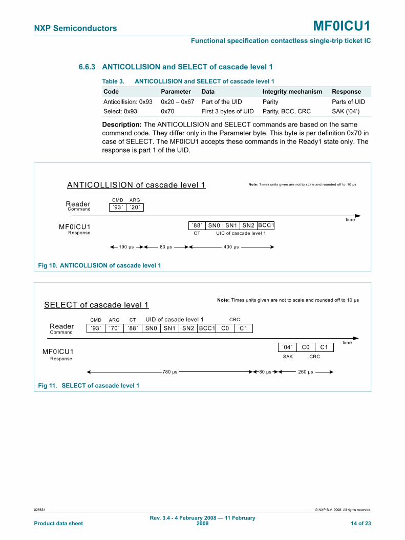
6.6.3 ANTICOLLISION and SELECT of cascade level 1
Description: The ANTICOLLISION and SELECT commands are based on the same command code. They differ only in the Parameter byte. This byte is per definition 0x70 in case of SELECT. The MF0ICU1 accepts these commands in the Ready1 state only. The response is part 1 of the UID.
Table 3. ANTICOLLISION and SELECT of cascade level 1Code Parameter Data Integrity mechanism ResponseAnticollision: 0x93Select: 0x93
0x20 – 0x670x70
Part of the UIDFirst 3 bytes of UID
ParityParity, BCC, CRC
Parts of UIDSAK (‘04’)
Fig 10. ANTICOLLISION of cascade level 1
ReaderCommand
ARG
´88´ SN0 SN1 SN2 BCC1MF0ICU1Response CT UID of cascade level 1
190 µs 80 µs 430 µs
´93´ ´20´CMD
time
Note: Times units given are not to scale and rounded off to 10 µsANTICOLLISION of cascade level 1
Fig 11. SELECT of cascade level 1
ReaderCommand
ARG
´04´ C0 C1
Response SAK CRC
780 µs 80 µs 260 µs
CMD
time
Note: Times units given are not to scale and rounded off to 10 µsSELECT of cascade level 1
´93´ ´70´ ´88´ SN0 SN1 SN2 BCC1 C0 C1UID of casade level 1 CRCCT
MF0ICU1
028634 © NXP B.V. 2008. All rights reserved.
Product data sheetRev. 3.4 - 4 February 2008 — 11 February
2008 14 of 23

NXP Semiconductors MF0ICU1Functional specification contactless single-trip ticket IC
6.6.4 ANTICOLLISION and SELECT of cascade level 2
Description: The ANTICOLLISION and SELECT command are based on the same command code. They differ only in the parameter byte. This byte is per definition 0x70 in case of SELECT. The MF0ICU1 accepts these commands in the Ready2 state only. The response is part 2 of the UID.
Table 4. ANTICOLLISION and SELECT of cascade level 2Code Parameter Data Integrity mechanism ResponseAnticollision: 0x95Select: 0x95
0x20 – 0x670x70
Part of the UIDSecond 4 bytes of UID
ParityParity, BCC, CRC
Parts of UIDSAK (‘00’)
Fig 12. ANTICOLLISION of cascade level 2
ReaderCommand
ARG
SN3 SN4 SN5 SN6 BCC2MF0ICU1Response UID of cascade level 2
190 µs 80 µs 430 µs
´95´ ´20´CMD
time
Note: Times units given are not to scale and rounded off to 10 µsANTICOLLISION of cascade level 2
Fig 13. SELECT of cascade level 2
ReaderCommand
ARG
´00´ C0 C1MF0ICU1
Response SAK CRC
780 µs 80 µs 260 µs
CMD
time
Note: Times units given are not to scale and rounded off to 10 µsSELECT of cascade level 2
´95´ ´70´ SN3 SN4 SN5 SN6 BCC2 C0 C1UID of casade level 1 CRC
028634 © NXP B.V. 2008. All rights reserved.
Product data sheetRev. 3.4 - 4 February 2008 — 11 February
2008 15 of 23

NXP Semiconductors MF0ICU1Functional specification contactless single-trip ticket IC
6.6.5 Read
Description: The READ command needs the page address as a parameter. Only addresses 0x00 to 0X0F are decoded. For higher addresses the MF0 IC U1 returns a NAK. The MF0ICU1 responds to the READ command by sending 16 bytes starting from the page address defined in the command (e.g. if ADR is ‘0x03‘ pages 0x03, 0x04, 0x05, 0x06 are returned). A roll back is implemented; e.g. if ADR is ‘0X0E’, the contents of pages 0X0E, 0X0F, 0x00 and 0x01 is returned).
Table 5. ReadCode Parameter Data Integrity mechanism Response0x30 ADR: 0X00-0X0F - CRC 16 Byte
Date
Fig 14. Read
ReaderCommand
ARG
MF0ICU1Response 16 Byte Data CRC
360 µs80 µs
1540 µs
CMD
time
Note: Times units given are not to scale and rounded off to 10 µsREAD
´30´ ADR C0 C1CRC
D0 D1 D2 ... D13 D14 D15 C0 C1
D0NAK50 µs
028634 © NXP B.V. 2008. All rights reserved.
Product data sheetRev. 3.4 - 4 February 2008 — 11 February
2008 16 of 23

NXP Semiconductors MF0ICU1Functional specification contactless single-trip ticket IC
6.6.6 Halt
Description: The HALT command is used to set already processed MF0 IC U1 devices into a different waiting state (Halt instead of Idle), which allows a simple separation between devices whose UIDs are already known (as they have already passed the anticollision procedure) and devices that have not yet been identified by there UIDs. This mechanism is a very efficient way of finding all contactless devices in the field of a PCD.
6.6.7 Write
Description: The WRITE command is used to program the lock bytes in page 0x02, the OTP bytes in page 0x03 or the data bytes in pages 0X 04 to 0X0F. A WRITE command is performed page-wise, programming 4 bytes in a row.
Table 6. HaltCode Parameter Data Integrity mechanism Response0x50 0x00 - Parity, CRC Passive AK, NAK
Fig 15. Halt
ReaderCommand
ADR
MF0ICU1Response
360 µs 80 µs
CMD
time
Note: Times units given are not to scale and rounded off to 10 µsHALT
´50´ ´00´ C0 C1CRC
D0NAK
50 µs
ACK ---
Table 7. WriteCode Parameter Data Code Parameter0xA2 ADR: 0X00-0X0F 4 Byte 0xA2 ADR: ‘0’ – ‘7’
Fig 16. Write
ReaderCommand
MF0ICU1Response
700 µs 3830 µs
time
Note: Times units given are not to scale and rounded off to 10 µsWRITE
D0NAK50 µs
ARGCMD
´A2´ ADR D0 D1 D2 D3 C0 C14 Byte Data CRC
D0AK
80 µs 50 µs
028634 © NXP B.V. 2008. All rights reserved.
Product data sheetRev. 3.4 - 4 February 2008 — 11 February
2008 17 of 23

NXP Semiconductors MF0ICU1Functional specification contactless single-trip ticket IC
6.6.8 Compatibility write
Description: The COMPATIBILITY WRITE command was implemented to accommodate the established MIFARE PCD infrastructure. Even though 16 bytes are transferred to the MF0ICU1, only the least significant 4 bytes (bytes 0 to 3) will be written to the specified address. It is recommended to set the remaining bytes 0X04 to 0X0F to all ‘0’.
Table 8. Compatibility writeCode Parameter Data Integrity
mechanismResponse
0xA0 ADR: 0X00-0X0F
16 Byte Parity, CRC AK or NAK
Fig 17. Compatibility write
ReaderCommand
MF0ICU1Response
time
Note: Times units given are not to scale and rounded off to 10 µsCOMPATIBILITY WRITE
ARG
´A0´ ADR C0 C1CMD
D0AK
80µs1540 µs
16 Byte Data
D0 ... D15 C0CRC
C1
D0NAK50 µs
360 µs 80 µs 3830 µs
CRC
50 µs
(NAK)
50 µs
028634 © NXP B.V. 2008. All rights reserved.
Product data sheetRev. 3.4 - 4 February 2008 — 11 February
2008 18 of 23

NXP Semiconductors MF0ICU1Functional specification contactless single-trip ticket IC
6.7 Summary of relevant data for device identification
7. Limiting values
See Delivery Type Addendum of Device
8. Recommended operating conditions
See Delivery Type Addendum of Device
9. Characteristics
See Delivery Type Addendum of Device
10. Support information
For additional information, please visit: http://www.nxp.com
11. Package outline
See Delivery Type Addendum of Device
Table 9. Summary of relevant data for device identificationCode Type Value Binary Format RemarkATQA 2 Byte 0x0044 0000 0000 0100
01001st ‘1’ indicates cascade level 22nd ‘1’ indicates MIFARE family
Hard Coded
CT 1 ByteCascade Tag
0x88 1000 1000ensures collision with cascade level 1 products
Hard Coded
SAK (casc. level 1) 1 Byte 0x04 0000 0100‘1’ indicates additional cascade level
Hard Coded
SAK (casc. level 2) 1 Byte 0x00 0000 0000indicates complete UID and MF0 IC U1 functionality
Hard Coded
Manufacturer Byte 1 Byte 0x04 0000 0100indicates manufacturer NXP
Acc. toISO/IEC 14443-3 and ISO/IEC 7816-6 AMD.1
028634 © NXP B.V. 2008. All rights reserved.
Product data sheetRev. 3.4 - 4 February 2008 — 11 February
2008 19 of 23

NXP Semiconductors MF0ICU1Functional specification contactless single-trip ticket IC
12. Revision history
Table 10. Revision historyDocument ID Release date Data sheet status Change notice Supersedes028634 4 February 2008 Product data sheet 3.3
Modifications: • Update• General rewording of MIFARE designation and commercial conditions
028633 July 2008 Product data sheet 3.2
Modifications: • exchange of figure 11 and 13
028632 3 April 2007 Product data sheet 3.1
Modifications: • The format of this data sheet has been redesigned to comply with the new identity guidelines of NXP Semiconductors.
• Legal texts have been adapted to the new company name.
028631 March 2007 Product data sheet 3.0
028630 March 2003 Product data sheet 2.5
028625 March 2003 Write Endurance, Data Retention 2.4
028624 February 2003 Preliminary Version 2.3
028623 January 2003 Include MF0ICU11 type 2.2
028622 January 2003 Updated document layout + wordingChange of Write endurance to 1000 cycles
2.1
028621 January 2003 Introduction of read in state Ready2 and Compatibility write command
2.0
028620 Introduction of Lock bytes and increase of memory to 512 bit. Correction of Manufacturer Code
1.0
028610 First official version
028634 © NXP B.V. 2008. All rights reserved.
Product data sheetRev. 3.4 - 4 February 2008 — 11 February
2008 20 of 23

NXP Semiconductors MF0ICU1Functional specification contactless single-trip ticket IC
13. Legal information
13.1 Data sheet status
[1] Please consult the most recently issued document before initiating or completing a design.
[2] The term ‘short data sheet’ is explained in section “Definitions”.
[3] The product status of device(s) described in this document may have changed since this document was published and may differ in case of multiple devices. The latest product status information is available on the Internet at URL http://www.nxp.com.
13.2 DefinitionsDraft — The document is a draft version only. The content is still under internal review and subject to formal approval, which may result in modifications or additions. NXP Semiconductors does not give any representations or warranties as to the accuracy or completeness of information included herein and shall have no liability for the consequences of use of such information.
Short data sheet — A short data sheet is an extract from a full data sheet with the same product type number(s) and title. A short data sheet is intended for quick reference only and should not be relied upon to contain detailed and full information. For detailed and full information see the relevant full data sheet, which is available on request via the local NXP Semiconductors sales office. In case of any inconsistency or conflict with the short data sheet, the full data sheet shall prevail.
13.3 DisclaimersGeneral — Information in this document is believed to be accurate and reliable. However, NXP Semiconductors does not give any representations or warranties, expressed or implied, as to the accuracy or completeness of such information and shall have no liability for the consequences of use of such information.
Right to make changes — NXP Semiconductors reserves the right to make changes to information published in this document, including without limitation specifications and product descriptions, at any time and without notice. This document supersedes and replaces all information supplied prior to the publication hereof.
Suitability for use — NXP Semiconductors products are not designed, authorized or warranted to be suitable for use in medical, military, aircraft, space or life support equipment, nor in applications where failure or malfunction of a NXP Semiconductors product can reasonably be expected to
result in personal injury, death or severe property or environmental damage. NXP Semiconductors accepts no liability for inclusion and/or use of NXP Semiconductors products in such equipment or applications and therefore such inclusion and/or use is at the customer’s own risk.
Applications — Applications that are described herein for any of these products are for illustrative purposes only. NXP Semiconductors makes no representation or warranty that such applications will be suitable for the specified use without further testing or modification.
Limiting values — Stress above one or more limiting values (as defined in the Absolute Maximum Ratings System of IEC 60134) may cause permanent damage to the device. Limiting values are stress ratings only and operation of the device at these or any other conditions above those given in the Characteristics sections of this document is not implied. Exposure to limiting values for extended periods may affect device reliability.
Terms and conditions of sale — NXP Semiconductors products are sold subject to the general terms and conditions of commercial sale, as published at http://www.nxp.com/profile/terms, including those pertaining to warranty, intellectual property rights infringement and limitation of liability, unless explicitly otherwise agreed to in writing by NXP Semiconductors. In case of any inconsistency or conflict between information in this document and such terms and conditions, the latter will prevail.
No offer to sell or license — Nothing in this document may be interpreted or construed as an offer to sell products that is open for acceptance or the grant, conveyance or implication of any license under any copyrights, patents or other industrial or intellectual property rights.
13.4 TrademarksNotice: All referenced brands, product names, service names and trademarks are the property of their respective owners.
MIFARE — is a trademark of NXP B.V.
14. Contact information
For additional information, please visit: http://www.nxp.com
For sales office addresses, send an email to: [email protected]
Document status[1][2] Product status[3] Definition
Objective [short] data sheet Development This document contains data from the objective specification for product development.
Preliminary [short] data sheet Qualification This document contains data from the preliminary specification.
Product [short] data sheet Production This document contains the product specification.
028634 © NXP B.V. 2008. All rights reserved.
Product data sheetRev. 3.4 - 4 February 2008 — 11 February
2008 21 of 23

NXP Semiconductors MF0ICU1Functional specification contactless single-trip ticket IC
15. Tables
Table 1. REQA . . . . . . . . . . . . . . . . . . . . . . . . . . . . . . . .13Table 2. WUPA . . . . . . . . . . . . . . . . . . . . . . . . . . . . . . . .13Table 3. ANTICOLLISION and SELECT of
cascade level 1 . . . . . . . . . . . . . . . . . . . . . . . . .14Table 4. ANTICOLLISION and SELECT of
cascade level 2 . . . . . . . . . . . . . . . . . . . . . . . . .15Table 5. Read . . . . . . . . . . . . . . . . . . . . . . . . . . . . . . . . .16
Table 6. Halt. . . . . . . . . . . . . . . . . . . . . . . . . . . . . . . . . . 17Table 7. Write. . . . . . . . . . . . . . . . . . . . . . . . . . . . . . . . . 17Table 8. Compatibility write . . . . . . . . . . . . . . . . . . . . . . 18Table 9. Summary of relevant data for device
identification . . . . . . . . . . . . . . . . . . . . . . . . . . . 19Table 10. Revision history . . . . . . . . . . . . . . . . . . . . . . . . 20
16. Figures
Fig 1. MIFARE card reader . . . . . . . . . . . . . . . . . . . . . . .2Fig 2. Block diagram . . . . . . . . . . . . . . . . . . . . . . . . . . . .4Fig 3. Communication principle . . . . . . . . . . . . . . . . . . . .6Fig 4. Memory organization . . . . . . . . . . . . . . . . . . . . . . .9Fig 5. UID/serial number . . . . . . . . . . . . . . . . . . . . . . . .10Fig 6. Lock bytes . . . . . . . . . . . . . . . . . . . . . . . . . . . . . . 11Fig 7. OTP bytes . . . . . . . . . . . . . . . . . . . . . . . . . . . . . .12Fig 8. REQA. . . . . . . . . . . . . . . . . . . . . . . . . . . . . . . . . .13Fig 9. WUPA . . . . . . . . . . . . . . . . . . . . . . . . . . . . . . . . .13Fig 10. ANTICOLLISION of cascade level 1 . . . . . . . . . .14Fig 11. SELECT of cascade level 1 . . . . . . . . . . . . . . . .14Fig 12. ANTICOLLISION of cascade level 2 . . . . . . . . . .15Fig 13. SELECT of cascade level 2 . . . . . . . . . . . . . . . .15Fig 14. Read . . . . . . . . . . . . . . . . . . . . . . . . . . . . . . . . . .16Fig 15. Halt . . . . . . . . . . . . . . . . . . . . . . . . . . . . . . . . . . .17Fig 16. Write. . . . . . . . . . . . . . . . . . . . . . . . . . . . . . . . . . .17Fig 17. Compatibility write . . . . . . . . . . . . . . . . . . . . . . . .18
028634 © NXP B.V. 2008. All rights reserved.
Product data sheetRev. 3.4 - 4 February 2008 — 11 February
2008 22 of 23
continued >>

NXP Semiconductors MF0ICU1Functional specification contactless single-trip ticket IC
17. Contents
1 General description . . . . . . . . . . . . . . . . . . . . . . 11.1 Key applications . . . . . . . . . . . . . . . . . . . . . . . . 11.2 Contactless energy and data transfer. . . . . . . . 11.3 Anticollision. . . . . . . . . . . . . . . . . . . . . . . . . . . . 11.3.1 Cascaded UID . . . . . . . . . . . . . . . . . . . . . . . . . 21.4 Security. . . . . . . . . . . . . . . . . . . . . . . . . . . . . . . 21.5 Delivery options . . . . . . . . . . . . . . . . . . . . . . . . 22 Features . . . . . . . . . . . . . . . . . . . . . . . . . . . . . . . 32.1 MIFARE‚ RF Interface (ISO/IEC 14443 A) . . . . 32.2 EEPROM . . . . . . . . . . . . . . . . . . . . . . . . . . . . . 32.3 Security. . . . . . . . . . . . . . . . . . . . . . . . . . . . . . . 33 Ordering information. . . . . . . . . . . . . . . . . . . . . 34 Block diagram . . . . . . . . . . . . . . . . . . . . . . . . . . 45 Pinning information. . . . . . . . . . . . . . . . . . . . . . 45.1 Pinning . . . . . . . . . . . . . . . . . . . . . . . . . . . . . . . 46 Functional description . . . . . . . . . . . . . . . . . . . 56.1 Block description . . . . . . . . . . . . . . . . . . . . . . . 56.2 Communication principle . . . . . . . . . . . . . . . . . 66.2.1 Idle. . . . . . . . . . . . . . . . . . . . . . . . . . . . . . . . . . 76.2.2 Ready1 . . . . . . . . . . . . . . . . . . . . . . . . . . . . . . . 76.2.3 Ready2 . . . . . . . . . . . . . . . . . . . . . . . . . . . . . . 76.2.4 Active . . . . . . . . . . . . . . . . . . . . . . . . . . . . . . . . 76.2.5 Halt . . . . . . . . . . . . . . . . . . . . . . . . . . . . . . . . . . 86.3 Data integrity. . . . . . . . . . . . . . . . . . . . . . . . . . . 86.4 RF interface . . . . . . . . . . . . . . . . . . . . . . . . . . . 86.5 Memory organization . . . . . . . . . . . . . . . . . . . . 96.5.1 UID/serial number. . . . . . . . . . . . . . . . . . . . . . 106.5.2 Lock bytes . . . . . . . . . . . . . . . . . . . . . . . . . . . 116.5.3 OTP bytes. . . . . . . . . . . . . . . . . . . . . . . . . . . . 126.5.4 Data pages . . . . . . . . . . . . . . . . . . . . . . . . . . . 126.6 Command set . . . . . . . . . . . . . . . . . . . . . . . . . 136.6.1 REQA . . . . . . . . . . . . . . . . . . . . . . . . . . . . . . . 136.6.2 WUPA . . . . . . . . . . . . . . . . . . . . . . . . . . . . . . . 136.6.3 ANTICOLLISION and SELECT of
cascade level 1 . . . . . . . . . . . . . . . . . . . . . . . . 146.6.4 ANTICOLLISION and SELECT of
cascade level 2 . . . . . . . . . . . . . . . . . . . . . . . . 156.6.5 Read . . . . . . . . . . . . . . . . . . . . . . . . . . . . . . . . 166.6.6 Halt . . . . . . . . . . . . . . . . . . . . . . . . . . . . . . . . . 176.6.7 Write . . . . . . . . . . . . . . . . . . . . . . . . . . . . . . . . 176.6.8 Compatibility write. . . . . . . . . . . . . . . . . . . . . . 186.7 Summary of relevant data for device
identification . . . . . . . . . . . . . . . . . . . . . . . . . . 197 Limiting values. . . . . . . . . . . . . . . . . . . . . . . . . 198 Recommended operating conditions. . . . . . . 199 Characteristics. . . . . . . . . . . . . . . . . . . . . . . . . 19
10 Support information . . . . . . . . . . . . . . . . . . . . 1911 Package outline. . . . . . . . . . . . . . . . . . . . . . . . 1912 Revision history . . . . . . . . . . . . . . . . . . . . . . . 2013 Legal information . . . . . . . . . . . . . . . . . . . . . . 2113.1 Data sheet status . . . . . . . . . . . . . . . . . . . . . . 2113.2 Definitions . . . . . . . . . . . . . . . . . . . . . . . . . . . 2113.3 Disclaimers . . . . . . . . . . . . . . . . . . . . . . . . . . 2113.4 Trademarks . . . . . . . . . . . . . . . . . . . . . . . . . . 2114 Contact information . . . . . . . . . . . . . . . . . . . . 2115 Tables . . . . . . . . . . . . . . . . . . . . . . . . . . . . . . . . 2216 Figures . . . . . . . . . . . . . . . . . . . . . . . . . . . . . . . 2217 Contents. . . . . . . . . . . . . . . . . . . . . . . . . . . . . . 23
© NXP B.V. 2008. All rights reserved.For more information, please visit: http://www.nxp.comFor sales office addresses, please send an email to: [email protected]
Date of release: 11 February 2008Document identifier: 028634
Please be aware that important notices concerning this document and the product(s)described herein, have been included in section ‘Legal information’.