maia3 model 2016 brochure - atomika teknik
TRANSCRIPT

MAIA31.0 nm
at 1 keV
newelectroncolumn
UHR SEM
2
The MAIA3 is an ultra-high resolution SEM with excellent imaging capabilities in the whole range of beam energies. A versatile detection system and high spatial resolution allows the observation of even the finest surface details. This is an essential feature for comprehensive characterisation of nanomaterials, for observation of beam-sensitive samples common in the semiconductor industry and for comfortable imaging of non-conductive samples including uncoated biological specimens.
� Triglav™ - a newly designed UHR electron column equipped with the TriLens™ objective and an advanced detection system
� Extraordinary resolution with the UH-resolution lens (60° immersion lens). Completely new high-resolution Analytical lens for field-free analytical work. A re-de-signed Intermediate lens for an extra-large field of view
� Unique combination of crossover-free mode and UH-res-olution lens for outstanding imaging performance
� Traditional TESCAN Wide Field Optics™ design offering a variety of working and display modes
� EquiPower™ for excellent column stability � New Schottky FE gun now enables beam currents up to
400 nA and rapid beam energy changes � Up to 12” wafer SEM inspection by means of extended
chambers and dedicated holders � Triple BSE detection TriBE™ for angle-selective signal
collection. The Mid-Angle BSE and In-Beam LE-BSE de-tectors are located inside the column and detect medi-um-angle and axial backscattered electrons, while the In-Chamber BSE Detector detects wide-angle electrons. Together, they deliver a variety of imaging contrasts and enable low-energy detection down to 200 eV.
� Triple SE detection TriSE™ to capture SE signal optimally in all working modes. The In-Beam SE detector inside the column enables detection of electrons at very short working distances. SE detector for beam deceleration mode gives ultimate resolution in BDM. The In-Chamber SE detector delivers superb topographic contrast.
� Beam Deceleration Technology (BDT) for excellent reso-lution at very low beam energies down to 50 eV (optional)
� Real-time In-Flight Beam Tracing™ for performance and beam optimization
� Extended low-vacuum mode with chamber pressures up to 500 Pa for imaging non-conducting specimens
� Superb ultra-high resolution of 1 nm at 1 keVThe unique combination of immersion optics and crossover-free mode results in extraordinary ultra-high resolution imaging at low energies. The single-pole type objective lens creates a strong magnetic field around the sample and dramatically decreases optical aberrations. Avoiding any crossover in the column reduces the Boersch effect and further optimises the electron beam to yield a superior resolution of 1 nm at 1 keV.
� Imaging at low and ultra-low beam energiesBeam deceleration technology (BDT) consists of the beam deceleration mode (BDM) and high-performance In-Beam detectors for simultaneous SE and BSE signal detection in this mode. In the BDM, the energy of the electrons in the beam is decreased before they impact the surface of the specimen by means of a negative bias voltage which is applied to the sample stage. Ultra-low landing energies down to 50 eV (or 0 eV in manual control) are achievable. BDM enhances the performance of the electron column by reducing optical aberrations, thus allowing small spot sizes and high-resolution imaging at low energies. Low electron energies are advanta-geous for reducing charging effects in non-conductive samples as well as for imaging beam-sensitive and uncoated biological specimens. In this mode, the ultimate resolution is achieved for maximum surface sensitivity and outstanding topographical and material contrast.
MAIA3 Newly designed ultra-high resolution electron column for superb imaging
Key Features

3
TriLens™ - Three lenses, various imaging modesThe TriLens™ objective system is based on the advantageous complementarity of three objective lenses: an UH-resolution lens (60° immersion lens), an Analytical lens and an Intermediate lens (IML). The combination of these lenses results in different working imaging modes.
� UH-RESOLUTION mode This mode is achieved by the unique combination of immersion optics and crossover-free mode for ultra-high resolution imaging at low energies. Avoiding any crossover in the col-umn reduces the Boersch effect and further optimizes the electron beam to yield superior resolution of 1 nm at 1 keV. UHR is ideal for failure analysis in semiconductors, research and characterisation of nanomaterials, non-conductive and very sensitive samples.
� ANALYSIS modeThis mode is implemented by means of the Analytical lens. It is well suited for analysis such as EDS and EBSD, as well as simultaneous SEM imaging during FIB operations such as cross-sectioning and FIB-SEM tomography. High-qual-ity imaging of highly topographic magnetic specimens is possible.
� DEPTH modeThe UH-resolution lens can be used in combination with the IML lens which allows for increasing the probe current while maintaining excellent resolution and enabling large depth of focus. This further extends the analytical capabilities and enables imaging of sensitive samples with high topography.
� OVERVIEW modeThe IML enables a wide field of view.
Triglav™ Experience ultimate resolution
� Key benefits � TriLens™: Objective based on the advantageous comple-
mentarity of three lenses that enables multiple imaging modes � Unique combination of UH-resolution lens with crossover
free mode for superb ultra-high resolution: 1 nm at 1 keV � TriSE™: Three SE detectors to capture the finest surface
details � TriBE™: Three BSE detectors for angle-selective compo-
sitional contrast
� EquiPower™: Excellent column stability ideal for time-con-suming applications such as FIB-SEM tomography
Fig. 1: The TriLens™ objective system. (a) IML (b) Analytical lens
(c) UH-resolution lens
Fig. 2: Resolution test: gold particles on carbon imaged at 50 eV with the SE
(BDM) detector in the UH-RESOLUTION mode.
1
2
100 nm
The new TESCAN SEM column Triglav™ delivers a unique combination of immersion optics and crossover-free mode for UHR imaging at low energies. The single-pole type objective lens creates a magnetic field around the sample and dramatically decreases optical aberrations. Avoiding any crossover in the column reduces the Boersch effect and further optimizes the electron beam to yield superior resolution. Surface details of the specimen can be captured more reliably than ever before. For analysis, the TriLens™ technology improves resolution in the magnetic-field-free mode.
In-Beam SE 0.7 nm at 15 keV
SE (BDM) 1.0 nm at 1 keV
STEM 0.7 nm at 30 keV
IMAGING MODES
� UH-RESOLUTION for the best resolution
� ANALYSIS for analytical techniques
� DEPTH for higher depth of focus
� OVERVIEW for large field of view
4
TriSE™ + TriBE™ - Universal detection systemSee even more with the advanced Triglav™ detection system involving several high-efficiency detectors in the column as well as in the chamber for secondary, back-scattered and transmitted electrons.
TriSE™ – triple SE detection – gives a nearly noise-free comprehensive description of sample topography and allows capturing the finest surface details. Each working mode – whether for ultra-high resolution, analysis or beam deceleration – is equipped with a dedicated SE detector placed in an ideal position with appropriate signal guiding electrodes.
TriBE™ – triple BSE detection – is used to distinguish BSE take-off angles and provides comprehensive information about material composition. A retractable In-Chamber BSE detector placed be-tween the sample and the pole-piece provides both topographic and compositional contrast (from wide-angle electrons) suitable for observation of low-contrast samples. Mid-Angle BSE detec-tor inside the column allows low-noise volume compositional mapping. In-Beam BSE detector captures true compositional information due to pure surface material contrast from axial backscattered electrons.
� TriSE™ – Unique Triple SE detection system � In-Chamber SE
For topographical contrast. � In-Beam SE
For ultra-high resolution and maximum surface sensitivity. � SE (BDM)
For ultimate imaging in the beam deceleration mode (BDM).
� TriBE™ - Unique Triple BSE detection system � In-Chamber BSE (retractable)
For wide-angle BSE detection which provides mainly topo-graphical but also compositional contrast, especially suited for low-contrast samples (e.g. polished samples).
� Mid-angle BSE For medium-angle BSE signal detection which is ideal for imaging at very small WD providing mainly compositional but also topographical contrast.
� In-Beam BSEFor axial BSE detection which provides pure surface ma-terial contrast and best suited for short WD.
Fig. 4: The sophisticated geometry of detector arrangement enables distinguish-
ing BSE take-off angles. (a) In-Beam BSE captures axial BSEs for pure surface Z
contrast. (b) Mid-Angle BSE gives volume Z contrast and (c) In-Chamber BSE
detector provides topographic and compositional contrast.
Fig. 3: See true sample topography. (a) BDM, (b) UH RESOLUTION and (c)
ANALYSIS modes have their own dedicated detectors in ideal positions to
capture fine surface details of the specimen.
3 4
The column excels throughout the entire range of accelerating voltages, however, the highlight is the ultimate resolution at low beam energies which makes this new column ideal for imaging beam-sensitive materials such as:
� low-k dielectric materials � photoresists
� nonconductive materials � uncoated biological specimens
5
� Beam Deceleration Mode When the beam deceleration mode (BDM) is enabled, the detection system allows distinguishing between SE and BSE signals and therefore simultaneous acquisition of both. In this mode, ultimate resolution at low landing energies is achieved for maximum surface sensitivity and outstanding topographical and elemental contrast.
10
Fig. 10: The detection system allows simultaneous acquisition of SE and BSE signals in the beam decel-
eration mode (BDM). (a). The SE (BDM) detector. (b). BSE (BDM) detector. (c). Biased sample.
Fig. 11: Tin balls on carbon imaged in the BDM at 1 keV using the SE (BDM) detector (a) providing topographic
information with typical edge effect and using BSE (BDM) detector (b) giving a compositional information.
� In-Chamber SE
� In-Chamber BSE
� In-Beam SE
� Mid-Angle BSE � In-Beam BSE
Fig. 5-9: SiN with Ag contact imaged at 5 keV with: (5)
The In-Chamber SE detector which delivers excellent
topographic contrast and is less sensitive to charging
(6) The In-Beam SE detector for ultimate resolution
(7) The In-Chamber BSE detector for collecting wide
angle BSE giving topographic and material contrast
(8) The Mid-Angle BSE detector for material contrast
from the whole interaction volume (9) The In-Beam
BSE detector for collecting axial BSE for material
contrast of uppermost surface layers
5 6
7 8 9
11a
11b
10 µm
10 µm
20 µm
20 µm
20 µm
20 µm 20 µm
6
� High Probe Current and Short Analytical WDThe new Schottky FE gun enables beam currents up to 400 nA which are suitable for all analytical techniques such as EDX, WDX, EBSD, CL etc. With the exception of CL, all these detectors are optimised to operate at an analytical working distance of 5 mm, which is short enough to ensure excellent resolution for analysis.
� In-Flight Beam Tracing™Very accurate real-time computation of working distance, magnification and all optical parameters together with continuous control of beam spot size and beam current is ensured by In-Flight Beam Tracing™ technology; a method originally developed by TESCAN.
� EBL with Ultra-Short Dwell Time Down to 20 nsDraw Beam software delivers CADlike drawing of all required shapes and together with ultra-fast scanning provides a flexible tool for fast and efficient e-beam lithography.
� Automated Procedures and User-Friendly SoftwareFast and efficient microscope control with many automated functions (e.g. focusing, stigmation, brightness, beam cen-tring, spot-size optimization, auto-diagnostics) and software extensions (image processing, 3D scanning, correlating position with micrograph or light optical image, etc.) enables truly intuitive user-friendly operation. TESCAN software allows the user - easily or fully automatically - to select the most suitable detector according to the scanning mode.
� MAIA3 configurationsThere are 3 chamber sizes available for MAIA3: LM (large), XM (extra-large) and GM (giant). All MAIA3 chambers provide superior specimen handling using a full 5-axis motorized compucentric stage in ideal geometry for EDX and EBSD. The GM chamber allows the user to observe very large and heavy samples up to a weight of 8 kg (18 lbs). When equipped with a cradle stage and dedicated holders, it can
accommodate 6” and 8” wafers. In addition, the extended GM chamber allows the SEM-imaging of wafers up to 12”.
� CORAL: Correlative Microscopy for Life SciencesCORAL is a powerful software for correlative light-electron microscopy mainly for life sciences. CORAL allows live overlaying of images taken with optical microscopes onto SEM images. This feature makes possible to correlate data from light microscopy with the ultrastructural data obtained by SEM which in turn enables easy navigation on the sample in order to find the region of interest. The SEM stage calibration is designed to be compatible with almost any input device. An automated wizard allows to directly import the images and SEM coordinates from major manufacturers of light microscopes. The collected images can be overlaid in real-time or post-processed within our software.
� Decontaminator OptionSEM observation of specimens at low beam energies tends to be adversely influenced by hydrocarbon contamination. This undesirable deterioration in imaging performance can be significantly reduced by the use of an integrated decontaminator, which is highly recommended option, especially with the use of BDT.
� Load LockLoad Lock is an optional accessory for TESCAN SEMs, which enables quick and easy specimen exchange without the need for disrupting the high vacuum in the SEM chamber. The design of the loading chamber provides the user with the option of exchanging 7 standard stubs at once. The Load Lock is available in two versions - Manual and Automated. The Manual version offers quick, simple and reliable exchange of samples up to 45 mm in diameter. The Automated version adds fully automated control integrated into SEM software and can handle samples of up to 100 mm diameter and wafer sizes up to 4”.
Fig. 12: EBL nanopatterning on a photonic crystal.
Fig. 13: Carbon nanotubes imaged at 500 eV with the SE (BDM) detector.
Fig. 14: Correlative light-electron microscopy with CORAL: Localization of helicobacter pylori in gastric tissue section.
12 13 14
2 µm 200 nm
Features highlights

7
ApplicationsMAIA3 is the ideal choice for imaging non-conductive and beam-sensitive samples including all kinds of biological samples in their natural state. MAIA3 enables highly sensitive surface analysis making it suitable for imaging samples with high topography. It is the SEM sys-tem of choice for keeping up with the increasing demand in all fields of science and technology for high-quality imaging at low beam energies.
� Materials ScienceThe MAIA3 represents a significant advance in the characterisation of nanomaterials. It is also suitable for observation of beam-sensitive and non-conductive samples (e.g. ceram-ics, polymers, glass, fabrics, etc.).
� Semiconductors, optoelectronics and photovoltaicsThe MAIA3 can be effectively used for failure analysis in the semiconduc-tor industry (inspection of integrated circuits, observation of ultra-thin semiconductor sections, solar cells, nanosensors, etc.).
� LithographyThe MAIA3 is a powerful tool for use in the field of electron beam lithography, furthermore is especially suited for imaging sensitive resists, which are prone to high-energy beam damage.
� Life SciencesThe MAIA3 with ultra-high resolu-tion at the lowest beam energy can effectively be used for observation of samples in their natural state without using conductive coatings.
15
17
19
21
16
18
20
22
Fig.: (15-16) Carbon spheres and Ni particles on a nanocrystalline substrate imaged at 2 keV with (15) the In-Beam SE detector for high to-pography contrast, (16) the Mid-Angle BSE detector distinguishes a few Ni nanoparticles for both material and topographical contrast. (17) Silicon substrate with nanocrystalline diamonds with Si vacancies imaged with the In-Beam SE detector which highlights the topography of crystallographic facets. (18) Carbon fibres with silver nanoparticles imaged at 1 keV with the Mid-Angle BSE detector. (19) Pd particles on a C matrix imaged at 1 keV with the Mid-Angle BSE detector for both topography and material contrast. (20) Stained mouse liver at 4 keV with the Mid-angle BSE detector which is ideal for observation of stained biological samples. (21) The tissue of a root imaged at 5 keV with the LE-BSE detector. (22) A sample of mouse cerebellum tissue, fixed, stained and embedded in epoxy imaged at 2 keV with the LE-BSE detector.
1 µm 1 µm
20 µm
5 µm 1 µm
500 nm5 µm
500 nm

8
Imaging of non-conductive samples, detecting nuances of compositional contrast or resolving tiny surface features in many fields of life sciences, materials science or semiconductor engineering have become increasingly important for scanning electron microscopy.With a high energy beam, the penetration depth of the electron beam interacting with the sample surface is high, resulting in a large interaction volume. Modern materials such as very thin - nanometre scale - composites scale cannot be observed at high energies because surface features are transparent to the electron beam. Moreover, thin layers are ordinarily deposited on non-conductive materials (e.g. various types of glass) that make observation of these samples with a high energy electron beam almost impossible. Non-conductive materials and biological samples charge at high accelerating voltages. The detection of low energy backscattered electrons is advantageous for these applications, as charging artefacts are reduced, while surface features are enhanced.Delicate beam-sensitive samples constitute a special category since they are easily prone to radiation damage (caused by the electron beam) and therefore low-energy observation is absolutely necessary.
� TESCAN Low Energy BSE Detectors (LE – BSE)Backscattered electron imaging at low beam energies with high sensitivity and sufficient signal-to-noise ratio are essential features of BSE detectors nowadays. The detection limit of the LE-BSE detector is 200 eV. Its proven high performance at energies under 3 keV makes it the ideal solution for high resolution BSE imaging of surface details and high contrast, clear imaging of sensitive biological samples, or artifact-free imaging of non-conductive materials.
� Common Applications - Charging of Non-conductive SamplesSpecimens such as ceramics, polymers, nano-materials, glass etc. showing charging artifacts that affect secondary electron (SE) detection, can be observed without such distortions when the BSE detector is used. BSE observation at low beam energies results in enhanced specimen surface contrast and more details can be resolved, see Fig. 23. Moreover, the secondary electron signal is more sensitive to thin layers of hydrocarbon contamination on the specimen surface and such contamination can degrade both image quality and the contrast. BSEs are less affected by this negative artifact due to the fact that they have a significantly higher energy (larger escape depth) than secondary electrons.However, with decreasing the primary beam energy, the interaction volume and the escape depth of BSEs get smaller. Thus the detection of low energy BSEs can enhance surface details and increase contrast.
� Material Contrast and Surface DetailsChanges in the primary beam energy result in changes to compositional contrast, see Fig. 24. Keeping the beam at high energy results in loss of detail on the sample surface or a “blurry image”, containing information of deeper layers. Low beam energy observations of various materials such as nano-materials, ceramics, composites or alloys are preferable for such applications.
� Life SciencesBiological samples are particularly sensitive to observation conditions. Precise sample preparation is critical for bio-samples. Such samples suffer from charg-ing effects, and can be also damaged or destroyed by a high energy electron beam. Typical biological samples have very fine surface features, hence coating these specimens with various conductive materials can significantly decrease information content of the acquired image. Tissue and cells are often embedded in non-conductive resins and stained with substances such as osmium in order
Fig.23: Polystyrene balls on Si substrate.
(a) The image acquired at 1 keV by the LE-BSE
detector shows groups of polystyrene balls without
charging artifacts and structure of the substrate.
(b) The image acquired at 3 keV by the LE-BSE
detector exhibits charging effects on the balls,
and because of higher beam energy, substrate
features are not visible. Moreover, at higher energy,
sample damage is evident (some balls are missing
in comparison with the image in 23(a).
23a
23b
Application Example: LE - BSE detector
5 µm
5 µm
9
to enhance contrast. In these cases, working at low primary beam energies and using the LE-BSE detector is nec-essary to obtain clear images without charging effects. Due to lower radiation damage, it is possible to observe the sample in its natural state.
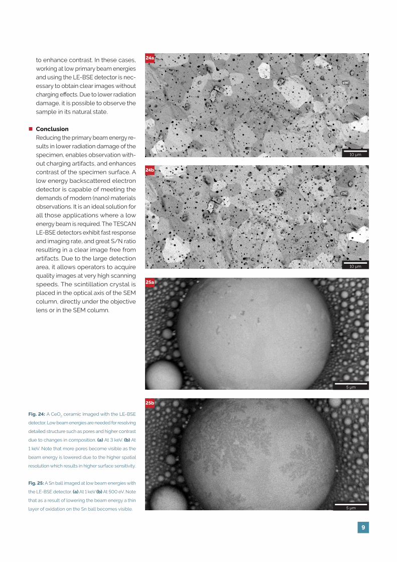
� ConclusionReducing the primary beam energy re-sults in lower radiation damage of the specimen, enables observation with-out charging artifacts, and enhances contrast of the specimen surface. A low energy backscattered electron detector is capable of meeting the demands of modern (nano) materials observations. It is an ideal solution for all those applications where a low energy beam is required. The TESCAN LE-BSE detectors exhibit fast response and imaging rate, and great S/N ratio resulting in a clear image free from artifacts. Due to the large detection area, it allows operators to acquire quality images at very high scanning speeds. The scintillation crystal is placed in the optical axis of the SEM column, directly under the objective lens or in the SEM column.
Fig. 24: A CeO2 ceramic imaged with the LE-BSE
detector. Low beam energies are needed for resolving
detailed structure such as pores and higher contrast
due to changes in composition. (a) At 3 keV. (b) At
1 keV. Note that more pores become visible as the
beam energy is lowered due to the higher spatial
resolution which results in higher surface sensitivity.
Fig. 25: A Sn ball imaged at low beam energies with
the LE-BSE detector. (a) At 1 keV (b) At 500 eV. Note
that as a result of lowering the beam energy a thin
layer of oxidation on the Sn ball becomes visible.
24a
24b
25a
25b
10 µm
10 µm
5 µm
5 µm
10
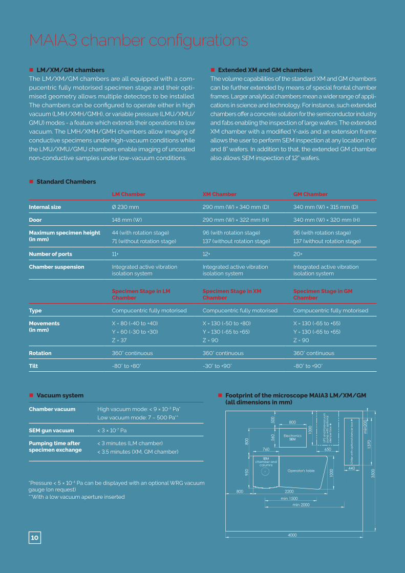
� LM/XM/GM chambersThe LM/XM/GM chambers are all equipped with a com-pucentric fully motorised specimen stage and their opti-mised geometry allows multiple detectors to be installed. The chambers can be configured to operate either in high vacuum (LMH/XMH/GMH), or variable pressure (LMU/XMU/GMU) modes - a feature which extends their operations to low vacuum. The LMH/XMH/GMH chambers allow imaging of conductive specimens under high-vacuum conditions while the LMU/XMU/GMU chambers enable imaging of uncoated non-conductive samples under low-vacuum conditions.
� Extended XM and GM chambers The volume capabilities of the standard XM and GM chambers can be further extended by means of special frontal chamber frames. Larger analytical chambers mean a wider range of appli-cations in science and technology. For instance, such extended chambers offer a concrete solution for the semiconductor industry and fabs enabling the inspection of large wafers. The extended XM chamber with a modified Y-axis and an extension frame allows the user to perform SEM inspection at any location in 6” and 8” wafers. In addition to that, the extended GM chamber also allows SEM inspection of 12” wafers.
LM Chamber XM Chamber GM Chamber
Internal size Ø 230 mm 290 mm (W) × 340 mm (D) 340 mm (W) × 315 mm (D)
Door 148 mm (W) 290 mm (W) × 322 mm (H) 340 mm (W) × 320 mm (H)
Maximum specimen height (in mm)
44 (with rotation stage)
71 (without rotation stage)
96 (with rotation stage)
137 (without rotation stage)
96 (with rotation stage)
137 (without rotation stage)
Number of ports 11+ 12+ 20+
Chamber suspension Integrated active vibration isolation system
Integrated active vibration isolation system
Integrated active vibration isolation system
Specimen Stage in LM Chamber
Specimen Stage in XM Chamber
Specimen Stage in GM Chamber
Type Compucentric fully motorised Compucentric fully motorised Compucentric fully motorised
Movements (in mm)
X = 80 (-40 to +40)
Y = 60 (-30 to +30)
Z = 37
X = 130 (-50 to +80)
Y = 130 (-65 to +65)
Z = 90
X = 130 (-65 to +65)
Y = 130 (-65 to +65)
Z = 90
Rotation 360° continuous 360° continuous 360° continuous
Tilt -80° to +80° -30° to +90° -80° to +90°
Chamber vacuum High vacuum mode: < 9 × 10⁻³ Pa*
Low vacuum mode: 7 – 500 Pa**
SEM gun vacuum < 3 × 10⁻⁷ Pa
Pumping time after specimen exchange
< 3 minutes (LM chamber)
< 3.5 minutes (XM, GM chamber)
� Standard Chambers
*Pressure < 5 × 10⁻⁴ Pa can be displayed with an optional WRG vacuum gauge (on request)**With a low vacuum aperture inserted
� Vacuum system � Footprint of the microscope MAIA3 LM/XM/GM (all dimensions in mm)
MAIA3 chamber configurations
SEM
SEM
11
� Software extensions:
Analysis & Measurement
Histogram
Image Processing
3D Scanning
Hardness
Multi Image Calibrator
Object Area
Switch-Off Timer
Tolerance
X-Positioner
Live Video
EasySEM™
Particles Basic
Particles Advanced
Sample Observer
Image Snapper
DrawBeam Basic
DrawBeam Advanced
3D Metrology (MeX)
System Examiner
Cell Counter
Coral (Correlative microscopy module for Life Sciences)
SYNOPSYS Avalon™ (Correlative microscopy module for semiconductor
standard, option, not available
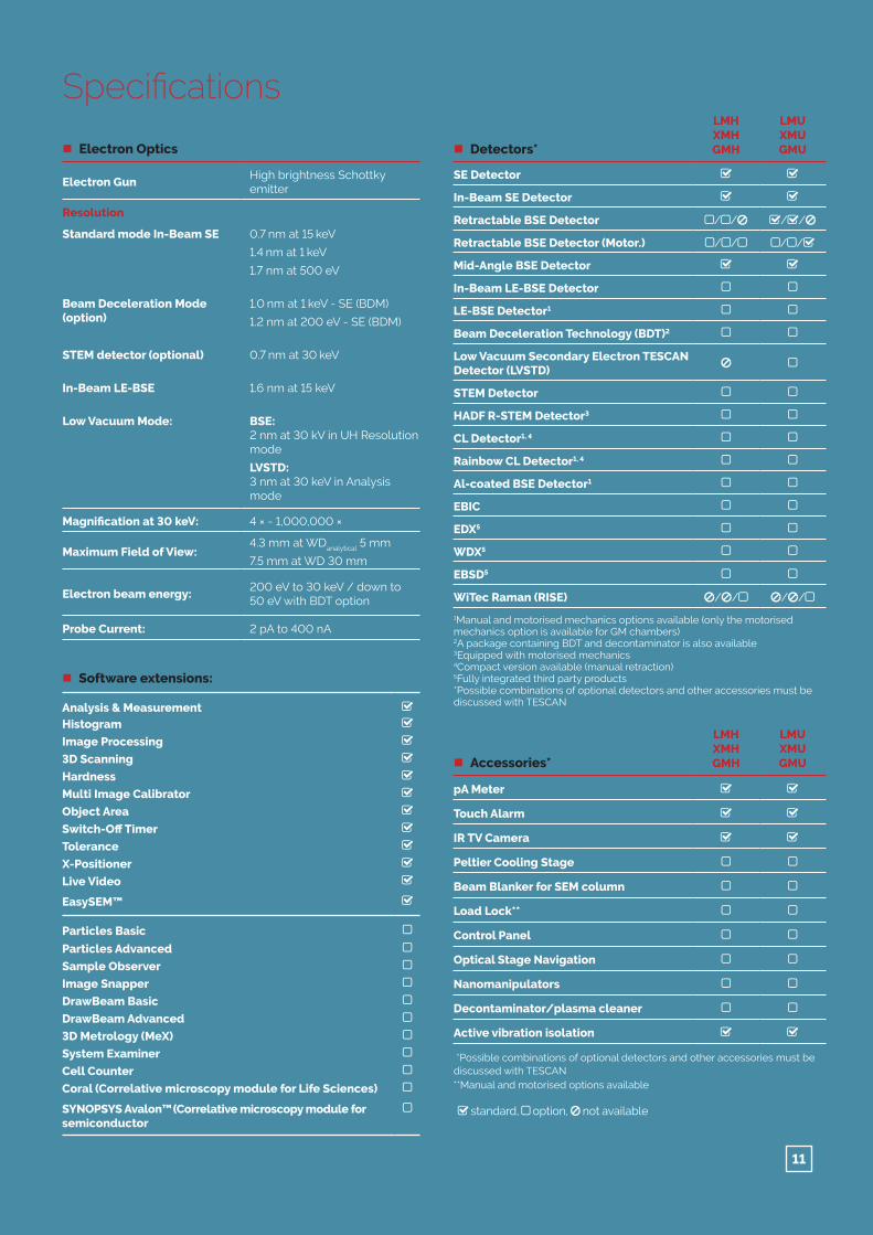
Specifications
� Electron Optics
Electron GunHigh brightness Schottky emitter
Resolution
Standard mode In-Beam SE 0.7 nm at 15 keV
1.4 nm at 1 keV
1.7 nm at 500 eV
Beam Deceleration Mode (option)
1.0 nm at 1 keV - SE (BDM)
1.2 nm at 200 eV - SE (BDM)
STEM detector (optional) 0.7 nm at 30 keV
In-Beam LE-BSE 1.6 nm at 15 keV
Low Vacuum Mode: BSE:2 nm at 30 kV in UH Resolution mode
LVSTD:3 nm at 30 keV in Analysis mode
Magnification at 30 keV: 4 × - 1,000,000 ×
Maximum Field of View: 4.3 mm at WDanalytical 5 mm
7.5 mm at WD 30 mm
Electron beam energy:200 eV to 30 keV / down to 50 eV with BDT option
Probe Current: 2 pA to 400 nA
� Detectors*
LMHXMHGMH
LMUXMUGMU
SE Detector
In-Beam SE Detector
Retractable BSE Detector // //
Retractable BSE Detector (Motor.) // //
Mid-Angle BSE Detector
In-Beam LE-BSE Detector
LE-BSE Detector1
Beam Deceleration Technology (BDT)2
Low Vacuum Secondary Electron TESCAN Detector (LVSTD)
STEM Detector
HADF R-STEM Detector3
CL Detector1, 4
Rainbow CL Detector1, 4
Al-coated BSE Detector1
EBIC
EDX5
WDX5
EBSD5
WiTec Raman (RISE) // //
1Manual and motorised mechanics options available (only the motorised mechanics option is available for GM chambers)2A package containing BDT and decontaminator is also available3Equipped with motorised mechanics4Compact version available (manual retraction) 5Fully integrated third party products*Possible combinations of optional detectors and other accessories must be discussed with TESCAN
� Accessories*
LMHXMHGMH
LMUXMUGMU
pA Meter
Touch Alarm
IR TV Camera
Peltier Cooling Stage
Beam Blanker for SEM column
Load Lock**
Control Panel
Optical Stage Navigation
Nanomanipulators
Decontaminator/plasma cleaner
Active vibration isolation
*Possible combinations of optional detectors and other accessories must be discussed with TESCAN **Manual and motorised options available

www.tescan.com
TESCAN ORSAY HOLDING, a. s.Libušina tř. 21623 00 Brno - KohoutoviceCzech Republic(phone) +420 530 353 411(email) [email protected](email) [email protected]
TE
SC
AN
OR
SA
Y H
OL
DIN
G r
ese
rve
s th
e r
ight
to c
han
ge
th
e d
ocu
me
nt w
itho
ut
no
tice
. 2
017
.06
.08