max86140/max86141 evaluation system - evaluates: … · max86140/max86141 evaluates max86140 and...
TRANSCRIPT
Evaluates: MAX86140 and MAX86141MAX86140/MAX86141 Evaluation System
General DescriptionThe MAX86140/MAX86141 Evaluation System (EVSYS) allows for the quick evaluation of the MAX86140 and MAX86141 optical AFE for applications at various sites on the body, particularly the wrist. Both MAX86140 and MAX86141 supports standard SPI compatible interface. MAX86140 consists of a single optical readout channels, while MAX86141 has two optical readout channels that operate simultaneously. The EVSYS allows flexible configurations to optimize measurement signal quality at minimal power consumption. The EVSYS helps the user quickly learn about how to configure and use the MAX86140 and MAX86141.The EVSYS consists of three boards. MAX32620UC-BLEEK# is the main data acquisition board while MAX86140OSBEK# and MAX86141OSBEK# are the sensor daughter boards for MAX86140 and MAX86141 respectively. The EVSYS can be powered using the USB-C supply or LiPo Battery.The EVSYS comes with a MAX86140ENP+/MAX86141-ENP+ in a 24-bump wafer-level package (WLP).
Features ● Quick Evaluation of the MAX86140/MAX86141 ● Supports Optimization of Configurations ● Facilitates Understanding MAX86140/MAX86141
Architecture and Solution Strategy ● Real-time Monitoring ● Data Logging Capabilities ● On-Board Accelerometer ● Bluetooth LE
319-100050; Rev 0; 8/17
Ordering Information appears at end of data sheet.
Quick StartRequired Equipment
● MAX86140 EVSYS ● Data Acquisition EVSYS Micro-PCB
(MAX32620UCBLEEK#) ● MAX86140 EVSYS Sensor PCB
(MAX86140OSBEK#) ● MAX86141 EVSYS Sensor PCB
(MAX86141OSBEK#) ● Flex cable ● USB-C cable ● MAX86140 EVSYS GUI Software ● MAX86140 Parser and User guide (included in
MAX86140GUISetupVxxx.ZIP) ● Windows PC ● Required Bluetooth LE Dongle CY5677 or CY5670
(not shipped with EVSYS) ● Optional LiPo Battery (LP-401230 suggested, not
shipped with EVSYS)Note: If you do not already have one of the listed BLE dongles above, purchasing one is recommended.
Procedure1) The EVSYS is fully assembled and tested. Follow
the steps below to verify board operation: Visit www.maximintegrated.com/evkit-software to download the most recent version of the EVSYS software, MAX86140GUISetupVxxx_Web.ZIP. Save the EVSYS software to a temporary folder and decompress the ZIP file.
2) Plugged in the BLE dongle to one of the USB port on the PC.
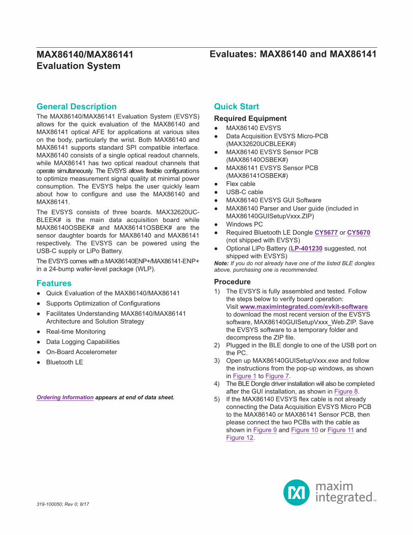
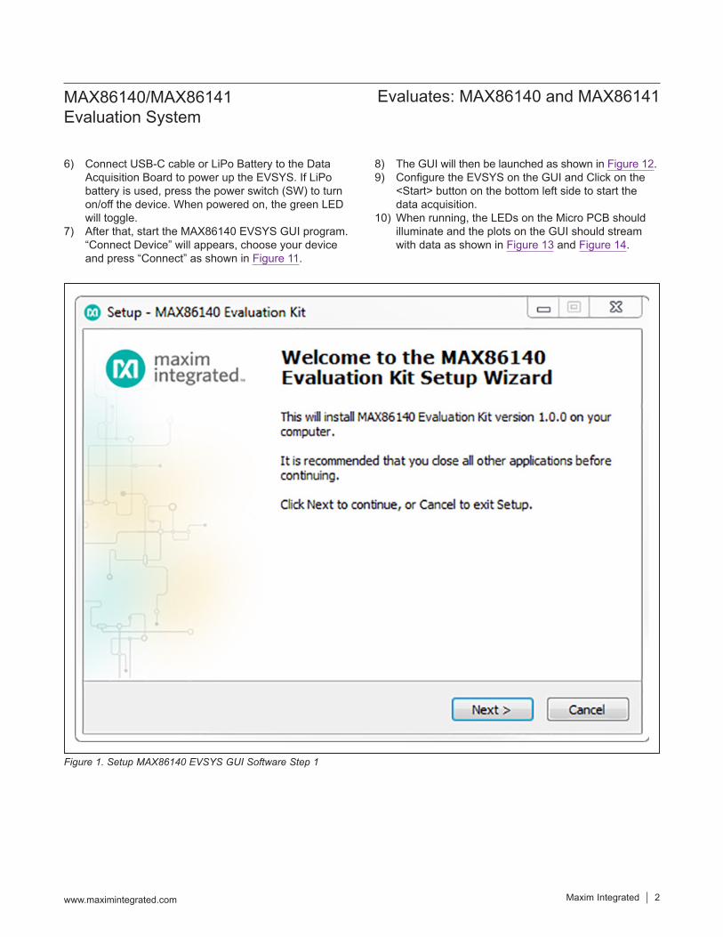
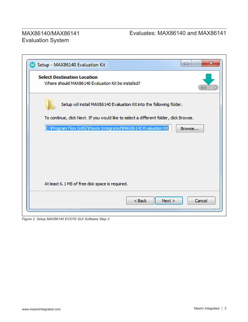
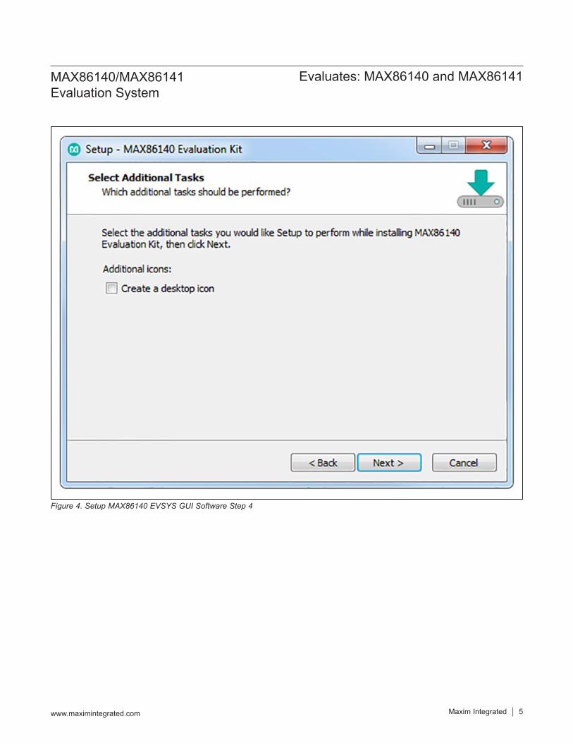
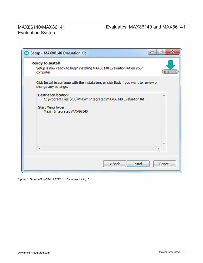
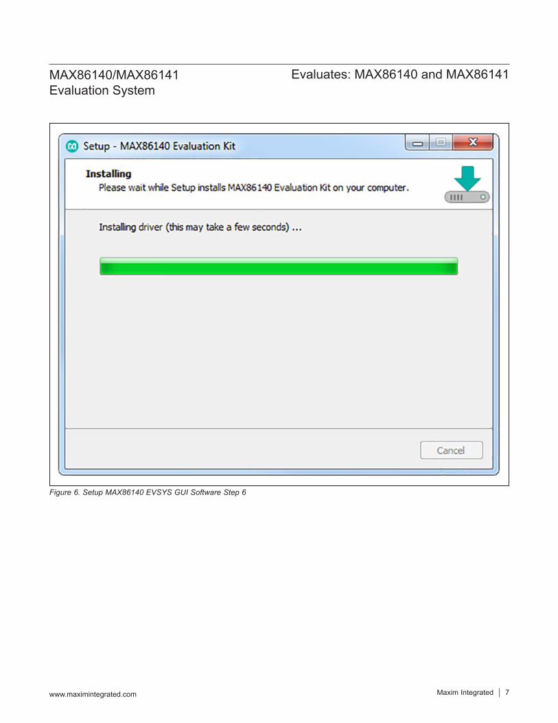
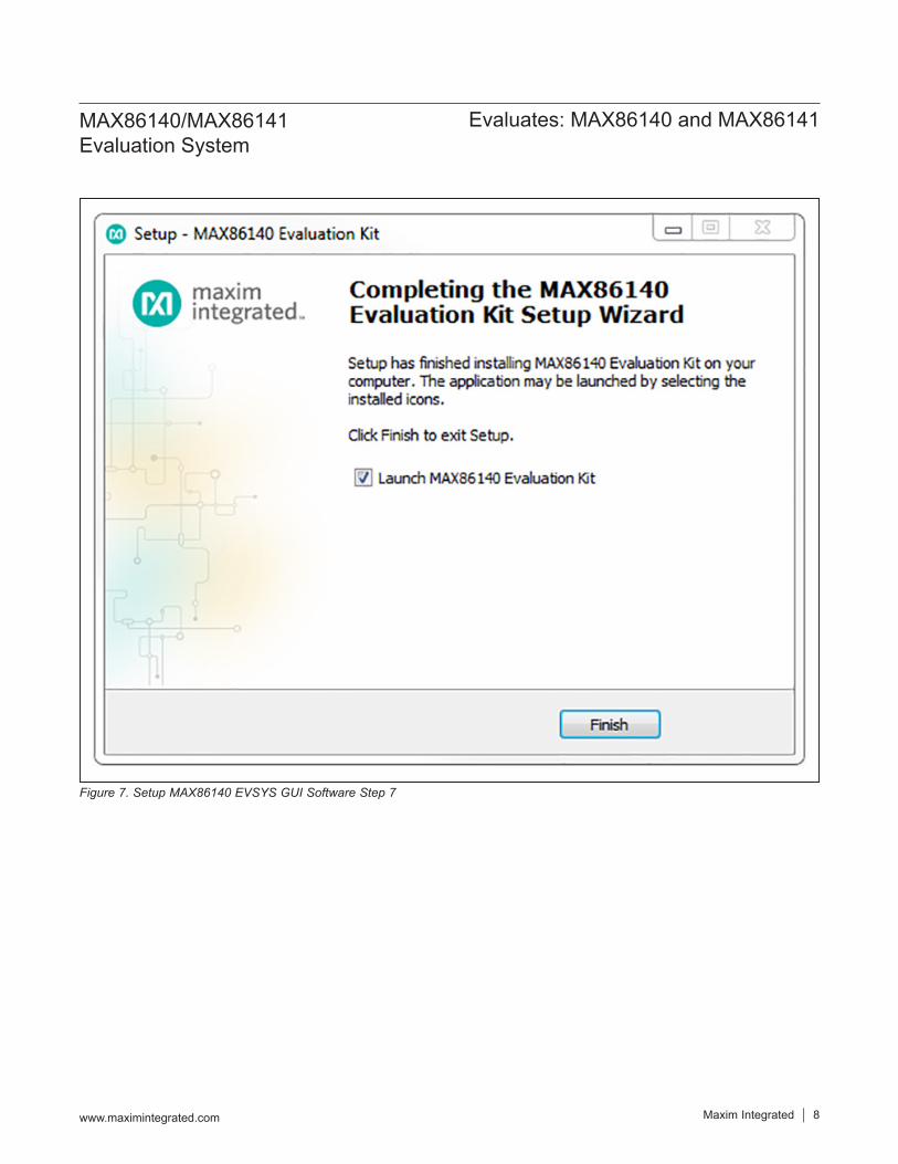
3) Open up MAX86140GUISetupVxxx.exe and follow the instructions from the pop-up windows, as shown in Figure 1 to Figure 7.
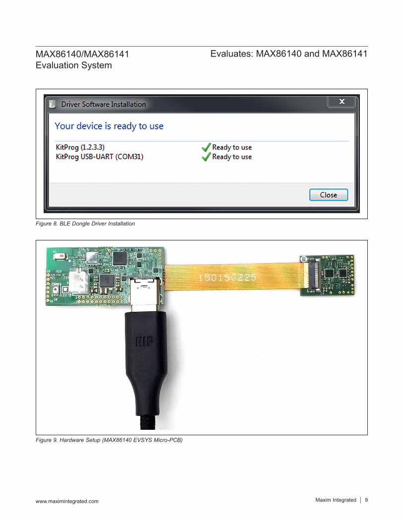
4) The BLE Dongle driver installation will also be completed after the GUI installation, as shown in Figure 8.
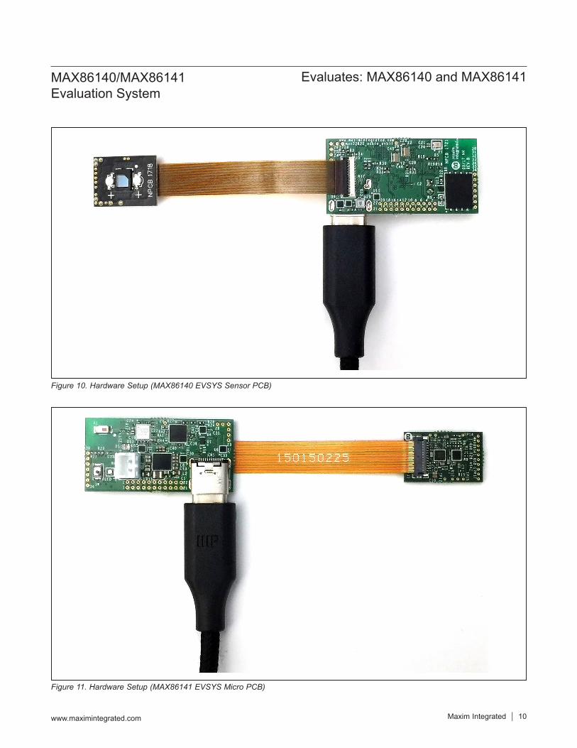
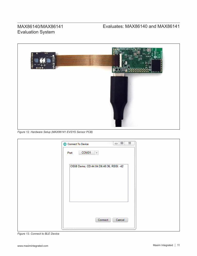
5) If the MAX86140 EVSYS flex cable is not already connecting the Data Acquisition EVSYS Micro PCB to the MAX86140 or MAX86141 Sensor PCB, then please connect the two PCBs with the cable as shown in Figure 9 and Figure 10 or Figure 11 and Figure 12.
Maxim Integrated │ 2www.maximintegrated.com
Evaluates: MAX86140 and MAX86141MAX86140/MAX86141 Evaluation System
6) Connect USB-C cable or LiPo Battery to the Data Acquisition Board to power up the EVSYS. If LiPo battery is used, press the power switch (SW) to turn on/off the device. When powered on, the green LED will toggle.
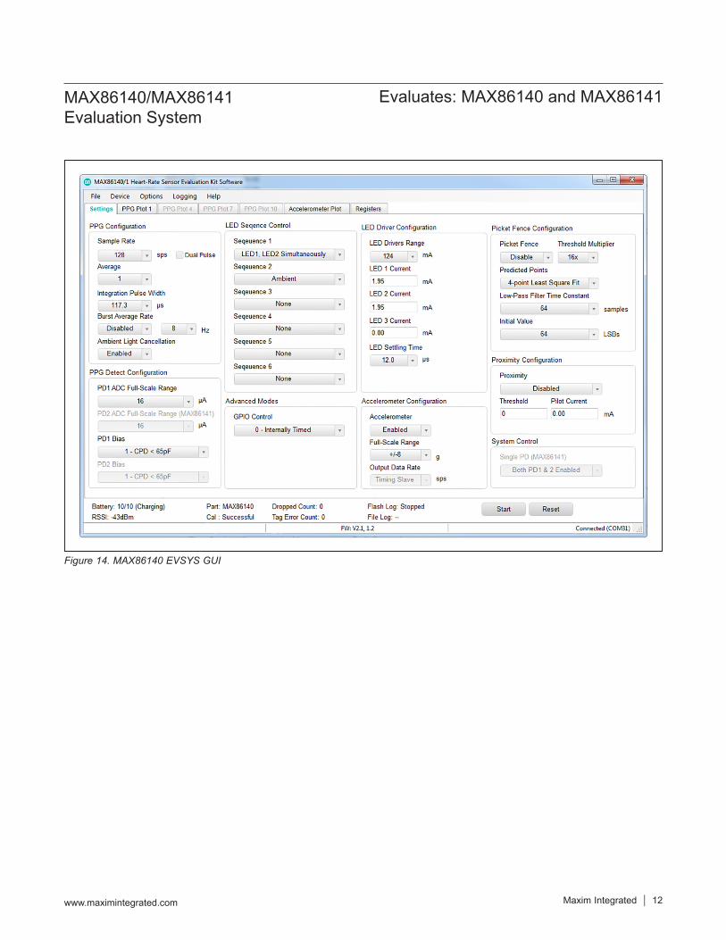
7) After that, start the MAX86140 EVSYS GUI program. “Connect Device” will appears, choose your device and press “Connect” as shown in Figure 11.
8) The GUI will then be launched as shown in Figure 12.9) Configure the EVSYS on the GUI and Click on the
<Start> button on the bottom left side to start the data acquisition.
10) When running, the LEDs on the Micro PCB should illuminate and the plots on the GUI should stream with data as shown in Figure 13 and Figure 14.
Figure 1. Setup MAX86140 EVSYS GUI Software Step 1
Maxim Integrated │ 3www.maximintegrated.com
Evaluates: MAX86140 and MAX86141MAX86140/MAX86141 Evaluation System
Figure 2. Setup MAX86140 EVSYS GUI Software Step 2
Maxim Integrated │ 4www.maximintegrated.com
Evaluates: MAX86140 and MAX86141MAX86140/MAX86141 Evaluation System
Figure 3. Setup MAX86140 EVSYS GUI Software Step 3
Maxim Integrated │ 5www.maximintegrated.com
Evaluates: MAX86140 and MAX86141MAX86140/MAX86141 Evaluation System
Figure 4. Setup MAX86140 EVSYS GUI Software Step 4
Maxim Integrated │ 6www.maximintegrated.com
Evaluates: MAX86140 and MAX86141MAX86140/MAX86141 Evaluation System
Figure 5. Setup MAX86140 EVSYS GUI Software Step 5
Maxim Integrated │ 7www.maximintegrated.com
Evaluates: MAX86140 and MAX86141MAX86140/MAX86141 Evaluation System
Figure 6. Setup MAX86140 EVSYS GUI Software Step 6
Maxim Integrated │ 8www.maximintegrated.com
Evaluates: MAX86140 and MAX86141MAX86140/MAX86141 Evaluation System
Figure 7. Setup MAX86140 EVSYS GUI Software Step 7
Maxim Integrated │ 9www.maximintegrated.com
Evaluates: MAX86140 and MAX86141MAX86140/MAX86141 Evaluation System
Figure 8. BLE Dongle Driver Installation
Figure 9. Hardware Setup (MAX86140 EVSYS Micro-PCB)
Maxim Integrated │ 10www.maximintegrated.com
Evaluates: MAX86140 and MAX86141MAX86140/MAX86141 Evaluation System
Figure 10. Hardware Setup (MAX86140 EVSYS Sensor PCB)
Figure 11. Hardware Setup (MAX86141 EVSYS Micro PCB)
Maxim Integrated │ 11www.maximintegrated.com
Evaluates: MAX86140 and MAX86141MAX86140/MAX86141 Evaluation System
Figure 12. Hardware Setup (MAX86141 EVSYS Sensor PCB)
Figure 13. Connect to BLE Device
Maxim Integrated │ 12www.maximintegrated.com
Evaluates: MAX86140 and MAX86141MAX86140/MAX86141 Evaluation System
Figure 14. MAX86140 EVSYS GUI
Maxim Integrated │ 13www.maximintegrated.com
Evaluates: MAX86140 and MAX86141MAX86140/MAX86141 Evaluation System
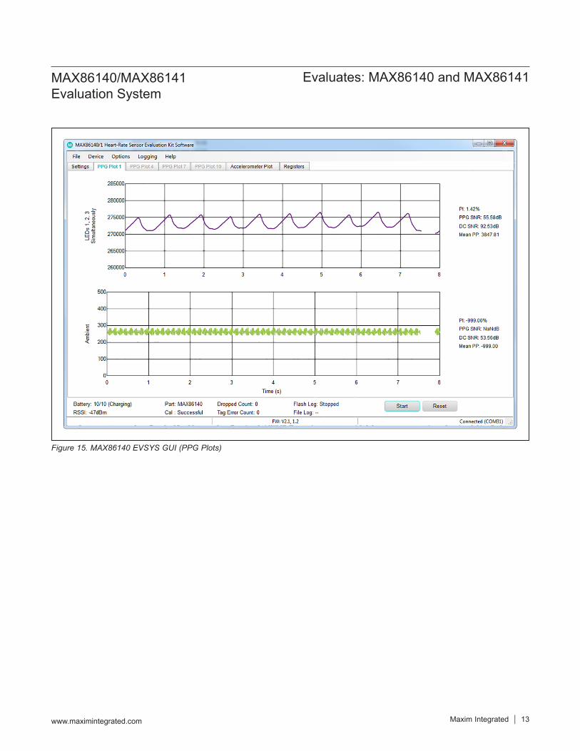
Figure 15. MAX86140 EVSYS GUI (PPG Plots)
Maxim Integrated │ 14www.maximintegrated.com
Evaluates: MAX86140 and MAX86141MAX86140/MAX86141 Evaluation System
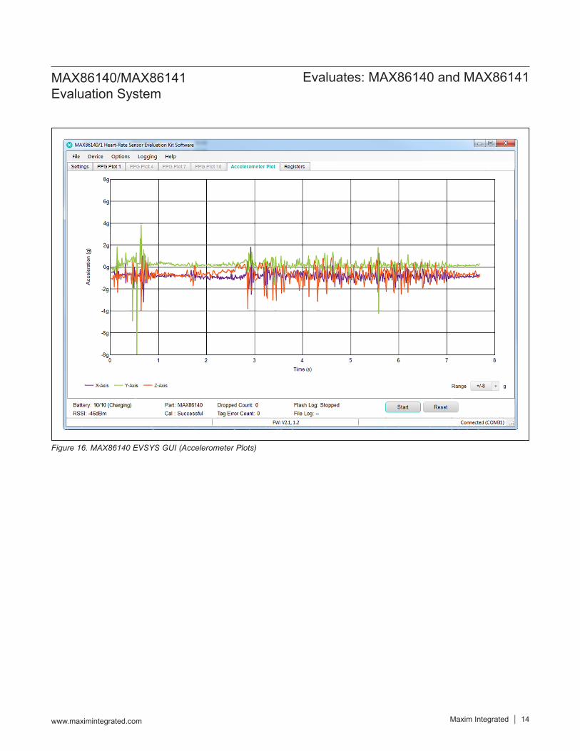
Figure 16. MAX86140 EVSYS GUI (Accelerometer Plots)

Maxim Integrated │ 15www.maximintegrated.com
Evaluates: MAX86140 and MAX86141MAX86140/MAX86141 Evaluation System
Detailed Description of SoftwareThe EVSYS includes two sensor PCB. Each contains MAX86140/MAX86141 optical AFE, a 3-axis acceler-ometer together with two different photodiodes and LEDs. MAX86140_OSB_EVSYS comes with a discreet photodiode (VEMD5010X01) and two green LEDs (LT PWSG-AABB-36-46-F), while MAX86140_OSB_EVSYS comes with two discreet photodiodes (VEMD5010X01), a green LED (LT PWSG-AABB-36-46-F) and an amber LED(Q65111A5283). The EVSYS allows raw optical and accelerometer data to be sampled and transferred to the GUI for both dynamic viewing and logging for later analysis. The EVSYS micro controller PCB is used to do SPI to BLE communication, transporting the raw optical and accelerometer data to the PC via BLE.Most functionality of the MAX86140/MAX86141 has been mapped to the GUI so the wide variety of applications supported by the MAX86140/MAX86141 can be rapidly explored. The following is a brief description of this functionality options.
Sample RateThe sample rate can take on values between 8 to 4096sps. The dual pulse mode option are modes where the samples are unevenly spaced and averaged to improve the ambient rejection of mains line rate ambient signals. Table 1 and Table 2 shows the maximum supported sampling rates (in Sps) for the MAX86140 and MAX86141 respectively for the given number of exposure sequences and use of accelerometer. The maximum sample rate is limited by the BLE protocol, not the AFE itself.For a given sample rate, the number listed can be increased to the next available MAX86140/MAX86141 sample rate (i.e., 500Sps → 512Sps).
Integration Pulse WidthThe pulse width setting adjusts the integration time of an exposure. The MAX86140\MAX86141 supports exposure integration times of 14.8μs, 29.4μs, 58.7μs, and 117.3μs. The exposure pulse width is a critical parameter in any optical measurement. Longer exposures allow for more optical photons to be integrated but also increase system power and reduce ambient rejection capability.
Burst RateWhen Burst Mode is disabled, PPG data conversions are continuous at the sample rate defined by PPG_SR register, When Burst mode is enabled, a burst of PPG data conver-sions occurs at the sample rate defined by Sample Rate
(PPG_SR) register. Number of conversion in the burst is defined by the SMP_AVE register. Average data from the burst of data conversions is pushed to the FIFO at the rate of burst average rate. The burst repeats at the rate of 8, 32, 84, or 256Hz can be configured in burst average field. The burst average rate field defines the rate at which data is pushed into the FIFO. If the number of conversions cannot be accommodated, the device will use the next highest number of conversions. If the effective sample rate is too slow to accommodate the burst rate programmed, BURST_EN is automatically set to 0, and the device runs in continuous mode.
Ambient Light CancellationThe on-chip Ambient Light Cancellation incorporates a proprietary scheme to cancel ambient light generated photo diode current, allowing the sensor to work in high ambient light conditions.
ADC Full-Scale RangeThe MAX86140\MAX86141 optical channel has 4 full-scale ranges. These ranges are 4μA, 8μA, 16μA, and 32μA.
Table 1. MAX86140 Max Sample Rates (Sps)
Table 2. MAX86141 Max Sample Rates (Sps)
ACCELEROMETERWITH WITHOUT
# OF SEQUENCES1 500 1000
2 500 1000
3 250 500
4 250 500
5 125 250
6 125 250
ACCELEROMETERWITH WITHOUT
# OF SEQUENCES1 500 1000
2 250 500
3 125 250
4 125 125
5 125 125
6 62.5 125
Maxim Integrated │ 16www.maximintegrated.com
Evaluates: MAX86140 and MAX86141MAX86140/MAX86141 Evaluation System
Sample AverageThe MAX86140\MAX86141 has the capability to do sample averaging of 2 ~ 128 samples internally. This fea-ture is useful if more optical energy is needed to make a low perfusion measurement but the data rate across the interface or the processing power in a host micro is not desirable. This mode is also useful to further suppress the mains line noises in indoor lighting conditions.
PD BiasThe MAX86140\MAX86141 provides multiple photo diode biasing options. These options allow the MAX86140\MAX86141 to operate with a large range of photo diode capacitance. The PDBIAS values adjust the PD_IN bias point impedance to ensure that the photo diode settles rapidly enough to support the sample timing. PDBIAS is configured depending on the Capacitance (CPD) of the photodiode used.Note: PD2 configuration is only available for MAX86141.
LED Sequence Control (FIFO Time Slots)The LED Sequence Control specifies the data acquisition sequence that the internal state machine controller will follow and where the converted data will be mapped into the FIFO. Each FIFO field can be applied to one measurement. Acquired data can be from LED1, LED2, or LED3 (opti-cal exposure from LED1~3) illuminated independent-ly. The LED1&LED2, LED1&LED3, LED2&LED3, and LED1&LED2&LED3 are optical exposures from LEDs illuminated simultaneously. The other options are Ambient (optical data with no exposure, just ambient illumination) or None (skip this acquisition). The LED4-6 (Mux Control) are not supported with the sensor PCB. If a custom sen-sor board with MUX is used, LED4, LED5 and LED6 can also be configured. Only LED1 and LED2 are available in this EVSYS.The exposure sequence will be the entry in Sequence 1 (LEDC1) slot, Sequence 2 (LEDC 2) slot, Sequence 3 (LEDC3), Sequence 4 (LEDC4), Sequence 5 (LEDC5) slot then Sequence 6 (LEDC6) slot. This sequence will repeat for each sample instance. Each Sequence if pro-grammed, will be plot in the PPG Plot x tabs respectively as shown in Figure 15.Please refer to the MAX86140/MAX86141 datasheet under FIFO Configuration Section for details.
LED Driver ConfigurationsEach of the three LED drivers has a Range and Peak LED Current setting. There are 4 full-scale range settings 31mA, 62mA, 93mA and 124mA. Each range has an 8-bit current source DAC. The Peak LED Current box allows for an actual current to be entered. The nearest available DAC current is selected and displayed in the field.
LED Settling TimeThe LED Settling Time is the time prior to the start of integration (pulse-width setting) that the LED is turned on. There are four settlings, 12μs, 8μs, 6μs and 4μs. This time is necessary to allow the LED driver to settle before integrating the exposure photo current.
GPIO ControlVarious options of GPIO controls are available on MAX86140. For the EVSYS, when set to GPIO options 2, the sample rate will be triggered by the on-board accel-erometer.Please refer to the MAX86140/MAX86141 datasheet under GPIO Configuration Section for details.
Accelerometer ConfigurationThe on-board accelerometer can be enabled or disabled by using the GUI. Supported accelerometer Full-Scale Range are ±2g, ±4g, ±8g and ±16g. The output data of the accelerometer can also be configured from 15.63Hz to 2000Hz when used with GPIO Control Option 2.
Picket Fence ConfigurationUnder typical situations, the rate of change of ambient light is such that the ambient signal level during exposure can be accurately predicted and high levels of ambient rejection are obtained. However, it is possible to have situations where the ambient light level changes extreme-ly rapidly, for example when in a car with direct sunlight exposure passes under a bridge and into a dark shadow. In these situations, it is possible for the on-chip ambient light correction (ALC) circuit to fail and produce and erro-neous estimation of the ambient light during the exposure interval. The optical controller has a built-in algorithm, call the picket fence function, that can correct for these extreme conditions resultant failure of the ALC circuit.Please refer to the MAX86140/MAX86141 datasheet under Picket Fence Detect-and-Replace Function Section for details.

Maxim Integrated │ 17www.maximintegrated.com
Evaluates: MAX86140 and MAX86141MAX86140/MAX86141 Evaluation System
Proximity ConfigurationThe optical controller also includes an optical proxim-ity function which could significantly reduce energy con-sumption and extend battery life when the sensor is not in contact with the skin.Please refer to the MAX86140/MAX86141 datasheet under Proximity Mode Section for details.
System ControlWhen MAX86141 is used, there is option to use single PD (PD1) or Dual PD simultaneously (PD1 and PD2). When Dual PD mode is used, the data log will shows data from both PD for each configured sequence.
<Start >/<Stop > ButtonThe <Start Monitor> button is used to start data acquisi-tion from the demo. The <Start Monitor> button will only be effective when the EVSYS is connected and detected. Once the <Start > has been pushed the <Stop> but-ton appears, which can be used to stop the acquisition. Once the acquisition has started, all settings are locked. Terminate the acquisition to change any settling.
<Reset> ButtonThe <Reset> button will clear out all register settlings back to the programs start up.
Data LoggingRaw optical and accelerometer data can be logged from the <Logging> pull-down menu item. There are two options available: Data saved to file or in the flash. When “file” data logging is selected, the GUI asks for a folder location where the logging file will be saved. Create a new folder or accept the default. Data logging will start on the next <Start> button and will continue until the <Stop > button is pressed. The final file write is only done when the <File> pull-down menu item is accessed and the data-logging button is pressed.
Flash logging allows raw sensor data to be stored to the integrated 32MB flash memory chip in a binary file format. The max duration for flash logging is dependent on: sample rate, number of optical channels, and use of accelerometer. The GUI enables/disables flash logging. The GUI can be disconnected while flash logging, allowing for remote operation (PPG Plots not available). Preparing the flash memory can take up to 30s after enabling. If the flash memory fills or battery power drops too low, flash logging will automatically stop and the file will close. Only one file can be saved at a time. The file must be downloaded since it will be erased on the next log request.If a log has completed, a binary file will be found on the device. The binary log file must be downloaded via the USB-C cable; it cannot be downloaded through BLE. When the device is plugged into the PC, it enumerates as a USB mass storage device. However, the file can only be copied from this device. No other operations (such as deleting or saving other files) will work on this device. Copy the file to a local PC volume. Then run the parser to generate a CSV file.Please refer to the Evaluation Kit Parser User Guide (max8614x demo + eval kit parser user guide 20170719.pdf) for details operation.
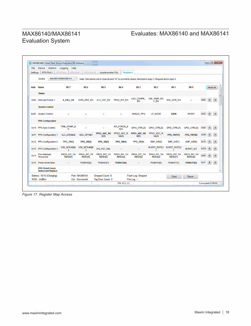
Register Map AccessUnder the <Register> Tab the user can access to sensor register map as shown in Figure 15. Press <Read All>, to read all the register value currently in configured in the Optical AFE. Bolded font bits are logic one. Normal font bits are logic zero. Click on the bits to toggle their value and click on <W> to write the value to the device. The register value does not change until <W> is clicked. Click <R> to read the register value to verify the write.
Maxim Integrated │ 18www.maximintegrated.com
Evaluates: MAX86140 and MAX86141MAX86140/MAX86141 Evaluation System
Figure 17. Register Map Access
Maxim Integrated │ 19www.maximintegrated.com
Evaluates: MAX86140 and MAX86141MAX86140/MAX86141 Evaluation System
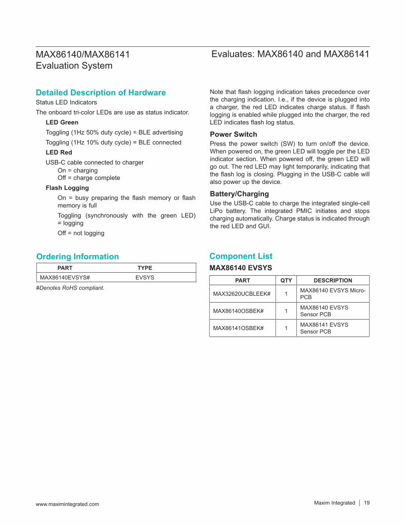
Detailed Description of HardwareStatus LED IndicatorsThe onboard tri-color LEDs are use as status indicator.
LED GreenToggling (1Hz 50% duty cycle) = BLE advertisingToggling (1Hz 10% duty cycle) = BLE connectedLED RedUSB-C cable connected to charger
On = chargingOff = charge complete
Flash LoggingOn = busy preparing the flash memory or flash memory is fullToggling (synchronously with the green LED) = loggingOff = not logging
Note that flash logging indication takes precedence over the charging indication. I.e., if the device is plugged into a charger, the red LED indicates charge status. If flash logging is enabled while plugged into the charger, the red LED indicates flash log status.
Power SwitchPress the power switch (SW) to turn on/off the device. When powered on, the green LED will toggle per the LED indicator section. When powered off, the green LED will go out. The red LED may light temporarily, indicating that the flash log is closing. Plugging in the USB-C cable will also power up the device.
Battery/ChargingUse the USB-C cable to charge the integrated single-cell LiPo battery. The integrated PMIC initiates and stops charging automatically. Charge status is indicated through the red LED and GUI.
#Denotes RoHS compliant.
Component ListMAX86140 EVSYS
Ordering Information
PART QTY DESCRIPTION
MAX32620UCBLEEK# 1 MAX86140 EVSYS Micro-PCB
MAX86140OSBEK# 1 MAX86140 EVSYS Sensor PCB
MAX86141OSBEK# 1 MAX86141 EVSYS Sensor PCB
PART TYPEMAX86140EVSYS# EVSYS
Maxim Integrated │ 20www.maximintegrated.com
Evaluates: MAX86140 and MAX86141MAX86140/MAX86141 Evaluation System
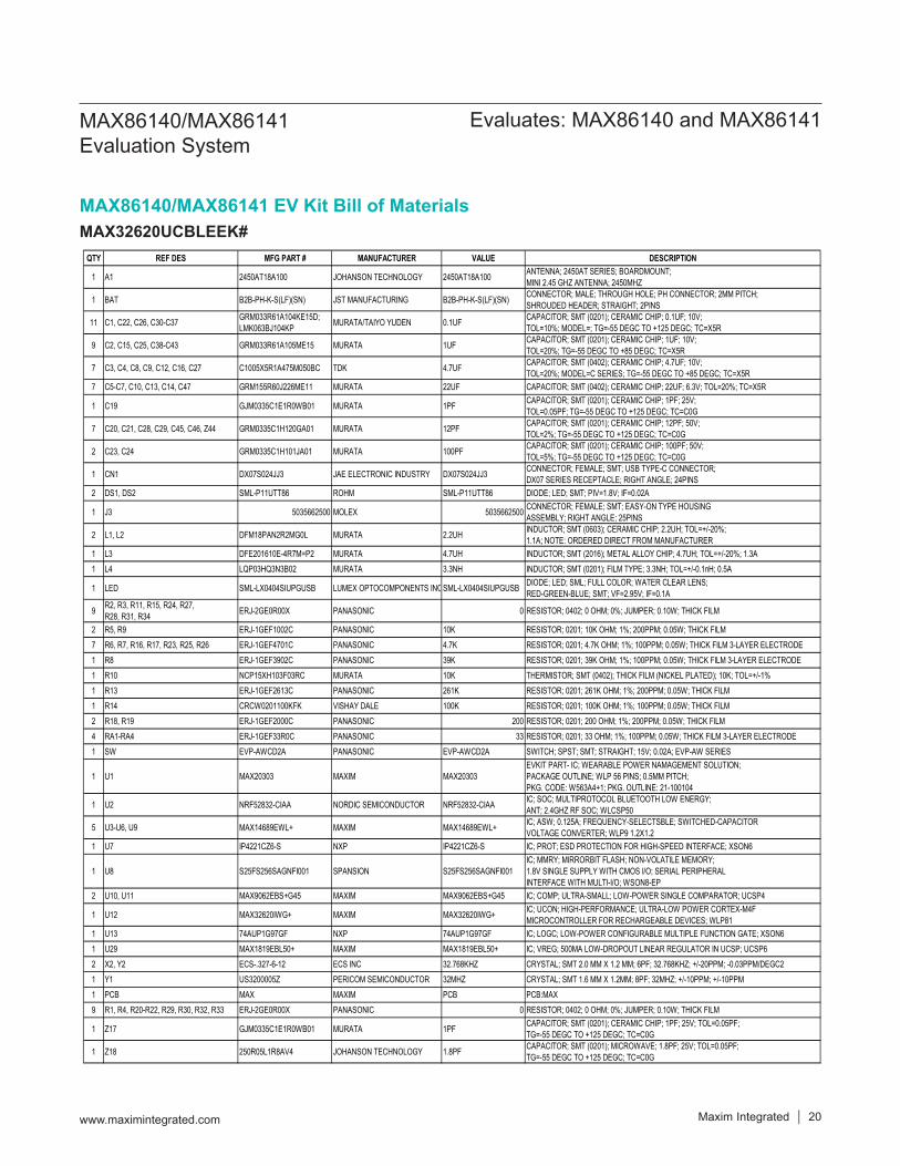
MAX86140/MAX86141 EV Kit Bill of MaterialsMAX32620UCBLEEK#
QTY REF DES MFG PART # MANUFACTURER VALUE DESCRIPTION
1 A1 2450AT18A100 JOHANSON TECHNOLOGY 2450AT18A100 ANTENNA; 2450AT SERIES; BOARDMOUNT; MINI 2.45 GHZ ANTENNA; 2450MHZ
1 BAT B2B-PH-K-S(LF)(SN) JST MANUFACTURING B2B-PH-K-S(LF)(SN) CONNECTOR; MALE; THROUGH HOLE; PH CONNECTOR; 2MM PITCH; SHROUDED HEADER; STRAIGHT; 2PINS
11 C1, C22, C26, C30-C37 GRM033R61A104KE15D; LMK063BJ104KP MURATA/TAIYO YUDEN 0.1UF CAPACITOR; SMT (0201); CERAMIC CHIP; 0.1UF; 10V;
TOL=10%; MODEL=; TG=-55 DEGC TO +125 DEGC; TC=X5R
9 C2, C15, C25, C38-C43 GRM033R61A105ME15 MURATA 1UF CAPACITOR; SMT (0201); CERAMIC CHIP; 1UF; 10V; TOL=20%; TG=-55 DEGC TO +85 DEGC; TC=X5R
7 C3, C4, C8, C9, C12, C16, C27 C1005X5R1A475M050BC TDK 4.7UF CAPACITOR; SMT (0402); CERAMIC CHIP; 4.7UF; 10V; TOL=20%; MODEL=C SERIES; TG=-55 DEGC TO +85 DEGC; TC=X5R
7 C5-C7, C10, C13, C14, C47 GRM155R60J226ME11 MURATA 22UF CAPACITOR; SMT (0402); CERAMIC CHIP; 22UF; 6.3V; TOL=20%; TC=X5R
1 C19 GJM0335C1E1R0WB01 MURATA 1PF CAPACITOR; SMT (0201); CERAMIC CHIP; 1PF; 25V; TOL=0.05PF; TG=-55 DEGC TO +125 DEGC; TC=C0G
7 C20, C21, C28, C29, C45, C46, Z44 GRM0335C1H120GA01 MURATA 12PF CAPACITOR; SMT (0201); CERAMIC CHIP; 12PF; 50V; TOL=2%; TG=-55 DEGC TO +125 DEGC; TC=C0G
2 C23, C24 GRM0335C1H101JA01 MURATA 100PF CAPACITOR; SMT (0201); CERAMIC CHIP; 100PF; 50V; TOL=5%; TG=-55 DEGC TO +125 DEGC; TC=C0G
1 CN1 DX07S024JJ3 JAE ELECTRONIC INDUSTRY DX07S024JJ3 CONNECTOR; FEMALE; SMT; USB TYPE-C CONNECTOR; DX07 SERIES RECEPTACLE; RIGHT ANGLE; 24PINS
2 DS1, DS2 SML-P11UTT86 ROHM SML-P11UTT86 DIODE; LED; SMT; PIV=1.8V; IF=0.02A
1 J3 5035662500 MOLEX 5035662500 CONNECTOR; FEMALE; SMT; EASY-ON TYPE HOUSING ASSEMBLY; RIGHT ANGLE; 25PINS
2 L1, L2 DFM18PAN2R2MG0L MURATA 2.2UH INDUCTOR; SMT (0603); CERAMIC CHIP; 2.2UH; TOL=+/-20%; 1.1A; NOTE: ORDERED DIRECT FROM MANUFACTURER
1 L3 DFE201610E-4R7M=P2 MURATA 4.7UH INDUCTOR; SMT (2016); METAL ALLOY CHIP; 4.7UH; TOL=+/-20%; 1.3A
1 L4 LQP03HQ3N3B02 MURATA 3.3NH INDUCTOR; SMT (0201); FILM TYPE; 3.3NH; TOL=+/-0.1nH; 0.5A
1 LED SML-LX0404SIUPGUSB LUMEX OPTOCOMPONENTS INCSML-LX0404SIUPGUSB DIODE; LED; SML; FULL COLOR; WATER CLEAR LENS; RED-GREEN-BLUE; SMT; VF=2.95V; IF=0.1A
9 R2, R3, R11, R15, R24, R27, R28, R31, R34 ERJ-2GE0R00X PANASONIC 0 RESISTOR; 0402; 0 OHM; 0%; JUMPER; 0.10W; THICK FILM
2 R5, R9 ERJ-1GEF1002C PANASONIC 10K RESISTOR; 0201; 10K OHM; 1%; 200PPM; 0.05W; THICK FILM
7 R6, R7, R16, R17, R23, R25, R26 ERJ-1GEF4701C PANASONIC 4.7K RESISTOR; 0201; 4.7K OHM; 1%; 100PPM; 0.05W; THICK FILM 3-LAYER ELECTRODE
1 R8 ERJ-1GEF3902C PANASONIC 39K RESISTOR; 0201; 39K OHM; 1%; 100PPM; 0.05W; THICK FILM 3-LAYER ELECTRODE
1 R10 NCP15XH103F03RC MURATA 10K THERMISTOR; SMT (0402); THICK FILM (NICKEL PLATED); 10K; TOL=+/-1%
1 R13 ERJ-1GEF2613C PANASONIC 261K RESISTOR; 0201; 261K OHM; 1%; 200PPM; 0.05W; THICK FILM
1 R14 CRCW0201100KFK VISHAY DALE 100K RESISTOR; 0201; 100K OHM; 1%; 100PPM; 0.05W; THICK FILM
2 R18, R19 ERJ-1GEF2000C PANASONIC 200 RESISTOR; 0201; 200 OHM; 1%; 200PPM; 0.05W; THICK FILM
4 RA1-RA4 ERJ-1GEF33R0C PANASONIC 33 RESISTOR; 0201; 33 OHM; 1%; 100PPM; 0.05W; THICK FILM 3-LAYER ELECTRODE
1 SW EVP-AWCD2A PANASONIC EVP-AWCD2A SWITCH; SPST; SMT; STRAIGHT; 15V; 0.02A; EVP-AW SERIES
1 U1 MAX20303 MAXIM MAX20303EVKIT PART- IC; WEARABLE POWER NAMAGEMENT SOLUTION; PACKAGE OUTLINE; WLP 56 PINS; 0.5MM PITCH; PKG. CODE: W563A4+1; PKG. OUTLINE: 21-100104
1 U2 NRF52832-CIAA NORDIC SEMICONDUCTOR NRF52832-CIAA IC; SOC; MULTIPROTOCOL BLUETOOTH LOW ENERGY; ANT; 2.4GHZ RF SOC; WLCSP50
5 U3-U6, U9 MAX14689EWL+ MAXIM MAX14689EWL+ IC; ASW; 0.125A; FREQUENCY-SELECTSBLE; SWITCHED-CAPACITOR VOLTAGE CONVERTER; WLP9 1.2X1.2
1 U7 IP4221CZ6-S NXP IP4221CZ6-S IC; PROT; ESD PROTECTION FOR HIGH-SPEED INTERFACE; XSON6
1 U8 S25FS256SAGNFI001 SPANSION S25FS256SAGNFI001IC; MMRY; MIRRORBIT FLASH; NON-VOLATILE MEMORY; 1.8V SINGLE SUPPLY WITH CMOS I/O; SERIAL PERIPHERAL INTERFACE WITH MULTI-I/O; WSON8-EP
2 U10, U11 MAX9062EBS+G45 MAXIM MAX9062EBS+G45 IC; COMP; ULTRA-SMALL; LOW-POWER SINGLE COMPARATOR; UCSP4
1 U12 MAX32620IWG+ MAXIM MAX32620IWG+ IC; UCON; HIGH-PERFORMANCE; ULTRA-LOW POWER CORTEX-M4F MICROCONTROLLER FOR RECHARGEABLE DEVICES; WLP81
1 U13 74AUP1G97GF NXP 74AUP1G97GF IC; LOGC; LOW-POWER CONFIGURABLE MULTIPLE FUNCTION GATE; XSON6
1 U29 MAX1819EBL50+ MAXIM MAX1819EBL50+ IC; VREG; 500MA LOW-DROPOUT LINEAR REGULATOR IN UCSP; UCSP6
2 X2, Y2 ECS-.327-6-12 ECS INC 32.768KHZ CRYSTAL; SMT 2.0 MM X 1.2 MM; 6PF; 32.768KHZ; +/-20PPM; -0.03PPM/DEGC2
1 Y1 US3200005Z PERICOM SEMICONDUCTOR 32MHZ CRYSTAL; SMT 1.6 MM X 1.2MM; 8PF; 32MHZ; +/-10PPM; +/-10PPM
1 PCB MAX MAXIM PCB PCB:MAX
9 R1, R4, R20-R22, R29, R30, R32, R33 ERJ-2GE0R00X PANASONIC 0 RESISTOR; 0402; 0 OHM; 0%; JUMPER; 0.10W; THICK FILM
1 Z17 GJM0335C1E1R0WB01 MURATA 1PF CAPACITOR; SMT (0201); CERAMIC CHIP; 1PF; 25V; TOL=0.05PF; TG=-55 DEGC TO +125 DEGC; TC=C0G
1 Z18 250R05L1R8AV4 JOHANSON TECHNOLOGY 1.8PF CAPACITOR; SMT (0201); MICROWAVE; 1.8PF; 25V; TOL=0.05PF; TG=-55 DEGC TO +125 DEGC; TC=C0G
Maxim Integrated │ 21www.maximintegrated.com
Evaluates: MAX86140 and MAX86141MAX86140/MAX86141 Evaluation System
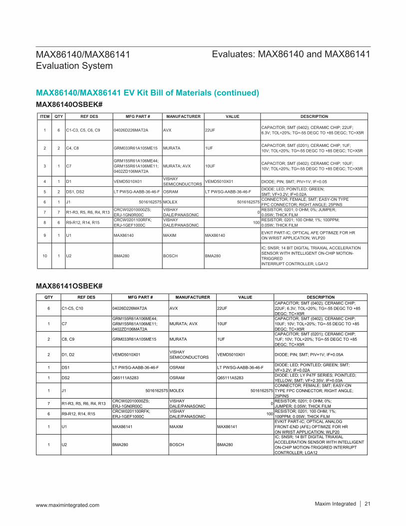
MAX86140/MAX86141 EV Kit Bill of Materials (continued)MAX86140OSBEK#
MAX86141OSBEK#
ITEM QTY REF DES MFG PART # MANUFACTURER VALUE DESCRIPTION
1 6 C1-C3, C5, C6, C9 04026D226MAT2A AVX 22UF CAPACITOR; SMT (0402); CERAMIC CHIP; 22UF; 6.3V; TOL=20%; TG=-55 DEGC TO +85 DEGC; TC=X5R
2 2 C4, C8 GRM033R61A105ME15 MURATA 1UF CAPACITOR; SMT (0201); CERAMIC CHIP; 1UF; 10V; TOL=20%; TG=-55 DEGC TO +85 DEGC; TC=X5R
3 1 C7GRM155R61A106ME44; GRM155R61A106ME11; 0402ZD106MAT2A
MURATA; AVX 10UF CAPACITOR; SMT (0402); CERAMIC CHIP; 10UF; 10V; TOL=20%; TG=-55 DEGC TO +85 DEGC; TC=X5R
4 1 D1 VEMD5010X01 VISHAY SEMICONDUCTORS VEMD5010X01 DIODE; PIN; SMT; PIV=1V; IF=0.05
5 2 DS1, DS2 LT PWSG-AABB-36-46-F OSRAM LT PWSG-AABB-36-46-F DIODE; LED; POINTLED; GREEN; SMT; VF=3.2V; IF=0.02A
6 1 J1 5016162575 MOLEX 5016162575 CONNECTOR; FEMALE; SMT; EASY-ON TYPE FPC CONNECTOR; RIGHT ANGLE; 25PINS
7 7 R1-R3, R5, R6, R4, R13 CRCW02010000ZS; ERJ-1GN0R00C
VISHAY DALE/PANASONIC 0 RESISTOR; 0201; 0 OHM; 0%; JUMPER;
0.05W; THICK FILM
8 6 R9-R12, R14, R15 CRCW0201100RFK; ERJ-1GEF1000C
VISHAY DALE/PANASONIC 100 RESISTOR; 0201; 100 OHM; 1%; 100PPM;
0.05W; THICK FILM
9 1 U1 MAX86140 MAXIM MAX86140 EVKIT PART-IC; OPTICAL AFE OPTIMIZE FOR HR ON WRIST APPLICATION; WLP20
10 1 U2 BMA280 BOSCH BMA280
IC; SNSR; 14 BIT DIGITAL TRIAXIAL ACCELERATION SENSOR WITH INTELLIGENT ON-CHIP MOTION-TRIGGRED INTERRUPT CONTROLLER; LGA12
QTY REF DES MFG PART # MANUFACTURER VALUE DESCRIPTION
6 C1-C5, C10 04026D226MAT2A AVX 22UFCAPACITOR; SMT (0402); CERAMIC CHIP; 22UF; 6.3V; TOL=20%; TG=-55 DEGC TO +85 DEGC; TC=X5R
1 C7GRM155R61A106ME44; GRM155R61A106ME11; 0402ZD106MAT2A
MURATA; AVX 10UFCAPACITOR; SMT (0402); CERAMIC CHIP; 10UF; 10V; TOL=20%; TG=-55 DEGC TO +85 DEGC; TC=X5R
2 C8, C9 GRM033R61A105ME15 MURATA 1UFCAPACITOR; SMT (0201); CERAMIC CHIP; 1UF; 10V; TOL=20%; TG=-55 DEGC TO +85 DEGC; TC=X5R
2 D1, D2 VEMD5010X01 VISHAY SEMICONDUCTORS VEMD5010X01 DIODE; PIN; SMT; PIV=1V; IF=0.05A
1 DS1 LT PWSG-AABB-36-46-F OSRAM LT PWSG-AABB-36-46-F DIODE; LED; POINTLED; GREEN; SMT; VF=3.2V; IF=0.02A
1 DS2 Q65111A5283 OSRAM Q65111A5283 DIODE; LED; LY P47F SERIES; POINTLED; YELLOW; SMT; VF=2.35V; IF=0.03A
1 J1 5016162575 MOLEX 5016162575CONNECTOR; FEMALE; SMT; EASY-ON TYPE FPC CONNECTOR; RIGHT ANGLE; 25PINS
7 R1-R3, R5, R6, R4, R13 CRCW02010000ZS; ERJ-1GN0R00C
VISHAY DALE/PANASONIC 0 RESISTOR; 0201; 0 OHM; 0%;
JUMPER; 0.05W; THICK FILM
6 R9-R12, R14, R15 CRCW0201100RFK; ERJ-1GEF1000C
VISHAY DALE/PANASONIC 100 RESISTOR; 0201; 100 OHM; 1%;
100PPM; 0.05W; THICK FILM
1 U1 MAX86141 MAXIM MAX86141EVKIT PART-IC; OPTICAL ANALOG FRONT-END (AFE) OPTIMIZE FOR HR ON WRIST APPLICATION; WLP20
1 U2 BMA280 BOSCH BMA280
IC; SNSR; 14 BIT DIGITAL TRIAXIAL ACCELERATION SENSOR WITH INTELLIGENT ON-CHIP MOTION-TRIGGRED INTERRUPT CONTROLLER; LGA12
Maxim Integrated │ 22www.maximintegrated.com
Evaluates: MAX86140 and MAX86141MAX86140/MAX86141 Evaluation System
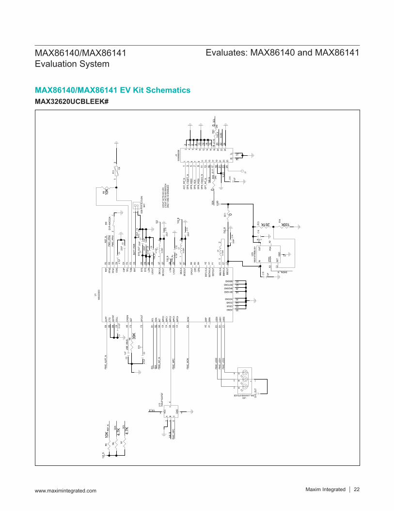
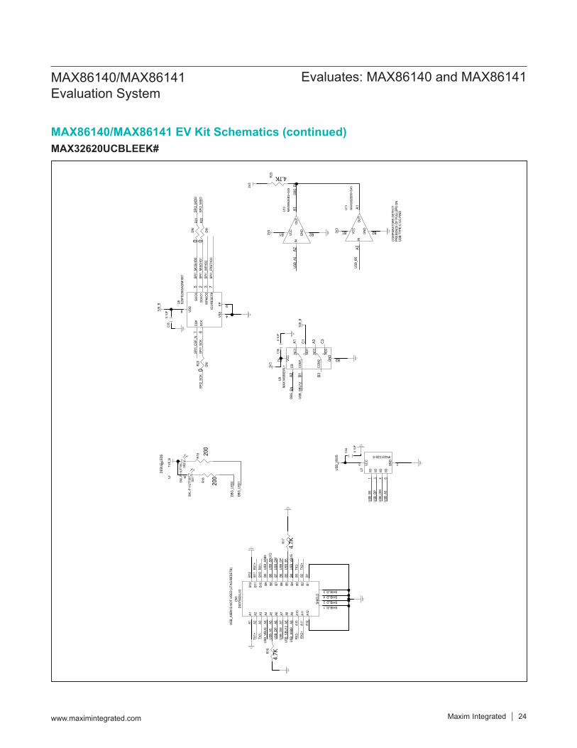
MAX86140/MAX86141 EV Kit SchematicsMAX32620UCBLEEK#
L2O
UT A
CTS
AS L
DO
ONL
Y O
NE IS
ENA
BLED
L1O
UT A
CTS
AS S
WIT
CH
DNI
22UF
B2B-
PH-K
-S(L
F)(S
N)
2.2U
H
DNI
10K
39K
00
0
261K
2.2U
H
22UF
22UF
1UF
0.1U
F
4.7U
F
10K
SML-LX0404SIUPGUSB
22UF
MAX
1819
EBL5
0+
1UF
22UF
5035
6625
00
22UF
22UF
10K 4.7K 4.7K
MAX
2030
3
1UF
4.7UF
4.7U
H
74AU
P1G
97G
F
EVP-
AWCD
2A
4.7U
F
4.7U
F4.7U
F
4.7U
F
100K
C14
C10
BAT
C6
U29
R30
R29
R6
U1
C3
C1C4
C8 C9 C12
C16
R5
R7
R8
R9
R14
R10
R11
C2
C15
C13
C7
C47
C5
R13
J3
C43
LED
U13
L1 L2
21
SW
L3
VLED
1V2
PMIC
_PFN
1
1V8_
B
1V8_
S
SPI0
_CSA
CC_N
SPI0
_SCK
ACC_
INT_
N
VLED
1V8_
S
J3.1
7SD
A
SPI0
_CSO
PT_N
SPI0
_MIS
O
SPI0
_MO
SI
OPT
_INT
_N
PMIC
_LED
2
PMIC
_LED
0PM
IC_L
ED1
J3.1
8SC
L
SCL
SYS_
OUT
PMIC
_MPC
BATT
_PW
R
1V8_
S
SDA
1V8_
S
SYS_
OUT
SHDNL_N
VLED
1V8_
B
1V8_
BPM
IC_M
PCRST_
N
SDA
1V8_
B
5V0_
B
3V3
USB_
VBUS
1V8_B
RST_
NPM
IC_P
FN2
PMIC
_ALR
T_N
SCL
PMIC
_INT
_N
PMIC
_MO
N
2511
C3G3
G4C4
B7
23
20
26
D6
10 24
191718
21
E5
E6
H3
D7
E7F7 C7
H6
H7 G7
A6
A7
G1
H2 F1E4
C6 H5
B4B5 B3
D5
C2A1A2
D3
A3
G2
G6
G5
B6 A5
E1 D1 C1E3C5
D2E2F6
B1 B2F3 F2A4 H4F5F4D4
12
A3
C3
A1C1 A2
C2
12
3 5 78
9
1213
1415
16 22
27
12
1
4
2
1 2
3 1 6
25
4
12
12
12
H1
64
3
27
26
2524
2322
2120
1918
1716
1514
1312
1110
98
76
54
32
1
BK1L
X
BK1GND
CHG
IN
SYS
BAT
BSTL
VLX
BSTH
VLX
BK1O
UT
L1IN
L1O
UTM
PC2
MPC
3
INT
BSTGND
BBLV
LX
RST
THM
TPU
SET
SFO
UT
BSTO
UT
BBHV
LX
ALRT
AGND
CAP
MO
N
PFN2
LED0
BBGND
QST
RTCT
G
VDIG
GSUB
PFN1
LED1
BBO
UT
CELL
MPC
0M
PC1
MPC
4
DGND
LED2
BK2O
UT
L2IN
CPO
UT
CPN
CPP
SDA
SCL
BK2L
X
BK2GND
L2O
UTSYS
HDGND
DRP
DRN
C
VCC
YA
GND
B
G
B
R
+
SHDN
SET
POK
OUT
IN
GND

Maxim Integrated │ 23www.maximintegrated.com
Evaluates: MAX86140 and MAX86141MAX86140/MAX86141 Evaluation System
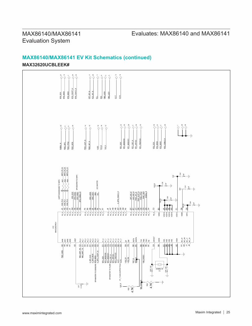
MAX86140/MAX86141 EV Kit Schematics (continued)MAX32620UCBLEEK#
D3/E
1/E2
ARE
NO
T US
ED IN
ORD
ER T
O K
EEP
GND
INTA
CT N
EAR
THE
BLE
ANTE
NNA
(NRF
5_UA
RT A
ND R
ESET
ARE
NO
T CO
NNEC
TED)
UART
/HAN
DSHA
KE T
O N
IMIT
Z
SPI S
LAVE
TO
NIM
ITZ
I2C
MAS
TER,
OR
SLAV
E TO
NIM
ITZ,
OR
TRI-S
TATE
SPI M
ASTE
R TO
SEN
SORS
OR
TRI-S
TATE
(IF >
5MM
)
(CO
MPO
NENT
S SO
LDER
DIR
ECTL
Y TO
TRA
CE)
NO S
TUBS
ON
PI F
ILTE
R
50O
HM T
L
MAX
1469
8 HA
S IN
TEG
RATE
D ES
D PR
OTE
CTIO
N
HAND
SHAK
E TO
NIM
ITZ33
DNI
0
DNI
DNI
1.8P
F1P
F
NRF5
2832
-CIA
A
12PF
12PF
33
100PF
0.1U
FM
AX14
689E
WL+
0.1U
F
0.1U
F
12PF
0.1U
FM
AX14
689E
WL+
MAX
1468
9EW
L+0.
1UF
33 33
1UF
32MHZ
0.1U
F
100PF
4.7UF
0
MAX
1468
9EW
L+
12PF
32.768KHZ
1PF
3.3N
H
12PF
2450AT18A100
DNI
0 0
0
0 0 00
DNI
DNI
R15
R34
R33
Z17
Z18
C19
U2
X2
U3U4
U5U6
C27
C22
C26
C30
C31
C32
C33
C25
C23
C24
C21
C28
A1
Y1RA
4RA
3
C20
RA2
RA1
C29
L4
Z44
R31
R32
R4R3R2R1
PMIC
_INT
_N
ACC_
INT_
NO
PT_I
NT_N
A_SP
I0_C
SACC
_NA_
SP0_
SCK
A_SP
I0_M
OSI
SPI0
_MO
SISP
I0_S
CKSP
I0_C
SACC
_N
SPI2
_SCK
SPI2
_CSB
LE_N
SPI0
_MIS
O
A_SP
I0_C
SOPT
_NSP
I0_C
SOPT
_N
SPI2
_MIS
OSP
I2_M
OSI
NRF5
_P0_
04
DBG
_LED
0
SPI1
_CSF
_N
NRF5
_SW
DCLK
RX1-
3V3
NRF5
_SW
DIO
DBG
_EN
NIM
_UAR
T_RX
TX1-
3V3
3V3
TX1+
3V3
NIM
_SW
DIO
NIM
_UAR
T_TX
DBG
_EN
RX2-
RX2+
TX2-
TX2+
NRF5
_UAR
T_TX
NIM
_SW
DCLK
DBG
_EN
NRF5
_UAR
T_RX
RX1+
DBG
_EN
1V8_
B
J3.1
8
SHDN
L_N
NRF5
_SW
DIO
NRF5
_SW
DCLK
PMIC
_MO
N
J3.1
7
SCL
NRF5
_P0_
03 SDA
PMIC
_MPC
PMIC
_PFN
2
DBG
_LED
1SP
I1_W
P/IO
2
NRF5
_UAR
T_RX
NRF5
_UAR
T_TX
SPI1
_FRS
T/IO
3NR
F5_P
0_31
PMIC
_ALR
T_N
D3F7 F6
2
21D
D2
H1
B2
A2
B6
A1G
7
D6F5E3C4C5
H7
B5A5A4A3B4B3E1F2G2
F3H2G3
H3H5G4
H6F4G6
E7E6C6D7 G5
C3
A6C2
B7
A2 B1 B3
B2
A1 A3C1 C3
C2
A2 B1 B3
B2
A1 A3C1 C3
C2
A2 B1 B3
B2
A1 A3C1 C3
C2
A2 B1 B3
B2
A1 A3C1 C3
C2
12
431
2
A7
G1F1
1
1
C7 H4 E2
VSS
VDD
P0.1
2
P0.1
4/TR
ACED
ATA3
P0.1
5/TR
ACED
ATA2
P0.1
6/TR
ACED
ATA1
P0.1
8/TR
ACED
ATA0
P0.2
1/NR
ESET
P0.0
8P0
.09
NFC2
/P0.
10
P0.1
3
P0.1
7
P0.2
0/TR
ACEC
LK
SWDI
O
P0.0
6P0
.07
VSS P0.1
1
P0.1
9
P0.2
2
SWDC
LK
P0.0
5/AI
N3P0
.04/
AIN2
VSS
P0.2
3P0
.24
P0.0
0/XL
1
P0.0
3/AI
N1
P0.2
6
VSS_PA
ANT
P0.0
1/XL
2P0
.02/
AIN0
VSS
NC
DEC3
DEC1
DCC
P0.3
1/AI
N7
P0.2
7
P0.2
5
XC1
VDD
DEC4
P0.3
0/AI
N6P0
.29/
AIN5
P0.2
8/AI
N4
DEC2
XC2
GNDVC
CCB
NC1
NO2
COM
2
NO1
COM
1
NC2
GNDVC
CCB
NC1
NO2
COM
2
NO1
COM
1
NC2
GNDVC
CCB
NC1
NO2
COM
2
NO1
COM
1
NC2
GNDVC
CCB
NC1
NO2
COM
2
NO1
COM
1
NC2
NC
INPUT
Maxim Integrated │ 24www.maximintegrated.com
Evaluates: MAX86140 and MAX86141MAX86140/MAX86141 Evaluation System
MAX86140/MAX86141 EV Kit Schematics (continued)MAX32620UCBLEEK#
DEBU
G L
EDS
USB_
A9B9
IS N
OT
USED
(JTA
G R
ESET
B)
USB
TYPE
-C C
C PI
NSPR
ESEN
CE O
F PU
LLUP
S O
NCO
MPA
RATO
RS D
ETEC
T
200
DNI
0DN
I
DNI
0
SML-
P11U
TT86
MAX
9062
EBS+
G45
0.1U
F
IP4221CZ6-S
MAX
9062
EBS+
G45
0.1U
F
4.7K
SML-
P11U
TT86
0.1U
F
200
DX07
S024
JJ3
S25F
S256
SAG
NFI0
01
4.7K
4.7K
MAX
1468
9EW
L+
0R1
8R2
0R2
1R2
2
DS1
CN1
U10 U1
1
DS2
U8
R17
C34
C36
C35
R23
R19
U7
R16
U9
USB_
A5
RX2+
TX1+
USB_
DM
DBG
_LED
1
DBG
_LED
0
SPI2
_SCK
SPI2
_MIS
OSP
I2_M
OSI
SPI1
_MIS
O/IO
1
USB_
B5US
B_DP
USB_
DM
USB_
SBU1
2
SPI1
_WP/
IO2
TX1-
USB_
A9B9
SPI1
_SCK
3V3
DBG
_EN
3V3
USB_
VBUS
RX1+
RX1-
USB_
SBU1
2
USB_
B5
1V8_
B
USB_
DP
1V8_
B
1V8_
B
SPI1
_CSF
_N
3V3
USB_
B5US
B_VB
USTX
2-
SPI1
_MO
SI/IO
0
USB_
A5
USB_
DMUS
B_DP
USB_
VBUS
USB_
A5
RX2-
USB_
SBU1
2US
B_A9
B9
TX2+
DBG
_EN
3V3
SPI1
_FRS
T/IO
3
C3A3C1A1
A3A2A1
9
A4 A5 A6 A7 A8 A9 A11
A12
B1B2B3B4B5B6B7B8B9B10
B11
B12
SHIELD_1SHIELD_2SHIELD_4SHIELD_3
B2
A2A1
B1 B2
A2A1
B1
A2 B1 B3
B2C2
AC
AC
1 65 2
8
2
1 3 4 6
5
3 7
4
A10
I/OI/OI/OI/OVC
C
GND
EP
VDD
WP#
/IO2
CS#
VSS
SO/IO
1
IO3/
RESE
T#
SCK
SI/IO
0
GNDVC
CCB
NC1
NO2
COM
2
NO1
COM
1
NC2
GNDVC
C
OUT
IN
GNDVC
C
OUT
IN
SHIE
LD
B12
B11
B10 B9 B8 B7 B6 B5 B4 B3 B2 B1
A12
A11
A10
A9A8A7A6A5A4A3A2A1
Maxim Integrated │ 25www.maximintegrated.com
Evaluates: MAX86140 and MAX86141MAX86140/MAX86141 Evaluation System
MAX86140/MAX86141 EV Kit Schematics (continued)MAX32620UCBLEEK#
SPI M
ASTE
R TO
NRF
5
SPI M
ASTE
R TO
SEN
SORS
P1_7
CAN
OUT
PUT
FCLK
UART
/HAN
DSHA
KE T
O N
RF5
SPI M
ASTE
R TO
FLA
SH
I2C
MAS
TER
0
MAX
3262
0IW
G+
4.7K
00
1UF
0.1U
F
1UF
1UF
1UF
12PF
1UF
4.7K
12PF
32.768KHZ
R24
R28
R27
U12
C37
R25
R26
C38
C39
C40
C41
C42
C46C4
5
Y2
22 6 8 20 14 10
27 15 247 23 17 325 11 9 5 13 1934 2 3528 33 32 29431 1 2616 18 12 3630
SPI2
_SCK
A_SP
I0_C
SACC
_N
SPI1
_MO
SI/IO
0
PMIC
_ALR
T_N
SPI2
_MO
SI
SPI2
_CSB
LE_N
SPI2
_MIS
O
NIM
_P2.
2NR
F5_P
0_31
SPI1
_MO
SI/IO
0SP
I1_S
CK
A_SP
I0_C
SOPT
_NSP
I0_M
ISO
1V8_
SSP
I1_M
ISO
/IO1
SPI1
_CSF
_N
PMIC
_ALR
T_N
DBG
_LED
0DB
G_L
ED1
SDA
SCL
OPT
_INT
_N
DBG
_LED
1
SPI0
_CSO
PT_N
SDA
ACC_
INT_
N
SPI0
_MO
SI
5V0_
B
J3.1
8
J3.1
7
SHDN
L_N
SPI1
_CSF
_N
SPI1
_FRS
T/IO
3
NRF5
_P0_
04
SPI2
_MO
SI
SPI2
_SCK
SPI0
_SCK
1V8_
B
1V2
SRST
_N
SPI1
_FRS
T/IO
3SP
I1_W
P/IO
2
J3.1
8J3
.17
PMIC
_MO
NNI
M_P
2.0
NRF5
_P0_
03
3V3
1V8_
B
A_SP
I0_M
OSI
A_SP
0_SC
K
NIM
_SW
DCLK
PMIC
_PFN
2PM
IC_M
PCSH
DNL_
N
OPT
_INT
_N
NIM
_UAR
T_RX
NIM
_UAR
T_TX
1V8_
B
RST_
N
USB_
DM
NIM
_SW
DIO
NIM
_P2.
1
PMIC
_INT
_N
PMIC
_MO
N
PMIC
_PFN
2
PMIC
_MPC
SPI0
_MIS
O
USB_
DP
PMIC
_INT
_N
DBG
_LED
0
VLED
SCL
SPI2
_MIS
O
SPI0
_CSA
CC_N
SPI1
_WP/
IO2
1V8_
B
SPI2
_CSB
LE_N
ACC_
INT_
N
SPI1
_SCK
SPI1
_MIS
O/IO
1
H7H3 J3 G4
F6
E4 F2 B9C9A4 A5 A6 A7 F8E8 A1 A9 J1 J9C2 C1 D4 D3 D1 D2 E3 E2 E1 F3 F4 E5 G2
G3
J2 H2 H4 G5
H5 F5 E6 H6 J6 G6
J7 F7 J8 H9 H8 G7
G9
G8
F9 D7 E7 C7 D6 C6 C5 D5 C4 C3
B2 B1 B4 B7B6B5
F1A8E9 H1J4B3 D8
A3
C8
B8 D9G1 J5 A2
12
VSS
VSS
VSS
VDD1
8
VDD1
8
VDD1
8VD
D18
NC_J
9NC
_J1
NC_A
9NC
_A1
DP DM VSS
P4_0
P4_2
P4_4
P4_6
VDDB
VRTC
32KO
UT
32KI
N
P4_1
P4_3
P4_5
P4_7
P5_0
P5_1
P5_2
P3_7
VDD1
2
P3_6
P5_3
P3_5
P5_4
P3_4
P3_3
P3_2
AIN3
P3_1
TDI
P3_0
AIN2
P2_7
TDO
P2_6
AIN1
TMS
AIN0
P2_5
VREF
P2_4
VSSA
P2_3
TCK
P2_2
P5_5
P2_1
VDDA
P2_0
P5_6
P1_7
P1_6
P1_4
P1_2
P1_0
P0_6
P0_4
P0_2
P0_0
SRST
N
P5_7
P1_5
P1_3
P1_1
P0_7
P0_5
P0_3
P0_1
RSTN
P6_0
Maxim Integrated │ 26www.maximintegrated.com
Evaluates: MAX86140 and MAX86141MAX86140/MAX86141 Evaluation System
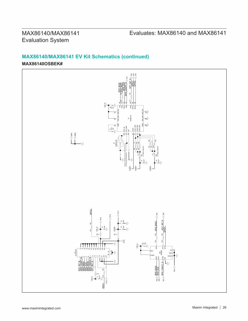
MAX86140/MAX86141 EV Kit Schematics (continued)MAX86140OSBEK#
TO T
HE C
ONN
ECTO
R G
ROUN
DG
ROUN
D LI
NE S
HOUL
D BE
RO
UTED
SEP
ARAT
ELY
VLED
+
VLED
+
VLED
+
LT P
4SG
-V1A
B-36
-F
BMA2
80
0DNI
VLED
+
0
1UF
0
100
LT P
4SG
-V1A
B-36
-F
DNI
1V8_
O
1V8_
ADN
I DNI
1UF
0
5016
1625
75
22UF
22UF
22UF
100
10V
100
1V8_
O
0
100
22UF
MAX
8614
0
100
100
10V
10V
10UF
22UF
1V8_
A
22UF
VEM
D551
0C
U2
TP9
TP12
TP2
R13
TP11
C2
R4
TP1
GND
2
GND
1
DS1
R7R6
U1
C4
TP10
DS2
C8
J1
R3
TP7
TP6
TP5
TP8
R8
R9
TP3
C6C5
C3
R15
R2
R14
C1
R11
R5
C9
R12
R10
R1
TP4
TP14
TP15
TP16
D1
C7
SPI0
_MO
SISP
I0_S
CK
SPI0
_CSA
CC_N
ACC_
INT_
N
OPT
_INT
_NSP
I0_C
SACC
_NSP
I0_M
OSI
SPI0
_SCK
GPI
O1
GPI
O1
J1_P
IN25
GPI
O2
GPI
O1
OPT
_INT
_N
GPI
O2
SPI0
_CSO
PT_N
SPI0
_SCK
SPI0
_MIS
OSP
I0_M
OSI
SPI0
_MIS
O
SPI0
_MIS
O
1V8_
ACCE
L
1V8_
OPT
ICAL
SPI0
_CSO
PT_N
ACC_
INT_
N
J1_V
LED
21
C4
C3
5
B3 B4
C5
1
3
4
9
11
12
B1C1D5 D1
D3
A1
12 10
A3 A5A2
6
A4 B2
8
2
7
C2
D2
B5
D4
12 3
4
SCX
PSCSB
GND
GNDIO
VDD
INT2
INT1
NC
VDDIO
SDX
SDO
VLED
NC
VREF
SCLKSD
I
PGND
VDD_
ANA
LED1
_DRV
PD1_
IN
GND
_ANA
GND
_DIG
VDD_
DIG
LED2
_DRV
PD_G
ND
GPI
O2
GPI
O1
INTB
LED3
_DRV
SDO
CSB
27
26
2524
2322
2120
1918
1716
1514
1312
1110
98
76
54
32
1
Maxim Integrated │ 27www.maximintegrated.com
Evaluates: MAX86140 and MAX86141MAX86140/MAX86141 Evaluation System
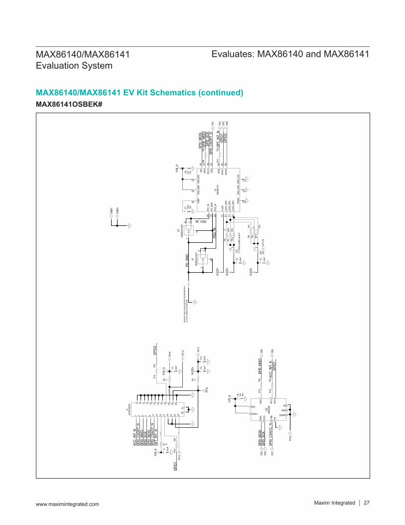
MAX86140/MAX86141 EV Kit Schematics (continued)MAX86141OSBEK#
TO T
HE C
ONN
ECTO
R G
ROUN
DG
ROUN
D LI
NE S
HOUL
D BE
RO
UTED
SEP
ARAT
ELY
VLED
+
VLED
+
22UF
VEM
D501
0X01
1V8_
O
10V
LED_
LY_P
47F-
TM
VEM
D501
0X01
MAX
8614
1
LT P
WSG
-AAB
B-36
-46-
F
10UF
VLED
+
DNI
DNI DN
I
1V8_
A
DNI
22UF
5016
1625
75
22UF
22UF
0
100
1V8_
O0
10V
10V
0
BMA2
8010
0
100
1UF
0
22UF
100
100
1UF
1V8_
A
0VL
ED+
22UF
100
C8
C4
DS2
D2
C7
D1
DS1
R6
C5
R4
J1
R14
C3C1
0
C1
R15
TP11
TP8
TP4
TP3
TP5
R2
R11
TP10
R9
U2
R13
R7
R5
TP12
TP6
TP7
R12
TP9
R8
R10
GND
1
GND
2
R1
U1
TP2
TP1
C9
C2TP
14
TP15
R3
TP16
PD_G
ND
PD1_IN
SPI0
_MIS
OSP
I0_S
CKSP
I0_C
SOPT
_N
ACC_
INT_
NG
PIO
1
PD2_
IN
OPT
_INT
_N
SPI0
_MIS
O
J1_P
IN25
J1_V
LED
1V8_
OPT
ICAL
1V8_
ACCE
L
SPI0
_CSA
CC_N
SPI0
_MO
SISP
I0_S
CK
SPI0
_CSO
PT_N
ACC_
INT_
N
GPI
O2
GPI
O1
GPI
O2
GPI
O1
SPI0
_CSA
CC_N
OPT
_INT
_N
SPI0
_MO
SI
SPI0
_SCK
SPI0
_MO
SISP
I0_M
ISO
21
21
4
321
4
321
A2 A5 B3A3D5 C5 D4
B5
C3
D3
C4
B4
7
2
8
4
9
11
5
B1
6
D2
A1
12 10
1
3
C1D1
B2
C2
A4
SCX
PSCSB
GND
GNDIO
VDD
INT2
INT1
NC
VDDIO
SDX
SDO
VLED
SCLK
VREF
PD2_
IN
SDI
PGND
VDD_
ANA
LED1
_DRV
PD1_
IN
GND
_ANA
GND
_DIG
VDD_
DIG
LED2
_DRV
PD_G
ND
GPI
O2
GPI
O1
INTB
LED3
_DRV
SDO
CSB
27
26
2524
2322
2120
1918
1716
1514
1312
1110
98
76
54
32
1
Maxim Integrated │ 28www.maximintegrated.com
Evaluates: MAX86140 and MAX86141MAX86140/MAX86141 Evaluation System
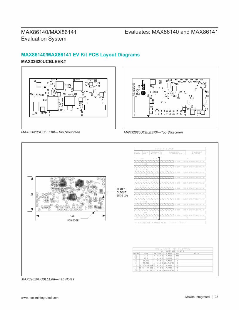
MAX32620UCBLEEK#—Top Silkscreen MAX32620UCBLEEK#—Top Silkscreen
MAX32620UCBLEEK#—Fab Notes
MAX86140/MAX86141 EV Kit PCB Layout DiagramsMAX32620UCBLEEK#
.69
PLATEDCUTOUT EDGE (2X)
1.38
PCB EDGE
Maxim Integrated │ 29www.maximintegrated.com
Evaluates: MAX86140 and MAX86141MAX86140/MAX86141 Evaluation System
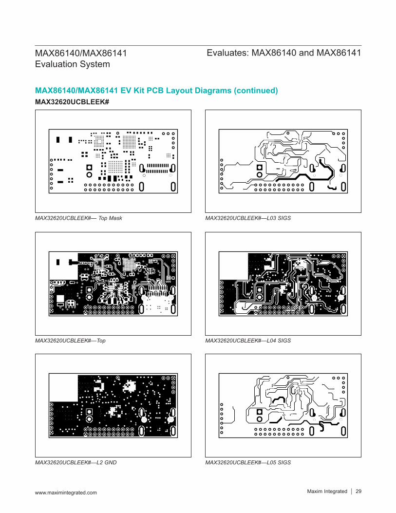
MAX32620UCBLEEK#— Top Mask MAX32620UCBLEEK#—L03 SIGS
MAX32620UCBLEEK#—Top MAX32620UCBLEEK#—L04 SIGS
MAX32620UCBLEEK#—L2 GND MAX32620UCBLEEK#—L05 SIGS
MAX86140/MAX86141 EV Kit PCB Layout Diagrams (continued)MAX32620UCBLEEK#
Maxim Integrated │ 30www.maximintegrated.com
Evaluates: MAX86140 and MAX86141MAX86140/MAX86141 Evaluation System
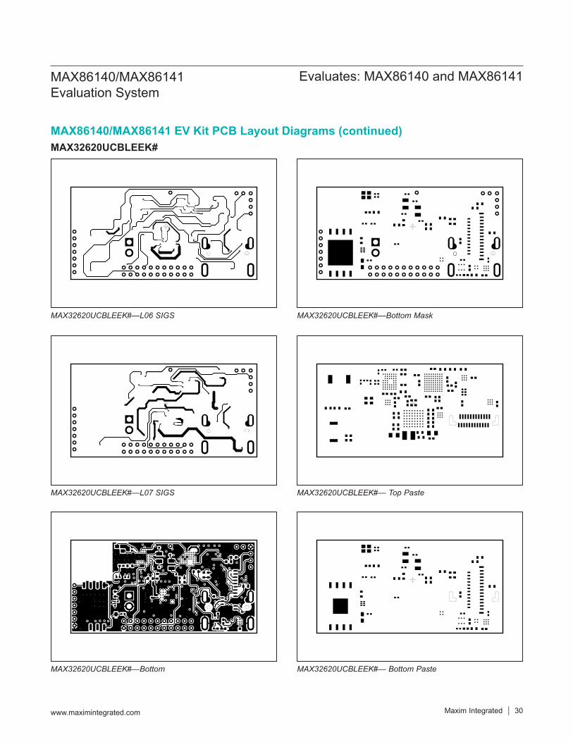
MAX32620UCBLEEK#—L06 SIGS MAX32620UCBLEEK#—Bottom Mask
MAX32620UCBLEEK#—L07 SIGS MAX32620UCBLEEK#— Top Paste
MAX32620UCBLEEK#—Bottom MAX32620UCBLEEK#— Bottom Paste
MAX86140/MAX86141 EV Kit PCB Layout Diagrams (continued)MAX32620UCBLEEK#
Maxim Integrated │ 31www.maximintegrated.com
Evaluates: MAX86140 and MAX86141MAX86140/MAX86141 Evaluation System
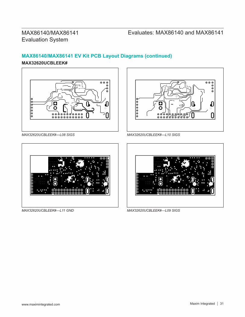
MAX32620UCBLEEK#—L08 SIGS MAX32620UCBLEEK#—L10 SIGS
MAX32620UCBLEEK#—L11 GND MAX32620UCBLEEK#—L09 SIGS
MAX86140/MAX86141 EV Kit PCB Layout Diagrams (continued)MAX32620UCBLEEK#

Maxim Integrated │ 32www.maximintegrated.com
Evaluates: MAX86140 and MAX86141MAX86140/MAX86141 Evaluation System
MAX86140OSBEK#—Fab Notes
MAX86140/MAX86141 EV Kit PCB Layout Diagrams (continued)MAX86140OSBEK#
1”
.472
.735
BOTTOM SIDE REQUIRES BLACK SOLDERMASK
Maxim Integrated │ 33www.maximintegrated.com
Evaluates: MAX86140 and MAX86141MAX86140/MAX86141 Evaluation System
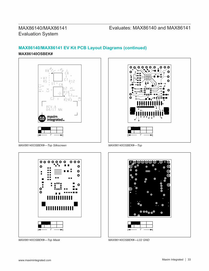
MAX86140OSBEK#—Top Silkscreen MAX86140OSBEK#—Top
MAX86140OSBEK#—Top Mask MAX86140OSBEK#—L02 GND
MAX86140/MAX86141 EV Kit PCB Layout Diagrams (continued)MAX86140OSBEK#
1” 1”
1” 1”
Maxim Integrated │ 34www.maximintegrated.com
Evaluates: MAX86140 and MAX86141MAX86140/MAX86141 Evaluation System
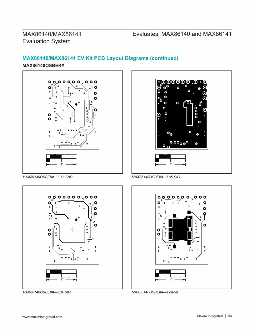
MAX86140OSBEK#—L03 GND MAX86140OSBEK#—L05 SIG
MAX86140OSBEK#—L04 SIG MAX86140OSBEK#—Bottom
MAX86140/MAX86141 EV Kit PCB Layout Diagrams (continued)MAX86140OSBEK#
1” 1”
1” 1”
Maxim Integrated │ 35www.maximintegrated.com
Evaluates: MAX86140 and MAX86141MAX86140/MAX86141 Evaluation System
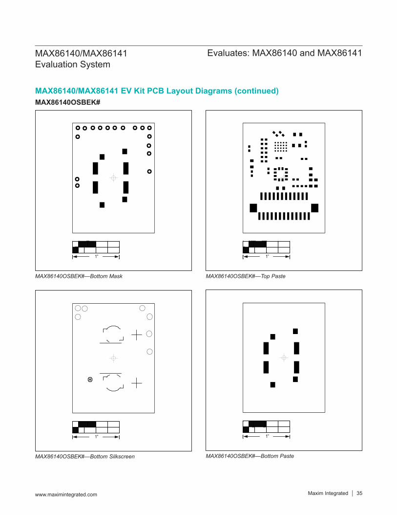
MAX86140OSBEK#—Bottom Mask
MAX86140OSBEK#—Bottom Silkscreen
MAX86140OSBEK#—Top Paste
MAX86140OSBEK#—Bottom Paste
MAX86140/MAX86141 EV Kit PCB Layout Diagrams (continued)MAX86140OSBEK#
1”
1”
1”
1”
Maxim Integrated │ 36www.maximintegrated.com
Evaluates: MAX86140 and MAX86141MAX86140/MAX86141 Evaluation System
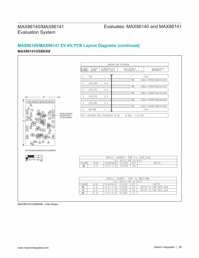
MAX86141OSBEK#—Fab Notes
MAX86140/MAX86141 EV Kit PCB Layout Diagrams (continued)MAX86141OSBEK#
1”
.472
.735
BOTTOM SIDE REQUIRES BLACK SOLDERMASK
WE ARE ACCEPTEDDUPLICATE DRILLAT THIS LOCATION
Maxim Integrated │ 37www.maximintegrated.com
Evaluates: MAX86140 and MAX86141MAX86140/MAX86141 Evaluation System
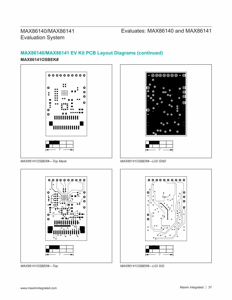
MAX86141OSBEK#—Top Mask MAX86141OSBEK#—L02 GND
MAX86141OSBEK#—Top MAX86141OSBEK#—L03 SIG
MAX86140/MAX86141 EV Kit PCB Layout Diagrams (continued)MAX86141OSBEK#
1” 1”
1” 1”
Maxim Integrated │ 38www.maximintegrated.com
Evaluates: MAX86140 and MAX86141MAX86140/MAX86141 Evaluation System
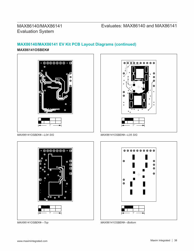
MAX86141OSBEK#—L04 SIG MAX86141OSBEK#—L05 SIG
MAX86141OSBEK#—Top MAX86141OSBEK#—Bottom
MAX86140/MAX86141 EV Kit PCB Layout Diagrams (continued)MAX86141OSBEK#
1” 1”
1” 1”
Maxim Integrated │ 39www.maximintegrated.com
Evaluates: MAX86140 and MAX86141MAX86140/MAX86141 Evaluation System
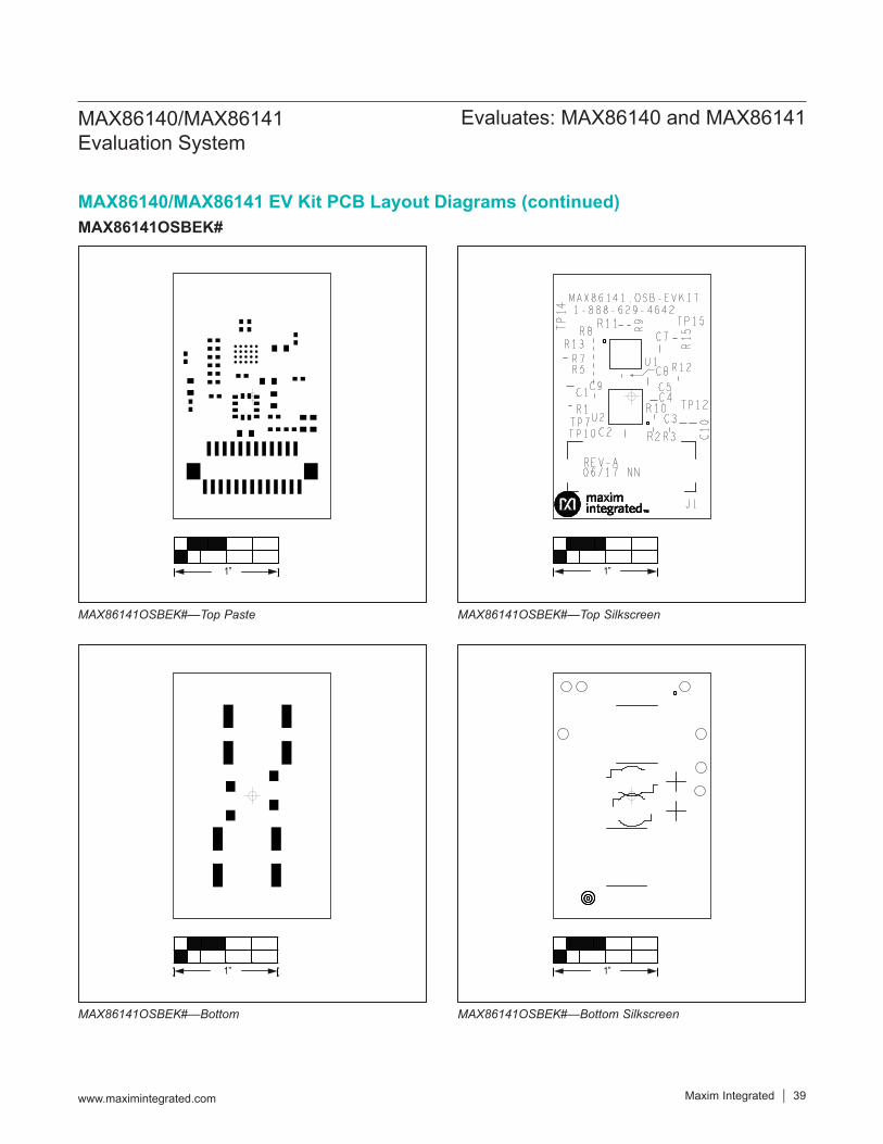
MAX86141OSBEK#—Top Paste MAX86141OSBEK#—Top Silkscreen
MAX86141OSBEK#—Bottom MAX86141OSBEK#—Bottom Silkscreen
MAX86140/MAX86141 EV Kit PCB Layout Diagrams (continued)MAX86141OSBEK#
1” 1”
1” 1”

Maxim Integrated cannot assume responsibility for use of any circuitry other than circuitry entirely embodied in a Maxim Integrated product. No circuit patent licenses are implied. Maxim Integrated reserves the right to change the circuitry and specifications without notice at any time.
Maxim Integrated and the Maxim Integrated logo are trademarks of Maxim Integrated Products, Inc. © 2017 Maxim Integrated Products, Inc. │ 40
Evaluates: MAX86140 and MAX86141MAX86140/MAX86141 Evaluation System
Revision HistoryREVISIONNUMBER
REVISIONDATE DESCRIPTION PAGES
CHANGED
0 8/17 Initial release —
For pricing, delivery, and ordering information, please contact Maxim Direct at 1-888-629-4642, or visit Maxim Integrated’s website at www.maximintegrated.com.