may 2003 rev. 1.0
TRANSCRIPT

xr XRT73L02MTWO CHANNEL E3/DS3/STS-1 LINE INTERFACE UNIT
MAY 2003 REV. 1.0.0
GENERAL DESCRIPTIONThe XRT73L02M is a two-channel fully integratedLine Interface Unit (LIU) for E3/DS3/STS-1 applica-tions. It incorporates independent Receivers, Trans-mitters in a single 100 pin TQFP package.
The XRT73L02M can be configured to operate in ei-ther E3 (34.368 MHz), DS3 (44.736 MHz) or STS-1(51.84 MHz) modes.The transmitter can be turned offor tri-stated for redundancy support and for conserv-ing power.
The XRT73L02M’s differential receiver provides highnoise interference margin and is able to receive thedata over 1000 feet of cable or with up to 12 dB of ca-ble attenuation.
The XRT73L02M provides both Serial Microproces-sor Interface as well as Hardware mode for program-ming and control.
The XRT73L02M supports local,remote and digitalloop-backs. The XRT73L02M also contains an on-board Pseudo Random Binary Sequence (PRBS)generator and detector with the ability to insert anddetect single bit error.
FEATURESRECEIVER:
• On chip Clock and Data Recovery circuit for highinput jitter tolerance.
• Meets the jitter tolerance requirements as specifiedin ITU-T G.823_1993 for E3 and Telcordia GR-499-CORE for DS3 applications.
• Detects and Clears LOS as per G.775.
• Receiver Monitor mode handles up to 20 dB flatloss with 6 dB cable attenuation.
• On chip B3ZS/HDB3 encoder and decoder that caneither be enabled or disabled.
• On-chip clock synthesizer generates the appropri-ate rate clock from a single frequency XTAL.
• Provides low jitter clock outputs for either DS3,E3or STS-1 rates.
• On-chip clock synthesizer provides the appropriaterate clock from a single 12.288 MHz Clock.
• Provides low jitter output clock.
TRANSMITTER:
• Compliant with Bellcore GR-499, GR-253 and ANSIT1.102 Specification for transmit pulse
• Tri-state Transmit output capability for redundancyapplications
• Transmitter can be turned on or off.
CONTROL AND DIAGNOSTICS:
• 5 wire Serial Microprocessor Interface for controland configuration.
• Supports optional internal Transmit Driver Monitor-ing.
• PRBS error counter register to accumulate errors.
• Hardware Mode for control and configuration.
• Supports Local, Remote and Digital Loop-backs.
• Single 3.3 V ± 5% power supply.
• 5 V Tolerant I/O.
• Available in 100 pin TQFP.
• -40°C to 85°C Industrial Temperature Range.
APPLICATIONS• E3/DS3 Access Equipment.
• STS1-SPE to DS3 Mapper.
• DSLAMs.
• Digital Cross Connect Systems.
• CSU/DSU Equipment.
• Routers.
• Fiber Optic Terminals.
Exar Corporation 48720 Kato Road, Fremont CA, 94538 • (510) 668-7000 • FAX (510) 668-7017 • www.exar.com

XRT73L02M xr
TWO CHANNEL E3/DS3/STS-1 LINE INTERFACE UNIT
TRANSMIT INTERFACE CHARACTERISTICS
• Accepts either Single-Rail or Dual-Rail data fromTerminal Equipment and generates a bipolar signalto the line
• Integrated Pulse Shaping Circuit.
• Built-in B3ZS/HDB3 Encoder (which can be dis-abled).
• Accepts Transmit Clock with duty cycle of 30%-70%.
• Generates pulses that comply with the ITU-T G.703pulse template for E3 applications.
• Generates pulses that comply with the DSX-3 pulsetemplate, as specified in Bellcore GR-499-COREand ANSI T1.102_1993.
• Generates pulses that comply with the STSX-1pulse template, as specified in Bellcore GR-253-CORE.
• Transmitter can be turned off in order to supportredundancy designs.
RECEIVE INTERFACE CHARACTERISTICS
• Integrated Adaptive Receive Equalization for opti-mal Clock and Data Recovery.
• Declares and Clears the LOS defect per ITU-TG.775 requirements for E3 and DS3 applications.
• Meets Jitter Tolerance Requirements, as specifiedin ITU-T G.823_1993 for E3 Applications.
• Meets Jitter Tolerance Requirements, as specifiedin Bellcore GR-499-CORE for DS3 Applications.
• Declares Loss of Signal (LOS) and Loss of Lock(LOL) Alarms.
• Built-in B3ZS/HDB3 Decoder (which can be dis-abled).
• Recovered Data can be muted while the LOS Con-dition is declared.
• Outputs either Single-Rail or Dual-Rail data to theTerminal Equipment.
FIGURE 1. BLOCK DIAGRAM OF THE XRT 73L02M
HOST/HWSTS-1/DS3
E3REQEN
RTIPRRING
SR/DR
XRT75L03
RLBRLOS
TPOSTNEGTxClkTAOSTxLEVTxON
Note: Serial Processor Interface input pins are shared by in "Host" Mode and redefined in the "Hardware" Mode.
DeviceMonitor
MTIPMRING
DMO
TimingControl
TTIP
TRINGTx
PulseShaping
HDB3/B3ZS
Encoder
RLOLRxONRxClkINV
RxClk
RPOSRNEG/LCV
TxControl
MUXLine
Driver
LLB
Invert
RemoteLoopBack
HDB3/B3ZS
DecoderMUXAGC/
Equalizer
Peak Detector
LOSDetector
Slicer
SerialProcessorInterface
LocalLoopBack
Clock & DataRecovery
ClockSynthesizer
E3Clk,DS3Clk,STS-1Clk
RESETCS
SClkINT
SDOSDI CLK_OUT
2

xr XRT73L02M
TWO CHANNEL E3/DS3/STS-1 LINE INTERFACE UNIT REV. 1.0.0
FIGURE 2. PIN OUT OF THE XRT73L02M
XRT73L02M
1 2 3 4 5 6 7 8 9 10 11 12 13 14 15 16 17 18 19 20 21 22 23 24 25
75 74 73 72 71 70 69 68 67 66 65 64 63 62 61 60 59 58 57 56 55 54 53 52 51
50494847464544434241403938373635343332313029282726
767778798081828384858687888990919293949596979899100
TAO
S_0
TxLE
V_0
MR
ING
_0M
TIP_
0TR
ING
_0TT
IP_0
TxD
VDD
_0Tx
DG
ND
_0D
VDD
E3C
LKD
GN
DD
GN
DD
S3C
LKD
VDD
DVD
DST
S1C
LK/S
FMC
LKD
GN
DTx
DG
ND
_1Tx
DVD
D_1
TTIP
_1TR
ING
_1M
TIP_
1M
RIN
G_1
TxLE
V_1
TAO
S_1
REQ
EN_0
E3_0
STS1
/DS3
_0LL
B_0
RLB
_0R
xAVD
D_0
RxA
GN
D_0
RR
ING
_0R
TIP_
0AG
ND
RxA
RxB
AVD
DAG
ND
AGN
DAG
ND
RTI
P_1
RR
ING
_1R
xAG
ND
_1R
xAVD
D_1
RLB
_1LL
B_1
STS1
/DS3
_1E3
_1R
EQEN
_1
TNEG_1TPOS_1TxCLK_1DMO_1CLKOUT_1CLKOUT_ENTxAGND_1TxAVDD_1AGND_1AVDD_1DVDD_1DGND_1DVDD_1DGND_1RxCLK_1RPOS_1RNEG/LCV_1RLOS_1RLOL_1SDI/RxONSCLK/TxCLKINVCS/RxCLKINVINT/LOSMUTSDO/RxMONHOST/HW
TNEG_0TPOS_0
TxCLK_0DMO_0
CLKOUT_0TxON
TxMONTxAGND_0TxAVDD_0
AGND_0AVDD_0DVDD_0DGND_0
RxDVDD_0RxDGND_0
RxCLK_0RPOS_0
RNEG/LCV_0RLOS_0RLOL_0
TESTRESET
ICTSFM_EN
SR/DR
ORDERING INFORMATIONPART NUMBER PACKAGE OPERATING TEMPERATURE RANGE
XRT73L02MIV 14mm x 14mm 100 Pin TQFP -40°C to +85°C
3

XRT73L02M xrTWO CHANNEL E3/DS3/STS-1 LINE INTERFACE UNIT
REV. 1.0.0
TABLE OF CONTENTS
GENERAL DESCRIPTION ............................................................................................... 1FEATURES .................................................................................................................................................... 1APPLICATIONS .............................................................................................................................................. 1
Figure 1. Block Diagram of the XRT73L02M ..................................................................................................... 2TRANSMIT INTERFACE CHARACTERISTICS ...................................................................................................... 2RECEIVE INTERFACE CHARACTERISTICS ........................................................................................................ 2
Figure 2. Pin Out of the XRT73L02M ................................................................................................................ 3ORDERING INFORMATION ................................................................................................................... 3
TABLE OF CONTENTS .................................................................................................................................... I PIN DESCRIPTIONS (BY FUNCTION) ............................................................................ 4
TRANSMIT INTERFACE ................................................................................................................................... 4RECEIVE INTERFACE ..................................................................................................................................... 6CLOCK INTERFACE ........................................................................................................................................ 9OPERATING MODE SELECT ......................................................................................................................... 10CONTROL AND ALARM INTERFACE ............................................................................................................... 14ANALOG POWER AND GROUND ................................................................................................................... 15DIGITAL POWER AND GROUND ..................................................................................................................... 161.0 ELECTRICAL CHARACTERISTICS ................................................................................................. 17
TABLE 1: ABSOLUTE MAXIMUM RATINGS ............................................................................................................ 17TABLE 2: DC ELECTRICAL CHARACTERISTICS: ................................................................................................... 17
2.0 TIMING CHARACTERISTICS ............................................................................................................ 18Figure 3. Typical interface between terminal equipment and the XRT73L02M (dual-rail data) ...................... 18Figure 4. Transmitter Terminal Input Timing ................................................................................................... 18Figure 5. Receiver Data output and code violation timing .............................................................................. 19Figure 6. Transmit Pulse Amplitude test circuit for E3, DS3 and STS-1 Rates ............................................... 20
3.0 LINE SIDE CHARACTERISTICS: ..................................................................................................... 203.1 E3 LINE SIDE PARAMETERS: ............................................................................................................................. 20
Figure 7. Pulse Mask for E3 (34.368 mbits/s) interface as per itu-t G.703 ..................................................... 20TABLE 3: E3 TRANSMITTER LINE SIDE OUTPUT AND RECEIVER LINE SIDE INPUT SPECIFICATIONS ........................... 21Figure 8. Bellcore GR-253 CORE Transmit Output Pulse Template for SONET STS-1 Applications ............ 22TABLE 4: STS-1 PULSE MASK EQUATIONS ........................................................................................................ 22TABLE 5: STS-1 TRANSMITTER LINE SIDE OUTPUT AND RECEIVER LINE SIDE INPUT SPECIFICATIONS (GR-253) . 23Figure 9. Transmit Ouput Pulse Template for DS3 as per Bellcore GR-499 .................................................. 23TABLE 6: DS3 PULSE MASK EQUATIONS ........................................................................................................... 24TABLE 7: DS3 TRANSMITTER LINE SIDE OUTPUT AND RECEIVER LINE SIDE INPUT SPECIFICATIONS (GR-499) ..... 24Figure 10. Microprocessor Serial Interface Structure ...................................................................................... 25Figure 11. Timing Diagram for the Microprocessor Serial Interface ................................................................ 25TABLE 8: MICROPROCESSOR SERIAL INTERFACE TIMINGS ( TA = 250C, VDD=3.3V± 5% AND LOAD = 10PF) ..... 26FUNCTIONAL DESCRIPTION: ........................................................................................ 27
4.0 The Transmitter Section: ................................................................................................................. 27Figure 12. Single-Rail or NRZ Data Format (Encoder and Decoder are Enabled) ......................................... 27Figure 13. Dual-Rail Data Format (encoder and decoder are disabled) ......................................................... 27
4.0.1 Transmit Clock: .................................................................................................................................. 284.0.2 B3ZS/HDB3 Encoder: ......................................................................................................................... 28
Figure 14. B3ZS Encoding Format ................................................................................................................. 284.0.3 Transmit Pulse Shaper: ..................................................................................................................... 29
Figure 15. HDB3 Encoding Format ................................................................................................................. 294.0.4 Transmit Drive Monitor: ..................................................................................................................... 304.0.5 Transmitter Section On/Off: .............................................................................................................. 30
Figure 16. Transmit Driver Monitor set-up. ..................................................................................................... 305.0 The Receiver Section: ...................................................................................................................... 31
5.0.1 AGC/Equalizer: ................................................................................................................................... 31
IV

xr XRT73L02MTWO CHANNEL E3/DS3/STS-1 LINE INTERFACE UNIT
REV. 1.0.0
Figure 17. Interference Margin Test Set up for DS3/STS-1 ........................................................................... 32Figure 18. Interference Margin Test Set up for E3. ........................................................................................ 32TABLE 9: INTERFERENCE MARGIN TEST RESULTS .............................................................................................. 32
5.0.2 Clock and Data Recovery: ................................................................................................................. 335.0.3 B3ZS/HDB3 Decoder: ........................................................................................................................ 335.0.4 LOS (Loss of Signal) Detector: ......................................................................................................... 34
DISABLING ALOS/DLOS DETECTION: ......................................................................................................... 34TABLE 10: THE ALOS (ANALOG LOS) DECLARATION AND CLEARANCE THRESHOLDS FOR A GIVEN SETTING OF
LOSTHR AND REQEN (DS3 AND STS-1 APPLICATIONS) ................................................................... 34Figure 19. Loss Of Signal Definition for E3 as per ITU-T G.775 .................................................................... 35Figure 20. Loss of Signal Definition for E3 as per ITU-T G.775. .................................................................... 35
6.0 Jitter: ................................................................................................................................................. 366.0.1 Jitter Tolerance - Receiver: ............................................................................................................... 36
Figure 21. Jitter Tolerance Measurements ..................................................................................................... 36Figure 22. Input Jitter Tolerance For DS3/STS-1 .......................................................................................... 37Figure 23. Input Jitter Tolerance for E3 ......................................................................................................... 37
6.0.2 Jitter Transfer - Receiver/Transmitter: ............................................................................................. 38TABLE 11: JITTER AMPLITUDE VERSUS MODULATION FREQUENCY (JITTER TOLERANCE) ..................................... 38TABLE 12: JITTER TRANSFER SPECIFICATION/REFERENCES ............................................................................... 38TABLE 13: JITTER TRANSFER PASS MASKS ....................................................................................................... 39Figure 24. Jitter Transfer Requirements and Jitter Attenuator Performance .................................................. 39
6.1.1 Jitter Generation: ............................................................................................................................... 407.0 Serial Host interface: ....................................................................................................................... 40
TABLE 14: FUNCTIONS OF SHARED PINS ............................................................................................................ 40TABLE 15: REGISTER MAP AND BIT NAMES ....................................................................................................... 40TABLE 16: REGISTER MAP DESCRIPTION - GLOBAL ............................................................................................ 41TABLE 17: REGISTER MAP AND BIT NAMES - CHANNEL 0 REGISTERS ................................................................. 42TABLE 18: REGISTER MAP AND BIT NAMES - CHANNEL 1 REGISTERS ................................................................. 42TABLE 20: REGISTER MAP DESCRIPTION ........................................................................................................... 43
8.0 Diagnostic Features: ........................................................................................................................ 478.1 PRBS GENERATOR AND DETECTOR: ................................................................................................................ 478.2 LOOPBACKS: ............................................................................................................................................... 48
8.2.1 ANALOG LOOPBACK: ....................................................................................................................... 48Figure 25. PRBS MODE ................................................................................................................................. 48
8.2.2 DIGITAL LOOPBACK: ........................................................................................................................ 49Figure 26. Analog Loopback ........................................................................................................................... 49
8.2.3 REMOTE LOOPBACK: ....................................................................................................................... 50Figure 27. Digital Loopback ............................................................................................................................ 50
8.3 TRANSMIT ALL ONES (TAOS): ................................................................................................................... 51Figure 28. Remote Loopback ......................................................................................................................... 51Figure 29. Transmit All Ones (TAOS) ............................................................................................................. 51APPENDIX ......................................................................................................................... 52Figure 30. EVALUATION BOARD SCHEMATICS ......................................................................................... 52Figure 31. Evaluation Board Schematics ....................................................................................................... 53
ORDERING INFORMATION ................................................................................................................ 54PACKAGE DIMENSIONS - 14X20 MM, 100PIN PACKAGE ................................................................................ 54REVISIONS ................................................................................................................................................. 55
V

XRT73L02M xrTWO CHANNEL E3/DS3/STS-1 LINE INTERFACE UNIT REV. 1.0.0
PIN DESCRIPTIONS (BY FUNCTION)
TRANSMIT INTERFACE
PIN # SIGNAL NAME TYPE DESCRIPTION
81 TxON I Transmitter ON Input :
This pin is active only when the corresponding TxON bit is set.
Table below shows the status of the transmitter based on theTxON bit and TxONpin settings.
NOTES: 1. This pin will be active and can control the TTIP and TRING outputs only
when the TxON_n bits in the channel register are set .
2. When Transmitters are turned off the TTIP and TRING outputs are Tri-stated.
3. This pin is internally pulled up.
78
48
TxCLK_0
TxCLK_1
I Transmit Clock Input for TPOS and TNEG - Channel 0:
Transmit Clock Input for TPOS and TNEG - Channel 1:
The frequency accuracy of this input clock must be of nominal bit rate ± 20 ppm.The duty cycle can be 30%-70%.
By default, input data is sampled on the falling edge of TxCLK when input datais changing on the rising edge of TxCLK..
76
50
TNEG_0
TNEG_1
I Transmit Negative Data Input - Channel 0:
Transmit Negative Data Input - Channel 1:
In Dual-rail mode, these pins are sampled on the falling or rising edge ofTxCLK_n
NOTE: These input pins are ignored and must be grounded if the Transmitter Section is configured to accept Single-Rail data from the Terminal Equipment.
77
49
TPOS_0
TPOS_1
I Transmit Positive Data Input - Channel 0:
Transmit Positive Data Input - Channel 1:
By default sampled on the falling edge of TxCLK
70
56
TTIP_0
TTIP_1
O Transmit TTIP Output - Channel 0:
Transmit TTIP Output - Channel 1:
These pins along with TRING transmit bipolar signals to the line using a 1:1transformer.
71
55
TRING_0
TRING_1
O Transmit Ring Output - Channel 0:
Transmit Ring Output - Channel 1:
These pins along with TTIP transmit bipolar signals to the line using a 1:1 trans-former.
Bit
0
0
Transmitter Status
OFF
OFF
Pin
0
1
1
1
OFF
ON
0
1
4

xr XRT73L02MTWO CHANNEL E3/DS3/STS-1 LINE INTERFACE UNIT
REV. 1.0.0
30 TxClkINV/
SClk
I Hardware Mode: Transmit Clock Invert
Host Mode: Serial Clock Input:
Function of this pin depends on whether the XRT73L02M is configured to oper-ate in Hardware mode or Host mode.
In Hardware mode, setting this input pin “High” configures all the Transmitters tosample the TPOS_n and TNEG_n data on the rising edge of the TxClk_n .
NOTES: 1. If the XRT73L02M is configured in HOST mode, this pin functions as
SClk input pin (please refer to the pin description for Microprocessor interface).
82 TxMON I Transmitter Monitor:
When this pin is pulled “High”, MTIP and MRING are connected internally toTTIP and TRING and allows self monitoring of the transmitter.
74
52
TxLEV_0
TxLEV_1
I Transmit Line Build-Out Enable/Disable Select - Channel 0:
Transmit Line Build-Out Enable/Disable Select - Channel 1:
These input pins select the Transmit Line Build-Out circuit.
Setting these pins to "High" disables the Line Build-Out circuit of Channel n. Inthis mode, Channel n outputs partially-shaped pulses onto the line via theTTIP_n and TRing_n output pins.
Setting these pins to "Low" enables the Line Build-Out circuit of Channel n. Inthis mode, Channel n outputs shaped pulses onto the line via the TTIP_n andTRing_n output pins.
To comply with the Isolated DSX-3/STSX-1 Pulse Template Requirements perBellcore GR-499-CORE or Bellcore GR-253-CORE:
1. Set these pins to "1" if the cable length between the Cross-Connect and thetransmit output of Channel is greater than 225 feet.
2. Set these pins to "0" if the cable length between the Cross-Connect and thetransmit output of Channel is less than 225 feet.
These pins are active only if the following two conditions are true:
a. The XRT73L02M is configured to operate in either the DS3 or SONET STS-1Modes.
b. The XRT73L02M is configured to operate in the Hardware Mode.
NOTES: 1. These pins are internally pulled down.
2. If the XRT73L02M is configured in HOST mode, these pins should betied to GND.
TRANSMIT INTERFACE
PIN # SIGNAL NAME TYPE DESCRIPTION
5

XRT73L02M xrTWO CHANNEL E3/DS3/STS-1 LINE INTERFACE UNIT REV. 1.0.0
7551
TAOS_0TAOS_1
I Transmit All Ones Select - Channel 0:Transmit All Ones Select - Channel 1:A “High" on this pin causes the Transmitter Section of Channel_n to generateand transmit a continuous AMI all “1’s” pattern onto the line. The frequency ofthis “1’s” pattern is determined by TxClk_n.NOTES:
1. This input pin is ignored if the XRT73L02M is operating in the HOSTMode and should be tied to GND.
2. Analog Loopback and Remote Loopback have priority over request.3. This pin is internally pulled down.
TRANSMIT INTERFACE
PIN # SIGNAL NAME TYPE DESCRIPTION
RECEIVE INTERFACE
PIN # SIGNAL NAME TYPE DESCRIPTION
125
REQEN_0REQEN_1
I Receive Equalization Enable Input - Channel 0:Receive Equalization Enable Input - Channel 1:Setting this input pin "High" enables the Internal Receive Equalizer ofChannel_n. Setting this pin "Low" disables the Internal Receive Equalizer. NOTES:
1. This input pin is ignored and should be connected to GND if theXRT73L02M is operating in the HOST Mode
2. This pin is internally pulled down.
31 RxON/SDI
I Hardware Mode: Receiver Turn ON Input Host Mode: Serial Data Input:Function of this pin depends on whether the XRT73L02M is configured to oper-ate in Hardware mode or Host mode.In Hardware mode, setting this input pin “High” turns on and enables theReceivers of all the channels. NOTES:
1. If the XRT73L02M is configured in HOST mode, this pin functions asSDI input pin (please refer to the pin description for MicroprocessorInterface)
2. This pin is internally pulled down.
27 RxMON/SDO
I Hardware Mode: Receive Monitoring Mode Host Mode: Serial Data Output: In Hardware mode, when this pin is tied “High” all 2 channels configure intomonitoring channels. In the monitoring mode, the Receiver is capable of moni-toring the signals with 20 dB flat loss plus 6 dB cable attenuation. This allowsmonitoring very weak signal before declaring LOS.In HOST Mode each channel can be independently configured to be a monitor-ing channel by setting the bits in the channel control registers.NOTE: If the XRT73L02M is configured in HOST mode, this pin functions asSDO pin (please refer to the pin description for the Microprocessor Interface).
6

xr XRT73L02MTWO CHANNEL E3/DS3/STS-1 LINE INTERFACE UNIT
REV. 1.0.0
91
36
RxCLK_0
RXCLK_1
O Receive Clock Output - Channel 0:
Receive Clock Output - Channel 1:
By default, RPOS and RNEG data sampled on the rising edge RxCLK..
Set the RxCLKINV bit or tie RClkINV pin “High” to sample RPOS/RNEG dataon the falling edge of RxCLK
92
35
RPOS_0
RPOS_1
O Receive Positive Data Output - Channel 0:
Receive Positive Data Output - Channel 1:
NOTE: If the B3ZS/HDB3 Decoder is enabled in Single-rail mode, then the zero suppression patterns in the incoming line signal (such as: "00V", "000V", "B0V", "B00V") is removed and replaced with ‘0’.
93
34
RNEG_0/LCV_0
RNEG_1/LCV_1
O Receive Negative Data Output/Line Code Violation Indicator - Channel 0:
Receive Negative Data Output/Line Code Violation Indicator - Channel 1:
In Dual Rail mode, a negative pulse is output through RNEG.
Line Code Violation Indicator - Channel n:
If configured in Single Rail mode then Line Code Violation will be output.
8
18
RRING_0
RRING_1
I Receive Ring Input - Channel 0:
Receive Ring Input - Channel 1:
These pins along with RTIP receive the bipolar line signal from the remote DS3/E3/STS-1 Terminal.
9
17
RTIP_0
RTIP_1
I Receive TIP Input - Channel 0:
Receive TIP Input - Channel 1:
These pins along with RRING receive the bipolar line signal from the RemoteDS3/E3/STS-1 Terminal.
29 RxClkINV/CS
I Hardware Mode: RxClk INVERT Host Mode: Chip Select:Function of this pin depends on whether the XRT73L02M is configured to oper-ate in Hardware mode or Host mode.In Hardware mode, setting this input pin “High” configures the Receiver Sec-tion of all channels to invert the RxClk_n output signals and outputs the recov-ered data via RPOS_n and RNEG_n on the falling edge of RxClk_n.NOTE: If the XRT73L02M is configured in HOST mode, this pin functions as CSinput pin (please refer to the pin description for Microprocessor Interface).
RECEIVE INTERFACE
PIN # SIGNAL NAME TYPE DESCRIPTION
7
XRT73L02M xrTWO CHANNEL E3/DS3/STS-1 LINE INTERFACE UNIT REV. 1.0.0
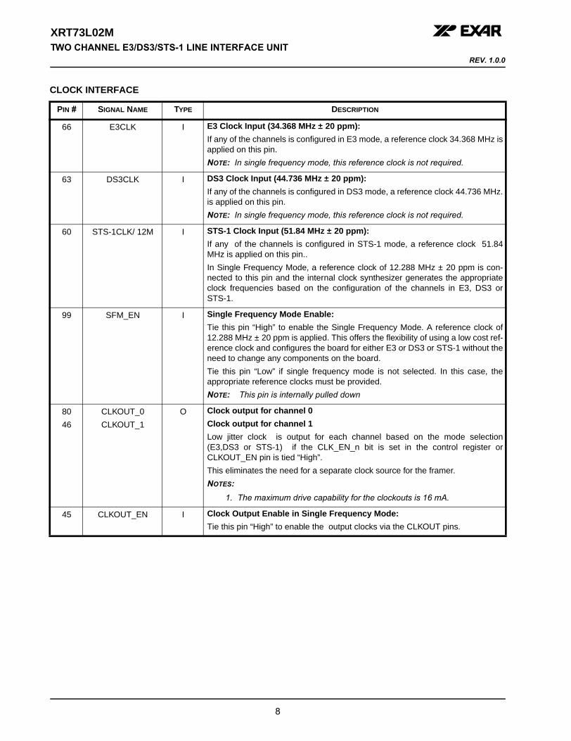
CLOCK INTERFACE
PIN # SIGNAL NAME TYPE DESCRIPTION
66 E3CLK I E3 Clock Input (34.368 MHz ± 20 ppm):
If any of the channels is configured in E3 mode, a reference clock 34.368 MHz isapplied on this pin.
NOTE: In single frequency mode, this reference clock is not required.
63 DS3CLK I DS3 Clock Input (44.736 MHz ± 20 ppm):
If any of the channels is configured in DS3 mode, a reference clock 44.736 MHz.is applied on this pin.
NOTE: In single frequency mode, this reference clock is not required.
60 STS-1CLK/ 12M I STS-1 Clock Input (51.84 MHz ± 20 ppm):
If any of the channels is configured in STS-1 mode, a reference clock 51.84MHz is applied on this pin..
In Single Frequency Mode, a reference clock of 12.288 MHz ± 20 ppm is con-nected to this pin and the internal clock synthesizer generates the appropriateclock frequencies based on the configuration of the channels in E3, DS3 orSTS-1.
99 SFM_EN I Single Frequency Mode Enable:
Tie this pin “High” to enable the Single Frequency Mode. A reference clock of12.288 MHz ± 20 ppm is applied. This offers the flexibility of using a low cost ref-erence clock and configures the board for either E3 or DS3 or STS-1 without theneed to change any components on the board.
Tie this pin “Low” if single frequency mode is not selected. In this case, theappropriate reference clocks must be provided.
NOTE: This pin is internally pulled down
80
46
CLKOUT_0
CLKOUT_1
O Clock output for channel 0
Clock output for channel 1
Low jitter clock is output for each channel based on the mode selection(E3,DS3 or STS-1) if the CLK_EN_n bit is set in the control register orCLKOUT_EN pin is tied “High”.
This eliminates the need for a separate clock source for the framer.
NOTES:1. The maximum drive capability for the clockouts is 16 mA.
45 CLKOUT_EN I Clock Output Enable in Single Frequency Mode:
Tie this pin “High” to enable the output clocks via the CLKOUT pins.
8

xr XRT73L02MTWO CHANNEL E3/DS3/STS-1 LINE INTERFACE UNIT
REV. 1.0.0
CONTROL AND ALARM INTERFACE
PIN # SIGNAL NAME TYPE DESCRIPTION
73
53
MRING_0
MRING_1
I Monitor Ring Input - Channel 0:
Monitor Ring Input - Channel 1:
The bipolar line output signal from TRING_n is connected to this pin via a 270 Ωresistor to check for line driver failure. NOTE: This pin is internally pulled "High".
72
54
MTIP_0
MTIP_1
I Monitor Tip Input - Channel 0:
Monitor Tip Input - Channel 1:
The bipolar line output signal from TTIP_n is connected to this pin via a 270-ohm resistor to check for line driver failure.
NOTE: This pin is internally pulled "High".
79
47
DMO_0
DMO_1
O Drive Monitor Output - Channel 0:
Drive Monitor Output - Channel 1:
If MTIP_n and MRING_n has no transition pulse for 128 ± 32 TxCLK_n cycles,DMO_n goes “High” to indicate the driver failure. DMO_n output stays “High”until the next AMI signal is detected.
94
33
RLOS_0
RLOS_1
O Receive Loss of Signal Output Indicator - Channel 0:
Receive Loss of Signal Output Indicator - Channel 1:
This output pin toggles "High" if the receiver has detected a Loss of Signal Con-dition.
The criteria for declaring /clearing an LOS Condition depends upon whether it isoperating in the E3 or STS-1/DS3 Mode.
95
32
RLOL_0
RLOL_1
O Receive Loss of Lock Output Indicator - Channel 0:
Receive Loss of Lock Output Indicator - Channel 1:
This output pin toggles "High" if a Loss of Lock Condition is detected. LOL(Loss of Lock) condition occurs if the recovered clock frequency deviates fromthe Reference Clock frequency (available at either E3CLK or DS3CLK or STS-1CLK input pins) by more than 0.5%.
11 RXA **** External Resistor of 3 K Ω ± 1%. Should be connected between RxA and RxB for internal bias.
12 RXB **** External Resistor of 3K Ω ±1%. Should be connected between RxA and RxB for internal bias.
98 ICT I In-Circuit Test Input:
Setting this pin "Low" causes all digital and analog outputs to go into a high-impedance state to allow for in-circuit testing. For normal operation, tie this pin"High".
NOTE: This pin is internally pulled “High".
96 TEST **** Factory Test Pin
NOTE: This pin must be connected to GND for normal operation.
9

XRT73L02M xrTWO CHANNEL E3/DS3/STS-1 LINE INTERFACE UNIT REV. 1.0.0
28 LOSMUT/INT
I/O Hardware Mode: MUTE-upon-LOS Enable Input Host Mode: Interrupt Ouput:In Hardware Mode, setting pin “High” configures all the channels to Mute therecovered data on the RPOS_n and RNEG_n whenever one of the channelsdeclares an LOS condition. RPOS_n and RNEG_n outputs are pulled “Low”.Muting of the output data can be configured/controlled on a per channel basis inHost Mode.NOTE: If the XRT73L02M is configured in HOST mode, this pin functions as INT pin (please refer to the pin description for the Microprocessor Interface).
422
LLB_0LLB_1
I Local Loop-back - Channel 0:Local Loop-back - Channel 1:This input pin along with RLB_n configures different Loop-Back modes. A "High" on this pin with RLB_n set to "Low" configures Channel_n to operate inthe Analog Local Loop-back Mode.A "High" on this pin with RLB_n set to "High" configures Channel_n to operatein the Digital Local Loop-back Mode.NOTE: This input pin is ignored and should be connected to GND if operating inthe HOST Mode.
521
RLB_0RLB_1
I Remote Loop-back - Channel 0:Remote Loop-back - Channel 1:This input pin along with LLB_n configures different Loop-Back modes.A "High" on this pin with LLB_n set to “Low" configures Channel_n to operate inthe Remote Loop-back Mode.A "High" on this pin with LLB_n set to "High" configures Channel_n to operatein the Digital Local Loop-back Mode.
NOTE: This input pin is ignored and should be connected to GND when operat-ing in the HOST Mode.
CONTROL AND ALARM INTERFACE
RLB_n
0
0
Loopback Mode
Normal Operation
Analog Local
LLB_n
0
1
1
1
Remote
Digital
0
1
10

xr XRT73L02MTWO CHANNEL E3/DS3/STS-1 LINE INTERFACE UNIT
REV. 1.0.0
MODE SELECT
PIN # SIGNAL NAME TYPE DESCRIPTION
2
24
E3_0
E3_1
I E3 Mode Select Input A "High" on this pin configures in E3 mode. A "Low" on this pin configures in either STS-1 or DS3 mode depending on thesettings on pins 3 and 23..NOTES:
1. This pin is internally pulled down2. This pin is ignored if configured to operate in HOST mode.
3
23
STS1/DS3 _0
STS1/DS3 _1
I STS-1/DS3 Select Input A “High” on these pins configures in STS-1 mode.A “Low” on these pins configures in DS3 mode.These pins are ignored if the E3_n pins are set to “High”. NOTES:
1. This pin is internally pulled down2. This pin is ignored if configured to operate in HOST mode.
26 HOST/HW I Host/Hardware Mode:
Tie this pin “High” to configure in Host mode and “Low” for Hardware mode.
100 SR/DR I Single-Rail/Dual-Rail Select:Setting this “High” configures both the Transmitter and Receiver to operate inSingle-rail mode and also enables the B3ZS/HDB3 Encoder and Decoder. InSingle-rail mode, TNEG_n pin should be grounded.Setting this “Low” configures both the Transmitter and Receiver to operate inDual-rail mode and disables the B3ZS/HDB3 Encoder and Decoder. NOTE: This pin is internally pulled down.
MICROPROCESSOR SERIAL INTERFACE - (HOST MODE)
PIN # SIGNAL NAME TYPE DESCRIPTION
29 CSRxCLKINV
I Microprocessor Serial Interface - Chip Select Tie this “Low” to enable the communication with the Microprocessor Serial Inter-face.NOTE: If configured in Hardware Mode, this pin functions as RxClkINV.
30 SCLKTxCLKINV
I Serial Interface Clock InputThe data on the SDI pin is sampled on the rising edge of this signal. Additionally,during Read operations the Microprocessor Serial Interface updates the SDOoutput on the falling edge of this signal.NOTE: If configured in Hardware Mode, this pin functions as TxClkINV.
11

XRT73L02M xrTWO CHANNEL E3/DS3/STS-1 LINE INTERFACE UNIT REV. 1.0.0
31 SDIRxON
I Serial Data Input:Data is serially input through this pin.The input data is sampled on the rising edge of the SClk. .NOTES:
1. This pin is internally pulled down2. If configured in Hardware Mode, this pin functions as RxON.
27 SDORxMON
I/O Serial Data Output:This pin serially outputs the contents of the specified Command Register duringRead Operations. The data is updated on the falling edge of the SClk and thispin is tri-stated upon completion of data transfer.NOTE: If configured in Hardware Mode, this pin functions as RxMON.
97 RESET I Register Reset:Setting this input pin "Low" causes to reset the contents of the Command Reg-isters to their default settings and default operating configurationNOTE: This pin is internally pulled up.
28 INTLOSMUT
I/O INTERRUPT Output:A transition to “Low” indicates that an interrupt has been generated. The inter-rupt function can be disabled by setting the interrupt enable bit to “0” in theChannel Control Register.NOTES:
1. In Hardware mode, this pin functions as LOSMUT.2. This pin will remain asserted “Low” until the interrupt is serviced.
MICROPROCESSOR SERIAL INTERFACE - (HOST MODE)
PIN # SIGNAL NAME TYPE DESCRIPTION
ANALOG POWER AND GROUND
PIN # SIGNAL NAME TYPE DESCRIPTION
84 TxAVDD_0 **** Transmitter Analog 3.3 V ± 5% VDD - Channel 0
43 TxAVDD_1 **** Transmitter Analog 3.3 V ± 5% VDD - Channel 1
83 TxAGND_0 **** Transmitter Analog GND - Channel 0
44 TxAGND_1 **** Transmitter Analog GND - Channel 1
6 RxAVDD_0 **** Receiver Analog 3.3 V ± 5% VDD - Channel 0
20 RxAVDD_1 **** Receiver Analog 3.3 V ± 5% VDD - Channel 1
7 RxAGND_0 **** Receiver Analog GND - Channel_0
19 RxAGND_1 **** Receive Analog GND - Channel 1
86 AVDD_0 **** Analog 3.3 V ± 5% VDD - Channel 0
41 AVDD_1 **** Analog 3.3 V ± 5% VDD - Channel 1
85 AGND_0 **** Analog GND - Channel 0
42 AGND_1 **** Analog GND - Channel 1
13 AVDD **** Analog 3.3 V ± 5% VDD
12

xr XRT73L02MTWO CHANNEL E3/DS3/STS-1 LINE INTERFACE UNIT
REV. 1.0.0
10 AGND **** Analog GND
14 AGND **** Analog GND
15 AGND **** Analog GND
16 AGND **** Analog GND
ANALOG POWER AND GROUND
PIN # SIGNAL NAME TYPE DESCRIPTION
DIGITAL POWER AND GROUND
PIN # SIGNAL NAME TYPE DESCRIPTION
69 TxVDD_0 **** Transmitter 3.3 V ± 5% VDD Channel 0
57 TxVDD_1 **** Transmitter 3.3 V ± 5% VDD Channel 1
68 TxGND_0 **** Transmitter GND - Channel 0
58 TxGND_1 **** Transmitter GND - Channel 1
89 RxDVDD_0 **** Receiver 3.3 V ± 5% VDD - Channel 0
38 RxDVDD_1 **** Receiver 3.3 V ± 5% VDD - Channel 1
90 RxDGND_0 **** Receiver Digital GND - Channel 0
37 RxDGND_1 **** Receiver Digital GND - Channel 1
87 DVDD_0 **** 3.3 V ± 5% VDD - Channel 0
40 DVDD_1 **** 3.3 V ± 5% VDD - Channel 188
88 DGND_0 **** Digital GND - Channel 0
39 DGND_1 **** Digital GND - Channel 1
61 DVDD **** Digital VDD 3.3.v ± 5%
62 DVDD **** Digital VDD 3.3.v ± 5%
67 DVDD **** Digital VDD 3.3.v ± 5%
59 DGND **** Digital GND
64 DGND **** Digital GND
65 DGND **** Digital GND
13

XRT73L02M xrTWO CHANNEL E3/DS3/STS-1 LINE INTERFACE UNIT REV. 1.0.0
1.0 ELECTRICAL CHARACTERISTICS
NOTES:1. Exposure to or operating near the Min or Max val-
ues for extended period may cause permanent fail-ure and impair reliability of the device.
2. ESD testing method is per MIL-STD-883D,M-3015.7
NOTES:1. Not applicable for pins with pull-up or pull-down
resistors.
2. The Digital inputs and outputs are TTL 5V compli-ant.
TABLE 1: ABSOLUTE MAXIMUM RATINGS
SYMBOL PARAMETER MIN MAX UNITS COMMENTS
VDD Supply Voltage -0.5 6.0 V Note 1
VIN Input Voltage at any Pin -0.5 5+0.5 V Note 1
IIN Input current at any pin 100 mA Note 1
STEMP Storage Temperature -65 150 0C Note 1
ATEMP Ambient Operating Temperature -40 85 0C linear airflow 0 ft./min
ThetaJA Thermal Resistance 35 0C/W linear air flow 0ft/min
ThetaJC 6 0C/W
MLEVL Exposure to Moisture 5 level EIA/JEDECJESD22-A112-A
ESD ESD Rating 2000 V Note 2
TABLE 2: DC ELECTRICAL CHARACTERISTICS:
SYMBOL PARAMETER MIN. TYP. MAX. UNITS
DVDD Digital Supply Voltage 3.135 3.3 3.465 V
AVDD Analog Supply Voltage 3.135 3.3 3.465 V
ICC Supply current requirement 100 210 325 mA
PDD Power Dissipation 700 900 mW
VIL Input Low Voltage 0.8 V
VIH Input High Voltage 2.0 5.0 V
VOL Output Low Voltage, IOUT = - 4mA 0.4 V
VOH Output High Voltage, IOUT = 4 mA 2.4 V
IL Input Leakage Current1 ±10 µA
CI Input Capacitance 10 pF
CL Load Capacitance 10 pF
14
xr XRT73L02MTWO CHANNEL E3/DS3/STS-1 LINE INTERFACE UNIT
REV. 1.0.0
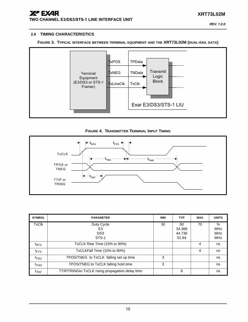
2.0 TIMING CHARACTERISTICS
FIGURE 3. TYPICAL INTERFACE BETWEEN TERMINAL EQUIPMENT AND THE XRT73L02M (DUAL-RAIL DATA)
TerminalEquipment
(E3/DS3 or STS-1Framer)
Exar E3/DS3/STS-1 LIU
TransmitLogicBlock
TxPOS
TxNEG
TxLineClk
TPData
TNData
TxClk
FIGURE 4. TRANSMITTER TERMINAL INPUT TIMING
TPOS orTNEG
TTIP orTRING
TxCLKtTSU tTHO
tRTX tFTX
tTDY
SYMBOL PARAMETER MIN TYP MAX UNITS
TxClk Duty Cycle E3
DS3STS-1
30 5034.36844.73651.84
70 %MHzMHzMHz
tRTX TxCLK Rise Time (10% to 90%) 4 ns
tFTX TxCLKFall Time (10% to 90%) 4 ns
tTSU TPOS/TNEG to TxCLK falling set up time 3 ns
tTHO TPOS/TNEG to TxCLK falling hold time 3 ns
tTDY TTIP/TRINGto TxCLK rising propagation delay time 8 ns
15

XRT73L02M xrTWO CHANNEL E3/DS3/STS-1 LINE INTERFACE UNIT REV. 1.0.0
FIGURE 5. RECEIVER DATA OUTPUT AND CODE VIOLATION TIMING
RxCLK
tRRX tFRX
RPOS orRNEG
LCV
tLCVO
tCO
SYMBOL PARAMETER MIN TYP MAX UNITS
RxClk Duty CycleE3
DS3STS-1
45 5034.36844.73651.84
55 %MHzMHzMHz
tRRX RxCLK rise time (10% o 90%) 2 4 ns
tFRX RxCLKfalling time (10% to 90%) 2 4 ns
tCO RxCLKto RPOS/RNEG delay time 4 ns
tLCVO RxCLK to rising edge of LCV output delay 2.5 ns
FIGURE 6. TRANSMIT INTERFACE CIRCUIT FOR E3, DS3 AND STS-1 RATES
3 kΩ
+ 1
%
TTIP(n)
TRING(n)
XRT73L02M (0nly one channel shown)
1:1
R375Ω
TxPOS(n)TxNEG(n)
TxLineClk(n)
TPOS(n)TNEG(n)TxCLK(n)
RxB
RxA31.6Ω + 1%
31.6Ω +1%
R1
R2
16
xr XRT73L02MTWO CHANNEL E3/DS3/STS-1 LINE INTERFACE UNIT
REV. 1.0.0
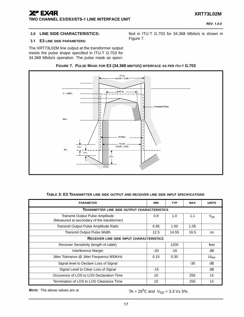
3.0 LINE SIDE CHARACTERISTICS:
3.1 E3 LINE SIDE PARAMETERS:
The XRT73L02M line output at the transformer outputmeets the pulse shape specified in ITU-T G.703 for34.368 Mbits/s operation. The pulse mask as speci-
fied in ITU-T G.703 for 34.368 Mbits/s is shown inFigure 7.
NOTE: The above values are at TA = 250C and VDD = 3.3 V± 5%.
FIGURE 7. PULSE MASK FOR E3 (34.368 MBITS/S) INTERFACE AS PER ITU-T G.703
0%
50%
V = 100%
14.55ns
Nominal Pulse
12.1ns(14.55 - 2.45)
17 ns(14.55 + 2.45)
8.65 ns
10%
10%
20%
TABLE 3: E3 TRANSMITTER LINE SIDE OUTPUT AND RECEIVER LINE SIDE INPUT SPECIFICATIONS
PARAMETER MIN TYP MAX UNITS
TRANSMITTER LINE SIDE OUTPUT CHARACTERISTICS
Transmit Output Pulse Amplitude (Measured at secondary of the transformer)
0.9 1.0 1.1 Vpk
Transmit Output Pulse Amplitude Ratio 0.95 1.00 1.05
Transmit Output Pulse Width 12.5 14.55 16.5 ns
RECEIVER LINE SIDE INPUT CHARACTERISTICS
Receiver Sensitivity (length of cable) 1200 feet
Interference Margin -20 -16 dB
Jitter Tolerance @ Jitter Frequency 800KHz 0.15 0.30 UIPP
Signal level to Declare Loss of Signal -35 dB
Signal Level to Clear Loss of Signal -15 dB
Occurence of LOS to LOS Declaration Time 10 255 UI
Termination of LOS to LOS Clearance Time 10 255 UI
17

XRT73L02M xrTWO CHANNEL E3/DS3/STS-1 LINE INTERFACE UNIT REV. 1.0.0
FIGURE 8. BELLCORE GR-253 CORE TRANSMIT OUTPUT PULSE TEMPLATE FOR SONET STS-1 APPLICATIONS
STS-1 Pulse Template
-0.2
0
0.2
0.4
0.6
0.8
1
1.2
-1-0.
9-0.
8-0.
7-0.
6-0.
5-0.
4-0.
3-0.
2-0.
1 00.1 0.2 0.3 0.4 0.5 0.6 0.7 0.8 0.9
11.1 1.2 1.3 1.4
Time, in UI
Nor
mal
ized
Am
plitu
de
Lower Curve
Upper Curve
TABLE 4: STS-1 PULSE MASK EQUATIONS
TIME IN UNIT INTERVALS NORMALIZED AMPLITUDE
LOWER CURVE
-0.85 < T < -0.38 - 0.03
-0.38 < T < 0.36
0.36 < T < 1.4 - 0.03
UPPER CURVE
-0.85 < T < -0.68 0.03
-0.68 < T < 0.26
0.26 < T < 1.4 0.1 + 0.61 x e-2.4[T-0.26]
0.5 1π2--- 1
T0.18----------
0.03–+sin+
0.5 1π2--- 1
T0.34----------
0.03+ +sin+
18

xr XRT73L02MTWO CHANNEL E3/DS3/STS-1 LINE INTERFACE UNIT
REV. 1.0.0
NOTE: The above values are at
TA = 250C and VDD = 3.3 V ± 5%.
TABLE 5: STS-1 TRANSMITTER LINE SIDE OUTPUT AND RECEIVER LINE SIDE INPUT SPECIFICATIONS (GR-253)
PARAMETER MIN TYP MAX UNITS
TRANSMITTER LINE SIDE OUTPUT CHARACTERISTICS
Transmit Output Pulse Amplitude (measured with TxLEV = 0)
0.75 Vpk
Transmit Output Pulse Amplitude(measured with TxLEV = 1)
0.98 Vpk
Transmit Output Pulse Width 8.6 9.65 10.6 ns
Transmit Output Pulse Amplitude Ratio 0.9 1.0 1.1
RECEIVER LINE SIDE INPUT CHARACTERISTICS
Receiver Sensitivity (length of cable) 900 1100 feet
Jitter Tolerance @ Jitter Frequency 400 KHz 0.15 0.79 UIpp
FIGURE 9. TRANSMIT OUPUT PULSE TEMPLATE FOR DS3 AS PER BELLCORE GR-499
DS3 Pulse T emplate
-0.2
0
0.2
0.4
0.6
0.8
1
1.2
-1-0.9 -0.8 -0.7 -0.6 -0.5 -0.4 -0.3 -0.2 -0.1 0
0.1 0.2 0.3 0.4 0.5 0.6 0.7 0.8 0.9 11.1 1.2 1.3 1.4
Time, in UI
Nor
mal
ized
Am
plitu
de
Lower Curve
Upper Curve
19

XRT73L02M xrTWO CHANNEL E3/DS3/STS-1 LINE INTERFACE UNIT REV. 1.0.0
NOTE: The above values are at
TA = 250C and VDD = 3.3V ± 5%.
TABLE 6: DS3 PULSE MASK EQUATIONS
TIME IN UNIT INTERVALS NORMALIZED AMPLITUDE
LOWER CURVE
-0.85 < T < -0.36 - 0.03
-0.36 < T < 0.36
0.36 < T < 1.4 - 0.03
UPPER CURVE
-0.85 < T < -0.68 0.03
-0.68 < T < 0.36
0.36 < T < 1.4 0.08 + 0.407 x e-1.84[T-0.36]
0.5 1π2--- 1
T0.18----------
0.03–+sin+
0.5 1π2--- 1
T0.34----------
0.03+ +sin+
TABLE 7: DS3 TRANSMITTER LINE SIDE OUTPUT AND RECEIVER LINE SIDE INPUT SPECIFICATIONS (GR-499)
PARAMETER MIN TYP MAX UNITS
TRANSMITTER LINE SIDE OUTPUT CHARACTERISTICS
Transmit Output Pulse Amplitude (measured with TxLEV = 0)
0.75 Vpk
Transmit Output Pulse Amplitude(measured with TxLEV = 1)
1.0 Vpk
Transmit Output Pulse Width 10.10 11.18 12.28 ns
Transmit Output Pulse Amplitude Ratio 0.9 1.0 1.1
RECEIVER LINE SIDE INPUT CHARACTERISTICS
Receiver Sensitivity (length of cable) 900 1100 feet
Jitter Tolerance @ 400 KHz (Cat II) 0.60 UIpp
20

xr XRT73L02MTWO CHANNEL E3/DS3/STS-1 LINE INTERFACE UNIT
REV. 1.0.0
FIGURE 10. MICROPROCESSOR SERIAL INTERFACE STRUCTURE
D0 D1 D2 D7D6D5D4D3High Z
SDO
A0 D0R/W D10A5A4A3A2A1 D7D6D5D4D3D2SDI
1 2 3 4 5 6 7 8 9 10 11 12 13 14 15 16SClk
CS
High Z
FIGURE 11. TIMING DIAGRAM FOR THE MICROPROCESSOR SERIAL INTERFACE
SDI R/W A1A0
CS
SCLK
CS
SCLK
SDI
SDO D0 D1 D2 D7
t21
t22 t23
t24 t25
t26
t27
t28
t29 t30
t31 t32
Hi-Z
Hi-Z
TABLE 8: MICROPROCESSOR SERIAL INTERFACE TIMINGS ( TA = 250C, VDD=3.3V± 5% AND LOAD = 10PF)
SYMBOL PARAMETER MIN. TYP. MAX UNITS
t21 CS Low to Rising Edge of SClk 5 ns
t22 SDI to Rising Edge of SClk 5 ns
t23 SDI to Rising Edge of SClk Hold Time 5 ns
21

XRT73L02M xrTWO CHANNEL E3/DS3/STS-1 LINE INTERFACE UNIT REV. 1.0.0
t24 SClk "Low" Time 25 ns
t25 SClk "High" Time 25 ns
t26 SClk Period 50 ns
t27 Falling Edge of SClk to rising edge of CS 0 ns
t28 CS "Inactive" Time 50 ns
t29 Falling Edge of SClk to SDO Valid Time 20 ns
t30 Falling Edge of SClk to SDO Invalid Time 10 ns
t31 Rising edge of CS to High Z 10 ns
t32 Rise/Fall time of SDO Output 5 ns
TABLE 8: MICROPROCESSOR SERIAL INTERFACE TIMINGS ( TA = 250C, VDD=3.3V± 5% AND LOAD = 10PF)
SYMBOL PARAMETER MIN. TYP. MAX UNITS
22

xr XRT73L02M
TWO CHANNEL E3/DS3/STS-1 LINE INTERFACE UNIT
REV. 1.0.0
FUNCTIONAL DESCRIPTION:Figure 1 shows the functional block diagram of the device. Each channel can be independently configured ei-ther by Hardware Mode or by Host Mode to support E3, DS3 or STS-1 modes. A detailed operation of eachsection is described below.
Each channel consists of the following functional blocks:
4.0 THE TRANSMITTER SECTION: The Transmitter Section, within each Channel, accepts TTL/CMOS level signals from the Terminal Equipmentin selectable data formats.
• Convert the CMOS level B3ZS or HDB3 encoded data into pulses with shapes that are compliant with thevarious industry standard pulse template requirements. Figures 7, 8 and 9 illustrate the pulse templaterequirements.
• Encode the un-encoded NRZ data into either B3ZS format (for DS3 or STS-1) or HDB3 format (for E3) andconvert to pulses with shapes and width that are compliant with industry standard pulse template require-ments. Figures 7, 8 and 9 illustrate the pulse template requirements.
• In Single-Rail or un-encoded Non-Return-to-Zero (NRZ) mode, data is input via TPOS_n pins while TNEG_npins must be grounded. The NRZ or Single-Rail mode is selected when the SR/DR input pin is “High” (inHardware Mode) or bit 0 of channel control register is “1” (in Host Mode). Figure 12 illustrates the Single-Railor NRZ format.
• In Dual-Rail mode, data is input via TPOS_n and TNEG_n pins. TPOS_n contains positive data andTNEG_n contains negative data. The SR/DR input pin = “Low” (in Hardware Mode) or bit 0 of channel regis-ter = “0” (in Host Mode) enables the Dual-Rail mode. Figure 13 illustrates the Dual-Rail data format.
FIGURE 12. SINGLE-RAIL OR NRZ DATA FORMAT (ENCODER AND DECODER ARE ENABLED)
FIGURE 13. DUAL-RAIL DATA FORMAT (ENCODER AND DECODER ARE DISABLED)
TxClk
TPData
Data 1 1 0
TxClk
TPData
TNData
Data 1 1 0
23

XRT73L02M xr
TWO CHANNEL E3/DS3/STS-1 LINE INTERFACE UNIT REV. 1.0.0
4.0.1 TRANSMIT CLOCK:The Transmit Clock applied via TxClk_n pins, for the selected data rate (for E3 = 34.368 MHz, DS3 = 44.736MHz or STS-1 = 51.84 MHz), is duty cycle corrected by the internal PLL circuit to provide a 50% duty cycleclock to the pulse shaping circuit. This allows a 30% to 70% duty cycle Transmit Clock to be supplied.
4.0.2 B3ZS/HDB3 ENCODER:When the Single-Rail (NRZ) data format is selected, the Encoder Block encodes the data into either B3ZS for-mat (for either DS3 or STS-1) or HDB3 format (for E3).
4.0.2.1 B3ZS Encoding:An example of B3ZS encoding is shown in Figure 14. If the encoder detects an occurrence of three consecu-tive zeros in the data stream, it is replaced with either B0V or 00V, where ‘B’ refers to Bipolar pulse that is com-pliant with the Alternating polarity requirement of the AMI (Alternate Mark Inversion) line code and ‘V’ refers toa Bipolar Violation (e.g., a bipolar pulse that violates the AMI line code). The substitution of B0V or 00V ismade so that an odd number of bipolar pulses exist between any two consecutive violation (V) pulses. Thisavoids the introduction of a DC component into the line signal.
4.0.2.2 HDB3 Encoding:An example of the HDB3 encoding is shown in Figure 15. If the HDB3 encoder detects an occurrence of fourconsecutive zeros in the data stream, then the four zeros are substituted with either 000V or B00V pattern. Thesubstitution code is made in such a way that an odd number of bipolar (B) pulses exist between any consecu-tive V pulses. This avoids the introduction of DC component into the analog signal.
NOTES: 1. When Dual-Rail data format is selected, the B3ZS/HDB3 Encoder is automatically disabled. 2. In Dual-Rail format, the Bipolar Violations in the incoming data stream is converted to valid data pulses.
3. Encoder and Decoder is enabled only in Single-Rail mode.
FIGURE 14. B3ZS ENCODING FORMAT
FIGURE 15. HDB3 ENCODING FORMAT
0 0 01
1
1
1111
VB
V1
00 00 0 000000
000 0 0V
B V
00 0
TClk
LineSignal
TPDATA
000 0 01
1
1
1111
VB
V1
00 00 0 000000
00 0 0V
B
00 0
TClk
LineSignal
TPDATA
24

xr XRT73L02M
TWO CHANNEL E3/DS3/STS-1 LINE INTERFACE UNIT
REV. 1.0.0
4.0.3 TRANSMIT PULSE SHAPER:The Transmit Pulse Shaper converts the B3ZS encoded digital pulses into a single analog Alternate Mark In-version (AMI) pulse that meet the industry standard mask template requirements for STS-1 and DS3. See Fig-ures 8 and 9.
For E3 mode, the pulse shaper converts the HDB3 encoded pulses into a single full amplitude square shapedpulse with very little slope. This is illustrated in Figure 7.
The Pulse Shaper Block also includes a Transmit Build Out Circuit, which can either be disabled or enabled bysetting the TxLEV_n input pin “High” or “Low” (in Hardware Mode) or setting the TxLEV_n bit to “1” or “0” in thecontrol register (in Host Mode).
For DS3/STS-1 rates, the Transmit Build Out Circuit is used to shape the transmit waveform that ensures thattransmit pulse template requirements are met at the Cross-Connect system. The distance between the trans-mitter output and the Cross-Connect system can be between 0 to 450 feet.
For E3 rate, since the output pulse template is measured at the secondary of the transformer and since there isno Cross-Connect system pulse template requirements, the Transmit Build Out Circuit is always disabled.
4.0.3.1 Guidelines for using Transmit Build Out Circuit:If the distance between the transmitter and the DSX3 or STSX-1, Cross-Connect system, is less than 225 feet,enable the Transmit Build Out Circuit by setting the TxLEV_n input pin “Low” (in Hardware Mode) or setting theTxLEV_n control bit to “0” (in Host Mode).
If the distance between the transmitter and the DSX3 or STSX-1 is greater than 225 feet, disable the TransmitBuild Out Circuit.
4.0.3.2 Interfacing to the line:The differential line driver increases the transmit waveform to appropriate level and drives into the 75Ω load asshown in Figure 6.
4.0.4 Transmit Drive Monitor:This feature is used for monitoring the transmit line for occurrence of fault conditions such as a short circuit onthe line or a defective line driver.
To activate this function, connect MTIP_n pins to the TTIP_n lines via a 270 Ω resistor and MRing_n pins toTRING_n lines via 270 Ω resistor as shown in Figure 16.
FIGURE 16. TRANSMIT DRIVER MONITOR SET-UP.
3kΩ
+ 1
%
TTIP(n)
TRING(n)
XRT73L02M (0nly one channel shown)
1:1
R375ΩTxPOS(n)
TxNEG(n)TxLineClk(n)
TPOS(n)TNEG(n)TxCLK(n)
RxB
RxA
31.6Ω + 1%
31.6Ω +1%
R1
R2
MRING(n)
MTIP(n)
R5 270Ω
R4 270Ω
25

XRT73L02M xr
TWO CHANNEL E3/DS3/STS-1 LINE INTERFACE UNIT REV. 1.0.0
When the MTIP_n and MRING_n are connected to the TTIP_n and TRING_n lines, the drive monitor circuitmonitors the line for transitions. The DMO_n (Drive Monitor Output) will be asserted “Low” as long as the tran-sitions on the line are detected via MTIP_n and MRING_n.
If no transitions on the line are detected for 128 ± 32 TxClk_n periods, the DMO_n output toggles “High” andwhen the transitions are detected again, DMO_n toggles “Low”.
NOTES:
1. The Drive Monitor Circuit is only for diagnostic purpose and does not have to be used to operate the transmitter.2. With TxMON pin “High”, MTIP and MRING will be internally connected to TTIP and TRING for self-monitoring.
4.0.5 TRANSMITTER SECTION ON/OFF:The transmitter section of each channel can either be turned on or off. To turn on the transmitter, set the inputpin TxON to “High” (in Hardware Mode) or in Host Mode set the TxON_n control bits and tie the TxON pins“High”
When the transmitter is turned off, TTIP_n and TRING_n are tri-stated.
NOTES:1. This feature provides support for Redundancy.
2. If configured in Host mode, to permit a system designed for redundancy to quickly shut-off the defective line cardand turn on the back-up line card, setting the TxON_n control bits transfers the control to TxON pins.
5.0 THE RECEIVER SECTION:This section describes the detailed operation of the various blocks in the receiver. The receiver recovers theTTL/CMOS level data from the incoming bipolar B3ZS or HDB3 encoded input pulses.
5.0.1 AGC/EQUALIZER:The Adaptive Gain Control circuit amplifies the incoming analog signal and compensates for the various flatlosses and also for the loss at one-half symbol rate. The AGC has a dynamic range of 30 dB.
The Equalizer restores the integrity of the signal and compensates for the frequency dependent attenuation upto 900 feet of coaxial cable (1300 feet for E3). The Equalizer also boosts the high frequency content of the sig-nal to reduce Inter-Symbol Interference (ISI) so that the slicer slices the signal at 50% of peak voltage to gen-erate Positive and Negative data.
The Equalizer can either be “IN” or “OUT” by setting the REQEN_n pin “High” or “Low” (in Hardware Mode) orsetting the REQEN_n control bit to “1” or “0” (in Host Mode).
RECOMMENDATIONS FOR EQUALIZER SETTINGS:
The Equalizer has two gain settings to provide optimum equalization. In the case of normally shaped DS3/STS-1 pulses (pulses that meet the template requirements) that has been driven through 0 to 900 feet of cable,the Equalizer can be left “IN” by setting the REQEN_n pin to “High” (in Hardware Mode) or setting theREQEN_n control bit to “1” (in Host Mode).
However, for square-shaped pulses such as E3 or for DS3/STS-1 high pulses (that does not meet the pulsetemplate requirements), it is recommended that the Equalizer be left “OUT” for cable length less than 300 feetby setting the REQEN_n pin “Low” (in Hardware Mode) or by setting the REQEN_n control bit to “0” (in HostMode).This would help to prevent over-equalization of the signal and thus optimize the performance in terms ofbetter jitter transfer characteristics.
NOTE: The results of extensive testing indicates that even when the Equalizer was left “IN” (REQEN_n = “HIGH”),regardless of the cable length, the integrity of the E3 signal was restored properly over 0 to 12 dB cable loss atIndustrial Temperature.
26

xr XRT73L02M
TWO CHANNEL E3/DS3/STS-1 LINE INTERFACE UNIT
REV. 1.0.0
The Equalizer also contain an additional 20 dB gain stage to provide the line monitoring capability of the resis-tively attenuated signals which may have 20dB flat loss. This capability can be turned on by setting theRxMON_n bits in the control register or by setting the RxMON pin “High”.
5.0.1.1 INTERFERENCE TOLERANCE:For E3 mode, ITU-T G.703 Recommendation specifies that the receiver be able to recover error-free clock anddata in the presence of a sinusoidal interfering tone signal. For DS3 and STS-1 modes, the same recommen-dation is being used. Figure 17 shows the configuration to test the interference margin for DS3/STS1. Figure18 shows the set up for E3.
FIGURE 17. INTERFERENCE MARGIN TEST SET UP FOR DS3/STS-1
FIGURE 18. INTERFERENCE MARGIN TEST SET UP FOR E3.
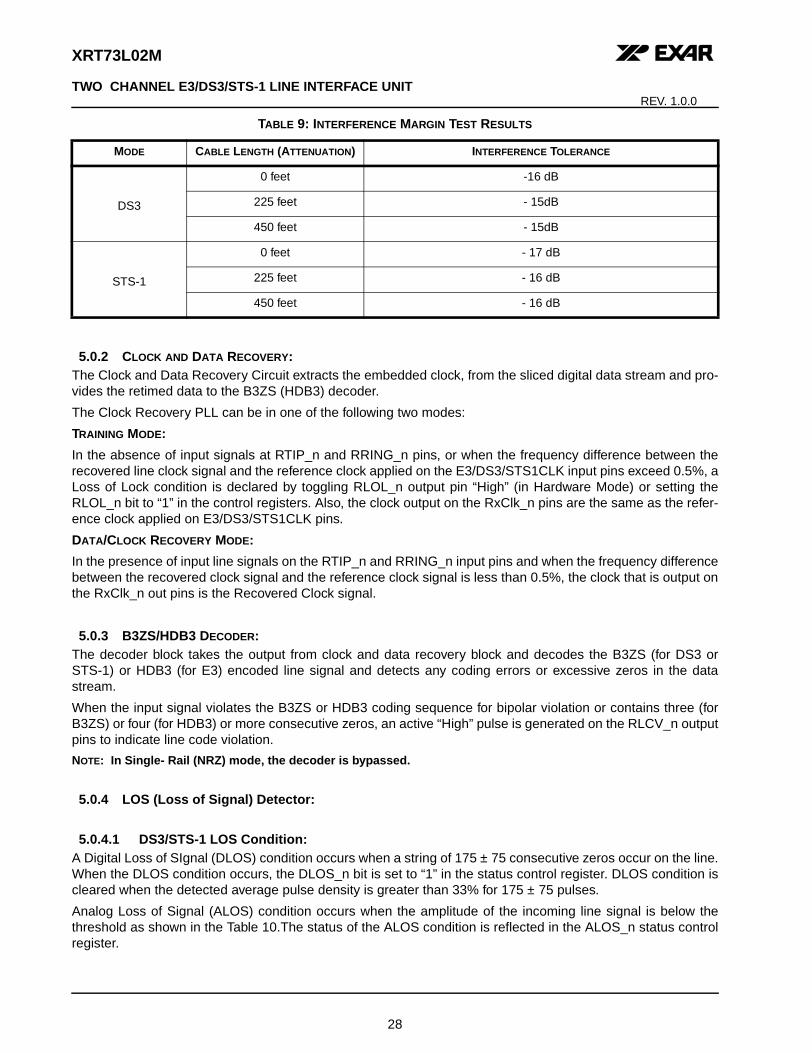
TABLE 9: INTERFERENCE MARGIN TEST RESULTS
MODE CABLE LENGTH (ATTENUATION) INTERFERENCE TOLERANCE
E30 dB - 17 dB
12 dB -15 dB
∑Test Equipment
Pattern Generator2 23 -1 PRBS
Sine WaveGenerator
N
S
0 to 900 feetCoaxial Cable
DUT(XRT73L02M)
Attenuator
DS3 = 22.368 MHzSTS-1 = 25.92 MHz
∑Test Equipment
Noise Generator2 23 -1 PRBS
Signal Source
N
S
0 to 12 dB Cable LossDUT
(XRT73L02M)
Attenuator 1 Attenuator 2
27
XRT73L02M xr
TWO CHANNEL E3/DS3/STS-1 LINE INTERFACE UNIT REV. 1.0.0
5.0.2 CLOCK AND DATA RECOVERY:The Clock and Data Recovery Circuit extracts the embedded clock, from the sliced digital data stream and pro-vides the retimed data to the B3ZS (HDB3) decoder.
The Clock Recovery PLL can be in one of the following two modes:
TRAINING MODE:
In the absence of input signals at RTIP_n and RRING_n pins, or when the frequency difference between therecovered line clock signal and the reference clock applied on the E3/DS3/STS1CLK input pins exceed 0.5%, aLoss of Lock condition is declared by toggling RLOL_n output pin “High” (in Hardware Mode) or setting theRLOL_n bit to “1” in the control registers. Also, the clock output on the RxClk_n pins are the same as the refer-ence clock applied on E3/DS3/STS1CLK pins.
DATA/CLOCK RECOVERY MODE:
In the presence of input line signals on the RTIP_n and RRING_n input pins and when the frequency differencebetween the recovered clock signal and the reference clock signal is less than 0.5%, the clock that is output onthe RxClk_n out pins is the Recovered Clock signal.
5.0.3 B3ZS/HDB3 DECODER:The decoder block takes the output from clock and data recovery block and decodes the B3ZS (for DS3 orSTS-1) or HDB3 (for E3) encoded line signal and detects any coding errors or excessive zeros in the datastream.
When the input signal violates the B3ZS or HDB3 coding sequence for bipolar violation or contains three (forB3ZS) or four (for HDB3) or more consecutive zeros, an active “High” pulse is generated on the RLCV_n outputpins to indicate line code violation.
NOTE: In Single- Rail (NRZ) mode, the decoder is bypassed.
5.0.4 LOS (Loss of Signal) Detector:
5.0.4.1 DS3/STS-1 LOS Condition:A Digital Loss of SIgnal (DLOS) condition occurs when a string of 175 ± 75 consecutive zeros occur on the line.When the DLOS condition occurs, the DLOS_n bit is set to “1” in the status control register. DLOS condition iscleared when the detected average pulse density is greater than 33% for 175 ± 75 pulses.
Analog Loss of Signal (ALOS) condition occurs when the amplitude of the incoming line signal is below thethreshold as shown in the Table 10.The status of the ALOS condition is reflected in the ALOS_n status controlregister.
DS3
0 feet -16 dB
225 feet - 15dB
450 feet - 15dB
STS-1
0 feet - 17 dB
225 feet - 16 dB
450 feet - 16 dB
TABLE 9: INTERFERENCE MARGIN TEST RESULTS
MODE CABLE LENGTH (ATTENUATION) INTERFERENCE TOLERANCE
28

xr XRT73L02M
TWO CHANNEL E3/DS3/STS-1 LINE INTERFACE UNIT
REV. 1.0.0
RLOS is the logical OR of the DLOS and ALOS states. When the RLOS condition occurs the RLOS_n outputpin is toggled “High” and the RLOS_n bit is set to “1” in the status control register.
DISABLING ALOS/DLOS DETECTION:For debugging purposes it is useful to disable the ALOS and/or DLOS detection. Setting both ALOSDIS_n andDLOSDIS_n bits disables the LOS detection on a per channel basis.
5.0.4.2 E3 LOS Condition:If the level of incoming line signal drops below the threshold as described in the ITU-T G.775 standard, theLOS condition is detected. Loss of signal level is defined to be between 15 and 35 dB below the normal level. Ifthe signal drops below 35 dB for 175 ± 75 consecutive pulse periods, LOS condition is declared. This is illus-trated in Figure 19.
TABLE 10: THE ALOS (ANALOG LOS) DECLARATION AND CLEARANCE THRESHOLDS FOR A GIVEN SETTING OF REQEN (DS3 AND STS-1 APPLICATIONS)
APPLICATION REQEN SETTING SIGNAL LEVEL TO DECLARE ALOS SIGNAL LEVEL TO CLEAR ALOS
DS3 0 <17 mV >70 mV
1 <20 mV >90 mV
STS-1 0 <20 mV >90 mV
1 <25 mV >115 mV
FIGURE 19. LOSS OF SIGNAL DEFINITION FOR E3 AS PER ITU-T G.775
0 dB
-12 dB
-15dB
-35dB
Maximum Cable Loss for E3
LOS Signal Must be Declared
LOS Signal Must be Cleared
LOS Signal may be Cleared or Declared
29

XRT73L02M xr
TWO CHANNEL E3/DS3/STS-1 LINE INTERFACE UNIT REV. 1.0.0
As defined in ITU-T G.775, an LOS condition is also declared between 10 and 255 UI (or E3 bit periods) afterthe actual time the LOS condition has occurred. The LOS condition is cleared within 10 to 255 UI after restora-tion of the incoming line signal. Figure 20 shows the LOS declaring and clearing conditions.
5.0.4.3 Muting the Recovered Data with LOS condition:When the LOS condition is declared, the clock recovery circuit locks into the reference clock applied to the E3/DS3/STS1CLK pin and output this clock on the RxClk_n output. In Single Frequency Mode (SFM), the clock re-covery locks into the rate clock generated and output this clock on the RxClk_n pins. The data on the RPOS_nand RNEG_n pins can be forced to zero by pulling the LOSMUT pin “High” (in Hardware Mode) or by settingthe LOSMUT_n bits in the individual channel control register to “1” (in Host Mode).
NOTE: When the LOS condition is cleared, the recovered data is output on RPOS_n and RNEG_n pins.
6.0 JITTER:
There are three fundamental parameters that describe circuit performance relative to jitter:
• Jitter Tolerance (Receiver)
• Jitter Transfer (Receiver/Transmitter)
• Jitter Generation
6.0.1 JITTER TOLERANCE - RECEIVER: Jitter tolerance is a measure of how well a Clock and Data Recovery unit can successfully recover data in thepresence of various forms of jitter. It is characterized by the amount of jitter required to produce a specified biterror rate. The tolerance depends on the frequency content of the jitter. Jitter Tolerance is measured as the jit-ter amplitude over a jitter spectrum for which the clock and data recovery unit achieves a specified bit error rate(BER). To measure the jitter tolerance as shown in Figure 21, jitter is introduced by the sinusoidal modulation ofthe serial data bit sequence.
FIGURE 20. LOSS OF SIGNAL DEFINITION FOR E3 AS PER ITU-T G.775.
Actual Occurrenceof LOS Condition
Line Signalis Restored
Time Range forLOS Declaration
Time Range forLOS Clearance
G.775Compliance
G.775Compliance
0 UI
10 UI
0 UI
10 UI 255 UI255 UI
RTIP/RRing
RLOS Output Pin
30

xr XRT73L02M
TWO CHANNEL E3/DS3/STS-1 LINE INTERFACE UNIT
REV. 1.0.0
Input jitter tolerance requirements are specified in terms of compliance with jitter mask which is represented asa combination of points.Each point corresponds to a minimum amplitude of sinusoidal jitter at a given jitter fre-quency.
6.0.1.1 DS3/STS-1 Jitter Tolerance Requirements:Bellcore GR-499 CORE, Issue 1, December 1995 specifies the minimum requirement of jitter tolerance for Cat-egory I and Category II. The jitter tolerance requirement for Category II is the most stringent. Figure 22 showsthe jitter tolerance curve as per GR-499 specification.
FIGURE 21. JITTER TOLERANCE MEASUREMENTS
FIGURE 22. INPUT JITTER TOLERANCE FOR DS3/STS-1
FREQSynthesizer
FREQSynthesizer
PatternGenerator
PatternGenerator DUT
XRT73L02M
DUTXRT73L02M Error
Detector
ErrorDetector
ModulationFreq.
Data
Clock
0.01 0.03
15
1.5
0.3 2 20
0.15
JITT
ER A
MPL
ITU
DE
(UI pp
)
JITTER FREQUENCY (kHz)
10
5
0.3
100
0.1
GR-253 STS-1
GR-499 Cat II
GR-499 Cat I
64
41
XRT73L02M
31

XRT73L02M xr
TWO CHANNEL E3/DS3/STS-1 LINE INTERFACE UNIT REV. 1.0.0
6.0.1.2 E3 Jitter Tolerance Requirements:ITU-T G.823 standard specifies that the clock and data recovery unit must be able to accommodate and toler-ate jitter up to certain specified limits. Figure 23 shows the tolerance curve.
As shown in the Figures 22 and 23 above, in the jitter tolerance measurement, the dark line indicates the mini-mum level of jitter that the E3/DS3/STS-1 compliant component must tolerate.
The Table 11 below shows the jitter amplitude versus the modulation frequency for various standards.
6.0.2 JITTER TRANSFER - RECEIVER/TRANSMITTER:Jitter Transfer function is defined as the ratio of jitter on the output relative to the jitter applied on the input ver-sus frequency.
FIGURE 23. INPUT JITTER TOLERANCE FOR E3
TABLE 11: JITTER AMPLITUDE VERSUS MODULATION FREQUENCY (JITTER TOLERANCE)
BIT RATE
(KB/S)STANDARD
INPUT JITTER AMPLITUDE (UI P-P) MODULATION FREQUENCY
A1 A2 A3 F1(HZ) F2(HZ) F3(KHZ) F4(KHZ) F5(KHZ)
34368 ITU-T G.823 1.5 0.15 - 100 1000 10 800 -
44736 GR-499 CORE Cat I
5 0.1 - 10 2.3k 60 300 -
44736 GR-499 CORE Cat II
10 0.3 - 10 669 22.3 300 -
51840 GR-253 CORE Cat II
15 1.5 0.15 10 30 300 2 20
0.1
1.5
1 10
JITT
ER A
MPL
ITU
DE
(UI pp
)
JITTER FREQUENCY (kHz)800
ITU-T G.82364
10
0.3
XRT73L02M
32

xr XRT73L02M
TWO CHANNEL E3/DS3/STS-1 LINE INTERFACE UNIT
REV. 1.0.0
There are two distinct characteristics of jitter transfer: i) jitter gain (jitter peaking) defined as the highest ratioabove 0dB; and ii) jitter transfer bandwidth.The overall jitter transfer bandwidth is controlled by a low bandwidthloop, typically using a voltage-controller crystal oscillator (VCXO).
The jitter transfer function is a ratio between the jitter output and jitter input for a component, or system oftenexpressed in dB. A negative dB jitter transfer indicates the element removed jitter. A positive dB jitter transferindicates the element added jitter. A zero dB jitter transfer indicates the element had no effect on jitter.
6.0.3 JITTER GENERATION:Jitter Generation is defined as the process whereby jitter appears at the output port of the digital equipment inthe absence of applied input jitter. Jitter Generation is measured by sending jitter free data to the clock and da-ta recovery circuit and measuring the amount of jitter on the output clock or the re-timed data. Since this is es-sentially a noise measurement, it requires a definition of bandwidth to be meaningful. The bandwidth is set ac-cording to the data rate. In general, the jitter is measured over a band of frequencies.
7.0 SERIAL HOST INTERFACE: A serial microprocessor interface is included in the XRT73L02M. The interface is generic and is designed tosupport the common microprocessors/microcontrollers. The XRT73L02M is configured in Host mode when theHOST/HW pin is tied “High”. The serial interface includes a serial clock (SClk), serial data input (SDI), serialdata output (SDO), chip select (CS) and interrupt output (INT). The serial interface timing is shown in Figure11.
The active low interrupt output signal (INT pin) indicates alarm conditions like LOS and DMO to the processor.
When configured in Host mode, the following input pins,TxLEV_n, TAOS_n, RLB_n, LLB_n, E3_n, STS-1/DS3_n, REQEN_n are disabled and must be connected to ground.
The Table 14 below illustrates the functions of the shared pins in either Host mode or in Hardware mode.
NOTE: While configured in Host mode, the TxON input pin will be active if the TxON_n bits in the control register are set to“1”, and can be used to turn on and off the transmit output drivers. This permits a system designed for redundancy toquickly switch out a defective line card and switch-in the backup line card.
TABLE 12: FUNCTIONS OF SHARED PINS
PIN NUMBER IN HOST MODE IN HARDWARE MODE
29 CS RxClkINV
30 SClk TxClkINV
31 SDI RxON
27 SDO RxMON
28 INT LOSMUT
TABLE 13: REGISTER MAP AND BIT NAMES
ADDRESS
(HEX)PARAMETER
NAME
DATA BITS
7 6 5 4 3 2 1 0
0x00 APS/Redundancy(read/write)
Reserved RxON-1 RxON_0 Reserved TxON-1 TxON_0
33

XRT73L02M xr
TWO CHANNEL E3/DS3/STS-1 LINE INTERFACE UNIT REV. 1.0.0
0x20 Interrupt Enable- Global
(read/write)
Reserved INTEN_1 INTEN_0
0x21 Interrupt Status(read only)
Reserved INTST_1 INTST_0
0x22-0x3D
Reserved Reserved
0x3E Chip_id(read only)
Device part number (7:0)
0x3F Chip_version(read only)
Chip revision number (7:0)
TABLE 13: REGISTER MAP AND BIT NAMES
ADDRESS
(HEX)PARAMETER
NAME
DATA BITS
7 6 5 4 3 2 1 0
34

xr XRT73L02M
TWO CHANNEL E3/DS3/STS-1 LINE INTERFACE UNIT
REV. 1.0.0
TABLE 14: REGISTER MAP DESCRIPTION - GLOBAL
ADDRESS
(HEX)TYPE
REGISTER
NAMESYMBOL DESCRIPTION
DEFAULT
VALUE
0x00 R/W APS/Redundancy
RxON_n Bit 4 = RxON_0,Bit 5 = RxON_1 Receiver Turn On. Writing a “1” to the bit field turnson the Receiver and a “0” turn off the Receiver.
0
TxON_n Bit 0 = TxON_0, Bit 1 = TxON_1 Table below shows the status of the transmitter basedon the bit and pin setting.
0
0x20 R/W InterruptEnable
INTEN_n Bit 1 = INTEN_1, Bit 0 = INTEN_0. Writing a “1” to these bits enable the interrupts forthe corresponding channels.
0
0x21 Read Only
Interrupt Status
INTST_n Bit 1 = INTST_1, Bit 0 = INTST_0.Respective bits are set to “1” if an interrupt service isrequired. The respective source level interrupt statusregisters are read to determine the cause of interrupt.
0
0x22 - 0x3D
Reserved
0x3E Read Only
Device Number
Chip_id This read only register contains device id.
0x3F Read Only
Version Number
Chip_version This read only register contains chip version number
TABLE 15: REGISTER MAP AND BIT NAMES - CHANNEL 0 REGISTERS
ADDRESS
(HEX)PARAMETER
NAME
DATA BITS
7 6 5 4 3 2 1 0
0x01 Interrupt Enable(read/write)
Reserved RLOLIE_0 RLOSIE_0
DMOIE_0
0x02 Interrupt Status(reset on read)
Reserved RLOLIS_0 RLOSIS_0
DMOIS_0
0x03 Alarm Status(read only)
Reserved PRBSLS_0 DLOS_0 ALOS_0 Reserved RLOL_0 RLOS_0 DMO_0
Bit
0
0
Transmitter Status
OFF
OFF
Pin
0
1
1
1
OFF
ON
0
1
35

XRT73L02M xr
TWO CHANNEL E3/DS3/STS-1 LINE INTERFACE UNIT REV. 1.0.0
0x04 Transmit Control(read/write)
Reserved TxMON_0 INSPRBS_0
Reserved TAOS_0 TxClkINV_0
TxLEV_0
0x05 Receive Control(read/write)
Reserved DLOSDIS_0
ALOSDIS_0
RxClkINV_0
LOSMUT_0
RxMON_0 REQEN_0
0x06 Block Control(read/write)
Reserved PRBSEN_0
RLB_0 LLB_0 E3_0 STS1/DS3_0
SR/DR_0
0x07 Reserved Reserved
0x08 Reserved Reserved
TABLE 16: REGISTER MAP AND BIT NAMES - CHANNEL 1 REGISTERS
ADDRESS
(HEX)PARAMETER
NAME
DATA BITS
7 6 5 4 3 2 1 0
0x09 Interrupt Enable(read/write)
Reserved RLOLIE_1 RLOSIE_1
DMOIE_1
0x0A Interrupt Status(reset on read)
Reserved RLOLIS_1 RLOSIS_1
DMOIS_1
0x0B Alarm Status(read only)
Reserved PRBSLS_1
DLOS_1 ALOS_1 Reserved RLOL_1 RLOS_1 DMO_1
0x0C Transmit Con-trol
(read/write)
Reserved TxMON_1 INSPRBS_1
Reserved TAOS_1 TxClkINV_1
TxLEV_1
0x0D Receive Control(read/write)
Reserved DLOSDIS_1
ALOSDIS_1
RxClkINV_1
LOSMUT_1
RxMON_1 REQEN_1
0x0E Block Control(read/write)
Reserved PRBSEN_1
RLB_1 LLB_1 E3_1 STS1/DS3_1
SR/DR_1
0x0F Reserved Reserved
0x10 Reserved Reserved
TABLE 15: REGISTER MAP AND BIT NAMES - CHANNEL 0 REGISTERS
ADDRESS
(HEX)PARAMETER
NAME
DATA BITS
7 6 5 4 3 2 1 0
36

xr XRT73L02M
TWO CHANNEL E3/DS3/STS-1 LINE INTERFACE UNIT
REV. 1.0.0
TABLE 17: REGISTER MAP DESCRIPTION - CHANNEL 0
ADDRESS
(HEX)TYPE
REGISTER
NAMEBIT# SYMBOL DESCRIPTION
DEFAULT
VALUE
0x01 (ch 0)0x09 (ch 1)
R/W Interrupt Enable (source level)
D0 DMOIE_n Writing a “1” to this bit enables an interrupt when theno transmission detected on channel output.
0
D1 RLOSIE_n Writing a “1” to this bit enables an interrupt whenReceive Los of Signal is detected.
0
D2 RLOLIE_n Writing a “1” to this bit enables an interrupt whenReceive Loss of Lock condition is detected
0
D3 Reserved 0
D7-D4 Reserved
0x02 (ch 0)0x0A (ch 1)
Reset on
Read
Interrupt Status (source level)
D0 DMOIS_n This bit is set every time a DMO status change hasoccurred since the last cleared interrupt.This bit iscleared when the register bit is read.
0
D1 RLOSIS_n This bit is set every time a RLOS status change hasoccurred since the last cleared interrupt. This bit iscleared when the register bit is read.
0
D2 RLOLIS_n This bit is set every time a RLOL status change hasoccurred since the last cleared interrupt. This bit iscleared when the register bit is read.
0
D3 Reserved 0
D7-D4 Reserved
0x03 (ch 0)0x0B (ch 1)
Read Only
Alarm Sta-tus
D0 DMO_n This bit is set every time the MTIP_0/MRing_0 inputpins have not detected any bipolar pulses for 128consecutive bit periods.
0
D1 RLOS_n This bit is set every time the receiver declares anLOS condition.
0
D2 RLOL_n This bit is set every time when the receiver declaresa Loss of Lock condition.
0
D3 Reserved 0
D4 ALOS_n This bit is set every time the receiver declares Ana-log LOS condition.
0
D5 DLOS_n This bit is set every time the receiver declares DigitalLOS condition.
0
D6 PRBSLS_n This bit is set every time the PRBS detector is not insync.
0
D7 Reserved
37

XRT73L02M xr
TWO CHANNEL E3/DS3/STS-1 LINE INTERFACE UNIT REV. 1.0.0
0x04 (ch 0)0x0C (ch 1)
R/W Transmit Control
D0 TxLEV_n Set this bit for cable length greater than 225 feet.
NOTE: See section 4.03 for detailed description.
0
D1 TxClkINV_n
Set this bit to sample the data on TPOS/TNEG pinson the rising edge of TxClk.
0
D2 TAOS_n Set this bit to send a continuous stream of marks(All Ones) out at the TTIP and TRING pins.
0
D3 Reserved
D4 INSPRBS_n
Setting this bit causes the PRBS generator to inserta single-bit error onto the transmit PRBS datastream.
NOTE: PRBS Generator/Detector must be enabledfor this bit to have any effect.
0
D5 TxMON_n Setting this bit causes the driver monitor its owntransmit driver. When the transmit failure isdetected, DMO output pin goes “High” and DMOISbit is set.When this bit is “0”, MTIP and MRing are connectedto other transmit channel for monitoring.
0
D7-D6 Reserved
0x05 (Ch 0)0x0D (Ch 1)
R/W Receive Control
D0 REQEN_n Set this bit to enable the Receive Equalizer.NOTE: See section 5.01 for detailed description.
0
D1 RxMON_n Set this bit to configure the Receiver in monitoringmode. In this mode, the Receiver can monitor a sig-nal at the RTIP/RRING pins that has be attenuatedup to 20dB flat loss.
0
D2 LOSMUT_n
Setting this bit causes the RPOS/RNEG outputs to“0” while the LOS condition is declared.
NOTE: If the bit has ben set, it will remain set evenafter LOS condition is cleared.
0
D3 RxClkINV_n
Set this bit to configure the Receiver to outputRPOS/RNEG data on the falling edge of RxClk_0.
0
D4 ALOSDIS_n
Set this bit to disable the ALOS detector. 0
D5 DLOSDIS_n
Set this bit to disable the DLOS detector. 0
D7-D6 Reserved
TABLE 17: REGISTER MAP DESCRIPTION - CHANNEL 0
ADDRESS
(HEX)TYPE
REGISTER
NAMEBIT# SYMBOL DESCRIPTION
DEFAULT
VALUE
38

xr XRT73L02M
TWO CHANNEL E3/DS3/STS-1 LINE INTERFACE UNIT
REV. 1.0.0
0x06 (Ch 0)0x0E (Ch 1)
R/W Block Con-trol
D0 SR/DR_n Setting this bit configures the Receiver and Trans-mitter in Single-Rail (NRZ) mode.NOTE: See section 4.0 for detailed description.
0
D1 STS-1/DS3_n
Setting this bit configures the channel into STS-1mode.
NOTE: This bit field is ignored if the channel is con-figured to operate in E3 mode.
0
D2 E3_n Setting this bit configures the channel in E3 mode. 0
D3 LLB_n Setting this bit configures the channel in Local Loop-back mode.
0
D4 RLB_n Setting this bit configures the channel in RemoteLoopback mode.
0
D5 PRBSEN_n
Setting this bit enables the PRBS generator/detec-
tor. PRBS generator generate and detect either 215-
1 (DS3 or STS-1) or 223-1 (for E3).The pattern generated and detected are unframedpattern.
0
D7-D6 Reserved
0x07 (Ch 0)0x0F (Ch 1)
R/W Jitter Attenuator
D0 Reserved 0
D1 Reserved 0
D2 Reserved 0
D3 Reserved 0
D4 Reserved 0
D7-D5 Reserved
0x080x10
0x18 - 0x1f
Reserved
TABLE 17: REGISTER MAP DESCRIPTION - CHANNEL 0
ADDRESS
(HEX)TYPE
REGISTER
NAMEBIT# SYMBOL DESCRIPTION
DEFAULT
VALUE
RLB_n
0
0
Loopback Mode
Normal Operation
Analog Local
LLB_n
0
1
1
1
Remote
Digital
0
1
39

XRT73L02M xr
TWO CHANNEL E3/DS3/STS-1 LINE INTERFACE UNIT REV. 1.0.0
8.0 DIAGNOSTIC FEATURES:
8.1 PRBS GENERATOR AND DETECTOR:
The XRT73L02M contains an on-chip Pseudo Random Binary Sequence (PRBS) generator and detector fordiagnostic purpose. This feature is only available in Host mode. With the PRBSEN_n bit = “1”, the transmitter
will send out PRBS of 223-1 in E3 rate or 215-1 in STS-1/DS3 rate. At the same time, the receiver PRBS detec-tor is also enabled. When the correct PRBS pattern is detected by the receiver, the RNEG/LCV pin will go“Low” to indicate PRBS synchronization has been achieved. When the PRBS detector is not in sync the PRB-SLS bit will be set to “1” and RNEG/LCV pin will go “High”.
With the PRBS mode enabled, the user can also insert a single bit error by toggling “INSPRBS” bit. This isdone by writing a “1” to INSPRBS bit. The receiver at RNEG/LCV pin will pulse “High” for one RxClk cycle forevery bit error detected. Any subsequent single bit error insertion must be done by first writing a “0” to IN-SPRBS bit and followed by a “1”.
Figure 25 shows the status of RNEG/LCV pin when the XRT73L02M is configured in PRBS mode.
NOTE: In PRBS mode, the device is forced to operate in Single-Rail Mode.
8.2 LOOPBACKS:
The XRT73L02M offers three loop back modes for diagnostic purposes. In Hardware mode, the loop backmodes are selected via the RLB_n and LLB_n pins. In Host mode, the RLB_n and LLB_n bits n the Channelcontrol registers select the loop back modes.
8.2.1 ANALOG LOOPBACK:In this mode, the transmitter outputs (TTIP_n and TRING_n) are connected internally to the receiver inputs(RTIP_n and RRING_n) as shown in Figure 26. Data and clock are output at RCLK_n, RPOS_n and RNEG_npins for the corresponding transceiver. Analog loop back exercises most of the functional blocks of the deviceincluding the jitter attenuator which can be selected in either the transmit or receive path.
XRT73L02M can be configured in Analog Loopback either in Hardware mode via the LLB_n and RLB_n pins orin Host mode via LLB_n and RLB_n bits in the channel control registers.
NOTES: 1. In the Analog loopback mode, data is also output via TTIP_n and TRING_n pins.
2. Signals on the RTIP_n and RRING_n pins are ignored during analog loop back.
FIGURE 24. PRBS MODE
RClk
RNEG/LCVSYNC LOSS
PRBS SYNC Single Bit Error
40

xr XRT73L02M
TWO CHANNEL E3/DS3/STS-1 LINE INTERFACE UNIT
REV. 1.0.0
8.2.2 DIGITAL LOOPBACK:The Digital Loopback function is available either in Hardware mode or Host mode. When the Digital Loopbackis selected, the transmit clock (TxClk_n) and transmit data inputs (TPOS_n & TNEG_n) are looped back andoutput onto the RxClk_n, RPOS_n and RNEG_n pins as shown in Figure 27. The data presented on TxClk,TPOS and TNEG are not output on the TTIP and TRING pins.This provides the capability to configure the pro-tection card (in redundancy applications) in Digital Loopback mode without affecting the traffic on the primarycard.
NOTE: Signals on the RTIP_n and RRING_n pins are ignored during digital loop back.
I
8.2.3 REMOTE LOOPBACK:With Remote loop back activated as shown in Figure 28, the receive data on RTIP and RRING is looped backafter the jitter attenuator (if selected in receive or transmit path) to the transmit path using RxClk as transmittiming. The receive data is also output via the RPOS and RNEG pins.
FIGURE 25. ANALOG LOOPBACK
FIGURE 26. DIGITAL LOOPBACK
TRING
TTIP
RRING
RTIPRPOSRNEG
RCLK
TNDATA
TCLKTPDATA HDB3/B3ZS
ENCODER
HDB3/B3ZSDECODER
JITT
ER 2
ATT
ENU
ATO
RJI
TTER
2
ATT
ENU
ATO
R
TIMINGCONTROL
DATA &CLOCK
RECOVERY
1 if enabled2 if enabled and selected in either Receive or Transmit path
Tx
Rx
1
1
TRING
TTIP
RRING
RTIPRPOSRNEG
RCLK
TNDATA
TCLKTPDATA HDB3/B3ZS
ENCODER
HDB3/B3ZSDECODER
JITT
ER 2
ATT
ENU
ATO
RJI
TTER
2
ATT
ENU
ATO
R
TIMINGCONTROL
DATA &CLOCK
RECOVERY
1 if enabled2 if enabled and selected in either Receive or Transmit path
Tx
Rx
1
1
41

XRT73L02M xr
TWO CHANNEL E3/DS3/STS-1 LINE INTERFACE UNIT REV. 1.0.0
During the remote loop back mode, if the jitter attenuator is selected in the transmit path, the receive data afterthe Clock and Data Recovery Block is looped back to the transmit path and passed through the jitter attenuatorusing RxClk as the transmit timing.
NOTE: Input signals on TxClk, TPOS and TNEG are ignored during Remote loop back.
8.3 TRANSMIT ALL ONES (TAOS):Transmit All Ones (TAOS) can be set either in Hardware mode by pulling the TAOS_n pins “High” or in Hostmode by setting the TAOS_n control bits to “1” in the Channel control registers. When the TAOS is set, theTransmit Section generates and transmits a continuous AMI all “1’s” pattern on TTIP_n and TRING_n pins. Thefrequency of this “1’s” pattern is determined by TxClk_n.TAOS data path is shown in Figure 29.
FIGURE 27. REMOTE LOOPBACK
FIGURE 28. TRANSMIT ALL ONES (TAOS)
TRING
TTIP
RRING
RTIPRPOSRNEG
RCLK
TNDATA
TCLKTPDATA HDB3/B3ZS
ENCODER
HDB3/B3ZSDECODER
JITT
ER 2
ATT
ENU
ATO
RJI
TTER
2
ATT
ENU
ATO
R
TIMINGCONTROL
DATA &CLOCK
RECOVERY
1 if enabled2 if enabled and selected in either Receive orTransmit path
Tx
Rx
1
1
TRING
TTIP
RRING
RTIPRPOSRNEG
RCLK
TNDATA
TCLKTPDATA HDB3/B3ZS
ENCODER
HDB3/B3ZSDECODER
JITT
ER 2
ATT
ENU
ATO
RJI
TTER
2A
TTEN
UA
TOR
TIMINGCONTROL
DATA &CLOCK
RECOVERY
1 if enabled2 if enabled and selected in either Receive orTransmit path
Tx
Rx
TAOS
Transmit All 1'
1
1
42

xr XRT73L02MTWO CHANNEL E3/DS3/STS-1 LINE INTERFACE UNIT
REV. 1.0.0
ORDERING INFORMATION
PACKAGE DIMENSIONS
PART NUMBER PACKAGE TYPE OPERATING TEMPERATURE RANGE
XRT73L02MIV 14x14 mm, 100 Lead Plastic QFP -40°C to +85°C
43
xrXRT73L02M TWO CHANNEL E3/DS3/STS-1 LINE INTERFACE UNIT
REV. 1.0.0
NOTICE
EXAR Corporation reserves the right to make changes to the products contained in this publication in order to improve design, performance or reliability. EXAR Corporation assumes no responsibility for the use of any circuits described herein, conveys no license under any patent or other right, and makes no represen-tation that the circuits are free of patent infringement. Charts and schedules contained here in are only for illustration purposes and may vary depending upon a user’s specific application. While the information in this publication has been carefully checked; no responsibility, however, is assumed for inaccuracies.
EXAR Corporation does not recommend the use of any of its products in life support applications where the failure or malfunction of the product can reasonably be expected to cause failure of the life support sys-tem or to significantly affect its safety or effectiveness. Products are not authorized for use in such applica-tions unless EXAR Corporation receives, in writing, assurances to its satisfaction that: (a) the risk of injury or damage has been minimized; (b) the user assumes all such risks; (c) potential liability of EXAR Corpo-ration is adequately protected under the circumstances.
Copyright 2000 EXAR Corporation
Datasheet May 2003.
Reproduction, in part or whole, without the prior written consent of EXAR Corporation is prohibited.
REVISION HISTORY
44