mc68hc908qy4 easy reference - nxp.com · pdf filei nt erfa c o hm l .t pk- ... with connectors...
TRANSCRIPT
Microcontroller Development Tools
www.softecmicro.com Co
pyr
igh
t ©
200
4 So
fTec
Mic
rosy
stem
s®. D
C00
774
Des
ign
ed b
y
Free
scal
e™ a
nd
th
e Fr
eesc
ale
log
o a
re t
rad
emar
ks o
f Fre
esca
le S
emic
on
du
cto
r, In
c.O
ther
pro
du
cts
and
co
mp
any
nam
es a
re t
rad
emar
ks o
r tra
de
nam
es o
f th
eir r
esp
ecti
ve c
om
pan
ies.
MC68HC908QY4 Easy Reference
Block Diagram
8-BITADC
128 BYTESRAM
POWERSUPPLY
VDDVSS
DD
RA
PTA
PTA0/AD0/TCH0/KBI0PTA1/AD1/TCH1/KBI1
PTA2/IRQ/KBI2/TCLKPTA3/RST/KBI3
PTA4/OSC2/AD2/KBI4PTA5/OSC1/AD3/KBI5
PTB0PTB1PTB2PTB3PTB4PTB5PTB6PTB7
DD
RB
PTB
CLOCK GENERATOR(OSCILLATOR)
SYSTEM INTEGRA-TION MODULE
SINGLE INTERRUPTMODULE
BREAKMODULE
POWER-ON RESETMODULE
KEYBOARD INTER-RUPT MODULE
16-BIT TIMERMODULE
COPMODULE
MONITORROM
MC68HC08CPU
4096 BYTESUSER FLASH
16-Pin SOIC Package1
2
3
4
5
6
7
8
VDD
PTB7
PTB6
PTA5/OSC1/AD3/KBI5
PTB4
PTB5
PTA4/OSC2/AD2/KBI4
PTA3/RST/KBI3
16
15
14
13
12
11
10
9
PTA0/AD0/TCH0/KBI0
PTB1
PTB0
VSS
PTB2
PTB3
PTA2/IRQ/KBI2/TCLK
PTA1/AD1/TCH1/KBI1
Memory Map
$FE00 BREAK STATUS REGISTER (BSR)
I/O REGISTERS64 BYTES$003F
$0000↓
RESERVED64 BYTES$007F
$0040↓
RAM128 BYTES$00FF
$0080↓
UNIMPLEMENTED9984 BYTES$27FF
$0100↓
AUXILIARY ROM1536 BYTES$2DFF
$2800↓
UNIMPLEMENTED49152 BYTES$EDFF
$2E00↓
FLASH MEMORY4096 BYTES$FDFF
$EE00↓
$FE01 RESET STATUS REGISTER (SRSR)
$FE02 BREAK AUXILIARY REGISTER (BRKAR)
$FE03 BREAK FLAG CONTROL REGISTER (BFCR)
$FE04 INTERRUPT STATUS REGISTER 1 (INT1)
$FE05 INTERRUPT STATUS REGISTER 2 (INT2)
$FE06 INTERRUPT STATUS REGISTER 3 (INT3)
$FE07 RESERVED FOR FLASH TEST CONTROL REGISTER (FLTCR)
$FE08 FLASH CONTROL REGISTER (FLCR)
$FE09 BREAK ADDRESS HIGH REGISTER (BRKH)
$FE0A BREAK ADDRESS LOW REGISTER (BRKL)
$FE0B BREAK STATUS AND CONTROL REGISTER (BRKSCR)
$FE0C LVISR
RESERVED FOR FLASH TEST3 BYTES$FE0F
$FE0D↓
MONITOR ROM416 BYTES$FFAF
$FE10↓
FLASH14 BYTES$FFBD
$FFB0↓
$FFBE FLASH BLOCK PROTECT REGISTER (FLBPR)
$FFBF RESERVED FLASH
$FFC0 INTERNAL OSCILLATOR TRIM VALUE
$FFC1 RESERVED FLASH
FLASH14 BYTES$FFCF
$FFC2↓
USER VECTORS48 BYTES$FFFF
$FFD0↓
CPU Registers8-BIT ACCUMULATOR (A)7 0A
7 70 0H X 16-BIT INDEX REGISTER (H:X)
STACK POINTER (SP)15 0SP
PROGRAM COUNTER (PC)15 0PC
CONDITION CODE REGISTER (CCR)V 1 H1 I N Z C
CARRY/BORROW FLAGZERO FLAGNEGATIVE FLAGINTERRUPT MASK HALF-CARRY FLAGTWO’S COMPLEMENT OVERFLOW FLAG
hcPX@starter@kit
pkMhcPXqyT
pkMhcPXqyT
pkMhcPXqyT
vddvddvdd
ptaQptaQptaQptaTptaTptaTresetresetreset
usbusbusbtototo monPXmonPXmonPX
mcumcumcu
enable
enable
enable
demo@@@@demo@@@@demo@@@@
prototype@areaprototype@areaprototype@area
interfaceinterfaceinterface
usb
usb
usb
powerpowerpower
led@enable
led@enable
led@enable
ptbWptbWptbWptbVptbVptbVptbUptbUptbUptbTptbTptbTptbSptbSptbSptbRptbRptbRptbQptbQptbQptbPptbPptbP
useruseruser
on@board@HRXmhÂIon@board@HRXmhÂIon@board@HRXmhÂI
oscoscosc selselsel
mcVXhcYPXqyTmcVXhcYPXqyTmcVXhcYPXqyT
1 432
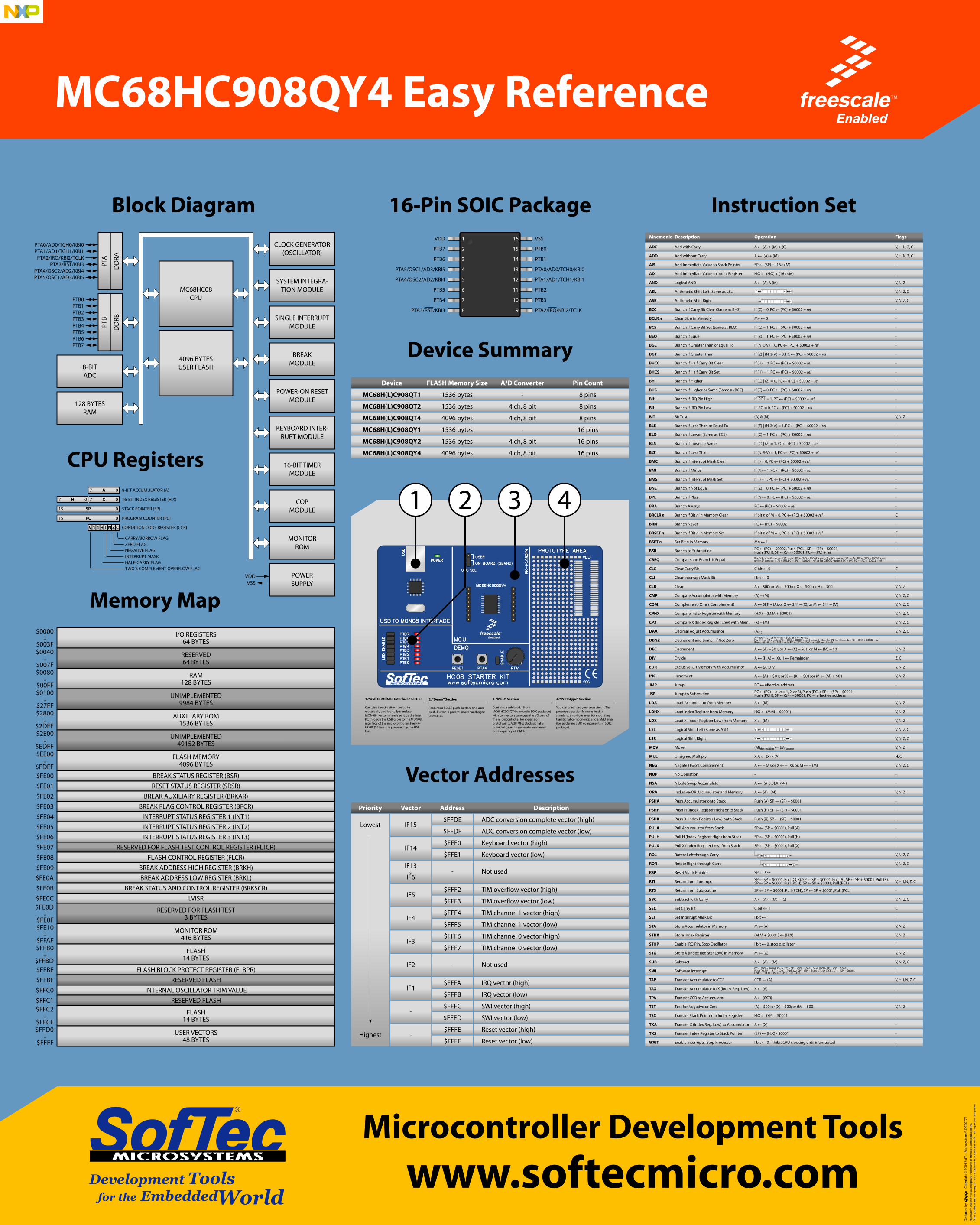
1. “USB to MON08 Interface” Section
Contains the circuitry needed to electrically and logically translate MON08-like commands sent by the host PC through the USB cable to the MON08 interface of the microcontroller. The PK-HC08QY4 board is powered by the USB bus.
2. “Demo” Section�
Features a RESET push-button, one user push-button, a potentiometer and eight user LEDs.
3. “MCU” Section
Contains a soldered, 16-pin MC68HC908QY4 device (in SOIC package) with connectors to access the I/O pins of the microcontroller for expansion prototyping. A 28 MHz clock signal is provided (used to generate an internal bus frequency of 7 MHz).
4. “Prototype” Section
You can wire here your own circuit. The prototype section features both a standard, thru-hole area (for mounting traditional components) and a SMD area (for soldering SMD components in SOIC package).
Instruction Set
TAX Transfer Accumulator to X (Index Reg. Low) X ← (A) -
Mnemonic Description Operation Flags
ADC Add with Carry A ← (A) + (M) + (C) V, H, N, Z, C
INC Increment A ← (A) + $01; or X ← (X) + $01; or M ← (M) + $01 V, N, Z
PSHA Push Accumulator onto Stack Push (A), SP ← (SP) − $0001 -
ORA Inclusive-OR Accumulator and Memory A ← (A) | (M) V, N, Z
NSA Nibble Swap Accumulator A ← (A[3:0]:A[7:4]) -
NOP No Operation - -
NEG Negate (Two’s Complement) A ← − (A); or X ← − (X); or: M ← − (M) V, N, Z, C
MUL Unsigned Multiply X:A ← (X) x (A) H, C
MOV Move (M)destination ← (M)source V, N, Z
LDHX Load Index Register from Memory H:X ← (M:M + $0001) V, N, Z
LDX Load X (Index Register Low) from Memory X ← (M) V, N, Z
LDA Load Accumulator from Memory A ← (M) V, N, Z
JMP Jump PC ← effective address -
EOR Exclusive-OR Memory with Accumulator A ← (A ⊕ M) V, N, Z
DIV Divide A ← (H:A) ÷ (X), H ← Remainder Z, C
DEC Decrement A ← (A) − $01; or X ← (X) − $01; or M ← (M) − $01 V, N, Z
DAA Decimal Adjust Accumulator (A)10 V, N, Z, C
CPX Compare X (Index Register Low) with Mem. (X) − (M) V, N, Z, C
CPHX Compare Index Register with Memory (H:X) − (M:M + $0001) V, N, Z, C
COM Complement (One’s Complement) A ← $FF − (A); or X ← $FF − (X); or M ← $FF − (M) V, N, Z, C
CMP Compare Accumulator with Memory (A) − (M) V, N, Z, C
CLR Clear A ← $00; or M ← $00; or X ← $00; or H ← $00 V, N, Z
CLI Clear Interrupt Mask Bit I bit ← 0 I
CLC Clear Carry Bit C bit ← 0 C
CBEQ Compare and Branch if Equal For DIR or IMM modes: if (A) = (M), PC ← (PC) + $0003 + rel; or for IX+ mode: if (A) = (M), PC ← (PC) + $0002 + rel;�or for SP1 mode: if (A) = (M), PC ← (PC) + $0004 + rel; or for CBEQX mode: if (X) = (M), PC ← (PC) + $0003 + rel -
BSR Branch to Subroutine PC ← (PC) + $0002, Push (PCL), SP ← (SP) − $0001,Push (PCH), SP ← (SP) - $0001, PC ← (PC) + rel -
BSET n Set Bit n in Memory Mn ← 1 -
BRSET n Branch if Bit n in Memory Set If bit n of M = 1, PC ← (PC) + $0003 + rel C
BRN Branch Never PC ← (PC) + $0002 -
BRCLR n Branch if Bit n in Memory Clear If bit n of M = 0, PC ← (PC) + $0003 + rel C
BRA Branch Always PC ← (PC) + $0002 + rel -
BPL Branch if Plus If (N) = 0, PC ← (PC) + $0002 + rel -
BNE Branch if Not Equal If (Z) = 0, PC ← (PC) + $0002 + rel -
BMS Branch if Interrupt Mask Set If (I) = 1, PC ← (PC) + $0002 + rel -
BMI Branch if Minus If (N) = 1, PC ← (PC) + $0002 + rel -
BMC Branch if Interrupt Mask Clear If (I) = 0, PC ← (PC) + $0002 + rel -
BLT Branch if Less Than If (N ⊕ V) = 1, PC ← (PC) + $0002 + rel -
BLS Branch if Lower or Same If (C) | (Z) = 1, PC ← (PC) + $0002 + rel -
BLO Branch if Lower (Same as BCS) If (C) = 1, PC ← (PC) + $0002 + rel -
BLE Branch if Less Than or Equal To If (Z) | (N ⊕ V) = 1, PC ← (PC) + $0002 + rel -
BIT Bit Test (A) & (M) V, N, Z
BHS Branch if Higher or Same (Same as BCC) If (C) = 0, PC ← (PC) + $0002 + rel -
BHI Branch if Higher If (C) | (Z) = 0, PC ← (PC) + $0002 + rel -
BHCS Branch if Half Carry Bit Set If (H) = 1, PC ← (PC) + $0002 + rel -
BHCC Branch if Half Carry Bit Clear If (H) = 0, PC ← (PC) + $0002 + rel -
BGT Branch if Greater Than If (Z) | (N ⊕ V) = 0, PC ← (PC) + $0002 + rel -
BGE Branch if Greater Than or Equal To If (N ⊕ V) = 0, PC ← (PC) + $0002 + rel -
BEQ Branch if Equal If (Z) = 1, PC ← (PC) + $0002 + rel -
BCS Branch if Carry Bit Set (Same as BLO) If (C) = 1, PC ← (PC) + $0002 + rel -
BCLR n Clear Bit n in Memory Mn ← 0 -
BCC Branch if Carry Bit Clear (Same as BHS) If (C) = 0, PC ← (PC) + $0002 + rel -
ADD Add without Carry A ← (A) + (M) V, H, N, Z, C
AIS Add Immediate Value to Stack Pointer SP ← (SP) + (16<<M) -
AIX Add Immediate Value to Index Register H:X ← (H:X) + (16<<M) -
AND Logical AND A ← (A) & (M) V, N, Z
ASL Arithmetic Shift Left (Same as LSL) V, N, Z, CC 7 0 0
ASR Arithmetic Shift Right V, N, Z, C7 0 C
LSL Logical Shift Left (Same as ASL) V, N, Z, CC 7 0 0
LSR Logical Shift Right V, N, Z, C0 7 0 C
PSHH Push H (Index Register High) onto Stack Push (H), SP ← (SP) − $0001 -
PULA Pull Accumulator from Stack SP ← (SP + $0001), Pull (A) -
PSHX Push X (Index Register Low) onto Stack Push (X), SP ← (SP) − $0001 -
PULH Pull H (Index Register High) from Stack SP ← (SP + $0001), Pull (H) -
PULX Pull X (Index Register Low) from Stack SP ← (SP + $0001), Pull (X) -
RSP Reset Stack Pointer SP ← $FF -
RTS Return from Subroutine SP ← SP + $0001, Pull (PCH), SP ← SP + $0001, Pull (PCL) -
SBC Subtract with Carry A ← (A) − (M) − (C) V, N, Z, C
SEC Set Carry Bit C bit ← 1 C
SEI Set Interrupt Mask Bit I bit ← 1 I
STA Store Accumulator in Memory M ← (A) V, N, Z
STHX Store Index Register (M:M + $0001) ← (H:X) V, N, Z
STOP Enable IRQ Pin, Stop Oscillator I bit ← 0, stop oscillator I
STX Store X (Index Register Low) in Memory M ← (X) V, N, Z
SUB Subtract A ← (A) − (M) V, N, Z, C
TAP Transfer Accumulator to CCR CCR ← (A) V, H, I, N, Z, C
TPA Transfer CCR to Accumulator A ← (CCR) -
TST Test for Negative or Zero (A) − $00; or (X) − $00; or (M) − $00 V, N, Z
TSX Transfer Stack Pointer to Index Register H:X ← (SP) + $0001 -
TXA Transfer X (Index Reg. Low) to Accumulator A ← (X) -
TXS Transfer Index Register to Stack Pointer (SP) ← (H:X) - $0001 -
WAIT Enable Interrupts, Stop Processor I bit ← 0, inhibit CPU clocking until interrupted I
BIL Branch if IRQ Pin Low If IRQ = 0, PC ← (PC) + $0002 + rel -
BIH Branch if IRQ Pin High If IRQ1 = 1, PC ← (PC) + $0002 + rel -
DBNZ Decrement and Branch if Not Zero -A ← (A) − $01; or M ← (M) − $01; or X ← (X) − $01For DIR or IX1 modes: PC ← (PC) + $0003 + rel if (result) ≠ 0; or for INH or IX modes: PC ← (PC) + $0002 + rel if (result) ≠ 0; or for SP1 mode: PC ← (PC) + $0004 + rel if (result) ≠ 0
JSR Jump to Subroutine -PC ← (PC) + n (n = 1, 2, or 3), Push (PCL), SP ← (SP) − $0001,�Push (PCH), SP ← (SP) − $0001, PC ← effective address
RTI Return from Interrupt V, H, I, N, Z, CSP ← SP + $0001, Pull (CCR), SP ← SP + $0001, Pull (A), SP ← SP + $0001, Pull (X), SP ← SP + $0001, Pull (PCH), SP ← SP + $0001, Pull (PCL)
SWI Software Interrupt IPC ← (PC) + $0001, Push (PCL), SP ← (SP) − $0001, Push (PCH), SP ← (SP) − $0001,�Push (X), SP ← (SP) − $0001, Push (A), SP ← (SP) − $0001, Push (CCR), SP ← (SP) − $0001,�I bit ← 1, PCH ← ($FFFC), PCL ← ($FFFD)
ROL Rotate Left through Carry V, N, Z, C0 CC 7 0
ROR Rotate Right through Carry V, N, Z, C7 0 C
Vector AddressesPriority Vector Address Description
$FFFF Reset vector (low)
Reset vector (high)$FFFE-
$FFFD SWI vector (low)
SWI vector (high)$FFFC-
$FFFB IRQ vector (low)
IRQ vector (high)$FFFAIF1
$FFF7 TIM channel 0 vector (low)
TIM channel 0 vector (high)$FFF6IF3
$FFF5 TIM channel 1 vector (low)
TIM channel 1 vector (high)$FFF4IF4
$FFF3 TIM overflow vector (low)
TIM overflow vector (high)$FFF2IF5
$FFDF ADC conversion complete vector (low)
ADC conversion complete vector (high)$FFDEIF15
IF13↓
IF6- Not used
$FFE1 Keyboard vector (low)
Keyboard vector (high)$FFE0IF14
IF2 - Not used
Lowest
Highest
MC68H(L)C908QT1 1536 bytes - 8 pins
MC68H(L)C908QT2 1536 bytes 4 ch, 8 bit 8 pins
MC68H(L)C908QT4 4096 bytes 4 ch, 8 bit 8 pins
MC68H(L)C908QY1 1536 bytes - 16 pins
MC68H(L)C908QY2 1536 bytes 4 ch, 8 bit 16 pins
MC68H(L)C908QY4 4096 bytes 4 ch, 8 bit 16 pins
Device FLASH Memory Size A/D Converter Pin Count
Device Summary

Microcontroller Development Tools
www.softecmicro.com Co
pyr
igh
t ©
200
4 So
fTec
Mic
rosy
stem
s®. D
C00
774
Des
ign
ed b
y
Free
scal
e™ a
nd
th
e Fr
eesc
ale
log
o a
re t
rad
emar
ks o
f Fre
esca
le S
emic
on
du
cto
r, In
c.O
ther
pro
du
cts
and
co
mp
any
nam
es a
re t
rad
emar
ks o
r tra
de
nam
es o
f th
eir r
esp
ecti
ve c
om
pan
ies.
PK-HC08QY4 Quickstart Tutorial
7 Run the Example
Choose Run > Start/Continue from the main menu. The program will be executed in real-time. By rotating the potentiometer on the board, you affect the results of the A/D conversion. The binary value of each conversion is displayed on the LEDs.
hcPX@starter@kit
pkMhcPXqyT
pkMhcPXqyT
pkMhcPXqyT
vddvddvdd
ptaQptaQptaQptaTptaTptaTresetresetreset
usbusbusbtototo monPXmonPXmonPX
mcumcumcu
enable
enable
enable
demo@@@@demo@@@@demo@@@@
prototype@areaprototype@areaprototype@area
interfaceinterfaceinterface
usb
usb
usb
powerpowerpower
led@enable
led@enable
led@enable
ptbWptbWptbWptbVptbVptbVptbUptbUptbUptbTptbTptbTptbSptbSptbSptbRptbRptbRptbQptbQptbQptbPptbPptbP
useruseruser
on@board@HRXmhÂIon@board@HRXmhÂIon@board@HRXmhÂI
oscoscosc selselsel
mcVXhcYPXqyTmcVXhcYPXqyTmcVXhcYPXqyT
2 Install theInstrument Software
SofTec Microsystems Additional Components include the PK-HC08QY4 USB driver, the PK-HC08QY4 software plug-in for CodeWarrior HC(S)08, SofTec Microsystems DataBlaze programming utility, examples and documentation in PDF format.
To install the SofTec Microsystems Additional Components, insert the SofTec Microsystems
“System Software” CD-ROM into your computer’s CD-ROM drive. A startup
window will automatically appear. Choose “Install Instrument
Software” from the main menu. Click on the “PK-HC08 Series Additional Components” option. Follow the on-screen instructions.
3 Connect the Boardto the PC
Connect PK-HC08QY4 to a free USB port on your PC. The green “POWER” LED on the instrument will turn on.
hcPX@starter@kit
pkMhcPXqyT
pkMhcPXqyT
pkMhcPXqyT
vddvddvdd
ptaQptaQptaQptaTptaTptaTresetresetreset
usbusbusbtototo monPXmonPXmonPX
mcumcumcu
enable
enable
enable
demo@@@@demo@@@@demo@@@@
prototype@areaprototype@areaprototype@area
interfaceinterfaceinterface
usb
usb
usb
powerpowerpower
led@enable
led@enable
led@enable
ptbWptbWptbWptbVptbVptbVptbUptbUptbUptbTptbTptbTptbSptbSptbSptbRptbRptbRptbQptbQptbQptbPptbPptbP
useruseruser
on@board@HRXmhÂIon@board@HRXmhÂIon@board@HRXmhÂI
oscoscosc selselsel
mcVXhcYPXqyTmcVXhcYPXqyTmcVXhcYPXqyT
8Congratulations!
You have successfully completed this tutorial! You can now continue to experiment with the CodeWarrior user interface and discover its potentialities (step commands, breakpoints, watch windows, etc.) on your own.
Please also read carefully all of the PK-HC08QY4 documentation.
For the latest software releases,new products, new supported devices,
discussion forums and FAQs,log on to
http://www.softecmicro.com/
4 Found NewHardware Wizard
The first time PK-HC08QY4 is connected to the PC, Windows recognizes the instrument and starts the “Found New Hardware Wizard” procedure, asking you to specify the drivers to use for the instrument.
The procedure is slightly different on each version of Windows. On Windows XP, select the “Install the software automatically” option and click on the “Next” button.
Be sure not to specify any drive or optional location where to look for the driver, since it has already been installed on your hard disk by the PK-HC08 Series Additional Components setup.
Note: both Windows 2000 and Windows XP may issue a warning during the “Found New Hardware Wizard” procedure. This warning is related to the fact that the USB driver used by PK-HC08QY4 is not digitally signed by Microsoft, and Windows considers it to be potentially malfunctioning or dangerous for the system. However, you can safely ignore the warning, since every kind of compatibility/security test has been carried out by SofTec Microsystems.
5 Run CodeWarrior andOpen the Example
Start the CodeWarrior IDE by selecting Start > Programs > Metrowerks CodeWarrior > CW08 > CodeWarrior IDE. The CodeWarrior IDE will open.
Choose File > Open from the main menu.
Select the “ADC.mcp” workspace file that is located in the�“[Programs Folder]\Metrowerks\CodeWarrior CW08\�(CodeWarrior_Examples)\HC08\SofTec Microsystems\�PK-HC08QY4\C\ADC” folder.
Click “Open”.
1 Install CodeWarriorfor HC(S)08
PK-HC08QY4 comes with a free version of CodeWarrior Development Studio for HC(S)08 Microcontrollers, Special Edition.
CodeWarrior Development Studio for HC(S)08 Microcontrollers, Special Edition, includes the CodeWarrior integrated development
environment (IDE); 4 KB code-size limited C compiler and C source-level debugger; macro assembler
and Assembly-level debugger. The Special Edition allows you to evaluate
CodeWarrior Development Studio for HC(S)08 Microcontrollers at no cost.
To install the CodeWarrior IDE, insert the CodeWarrior CD-ROM into your computer’s CD-ROM drive. A startup window will automatically appear. Follow the on-screen instructions.
�Note: PK-HC08QY4 requires that a
CodeWarrior version equal to or greater than 3.0 is present on your
system. If you have an earlier version on your system, you must uninstall it and
install the new CodeWarrior version which comes with PK-HC08QY4. If you purchased an
earlier CodeWarrior version, we advise you to contact Metrowerks to have your license extended to
the new version.
6 Start a DebuggingSession
Choose Project > Debug from the main menu. This will generate an executable file and will download it to the board.
A new debugger environment will open.
hcPX@starter@kit
pkMhcPXqyT
pkMhcPXqyT
pkMhcPXqyT
vddvddvdd
ptaQptaQptaQptaTptaTptaTresetresetreset
usbusbusbtototo monPXmonPXmonPX
mcumcumcu
enable
enable
enable
demo@@@@demo@@@@demo@@@@
prototype@areaprototype@areaprototype@area
interfaceinterfaceinterface
usb
usb
usb
powerpowerpower
led@enable
led@enable
led@enable
ptbWptbWptbWptbVptbVptbVptbUptbUptbUptbTptbTptbTptbSptbSptbSptbRptbRptbRptbQptbQptbQptbPptbPptbP
useruseruser
on@board@HRXmhÂIon@board@HRXmhÂIon@board@HRXmhÂI
oscoscosc selselsel
mcVXhcYPXqyTmcVXhcYPXqyTmcVXhcYPXqyT
1 432
1. “USB to MON08 Interface” Section
Contains the circuitry needed to electrically and logically translate MON08-like commands sent by the host PC through the USB cable to the MON08 interface of the microcontroller. The PK-HC08QY4 board is powered by the USB bus.
2. “Demo” Section�
Features a RESET push-button, one user push-button, a potentiometer and eight user LEDs.
3. “MCU” Section
Contains a soldered, 16-pin MC68HC908QY4 device (in SOIC package) with connectors to access the I/O pins of the microcontroller for expansion prototyping. A 28 MHz clock signal is provided (used to generate an internal bus frequency of 7 MHz).
4. “Prototype” Section
You can wire here your own circuit. The prototype section features both a standard, thru-hole area (for mounting traditional components) and a SMD area (for soldering SMD components in SOIC package).