mcc255-14io1
TRANSCRIPT
© 2000 IXYS All rights reserved 1 - 4
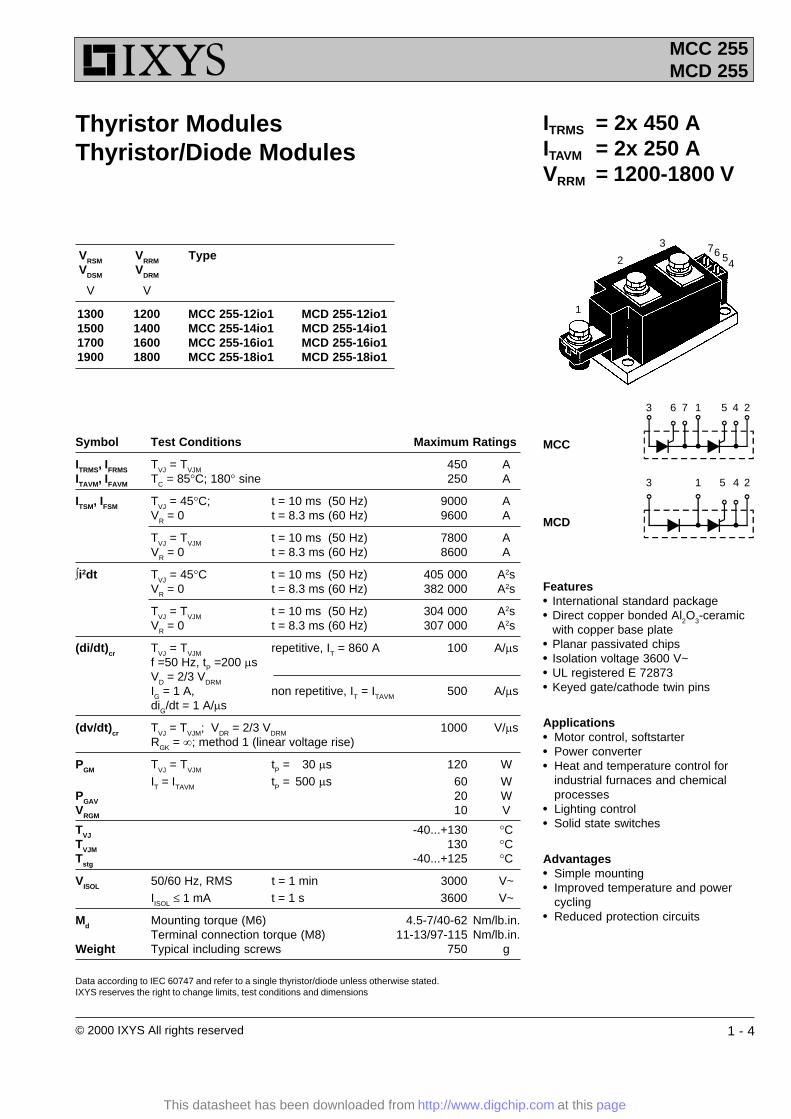
VRSM VRRM TypeVDSM VDRM
V V
1300 1200 MCC 255-12io1 MCD 255-12io11500 1400 MCC 255-14io1 MCD 255-14io11700 1600 MCC 255-16io1 MCD 255-16io11900 1800 MCC 255-18io1 MCD 255-18io1
Symbol Test Conditions Maximum Ratings
ITRMS, IFRMS TVJ = TVJM 450 AITAVM, IFAVM TC = 85�C; 180� sine 250 A
ITSM, IFSM TVJ = 45�C; t = 10 ms (50 Hz) 9000 AVR = 0 t = 8.3 ms (60 Hz) 9600 A
TVJ = TVJM t = 10 ms (50 Hz) 7800 AVR = 0 t = 8.3 ms (60 Hz) 8600 A
�i2dt TVJ = 45�C t = 10 ms (50 Hz) 405 000 A2sVR = 0 t = 8.3 ms (60 Hz) 382 000 A2s
TVJ = TVJM t = 10 ms (50 Hz) 304 000 A2sVR = 0 t = 8.3 ms (60 Hz) 307 000 A2s
(di/dt)cr TVJ = TVJM repetitive, IT = 860 A 100 A/�sf =50 Hz, tP =200 �sVD = 2/3 VDRM
IG = 1 A, non repetitive, IT = ITAVM 500 A/�sdiG/dt = 1 A/�s
(dv/dt)cr TVJ = TVJM; VDR = 2/3 VDRM 1000 V/�sRGK = �; method 1 (linear voltage rise)
PGM TVJ = TVJM tP = 30 �s 120 WIT = ITAVM tP = 500 �s 60 W
PGAV 20 WVRGM 10 V
TVJ -40...+130 �CTVJM 130 �CTstg -40...+125 �C
VISOL 50/60 Hz, RMS t = 1 min 3000 V~IISOL � 1 mA t = 1 s 3600 V~
Md Mounting torque (M6) 4.5-7/40-62 Nm/lb.in.Terminal connection torque (M8) 11-13/97-115 Nm/lb.in.
Weight Typical including screws 750 g
Features● International standard package● Direct copper bonded Al2O3-ceramic
with copper base plate● Planar passivated chips● Isolation voltage 3600 V~● UL registered E 72873● Keyed gate/cathode twin pins
Applications● Motor control, softstarter● Power converter● Heat and temperature control for
industrial furnaces and chemicalprocesses
● Lighting control● Solid state switches
Advantages● Simple mounting● Improved temperature and power
cycling● Reduced protection circuits
ITRMS = 2x 450 AITAVM = 2x 250 AVRRM = 1200-1800 V
Data according to IEC 60747 and refer to a single thyristor/diode unless otherwise stated.IXYS reserves the right to change limits, test conditions and dimensions
MCC 255MCD 255
Thyristor ModulesThyristor/Diode Modules
1
2
3 76 54
MCD
MCC
3 6 7 1 5 4 2
3 1 5 4 2
This datasheet has been downloaded from http://www.digchip.com at this page
© 2000 IXYS All rights reserved 2 - 4
MCC 255MCD 255
Symbol Test Conditions Characteristic Values
IRRM, IDRM TVJ = TVJM; VR = VRRM; VD = VDRM 40 mA
VT, VF IT, IF = 600 A; TVJ = 25�C 1.36 V
VT0 For power-loss calculations only (TVJ = 130�C) 0.8 VrT 0.68 m�
VGT VD = 6 V; TVJ = 25�C 2 VTVJ = -40�C 3 V
IGT VD = 6 V; TVJ = 25�C 150 mATVJ = -40�C 220 mA
VGD TVJ = TVJM; VD = 2/3 VDRM 0.25 VIGD TVJ = TVJM; VD = 2/3 VDRM 10 mA
IL TVJ = 25�C; tP = 30 �s; VD = 6 V 200 mAIG = 0.45 A; diG/dt = 0.45 A/�s
IH TVJ = 25�C; VD = 6 V; RGK = � 150 mA
tgd TVJ = 25�C; VD = 1/2 VDRM 2 �sIG = 1 A; diG/dt = 1 A/�s
tq TVJ = TVJM; IT = 300 A, tP = 200 �s; -di/dt = 10 A/�s typ. 200 �sVR = 100 V; dv/dt = 50 V/�s; VD = 2/3 VDRM
QS TVJ = 125�C; IT, IF = 300 A; -di/dt = 50 A/�s 760 �CIRM 275 A
RthJC per thyristor (diode); DC current 0.140 K/Wper module other values 0.07 K/W
RthJK per thyristor (diode); DC current see Fig. 8/9 0.18 K/Wper module 0.09 K/W
dS Creeping distance on surface 12.7 mmdA Creepage distance in air 9.6 mma Maximum allowable acceleration 50 m/s2
Optional accessories for modulesKeyed Gate/Cathode twin plugs with wire length = 350 mm, gate = yellow, cathode = redType ZY 180 L (L = Left for pin pair 4/5) UL 758, style 1385,Type ZY 180 R (R = Right for pin pair 6/7) CSA class 5851, guide 460-1-1
Dimensions in mm (1 mm = 0.0394")
MCC 255 MCD 255
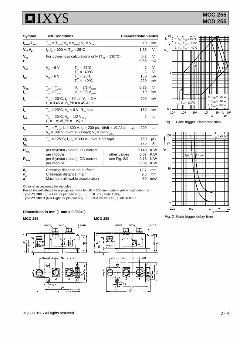
Fig. 1 Gate trigger characteristics
Fig. 2 Gate trigger delay time
0.01 0.1 1 10
1
10
100
10-3 10-2 10-1 100 101 1020.1
1
10
IG
VG
A
AIG
1: IGT, TVJ = 140°C
2: IGT, TVJ = 25°C
3: IGT, TVJ = -40°C
µs
tgd
V
4: PGM = 20 W
5: PGM = 60 W
6: PGM = 120 WIGD, TVJ = 140°C
4
2
15
6
Limittyp.
TVJ = 25°C
3
0.01 0.1 1 10
1
10
100
10-3 10-2 10-1 100 101 1020.1
1
10
IG
VG
A
AIG
1: IGT, TVJ = 130°C
2: IGT, TVJ = 25°C
3: IGT, TVJ = -40°C
µs
tgd
V
4: PGM = 20 W
5: PGM = 60 W
6: PGM = 120 WIGD, TVJ = 130°C
4
2
15
6
Limittyp.
TVJ = 25°C
3
M8x20 M8x20
© 2000 IXYS All rights reserved 3 - 4
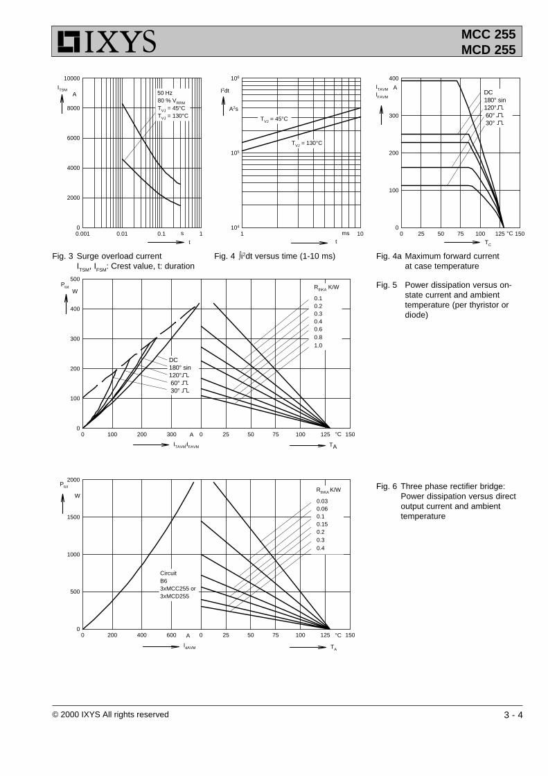
I2dt
ITAVM/IFAVM
IdAVM
Ptot
W
TA
TA
TC
st
ms
t
0.001 0.01 0.1 10
2000
4000
6000
8000
10000
1 10104
105
106
A2s
0 25 50 75 100 125 1500
100
200
300
400
ITSMA
A
°C
ITAVM
IFAVM
0 25 50 75 100 125 1500 100 200 3000
100
200
300
400
500
WPtot
A °C
RthKA K/W
0 25 50 75 100 125 1500 200 400 6000
500
1000
1500
2000
°C
0.10.20.30.40.60.81.0
80 % VRRM
TVJ = 45°C
50 Hz
TVJ = 130°C TVJ = 45°C
TVJ = 130°C
A
RthKA K/W
0.030.060.10.150.20.30.4
CircuitB6
3xMCD2553xMCC255 or
180° sin120° 60° 30°
DC
180° sin120° 60° 30°
DC
MCC 255MCD 255
Fig. 3 Surge overload currentITSM, IFSM: Crest value, t: duration
Fig. 4 �i2dt versus time (1-10 ms) Fig. 4a Maximum forward currentat case temperature
Fig. 5 Power dissipation versus on-state current and ambienttemperature (per thyristor ordiode)
Fig. 6 Three phase rectifier bridge:Power dissipation versus directoutput current and ambienttemperature
© 2000 IXYS All rights reserved 4 - 4
MCC 255MCD 255
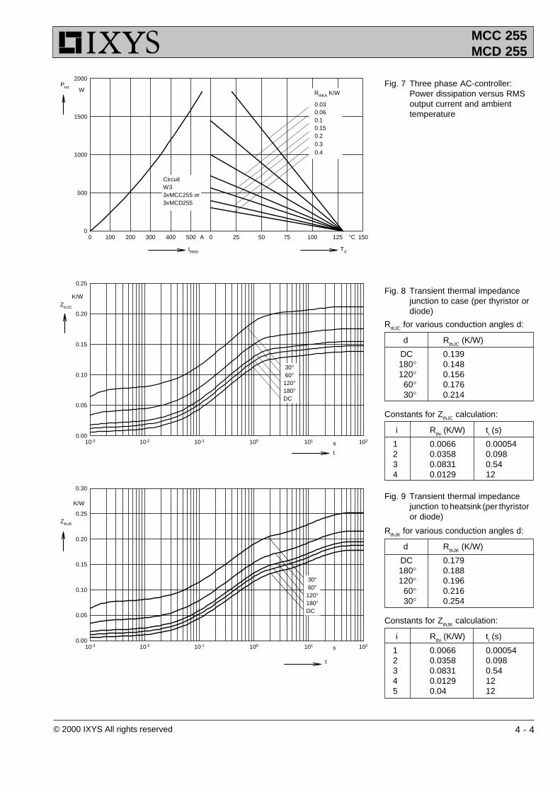
Fig. 7 Three phase AC-controller:Power dissipation versus RMSoutput current and ambienttemperature
Fig. 8 Transient thermal impedancejunction to case (per thyristor ordiode)
RthJC for various conduction angles d:
d RthJC (K/W)
DC 0.139180� 0.148120� 0.156
60� 0.17630� 0.214
Constants for ZthJC calculation:
i Rthi (K/W) ti (s)
1 0.0066 0.000542 0.0358 0.0983 0.0831 0.544 0.0129 12
Fig. 9 Transient thermal impedancejunction to heatsink (per thyristoror diode)
RthJK for various conduction angles d:
d RthJK (K/W)
DC 0.179180� 0.188120� 0.196
60� 0.21630� 0.254
Constants for ZthJK calculation:
i Rthi (K/W) ti (s)
1 0.0066 0.000542 0.0358 0.0983 0.0831 0.544 0.0129 125 0.04 12
s
t
ZthJK
s
t
10-3 10-2 10-1 100 101 1020.00
0.05
0.10
0.15
0.20
0.25
0.30
K/W
ZthJC
K/W
IRMS
WPtot
0 25 50 75 100 125 1500 100 200 300 400 5000
500
1000
1500
2000
A
TA
°C
10-3 10-2 10-1 100 101 1020.00
0.05
0.10
0.15
0.20
0.25
DC180°120° 60° 30°
DC180°120° 60° 30°
RthKA K/W
0.030.060.10.150.20.30.4
CircuitW3
3xMCD2553xMCC255 or