measurements and simulation of conductor-related loss of
TRANSCRIPT

Scholars Mine Scholars Mine
Masters Theses Student Theses and Dissertations
Spring 2016
Measurements and simulation of conductor-related loss of PCB Measurements and simulation of conductor-related loss of PCB
transmission lines transmission lines
Oleg Kashurkin
Follow this and additional works at httpsscholarsminemstedumasters_theses
Part of the Electrical and Computer Engineering Commons
Department Department
Recommended Citation Recommended Citation Kashurkin Oleg Measurements and simulation of conductor-related loss of PCB transmission lines (2016) Masters Theses 7508 httpsscholarsminemstedumasters_theses7508
This thesis is brought to you by Scholars Mine a service of the Missouri SampT Library and Learning Resources This work is protected by U S Copyright Law Unauthorized use including reproduction for redistribution requires the permission of the copyright holder For more information please contact scholarsminemstedu
MEASUREMENTS AND SIMULATION OF CONDUCTOR-
RELATED LOSS OF PCB TRANSMISSION LINES
by
OLEG KASHURKIN
A THESIS
Presented to the Faculty of the Graduate School of the
MISSOURI UNIVERSITY OF SCIENCE AND TECHNOLOGY
In Partial Fulfillment of the Requirements for the Degree
MASTER OF SCIENCE IN ELECTRICAL ENGINEERING
2016
Approved by
Victor Khilkevich Advisor
David Pommerenke
Jun Fan
2016
Oleg Kashurkin
All Rights Reserved
iii
ABSTRACT
With continuously increasing data rates Signal Integrity (SI) problems become
more and more challenging One of the main issues in high-speed data transfer is the
frequency-dependent loss of transmission lines This thesis is dedicated to conductor-
related loss mechanisms in printed circuit board (PCB) transmission lines
This thesis provides the experimental investigation of conductor properties used
for fabrication of PCBs Particularly the resistivity and conductivity along with the
temperature coefficients of eleven copper types is measured and reported A four probe
measurement technique is used Results were verified by two independent measurements
and show discrepancy of less than 05
Another major conductor-related loss mechanism is the attenuation of the
electromagnetic waves due to the surface roughness of PCB conductors There are
several models attempting to take into account the roughness effect However none of
them are able to explain or predict the transmission line behavior with high accuracy
Particularly the experimental observations show that the slope of S21 curves increases
with frequency which cannot be modelled by the existing model To better understand
the physics associated with the loss due to the surface roughness of conductors and be
able to predict the behavior of transmission lines in the future a full wave model of
surface roughness was developed The detailed methodology for 3D roughness
generation is provided
iv
ACKNOWLEDGMENTS
I would like to express my sincere gratitude and deep appreciation to my advisor
Dr Victor Khilkevich for guidance toward my academic path ideas and help with
experiment conducting technique I am very thankful him for introduction to real world
electrical engineering revel modern and challenge problems of high-speed design and
EMC I express my sincere gratitude to Dr Marina Y Koledintseva for her constant
support and inspiration for work I thank Dr James L Drewniak for his mentoring and
guidance in my career and manage project I was involved in as part of the EMC
Laboratory and for giving me this opportunity to be a member of EMC lab I am very
grateful to Mr Scott Hinaga from Cisco Systems Inc for his encouragement attention to
new ideas and techniques and exceptional help throughout my project work
I want to show my deep gratitude to all professors of the EMC Laboratory for
giving me priceless knowledge during course work and showing faith in me as a graduate
student I greatly appreciate classes of Dr David Pommerenke and Dr Jun Fan which
straightened my understanding of Electromagnetics and Wave propagation Theory I
thank all my fellow laboratory students who gave me advice and helped me to go
through any problems I encountered
Finally I would like to thank my beloved family especially my wife Tatiana
Platova for her endless and unconditional love support and encouragement through all
my education and life
This thesis is based upon work supported partially by the National Science
Foundation under Grant No IIP-1440110
v
TABLE OF CONTENTS
Page
ABSTRACT iii
ACKNOWLEDGMENTS iv
LIST OF ILLUSTRATIONS vii
LIST OF TABLES ix
NOMENCLATURE x
SECTION
1 INTRODUCTION 1
11 CONDUCTOR ndash RELATED LOSS IN TRANSMISSION LINE 2
2 MEASUREMENT OF COPPER RESISTIVITY 6
21 BACKGROUND 6
211 Four-Probe Technique 8
212 Setup 9
213 DUT Description 12
214 Uncertainty Estimation 13
215 Results and Discussion 15
22SUMMARY 21
3 SURFACE ROUGHNESS MODELING 22
31 EXPERIMENTAL INVESTIGATION OF SURFACE ROUGHNESS
EFFECTS 22
311 Measurement Results and Observations 23
312 Motivation and Objective 27
32 EXISTING MODELS FOR SURFACE ROUGHNESS 27
321 Hammerstad Model 27
322 Hemispherical Model 30
323 Snowball Model 32
324 Small Pertrubation Method 34
325 Scalar Wave Modeling 36
326 Limitations of Existing Models 36
vi
33 3D MODEL FOR SURFACE ROUGHNESS 37
331 Extraction of Roughness Parameters 37
332 Generation of the 3D Surface 40
333 Surface Roughness Modeling in CST Microwave Studio 46
334 Results and Discussion 48
4 CONCLUSION 54
BIBLIOGRAPHY 55
VITA 60
vii
LIST OF ILLUSTRATIONS
Figure Page
11 Modeled transmission coefficients of stripline at 25 and 125 4
12 Optical microscopic images of roughness From left to right STD (standard)
VLP (very low profile) HVLP (hyper very low profile) 5
13 Hall Hemispherical model used in ADS [5] (a) GMS model developed in
Simberian Inc [11] (b) 5
21 Schematic of Four - Point Probe Technique 8
22 Pogo pin (left) Customized probes for resistivity measurements (right) 9
23 Setup schematic for resistance measurements 10
24 Setup for resistance measurements (a) window for probes landing (b) two
thermocouples placed on the DUT (c)11
25 Top layer of tested coupon 12
26 The cross section of the tested trace 13
27 Allesi C4S 4-point probe 16
28 Conductivity over temperature for all tested copper types 19
29 Resistivity over temperature for all tested copper types 19
210 Resistivity vs temperature 20
31 Picture of the test vehicle 22
32 Drawing of SMA connector 23
33 |S21| per inch for the entire PCBs set 24
34 Nonlinear behavior of the insertion loss due to the surface roughness [29] 25
35 Measured of the real and imaginary components of Roger 5880 [33] 26
36 DK DF of bismaleimide triazine (BT) [47] 26
37 Hammersted model for roughness modeling 28
38 Roughness correction factor based on Hammersted model 29
39 Measured and corrected according to Hammersted insertion loss [5] 29
310 Hemispherical model for roughness modeling 31
311 Roughness correction factor based on Hemispherical model 31
312 Measured and corrected according to Hall insertion loss [5] 32
313 Snowballs model for roughness modeling [36] 32
viii
314 Roughness correction factor based on Snowballs model 33
315 Measured and corrected according to Snowball model insertion loss [5] 34
316 Roughness correction factor based on SPM2 35
317 Measured and modeled according to SPM2 [39] 35
318 Roughness correction factor calculated by SWM vs SPM2 [43] 36
319 Prepared sample for cross section analysis (a) microscopic pictures of stripline
(b) close-up picture of the trace (c) 38
320 Binary image of the cross-section for VLP38
321 Extracted roughness profile of VLP foil (oxide side) 39
322 Autocorrelation function of the VLP foil roughness profile Correlation length
is indicated by the marker 39
323 Histogram of VLP foil 40
324 Frequency response of a 1D FIR prototype filter 41
325 Frequency responses for Wn=01 (right) and Wn=08 (left) N=4 in both cases 42
326 Surface roughness profile measured by a profilometer [5] (left) and generated
(right) 43
327 Autocorrelation function of δ-correlated sequence 43
328 Measured and generated profiles of the surface roughness with dx=lACR
(13μm) 44
329 Measured and generated profiles of the surface roughness with dx=l11986011986211987710
(013μm) 45
330 Stripline structure to model the surface roughness 47
331 Boundary condition and planes of symmetry used for simulation Blue ndash
magnetic walls green ndash electric walls 47
332 Zoom of the end of the trace with surface roughness 47
333 Five different realization of surface with same parameters 49
334 Modeled (a) and measured (b) insertion loss for different roughness magnitude
up to 10 GHz 49
335 Modeled insertion loss for different roughness magnitude up to 50GHz 50
336 Modeled return loss for different roughness magnitude up to 50GHz 51
337 Absorption losses for striplines different roughness magnitude up to 50GHz 51
338 Modeled insertion loss for different length of stripline 52
339 Modeled return loss for different length of stripline 52
340 Absorption losses for striplines of different length up to 50GHz 53
ix
LIST OF TABLES
Table Page
21 Values for the electrical resistivity and temperature coefficients of annealed
copper 7
22 Thickness width and area of traces 14
23 Comparison of conductivity obtained by two methods (3 copper types are
shown) 16
24 Conductivity at room temperature 50 C and 100 C 17
25 Resistivity at room temperature 50 C and 100 C 18
26 Temperature coefficients for tested copper foils 20
31 Roughness parameters for three tested foil types [47] 23
32 Difference in loss for different trace width at 15GHz 24
33 Filter parameters for two discretization steps 44
34 Tetrahedrons and time required for different discretization step 48
x
NOMENCLATURE
Symbol Description
E Electric field vector
E0 Electromagnetic wave amplitude
ω Angular frequency
119891 Frequency
k Wave number
120574 Propagation constant
120572 Total attenuation constant
120573 Phase constant
120572119888 Conductor loss
120572119889 Dielectric loss
120575 Skin depth
120590 Conductivity of metal
120583 Absolute permeability
ε Absolute permittivity
120588 Resistivity
ρ0 Resistivity at reference temperature
T0 Reference temperature
αT Temperature coefficient
ℎ119903119898119904 ldquoroot-mean-squaredrdquo (RMS) value of surface roughness magnitude
119869 Current density
xi
I Current
A Cross section area of the trace
119909120583 Mean value of sequence
R Resistance
S Standard deviation
∆119906 Standard uncertainty
∆120588 Uncertainty in resistivity
119870119904 Power loss coefficient
Atile Title area
119860119887119886119904119890 Base area of the hemispheres
W(kx ky) Power spectral frequency function
119897ACR Correlation length
Wn Normalized cut-off frequency
G Gain of the FIR filter
1 INTRODUCTION
The complexity of design and rapidly increasing data rate in high-speed digital
electronics makes the signal integrity performance hard to maintain As the data rate
increases the loss in transmission lines becomes the main issue for signals with clock
higher than 1GHz [1] As a signal propagates along a transmission line the frequency
dependent loss causes the signal degradation as the high-frequency part of the spectrum
experiences higher attenuation A transmission line with high loss causes more signal
distortion and limits the speed of the transmitted data This makes it important to
determine the high-frequency loss behavior in PCBs at the design stage
There are several mechanisms of loss in transmission lines but the primary ones
are conductor loss dielectric loss and loss due to the surface roughness of the traces [1]
Models of transmission lines need to take into account all three physical loss
mechanisms The conductor and dielectric loss are relatively well studied and good
models for them exist [2] In order to use these models the parameters of materials need
to be determined by measurement The conductor loss is equally important as the
dielectric loss but it is typical to use nominal value for the resistivity of copper to model
PCB transmission lines [1 2] In this work a practical and easy-to-implement method for
the conductor loss measurement (including temperature dependency) is presented The
obtained results indicate that the actual resistivity of copper used to create PCB
interconnects is noticeably lower than the nominal value and needs to be measured in
order to improve the accuracy of the transmission line modeling
Another very important factor determining the loss of PCB transmission lines is
the surface roughness of copper layers [3][4] Despite its importance there is still no
satisfactory understanding of physical mechanisms responsible for the roughness-related
attenuation and existing models do not provide enough accuracy in many cases as will be
shown further In this work a new full-wave model of conductor surface roughness is
proposed that can be used to investigate physical effect associated with conductor
surface roughness
2
11 CONDUCTOR ndash RELATED LOSS IN TRANSMISSION LINE
An electromagnetic wave propagating inside any real physical medium
experiences attenuation or in other words such medium has loss The attenuation is
characterized by attenuation constant and is related to the material properties of the
particular medium The electric field of the x-polarized TEM plane wave propagating
along z coordinate is [6]
119812(119911) = 1198640119890minus120574z119890ωt119857 (1)
where 1198640 is the wave amplitude ω is the angular frequency x is the unit vector in x
direction and 120574 is a propagation constant given as
120574 = 120572 + 119895120573 (2)
where 120572 is attenuation constant and 120573 is the phase constant which determines the wave
speed in medium it propagates in Usually waveguide structures consist of conductor and
dielectric both contributing to the attenuation constant In such structures the propagating
electromagnetic wave is attenuated mainly due to the conductor and dielectric loss but
other factors such as conductor surface roughness are also relevant [5] For low-loss
transmission lines it is possible to separate the total attenuation into a conductor loss and
dielectric loss components [1] [2]
120572 asymp 120572119888 + 120572119889 (3)
Conductor loss 120572119888 is related to the skin depth 120572119888 prop 1120575 which is defined as the
depth where the amplitude of the field vectors decays 119890 times In good conductor the skin
depth is [1][3]
120575 asymp radic1
119891120590120587120583 (4)
3
where f is the frequency σ is the electrical conductivity and micro is the permeability of the
conductor The electrical conductivity is reciprocal to the electrical resistivity 120590 = 1120588
and measures a materials ability to conduct an electric current
The skin effect describes the tendency of alternating current (AC) to flow near the
conductor surface The direct current (DC) distributes uniformly within the entire cross
section of the conductor and the resistive loss in this case relates to the cross-section area
of the conductor and metal conductivity but as the frequency increases the current begins
to flow in a thin layer beneath the surface of conductor approximately equal to the skin
depth The skin effect shrinks the effective cross-section of the conductor increasing the
resistance proportionally to radic119891 Therefore the conductor loss depends on the material
properties geometry of the conductor and is frequency-dependent
At the same time the resistivity of metals is temperature-dependent If the
temperature T changes within several hundred of K the temperature dependence of
electrical resistance is can be approximated by a linear function [7]
120588(119879) asymp 1205880[1 + 120572119879(119879 minus 1198790)] (5)
where 1205880 is the resistivity (in Ωm) at the reference temperature T0 and αT is the
temperature coefficient of resistivity (in minus1 or Kminus1)
Due to high current consumption the operating temperature of modern equipment
is typically considerably higher than room temperature [8] The temperature is high
enough to noticeably increase of resistivity and therefore the attenuation of the
transmission line The example of the increased loss due to temperature is shown on
Figure 11 Simulations were done for a 5000 mil long stripline structure having 3 mil
trace width and 91 mil thickness of the bulk dielectric Dielectric has the dielectric
constant (DK) of 4 and dissipation factor (DF) equal to 0008 (medium-loss dielectric)
Applying Eq4 and using 1205880 = 1724 ∙ 10minus8 Ωm (nominal value for pure copper)
120572119879 = 000393 1 1198790 = 25 the resistivity at 119879 = 25 and 119879 = 125 is
calculated After that the transmission coefficient of the line is calculated using the model
in Advanced Design System [45] The resulting coefficients are shown in Figure 11 As
4
can be seen increasing the temperature by 100 C leads to 1 dB difference at 50 GHz and
cannot be neglected in some cases
Figure11 Modeled transmission coefficients of stripline at 25 and 125
The purpose of Chapter 2 of the thesis is to study the temperature dependency of
resistance for different copper types used in PCB design
As was said above the conductor surface roughness is an important factor
affecting the performance of high-speed transmission lines Real PCB traces are not
smooth and the surface quality depends on technological process used during the PCB
fabrication [9] Also copper traces in transmission lines are intentionally made rough to
promote adhesion to the dielectric Typically ldquoroot-mean-squaredrdquo (RMS) value of
roughness is calculated as [10]
ℎ119903119898119904 = radicE [(119883 minus 119909120583)2
] (6)
where X is the profile function 119909120583 is the mean value of X and E denotes as expected
value operator
There are other parameters of surface roughness that can be found in literature
For example Rz referred to as ten point height is the average absolute value of the five
highest peaks and the five lowest valleys The ℎ119903119898119904 (or Rq in literature) typically is 025-
07μm for hyper very low profile (HVLP) foils 03-10μm for very low profile (VLP)
0 10 20 30 40 50-16
-14
-12
-10
-8
-6
-4
-2
0
Frequency (GHz)
|S21| d
B
T=125 C
T=25 C
5
foils and 10-20μm for standard profile (STD) foils [1 9 10 48] The examples of
several foil type profiles are presented in Figure 12
Figure 12 Optical microscopic images of roughness From left to right STD (standard)
VLP (very low profile) HVLP (hyper very low profile)
At frequencies starting from approximately 2GHz the skin depth becomes
comparable to the RMS height of the surface roughness impacting the flow of the current
considerably
Modern commercial software tools have models for conductor surface roughness
in transmission lines however all of them provide insufficient accuracy (in-depth review
of models is presented in Section 3) Examples are presented in Figure 13
Figure13 Hall Hemispherical model used in ADS [5] (a) GMS model developed in
Simberian Inc [11] (b)
In order to improve our understanding of the physical processes in striplines with
rough conductors a full-wave model is proposed in Section 3 It might be used in the
future as the basis of a truly physics-based roughness model
a b
6
2 MEASUREMENT OF COPPER RESISTIVITY
Pure copper has relatively low electrical resistivity among commercially useful
metals On the other hand the resistivity of different copper types used for PCB
fabrication might vary [12]What is worse is that thermal processing of copper (like
annealing) affects the resistivity profoundly [13] Because of this it becomes impossible
in many cases to predict the actual resistivity of conductors in PCBs
Resistivity is temperature dependent if the temperature increases resistivity
increases as well This chapter will outline the methodology for temperature dependence
measurements of the resistivity A quick explanation of four probe technique is provided
Then the methodology is applied to the eleven copper types used in PCB design The
resistivity and conductivity values as well as temperature coefficients are calculated and
discussed
21 BACKGROUND
Electrical resistivity of copper and its temperature dependence has been
investigated and reported by many groups over more than a century The earliest report is
published by Lorenz [14] in 1881 In his work he obtained the resistivity values of
218 ∙ 10minus8 Ωm and 295 ∙ 10minus8 Ωm at 273K and 373K correspondingly Next the
report of Jaeger and Diesselhorst [15] was published in 1900 where they performed
measurements at 291K and 373K and the reported resistivity is 181 ∙ 10minus8 Ωm
and 240 ∙ 10minus8 Ωm Referring to JH Dellinger [16] work published in 1900 the
reported temperature coefficient is 000394 but resistivity value is not provided In work
of Niccolai [17] made at 1908 the measurements were done from 84K to 673K with
reported changes in resistivity from 0302 ∙ 10minus8 Ωm to 4093 ∙ 10minus8 Ωm The 1914
report of Northrup [18] presents the data starting from room temperature to well above
the melting point In 1914 Stratton [19] published work with obtained resistivity value
and temperature coefficient Then in 1927 Gruneisen and Goens [20] did measurements
on numerous copper specimens from 212K to 273K In [21] Laubitz did the
measurements of the annealed 99999 pure copper from 273K to1272K Moore et al
measured the same samples Laubitz used but temperature was varied from 85K to 375K
There are numerous works by other authors dedicated to investigation of copper
7
resistivity under temperature influence Explicit data analysis was performed by Matula
in 1979 [7] In his work he consolidated all reported data related to resistivity of copper
and provided the recommended values at different temperatures which partly are given in
Table 21
Table 21 Values for the electrical resistivity and temperature coefficients of annealed
copper
The conductivity of a material is defined by differential form of Ohmrsquos law as
119869 = 120590119864 (7)
where J is the current density and Ε is the electric field in the direction of current flow It
is useful to express conductivity in terms of more familiar voltage and current The
current density is given by
119869 = 119868119860 (8)
where I is the current in Amperes and A is the cross sectional area of the conductor The
electric field is given
119864 = 119881119871 (9)
Author Temperature
K
Resistivity
Ωm
Temp
Coefficient
1
Matula 30027 1725 ∙ 10minus8
NA 35077 2063 ∙ 10minus8
Dellinger 29320 NA 000394
Stratton 29320 1724 ∙ 10minus8 000393
8
where V is the total voltage drop along the conductor sample and L is the length of the
sample Rearranging (7) and substituting to (8) and (9) gives
120588 =1
120590=
119864
119869=
119860∙119881
119871∙119868=
119877∙119860
119871 (10)
where ρ is the sample resistivity (in Ωmiddotm) and R is the samplersquos measurable resistance (in
Ω) Thus by measuring the resistance directly (or the voltage and current) and knowing
the samplersquos physical dimensions the resistivity or its conductivity can be calculated
211 Four-Probe Technique For the resistance measurements of the conductors
the four probe technique is typically used [22][23] The schematic of the four probe
technique is shown in Figure 21 It consists of the current source ampere-meter and
voltmeter Connection of the current source and voltmeter to the sample is performed
using the probes Then current I is made to flow between the probes as shown by red
arrows in Figure 21 Voltage V is measured between the two probes ideally without
drawing any current and avoiding the resistance error factor (including contact
resistance) From the ratio of measured voltage and current the resistance can be
determined using the Ohm law
Figure 21 Schematic of Four - Point Probe Technique
9
212 Setup For the Resistance measurements the LCR meter HP4263b with
custom probes is used Probes are made using pogo pins and coax cables and are shown
in Figure 22 The LCR meter is the instrument which is usually used for inductance (L)
capacitance (C) and resistance (R) measurements It has four terminals two can measure
voltage across the sample and another two apply current to the sample according to the
diagram in Figure 21 Although the measurements are performed at 100 Hz the skin
effect at this frequency is negligible and the results are indistinguishable from the
measurements at DC
Figure 22 Pogo pin (left) Customized probes for resistivity measurements (right)
For the temperature dependence measurements the device under test (DUT) must
be heated up for as long as the measurement requires To heat up the DUT the hot plate
with the adjustable temperature is used The temperature range of interest is from room
temperature 25degC (298 K) to 100degC (373K)Two thermocouples are connected to the
DUT to monitor the temperature and two precision digital thermometers (ΔT=01 K) are
used to read the temperature from thermocouples The schematic of the setup is shown in
Figure 23
pogo pin Probes
10
Figure 23 Setup schematic for resistance measurements
The main problem is to maintain the homogeneous temperature distribution over
the hot plate Requirement for this study is that the discrepancy of temperature should not
exceed 1degC In order to meet it the DUT is put between two metal plates The bottom
plate has around 10 mm thickness and the top plate is 2 mm thick and has thermal Mylar
tape on it to avoid shorting the sample The bottom plate is then heated by the hot plate
and the top one helps to keep the DUT temperature steady The setup implementation is
presented in Figure 24 The ldquosandwichrdquo structure provides the homogenous temperature
distribution over the entire DUT needed for this study To be able to land the probes and
perform the measurement the 15x15 cm window is cut in the top plate Provided space
is enough to land four probes connected to the LCR Meter Window of this size does not
affect the accuracy of the measurement because the rest of the DUT stays covered and the
bottom plate has not been changed
11
Figure 24 Setup for resistance measurements (a) window for probes landing (b) two
thermocouples placed on the DUT (c)
To summarize the procedure for temperature dependency investigation the
following steps should be taken
Put the DUT between two plates and start heating
Monitor the temperature until it reaches the desired one
Take Resistance measurements applying four probes of the LCR Meter
Two thermocouples
LCR Meter
Digital thermometers
Window for
measurements
a
b c
12
213 DUT Description For the temperature dependency investigation the set
of copper coupons has been fabricated The top layer of coupon is presented in Figure
25 The bottom layer of all coupons is solid copper Totally eleven copper types have
been provided for this study Every copper type contains 30 coupons and every ten of
them have different trace width The specific copper types will be listed latter
The length of each sample is 1 m As it is shown in Figure 25 each sample has
special form to minimize the occupied space and to put the sample ends close to each
other
The main feature of these coupons is a 05 mm gap to be able to place probes for
measurements
Figure 25 Top layer of tested coupon
Another parameter needed for resistivity calculation is a cross sectional area The
cross section is taken by cutting the sample by the plane normal to the current flow For
accurate calculation several traces were cut polished and measured using an optical
microscope One of the cross sections with measured thickness is presented in Figure 26
Gap
13
Figure 26 The cross section of the tested trace
214 Uncertainty Estimation The usual way to quantify the spread of
measured data is standard deviation The standard deviation of a set of numbers tells how
different the individual readings typically are from the average of the set The bias-
corrected standard deviation for a series of n measurements can be expressed
mathematically as
119878 = radicsum (119909119894minus)2119899
119894=1
119899minus1 (11)
where is the arithmetic mean of measured data When a set of several repeated readings
has been taken the uncertainties should be properly estimated All contributing
uncertainties should be expressed at the same confidence level by converting them into
standard uncertainties Standard uncertainty Δu (or Standard Error (SE)) is determined as
the standard deviation of the mean [24] and calculated as [24-28]
∆119906 =119878
radic119899 (12)
This expression reflects the fact that standard uncertainty decreases with
increasing the number of measurements
14
Oftentimes the uncertainty should be calculated for quantity f which depends on
several variables 119909119894 with their own uncertainties In this case the uncertainty in f is
determined as [24-28]
∆119906119891 = radicsum (120597119891(119909119894)
120597119909119894∆119906(119909119894))
2119873119894=1 (13)
Consider the Cross sectional area of the trace given by
119860 = 119882 ∙ 119879 (14)
where W is the trace width and T is its thickness Then applying (13) the uncertainty in
the area is given by
∆119860 = (119882 ∙ 119879)radic(∆119882
119882)
2+ (
∆119879
119879)
2 (15)
where the width uncertainty ∆119882 and thickness uncertainty ∆119879 are calculated using (11)
W and T are the mean values calculated from microscopic photos The calculated area
and its uncertainties are consolidated in Table 22
Table 22 Thickness width and area of traces
Thickness μm 1802plusmn015
Width μm 48824plusmn059 49362plusmn120 49900plusmn060
Area μm2 879808plusmn7399 887701plusmn7677 899198plusmn7541
Considering the relative uncertainties of width ∆W
119882=
059
48824= 12 lowast 10minus3 =
012 thickness ∆T
119879=
067
1802= 83 lowast 10minus3 = 083 and calculated area
∆A
119860=
7399
879808=
15
084 it is obvious that the thickness has the dominating contribution to the total
uncertainty
The uncertainty in resistivity can be derived by substituting (10) to (13)
∆120588 = radic(119860
119871∙ ∆119877)
2+ (
119877
119871∙ ∆119860)
2+ (minus
119877119860
1198712 ∙ ∆119871)2 (16)
Equation (16) shows that the total uncertainty of resistivity depends on the
corresponding uncertainties of area sample length and measured resistance The
uncertainty related to sample length is not considered and neglected The uncertainty in
resistance depends on particular setup and measurement method and was 01 according
to the LCR meter specification There are several other type of errors such as systematic
ones Only random errors are considered in this work
215 Results and Discussion Measurements of resistance were done using
LCR meter HP4263b for 330 samples (11 foil types by 30 samples) at room temperature
(25 degC) 50 degC and 100 ˚C Applying (10) the resistivity and conductivity values have
been calculated and presented in Tables 24-25 Results were confirmed by
measurements in the Material Research Center (MRC) at room temperature using
another much more expensive facility (Allesi C4S) based on the same 4-point technique
Picture of Allesi C4S instrument is presented in Figure 27 Discrepancy in resistivity
obtained by two independent measurements (LCR meter at AC and Allesi C4S at DC)
does not exceed 05 and is presented in Table 23 The measurements at 50 degC and 100
degC have not been verified due to Allesi C4S limitations Nevertheless such low
difference in results indicates that the instrument error has low contribution into total
uncertainty of calculated resistivity value
The results show that the conductivity values at room temperature of different
copper types are 125 lower on average than the nominal pure copper value σ = 580 ∙
107 Sm For convenience the obtained results are presented also in Figure 28 and Figure
29
16
Figure 27 Allesi C4S 4-point probe
Table 23 Comparison of conductivity obtained by two methods
(3 copper types are shown)
typesetup Allesi
Conductivity Sm
LCR Meter
Conductivity Sm
OM ML 4876 ∙ 107plusmn0044 ∙ 107 4873 ∙ 107plusmn0042 ∙ 107
OM MLS 5141 ∙ 107plusmn0046 ∙ 107 5153 ∙ 107plusmn0045 ∙ 107
NY NPV 4955 ∙ 107plusmn0057 ∙ 107 4931 ∙ 107plusmn0051 ∙ 107
Allesi C4S
Voltmeter
Current source
17
Table 24 Conductivity at room temperature 50 C and 100 C
type 120590 119878119898
at Room Temperature
120590 119878119898
At 50 C
120590 119878119898
At 100 C
OM ML 4873 ∙ 107plusmn0042 ∙ 107 4441 ∙ 107plusmn0038 ∙ 107 3730 ∙ 107plusmn0033 ∙ 107
OM MLS 5153 ∙ 107plusmn0045 ∙ 107 4687 ∙ 107plusmn0041 ∙ 107 3963 ∙ 107plusmn0037 ∙ 107
OM VSP 4984 ∙ 107plusmn0042 ∙ 107 4513 ∙ 107plusmn0039 ∙ 107 3804 ∙ 107plusmn0032 ∙ 107
NY NPHD 5073 ∙ 107plusmn0044 ∙ 107 4586 ∙ 107plusmn0039 ∙ 107 3874 ∙ 107plusmn0034 ∙ 107
NY NPV 4931 ∙ 107plusmn0051 ∙ 107 4471 ∙ 107plusmn0045 ∙ 107 3777 ∙ 107plusmn0037 ∙ 107
CF TW-B 5152 ∙ 107plusmn0044 ∙ 107 4696 ∙ 107plusmn0041 ∙ 107 3947 ∙ 107plusmn0035 ∙ 107
OM VLP 4809 ∙ 107plusmn0041 ∙ 107 4368 ∙ 107plusmn0038 ∙ 107 3694 ∙ 107plusmn0032 ∙ 107
CF BF-TZA 4780 ∙ 107plusmn0042 ∙ 107 4350 ∙ 107plusmn0039 ∙ 107 3687 ∙ 107plusmn0035 ∙ 107
FUR FV-WS 4840 ∙ 107plusmn0042 ∙ 107 4398 ∙ 107plusmn0038 ∙ 107 3722 ∙ 107plusmn0032 ∙ 107
GD RTC 5130 ∙ 107plusmn0044 ∙ 107 4662 ∙ 107plusmn0041 ∙ 107 3916 ∙ 107plusmn0038 ∙ 107
CF TW 5111 ∙ 107plusmn0046 ∙ 107 4644 ∙ 107plusmn0042 ∙ 107 3913 ∙ 107plusmn0035 ∙ 107
18
Table 25 Resistivity at room temperature 50 C and 100 C
type 120588 Ω ∙ 119898
at Room Temperature
120588 Ω ∙ 119898
At 50 C
120588 Ω ∙ 119898
At 100 C
OM ML 2053 ∙ 10minus8plusmn0017 ∙ 10minus8 2252 ∙ 10minus8plusmn0019 ∙ 10minus8 2681 ∙ 10minus8plusmn0024 ∙ 10minus8
OM MLS 1944 ∙ 10minus8plusmn0017 ∙ 10minus8 2134 ∙ 10minus8plusmn0019 ∙ 10minus8 2524 ∙ 10minus8plusmn0024 ∙ 10minus8
OM VSP 2007 ∙ 10minus8plusmn0017 ∙ 10minus8 2216 ∙ 10minus8plusmn0019 ∙ 10minus8 2629 ∙ 10minus8plusmn0022 ∙ 10minus8
NY NPHD 1972 ∙ 10minus8plusmn0017 ∙ 10minus8 2181 ∙ 10minus8plusmn0019 ∙ 10minus8 2581 ∙ 10minus8plusmn0023 ∙ 10minus8
NY NPV 2029 ∙ 10minus8plusmn0021 ∙ 10minus8 2237 ∙ 10minus8plusmn0022 ∙ 10minus8 2647 ∙ 10minus8plusmn0026 ∙ 10minus8
CF TW-B 1943 ∙ 10minus8plusmn0017 ∙ 10minus8 2129 ∙ 10minus8plusmn0019 ∙ 10minus8 2534 ∙ 10minus8plusmn0022 ∙ 10minus8
OM VLP 2081 ∙ 10minus8plusmn0018 ∙ 10minus8 2289 ∙ 10minus8plusmn0020 ∙ 10minus8 2707 ∙ 10minus8plusmn0024 ∙ 10minus8
CF BF-TZA 2094 ∙ 10minus8plusmn0018 ∙ 10minus8 2299 ∙ 10minus8plusmn0021 ∙ 10minus8 2712 ∙ 10minus8plusmn0026 ∙ 10minus8
FUR FV-WS 2064 ∙ 10minus8plusmn0018 ∙ 10minus8 2274 ∙ 10minus8plusmn0020 ∙ 10minus8 2687 ∙ 10minus8plusmn0027 ∙ 10minus8
GD RTC 1963 ∙ 10minus8plusmn0017 ∙ 10minus8 2145 ∙ 10minus8plusmn0019 ∙ 10minus8 2553 ∙ 10minus8plusmn0026 ∙ 10minus8
CF TW 1958 ∙ 10minus8plusmn0018 ∙ 10minus8 2153 ∙ 10minus8plusmn0019 ∙ 10minus8 2556 ∙ 10minus8plusmn0023 ∙ 10minus8
19
Figure 28 Conductivity over temperature for all tested copper types
Figure 29 Resistivity over temperature for all tested copper types
The temperature coefficients were calculated by inverting the equation (5) and
fitting resistivity values between 25 C and 100 C by a linear function The calculated
(fitted) resistivity temperature dependency is plotted in Figure 210 along with the
measured one
20 40 60 80 100
35
4
45
5
x 107
Temperature Co
Co
nd
ucti
vty
S
m
Room Temperature
T=50Co
T=100Co
20 40 60 80 100
19
2
21
22
23
24
25
26
27
x 10-8
Temperature Co
Resis
tivit
y O
hm
m
Room Temperature
50Co
100Co
20
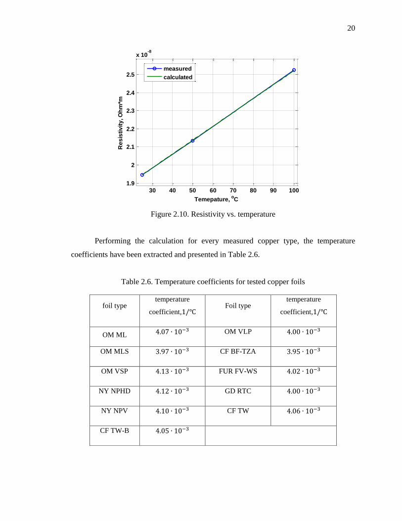
Figure 210 Resistivity vs temperature
Performing the calculation for every measured copper type the temperature
coefficients have been extracted and presented in Table 26
Table 26 Temperature coefficients for tested copper foils
30 40 50 60 70 80 90 100
19
2
21
22
23
24
25
x 10-8
Temepature oC
Re
sis
tiv
ity
O
hm
m
measured
calculated
foil type temperature
coefficient1 Foil type
temperature
coefficient1
OM ML 407 ∙ 10minus3 OM VLP 400 ∙ 10minus3
OM MLS 397 ∙ 10minus3 CF BF-TZA 395 ∙ 10minus3
OM VSP 413 ∙ 10minus3 FUR FV-WS 402 ∙ 10minus3
NY NPHD 412 ∙ 10minus3 GD RTC 400 ∙ 10minus3
NY NPV 410 ∙ 10minus3 CF TW 406 ∙ 10minus3
CF TW-B 405 ∙ 10minus3
21
22 SUMMARY
The LCR Meter with custom probes can be used for the efficient and accurate
measurements of copper resistivity Resistivity values calculated based on LCR meter
measurements converge to those calculated based on measurements taken at the Material
Research Center using Allesi C4S at room temperature Calculated conductivity values at
room temperature of different copper types are 125 lower on average than the nominal
pure copper value σ = 580 ∙ 107 Sm
Further application of Allesi C4S for the temperature dependency measurements
is not possible due to its configuration For this purpose the LCR meter was successfully
utilized at 50 degC and 100degC providing expected linear behavior for resistivity Setup for
these measurements is easy to implement and does not requires using the environmental
chamber achieving the temperature discrepancy below 1 degC Resistivity values of tested
copper types show approximately linear behavior in 25-100 C temperature range
Overall the conductivityresistivity values change with temperature and average
difference between room temperature and 100C is 30 Calculated temperature
coefficients have good agreements with results presented in [8] Particularly the reported
temperature coefficients are in the range form 369 ∙ 10minus3 1C to 409 ∙ 10minus3 1C at
20C and the measured results are in the range from 395 ∙ 10minus3 1C to 413 ∙ 10minus3 1C
Also performed uncertainty estimation shows that the main contribution into the total
error is due to the uncertainty in the trace thickness In order to reduce the error the
actual area of tested samples has to be extracted from the microscopic images of the trace
cross section
22
3 SURFACE ROUGHNESS MODELING
In real PCBs the traces are never smooth and have rough surface causing the
additional loss [29-31] Moreover loss related to surface roughness increases with
frequency and affects the SI performance Since the clock frequencies of modern high
speed devices are in the multi-GHz region the effect of surface roughness cannot be
neglected in general
31 EXPERIMENTAL INVESTIGATION OF SURFACE ROUGHNESS
EFFECTS
For the experimental investigation of the influence of the surface roughness on
losses the set of PCB has been manufactured with different widths and foil types Totally
12 PCB sets were fabricated with every set consisting of six identical PCBs All test lines
are 50 Ohm single ended (SE) striplines and the Megtron6 is used as laminate dielectric
The picture of a typical test vehicle is given in Figure 31 The test board has a ldquothrough-
reflect-linerdquo (TRL) calibration pattern the valid frequency range of the calibration pattern
is at least up to 30 GHz
Figure 31 Picture of the test vehicle
The launch structure is a surface pad designed to accept a flange-mount
compression-fit SMA connectors The 35 mm SMA connectors are mounted on top of
the PCB and are used for excitation The drawing of the SMA connector is presented on
Figure 32
23
Figure 32 Drawing of SMA connector
Three foil types have been implemented for this research Standard foil (STD)
very low profile (VLP) and hyper low profile (HVLP) Roughness parameters for each
of them are provided in Table 31
Table 31 Roughness parameters for three tested foil types [47]
311 Measurement Results and Observations After the TRL calibration the
S-parameters of the 16 inch test lines on all PCBs have been measured Measured
insertion loss of 12 PCBs with different roughness and trace width are illustrated by
Figure 33
Resist Side ℎ119903119898119904 μm Peak to Peak μm
STD 10-20 70-120
VLP 03-04 30-40
HVLP 025-035 20-30
After alt Oxide ℎ119903119898119904 μm Peak to Peak μm
STD 10-20 70-120
VLP 06-10 60-80
HVLP 05-07 40-60
24
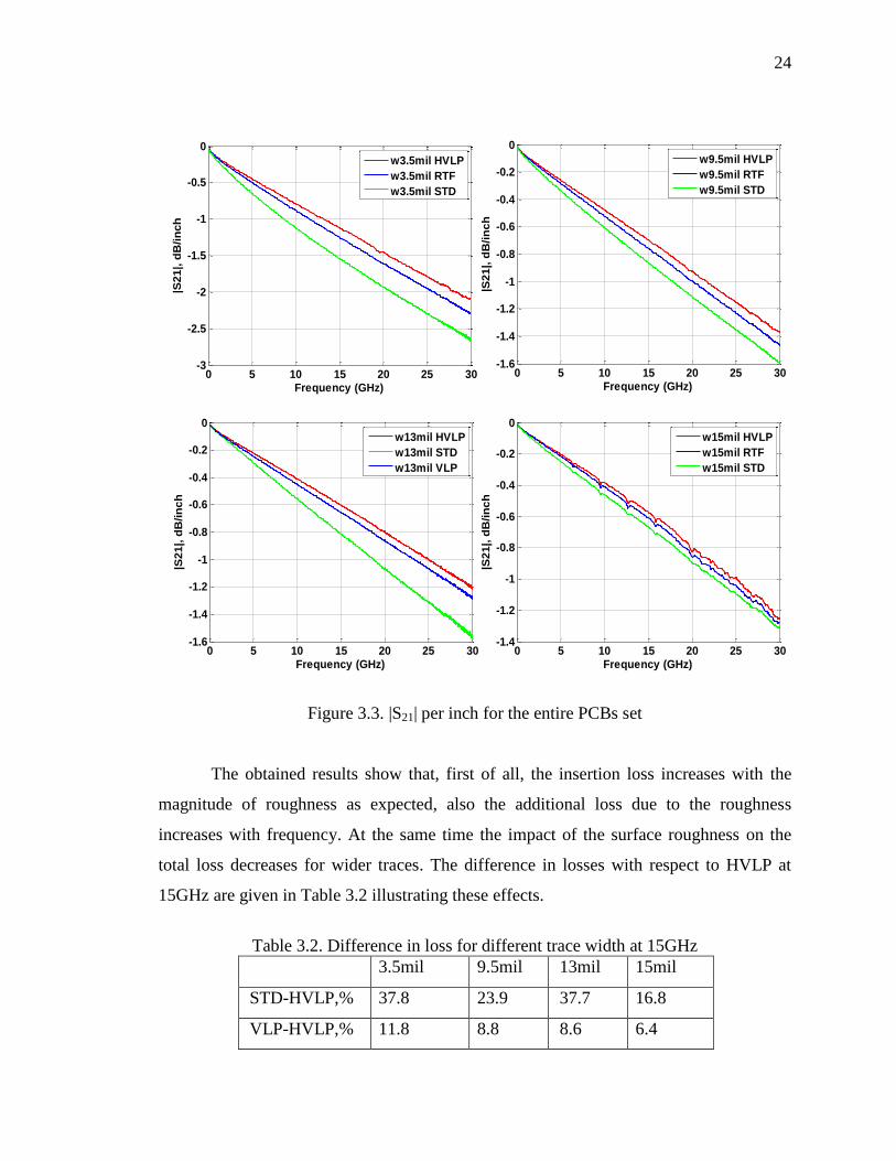
Figure 33 |S21| per inch for the entire PCBs set
The obtained results show that first of all the insertion loss increases with the
magnitude of roughness as expected also the additional loss due to the roughness
increases with frequency At the same time the impact of the surface roughness on the
total loss decreases for wider traces The difference in losses with respect to HVLP at
15GHz are given in Table 32 illustrating these effects
Table 32 Difference in loss for different trace width at 15GHz
35mil 95mil 13mil 15mil
STD-HVLP 378 239 377 168
VLP-HVLP 118 88 86 64
0 5 10 15 20 25 30-16
-14
-12
-1
-08
-06
-04
-02
0
Frequency (GHz)
|S21| d
Bin
ch
w95mil HVLP
w95mil RTF
w95mil STD
0 5 10 15 20 25 30-3
-25
-2
-15
-1
-05
0
Frequency (GHz)
|S21| d
Bin
ch
w35mil HVLP
w35mil RTF
w35mil STD
0 5 10 15 20 25 30-14
-12
-1
-08
-06
-04
-02
0
Frequency (GHz)
|S21| d
Bin
ch
w15mil HVLP
w15mil RTF
w15mil STD
0 5 10 15 20 25 30-16
-14
-12
-1
-08
-06
-04
-02
0
Frequency (GHz)
|S21| d
Bin
ch
w13mil HVLP
w13mil STD
w13mil VLP
25
Another unexpected observation is that the slope of S21 curve increases with
frequency which is particularly visible for HVLP traces
Attenuation coefficient due to the dielectric loss is proportional to the frequency
as 120572119889 = 119862 ∙ 120596 ∙ tan120575 where C is the per unit length (pul) capacitance of the line [6] Since
the conductor loss increases proportionally to the radic120596 (see [1]) at sufficiently high
frequencies the dielectric loss dominates and one should expect almost linear increase of
loss factor for non-dispersive dielectrics The measurements in Figure 33 however show
noticeably non-linear behavior at high frequencies This behavior was observed in other
research groups independently for example as it is shown in Figure 34
Figure 34 Nonlinear behavior of the insertion loss due to the surface roughness [29]
In principle the increase of the slope of S21 could be explained by the frequency-
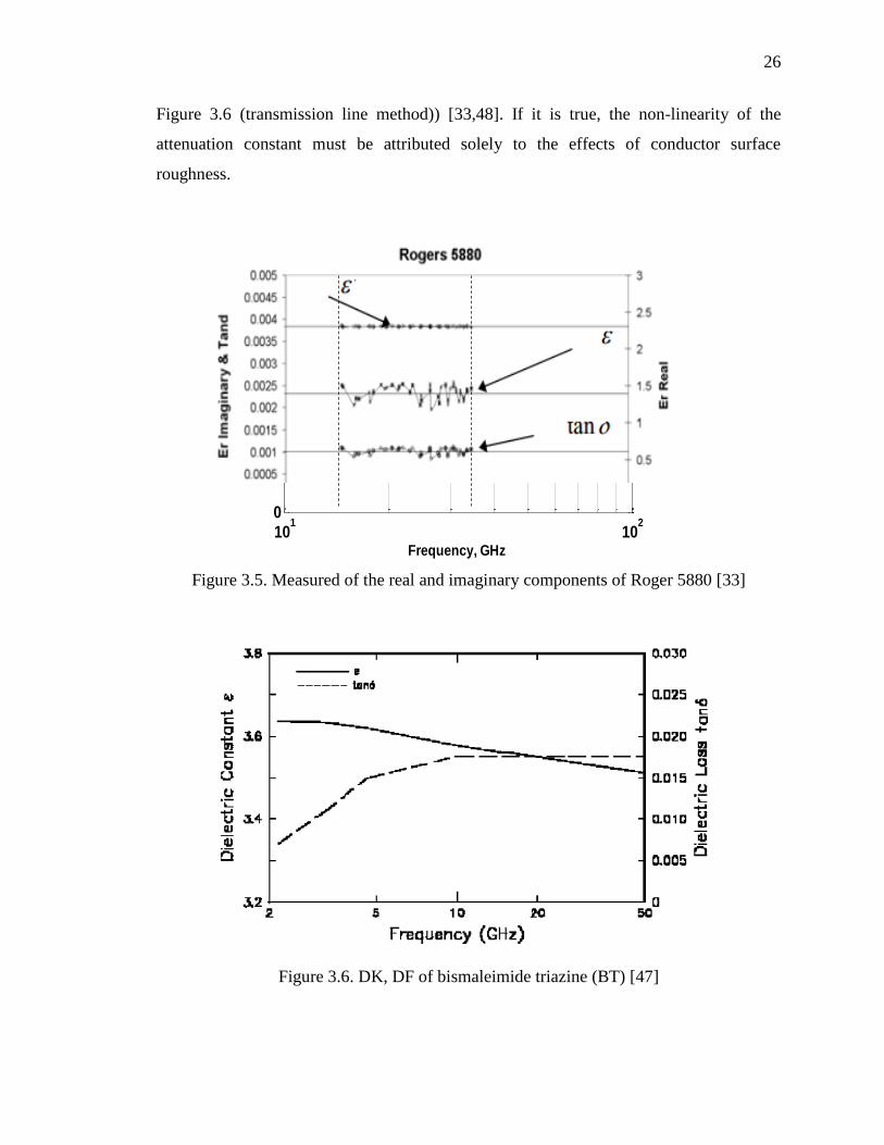
dependent loss in the dielectric in the multi-GHz frequency range (as is done in [32])
however on the other hand there are reports indicating that the low-loss dielectrics
typically used in the PCB design are very low-dispersive above 5 GHz and have nearly
frequency independent tanδ (examples are presented in Figure 35 (resonator method) and
Roughness increases HVLP
to STD
26
Figure 36 (transmission line method)) [3348] If it is true the non-linearity of the
attenuation constant must be attributed solely to the effects of conductor surface
roughness
Figure 35 Measured of the real and imaginary components of Roger 5880 [33]
Figure 36 DK DF of bismaleimide triazine (BT) [47]
101
102
0
02
04
06
08
1
Frequency GHz
27
312 Motivation and Objective Generally these observed effects could not be
explained by any existing models as will be demonstrated in the following section and
calls for the development of the alternative approach Ideally this approach needs to be
physics-based as opposed to phenomenological or behavior modelling A truly physical
approach should involve direct solutions of Maxwellrsquos equations which might be
achieved using one of the commercially available full-wave solvers There are several
challenges that are met when the rough surface is modelled in 3D The obvious one is
that the mesh density (or the number of unknowns) needed to describe the rough surface
of a typical PCB conductor is quite high and might be prohibitive for certain types of
solvers Secondly the high-frequency 3D solvers do not mesh the inner volume of metal
parts but use boundary conditions to model lossy metals instead However the
penetration of field into the metal might be comparable to the size of metal protrusions
due to the roughness and boundary conditions might be not adequate in this situation
And thirdly there are complex chemical compounds that are formed at the interface
between the dielectric and metal [34] which might have quite distinctive electrical
properties Currently there is no way to include the effect of these compounds into the 3D
model because their properties and the thickness of the layer generally are not known
Nevertheless despite these challenges and limitations it was decided to
investigate the possibility to model the rough surfaces of the striplines in full-wave
primarily to get insights into the physics of the roughness-related attenuation
32 EXISTING MODELS FOR SURFACE ROUGHNESS
Many models for conductor surface roughness are based on representation of
roughness profiles by simple shapes In some models the shapes are placed periodically
to simplify the analysis in others the stochastic methods are employed
The usual way to estimate the loss due to rough surface is to calculate the
correction factor or power loss coefficient The power loss coefficient is equal to the ratio
of the attenuation constant due to conductor loses of a transmission line with rough
conductor surfaces to that for the same line with smooth conductor surfaces
321 Hammerstad Model The first model to account for the surface
roughness losses was proposed by Morgan in 1949 [35] In his model the roughness is
28
presented as periodic ldquosaw toothrdquo like structure as shown on Figure 37 The assumption
behind this theory is that current flows along the edge of the rough surface as it is show
on the figure and the additional power losses caused by longer current path Then he used
the finite-difference method to solve a quasi-static eddy-current problem for this
structure As the result the ratio of the power loss dissipated in a conductor with a rough
surface 120630119955119952119958119944119945 to that dissipated in the same but smooth conductor 120630119956119950119952119952119957119945 is calculated
Figure 37 Hammersted model for roughness modeling
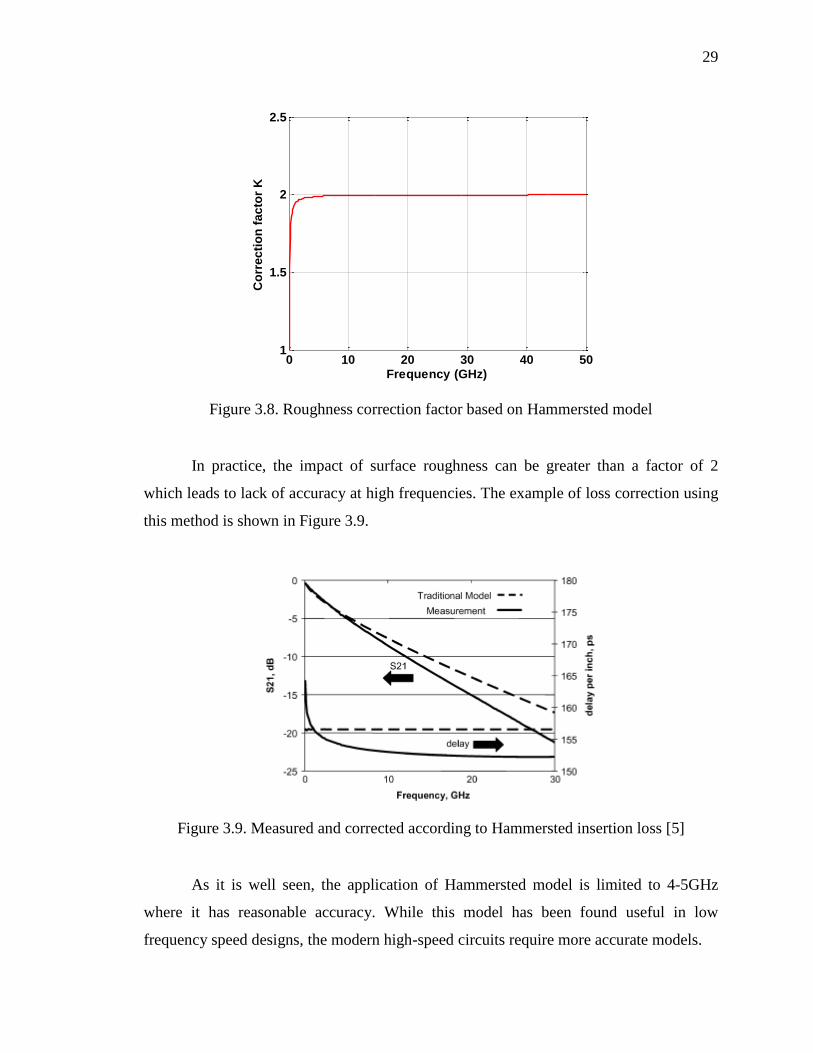
Later Hammerstad and Jensen obtained the empirical expression based on
Morganrsquos results for extra loss and used only one parameter hrms to characterize it [3]
119870119904 =120572119903119900119906119892ℎ
120572119904119898119900119900119905ℎ= 1 +
2
120587∙ 119886119903119888119905119886119899 (14 (
ℎ119903119898119904
120575)
2
) (17)
where 120575 is the skin depth However obtained expression saturates at the value of 2 as it is
shown in Figure 38 for ℎ119903119898119904 = 58119906119898
29
Figure 38 Roughness correction factor based on Hammersted model
In practice the impact of surface roughness can be greater than a factor of 2
which leads to lack of accuracy at high frequencies The example of loss correction using
this method is shown in Figure 39
Figure 39 Measured and corrected according to Hammersted insertion loss [5]
As it is well seen the application of Hammersted model is limited to 4-5GHz
where it has reasonable accuracy While this model has been found useful in low
frequency speed designs the modern high-speed circuits require more accurate models
0 10 20 30 40 501
15
2
25
Frequency (GHz)
Co
rre
cti
on
fa
cto
r K
30
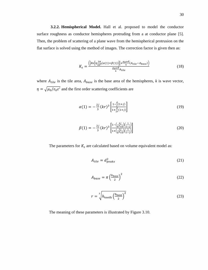
322 Hemispherical Model Hall et al proposed to model the conductor
surface roughness as conductor hemispheres protruding from a at conductor plane [5]
Then the problem of scattering of a plane wave from the hemispherical protrusion on the
flat surface is solved using the method of images The correction factor is given then as
119870119904 =(|119877119890[120578
3120587
41198962(120572(1)+120573(1))]|+1205830120596120575
4(119860119905119894119897119890minus119860119887119886119904119890))
1205830120596120575
4119860119905119894119897119890
(18)
where 119860119905119894119897119890 is the tile area 119860119887119886119904119890 is the base area of the hemispheres k is wave vector
120578 = radic1205830휀0휀prime and the first order scattering coefficients are
120572(1) = minus2119895
3(119896119903)3 [
1minus120575
119903(1+119895)
1+120575
2119903(1+119895)
] (19)
120573(1) = minus2119895
3(119896119903)3 [
1minus(4119895
1198962119903120575)(
1
1minus119895)
1+(2119895
1198962119903120575)(
1
1minus119895)] (20)
The parameters for 119870119904 are calculated based on volume equivalent model as
119860119905119894119897119890 = 1198891199011198901198861198961199042 (21)
119860119887119886119904119890 = 120587 (119887119887119886119904119890
2)
2
(22)
119903 = radicℎtooth (119887base
2)
23
(23)
The meaning of these parameters is illustrated by Figure 310
31
Figure 310 Hemispherical model for roughness modeling
An example of applying Eq(18) with roughness parameters 119887119887119886119904119890 = 94119906119898
119889119901119890119886119896119904 = 94119906119898 휀prime = 4 the correction coefficient in 0 to 50 GHz frequency range is
presented in Figure 311
Figure 311 Roughness correction factor based on Hemispherical model
Application of this model gives relatively accurate results up to 30 GHz [5] as it is
shown on Figure 312
0 10 20 30 40 501
15
2
25
3
Frequency (GHz)
Co
rre
cti
on
fa
cto
r K
32
Figure 312 Measured and corrected according to Hall insertion loss [5]
Hemispherical model is the most popular today and found implementation in
commercial software It is based on three input parameters and requires three statistical
measurements However the accurate measurements of base and space between
protrusions are required On the other hand as can be seen in Figure 312 the model
typically overestimates loss at low frequencies and underestimates at high ones And as
the frequency increases past 30 GHz the underestimation of loss increases
323 Snowball Model In the work of Huray et al the surface roughness is
modeled as a pyramidal stack-up of spherical conductor particles snowballs on a
conductor surface [36-37] as shown in Figure 313
Figure 313 Snowballs model for roughness modeling [36]
33
The problem of scattering and absorption is solved similarly to the hemispherical
model but for every sphere Using the superposition of the sphere losses the total loss of
this structure is derived As the result the roughness correction factor is written as
119870119904 =1205830120596120575
4119860119905119894119897119890+sum 119877119890[120578
3120587
21198962(120572(1)+120573(1))]119873119899=1
1205830120596120575
4119860119905119894119897119890
(24)
Calculated roughness correction factor is presented on Figure 314 Roughness
parameters in this example were the same as in previous model and radii of spheres are
08μm Total number of spheres is N=20
Figure 314 Roughness correction factor based on Snowballs model
This model shows the accurate agreement with measurements up to 50GHz but is
complicate to use The application of this model is shown on Figure 315
0 10 20 30 40 501
15
2
25
3
Frequency (GHz)
Co
rre
cti
on
fa
cto
r K
34
Figure 315 Measured and corrected according to Snowball model insertion loss [5]
As can be seen the agreement at lower frequencies is better but the model also
underestimates loss at higher frequency range
324 Small Perturbation Method Tsang et al conducted more complicated
and deep analysis of the surface roughness problem [38-42] Firstly they analyzed 2D
random rough surfaces based on second order Small Perturbation Method (SPM2) and
numerical method of moments (MoM) [42] Then they performed calculation of power
absorption factor for surface roughness with Gaussian and Exponential correlation
functions Calculations and analysis show that the power absorption enhancement factor
depends on three parameters RMS height correlation length and correlation function
Then this approach has been extended to the analysis of 3D surface roughness
where the surface height varies in both horizontal directions [38] In this work authors
derived the closed-form formula of the power absorption enhancement factor based
119870119904 = 1 +2ℎ2
1205752minus
4
120575int int 119889119896119909119889119896119910119882(119896119909 119896119910)119877119890 radic
2119894
1205752minus 119896119909
2 minus 1198961199102
infin
0
infin
0 (25)
where 119896119909119910 =2120587119899
119871119909119910 and 119882(119896119909 119896119910) is the power spectral density function (PSD)
The example of correction factor calculated using equation (25) is presented on
Figure 316 Calculation was made for roughness profile havingℎ119903119898119904 = 1 119906119898 correlation
length 2 μm and Gaussian function of PSD
35
Figure 316 Roughness correction factor based on SPM2
The comparison of measured and estimated loss show accurate prediction up to 20
GHz and is presented in Figure 317 [39] However this method has been tested only for
ℎ119903119898119904 le 1119906119898 and gives unrealistic correction factor for higher roughness magnitude
Figure 317 Measured and modeled according to SPM2 [39]
0 10 20 30 40 501
11
12
13
14
15
16
17
18
Frequency (GHz)
Co
rre
cti
on
fa
cto
r K
36
325 Scalar Wave Modeling Another model based on the stochastic analysis
is proposed in the work of Chen and Wong In their work [43] the rough surface is
modeled by parameterized stochastic processes The method is based on 3D statistical
modeling of surface roughness and the numerical solution of scalar wave equation The
extra loss caused by surface roughness is approximated by the energy flux absorbed by
the rough surface The scalar wave modeling (SWM) with the method of moments
(MOM) is used to calculate the scattering and absorption of the scalar wave by the rough
surface As the validation of this method the comparison with the SPM2 method was
performed (Figure 318) but not with the experimental results
Figure 318 Roughness correction factor calculated by SWM vs SPM2 [43]
Despite the reported advantages of SWM method it was derived based on scalar
wave theory instead of EM wave theory
326 Limitations of Existing Models As can be seen all of the models
reviewed above improve the accuracy of modelling relative to the case when the surface
roughness is not taken into account The accuracy of prediction is different being the
worst for the Hammersted model and the best for the snowball model However none of
the existing models is capable to capture the effect of increasing slope of the S21 due to
37
the roughness that is evident from Figure 33 and 34 as the correction factors calculated
according to all of them have monotonic second derivative (see Figure 38 311 314
316 318) The slope increase effect can be quite strong adding up to 5 dB loss at 10
GHz (see Figure 34) and definitely requires a closer attention
33 3D MODEL FOR SURFACE ROUGHNESS
The paper [43] proposes the way to generate a surface resembling the real-word
profiles of rough conductors based on the cross-sectional measurements We will follow
a similar procedure to generate the surfaces that can be automatically imported into CST
Microwave Studio
To generate the random roughness the following steps should be taken
Explore the parameters of real roughness Extract statistical parameters
such as probability density function (PDF) Autocorrelation function
(ACR) and ℎ119903119898119904 from the measured roughness profile
Generate the δ-correlated 2D function (surface) with needed PDF
Design a filter and filter the δ-correlated function to obtain a surface with
needed ACR
Import generated surface into CST Microwave studio and perform full
wave simulation
331 Extraction of Roughness Parameters For the surface roughness
characterization the cross section-analysis is essential To perform the cross-sectional
analysis the trace is cut perpendicular to wave propagation direction For this study
several PCB with different foil types have been cut embedded into a special epoxy
compound polished and the microscopic images of the cross-sections are taken Prepared
samples and microscopic images are presented in Figure 319
38
Figure 319 Prepared sample for cross section analysis (a) microscopic pictures of
stripline (b) close-up picture of the trace (c)
The procedure of image processing for PCB cross section analysis is described in
details in [10] After image processing the binary (black-and white) image of the cross-
section is generated The example of the binary image of the VLP trace is shown in
Figure 320
Figure 320 Binary image of the cross-section for VLP
a
b c
10 m
39
The surface roughness profile is extracted directly from the binary images
Roughness profile of the top surface in Figure 320 is shown in Figure 321 and its
autocorrelation function is in Figure 322 The histogram of the profile is presented in
Figure 322
Figure 321 Extracted roughness profile of VLP foil (oxide side)
Figure 322 Autocorrelation function of the VLP foil roughness profile Correlation
length is indicated by the marker
0 10 20 30 40 50 60 70
-2
-15
-1
-05
0
05
1
15
2
xum
Mag
nit
ud
eu
m
-50 0 50
-2
-1
0
1
2
3
4
5
x 104
xum
AC
R
-4 -2 0 2 4
1
15
2
25
3
35
4
45
5
55
x 104
X 1306
Y 2119e+004
xum
AC
R
40
Figure 323 Histogram of VLP foil
The correlation length lACR is defined as the distance where the magnitude of the
autocorrelation function decreases e times and is equal to 13μm in the case on Figure
322 The correlation length can be used to determine the required discretization step as
will be shown later Measured rms height (according to (6)) of the profile is ℎ119903119898119904=081
μm To completely characterize a random function (or a signal) the Probability Density
Function (PDF) is needed however the accurate extraction of it is not possible (as can be
seen in Figure 323) due to limited number of data samples and the normal distribution
was assumed
332 Generation of the 3D Surface In order to create a random surface
firstly a 2D array filled with δ-correlated random numbers is generated The numbers
have normal distribution with zero mean and standard deviation of 1 The adjustment of
the correlation length is achieved by filtering the array by a 2D filter
Generally the filter might be of any kind if it has a needed frequency response
For instance in [43] a Gaussian 2D filter is used However we use 2D finite impulse
response (FIR) low pass filter for simplicity of implementation For the FIR filter of
order N each value of the output sequence 119910[119899] is a weighted sum of the most recent
input values and is given as
-25 -2 -15 -1 -05 0 05 1 15 2 250
200
400
600
800
1000
1200
xum
41
119910[119899] = 1198870119909[119899] + 1198871119909[119899 minus 1] + ⋯ + 119887119873119909[119899 minus 119873] (26)
The internal Matlab function fir1(NWn) is used to generate the 1D prototype
filter Wn is the normalized cut-off frequency which can vary between 0 and 1 where 1
corresponds to the Nyquist frequency Frequency response of such a filter is presented in
Figure 324 for Wn=01 and N=4
Figure 324 Frequency response of a 1D FIR prototype filter
After the 1D prototype filter is generated by the fir1 functions the Matlab
function ftrans2(b) is used to produce the two-dimensional FIR filter that corresponds to
the one-dimensional FIR filter
Examples of frequency response of 2D FIR filters are presented in Figure 325 for
N=4 Wn=01 and N=4 Wn=08
0 02 04 06 08 10
02
04
06
08
1
Normalized Frequency (piradsample)
Ma
gn
itu
ge
42
Figure 325 Frequency responses for Wn=01 (right) and Wn=08 (left) N=4 in both
cases
The gain of the filter produced by the ftrans2 function is 1 at zero frequency In
order to obtain the output array with the desired ℎ119903119898119904 the output of the filter is
multiplied by the gain constant G which is tuned
Then filtering of 2D δ-correlated array by the 2D FIR filter with the frequency
response 119867(1205961 1205962) and multiplication by G gives the final rough surface with
needed ℎ119903119898119904 correlation length and PDF
Described technique provides opportunity to generate surface of any size and
imports it into commercial solvers (technical difficulties of importing are discussed
below) The example of generated surface and realistic surface measured by profilometry
is presented in Figure 326
-1
-05
0
05
1
-1
-05
0
05
10
02
04
06
08
1
Fx
Fy
Magnitude
-1
-05
0
05
1
-1
-05
0
05
104
05
06
07
08
09
1
Fx
Fy
Magnitude
43
Figure 326 Surface roughness profile measured by a profilometer [5] (left) and
generated (right)
It is obvious that the autocorrelation function of the sufficiently long δ-correlated
sequence of values taken at the interval dx will have triangular shape as illustrated by
Figure 327
Figure 327 Autocorrelation function of δ-correlated sequence
Therefore in order to be able to generate a surface with the required correlation
length lACR the discretization step dx should be smaller than the lACR For the example in
Figure 322 the correlation length is equal to 13 μm which means that 119889119909 should be no
more than 13 μm However to produce more realistic profiles the discretization step
-dx dx
ACR
x
44
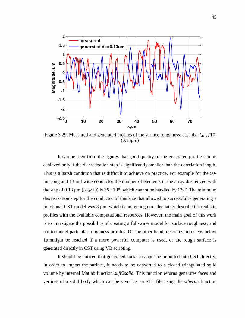
should be much smaller than the lACR This is illustrated by Figure 328 and Figure 329
showing the generated profiles along with the measured one for 119889119909 = 119897119860119862119877 and 119889119909 =
11989711986011986211987710 Parameters of filter to generate roughness with corresponding discretization
steps are given in Table 33
Table 33 Filter parameters for two discretization steps
Figure 328 Measured and generated profiles of the surface roughness with dx=119897119860119862119877
(13μm)
0 10 20 30 40 50 60 70-25
-2
-15
-1
-05
0
05
1
15
2
xum
Mag
nit
ud
e u
m
measured
generated
dx=013 μm (l10) dx=13 μm (l)
Wn 003575 067787
N 22 4
G 15646 1414
45
Figure 329 Measured and generated profiles of the surface roughness case dx=11989711986011986211987710
(013μm)
It can be seen from the figures that good quality of the generated profile can be
achieved only if the discretization step is significantly smaller than the correlation length
This is a harsh condition that is difficult to achieve on practice For example for the 50-
mil long and 13 mil wide conductor the number of elements in the array discretized with
the step of 013 μm (lACR10) is 25 ∙ 106 which cannot be handled by CST The minimum
discretization step for the conductor of this size that allowed to successfully generating a
functional CST model was 3 μm which is not enough to adequately describe the realistic
profiles with the available computational resources However the main goal of this work
is to investigate the possibility of creating a full-wave model for surface roughness and
not to model particular roughness profiles On the other hand discretization steps below
1μmmight be reached if a more powerful computer is used or the rough surface is
generated directly in CST using VB scripting
It should be noticed that generated surface cannot be imported into CST directly
In order to import the surface it needs to be converted to a closed triangulated solid
volume by internal Matlab function sufr2solid This function returns generates faces and
vertices of a solid body which can be saved as an STL file using the stlwrite function
0 10 20 30 40 50 60 70-25
-2
-15
-1
-05
0
05
1
15
2
xum
Mag
nit
ud
e u
m
measured
generated dx=013um
46
(open-source implementation) [48] The STL file generated by stlwrite can be imported
directly to CST or any other 3D solver that supports it
333 Surface Roughness Modeling in CST Microwave Studio Because of
the small-scale details of the rough surface the full wave simulations of it require very
fine mesh This leads to extremely high requirements for memory and CPU power which
restricts the size of modeled structure That is why the stripline model needs to be as
short as possible To perform the full-wave simulation the 54mil long 13 mil width
stripline was created in CST To maintain the 50 Ohm characteristic impedance a
dielectric with ε=43 and tanδ=0005 (representing a low-loss dielectric like Megtron 6)
was used The cross-section of the signal conductor is 3x13mil and the distance between
the ground planes is 195 mil The vertical boundary conditions were set to magnetic
walls to represent infinite span of the ground planes A solid with the rough surface was
generated in Matlab as described above and imported to CST as an additional layer added
on top of the smooth central conductor The length of the rough solid is 50 mil leaving 2
mil of smooth conductor adjacent to both waveguide ports to allow performing correct
excitation of the structure by the ports The discretization step was set to 4 μm All
conductors are modelled as lossy metal with 120648 = 120787 120790 ∙ 120783120782120789 Sm
It is important to notice that in order to reach the correlation length close to real
roughness the discretization step should be less than 1μm However such small step
makes it impossible to import generated roughness to CST The minimum step which
allows to run simulation is 2 μm and higher
The implementation of the stripline structure with rough surface is presented in
Figure 330 and Figure 332 To minimize the mesh requirements two symmetry planes
were defined (as shown in Figure 331 reducing the total number of mesh cells
approximately by 4
47
Figure 330 Stripline structure to model the surface roughness
Figure 331 Boundary condition and planes of symmetry used for simulation Blue ndash
magnetic walls green ndash electric walls
Figure 332 Zoom of the end of the trace with surface roughness
48
The frequency domain FEM solver was chosen for full wave analysis for two
reasons Firstly the generated rough surface is naturally described by a tetrahedral mesh
used in the FEM solver And secondly the transmission coefficients calculated by the
FEM solver do not suffer from truncation errors common for the time-domain solver
resulting in ldquoripplesrdquo in the obtained curves The amplitude of these parasitic ripples
might be comparable to the effect of roughness itself making the investigation with the
TD solvers virtually impossible
The efficiency of the model is demonstrated by the Table 34 showing the total
number of tetrahedrons and simulation time per 1 frequency for different values of dx
Table 34 Tetrahedrons and time required for different discretization step
dx μm Tetrahedrons Time per
frequency
60 41892 09 min
50 58657 12 min
40 82551 25 min
30 210209 43 min
As can be seen the model is quite efficient requiring only 4 min per frequency
for dx=3 μm Extrapolating the results in the table the simulation time per frequency for
dx=1 μm and dx=01 μm can be estimated as 45 min and 5500 min (38 days)
correspondingly
Besides the simulation time some time is spent on the importing of the rough
surface This time can be relatively long reaching 10 min for dx=3 μm however this
operation needs to be performed only once per model
334 Results and Discussion Firstly several simulations for different
discretization steps changing from 3 to 6 μm were performed The maximum difference
in dB(S21) obtained for different discretization step was less than 1 in the entire
frequency range which means that for this particular model the discretization step of 6
μm can be used (which provides short simulation time allowing to perform parametric
sweeps easily) without loss of accuracy For further simulations the dx=5 μm was used
As the next step the simulations were done for different roughness
magnitude ℎ119903119898119904 In order to do it the rescaling function was used in CST which allowed
49
avoiding regenerating the rough surface and reimporting it into CST This can be done
because different realizations of the rough surface produce virtually indistinguishable
transmission coefficients as demonstrated by Figure 333
Figure 333 Five different realization of surface with the same parameters
The result of the hrms sweep is presented in Figure 334 along with the
corresponding experimental result from the literature [29]
Figure 334 Modeled (a) and measured (b) insertion loss for different roughness
magnitude up to 10 GHz
At the first glance the obtained results agree very well with the measurements
showing the same tendency of increasing slope of the curve
0 10 20 30 40 50-15
-1
-05
0
Frequency (GHz)
|S21|in
ch
d
B
surface1
surface2
surface3
surface4
surface5
0 2 4 6 8 10
-05
-04
-03
-02
-01
0
Frequency (GHz)
|S21|in
ch
d
B
h rms 193um
h rms 232um
h rms 270um
h rms 308um
h rms 347um
h rms 386um
smooth
Roughness
increases HVLP
to STD
50
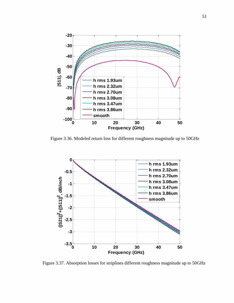
However upon closer examination it was noticed that the change of S21 slope is
due to the change of the reflection coefficient due to the roughness It can be better
understood if the plots of S21 (Figure 335) and S11 (Figure 336) are analyzed together up
to 50 GHz It is obvious that the increased insertion loss corresponds to the increased
reflection loss and is actually caused by it not by the roughness This effect happens
because the line is extremely short and has very small absolute value of insertion loss
such that even very weak reflections on the order of -20 to -40 dB might affect the
transmission To demonstrate it the transmission loss was corrected by calculating
|S21|2+|S11|
2 (this quantity shows the absorption loss in the transmission line) As can be
seen from Figure 337 the slope of the absorption loss curve remains constant above a
certain frequency however it does depend on the roughness magnitude This result is
very close to the results obtained by all other models reviewed in Section 32
To minimize the effect of reflections the length of the transmission line was
increased by multiplying the rough segment 2 4 and 8 times As can be seen from
Figures 338 339 340 the contribution of the reflection loss to the slope decreases with
the length of the line and for the length of 400 mil (x8) the correction for the reflection
loss is not needed
Figure 335 Modeled insertion loss for different roughness magnitude up to 50GHz
0 10 20 30 40 50-16
-14
-12
-1
-08
-06
-04
-02
0
Frequency (GHz)
|S2
1|in
ch
d
B
h rms 193um
h rms 232um
h rms 270um
h rms 308um
h rms 347um
h rms 386um
smooth
51
Figure 336 Modeled return loss for different roughness magnitude up to 50GHz
Figure 337 Absorption losses for striplines different roughness magnitude up to 50GHz
0 10 20 30 40 50-100
-90
-80
-70
-60
-50
-40
-30
-20
Frequency (GHz)
|S1
1| d
B
h rms 193um
h rms 232um
h rms 270um
h rms 308um
h rms 347um
h rms 386um
smooth
0 10 20 30 40 50-35
-3
-25
-2
-15
-1
-05
0
Frequency (GHz)
(|S
21
|)2+
(|S
11
|)2
dB
in
ch
h rms 193um
h rms 232um
h rms 270um
h rms 308um
h rms 347um
h rms 386um
smooth
52
Figure 338 Modeled insertion losses for different length of stripline
Figure 339 Modeled return losses for different length of stripline
0 10 20 30 40 50-16
-14
-12
-1
-08
-06
-04
-02
0
Frequency (GHz)
|S2
1|in
ch
d
B
2xlength
4xlength
8xlength
smooth
0 10 20 30 40 50-100
-90
-80
-70
-60
-50
-40
-30
-20
Frequency (GHz)
|S1
1| d
B
2xlength
4xlength
8xlength
smooth
53
Figure 340 Absorption losses for striplines of different length up to 50GHz
The obtained results demonstrate that it is possible to build a realistic full-wave
model of a stripline with rough conductors that can be solved easily on workstations
without the need for clusters or super-computers
At the same time the model failed to reproduce the frequency dependent slope of
S21 curves observed independently in many measurements This might indicate that our
understanding of physical processes in transmission lines with roughness requires
refinement The proposed full-wave model does not take into account penetration of field
into metal effect of chemical compounds at the interface metal-dielectric inhomogeneity
and anisotropy of the dielectric which might be responsible for the roughness effect
Potentially quantum effects might also be relevant
0 10 20 30 40 50-35
-3
-25
-2
-15
-1
-05
0
Frequency (GHz)
(|S
21
|)2+
(|S
11
|)2
dB
in
ch
2xlength
4xlength
8xlength
smooth
54
4 CONCLUSION
The research presented in this thesis is dedicated to conductor-related loss in
PCB There are two sources of conductor losses ndash skin effect which relates to the finite
metal conductivity and the effect of surface roughness The conductivity of copper and its
temperature dependency were investigated experimentally The effect of surface
roughness was modeled using full wave simulation in CST Microwave Studio
Conductivity of eleven copper types was evaluated using four probe technique at
three temperatures It should be noted that obtained conductivity values are different for
all eleven copper types and are lower than nominal values of copper at room temperature
Whereas extracted temperature coefficients converge to values found in literature
Obtained results can be used in simulation related to signal integrity analysis and might
prevent the underestimation of actual loss in transmission line This should be taken into
account to better perform the signal integrity analysis
For surface roughness investigation the set of PCBs with different foil types and
trace widths has been measured Obtained S21 curves show expected results - losses
increase in rough traces However it was also shown that in low loss transmission line
there is unusual behavior of S21 ndash the slope becomes frequency dependent Literature
review confirms this observation however there was no explanation found of this effect
As an attempt to investigate and understand the nature of this observation numerous full
wave simulations have been performed for generated 3D rough surface Although this
model fails to predict frequency dependent slope of S21 curves the methodology
proposed in this work for 3D rough surface generation compatible with EM solvers can
be used for further roughness effect investigation
55
BIBLIOGRAPHY
[1] EBogatin Signal Integrity- simplified Upper Saddle River NJ Pearson
Education Inc 2004
[2] S Hall and H Heck Advanced Signal Integrity for High-Speed Digital Designs
New York NY USA Wiley 2009
[3] O Jensen and E Hammerstand Accurate models for microstrip computer-aided
design IEEE MTT-S Digest pp 407-409 1980
[4] G Brist S Clouser and T Liang Non-classical conductor losses due to copper
foil roughness and treatment ECW 10 Conf at IPC Circuits Designers Summit
pp S19-2-1-S19-2-1-11 2005
[5] S Hall S Pytel P Huray D Hua A Moonshiram G Brist and E Sijercic
ldquoMultigigahertz causal transmission line modeling methodology using a 3-D
hemispherical surface roughness approach Microwave Theory and Techniques
IEEE Transactions on vol 55 no 12 pp 2614-2624 Dec 2007
[6] D M Pozar Microwave Engineering 2nd ed Wiley New York NY 1998
[7] R A Matula ldquoElectrical Resistivity of Copper gold Palladium and Silverrdquo J
Phys Chem RefData Vol8 No4 1979
[8] S Hinaga MY Koledintseva ldquoThermal Effects on PCB Laminate Material
Dielectric Constant and Disipation Factorrdquo Techn Conf IPC ExpoAPEX 2010
Las Vegas April 5-8 2010
[9] ldquoCopper-Foils-for-High-Frequency-Circuit-Materialsrdquo available at
httpswwwrogerscorpcomdocμments749acsCopper-Foils-for-High-
Frequency-Circuit-Materialspdf
[10] S De A Gafarov M Koledintseva S Hinaga R J Stanley J Drewniak
ldquoSemi-Automatic Copper Foil Surface Roughness Detection from PCB
Microsection Imagesrdquo 2012 IEEE International Symposium on Electromagnetic
Compatibility (EMC)
[11] Y Shlepnev ldquoDielectric and Conductor Roughness Models Identification for
Successful PCB and Packaging Interconnect Design up to 50 GHzrdquo The PCB
Design Magazine 022014 2014(2)12-28
56
[12] Gary Brist Stephen Hall Sidney Clouser amp Tao Liang ldquoNon-Classical Conductr
Losses Due to copper Foil Roughness and Treatmentrdquo ECWC 10 Conference at
IPC Printed Circuits Expo SMEMA Council APEX and Designers Summit 05
[13] Lazarus Weiner Premo Chiotti H A Wilhelm ldquoTemperature dependence of
electrical resistivity of metalsrdquo United States Atomic Energy Commission
Technical Information Service 1952
[14] Lorenz L III Concerning the Conductivity of Metals for Heat and Electricity
Ann Phys 3 13 582-606 1881
[15] Jaeger W and Diesselhorst H ldquoThermal Conductivity Electrical Conductivity
Heat Capacity and Thermoelectric Power of Several Metalsrdquo Wiss Abh Phys-
Tech Reichsanst 3 269-425 1900
[16] J H Dellinger ldquoThe Temperature Coefficient of Resistance of Copperrdquo Bulletin
of the Bureau of Standards Vol7 No1 1900
[17] Niccolai G ldquoElectrical Resistivity of Metals Between Very High and Very Low
Temperaturesrdquo Phys Z 9(11) 367-72 1908
[18] Northrup EF ldquoResistivity of Copper in Temperature Range 20C to 1450Crdquo J
Franklin Inst 177(1) 1-21 1914
[19] S W Stratton ldquoCopper wire tablesrdquo United States National Bureau of Standards
3d Ed No31 Oct 1 1914
[20] Gruneisen E and Goens E ldquoInvestigation of Metal Crystals V electrical and
Thermal Conductivity of Single and Polycrystalline Metals of Regular Systemsrdquo
Z Phys 44 615-42 1927
[21] Laubitz M J ldquoTransport Properties of Pure Metals at high Temperatures I
Copperrdquo Can J Phys 45(11) 3677-96 1967
[22] Smits F M ldquoMeasurements of Sheet Resistivity with the Four-Point Proberdquo
Bell Syst Tech J195837371
[23] Valdes L ldquoResistivity Measurements on Germanium for Transistorsrdquo Proc IRE
42 420 1954
[24] ldquoEvaluation of measurement data mdash Guide to the expression of uncertainty in
measurementrdquo Joint Committee for Guides in Metrology (JCGM) 1002008
57
[25] Taylor John An Introduction to Error Analysis 2nd ed University Science
Books Sausalito 1997
[26] Baird DC Experimentation An Introduction to Measurement Theory and
Experiment Design 3rd ed Prentice Hall Englewood Cliffs 1995
[27] Lichten William Data and Error Analysis 2nd ed Prentice Hall Upper Saddle
River NJ 1999
[28] Bevington Phillip and Robinson D Data Reduction and Error Analysis for the
Physical Sciences 2nd ed McGraw-Hill New York 1991
[29] A Ippich ldquoA Designs Experiment for the Influence of Copper Foils on
Impedance DC Line Resistance and Insertion Lossrdquo IPC APEX Expo 2012
[30] Lee B ldquoThe Impact of Inner layer Copper Foil Roughness on Signal Integrityrdquo
Printed Circuit Design and Fab April 2007
[31] Briest G and Hall S ldquoNon-Classical Conductor Losses due to Copper Foil
Roughness and Treatmentrdquo IPC Printed Circuit Expo 2005
[32] Y Shlepnev A Neves T Dogostino S McMorrow ldquoMeasurement-Assisted
Electromagnetic Extraction of Interconnect Parameters on Low- Cost FR-4 boards
for 6-20 Gbsec Applications ldquoDesignCon 2009
[33] S G Pytel G Barnes D Hua A Moonshiram G Brist R Mellitz S Hall and
P G Huray ldquoDielectric modeling characterization and validation up to 40
GHzrdquo presented at the 11th Signal Propag on Interconnects Workshop Genoa
Italy May 13ndash16 2007
[34] S Hinaga M Koledintseva P K Reddy Anmula amp J L Drewniak ldquoEffect of
conductor surface roughness upon measured loss and extracted values of PCB
laminate material dissipation factorrdquo IPC APEX Expo 2009 Conference La
Vegas March 2009
[35] S P Morgan ldquoEffect of surface roughness on eddy current losses at microwave
frequencies Journal of Applied Physics vol 20 no 4 pp 352-362 Apr 1949
[36] P Huray S Hall S Pytel F Oluwafemi R Mellitz D Hua and P Ye
ldquoFundamentals of a 3-D snowball model for surface roughness power losses in
Signal Propagation on Interconnects 2007 SPI 2007 IEEE Workshop on May
2007 pp 121-124
58
[37] P G Huray O Oluwafemi J Loyer E Bogatin and X Ye ldquoImpact of copper
surface texture on loss A model that works DesignCon 2010 Proceedings 2010
[38] L Tsang X Gu and H Braunisch ldquoEffects of random rough surface on
absorption by conductors at microwave frequencies Microwave and Wireless
Components Letters IEEE vol 16 no 4 pp 221-223 April 2006
[39] X Gu L Tsang and H Braunisch ldquoEstimation of roughness-induced power
absorption from measured surface profile data Microwave and Wireless
Components Letters IEEE vol 17 no 7 pp 486-488 July 2007
[40] H Braunisch X Gu A Camacho-Bragado and L Tsang ldquoOn-chip rough-metal-
surface propagation loss modeling and correlation with measurements in
Electronic Components and Technology Conference 2007 ECTC 07
Proceedings 57th May 2007 pp 785-791
[41] L Tsang X Gu and H Braunisch ldquoEffects of random rough surface on
absorption by conductors at microwave frequenciesrdquo IEEE Microw Wireless
Compon Lett vol 16 no 4 pp 221ndash223 Apr 2006
[42] X Gu L Tsang H Braunisch and P Xu ldquoModeling absorption of rough
interface between dielectric and conductive mediumrdquo Microw Opt Technol
Lett vol 49 pp 7ndash13 Jan 2007
[43] Q Chen and N Wong ldquoNew Simulation Methodology of 3D Surface Roughness
Loss for Interconnectsrdquo Design Automation and Test in Europe DATE 2009
Nice France April 20-24 2009
[44] In Intelligent Signal Processing and Communications 2006 ISPACS 06
International Symposium on Dec 2006 pp 411-414
[45] Advanced Design System Retrieved from httpwwwkeysightcomenpc-
1297113advanced-design-system-adscc=USamplc=eng
[46] J A Marshall ldquoMeasuring Copper Surface Roughness for High Speed
Applicationsrdquo Retrieved from
httpwwwcircuitinsightcompdfmeasuring_copper_surface_roughness_ipcpdf
[47] A Deutsch et ldquoExtraction of εr(f)and tanδ(f) for Printed Circuit Board
Insulators Up to 30 GHz Using the Short-Pulse Propagation Techniquerdquo IEEE
Transactions on Advanced Packaging vol28 no1 Feb 2005
59
[48] Export a variety of inputs (patch surface) to an STL triangular mesh (30 Jul
2008) Retrieved from
httpwwwmathworkscommatlabcentralfileexchange20922-stlwrite-filename--
varargin-
60
VITA
Mr Oleg Kashurkin was born in Russia He received his State Specialist Diploma
(equivalent MS) degree in Physics with specialization in Radiophysics and Electronics
from Department of Science Peoples Friendship University of Russia in June 2006
In 2008-2011 he worked as Sr Engineer in Laboratory of Microwave Composite
at Institute for Theoretical and Applied Electromagnetics Russian Academy of Science
In August 2013 he joined the EMC Laboratory of Missouri University of Science
and Technology as the graduate student and has been working as a research assistant In
May 2016 he received his Master Degree in Electrical Engineering from Missouri
University of Science and Technology
- Measurements and simulation of conductor-related loss of PCB transmission lines
-
- Recommended Citation
-
- tmp1467300612pdf4BHfj
-

MEASUREMENTS AND SIMULATION OF CONDUCTOR-
RELATED LOSS OF PCB TRANSMISSION LINES
by
OLEG KASHURKIN
A THESIS
Presented to the Faculty of the Graduate School of the
MISSOURI UNIVERSITY OF SCIENCE AND TECHNOLOGY
In Partial Fulfillment of the Requirements for the Degree
MASTER OF SCIENCE IN ELECTRICAL ENGINEERING
2016
Approved by
Victor Khilkevich Advisor
David Pommerenke
Jun Fan
2016
Oleg Kashurkin
All Rights Reserved
iii
ABSTRACT
With continuously increasing data rates Signal Integrity (SI) problems become
more and more challenging One of the main issues in high-speed data transfer is the
frequency-dependent loss of transmission lines This thesis is dedicated to conductor-
related loss mechanisms in printed circuit board (PCB) transmission lines
This thesis provides the experimental investigation of conductor properties used
for fabrication of PCBs Particularly the resistivity and conductivity along with the
temperature coefficients of eleven copper types is measured and reported A four probe
measurement technique is used Results were verified by two independent measurements
and show discrepancy of less than 05
Another major conductor-related loss mechanism is the attenuation of the
electromagnetic waves due to the surface roughness of PCB conductors There are
several models attempting to take into account the roughness effect However none of
them are able to explain or predict the transmission line behavior with high accuracy
Particularly the experimental observations show that the slope of S21 curves increases
with frequency which cannot be modelled by the existing model To better understand
the physics associated with the loss due to the surface roughness of conductors and be
able to predict the behavior of transmission lines in the future a full wave model of
surface roughness was developed The detailed methodology for 3D roughness
generation is provided
iv
ACKNOWLEDGMENTS
I would like to express my sincere gratitude and deep appreciation to my advisor
Dr Victor Khilkevich for guidance toward my academic path ideas and help with
experiment conducting technique I am very thankful him for introduction to real world
electrical engineering revel modern and challenge problems of high-speed design and
EMC I express my sincere gratitude to Dr Marina Y Koledintseva for her constant
support and inspiration for work I thank Dr James L Drewniak for his mentoring and
guidance in my career and manage project I was involved in as part of the EMC
Laboratory and for giving me this opportunity to be a member of EMC lab I am very
grateful to Mr Scott Hinaga from Cisco Systems Inc for his encouragement attention to
new ideas and techniques and exceptional help throughout my project work
I want to show my deep gratitude to all professors of the EMC Laboratory for
giving me priceless knowledge during course work and showing faith in me as a graduate
student I greatly appreciate classes of Dr David Pommerenke and Dr Jun Fan which
straightened my understanding of Electromagnetics and Wave propagation Theory I
thank all my fellow laboratory students who gave me advice and helped me to go
through any problems I encountered
Finally I would like to thank my beloved family especially my wife Tatiana
Platova for her endless and unconditional love support and encouragement through all
my education and life
This thesis is based upon work supported partially by the National Science
Foundation under Grant No IIP-1440110
v
TABLE OF CONTENTS
Page
ABSTRACT iii
ACKNOWLEDGMENTS iv
LIST OF ILLUSTRATIONS vii
LIST OF TABLES ix
NOMENCLATURE x
SECTION
1 INTRODUCTION 1
11 CONDUCTOR ndash RELATED LOSS IN TRANSMISSION LINE 2
2 MEASUREMENT OF COPPER RESISTIVITY 6
21 BACKGROUND 6
211 Four-Probe Technique 8
212 Setup 9
213 DUT Description 12
214 Uncertainty Estimation 13
215 Results and Discussion 15
22SUMMARY 21
3 SURFACE ROUGHNESS MODELING 22
31 EXPERIMENTAL INVESTIGATION OF SURFACE ROUGHNESS
EFFECTS 22
311 Measurement Results and Observations 23
312 Motivation and Objective 27
32 EXISTING MODELS FOR SURFACE ROUGHNESS 27
321 Hammerstad Model 27
322 Hemispherical Model 30
323 Snowball Model 32
324 Small Pertrubation Method 34
325 Scalar Wave Modeling 36
326 Limitations of Existing Models 36
vi
33 3D MODEL FOR SURFACE ROUGHNESS 37
331 Extraction of Roughness Parameters 37
332 Generation of the 3D Surface 40
333 Surface Roughness Modeling in CST Microwave Studio 46
334 Results and Discussion 48
4 CONCLUSION 54
BIBLIOGRAPHY 55
VITA 60
vii
LIST OF ILLUSTRATIONS
Figure Page
11 Modeled transmission coefficients of stripline at 25 and 125 4
12 Optical microscopic images of roughness From left to right STD (standard)
VLP (very low profile) HVLP (hyper very low profile) 5
13 Hall Hemispherical model used in ADS [5] (a) GMS model developed in
Simberian Inc [11] (b) 5
21 Schematic of Four - Point Probe Technique 8
22 Pogo pin (left) Customized probes for resistivity measurements (right) 9
23 Setup schematic for resistance measurements 10
24 Setup for resistance measurements (a) window for probes landing (b) two
thermocouples placed on the DUT (c)11
25 Top layer of tested coupon 12
26 The cross section of the tested trace 13
27 Allesi C4S 4-point probe 16
28 Conductivity over temperature for all tested copper types 19
29 Resistivity over temperature for all tested copper types 19
210 Resistivity vs temperature 20
31 Picture of the test vehicle 22
32 Drawing of SMA connector 23
33 |S21| per inch for the entire PCBs set 24
34 Nonlinear behavior of the insertion loss due to the surface roughness [29] 25
35 Measured of the real and imaginary components of Roger 5880 [33] 26
36 DK DF of bismaleimide triazine (BT) [47] 26
37 Hammersted model for roughness modeling 28
38 Roughness correction factor based on Hammersted model 29
39 Measured and corrected according to Hammersted insertion loss [5] 29
310 Hemispherical model for roughness modeling 31
311 Roughness correction factor based on Hemispherical model 31
312 Measured and corrected according to Hall insertion loss [5] 32
313 Snowballs model for roughness modeling [36] 32
viii
314 Roughness correction factor based on Snowballs model 33
315 Measured and corrected according to Snowball model insertion loss [5] 34
316 Roughness correction factor based on SPM2 35
317 Measured and modeled according to SPM2 [39] 35
318 Roughness correction factor calculated by SWM vs SPM2 [43] 36
319 Prepared sample for cross section analysis (a) microscopic pictures of stripline
(b) close-up picture of the trace (c) 38
320 Binary image of the cross-section for VLP38
321 Extracted roughness profile of VLP foil (oxide side) 39
322 Autocorrelation function of the VLP foil roughness profile Correlation length
is indicated by the marker 39
323 Histogram of VLP foil 40
324 Frequency response of a 1D FIR prototype filter 41
325 Frequency responses for Wn=01 (right) and Wn=08 (left) N=4 in both cases 42
326 Surface roughness profile measured by a profilometer [5] (left) and generated
(right) 43
327 Autocorrelation function of δ-correlated sequence 43
328 Measured and generated profiles of the surface roughness with dx=lACR
(13μm) 44
329 Measured and generated profiles of the surface roughness with dx=l11986011986211987710
(013μm) 45
330 Stripline structure to model the surface roughness 47
331 Boundary condition and planes of symmetry used for simulation Blue ndash
magnetic walls green ndash electric walls 47
332 Zoom of the end of the trace with surface roughness 47
333 Five different realization of surface with same parameters 49
334 Modeled (a) and measured (b) insertion loss for different roughness magnitude
up to 10 GHz 49
335 Modeled insertion loss for different roughness magnitude up to 50GHz 50
336 Modeled return loss for different roughness magnitude up to 50GHz 51
337 Absorption losses for striplines different roughness magnitude up to 50GHz 51
338 Modeled insertion loss for different length of stripline 52
339 Modeled return loss for different length of stripline 52
340 Absorption losses for striplines of different length up to 50GHz 53
ix
LIST OF TABLES
Table Page
21 Values for the electrical resistivity and temperature coefficients of annealed
copper 7
22 Thickness width and area of traces 14
23 Comparison of conductivity obtained by two methods (3 copper types are
shown) 16
24 Conductivity at room temperature 50 C and 100 C 17
25 Resistivity at room temperature 50 C and 100 C 18
26 Temperature coefficients for tested copper foils 20
31 Roughness parameters for three tested foil types [47] 23
32 Difference in loss for different trace width at 15GHz 24
33 Filter parameters for two discretization steps 44
34 Tetrahedrons and time required for different discretization step 48
x
NOMENCLATURE
Symbol Description
E Electric field vector
E0 Electromagnetic wave amplitude
ω Angular frequency
119891 Frequency
k Wave number
120574 Propagation constant
120572 Total attenuation constant
120573 Phase constant
120572119888 Conductor loss
120572119889 Dielectric loss
120575 Skin depth
120590 Conductivity of metal
120583 Absolute permeability
ε Absolute permittivity
120588 Resistivity
ρ0 Resistivity at reference temperature
T0 Reference temperature
αT Temperature coefficient
ℎ119903119898119904 ldquoroot-mean-squaredrdquo (RMS) value of surface roughness magnitude
119869 Current density
xi
I Current
A Cross section area of the trace
119909120583 Mean value of sequence
R Resistance
S Standard deviation
∆119906 Standard uncertainty
∆120588 Uncertainty in resistivity
119870119904 Power loss coefficient
Atile Title area
119860119887119886119904119890 Base area of the hemispheres
W(kx ky) Power spectral frequency function
119897ACR Correlation length
Wn Normalized cut-off frequency
G Gain of the FIR filter
1 INTRODUCTION
The complexity of design and rapidly increasing data rate in high-speed digital
electronics makes the signal integrity performance hard to maintain As the data rate
increases the loss in transmission lines becomes the main issue for signals with clock
higher than 1GHz [1] As a signal propagates along a transmission line the frequency
dependent loss causes the signal degradation as the high-frequency part of the spectrum
experiences higher attenuation A transmission line with high loss causes more signal
distortion and limits the speed of the transmitted data This makes it important to
determine the high-frequency loss behavior in PCBs at the design stage
There are several mechanisms of loss in transmission lines but the primary ones
are conductor loss dielectric loss and loss due to the surface roughness of the traces [1]
Models of transmission lines need to take into account all three physical loss
mechanisms The conductor and dielectric loss are relatively well studied and good
models for them exist [2] In order to use these models the parameters of materials need
to be determined by measurement The conductor loss is equally important as the
dielectric loss but it is typical to use nominal value for the resistivity of copper to model
PCB transmission lines [1 2] In this work a practical and easy-to-implement method for
the conductor loss measurement (including temperature dependency) is presented The
obtained results indicate that the actual resistivity of copper used to create PCB
interconnects is noticeably lower than the nominal value and needs to be measured in
order to improve the accuracy of the transmission line modeling
Another very important factor determining the loss of PCB transmission lines is
the surface roughness of copper layers [3][4] Despite its importance there is still no
satisfactory understanding of physical mechanisms responsible for the roughness-related
attenuation and existing models do not provide enough accuracy in many cases as will be
shown further In this work a new full-wave model of conductor surface roughness is
proposed that can be used to investigate physical effect associated with conductor
surface roughness
2
11 CONDUCTOR ndash RELATED LOSS IN TRANSMISSION LINE
An electromagnetic wave propagating inside any real physical medium
experiences attenuation or in other words such medium has loss The attenuation is
characterized by attenuation constant and is related to the material properties of the
particular medium The electric field of the x-polarized TEM plane wave propagating
along z coordinate is [6]
119812(119911) = 1198640119890minus120574z119890ωt119857 (1)
where 1198640 is the wave amplitude ω is the angular frequency x is the unit vector in x
direction and 120574 is a propagation constant given as
120574 = 120572 + 119895120573 (2)
where 120572 is attenuation constant and 120573 is the phase constant which determines the wave
speed in medium it propagates in Usually waveguide structures consist of conductor and
dielectric both contributing to the attenuation constant In such structures the propagating
electromagnetic wave is attenuated mainly due to the conductor and dielectric loss but
other factors such as conductor surface roughness are also relevant [5] For low-loss
transmission lines it is possible to separate the total attenuation into a conductor loss and
dielectric loss components [1] [2]
120572 asymp 120572119888 + 120572119889 (3)
Conductor loss 120572119888 is related to the skin depth 120572119888 prop 1120575 which is defined as the
depth where the amplitude of the field vectors decays 119890 times In good conductor the skin
depth is [1][3]
120575 asymp radic1
119891120590120587120583 (4)
3
where f is the frequency σ is the electrical conductivity and micro is the permeability of the
conductor The electrical conductivity is reciprocal to the electrical resistivity 120590 = 1120588
and measures a materials ability to conduct an electric current
The skin effect describes the tendency of alternating current (AC) to flow near the
conductor surface The direct current (DC) distributes uniformly within the entire cross
section of the conductor and the resistive loss in this case relates to the cross-section area
of the conductor and metal conductivity but as the frequency increases the current begins
to flow in a thin layer beneath the surface of conductor approximately equal to the skin
depth The skin effect shrinks the effective cross-section of the conductor increasing the
resistance proportionally to radic119891 Therefore the conductor loss depends on the material
properties geometry of the conductor and is frequency-dependent
At the same time the resistivity of metals is temperature-dependent If the
temperature T changes within several hundred of K the temperature dependence of
electrical resistance is can be approximated by a linear function [7]
120588(119879) asymp 1205880[1 + 120572119879(119879 minus 1198790)] (5)
where 1205880 is the resistivity (in Ωm) at the reference temperature T0 and αT is the
temperature coefficient of resistivity (in minus1 or Kminus1)
Due to high current consumption the operating temperature of modern equipment
is typically considerably higher than room temperature [8] The temperature is high
enough to noticeably increase of resistivity and therefore the attenuation of the
transmission line The example of the increased loss due to temperature is shown on
Figure 11 Simulations were done for a 5000 mil long stripline structure having 3 mil
trace width and 91 mil thickness of the bulk dielectric Dielectric has the dielectric
constant (DK) of 4 and dissipation factor (DF) equal to 0008 (medium-loss dielectric)
Applying Eq4 and using 1205880 = 1724 ∙ 10minus8 Ωm (nominal value for pure copper)
120572119879 = 000393 1 1198790 = 25 the resistivity at 119879 = 25 and 119879 = 125 is
calculated After that the transmission coefficient of the line is calculated using the model
in Advanced Design System [45] The resulting coefficients are shown in Figure 11 As
4
can be seen increasing the temperature by 100 C leads to 1 dB difference at 50 GHz and
cannot be neglected in some cases
Figure11 Modeled transmission coefficients of stripline at 25 and 125
The purpose of Chapter 2 of the thesis is to study the temperature dependency of
resistance for different copper types used in PCB design
As was said above the conductor surface roughness is an important factor
affecting the performance of high-speed transmission lines Real PCB traces are not
smooth and the surface quality depends on technological process used during the PCB
fabrication [9] Also copper traces in transmission lines are intentionally made rough to
promote adhesion to the dielectric Typically ldquoroot-mean-squaredrdquo (RMS) value of
roughness is calculated as [10]
ℎ119903119898119904 = radicE [(119883 minus 119909120583)2
] (6)
where X is the profile function 119909120583 is the mean value of X and E denotes as expected
value operator
There are other parameters of surface roughness that can be found in literature
For example Rz referred to as ten point height is the average absolute value of the five
highest peaks and the five lowest valleys The ℎ119903119898119904 (or Rq in literature) typically is 025-
07μm for hyper very low profile (HVLP) foils 03-10μm for very low profile (VLP)
0 10 20 30 40 50-16
-14
-12
-10
-8
-6
-4
-2
0
Frequency (GHz)
|S21| d
B
T=125 C
T=25 C
5
foils and 10-20μm for standard profile (STD) foils [1 9 10 48] The examples of
several foil type profiles are presented in Figure 12
Figure 12 Optical microscopic images of roughness From left to right STD (standard)
VLP (very low profile) HVLP (hyper very low profile)
At frequencies starting from approximately 2GHz the skin depth becomes
comparable to the RMS height of the surface roughness impacting the flow of the current
considerably
Modern commercial software tools have models for conductor surface roughness
in transmission lines however all of them provide insufficient accuracy (in-depth review
of models is presented in Section 3) Examples are presented in Figure 13
Figure13 Hall Hemispherical model used in ADS [5] (a) GMS model developed in
Simberian Inc [11] (b)
In order to improve our understanding of the physical processes in striplines with
rough conductors a full-wave model is proposed in Section 3 It might be used in the
future as the basis of a truly physics-based roughness model
a b
6
2 MEASUREMENT OF COPPER RESISTIVITY
Pure copper has relatively low electrical resistivity among commercially useful
metals On the other hand the resistivity of different copper types used for PCB
fabrication might vary [12]What is worse is that thermal processing of copper (like
annealing) affects the resistivity profoundly [13] Because of this it becomes impossible
in many cases to predict the actual resistivity of conductors in PCBs
Resistivity is temperature dependent if the temperature increases resistivity
increases as well This chapter will outline the methodology for temperature dependence
measurements of the resistivity A quick explanation of four probe technique is provided
Then the methodology is applied to the eleven copper types used in PCB design The
resistivity and conductivity values as well as temperature coefficients are calculated and
discussed
21 BACKGROUND
Electrical resistivity of copper and its temperature dependence has been
investigated and reported by many groups over more than a century The earliest report is
published by Lorenz [14] in 1881 In his work he obtained the resistivity values of
218 ∙ 10minus8 Ωm and 295 ∙ 10minus8 Ωm at 273K and 373K correspondingly Next the
report of Jaeger and Diesselhorst [15] was published in 1900 where they performed
measurements at 291K and 373K and the reported resistivity is 181 ∙ 10minus8 Ωm
and 240 ∙ 10minus8 Ωm Referring to JH Dellinger [16] work published in 1900 the
reported temperature coefficient is 000394 but resistivity value is not provided In work
of Niccolai [17] made at 1908 the measurements were done from 84K to 673K with
reported changes in resistivity from 0302 ∙ 10minus8 Ωm to 4093 ∙ 10minus8 Ωm The 1914
report of Northrup [18] presents the data starting from room temperature to well above
the melting point In 1914 Stratton [19] published work with obtained resistivity value
and temperature coefficient Then in 1927 Gruneisen and Goens [20] did measurements
on numerous copper specimens from 212K to 273K In [21] Laubitz did the
measurements of the annealed 99999 pure copper from 273K to1272K Moore et al
measured the same samples Laubitz used but temperature was varied from 85K to 375K
There are numerous works by other authors dedicated to investigation of copper
7
resistivity under temperature influence Explicit data analysis was performed by Matula
in 1979 [7] In his work he consolidated all reported data related to resistivity of copper
and provided the recommended values at different temperatures which partly are given in
Table 21
Table 21 Values for the electrical resistivity and temperature coefficients of annealed
copper
The conductivity of a material is defined by differential form of Ohmrsquos law as
119869 = 120590119864 (7)
where J is the current density and Ε is the electric field in the direction of current flow It
is useful to express conductivity in terms of more familiar voltage and current The
current density is given by
119869 = 119868119860 (8)
where I is the current in Amperes and A is the cross sectional area of the conductor The
electric field is given
119864 = 119881119871 (9)
Author Temperature
K
Resistivity
Ωm
Temp
Coefficient
1
Matula 30027 1725 ∙ 10minus8
NA 35077 2063 ∙ 10minus8
Dellinger 29320 NA 000394
Stratton 29320 1724 ∙ 10minus8 000393
8
where V is the total voltage drop along the conductor sample and L is the length of the
sample Rearranging (7) and substituting to (8) and (9) gives
120588 =1
120590=
119864
119869=
119860∙119881
119871∙119868=
119877∙119860
119871 (10)
where ρ is the sample resistivity (in Ωmiddotm) and R is the samplersquos measurable resistance (in
Ω) Thus by measuring the resistance directly (or the voltage and current) and knowing
the samplersquos physical dimensions the resistivity or its conductivity can be calculated
211 Four-Probe Technique For the resistance measurements of the conductors
the four probe technique is typically used [22][23] The schematic of the four probe
technique is shown in Figure 21 It consists of the current source ampere-meter and
voltmeter Connection of the current source and voltmeter to the sample is performed
using the probes Then current I is made to flow between the probes as shown by red
arrows in Figure 21 Voltage V is measured between the two probes ideally without
drawing any current and avoiding the resistance error factor (including contact
resistance) From the ratio of measured voltage and current the resistance can be
determined using the Ohm law
Figure 21 Schematic of Four - Point Probe Technique
9
212 Setup For the Resistance measurements the LCR meter HP4263b with
custom probes is used Probes are made using pogo pins and coax cables and are shown
in Figure 22 The LCR meter is the instrument which is usually used for inductance (L)
capacitance (C) and resistance (R) measurements It has four terminals two can measure
voltage across the sample and another two apply current to the sample according to the
diagram in Figure 21 Although the measurements are performed at 100 Hz the skin
effect at this frequency is negligible and the results are indistinguishable from the
measurements at DC
Figure 22 Pogo pin (left) Customized probes for resistivity measurements (right)
For the temperature dependence measurements the device under test (DUT) must
be heated up for as long as the measurement requires To heat up the DUT the hot plate
with the adjustable temperature is used The temperature range of interest is from room
temperature 25degC (298 K) to 100degC (373K)Two thermocouples are connected to the
DUT to monitor the temperature and two precision digital thermometers (ΔT=01 K) are
used to read the temperature from thermocouples The schematic of the setup is shown in
Figure 23
pogo pin Probes
10
Figure 23 Setup schematic for resistance measurements
The main problem is to maintain the homogeneous temperature distribution over
the hot plate Requirement for this study is that the discrepancy of temperature should not
exceed 1degC In order to meet it the DUT is put between two metal plates The bottom
plate has around 10 mm thickness and the top plate is 2 mm thick and has thermal Mylar
tape on it to avoid shorting the sample The bottom plate is then heated by the hot plate
and the top one helps to keep the DUT temperature steady The setup implementation is
presented in Figure 24 The ldquosandwichrdquo structure provides the homogenous temperature
distribution over the entire DUT needed for this study To be able to land the probes and
perform the measurement the 15x15 cm window is cut in the top plate Provided space
is enough to land four probes connected to the LCR Meter Window of this size does not
affect the accuracy of the measurement because the rest of the DUT stays covered and the
bottom plate has not been changed
11
Figure 24 Setup for resistance measurements (a) window for probes landing (b) two
thermocouples placed on the DUT (c)
To summarize the procedure for temperature dependency investigation the
following steps should be taken
Put the DUT between two plates and start heating
Monitor the temperature until it reaches the desired one
Take Resistance measurements applying four probes of the LCR Meter
Two thermocouples
LCR Meter
Digital thermometers
Window for
measurements
a
b c
12
213 DUT Description For the temperature dependency investigation the set
of copper coupons has been fabricated The top layer of coupon is presented in Figure
25 The bottom layer of all coupons is solid copper Totally eleven copper types have
been provided for this study Every copper type contains 30 coupons and every ten of
them have different trace width The specific copper types will be listed latter
The length of each sample is 1 m As it is shown in Figure 25 each sample has
special form to minimize the occupied space and to put the sample ends close to each
other
The main feature of these coupons is a 05 mm gap to be able to place probes for
measurements
Figure 25 Top layer of tested coupon
Another parameter needed for resistivity calculation is a cross sectional area The
cross section is taken by cutting the sample by the plane normal to the current flow For
accurate calculation several traces were cut polished and measured using an optical
microscope One of the cross sections with measured thickness is presented in Figure 26
Gap
13
Figure 26 The cross section of the tested trace
214 Uncertainty Estimation The usual way to quantify the spread of
measured data is standard deviation The standard deviation of a set of numbers tells how
different the individual readings typically are from the average of the set The bias-
corrected standard deviation for a series of n measurements can be expressed
mathematically as
119878 = radicsum (119909119894minus)2119899
119894=1
119899minus1 (11)
where is the arithmetic mean of measured data When a set of several repeated readings
has been taken the uncertainties should be properly estimated All contributing
uncertainties should be expressed at the same confidence level by converting them into
standard uncertainties Standard uncertainty Δu (or Standard Error (SE)) is determined as
the standard deviation of the mean [24] and calculated as [24-28]
∆119906 =119878
radic119899 (12)
This expression reflects the fact that standard uncertainty decreases with
increasing the number of measurements
14
Oftentimes the uncertainty should be calculated for quantity f which depends on
several variables 119909119894 with their own uncertainties In this case the uncertainty in f is
determined as [24-28]
∆119906119891 = radicsum (120597119891(119909119894)
120597119909119894∆119906(119909119894))
2119873119894=1 (13)
Consider the Cross sectional area of the trace given by
119860 = 119882 ∙ 119879 (14)
where W is the trace width and T is its thickness Then applying (13) the uncertainty in
the area is given by
∆119860 = (119882 ∙ 119879)radic(∆119882
119882)
2+ (
∆119879
119879)
2 (15)
where the width uncertainty ∆119882 and thickness uncertainty ∆119879 are calculated using (11)
W and T are the mean values calculated from microscopic photos The calculated area
and its uncertainties are consolidated in Table 22
Table 22 Thickness width and area of traces
Thickness μm 1802plusmn015
Width μm 48824plusmn059 49362plusmn120 49900plusmn060
Area μm2 879808plusmn7399 887701plusmn7677 899198plusmn7541
Considering the relative uncertainties of width ∆W
119882=
059
48824= 12 lowast 10minus3 =
012 thickness ∆T
119879=
067
1802= 83 lowast 10minus3 = 083 and calculated area
∆A
119860=
7399
879808=
15
084 it is obvious that the thickness has the dominating contribution to the total
uncertainty
The uncertainty in resistivity can be derived by substituting (10) to (13)
∆120588 = radic(119860
119871∙ ∆119877)
2+ (
119877
119871∙ ∆119860)
2+ (minus
119877119860
1198712 ∙ ∆119871)2 (16)
Equation (16) shows that the total uncertainty of resistivity depends on the
corresponding uncertainties of area sample length and measured resistance The
uncertainty related to sample length is not considered and neglected The uncertainty in
resistance depends on particular setup and measurement method and was 01 according
to the LCR meter specification There are several other type of errors such as systematic
ones Only random errors are considered in this work
215 Results and Discussion Measurements of resistance were done using
LCR meter HP4263b for 330 samples (11 foil types by 30 samples) at room temperature
(25 degC) 50 degC and 100 ˚C Applying (10) the resistivity and conductivity values have
been calculated and presented in Tables 24-25 Results were confirmed by
measurements in the Material Research Center (MRC) at room temperature using
another much more expensive facility (Allesi C4S) based on the same 4-point technique
Picture of Allesi C4S instrument is presented in Figure 27 Discrepancy in resistivity
obtained by two independent measurements (LCR meter at AC and Allesi C4S at DC)
does not exceed 05 and is presented in Table 23 The measurements at 50 degC and 100
degC have not been verified due to Allesi C4S limitations Nevertheless such low
difference in results indicates that the instrument error has low contribution into total
uncertainty of calculated resistivity value
The results show that the conductivity values at room temperature of different
copper types are 125 lower on average than the nominal pure copper value σ = 580 ∙
107 Sm For convenience the obtained results are presented also in Figure 28 and Figure
29
16
Figure 27 Allesi C4S 4-point probe
Table 23 Comparison of conductivity obtained by two methods
(3 copper types are shown)
typesetup Allesi
Conductivity Sm
LCR Meter
Conductivity Sm
OM ML 4876 ∙ 107plusmn0044 ∙ 107 4873 ∙ 107plusmn0042 ∙ 107
OM MLS 5141 ∙ 107plusmn0046 ∙ 107 5153 ∙ 107plusmn0045 ∙ 107
NY NPV 4955 ∙ 107plusmn0057 ∙ 107 4931 ∙ 107plusmn0051 ∙ 107
Allesi C4S
Voltmeter
Current source
17
Table 24 Conductivity at room temperature 50 C and 100 C
type 120590 119878119898
at Room Temperature
120590 119878119898
At 50 C
120590 119878119898
At 100 C
OM ML 4873 ∙ 107plusmn0042 ∙ 107 4441 ∙ 107plusmn0038 ∙ 107 3730 ∙ 107plusmn0033 ∙ 107
OM MLS 5153 ∙ 107plusmn0045 ∙ 107 4687 ∙ 107plusmn0041 ∙ 107 3963 ∙ 107plusmn0037 ∙ 107
OM VSP 4984 ∙ 107plusmn0042 ∙ 107 4513 ∙ 107plusmn0039 ∙ 107 3804 ∙ 107plusmn0032 ∙ 107
NY NPHD 5073 ∙ 107plusmn0044 ∙ 107 4586 ∙ 107plusmn0039 ∙ 107 3874 ∙ 107plusmn0034 ∙ 107
NY NPV 4931 ∙ 107plusmn0051 ∙ 107 4471 ∙ 107plusmn0045 ∙ 107 3777 ∙ 107plusmn0037 ∙ 107
CF TW-B 5152 ∙ 107plusmn0044 ∙ 107 4696 ∙ 107plusmn0041 ∙ 107 3947 ∙ 107plusmn0035 ∙ 107
OM VLP 4809 ∙ 107plusmn0041 ∙ 107 4368 ∙ 107plusmn0038 ∙ 107 3694 ∙ 107plusmn0032 ∙ 107
CF BF-TZA 4780 ∙ 107plusmn0042 ∙ 107 4350 ∙ 107plusmn0039 ∙ 107 3687 ∙ 107plusmn0035 ∙ 107
FUR FV-WS 4840 ∙ 107plusmn0042 ∙ 107 4398 ∙ 107plusmn0038 ∙ 107 3722 ∙ 107plusmn0032 ∙ 107
GD RTC 5130 ∙ 107plusmn0044 ∙ 107 4662 ∙ 107plusmn0041 ∙ 107 3916 ∙ 107plusmn0038 ∙ 107
CF TW 5111 ∙ 107plusmn0046 ∙ 107 4644 ∙ 107plusmn0042 ∙ 107 3913 ∙ 107plusmn0035 ∙ 107
18
Table 25 Resistivity at room temperature 50 C and 100 C
type 120588 Ω ∙ 119898
at Room Temperature
120588 Ω ∙ 119898
At 50 C
120588 Ω ∙ 119898
At 100 C
OM ML 2053 ∙ 10minus8plusmn0017 ∙ 10minus8 2252 ∙ 10minus8plusmn0019 ∙ 10minus8 2681 ∙ 10minus8plusmn0024 ∙ 10minus8
OM MLS 1944 ∙ 10minus8plusmn0017 ∙ 10minus8 2134 ∙ 10minus8plusmn0019 ∙ 10minus8 2524 ∙ 10minus8plusmn0024 ∙ 10minus8
OM VSP 2007 ∙ 10minus8plusmn0017 ∙ 10minus8 2216 ∙ 10minus8plusmn0019 ∙ 10minus8 2629 ∙ 10minus8plusmn0022 ∙ 10minus8
NY NPHD 1972 ∙ 10minus8plusmn0017 ∙ 10minus8 2181 ∙ 10minus8plusmn0019 ∙ 10minus8 2581 ∙ 10minus8plusmn0023 ∙ 10minus8
NY NPV 2029 ∙ 10minus8plusmn0021 ∙ 10minus8 2237 ∙ 10minus8plusmn0022 ∙ 10minus8 2647 ∙ 10minus8plusmn0026 ∙ 10minus8
CF TW-B 1943 ∙ 10minus8plusmn0017 ∙ 10minus8 2129 ∙ 10minus8plusmn0019 ∙ 10minus8 2534 ∙ 10minus8plusmn0022 ∙ 10minus8
OM VLP 2081 ∙ 10minus8plusmn0018 ∙ 10minus8 2289 ∙ 10minus8plusmn0020 ∙ 10minus8 2707 ∙ 10minus8plusmn0024 ∙ 10minus8
CF BF-TZA 2094 ∙ 10minus8plusmn0018 ∙ 10minus8 2299 ∙ 10minus8plusmn0021 ∙ 10minus8 2712 ∙ 10minus8plusmn0026 ∙ 10minus8
FUR FV-WS 2064 ∙ 10minus8plusmn0018 ∙ 10minus8 2274 ∙ 10minus8plusmn0020 ∙ 10minus8 2687 ∙ 10minus8plusmn0027 ∙ 10minus8
GD RTC 1963 ∙ 10minus8plusmn0017 ∙ 10minus8 2145 ∙ 10minus8plusmn0019 ∙ 10minus8 2553 ∙ 10minus8plusmn0026 ∙ 10minus8
CF TW 1958 ∙ 10minus8plusmn0018 ∙ 10minus8 2153 ∙ 10minus8plusmn0019 ∙ 10minus8 2556 ∙ 10minus8plusmn0023 ∙ 10minus8
19
Figure 28 Conductivity over temperature for all tested copper types
Figure 29 Resistivity over temperature for all tested copper types
The temperature coefficients were calculated by inverting the equation (5) and
fitting resistivity values between 25 C and 100 C by a linear function The calculated
(fitted) resistivity temperature dependency is plotted in Figure 210 along with the
measured one
20 40 60 80 100
35
4
45
5
x 107
Temperature Co
Co
nd
ucti
vty
S
m
Room Temperature
T=50Co
T=100Co
20 40 60 80 100
19
2
21
22
23
24
25
26
27
x 10-8
Temperature Co
Resis
tivit
y O
hm
m
Room Temperature
50Co
100Co
20
Figure 210 Resistivity vs temperature
Performing the calculation for every measured copper type the temperature
coefficients have been extracted and presented in Table 26
Table 26 Temperature coefficients for tested copper foils
30 40 50 60 70 80 90 100
19
2
21
22
23
24
25
x 10-8
Temepature oC
Re
sis
tiv
ity
O
hm
m
measured
calculated
foil type temperature
coefficient1 Foil type
temperature
coefficient1
OM ML 407 ∙ 10minus3 OM VLP 400 ∙ 10minus3
OM MLS 397 ∙ 10minus3 CF BF-TZA 395 ∙ 10minus3
OM VSP 413 ∙ 10minus3 FUR FV-WS 402 ∙ 10minus3
NY NPHD 412 ∙ 10minus3 GD RTC 400 ∙ 10minus3
NY NPV 410 ∙ 10minus3 CF TW 406 ∙ 10minus3
CF TW-B 405 ∙ 10minus3
21
22 SUMMARY
The LCR Meter with custom probes can be used for the efficient and accurate
measurements of copper resistivity Resistivity values calculated based on LCR meter
measurements converge to those calculated based on measurements taken at the Material
Research Center using Allesi C4S at room temperature Calculated conductivity values at
room temperature of different copper types are 125 lower on average than the nominal
pure copper value σ = 580 ∙ 107 Sm
Further application of Allesi C4S for the temperature dependency measurements
is not possible due to its configuration For this purpose the LCR meter was successfully
utilized at 50 degC and 100degC providing expected linear behavior for resistivity Setup for
these measurements is easy to implement and does not requires using the environmental
chamber achieving the temperature discrepancy below 1 degC Resistivity values of tested
copper types show approximately linear behavior in 25-100 C temperature range
Overall the conductivityresistivity values change with temperature and average
difference between room temperature and 100C is 30 Calculated temperature
coefficients have good agreements with results presented in [8] Particularly the reported
temperature coefficients are in the range form 369 ∙ 10minus3 1C to 409 ∙ 10minus3 1C at
20C and the measured results are in the range from 395 ∙ 10minus3 1C to 413 ∙ 10minus3 1C
Also performed uncertainty estimation shows that the main contribution into the total
error is due to the uncertainty in the trace thickness In order to reduce the error the
actual area of tested samples has to be extracted from the microscopic images of the trace
cross section
22
3 SURFACE ROUGHNESS MODELING
In real PCBs the traces are never smooth and have rough surface causing the
additional loss [29-31] Moreover loss related to surface roughness increases with
frequency and affects the SI performance Since the clock frequencies of modern high
speed devices are in the multi-GHz region the effect of surface roughness cannot be
neglected in general
31 EXPERIMENTAL INVESTIGATION OF SURFACE ROUGHNESS
EFFECTS
For the experimental investigation of the influence of the surface roughness on
losses the set of PCB has been manufactured with different widths and foil types Totally
12 PCB sets were fabricated with every set consisting of six identical PCBs All test lines
are 50 Ohm single ended (SE) striplines and the Megtron6 is used as laminate dielectric
The picture of a typical test vehicle is given in Figure 31 The test board has a ldquothrough-
reflect-linerdquo (TRL) calibration pattern the valid frequency range of the calibration pattern
is at least up to 30 GHz
Figure 31 Picture of the test vehicle
The launch structure is a surface pad designed to accept a flange-mount
compression-fit SMA connectors The 35 mm SMA connectors are mounted on top of
the PCB and are used for excitation The drawing of the SMA connector is presented on
Figure 32
23
Figure 32 Drawing of SMA connector
Three foil types have been implemented for this research Standard foil (STD)
very low profile (VLP) and hyper low profile (HVLP) Roughness parameters for each
of them are provided in Table 31
Table 31 Roughness parameters for three tested foil types [47]
311 Measurement Results and Observations After the TRL calibration the
S-parameters of the 16 inch test lines on all PCBs have been measured Measured
insertion loss of 12 PCBs with different roughness and trace width are illustrated by
Figure 33
Resist Side ℎ119903119898119904 μm Peak to Peak μm
STD 10-20 70-120
VLP 03-04 30-40
HVLP 025-035 20-30
After alt Oxide ℎ119903119898119904 μm Peak to Peak μm
STD 10-20 70-120
VLP 06-10 60-80
HVLP 05-07 40-60
24
Figure 33 |S21| per inch for the entire PCBs set
The obtained results show that first of all the insertion loss increases with the
magnitude of roughness as expected also the additional loss due to the roughness
increases with frequency At the same time the impact of the surface roughness on the
total loss decreases for wider traces The difference in losses with respect to HVLP at
15GHz are given in Table 32 illustrating these effects
Table 32 Difference in loss for different trace width at 15GHz
35mil 95mil 13mil 15mil
STD-HVLP 378 239 377 168
VLP-HVLP 118 88 86 64
0 5 10 15 20 25 30-16
-14
-12
-1
-08
-06
-04
-02
0
Frequency (GHz)
|S21| d
Bin
ch
w95mil HVLP
w95mil RTF
w95mil STD
0 5 10 15 20 25 30-3
-25
-2
-15
-1
-05
0
Frequency (GHz)
|S21| d
Bin
ch
w35mil HVLP
w35mil RTF
w35mil STD
0 5 10 15 20 25 30-14
-12
-1
-08
-06
-04
-02
0
Frequency (GHz)
|S21| d
Bin
ch
w15mil HVLP
w15mil RTF
w15mil STD
0 5 10 15 20 25 30-16
-14
-12
-1
-08
-06
-04
-02
0
Frequency (GHz)
|S21| d
Bin
ch
w13mil HVLP
w13mil STD
w13mil VLP
25
Another unexpected observation is that the slope of S21 curve increases with
frequency which is particularly visible for HVLP traces
Attenuation coefficient due to the dielectric loss is proportional to the frequency
as 120572119889 = 119862 ∙ 120596 ∙ tan120575 where C is the per unit length (pul) capacitance of the line [6] Since
the conductor loss increases proportionally to the radic120596 (see [1]) at sufficiently high
frequencies the dielectric loss dominates and one should expect almost linear increase of
loss factor for non-dispersive dielectrics The measurements in Figure 33 however show
noticeably non-linear behavior at high frequencies This behavior was observed in other
research groups independently for example as it is shown in Figure 34
Figure 34 Nonlinear behavior of the insertion loss due to the surface roughness [29]
In principle the increase of the slope of S21 could be explained by the frequency-
dependent loss in the dielectric in the multi-GHz frequency range (as is done in [32])
however on the other hand there are reports indicating that the low-loss dielectrics
typically used in the PCB design are very low-dispersive above 5 GHz and have nearly
frequency independent tanδ (examples are presented in Figure 35 (resonator method) and
Roughness increases HVLP
to STD
26
Figure 36 (transmission line method)) [3348] If it is true the non-linearity of the
attenuation constant must be attributed solely to the effects of conductor surface
roughness
Figure 35 Measured of the real and imaginary components of Roger 5880 [33]
Figure 36 DK DF of bismaleimide triazine (BT) [47]
101
102
0
02
04
06
08
1
Frequency GHz
27
312 Motivation and Objective Generally these observed effects could not be
explained by any existing models as will be demonstrated in the following section and
calls for the development of the alternative approach Ideally this approach needs to be
physics-based as opposed to phenomenological or behavior modelling A truly physical
approach should involve direct solutions of Maxwellrsquos equations which might be
achieved using one of the commercially available full-wave solvers There are several
challenges that are met when the rough surface is modelled in 3D The obvious one is
that the mesh density (or the number of unknowns) needed to describe the rough surface
of a typical PCB conductor is quite high and might be prohibitive for certain types of
solvers Secondly the high-frequency 3D solvers do not mesh the inner volume of metal
parts but use boundary conditions to model lossy metals instead However the
penetration of field into the metal might be comparable to the size of metal protrusions
due to the roughness and boundary conditions might be not adequate in this situation
And thirdly there are complex chemical compounds that are formed at the interface
between the dielectric and metal [34] which might have quite distinctive electrical
properties Currently there is no way to include the effect of these compounds into the 3D
model because their properties and the thickness of the layer generally are not known
Nevertheless despite these challenges and limitations it was decided to
investigate the possibility to model the rough surfaces of the striplines in full-wave
primarily to get insights into the physics of the roughness-related attenuation
32 EXISTING MODELS FOR SURFACE ROUGHNESS
Many models for conductor surface roughness are based on representation of
roughness profiles by simple shapes In some models the shapes are placed periodically
to simplify the analysis in others the stochastic methods are employed
The usual way to estimate the loss due to rough surface is to calculate the
correction factor or power loss coefficient The power loss coefficient is equal to the ratio
of the attenuation constant due to conductor loses of a transmission line with rough
conductor surfaces to that for the same line with smooth conductor surfaces
321 Hammerstad Model The first model to account for the surface
roughness losses was proposed by Morgan in 1949 [35] In his model the roughness is
28
presented as periodic ldquosaw toothrdquo like structure as shown on Figure 37 The assumption
behind this theory is that current flows along the edge of the rough surface as it is show
on the figure and the additional power losses caused by longer current path Then he used
the finite-difference method to solve a quasi-static eddy-current problem for this
structure As the result the ratio of the power loss dissipated in a conductor with a rough
surface 120630119955119952119958119944119945 to that dissipated in the same but smooth conductor 120630119956119950119952119952119957119945 is calculated
Figure 37 Hammersted model for roughness modeling
Later Hammerstad and Jensen obtained the empirical expression based on
Morganrsquos results for extra loss and used only one parameter hrms to characterize it [3]
119870119904 =120572119903119900119906119892ℎ
120572119904119898119900119900119905ℎ= 1 +
2
120587∙ 119886119903119888119905119886119899 (14 (
ℎ119903119898119904
120575)
2
) (17)
where 120575 is the skin depth However obtained expression saturates at the value of 2 as it is
shown in Figure 38 for ℎ119903119898119904 = 58119906119898
29
Figure 38 Roughness correction factor based on Hammersted model
In practice the impact of surface roughness can be greater than a factor of 2
which leads to lack of accuracy at high frequencies The example of loss correction using
this method is shown in Figure 39
Figure 39 Measured and corrected according to Hammersted insertion loss [5]
As it is well seen the application of Hammersted model is limited to 4-5GHz
where it has reasonable accuracy While this model has been found useful in low
frequency speed designs the modern high-speed circuits require more accurate models
0 10 20 30 40 501
15
2
25
Frequency (GHz)
Co
rre
cti
on
fa
cto
r K
30
322 Hemispherical Model Hall et al proposed to model the conductor
surface roughness as conductor hemispheres protruding from a at conductor plane [5]
Then the problem of scattering of a plane wave from the hemispherical protrusion on the
flat surface is solved using the method of images The correction factor is given then as
119870119904 =(|119877119890[120578
3120587
41198962(120572(1)+120573(1))]|+1205830120596120575
4(119860119905119894119897119890minus119860119887119886119904119890))
1205830120596120575
4119860119905119894119897119890
(18)
where 119860119905119894119897119890 is the tile area 119860119887119886119904119890 is the base area of the hemispheres k is wave vector
120578 = radic1205830휀0휀prime and the first order scattering coefficients are
120572(1) = minus2119895
3(119896119903)3 [
1minus120575
119903(1+119895)
1+120575
2119903(1+119895)
] (19)
120573(1) = minus2119895
3(119896119903)3 [
1minus(4119895
1198962119903120575)(
1
1minus119895)
1+(2119895
1198962119903120575)(
1
1minus119895)] (20)
The parameters for 119870119904 are calculated based on volume equivalent model as
119860119905119894119897119890 = 1198891199011198901198861198961199042 (21)
119860119887119886119904119890 = 120587 (119887119887119886119904119890
2)
2
(22)
119903 = radicℎtooth (119887base
2)
23
(23)
The meaning of these parameters is illustrated by Figure 310
31
Figure 310 Hemispherical model for roughness modeling
An example of applying Eq(18) with roughness parameters 119887119887119886119904119890 = 94119906119898
119889119901119890119886119896119904 = 94119906119898 휀prime = 4 the correction coefficient in 0 to 50 GHz frequency range is
presented in Figure 311
Figure 311 Roughness correction factor based on Hemispherical model
Application of this model gives relatively accurate results up to 30 GHz [5] as it is
shown on Figure 312
0 10 20 30 40 501
15
2
25
3
Frequency (GHz)
Co
rre
cti
on
fa
cto
r K
32
Figure 312 Measured and corrected according to Hall insertion loss [5]
Hemispherical model is the most popular today and found implementation in
commercial software It is based on three input parameters and requires three statistical
measurements However the accurate measurements of base and space between
protrusions are required On the other hand as can be seen in Figure 312 the model
typically overestimates loss at low frequencies and underestimates at high ones And as
the frequency increases past 30 GHz the underestimation of loss increases
323 Snowball Model In the work of Huray et al the surface roughness is
modeled as a pyramidal stack-up of spherical conductor particles snowballs on a
conductor surface [36-37] as shown in Figure 313
Figure 313 Snowballs model for roughness modeling [36]
33
The problem of scattering and absorption is solved similarly to the hemispherical
model but for every sphere Using the superposition of the sphere losses the total loss of
this structure is derived As the result the roughness correction factor is written as
119870119904 =1205830120596120575
4119860119905119894119897119890+sum 119877119890[120578
3120587
21198962(120572(1)+120573(1))]119873119899=1
1205830120596120575
4119860119905119894119897119890
(24)
Calculated roughness correction factor is presented on Figure 314 Roughness
parameters in this example were the same as in previous model and radii of spheres are
08μm Total number of spheres is N=20
Figure 314 Roughness correction factor based on Snowballs model
This model shows the accurate agreement with measurements up to 50GHz but is
complicate to use The application of this model is shown on Figure 315
0 10 20 30 40 501
15
2
25
3
Frequency (GHz)
Co
rre
cti
on
fa
cto
r K
34
Figure 315 Measured and corrected according to Snowball model insertion loss [5]
As can be seen the agreement at lower frequencies is better but the model also
underestimates loss at higher frequency range
324 Small Perturbation Method Tsang et al conducted more complicated
and deep analysis of the surface roughness problem [38-42] Firstly they analyzed 2D
random rough surfaces based on second order Small Perturbation Method (SPM2) and
numerical method of moments (MoM) [42] Then they performed calculation of power
absorption factor for surface roughness with Gaussian and Exponential correlation
functions Calculations and analysis show that the power absorption enhancement factor
depends on three parameters RMS height correlation length and correlation function
Then this approach has been extended to the analysis of 3D surface roughness
where the surface height varies in both horizontal directions [38] In this work authors
derived the closed-form formula of the power absorption enhancement factor based
119870119904 = 1 +2ℎ2
1205752minus
4
120575int int 119889119896119909119889119896119910119882(119896119909 119896119910)119877119890 radic
2119894
1205752minus 119896119909
2 minus 1198961199102
infin
0
infin
0 (25)
where 119896119909119910 =2120587119899
119871119909119910 and 119882(119896119909 119896119910) is the power spectral density function (PSD)
The example of correction factor calculated using equation (25) is presented on
Figure 316 Calculation was made for roughness profile havingℎ119903119898119904 = 1 119906119898 correlation
length 2 μm and Gaussian function of PSD
35
Figure 316 Roughness correction factor based on SPM2
The comparison of measured and estimated loss show accurate prediction up to 20
GHz and is presented in Figure 317 [39] However this method has been tested only for
ℎ119903119898119904 le 1119906119898 and gives unrealistic correction factor for higher roughness magnitude
Figure 317 Measured and modeled according to SPM2 [39]
0 10 20 30 40 501
11
12
13
14
15
16
17
18
Frequency (GHz)
Co
rre
cti
on
fa
cto
r K
36
325 Scalar Wave Modeling Another model based on the stochastic analysis
is proposed in the work of Chen and Wong In their work [43] the rough surface is
modeled by parameterized stochastic processes The method is based on 3D statistical
modeling of surface roughness and the numerical solution of scalar wave equation The
extra loss caused by surface roughness is approximated by the energy flux absorbed by
the rough surface The scalar wave modeling (SWM) with the method of moments
(MOM) is used to calculate the scattering and absorption of the scalar wave by the rough
surface As the validation of this method the comparison with the SPM2 method was
performed (Figure 318) but not with the experimental results
Figure 318 Roughness correction factor calculated by SWM vs SPM2 [43]
Despite the reported advantages of SWM method it was derived based on scalar
wave theory instead of EM wave theory
326 Limitations of Existing Models As can be seen all of the models
reviewed above improve the accuracy of modelling relative to the case when the surface
roughness is not taken into account The accuracy of prediction is different being the
worst for the Hammersted model and the best for the snowball model However none of
the existing models is capable to capture the effect of increasing slope of the S21 due to
37
the roughness that is evident from Figure 33 and 34 as the correction factors calculated
according to all of them have monotonic second derivative (see Figure 38 311 314
316 318) The slope increase effect can be quite strong adding up to 5 dB loss at 10
GHz (see Figure 34) and definitely requires a closer attention
33 3D MODEL FOR SURFACE ROUGHNESS
The paper [43] proposes the way to generate a surface resembling the real-word
profiles of rough conductors based on the cross-sectional measurements We will follow
a similar procedure to generate the surfaces that can be automatically imported into CST
Microwave Studio
To generate the random roughness the following steps should be taken
Explore the parameters of real roughness Extract statistical parameters
such as probability density function (PDF) Autocorrelation function
(ACR) and ℎ119903119898119904 from the measured roughness profile
Generate the δ-correlated 2D function (surface) with needed PDF
Design a filter and filter the δ-correlated function to obtain a surface with
needed ACR
Import generated surface into CST Microwave studio and perform full
wave simulation
331 Extraction of Roughness Parameters For the surface roughness
characterization the cross section-analysis is essential To perform the cross-sectional
analysis the trace is cut perpendicular to wave propagation direction For this study
several PCB with different foil types have been cut embedded into a special epoxy
compound polished and the microscopic images of the cross-sections are taken Prepared
samples and microscopic images are presented in Figure 319
38
Figure 319 Prepared sample for cross section analysis (a) microscopic pictures of
stripline (b) close-up picture of the trace (c)
The procedure of image processing for PCB cross section analysis is described in
details in [10] After image processing the binary (black-and white) image of the cross-
section is generated The example of the binary image of the VLP trace is shown in
Figure 320
Figure 320 Binary image of the cross-section for VLP
a
b c
10 m
39
The surface roughness profile is extracted directly from the binary images
Roughness profile of the top surface in Figure 320 is shown in Figure 321 and its
autocorrelation function is in Figure 322 The histogram of the profile is presented in
Figure 322
Figure 321 Extracted roughness profile of VLP foil (oxide side)
Figure 322 Autocorrelation function of the VLP foil roughness profile Correlation
length is indicated by the marker
0 10 20 30 40 50 60 70
-2
-15
-1
-05
0
05
1
15
2
xum
Mag
nit
ud
eu
m
-50 0 50
-2
-1
0
1
2
3
4
5
x 104
xum
AC
R
-4 -2 0 2 4
1
15
2
25
3
35
4
45
5
55
x 104
X 1306
Y 2119e+004
xum
AC
R
40
Figure 323 Histogram of VLP foil
The correlation length lACR is defined as the distance where the magnitude of the
autocorrelation function decreases e times and is equal to 13μm in the case on Figure
322 The correlation length can be used to determine the required discretization step as
will be shown later Measured rms height (according to (6)) of the profile is ℎ119903119898119904=081
μm To completely characterize a random function (or a signal) the Probability Density
Function (PDF) is needed however the accurate extraction of it is not possible (as can be
seen in Figure 323) due to limited number of data samples and the normal distribution
was assumed
332 Generation of the 3D Surface In order to create a random surface
firstly a 2D array filled with δ-correlated random numbers is generated The numbers
have normal distribution with zero mean and standard deviation of 1 The adjustment of
the correlation length is achieved by filtering the array by a 2D filter
Generally the filter might be of any kind if it has a needed frequency response
For instance in [43] a Gaussian 2D filter is used However we use 2D finite impulse
response (FIR) low pass filter for simplicity of implementation For the FIR filter of
order N each value of the output sequence 119910[119899] is a weighted sum of the most recent
input values and is given as
-25 -2 -15 -1 -05 0 05 1 15 2 250
200
400
600
800
1000
1200
xum
41
119910[119899] = 1198870119909[119899] + 1198871119909[119899 minus 1] + ⋯ + 119887119873119909[119899 minus 119873] (26)
The internal Matlab function fir1(NWn) is used to generate the 1D prototype
filter Wn is the normalized cut-off frequency which can vary between 0 and 1 where 1
corresponds to the Nyquist frequency Frequency response of such a filter is presented in
Figure 324 for Wn=01 and N=4
Figure 324 Frequency response of a 1D FIR prototype filter
After the 1D prototype filter is generated by the fir1 functions the Matlab
function ftrans2(b) is used to produce the two-dimensional FIR filter that corresponds to
the one-dimensional FIR filter
Examples of frequency response of 2D FIR filters are presented in Figure 325 for
N=4 Wn=01 and N=4 Wn=08
0 02 04 06 08 10
02
04
06
08
1
Normalized Frequency (piradsample)
Ma
gn
itu
ge
42
Figure 325 Frequency responses for Wn=01 (right) and Wn=08 (left) N=4 in both
cases
The gain of the filter produced by the ftrans2 function is 1 at zero frequency In
order to obtain the output array with the desired ℎ119903119898119904 the output of the filter is
multiplied by the gain constant G which is tuned
Then filtering of 2D δ-correlated array by the 2D FIR filter with the frequency
response 119867(1205961 1205962) and multiplication by G gives the final rough surface with
needed ℎ119903119898119904 correlation length and PDF
Described technique provides opportunity to generate surface of any size and
imports it into commercial solvers (technical difficulties of importing are discussed
below) The example of generated surface and realistic surface measured by profilometry
is presented in Figure 326
-1
-05
0
05
1
-1
-05
0
05
10
02
04
06
08
1
Fx
Fy
Magnitude
-1
-05
0
05
1
-1
-05
0
05
104
05
06
07
08
09
1
Fx
Fy
Magnitude
43
Figure 326 Surface roughness profile measured by a profilometer [5] (left) and
generated (right)
It is obvious that the autocorrelation function of the sufficiently long δ-correlated
sequence of values taken at the interval dx will have triangular shape as illustrated by
Figure 327
Figure 327 Autocorrelation function of δ-correlated sequence
Therefore in order to be able to generate a surface with the required correlation
length lACR the discretization step dx should be smaller than the lACR For the example in
Figure 322 the correlation length is equal to 13 μm which means that 119889119909 should be no
more than 13 μm However to produce more realistic profiles the discretization step
-dx dx
ACR
x
44
should be much smaller than the lACR This is illustrated by Figure 328 and Figure 329
showing the generated profiles along with the measured one for 119889119909 = 119897119860119862119877 and 119889119909 =
11989711986011986211987710 Parameters of filter to generate roughness with corresponding discretization
steps are given in Table 33
Table 33 Filter parameters for two discretization steps
Figure 328 Measured and generated profiles of the surface roughness with dx=119897119860119862119877
(13μm)
0 10 20 30 40 50 60 70-25
-2
-15
-1
-05
0
05
1
15
2
xum
Mag
nit
ud
e u
m
measured
generated
dx=013 μm (l10) dx=13 μm (l)
Wn 003575 067787
N 22 4
G 15646 1414
45
Figure 329 Measured and generated profiles of the surface roughness case dx=11989711986011986211987710
(013μm)
It can be seen from the figures that good quality of the generated profile can be
achieved only if the discretization step is significantly smaller than the correlation length
This is a harsh condition that is difficult to achieve on practice For example for the 50-
mil long and 13 mil wide conductor the number of elements in the array discretized with
the step of 013 μm (lACR10) is 25 ∙ 106 which cannot be handled by CST The minimum
discretization step for the conductor of this size that allowed to successfully generating a
functional CST model was 3 μm which is not enough to adequately describe the realistic
profiles with the available computational resources However the main goal of this work
is to investigate the possibility of creating a full-wave model for surface roughness and
not to model particular roughness profiles On the other hand discretization steps below
1μmmight be reached if a more powerful computer is used or the rough surface is
generated directly in CST using VB scripting
It should be noticed that generated surface cannot be imported into CST directly
In order to import the surface it needs to be converted to a closed triangulated solid
volume by internal Matlab function sufr2solid This function returns generates faces and
vertices of a solid body which can be saved as an STL file using the stlwrite function
0 10 20 30 40 50 60 70-25
-2
-15
-1
-05
0
05
1
15
2
xum
Mag
nit
ud
e u
m
measured
generated dx=013um
46
(open-source implementation) [48] The STL file generated by stlwrite can be imported
directly to CST or any other 3D solver that supports it
333 Surface Roughness Modeling in CST Microwave Studio Because of
the small-scale details of the rough surface the full wave simulations of it require very
fine mesh This leads to extremely high requirements for memory and CPU power which
restricts the size of modeled structure That is why the stripline model needs to be as
short as possible To perform the full-wave simulation the 54mil long 13 mil width
stripline was created in CST To maintain the 50 Ohm characteristic impedance a
dielectric with ε=43 and tanδ=0005 (representing a low-loss dielectric like Megtron 6)
was used The cross-section of the signal conductor is 3x13mil and the distance between
the ground planes is 195 mil The vertical boundary conditions were set to magnetic
walls to represent infinite span of the ground planes A solid with the rough surface was
generated in Matlab as described above and imported to CST as an additional layer added
on top of the smooth central conductor The length of the rough solid is 50 mil leaving 2
mil of smooth conductor adjacent to both waveguide ports to allow performing correct
excitation of the structure by the ports The discretization step was set to 4 μm All
conductors are modelled as lossy metal with 120648 = 120787 120790 ∙ 120783120782120789 Sm
It is important to notice that in order to reach the correlation length close to real
roughness the discretization step should be less than 1μm However such small step
makes it impossible to import generated roughness to CST The minimum step which
allows to run simulation is 2 μm and higher
The implementation of the stripline structure with rough surface is presented in
Figure 330 and Figure 332 To minimize the mesh requirements two symmetry planes
were defined (as shown in Figure 331 reducing the total number of mesh cells
approximately by 4
47
Figure 330 Stripline structure to model the surface roughness
Figure 331 Boundary condition and planes of symmetry used for simulation Blue ndash
magnetic walls green ndash electric walls
Figure 332 Zoom of the end of the trace with surface roughness
48
The frequency domain FEM solver was chosen for full wave analysis for two
reasons Firstly the generated rough surface is naturally described by a tetrahedral mesh
used in the FEM solver And secondly the transmission coefficients calculated by the
FEM solver do not suffer from truncation errors common for the time-domain solver
resulting in ldquoripplesrdquo in the obtained curves The amplitude of these parasitic ripples
might be comparable to the effect of roughness itself making the investigation with the
TD solvers virtually impossible
The efficiency of the model is demonstrated by the Table 34 showing the total
number of tetrahedrons and simulation time per 1 frequency for different values of dx
Table 34 Tetrahedrons and time required for different discretization step
dx μm Tetrahedrons Time per
frequency
60 41892 09 min
50 58657 12 min
40 82551 25 min
30 210209 43 min
As can be seen the model is quite efficient requiring only 4 min per frequency
for dx=3 μm Extrapolating the results in the table the simulation time per frequency for
dx=1 μm and dx=01 μm can be estimated as 45 min and 5500 min (38 days)
correspondingly
Besides the simulation time some time is spent on the importing of the rough
surface This time can be relatively long reaching 10 min for dx=3 μm however this
operation needs to be performed only once per model
334 Results and Discussion Firstly several simulations for different
discretization steps changing from 3 to 6 μm were performed The maximum difference
in dB(S21) obtained for different discretization step was less than 1 in the entire
frequency range which means that for this particular model the discretization step of 6
μm can be used (which provides short simulation time allowing to perform parametric
sweeps easily) without loss of accuracy For further simulations the dx=5 μm was used
As the next step the simulations were done for different roughness
magnitude ℎ119903119898119904 In order to do it the rescaling function was used in CST which allowed
49
avoiding regenerating the rough surface and reimporting it into CST This can be done
because different realizations of the rough surface produce virtually indistinguishable
transmission coefficients as demonstrated by Figure 333
Figure 333 Five different realization of surface with the same parameters
The result of the hrms sweep is presented in Figure 334 along with the
corresponding experimental result from the literature [29]
Figure 334 Modeled (a) and measured (b) insertion loss for different roughness
magnitude up to 10 GHz
At the first glance the obtained results agree very well with the measurements
showing the same tendency of increasing slope of the curve
0 10 20 30 40 50-15
-1
-05
0
Frequency (GHz)
|S21|in
ch
d
B
surface1
surface2
surface3
surface4
surface5
0 2 4 6 8 10
-05
-04
-03
-02
-01
0
Frequency (GHz)
|S21|in
ch
d
B
h rms 193um
h rms 232um
h rms 270um
h rms 308um
h rms 347um
h rms 386um
smooth
Roughness
increases HVLP
to STD
50
However upon closer examination it was noticed that the change of S21 slope is
due to the change of the reflection coefficient due to the roughness It can be better
understood if the plots of S21 (Figure 335) and S11 (Figure 336) are analyzed together up
to 50 GHz It is obvious that the increased insertion loss corresponds to the increased
reflection loss and is actually caused by it not by the roughness This effect happens
because the line is extremely short and has very small absolute value of insertion loss
such that even very weak reflections on the order of -20 to -40 dB might affect the
transmission To demonstrate it the transmission loss was corrected by calculating
|S21|2+|S11|
2 (this quantity shows the absorption loss in the transmission line) As can be
seen from Figure 337 the slope of the absorption loss curve remains constant above a
certain frequency however it does depend on the roughness magnitude This result is
very close to the results obtained by all other models reviewed in Section 32
To minimize the effect of reflections the length of the transmission line was
increased by multiplying the rough segment 2 4 and 8 times As can be seen from
Figures 338 339 340 the contribution of the reflection loss to the slope decreases with
the length of the line and for the length of 400 mil (x8) the correction for the reflection
loss is not needed
Figure 335 Modeled insertion loss for different roughness magnitude up to 50GHz
0 10 20 30 40 50-16
-14
-12
-1
-08
-06
-04
-02
0
Frequency (GHz)
|S2
1|in
ch
d
B
h rms 193um
h rms 232um
h rms 270um
h rms 308um
h rms 347um
h rms 386um
smooth
51
Figure 336 Modeled return loss for different roughness magnitude up to 50GHz
Figure 337 Absorption losses for striplines different roughness magnitude up to 50GHz
0 10 20 30 40 50-100
-90
-80
-70
-60
-50
-40
-30
-20
Frequency (GHz)
|S1
1| d
B
h rms 193um
h rms 232um
h rms 270um
h rms 308um
h rms 347um
h rms 386um
smooth
0 10 20 30 40 50-35
-3
-25
-2
-15
-1
-05
0
Frequency (GHz)
(|S
21
|)2+
(|S
11
|)2
dB
in
ch
h rms 193um
h rms 232um
h rms 270um
h rms 308um
h rms 347um
h rms 386um
smooth
52
Figure 338 Modeled insertion losses for different length of stripline
Figure 339 Modeled return losses for different length of stripline
0 10 20 30 40 50-16
-14
-12
-1
-08
-06
-04
-02
0
Frequency (GHz)
|S2
1|in
ch
d
B
2xlength
4xlength
8xlength
smooth
0 10 20 30 40 50-100
-90
-80
-70
-60
-50
-40
-30
-20
Frequency (GHz)
|S1
1| d
B
2xlength
4xlength
8xlength
smooth
53
Figure 340 Absorption losses for striplines of different length up to 50GHz
The obtained results demonstrate that it is possible to build a realistic full-wave
model of a stripline with rough conductors that can be solved easily on workstations
without the need for clusters or super-computers
At the same time the model failed to reproduce the frequency dependent slope of
S21 curves observed independently in many measurements This might indicate that our
understanding of physical processes in transmission lines with roughness requires
refinement The proposed full-wave model does not take into account penetration of field
into metal effect of chemical compounds at the interface metal-dielectric inhomogeneity
and anisotropy of the dielectric which might be responsible for the roughness effect
Potentially quantum effects might also be relevant
0 10 20 30 40 50-35
-3
-25
-2
-15
-1
-05
0
Frequency (GHz)
(|S
21
|)2+
(|S
11
|)2
dB
in
ch
2xlength
4xlength
8xlength
smooth
54
4 CONCLUSION
The research presented in this thesis is dedicated to conductor-related loss in
PCB There are two sources of conductor losses ndash skin effect which relates to the finite
metal conductivity and the effect of surface roughness The conductivity of copper and its
temperature dependency were investigated experimentally The effect of surface
roughness was modeled using full wave simulation in CST Microwave Studio
Conductivity of eleven copper types was evaluated using four probe technique at
three temperatures It should be noted that obtained conductivity values are different for
all eleven copper types and are lower than nominal values of copper at room temperature
Whereas extracted temperature coefficients converge to values found in literature
Obtained results can be used in simulation related to signal integrity analysis and might
prevent the underestimation of actual loss in transmission line This should be taken into
account to better perform the signal integrity analysis
For surface roughness investigation the set of PCBs with different foil types and
trace widths has been measured Obtained S21 curves show expected results - losses
increase in rough traces However it was also shown that in low loss transmission line
there is unusual behavior of S21 ndash the slope becomes frequency dependent Literature
review confirms this observation however there was no explanation found of this effect
As an attempt to investigate and understand the nature of this observation numerous full
wave simulations have been performed for generated 3D rough surface Although this
model fails to predict frequency dependent slope of S21 curves the methodology
proposed in this work for 3D rough surface generation compatible with EM solvers can
be used for further roughness effect investigation
55
BIBLIOGRAPHY
[1] EBogatin Signal Integrity- simplified Upper Saddle River NJ Pearson
Education Inc 2004
[2] S Hall and H Heck Advanced Signal Integrity for High-Speed Digital Designs
New York NY USA Wiley 2009
[3] O Jensen and E Hammerstand Accurate models for microstrip computer-aided
design IEEE MTT-S Digest pp 407-409 1980
[4] G Brist S Clouser and T Liang Non-classical conductor losses due to copper
foil roughness and treatment ECW 10 Conf at IPC Circuits Designers Summit
pp S19-2-1-S19-2-1-11 2005
[5] S Hall S Pytel P Huray D Hua A Moonshiram G Brist and E Sijercic
ldquoMultigigahertz causal transmission line modeling methodology using a 3-D
hemispherical surface roughness approach Microwave Theory and Techniques
IEEE Transactions on vol 55 no 12 pp 2614-2624 Dec 2007
[6] D M Pozar Microwave Engineering 2nd ed Wiley New York NY 1998
[7] R A Matula ldquoElectrical Resistivity of Copper gold Palladium and Silverrdquo J
Phys Chem RefData Vol8 No4 1979
[8] S Hinaga MY Koledintseva ldquoThermal Effects on PCB Laminate Material
Dielectric Constant and Disipation Factorrdquo Techn Conf IPC ExpoAPEX 2010
Las Vegas April 5-8 2010
[9] ldquoCopper-Foils-for-High-Frequency-Circuit-Materialsrdquo available at
httpswwwrogerscorpcomdocμments749acsCopper-Foils-for-High-
Frequency-Circuit-Materialspdf
[10] S De A Gafarov M Koledintseva S Hinaga R J Stanley J Drewniak
ldquoSemi-Automatic Copper Foil Surface Roughness Detection from PCB
Microsection Imagesrdquo 2012 IEEE International Symposium on Electromagnetic
Compatibility (EMC)
[11] Y Shlepnev ldquoDielectric and Conductor Roughness Models Identification for
Successful PCB and Packaging Interconnect Design up to 50 GHzrdquo The PCB
Design Magazine 022014 2014(2)12-28
56
[12] Gary Brist Stephen Hall Sidney Clouser amp Tao Liang ldquoNon-Classical Conductr
Losses Due to copper Foil Roughness and Treatmentrdquo ECWC 10 Conference at
IPC Printed Circuits Expo SMEMA Council APEX and Designers Summit 05
[13] Lazarus Weiner Premo Chiotti H A Wilhelm ldquoTemperature dependence of
electrical resistivity of metalsrdquo United States Atomic Energy Commission
Technical Information Service 1952
[14] Lorenz L III Concerning the Conductivity of Metals for Heat and Electricity
Ann Phys 3 13 582-606 1881
[15] Jaeger W and Diesselhorst H ldquoThermal Conductivity Electrical Conductivity
Heat Capacity and Thermoelectric Power of Several Metalsrdquo Wiss Abh Phys-
Tech Reichsanst 3 269-425 1900
[16] J H Dellinger ldquoThe Temperature Coefficient of Resistance of Copperrdquo Bulletin
of the Bureau of Standards Vol7 No1 1900
[17] Niccolai G ldquoElectrical Resistivity of Metals Between Very High and Very Low
Temperaturesrdquo Phys Z 9(11) 367-72 1908
[18] Northrup EF ldquoResistivity of Copper in Temperature Range 20C to 1450Crdquo J
Franklin Inst 177(1) 1-21 1914
[19] S W Stratton ldquoCopper wire tablesrdquo United States National Bureau of Standards
3d Ed No31 Oct 1 1914
[20] Gruneisen E and Goens E ldquoInvestigation of Metal Crystals V electrical and
Thermal Conductivity of Single and Polycrystalline Metals of Regular Systemsrdquo
Z Phys 44 615-42 1927
[21] Laubitz M J ldquoTransport Properties of Pure Metals at high Temperatures I
Copperrdquo Can J Phys 45(11) 3677-96 1967
[22] Smits F M ldquoMeasurements of Sheet Resistivity with the Four-Point Proberdquo
Bell Syst Tech J195837371
[23] Valdes L ldquoResistivity Measurements on Germanium for Transistorsrdquo Proc IRE
42 420 1954
[24] ldquoEvaluation of measurement data mdash Guide to the expression of uncertainty in
measurementrdquo Joint Committee for Guides in Metrology (JCGM) 1002008
57
[25] Taylor John An Introduction to Error Analysis 2nd ed University Science
Books Sausalito 1997
[26] Baird DC Experimentation An Introduction to Measurement Theory and
Experiment Design 3rd ed Prentice Hall Englewood Cliffs 1995
[27] Lichten William Data and Error Analysis 2nd ed Prentice Hall Upper Saddle
River NJ 1999
[28] Bevington Phillip and Robinson D Data Reduction and Error Analysis for the
Physical Sciences 2nd ed McGraw-Hill New York 1991
[29] A Ippich ldquoA Designs Experiment for the Influence of Copper Foils on
Impedance DC Line Resistance and Insertion Lossrdquo IPC APEX Expo 2012
[30] Lee B ldquoThe Impact of Inner layer Copper Foil Roughness on Signal Integrityrdquo
Printed Circuit Design and Fab April 2007
[31] Briest G and Hall S ldquoNon-Classical Conductor Losses due to Copper Foil
Roughness and Treatmentrdquo IPC Printed Circuit Expo 2005
[32] Y Shlepnev A Neves T Dogostino S McMorrow ldquoMeasurement-Assisted
Electromagnetic Extraction of Interconnect Parameters on Low- Cost FR-4 boards
for 6-20 Gbsec Applications ldquoDesignCon 2009
[33] S G Pytel G Barnes D Hua A Moonshiram G Brist R Mellitz S Hall and
P G Huray ldquoDielectric modeling characterization and validation up to 40
GHzrdquo presented at the 11th Signal Propag on Interconnects Workshop Genoa
Italy May 13ndash16 2007
[34] S Hinaga M Koledintseva P K Reddy Anmula amp J L Drewniak ldquoEffect of
conductor surface roughness upon measured loss and extracted values of PCB
laminate material dissipation factorrdquo IPC APEX Expo 2009 Conference La
Vegas March 2009
[35] S P Morgan ldquoEffect of surface roughness on eddy current losses at microwave
frequencies Journal of Applied Physics vol 20 no 4 pp 352-362 Apr 1949
[36] P Huray S Hall S Pytel F Oluwafemi R Mellitz D Hua and P Ye
ldquoFundamentals of a 3-D snowball model for surface roughness power losses in
Signal Propagation on Interconnects 2007 SPI 2007 IEEE Workshop on May
2007 pp 121-124
58
[37] P G Huray O Oluwafemi J Loyer E Bogatin and X Ye ldquoImpact of copper
surface texture on loss A model that works DesignCon 2010 Proceedings 2010
[38] L Tsang X Gu and H Braunisch ldquoEffects of random rough surface on
absorption by conductors at microwave frequencies Microwave and Wireless
Components Letters IEEE vol 16 no 4 pp 221-223 April 2006
[39] X Gu L Tsang and H Braunisch ldquoEstimation of roughness-induced power
absorption from measured surface profile data Microwave and Wireless
Components Letters IEEE vol 17 no 7 pp 486-488 July 2007
[40] H Braunisch X Gu A Camacho-Bragado and L Tsang ldquoOn-chip rough-metal-
surface propagation loss modeling and correlation with measurements in
Electronic Components and Technology Conference 2007 ECTC 07
Proceedings 57th May 2007 pp 785-791
[41] L Tsang X Gu and H Braunisch ldquoEffects of random rough surface on
absorption by conductors at microwave frequenciesrdquo IEEE Microw Wireless
Compon Lett vol 16 no 4 pp 221ndash223 Apr 2006
[42] X Gu L Tsang H Braunisch and P Xu ldquoModeling absorption of rough
interface between dielectric and conductive mediumrdquo Microw Opt Technol
Lett vol 49 pp 7ndash13 Jan 2007
[43] Q Chen and N Wong ldquoNew Simulation Methodology of 3D Surface Roughness
Loss for Interconnectsrdquo Design Automation and Test in Europe DATE 2009
Nice France April 20-24 2009
[44] In Intelligent Signal Processing and Communications 2006 ISPACS 06
International Symposium on Dec 2006 pp 411-414
[45] Advanced Design System Retrieved from httpwwwkeysightcomenpc-
1297113advanced-design-system-adscc=USamplc=eng
[46] J A Marshall ldquoMeasuring Copper Surface Roughness for High Speed
Applicationsrdquo Retrieved from
httpwwwcircuitinsightcompdfmeasuring_copper_surface_roughness_ipcpdf
[47] A Deutsch et ldquoExtraction of εr(f)and tanδ(f) for Printed Circuit Board
Insulators Up to 30 GHz Using the Short-Pulse Propagation Techniquerdquo IEEE
Transactions on Advanced Packaging vol28 no1 Feb 2005
59
[48] Export a variety of inputs (patch surface) to an STL triangular mesh (30 Jul
2008) Retrieved from
httpwwwmathworkscommatlabcentralfileexchange20922-stlwrite-filename--
varargin-
60
VITA
Mr Oleg Kashurkin was born in Russia He received his State Specialist Diploma
(equivalent MS) degree in Physics with specialization in Radiophysics and Electronics
from Department of Science Peoples Friendship University of Russia in June 2006
In 2008-2011 he worked as Sr Engineer in Laboratory of Microwave Composite
at Institute for Theoretical and Applied Electromagnetics Russian Academy of Science
In August 2013 he joined the EMC Laboratory of Missouri University of Science
and Technology as the graduate student and has been working as a research assistant In
May 2016 he received his Master Degree in Electrical Engineering from Missouri
University of Science and Technology
- Measurements and simulation of conductor-related loss of PCB transmission lines
-
- Recommended Citation
-
- tmp1467300612pdf4BHfj
-
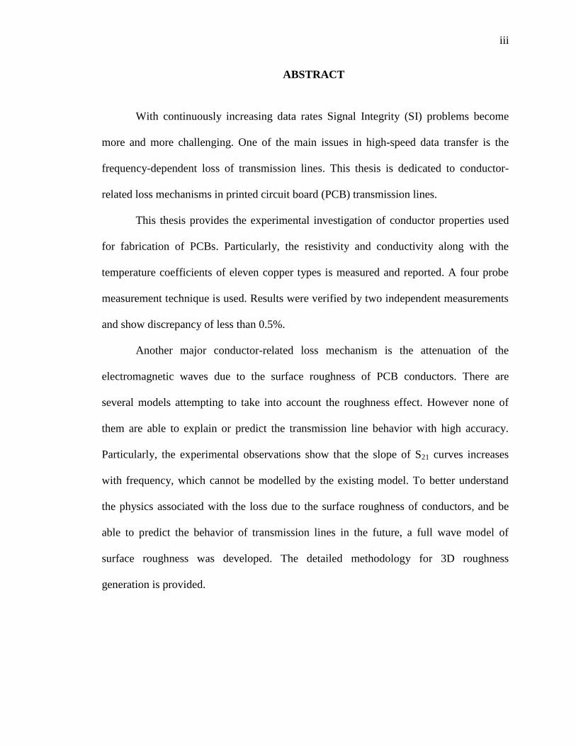

x
NOMENCLATURE
Symbol Description
E Electric field vector
E0 Electromagnetic wave amplitude
ω Angular frequency
119891 Frequency
k Wave number
120574 Propagation constant
120572 Total attenuation constant
120573 Phase constant
120572119888 Conductor loss
120572119889 Dielectric loss
120575 Skin depth
120590 Conductivity of metal
120583 Absolute permeability
ε Absolute permittivity
120588 Resistivity
ρ0 Resistivity at reference temperature
T0 Reference temperature
αT Temperature coefficient
ℎ119903119898119904 ldquoroot-mean-squaredrdquo (RMS) value of surface roughness magnitude
119869 Current density
xi
I Current
A Cross section area of the trace
119909120583 Mean value of sequence
R Resistance
S Standard deviation
∆119906 Standard uncertainty
∆120588 Uncertainty in resistivity
119870119904 Power loss coefficient
Atile Title area
119860119887119886119904119890 Base area of the hemispheres
W(kx ky) Power spectral frequency function
119897ACR Correlation length
Wn Normalized cut-off frequency
G Gain of the FIR filter
1 INTRODUCTION
The complexity of design and rapidly increasing data rate in high-speed digital
electronics makes the signal integrity performance hard to maintain As the data rate
increases the loss in transmission lines becomes the main issue for signals with clock
higher than 1GHz [1] As a signal propagates along a transmission line the frequency
dependent loss causes the signal degradation as the high-frequency part of the spectrum
experiences higher attenuation A transmission line with high loss causes more signal
distortion and limits the speed of the transmitted data This makes it important to
determine the high-frequency loss behavior in PCBs at the design stage
There are several mechanisms of loss in transmission lines but the primary ones
are conductor loss dielectric loss and loss due to the surface roughness of the traces [1]
Models of transmission lines need to take into account all three physical loss
mechanisms The conductor and dielectric loss are relatively well studied and good
models for them exist [2] In order to use these models the parameters of materials need
to be determined by measurement The conductor loss is equally important as the
dielectric loss but it is typical to use nominal value for the resistivity of copper to model
PCB transmission lines [1 2] In this work a practical and easy-to-implement method for
the conductor loss measurement (including temperature dependency) is presented The
obtained results indicate that the actual resistivity of copper used to create PCB
interconnects is noticeably lower than the nominal value and needs to be measured in
order to improve the accuracy of the transmission line modeling
Another very important factor determining the loss of PCB transmission lines is
the surface roughness of copper layers [3][4] Despite its importance there is still no
satisfactory understanding of physical mechanisms responsible for the roughness-related
attenuation and existing models do not provide enough accuracy in many cases as will be
shown further In this work a new full-wave model of conductor surface roughness is
proposed that can be used to investigate physical effect associated with conductor
surface roughness
2
11 CONDUCTOR ndash RELATED LOSS IN TRANSMISSION LINE
An electromagnetic wave propagating inside any real physical medium
experiences attenuation or in other words such medium has loss The attenuation is
characterized by attenuation constant and is related to the material properties of the
particular medium The electric field of the x-polarized TEM plane wave propagating
along z coordinate is [6]
119812(119911) = 1198640119890minus120574z119890ωt119857 (1)
where 1198640 is the wave amplitude ω is the angular frequency x is the unit vector in x
direction and 120574 is a propagation constant given as
120574 = 120572 + 119895120573 (2)
where 120572 is attenuation constant and 120573 is the phase constant which determines the wave
speed in medium it propagates in Usually waveguide structures consist of conductor and
dielectric both contributing to the attenuation constant In such structures the propagating
electromagnetic wave is attenuated mainly due to the conductor and dielectric loss but
other factors such as conductor surface roughness are also relevant [5] For low-loss
transmission lines it is possible to separate the total attenuation into a conductor loss and
dielectric loss components [1] [2]
120572 asymp 120572119888 + 120572119889 (3)
Conductor loss 120572119888 is related to the skin depth 120572119888 prop 1120575 which is defined as the
depth where the amplitude of the field vectors decays 119890 times In good conductor the skin
depth is [1][3]
120575 asymp radic1
119891120590120587120583 (4)
3
where f is the frequency σ is the electrical conductivity and micro is the permeability of the
conductor The electrical conductivity is reciprocal to the electrical resistivity 120590 = 1120588
and measures a materials ability to conduct an electric current
The skin effect describes the tendency of alternating current (AC) to flow near the
conductor surface The direct current (DC) distributes uniformly within the entire cross
section of the conductor and the resistive loss in this case relates to the cross-section area
of the conductor and metal conductivity but as the frequency increases the current begins
to flow in a thin layer beneath the surface of conductor approximately equal to the skin
depth The skin effect shrinks the effective cross-section of the conductor increasing the
resistance proportionally to radic119891 Therefore the conductor loss depends on the material
properties geometry of the conductor and is frequency-dependent
At the same time the resistivity of metals is temperature-dependent If the
temperature T changes within several hundred of K the temperature dependence of
electrical resistance is can be approximated by a linear function [7]
120588(119879) asymp 1205880[1 + 120572119879(119879 minus 1198790)] (5)
where 1205880 is the resistivity (in Ωm) at the reference temperature T0 and αT is the
temperature coefficient of resistivity (in minus1 or Kminus1)
Due to high current consumption the operating temperature of modern equipment
is typically considerably higher than room temperature [8] The temperature is high
enough to noticeably increase of resistivity and therefore the attenuation of the
transmission line The example of the increased loss due to temperature is shown on
Figure 11 Simulations were done for a 5000 mil long stripline structure having 3 mil
trace width and 91 mil thickness of the bulk dielectric Dielectric has the dielectric
constant (DK) of 4 and dissipation factor (DF) equal to 0008 (medium-loss dielectric)
Applying Eq4 and using 1205880 = 1724 ∙ 10minus8 Ωm (nominal value for pure copper)
120572119879 = 000393 1 1198790 = 25 the resistivity at 119879 = 25 and 119879 = 125 is
calculated After that the transmission coefficient of the line is calculated using the model
in Advanced Design System [45] The resulting coefficients are shown in Figure 11 As
4
can be seen increasing the temperature by 100 C leads to 1 dB difference at 50 GHz and
cannot be neglected in some cases
Figure11 Modeled transmission coefficients of stripline at 25 and 125
The purpose of Chapter 2 of the thesis is to study the temperature dependency of
resistance for different copper types used in PCB design
As was said above the conductor surface roughness is an important factor
affecting the performance of high-speed transmission lines Real PCB traces are not
smooth and the surface quality depends on technological process used during the PCB
fabrication [9] Also copper traces in transmission lines are intentionally made rough to
promote adhesion to the dielectric Typically ldquoroot-mean-squaredrdquo (RMS) value of
roughness is calculated as [10]
ℎ119903119898119904 = radicE [(119883 minus 119909120583)2
] (6)
where X is the profile function 119909120583 is the mean value of X and E denotes as expected
value operator
There are other parameters of surface roughness that can be found in literature
For example Rz referred to as ten point height is the average absolute value of the five
highest peaks and the five lowest valleys The ℎ119903119898119904 (or Rq in literature) typically is 025-
07μm for hyper very low profile (HVLP) foils 03-10μm for very low profile (VLP)
0 10 20 30 40 50-16
-14
-12
-10
-8
-6
-4
-2
0
Frequency (GHz)
|S21| d
B
T=125 C
T=25 C
5
foils and 10-20μm for standard profile (STD) foils [1 9 10 48] The examples of
several foil type profiles are presented in Figure 12
Figure 12 Optical microscopic images of roughness From left to right STD (standard)
VLP (very low profile) HVLP (hyper very low profile)
At frequencies starting from approximately 2GHz the skin depth becomes
comparable to the RMS height of the surface roughness impacting the flow of the current
considerably
Modern commercial software tools have models for conductor surface roughness
in transmission lines however all of them provide insufficient accuracy (in-depth review
of models is presented in Section 3) Examples are presented in Figure 13
Figure13 Hall Hemispherical model used in ADS [5] (a) GMS model developed in
Simberian Inc [11] (b)
In order to improve our understanding of the physical processes in striplines with
rough conductors a full-wave model is proposed in Section 3 It might be used in the
future as the basis of a truly physics-based roughness model
a b
6
2 MEASUREMENT OF COPPER RESISTIVITY
Pure copper has relatively low electrical resistivity among commercially useful
metals On the other hand the resistivity of different copper types used for PCB
fabrication might vary [12]What is worse is that thermal processing of copper (like
annealing) affects the resistivity profoundly [13] Because of this it becomes impossible
in many cases to predict the actual resistivity of conductors in PCBs
Resistivity is temperature dependent if the temperature increases resistivity
increases as well This chapter will outline the methodology for temperature dependence
measurements of the resistivity A quick explanation of four probe technique is provided
Then the methodology is applied to the eleven copper types used in PCB design The
resistivity and conductivity values as well as temperature coefficients are calculated and
discussed
21 BACKGROUND
Electrical resistivity of copper and its temperature dependence has been
investigated and reported by many groups over more than a century The earliest report is
published by Lorenz [14] in 1881 In his work he obtained the resistivity values of
218 ∙ 10minus8 Ωm and 295 ∙ 10minus8 Ωm at 273K and 373K correspondingly Next the
report of Jaeger and Diesselhorst [15] was published in 1900 where they performed
measurements at 291K and 373K and the reported resistivity is 181 ∙ 10minus8 Ωm
and 240 ∙ 10minus8 Ωm Referring to JH Dellinger [16] work published in 1900 the
reported temperature coefficient is 000394 but resistivity value is not provided In work
of Niccolai [17] made at 1908 the measurements were done from 84K to 673K with
reported changes in resistivity from 0302 ∙ 10minus8 Ωm to 4093 ∙ 10minus8 Ωm The 1914
report of Northrup [18] presents the data starting from room temperature to well above
the melting point In 1914 Stratton [19] published work with obtained resistivity value
and temperature coefficient Then in 1927 Gruneisen and Goens [20] did measurements
on numerous copper specimens from 212K to 273K In [21] Laubitz did the
measurements of the annealed 99999 pure copper from 273K to1272K Moore et al
measured the same samples Laubitz used but temperature was varied from 85K to 375K
There are numerous works by other authors dedicated to investigation of copper
7
resistivity under temperature influence Explicit data analysis was performed by Matula
in 1979 [7] In his work he consolidated all reported data related to resistivity of copper
and provided the recommended values at different temperatures which partly are given in
Table 21
Table 21 Values for the electrical resistivity and temperature coefficients of annealed
copper
The conductivity of a material is defined by differential form of Ohmrsquos law as
119869 = 120590119864 (7)
where J is the current density and Ε is the electric field in the direction of current flow It
is useful to express conductivity in terms of more familiar voltage and current The
current density is given by
119869 = 119868119860 (8)
where I is the current in Amperes and A is the cross sectional area of the conductor The
electric field is given
119864 = 119881119871 (9)
Author Temperature
K
Resistivity
Ωm
Temp
Coefficient
1
Matula 30027 1725 ∙ 10minus8
NA 35077 2063 ∙ 10minus8
Dellinger 29320 NA 000394
Stratton 29320 1724 ∙ 10minus8 000393
8
where V is the total voltage drop along the conductor sample and L is the length of the
sample Rearranging (7) and substituting to (8) and (9) gives
120588 =1
120590=
119864
119869=
119860∙119881
119871∙119868=
119877∙119860
119871 (10)
where ρ is the sample resistivity (in Ωmiddotm) and R is the samplersquos measurable resistance (in
Ω) Thus by measuring the resistance directly (or the voltage and current) and knowing
the samplersquos physical dimensions the resistivity or its conductivity can be calculated
211 Four-Probe Technique For the resistance measurements of the conductors
the four probe technique is typically used [22][23] The schematic of the four probe
technique is shown in Figure 21 It consists of the current source ampere-meter and
voltmeter Connection of the current source and voltmeter to the sample is performed
using the probes Then current I is made to flow between the probes as shown by red
arrows in Figure 21 Voltage V is measured between the two probes ideally without
drawing any current and avoiding the resistance error factor (including contact
resistance) From the ratio of measured voltage and current the resistance can be
determined using the Ohm law
Figure 21 Schematic of Four - Point Probe Technique
9
212 Setup For the Resistance measurements the LCR meter HP4263b with
custom probes is used Probes are made using pogo pins and coax cables and are shown
in Figure 22 The LCR meter is the instrument which is usually used for inductance (L)
capacitance (C) and resistance (R) measurements It has four terminals two can measure
voltage across the sample and another two apply current to the sample according to the
diagram in Figure 21 Although the measurements are performed at 100 Hz the skin
effect at this frequency is negligible and the results are indistinguishable from the
measurements at DC
Figure 22 Pogo pin (left) Customized probes for resistivity measurements (right)
For the temperature dependence measurements the device under test (DUT) must
be heated up for as long as the measurement requires To heat up the DUT the hot plate
with the adjustable temperature is used The temperature range of interest is from room
temperature 25degC (298 K) to 100degC (373K)Two thermocouples are connected to the
DUT to monitor the temperature and two precision digital thermometers (ΔT=01 K) are
used to read the temperature from thermocouples The schematic of the setup is shown in
Figure 23
pogo pin Probes
10
Figure 23 Setup schematic for resistance measurements
The main problem is to maintain the homogeneous temperature distribution over
the hot plate Requirement for this study is that the discrepancy of temperature should not
exceed 1degC In order to meet it the DUT is put between two metal plates The bottom
plate has around 10 mm thickness and the top plate is 2 mm thick and has thermal Mylar
tape on it to avoid shorting the sample The bottom plate is then heated by the hot plate
and the top one helps to keep the DUT temperature steady The setup implementation is
presented in Figure 24 The ldquosandwichrdquo structure provides the homogenous temperature
distribution over the entire DUT needed for this study To be able to land the probes and
perform the measurement the 15x15 cm window is cut in the top plate Provided space
is enough to land four probes connected to the LCR Meter Window of this size does not
affect the accuracy of the measurement because the rest of the DUT stays covered and the
bottom plate has not been changed
11
Figure 24 Setup for resistance measurements (a) window for probes landing (b) two
thermocouples placed on the DUT (c)
To summarize the procedure for temperature dependency investigation the
following steps should be taken
Put the DUT between two plates and start heating
Monitor the temperature until it reaches the desired one
Take Resistance measurements applying four probes of the LCR Meter
Two thermocouples
LCR Meter
Digital thermometers
Window for
measurements
a
b c
12
213 DUT Description For the temperature dependency investigation the set
of copper coupons has been fabricated The top layer of coupon is presented in Figure
25 The bottom layer of all coupons is solid copper Totally eleven copper types have
been provided for this study Every copper type contains 30 coupons and every ten of
them have different trace width The specific copper types will be listed latter
The length of each sample is 1 m As it is shown in Figure 25 each sample has
special form to minimize the occupied space and to put the sample ends close to each
other
The main feature of these coupons is a 05 mm gap to be able to place probes for
measurements
Figure 25 Top layer of tested coupon
Another parameter needed for resistivity calculation is a cross sectional area The
cross section is taken by cutting the sample by the plane normal to the current flow For
accurate calculation several traces were cut polished and measured using an optical
microscope One of the cross sections with measured thickness is presented in Figure 26
Gap
13
Figure 26 The cross section of the tested trace
214 Uncertainty Estimation The usual way to quantify the spread of
measured data is standard deviation The standard deviation of a set of numbers tells how
different the individual readings typically are from the average of the set The bias-
corrected standard deviation for a series of n measurements can be expressed
mathematically as
119878 = radicsum (119909119894minus)2119899
119894=1
119899minus1 (11)
where is the arithmetic mean of measured data When a set of several repeated readings
has been taken the uncertainties should be properly estimated All contributing
uncertainties should be expressed at the same confidence level by converting them into
standard uncertainties Standard uncertainty Δu (or Standard Error (SE)) is determined as
the standard deviation of the mean [24] and calculated as [24-28]
∆119906 =119878
radic119899 (12)
This expression reflects the fact that standard uncertainty decreases with
increasing the number of measurements
14
Oftentimes the uncertainty should be calculated for quantity f which depends on
several variables 119909119894 with their own uncertainties In this case the uncertainty in f is
determined as [24-28]
∆119906119891 = radicsum (120597119891(119909119894)
120597119909119894∆119906(119909119894))
2119873119894=1 (13)
Consider the Cross sectional area of the trace given by
119860 = 119882 ∙ 119879 (14)
where W is the trace width and T is its thickness Then applying (13) the uncertainty in
the area is given by
∆119860 = (119882 ∙ 119879)radic(∆119882
119882)
2+ (
∆119879
119879)
2 (15)
where the width uncertainty ∆119882 and thickness uncertainty ∆119879 are calculated using (11)
W and T are the mean values calculated from microscopic photos The calculated area
and its uncertainties are consolidated in Table 22
Table 22 Thickness width and area of traces
Thickness μm 1802plusmn015
Width μm 48824plusmn059 49362plusmn120 49900plusmn060
Area μm2 879808plusmn7399 887701plusmn7677 899198plusmn7541
Considering the relative uncertainties of width ∆W
119882=
059
48824= 12 lowast 10minus3 =
012 thickness ∆T
119879=
067
1802= 83 lowast 10minus3 = 083 and calculated area
∆A
119860=
7399
879808=
15
084 it is obvious that the thickness has the dominating contribution to the total
uncertainty
The uncertainty in resistivity can be derived by substituting (10) to (13)
∆120588 = radic(119860
119871∙ ∆119877)
2+ (
119877
119871∙ ∆119860)
2+ (minus
119877119860
1198712 ∙ ∆119871)2 (16)
Equation (16) shows that the total uncertainty of resistivity depends on the
corresponding uncertainties of area sample length and measured resistance The
uncertainty related to sample length is not considered and neglected The uncertainty in
resistance depends on particular setup and measurement method and was 01 according
to the LCR meter specification There are several other type of errors such as systematic
ones Only random errors are considered in this work
215 Results and Discussion Measurements of resistance were done using
LCR meter HP4263b for 330 samples (11 foil types by 30 samples) at room temperature
(25 degC) 50 degC and 100 ˚C Applying (10) the resistivity and conductivity values have
been calculated and presented in Tables 24-25 Results were confirmed by
measurements in the Material Research Center (MRC) at room temperature using
another much more expensive facility (Allesi C4S) based on the same 4-point technique
Picture of Allesi C4S instrument is presented in Figure 27 Discrepancy in resistivity
obtained by two independent measurements (LCR meter at AC and Allesi C4S at DC)
does not exceed 05 and is presented in Table 23 The measurements at 50 degC and 100
degC have not been verified due to Allesi C4S limitations Nevertheless such low
difference in results indicates that the instrument error has low contribution into total
uncertainty of calculated resistivity value
The results show that the conductivity values at room temperature of different
copper types are 125 lower on average than the nominal pure copper value σ = 580 ∙
107 Sm For convenience the obtained results are presented also in Figure 28 and Figure
29
16
Figure 27 Allesi C4S 4-point probe
Table 23 Comparison of conductivity obtained by two methods
(3 copper types are shown)
typesetup Allesi
Conductivity Sm
LCR Meter
Conductivity Sm
OM ML 4876 ∙ 107plusmn0044 ∙ 107 4873 ∙ 107plusmn0042 ∙ 107
OM MLS 5141 ∙ 107plusmn0046 ∙ 107 5153 ∙ 107plusmn0045 ∙ 107
NY NPV 4955 ∙ 107plusmn0057 ∙ 107 4931 ∙ 107plusmn0051 ∙ 107
Allesi C4S
Voltmeter
Current source
17
Table 24 Conductivity at room temperature 50 C and 100 C
type 120590 119878119898
at Room Temperature
120590 119878119898
At 50 C
120590 119878119898
At 100 C
OM ML 4873 ∙ 107plusmn0042 ∙ 107 4441 ∙ 107plusmn0038 ∙ 107 3730 ∙ 107plusmn0033 ∙ 107
OM MLS 5153 ∙ 107plusmn0045 ∙ 107 4687 ∙ 107plusmn0041 ∙ 107 3963 ∙ 107plusmn0037 ∙ 107
OM VSP 4984 ∙ 107plusmn0042 ∙ 107 4513 ∙ 107plusmn0039 ∙ 107 3804 ∙ 107plusmn0032 ∙ 107
NY NPHD 5073 ∙ 107plusmn0044 ∙ 107 4586 ∙ 107plusmn0039 ∙ 107 3874 ∙ 107plusmn0034 ∙ 107
NY NPV 4931 ∙ 107plusmn0051 ∙ 107 4471 ∙ 107plusmn0045 ∙ 107 3777 ∙ 107plusmn0037 ∙ 107
CF TW-B 5152 ∙ 107plusmn0044 ∙ 107 4696 ∙ 107plusmn0041 ∙ 107 3947 ∙ 107plusmn0035 ∙ 107
OM VLP 4809 ∙ 107plusmn0041 ∙ 107 4368 ∙ 107plusmn0038 ∙ 107 3694 ∙ 107plusmn0032 ∙ 107
CF BF-TZA 4780 ∙ 107plusmn0042 ∙ 107 4350 ∙ 107plusmn0039 ∙ 107 3687 ∙ 107plusmn0035 ∙ 107
FUR FV-WS 4840 ∙ 107plusmn0042 ∙ 107 4398 ∙ 107plusmn0038 ∙ 107 3722 ∙ 107plusmn0032 ∙ 107
GD RTC 5130 ∙ 107plusmn0044 ∙ 107 4662 ∙ 107plusmn0041 ∙ 107 3916 ∙ 107plusmn0038 ∙ 107
CF TW 5111 ∙ 107plusmn0046 ∙ 107 4644 ∙ 107plusmn0042 ∙ 107 3913 ∙ 107plusmn0035 ∙ 107
18
Table 25 Resistivity at room temperature 50 C and 100 C
type 120588 Ω ∙ 119898
at Room Temperature
120588 Ω ∙ 119898
At 50 C
120588 Ω ∙ 119898
At 100 C
OM ML 2053 ∙ 10minus8plusmn0017 ∙ 10minus8 2252 ∙ 10minus8plusmn0019 ∙ 10minus8 2681 ∙ 10minus8plusmn0024 ∙ 10minus8
OM MLS 1944 ∙ 10minus8plusmn0017 ∙ 10minus8 2134 ∙ 10minus8plusmn0019 ∙ 10minus8 2524 ∙ 10minus8plusmn0024 ∙ 10minus8
OM VSP 2007 ∙ 10minus8plusmn0017 ∙ 10minus8 2216 ∙ 10minus8plusmn0019 ∙ 10minus8 2629 ∙ 10minus8plusmn0022 ∙ 10minus8
NY NPHD 1972 ∙ 10minus8plusmn0017 ∙ 10minus8 2181 ∙ 10minus8plusmn0019 ∙ 10minus8 2581 ∙ 10minus8plusmn0023 ∙ 10minus8
NY NPV 2029 ∙ 10minus8plusmn0021 ∙ 10minus8 2237 ∙ 10minus8plusmn0022 ∙ 10minus8 2647 ∙ 10minus8plusmn0026 ∙ 10minus8
CF TW-B 1943 ∙ 10minus8plusmn0017 ∙ 10minus8 2129 ∙ 10minus8plusmn0019 ∙ 10minus8 2534 ∙ 10minus8plusmn0022 ∙ 10minus8
OM VLP 2081 ∙ 10minus8plusmn0018 ∙ 10minus8 2289 ∙ 10minus8plusmn0020 ∙ 10minus8 2707 ∙ 10minus8plusmn0024 ∙ 10minus8
CF BF-TZA 2094 ∙ 10minus8plusmn0018 ∙ 10minus8 2299 ∙ 10minus8plusmn0021 ∙ 10minus8 2712 ∙ 10minus8plusmn0026 ∙ 10minus8
FUR FV-WS 2064 ∙ 10minus8plusmn0018 ∙ 10minus8 2274 ∙ 10minus8plusmn0020 ∙ 10minus8 2687 ∙ 10minus8plusmn0027 ∙ 10minus8
GD RTC 1963 ∙ 10minus8plusmn0017 ∙ 10minus8 2145 ∙ 10minus8plusmn0019 ∙ 10minus8 2553 ∙ 10minus8plusmn0026 ∙ 10minus8
CF TW 1958 ∙ 10minus8plusmn0018 ∙ 10minus8 2153 ∙ 10minus8plusmn0019 ∙ 10minus8 2556 ∙ 10minus8plusmn0023 ∙ 10minus8
19
Figure 28 Conductivity over temperature for all tested copper types
Figure 29 Resistivity over temperature for all tested copper types
The temperature coefficients were calculated by inverting the equation (5) and
fitting resistivity values between 25 C and 100 C by a linear function The calculated
(fitted) resistivity temperature dependency is plotted in Figure 210 along with the
measured one
20 40 60 80 100
35
4
45
5
x 107
Temperature Co
Co
nd
ucti
vty
S
m
Room Temperature
T=50Co
T=100Co
20 40 60 80 100
19
2
21
22
23
24
25
26
27
x 10-8
Temperature Co
Resis
tivit
y O
hm
m
Room Temperature
50Co
100Co
20
Figure 210 Resistivity vs temperature
Performing the calculation for every measured copper type the temperature
coefficients have been extracted and presented in Table 26
Table 26 Temperature coefficients for tested copper foils
30 40 50 60 70 80 90 100
19
2
21
22
23
24
25
x 10-8
Temepature oC
Re
sis
tiv
ity
O
hm
m
measured
calculated
foil type temperature
coefficient1 Foil type
temperature
coefficient1
OM ML 407 ∙ 10minus3 OM VLP 400 ∙ 10minus3
OM MLS 397 ∙ 10minus3 CF BF-TZA 395 ∙ 10minus3
OM VSP 413 ∙ 10minus3 FUR FV-WS 402 ∙ 10minus3
NY NPHD 412 ∙ 10minus3 GD RTC 400 ∙ 10minus3
NY NPV 410 ∙ 10minus3 CF TW 406 ∙ 10minus3
CF TW-B 405 ∙ 10minus3
21
22 SUMMARY
The LCR Meter with custom probes can be used for the efficient and accurate
measurements of copper resistivity Resistivity values calculated based on LCR meter
measurements converge to those calculated based on measurements taken at the Material
Research Center using Allesi C4S at room temperature Calculated conductivity values at
room temperature of different copper types are 125 lower on average than the nominal
pure copper value σ = 580 ∙ 107 Sm
Further application of Allesi C4S for the temperature dependency measurements
is not possible due to its configuration For this purpose the LCR meter was successfully
utilized at 50 degC and 100degC providing expected linear behavior for resistivity Setup for
these measurements is easy to implement and does not requires using the environmental
chamber achieving the temperature discrepancy below 1 degC Resistivity values of tested
copper types show approximately linear behavior in 25-100 C temperature range
Overall the conductivityresistivity values change with temperature and average
difference between room temperature and 100C is 30 Calculated temperature
coefficients have good agreements with results presented in [8] Particularly the reported
temperature coefficients are in the range form 369 ∙ 10minus3 1C to 409 ∙ 10minus3 1C at
20C and the measured results are in the range from 395 ∙ 10minus3 1C to 413 ∙ 10minus3 1C
Also performed uncertainty estimation shows that the main contribution into the total
error is due to the uncertainty in the trace thickness In order to reduce the error the
actual area of tested samples has to be extracted from the microscopic images of the trace
cross section
22
3 SURFACE ROUGHNESS MODELING
In real PCBs the traces are never smooth and have rough surface causing the
additional loss [29-31] Moreover loss related to surface roughness increases with
frequency and affects the SI performance Since the clock frequencies of modern high
speed devices are in the multi-GHz region the effect of surface roughness cannot be
neglected in general
31 EXPERIMENTAL INVESTIGATION OF SURFACE ROUGHNESS
EFFECTS
For the experimental investigation of the influence of the surface roughness on
losses the set of PCB has been manufactured with different widths and foil types Totally
12 PCB sets were fabricated with every set consisting of six identical PCBs All test lines
are 50 Ohm single ended (SE) striplines and the Megtron6 is used as laminate dielectric
The picture of a typical test vehicle is given in Figure 31 The test board has a ldquothrough-
reflect-linerdquo (TRL) calibration pattern the valid frequency range of the calibration pattern
is at least up to 30 GHz
Figure 31 Picture of the test vehicle
The launch structure is a surface pad designed to accept a flange-mount
compression-fit SMA connectors The 35 mm SMA connectors are mounted on top of
the PCB and are used for excitation The drawing of the SMA connector is presented on
Figure 32
23
Figure 32 Drawing of SMA connector
Three foil types have been implemented for this research Standard foil (STD)
very low profile (VLP) and hyper low profile (HVLP) Roughness parameters for each
of them are provided in Table 31
Table 31 Roughness parameters for three tested foil types [47]
311 Measurement Results and Observations After the TRL calibration the
S-parameters of the 16 inch test lines on all PCBs have been measured Measured
insertion loss of 12 PCBs with different roughness and trace width are illustrated by
Figure 33
Resist Side ℎ119903119898119904 μm Peak to Peak μm
STD 10-20 70-120
VLP 03-04 30-40
HVLP 025-035 20-30
After alt Oxide ℎ119903119898119904 μm Peak to Peak μm
STD 10-20 70-120
VLP 06-10 60-80
HVLP 05-07 40-60
24
Figure 33 |S21| per inch for the entire PCBs set
The obtained results show that first of all the insertion loss increases with the
magnitude of roughness as expected also the additional loss due to the roughness
increases with frequency At the same time the impact of the surface roughness on the
total loss decreases for wider traces The difference in losses with respect to HVLP at
15GHz are given in Table 32 illustrating these effects
Table 32 Difference in loss for different trace width at 15GHz
35mil 95mil 13mil 15mil
STD-HVLP 378 239 377 168
VLP-HVLP 118 88 86 64
0 5 10 15 20 25 30-16
-14
-12
-1
-08
-06
-04
-02
0
Frequency (GHz)
|S21| d
Bin
ch
w95mil HVLP
w95mil RTF
w95mil STD
0 5 10 15 20 25 30-3
-25
-2
-15
-1
-05
0
Frequency (GHz)
|S21| d
Bin
ch
w35mil HVLP
w35mil RTF
w35mil STD
0 5 10 15 20 25 30-14
-12
-1
-08
-06
-04
-02
0
Frequency (GHz)
|S21| d
Bin
ch
w15mil HVLP
w15mil RTF
w15mil STD
0 5 10 15 20 25 30-16
-14
-12
-1
-08
-06
-04
-02
0
Frequency (GHz)
|S21| d
Bin
ch
w13mil HVLP
w13mil STD
w13mil VLP
25
Another unexpected observation is that the slope of S21 curve increases with
frequency which is particularly visible for HVLP traces
Attenuation coefficient due to the dielectric loss is proportional to the frequency
as 120572119889 = 119862 ∙ 120596 ∙ tan120575 where C is the per unit length (pul) capacitance of the line [6] Since
the conductor loss increases proportionally to the radic120596 (see [1]) at sufficiently high
frequencies the dielectric loss dominates and one should expect almost linear increase of
loss factor for non-dispersive dielectrics The measurements in Figure 33 however show
noticeably non-linear behavior at high frequencies This behavior was observed in other
research groups independently for example as it is shown in Figure 34
Figure 34 Nonlinear behavior of the insertion loss due to the surface roughness [29]
In principle the increase of the slope of S21 could be explained by the frequency-
dependent loss in the dielectric in the multi-GHz frequency range (as is done in [32])
however on the other hand there are reports indicating that the low-loss dielectrics
typically used in the PCB design are very low-dispersive above 5 GHz and have nearly
frequency independent tanδ (examples are presented in Figure 35 (resonator method) and
Roughness increases HVLP
to STD
26
Figure 36 (transmission line method)) [3348] If it is true the non-linearity of the
attenuation constant must be attributed solely to the effects of conductor surface
roughness
Figure 35 Measured of the real and imaginary components of Roger 5880 [33]
Figure 36 DK DF of bismaleimide triazine (BT) [47]
101
102
0
02
04
06
08
1
Frequency GHz
27
312 Motivation and Objective Generally these observed effects could not be
explained by any existing models as will be demonstrated in the following section and
calls for the development of the alternative approach Ideally this approach needs to be
physics-based as opposed to phenomenological or behavior modelling A truly physical
approach should involve direct solutions of Maxwellrsquos equations which might be
achieved using one of the commercially available full-wave solvers There are several
challenges that are met when the rough surface is modelled in 3D The obvious one is
that the mesh density (or the number of unknowns) needed to describe the rough surface
of a typical PCB conductor is quite high and might be prohibitive for certain types of
solvers Secondly the high-frequency 3D solvers do not mesh the inner volume of metal
parts but use boundary conditions to model lossy metals instead However the
penetration of field into the metal might be comparable to the size of metal protrusions
due to the roughness and boundary conditions might be not adequate in this situation
And thirdly there are complex chemical compounds that are formed at the interface
between the dielectric and metal [34] which might have quite distinctive electrical
properties Currently there is no way to include the effect of these compounds into the 3D
model because their properties and the thickness of the layer generally are not known
Nevertheless despite these challenges and limitations it was decided to
investigate the possibility to model the rough surfaces of the striplines in full-wave
primarily to get insights into the physics of the roughness-related attenuation
32 EXISTING MODELS FOR SURFACE ROUGHNESS
Many models for conductor surface roughness are based on representation of
roughness profiles by simple shapes In some models the shapes are placed periodically
to simplify the analysis in others the stochastic methods are employed
The usual way to estimate the loss due to rough surface is to calculate the
correction factor or power loss coefficient The power loss coefficient is equal to the ratio
of the attenuation constant due to conductor loses of a transmission line with rough
conductor surfaces to that for the same line with smooth conductor surfaces
321 Hammerstad Model The first model to account for the surface
roughness losses was proposed by Morgan in 1949 [35] In his model the roughness is
28
presented as periodic ldquosaw toothrdquo like structure as shown on Figure 37 The assumption
behind this theory is that current flows along the edge of the rough surface as it is show
on the figure and the additional power losses caused by longer current path Then he used
the finite-difference method to solve a quasi-static eddy-current problem for this
structure As the result the ratio of the power loss dissipated in a conductor with a rough
surface 120630119955119952119958119944119945 to that dissipated in the same but smooth conductor 120630119956119950119952119952119957119945 is calculated
Figure 37 Hammersted model for roughness modeling
Later Hammerstad and Jensen obtained the empirical expression based on
Morganrsquos results for extra loss and used only one parameter hrms to characterize it [3]
119870119904 =120572119903119900119906119892ℎ
120572119904119898119900119900119905ℎ= 1 +
2
120587∙ 119886119903119888119905119886119899 (14 (
ℎ119903119898119904
120575)
2
) (17)
where 120575 is the skin depth However obtained expression saturates at the value of 2 as it is
shown in Figure 38 for ℎ119903119898119904 = 58119906119898
29
Figure 38 Roughness correction factor based on Hammersted model
In practice the impact of surface roughness can be greater than a factor of 2
which leads to lack of accuracy at high frequencies The example of loss correction using
this method is shown in Figure 39
Figure 39 Measured and corrected according to Hammersted insertion loss [5]
As it is well seen the application of Hammersted model is limited to 4-5GHz
where it has reasonable accuracy While this model has been found useful in low
frequency speed designs the modern high-speed circuits require more accurate models
0 10 20 30 40 501
15
2
25
Frequency (GHz)
Co
rre
cti
on
fa
cto
r K
30
322 Hemispherical Model Hall et al proposed to model the conductor
surface roughness as conductor hemispheres protruding from a at conductor plane [5]
Then the problem of scattering of a plane wave from the hemispherical protrusion on the
flat surface is solved using the method of images The correction factor is given then as
119870119904 =(|119877119890[120578
3120587
41198962(120572(1)+120573(1))]|+1205830120596120575
4(119860119905119894119897119890minus119860119887119886119904119890))
1205830120596120575
4119860119905119894119897119890
(18)
where 119860119905119894119897119890 is the tile area 119860119887119886119904119890 is the base area of the hemispheres k is wave vector
120578 = radic1205830휀0휀prime and the first order scattering coefficients are
120572(1) = minus2119895
3(119896119903)3 [
1minus120575
119903(1+119895)
1+120575
2119903(1+119895)
] (19)
120573(1) = minus2119895
3(119896119903)3 [
1minus(4119895
1198962119903120575)(
1
1minus119895)
1+(2119895
1198962119903120575)(
1
1minus119895)] (20)
The parameters for 119870119904 are calculated based on volume equivalent model as
119860119905119894119897119890 = 1198891199011198901198861198961199042 (21)
119860119887119886119904119890 = 120587 (119887119887119886119904119890
2)
2
(22)
119903 = radicℎtooth (119887base
2)
23
(23)
The meaning of these parameters is illustrated by Figure 310
31
Figure 310 Hemispherical model for roughness modeling
An example of applying Eq(18) with roughness parameters 119887119887119886119904119890 = 94119906119898
119889119901119890119886119896119904 = 94119906119898 휀prime = 4 the correction coefficient in 0 to 50 GHz frequency range is
presented in Figure 311
Figure 311 Roughness correction factor based on Hemispherical model
Application of this model gives relatively accurate results up to 30 GHz [5] as it is
shown on Figure 312
0 10 20 30 40 501
15
2
25
3
Frequency (GHz)
Co
rre
cti
on
fa
cto
r K
32
Figure 312 Measured and corrected according to Hall insertion loss [5]
Hemispherical model is the most popular today and found implementation in
commercial software It is based on three input parameters and requires three statistical
measurements However the accurate measurements of base and space between
protrusions are required On the other hand as can be seen in Figure 312 the model
typically overestimates loss at low frequencies and underestimates at high ones And as
the frequency increases past 30 GHz the underestimation of loss increases
323 Snowball Model In the work of Huray et al the surface roughness is
modeled as a pyramidal stack-up of spherical conductor particles snowballs on a
conductor surface [36-37] as shown in Figure 313
Figure 313 Snowballs model for roughness modeling [36]
33
The problem of scattering and absorption is solved similarly to the hemispherical
model but for every sphere Using the superposition of the sphere losses the total loss of
this structure is derived As the result the roughness correction factor is written as
119870119904 =1205830120596120575
4119860119905119894119897119890+sum 119877119890[120578
3120587
21198962(120572(1)+120573(1))]119873119899=1
1205830120596120575
4119860119905119894119897119890
(24)
Calculated roughness correction factor is presented on Figure 314 Roughness
parameters in this example were the same as in previous model and radii of spheres are
08μm Total number of spheres is N=20
Figure 314 Roughness correction factor based on Snowballs model
This model shows the accurate agreement with measurements up to 50GHz but is
complicate to use The application of this model is shown on Figure 315
0 10 20 30 40 501
15
2
25
3
Frequency (GHz)
Co
rre
cti
on
fa
cto
r K
34
Figure 315 Measured and corrected according to Snowball model insertion loss [5]
As can be seen the agreement at lower frequencies is better but the model also
underestimates loss at higher frequency range
324 Small Perturbation Method Tsang et al conducted more complicated
and deep analysis of the surface roughness problem [38-42] Firstly they analyzed 2D
random rough surfaces based on second order Small Perturbation Method (SPM2) and
numerical method of moments (MoM) [42] Then they performed calculation of power
absorption factor for surface roughness with Gaussian and Exponential correlation
functions Calculations and analysis show that the power absorption enhancement factor
depends on three parameters RMS height correlation length and correlation function
Then this approach has been extended to the analysis of 3D surface roughness
where the surface height varies in both horizontal directions [38] In this work authors
derived the closed-form formula of the power absorption enhancement factor based
119870119904 = 1 +2ℎ2
1205752minus
4
120575int int 119889119896119909119889119896119910119882(119896119909 119896119910)119877119890 radic
2119894
1205752minus 119896119909
2 minus 1198961199102
infin
0
infin
0 (25)
where 119896119909119910 =2120587119899
119871119909119910 and 119882(119896119909 119896119910) is the power spectral density function (PSD)
The example of correction factor calculated using equation (25) is presented on
Figure 316 Calculation was made for roughness profile havingℎ119903119898119904 = 1 119906119898 correlation
length 2 μm and Gaussian function of PSD
35
Figure 316 Roughness correction factor based on SPM2
The comparison of measured and estimated loss show accurate prediction up to 20
GHz and is presented in Figure 317 [39] However this method has been tested only for
ℎ119903119898119904 le 1119906119898 and gives unrealistic correction factor for higher roughness magnitude
Figure 317 Measured and modeled according to SPM2 [39]
0 10 20 30 40 501
11
12
13
14
15
16
17
18
Frequency (GHz)
Co
rre
cti
on
fa
cto
r K
36
325 Scalar Wave Modeling Another model based on the stochastic analysis
is proposed in the work of Chen and Wong In their work [43] the rough surface is
modeled by parameterized stochastic processes The method is based on 3D statistical
modeling of surface roughness and the numerical solution of scalar wave equation The
extra loss caused by surface roughness is approximated by the energy flux absorbed by
the rough surface The scalar wave modeling (SWM) with the method of moments
(MOM) is used to calculate the scattering and absorption of the scalar wave by the rough
surface As the validation of this method the comparison with the SPM2 method was
performed (Figure 318) but not with the experimental results
Figure 318 Roughness correction factor calculated by SWM vs SPM2 [43]
Despite the reported advantages of SWM method it was derived based on scalar
wave theory instead of EM wave theory
326 Limitations of Existing Models As can be seen all of the models
reviewed above improve the accuracy of modelling relative to the case when the surface
roughness is not taken into account The accuracy of prediction is different being the
worst for the Hammersted model and the best for the snowball model However none of
the existing models is capable to capture the effect of increasing slope of the S21 due to
37
the roughness that is evident from Figure 33 and 34 as the correction factors calculated
according to all of them have monotonic second derivative (see Figure 38 311 314
316 318) The slope increase effect can be quite strong adding up to 5 dB loss at 10
GHz (see Figure 34) and definitely requires a closer attention
33 3D MODEL FOR SURFACE ROUGHNESS
The paper [43] proposes the way to generate a surface resembling the real-word
profiles of rough conductors based on the cross-sectional measurements We will follow
a similar procedure to generate the surfaces that can be automatically imported into CST
Microwave Studio
To generate the random roughness the following steps should be taken
Explore the parameters of real roughness Extract statistical parameters
such as probability density function (PDF) Autocorrelation function
(ACR) and ℎ119903119898119904 from the measured roughness profile
Generate the δ-correlated 2D function (surface) with needed PDF
Design a filter and filter the δ-correlated function to obtain a surface with
needed ACR
Import generated surface into CST Microwave studio and perform full
wave simulation
331 Extraction of Roughness Parameters For the surface roughness
characterization the cross section-analysis is essential To perform the cross-sectional
analysis the trace is cut perpendicular to wave propagation direction For this study
several PCB with different foil types have been cut embedded into a special epoxy
compound polished and the microscopic images of the cross-sections are taken Prepared
samples and microscopic images are presented in Figure 319
38
Figure 319 Prepared sample for cross section analysis (a) microscopic pictures of
stripline (b) close-up picture of the trace (c)
The procedure of image processing for PCB cross section analysis is described in
details in [10] After image processing the binary (black-and white) image of the cross-
section is generated The example of the binary image of the VLP trace is shown in
Figure 320
Figure 320 Binary image of the cross-section for VLP
a
b c
10 m
39
The surface roughness profile is extracted directly from the binary images
Roughness profile of the top surface in Figure 320 is shown in Figure 321 and its
autocorrelation function is in Figure 322 The histogram of the profile is presented in
Figure 322
Figure 321 Extracted roughness profile of VLP foil (oxide side)
Figure 322 Autocorrelation function of the VLP foil roughness profile Correlation
length is indicated by the marker
0 10 20 30 40 50 60 70
-2
-15
-1
-05
0
05
1
15
2
xum
Mag
nit
ud
eu
m
-50 0 50
-2
-1
0
1
2
3
4
5
x 104
xum
AC
R
-4 -2 0 2 4
1
15
2
25
3
35
4
45
5
55
x 104
X 1306
Y 2119e+004
xum
AC
R
40
Figure 323 Histogram of VLP foil
The correlation length lACR is defined as the distance where the magnitude of the
autocorrelation function decreases e times and is equal to 13μm in the case on Figure
322 The correlation length can be used to determine the required discretization step as
will be shown later Measured rms height (according to (6)) of the profile is ℎ119903119898119904=081
μm To completely characterize a random function (or a signal) the Probability Density
Function (PDF) is needed however the accurate extraction of it is not possible (as can be
seen in Figure 323) due to limited number of data samples and the normal distribution
was assumed
332 Generation of the 3D Surface In order to create a random surface
firstly a 2D array filled with δ-correlated random numbers is generated The numbers
have normal distribution with zero mean and standard deviation of 1 The adjustment of
the correlation length is achieved by filtering the array by a 2D filter
Generally the filter might be of any kind if it has a needed frequency response
For instance in [43] a Gaussian 2D filter is used However we use 2D finite impulse
response (FIR) low pass filter for simplicity of implementation For the FIR filter of
order N each value of the output sequence 119910[119899] is a weighted sum of the most recent
input values and is given as
-25 -2 -15 -1 -05 0 05 1 15 2 250
200
400
600
800
1000
1200
xum
41
119910[119899] = 1198870119909[119899] + 1198871119909[119899 minus 1] + ⋯ + 119887119873119909[119899 minus 119873] (26)
The internal Matlab function fir1(NWn) is used to generate the 1D prototype
filter Wn is the normalized cut-off frequency which can vary between 0 and 1 where 1
corresponds to the Nyquist frequency Frequency response of such a filter is presented in
Figure 324 for Wn=01 and N=4
Figure 324 Frequency response of a 1D FIR prototype filter
After the 1D prototype filter is generated by the fir1 functions the Matlab
function ftrans2(b) is used to produce the two-dimensional FIR filter that corresponds to
the one-dimensional FIR filter
Examples of frequency response of 2D FIR filters are presented in Figure 325 for
N=4 Wn=01 and N=4 Wn=08
0 02 04 06 08 10
02
04
06
08
1
Normalized Frequency (piradsample)
Ma
gn
itu
ge
42
Figure 325 Frequency responses for Wn=01 (right) and Wn=08 (left) N=4 in both
cases
The gain of the filter produced by the ftrans2 function is 1 at zero frequency In
order to obtain the output array with the desired ℎ119903119898119904 the output of the filter is
multiplied by the gain constant G which is tuned
Then filtering of 2D δ-correlated array by the 2D FIR filter with the frequency
response 119867(1205961 1205962) and multiplication by G gives the final rough surface with
needed ℎ119903119898119904 correlation length and PDF
Described technique provides opportunity to generate surface of any size and
imports it into commercial solvers (technical difficulties of importing are discussed
below) The example of generated surface and realistic surface measured by profilometry
is presented in Figure 326
-1
-05
0
05
1
-1
-05
0
05
10
02
04
06
08
1
Fx
Fy
Magnitude
-1
-05
0
05
1
-1
-05
0
05
104
05
06
07
08
09
1
Fx
Fy
Magnitude
43
Figure 326 Surface roughness profile measured by a profilometer [5] (left) and
generated (right)
It is obvious that the autocorrelation function of the sufficiently long δ-correlated
sequence of values taken at the interval dx will have triangular shape as illustrated by
Figure 327
Figure 327 Autocorrelation function of δ-correlated sequence
Therefore in order to be able to generate a surface with the required correlation
length lACR the discretization step dx should be smaller than the lACR For the example in
Figure 322 the correlation length is equal to 13 μm which means that 119889119909 should be no
more than 13 μm However to produce more realistic profiles the discretization step
-dx dx
ACR
x
44
should be much smaller than the lACR This is illustrated by Figure 328 and Figure 329
showing the generated profiles along with the measured one for 119889119909 = 119897119860119862119877 and 119889119909 =
11989711986011986211987710 Parameters of filter to generate roughness with corresponding discretization
steps are given in Table 33
Table 33 Filter parameters for two discretization steps
Figure 328 Measured and generated profiles of the surface roughness with dx=119897119860119862119877
(13μm)
0 10 20 30 40 50 60 70-25
-2
-15
-1
-05
0
05
1
15
2
xum
Mag
nit
ud
e u
m
measured
generated
dx=013 μm (l10) dx=13 μm (l)
Wn 003575 067787
N 22 4
G 15646 1414
45
Figure 329 Measured and generated profiles of the surface roughness case dx=11989711986011986211987710
(013μm)
It can be seen from the figures that good quality of the generated profile can be
achieved only if the discretization step is significantly smaller than the correlation length
This is a harsh condition that is difficult to achieve on practice For example for the 50-
mil long and 13 mil wide conductor the number of elements in the array discretized with
the step of 013 μm (lACR10) is 25 ∙ 106 which cannot be handled by CST The minimum
discretization step for the conductor of this size that allowed to successfully generating a
functional CST model was 3 μm which is not enough to adequately describe the realistic
profiles with the available computational resources However the main goal of this work
is to investigate the possibility of creating a full-wave model for surface roughness and
not to model particular roughness profiles On the other hand discretization steps below
1μmmight be reached if a more powerful computer is used or the rough surface is
generated directly in CST using VB scripting
It should be noticed that generated surface cannot be imported into CST directly
In order to import the surface it needs to be converted to a closed triangulated solid
volume by internal Matlab function sufr2solid This function returns generates faces and
vertices of a solid body which can be saved as an STL file using the stlwrite function
0 10 20 30 40 50 60 70-25
-2
-15
-1
-05
0
05
1
15
2
xum
Mag
nit
ud
e u
m
measured
generated dx=013um
46
(open-source implementation) [48] The STL file generated by stlwrite can be imported
directly to CST or any other 3D solver that supports it
333 Surface Roughness Modeling in CST Microwave Studio Because of
the small-scale details of the rough surface the full wave simulations of it require very
fine mesh This leads to extremely high requirements for memory and CPU power which
restricts the size of modeled structure That is why the stripline model needs to be as
short as possible To perform the full-wave simulation the 54mil long 13 mil width
stripline was created in CST To maintain the 50 Ohm characteristic impedance a
dielectric with ε=43 and tanδ=0005 (representing a low-loss dielectric like Megtron 6)
was used The cross-section of the signal conductor is 3x13mil and the distance between
the ground planes is 195 mil The vertical boundary conditions were set to magnetic
walls to represent infinite span of the ground planes A solid with the rough surface was
generated in Matlab as described above and imported to CST as an additional layer added
on top of the smooth central conductor The length of the rough solid is 50 mil leaving 2
mil of smooth conductor adjacent to both waveguide ports to allow performing correct
excitation of the structure by the ports The discretization step was set to 4 μm All
conductors are modelled as lossy metal with 120648 = 120787 120790 ∙ 120783120782120789 Sm
It is important to notice that in order to reach the correlation length close to real
roughness the discretization step should be less than 1μm However such small step
makes it impossible to import generated roughness to CST The minimum step which
allows to run simulation is 2 μm and higher
The implementation of the stripline structure with rough surface is presented in
Figure 330 and Figure 332 To minimize the mesh requirements two symmetry planes
were defined (as shown in Figure 331 reducing the total number of mesh cells
approximately by 4
47
Figure 330 Stripline structure to model the surface roughness
Figure 331 Boundary condition and planes of symmetry used for simulation Blue ndash
magnetic walls green ndash electric walls
Figure 332 Zoom of the end of the trace with surface roughness
48
The frequency domain FEM solver was chosen for full wave analysis for two
reasons Firstly the generated rough surface is naturally described by a tetrahedral mesh
used in the FEM solver And secondly the transmission coefficients calculated by the
FEM solver do not suffer from truncation errors common for the time-domain solver
resulting in ldquoripplesrdquo in the obtained curves The amplitude of these parasitic ripples
might be comparable to the effect of roughness itself making the investigation with the
TD solvers virtually impossible
The efficiency of the model is demonstrated by the Table 34 showing the total
number of tetrahedrons and simulation time per 1 frequency for different values of dx
Table 34 Tetrahedrons and time required for different discretization step
dx μm Tetrahedrons Time per
frequency
60 41892 09 min
50 58657 12 min
40 82551 25 min
30 210209 43 min
As can be seen the model is quite efficient requiring only 4 min per frequency
for dx=3 μm Extrapolating the results in the table the simulation time per frequency for
dx=1 μm and dx=01 μm can be estimated as 45 min and 5500 min (38 days)
correspondingly
Besides the simulation time some time is spent on the importing of the rough
surface This time can be relatively long reaching 10 min for dx=3 μm however this
operation needs to be performed only once per model
334 Results and Discussion Firstly several simulations for different
discretization steps changing from 3 to 6 μm were performed The maximum difference
in dB(S21) obtained for different discretization step was less than 1 in the entire
frequency range which means that for this particular model the discretization step of 6
μm can be used (which provides short simulation time allowing to perform parametric
sweeps easily) without loss of accuracy For further simulations the dx=5 μm was used
As the next step the simulations were done for different roughness
magnitude ℎ119903119898119904 In order to do it the rescaling function was used in CST which allowed
49
avoiding regenerating the rough surface and reimporting it into CST This can be done
because different realizations of the rough surface produce virtually indistinguishable
transmission coefficients as demonstrated by Figure 333
Figure 333 Five different realization of surface with the same parameters
The result of the hrms sweep is presented in Figure 334 along with the
corresponding experimental result from the literature [29]
Figure 334 Modeled (a) and measured (b) insertion loss for different roughness
magnitude up to 10 GHz
At the first glance the obtained results agree very well with the measurements
showing the same tendency of increasing slope of the curve
0 10 20 30 40 50-15
-1
-05
0
Frequency (GHz)
|S21|in
ch
d
B
surface1
surface2
surface3
surface4
surface5
0 2 4 6 8 10
-05
-04
-03
-02
-01
0
Frequency (GHz)
|S21|in
ch
d
B
h rms 193um
h rms 232um
h rms 270um
h rms 308um
h rms 347um
h rms 386um
smooth
Roughness
increases HVLP
to STD
50
However upon closer examination it was noticed that the change of S21 slope is
due to the change of the reflection coefficient due to the roughness It can be better
understood if the plots of S21 (Figure 335) and S11 (Figure 336) are analyzed together up
to 50 GHz It is obvious that the increased insertion loss corresponds to the increased
reflection loss and is actually caused by it not by the roughness This effect happens
because the line is extremely short and has very small absolute value of insertion loss
such that even very weak reflections on the order of -20 to -40 dB might affect the
transmission To demonstrate it the transmission loss was corrected by calculating
|S21|2+|S11|
2 (this quantity shows the absorption loss in the transmission line) As can be
seen from Figure 337 the slope of the absorption loss curve remains constant above a
certain frequency however it does depend on the roughness magnitude This result is
very close to the results obtained by all other models reviewed in Section 32
To minimize the effect of reflections the length of the transmission line was
increased by multiplying the rough segment 2 4 and 8 times As can be seen from
Figures 338 339 340 the contribution of the reflection loss to the slope decreases with
the length of the line and for the length of 400 mil (x8) the correction for the reflection
loss is not needed
Figure 335 Modeled insertion loss for different roughness magnitude up to 50GHz
0 10 20 30 40 50-16
-14
-12
-1
-08
-06
-04
-02
0
Frequency (GHz)
|S2
1|in
ch
d
B
h rms 193um
h rms 232um
h rms 270um
h rms 308um
h rms 347um
h rms 386um
smooth
51
Figure 336 Modeled return loss for different roughness magnitude up to 50GHz
Figure 337 Absorption losses for striplines different roughness magnitude up to 50GHz
0 10 20 30 40 50-100
-90
-80
-70
-60
-50
-40
-30
-20
Frequency (GHz)
|S1
1| d
B
h rms 193um
h rms 232um
h rms 270um
h rms 308um
h rms 347um
h rms 386um
smooth
0 10 20 30 40 50-35
-3
-25
-2
-15
-1
-05
0
Frequency (GHz)
(|S
21
|)2+
(|S
11
|)2
dB
in
ch
h rms 193um
h rms 232um
h rms 270um
h rms 308um
h rms 347um
h rms 386um
smooth
52
Figure 338 Modeled insertion losses for different length of stripline
Figure 339 Modeled return losses for different length of stripline
0 10 20 30 40 50-16
-14
-12
-1
-08
-06
-04
-02
0
Frequency (GHz)
|S2
1|in
ch
d
B
2xlength
4xlength
8xlength
smooth
0 10 20 30 40 50-100
-90
-80
-70
-60
-50
-40
-30
-20
Frequency (GHz)
|S1
1| d
B
2xlength
4xlength
8xlength
smooth
53
Figure 340 Absorption losses for striplines of different length up to 50GHz
The obtained results demonstrate that it is possible to build a realistic full-wave
model of a stripline with rough conductors that can be solved easily on workstations
without the need for clusters or super-computers
At the same time the model failed to reproduce the frequency dependent slope of
S21 curves observed independently in many measurements This might indicate that our
understanding of physical processes in transmission lines with roughness requires
refinement The proposed full-wave model does not take into account penetration of field
into metal effect of chemical compounds at the interface metal-dielectric inhomogeneity
and anisotropy of the dielectric which might be responsible for the roughness effect
Potentially quantum effects might also be relevant
0 10 20 30 40 50-35
-3
-25
-2
-15
-1
-05
0
Frequency (GHz)
(|S
21
|)2+
(|S
11
|)2
dB
in
ch
2xlength
4xlength
8xlength
smooth
54
4 CONCLUSION
The research presented in this thesis is dedicated to conductor-related loss in
PCB There are two sources of conductor losses ndash skin effect which relates to the finite
metal conductivity and the effect of surface roughness The conductivity of copper and its
temperature dependency were investigated experimentally The effect of surface
roughness was modeled using full wave simulation in CST Microwave Studio
Conductivity of eleven copper types was evaluated using four probe technique at
three temperatures It should be noted that obtained conductivity values are different for
all eleven copper types and are lower than nominal values of copper at room temperature
Whereas extracted temperature coefficients converge to values found in literature
Obtained results can be used in simulation related to signal integrity analysis and might
prevent the underestimation of actual loss in transmission line This should be taken into
account to better perform the signal integrity analysis
For surface roughness investigation the set of PCBs with different foil types and
trace widths has been measured Obtained S21 curves show expected results - losses
increase in rough traces However it was also shown that in low loss transmission line
there is unusual behavior of S21 ndash the slope becomes frequency dependent Literature
review confirms this observation however there was no explanation found of this effect
As an attempt to investigate and understand the nature of this observation numerous full
wave simulations have been performed for generated 3D rough surface Although this
model fails to predict frequency dependent slope of S21 curves the methodology
proposed in this work for 3D rough surface generation compatible with EM solvers can
be used for further roughness effect investigation
55
BIBLIOGRAPHY
[1] EBogatin Signal Integrity- simplified Upper Saddle River NJ Pearson
Education Inc 2004
[2] S Hall and H Heck Advanced Signal Integrity for High-Speed Digital Designs
New York NY USA Wiley 2009
[3] O Jensen and E Hammerstand Accurate models for microstrip computer-aided
design IEEE MTT-S Digest pp 407-409 1980
[4] G Brist S Clouser and T Liang Non-classical conductor losses due to copper
foil roughness and treatment ECW 10 Conf at IPC Circuits Designers Summit
pp S19-2-1-S19-2-1-11 2005
[5] S Hall S Pytel P Huray D Hua A Moonshiram G Brist and E Sijercic
ldquoMultigigahertz causal transmission line modeling methodology using a 3-D
hemispherical surface roughness approach Microwave Theory and Techniques
IEEE Transactions on vol 55 no 12 pp 2614-2624 Dec 2007
[6] D M Pozar Microwave Engineering 2nd ed Wiley New York NY 1998
[7] R A Matula ldquoElectrical Resistivity of Copper gold Palladium and Silverrdquo J
Phys Chem RefData Vol8 No4 1979
[8] S Hinaga MY Koledintseva ldquoThermal Effects on PCB Laminate Material
Dielectric Constant and Disipation Factorrdquo Techn Conf IPC ExpoAPEX 2010
Las Vegas April 5-8 2010
[9] ldquoCopper-Foils-for-High-Frequency-Circuit-Materialsrdquo available at
httpswwwrogerscorpcomdocμments749acsCopper-Foils-for-High-
Frequency-Circuit-Materialspdf
[10] S De A Gafarov M Koledintseva S Hinaga R J Stanley J Drewniak
ldquoSemi-Automatic Copper Foil Surface Roughness Detection from PCB
Microsection Imagesrdquo 2012 IEEE International Symposium on Electromagnetic
Compatibility (EMC)
[11] Y Shlepnev ldquoDielectric and Conductor Roughness Models Identification for
Successful PCB and Packaging Interconnect Design up to 50 GHzrdquo The PCB
Design Magazine 022014 2014(2)12-28
56
[12] Gary Brist Stephen Hall Sidney Clouser amp Tao Liang ldquoNon-Classical Conductr
Losses Due to copper Foil Roughness and Treatmentrdquo ECWC 10 Conference at
IPC Printed Circuits Expo SMEMA Council APEX and Designers Summit 05
[13] Lazarus Weiner Premo Chiotti H A Wilhelm ldquoTemperature dependence of
electrical resistivity of metalsrdquo United States Atomic Energy Commission
Technical Information Service 1952
[14] Lorenz L III Concerning the Conductivity of Metals for Heat and Electricity
Ann Phys 3 13 582-606 1881
[15] Jaeger W and Diesselhorst H ldquoThermal Conductivity Electrical Conductivity
Heat Capacity and Thermoelectric Power of Several Metalsrdquo Wiss Abh Phys-
Tech Reichsanst 3 269-425 1900
[16] J H Dellinger ldquoThe Temperature Coefficient of Resistance of Copperrdquo Bulletin
of the Bureau of Standards Vol7 No1 1900
[17] Niccolai G ldquoElectrical Resistivity of Metals Between Very High and Very Low
Temperaturesrdquo Phys Z 9(11) 367-72 1908
[18] Northrup EF ldquoResistivity of Copper in Temperature Range 20C to 1450Crdquo J
Franklin Inst 177(1) 1-21 1914
[19] S W Stratton ldquoCopper wire tablesrdquo United States National Bureau of Standards
3d Ed No31 Oct 1 1914
[20] Gruneisen E and Goens E ldquoInvestigation of Metal Crystals V electrical and
Thermal Conductivity of Single and Polycrystalline Metals of Regular Systemsrdquo
Z Phys 44 615-42 1927
[21] Laubitz M J ldquoTransport Properties of Pure Metals at high Temperatures I
Copperrdquo Can J Phys 45(11) 3677-96 1967
[22] Smits F M ldquoMeasurements of Sheet Resistivity with the Four-Point Proberdquo
Bell Syst Tech J195837371
[23] Valdes L ldquoResistivity Measurements on Germanium for Transistorsrdquo Proc IRE
42 420 1954
[24] ldquoEvaluation of measurement data mdash Guide to the expression of uncertainty in
measurementrdquo Joint Committee for Guides in Metrology (JCGM) 1002008
57
[25] Taylor John An Introduction to Error Analysis 2nd ed University Science
Books Sausalito 1997
[26] Baird DC Experimentation An Introduction to Measurement Theory and
Experiment Design 3rd ed Prentice Hall Englewood Cliffs 1995
[27] Lichten William Data and Error Analysis 2nd ed Prentice Hall Upper Saddle
River NJ 1999
[28] Bevington Phillip and Robinson D Data Reduction and Error Analysis for the
Physical Sciences 2nd ed McGraw-Hill New York 1991
[29] A Ippich ldquoA Designs Experiment for the Influence of Copper Foils on
Impedance DC Line Resistance and Insertion Lossrdquo IPC APEX Expo 2012
[30] Lee B ldquoThe Impact of Inner layer Copper Foil Roughness on Signal Integrityrdquo
Printed Circuit Design and Fab April 2007
[31] Briest G and Hall S ldquoNon-Classical Conductor Losses due to Copper Foil
Roughness and Treatmentrdquo IPC Printed Circuit Expo 2005
[32] Y Shlepnev A Neves T Dogostino S McMorrow ldquoMeasurement-Assisted
Electromagnetic Extraction of Interconnect Parameters on Low- Cost FR-4 boards
for 6-20 Gbsec Applications ldquoDesignCon 2009
[33] S G Pytel G Barnes D Hua A Moonshiram G Brist R Mellitz S Hall and
P G Huray ldquoDielectric modeling characterization and validation up to 40
GHzrdquo presented at the 11th Signal Propag on Interconnects Workshop Genoa
Italy May 13ndash16 2007
[34] S Hinaga M Koledintseva P K Reddy Anmula amp J L Drewniak ldquoEffect of
conductor surface roughness upon measured loss and extracted values of PCB
laminate material dissipation factorrdquo IPC APEX Expo 2009 Conference La
Vegas March 2009
[35] S P Morgan ldquoEffect of surface roughness on eddy current losses at microwave
frequencies Journal of Applied Physics vol 20 no 4 pp 352-362 Apr 1949
[36] P Huray S Hall S Pytel F Oluwafemi R Mellitz D Hua and P Ye
ldquoFundamentals of a 3-D snowball model for surface roughness power losses in
Signal Propagation on Interconnects 2007 SPI 2007 IEEE Workshop on May
2007 pp 121-124
58
[37] P G Huray O Oluwafemi J Loyer E Bogatin and X Ye ldquoImpact of copper
surface texture on loss A model that works DesignCon 2010 Proceedings 2010
[38] L Tsang X Gu and H Braunisch ldquoEffects of random rough surface on
absorption by conductors at microwave frequencies Microwave and Wireless
Components Letters IEEE vol 16 no 4 pp 221-223 April 2006
[39] X Gu L Tsang and H Braunisch ldquoEstimation of roughness-induced power
absorption from measured surface profile data Microwave and Wireless
Components Letters IEEE vol 17 no 7 pp 486-488 July 2007
[40] H Braunisch X Gu A Camacho-Bragado and L Tsang ldquoOn-chip rough-metal-
surface propagation loss modeling and correlation with measurements in
Electronic Components and Technology Conference 2007 ECTC 07
Proceedings 57th May 2007 pp 785-791
[41] L Tsang X Gu and H Braunisch ldquoEffects of random rough surface on
absorption by conductors at microwave frequenciesrdquo IEEE Microw Wireless
Compon Lett vol 16 no 4 pp 221ndash223 Apr 2006
[42] X Gu L Tsang H Braunisch and P Xu ldquoModeling absorption of rough
interface between dielectric and conductive mediumrdquo Microw Opt Technol
Lett vol 49 pp 7ndash13 Jan 2007
[43] Q Chen and N Wong ldquoNew Simulation Methodology of 3D Surface Roughness
Loss for Interconnectsrdquo Design Automation and Test in Europe DATE 2009
Nice France April 20-24 2009
[44] In Intelligent Signal Processing and Communications 2006 ISPACS 06
International Symposium on Dec 2006 pp 411-414
[45] Advanced Design System Retrieved from httpwwwkeysightcomenpc-
1297113advanced-design-system-adscc=USamplc=eng
[46] J A Marshall ldquoMeasuring Copper Surface Roughness for High Speed
Applicationsrdquo Retrieved from
httpwwwcircuitinsightcompdfmeasuring_copper_surface_roughness_ipcpdf
[47] A Deutsch et ldquoExtraction of εr(f)and tanδ(f) for Printed Circuit Board
Insulators Up to 30 GHz Using the Short-Pulse Propagation Techniquerdquo IEEE
Transactions on Advanced Packaging vol28 no1 Feb 2005
59
[48] Export a variety of inputs (patch surface) to an STL triangular mesh (30 Jul
2008) Retrieved from
httpwwwmathworkscommatlabcentralfileexchange20922-stlwrite-filename--
varargin-
60
VITA
Mr Oleg Kashurkin was born in Russia He received his State Specialist Diploma
(equivalent MS) degree in Physics with specialization in Radiophysics and Electronics
from Department of Science Peoples Friendship University of Russia in June 2006
In 2008-2011 he worked as Sr Engineer in Laboratory of Microwave Composite
at Institute for Theoretical and Applied Electromagnetics Russian Academy of Science
In August 2013 he joined the EMC Laboratory of Missouri University of Science
and Technology as the graduate student and has been working as a research assistant In
May 2016 he received his Master Degree in Electrical Engineering from Missouri
University of Science and Technology
- Measurements and simulation of conductor-related loss of PCB transmission lines
-
- Recommended Citation
-
- tmp1467300612pdf4BHfj
-

2
11 CONDUCTOR ndash RELATED LOSS IN TRANSMISSION LINE
An electromagnetic wave propagating inside any real physical medium
experiences attenuation or in other words such medium has loss The attenuation is
characterized by attenuation constant and is related to the material properties of the
particular medium The electric field of the x-polarized TEM plane wave propagating
along z coordinate is [6]
119812(119911) = 1198640119890minus120574z119890ωt119857 (1)
where 1198640 is the wave amplitude ω is the angular frequency x is the unit vector in x
direction and 120574 is a propagation constant given as
120574 = 120572 + 119895120573 (2)
where 120572 is attenuation constant and 120573 is the phase constant which determines the wave
speed in medium it propagates in Usually waveguide structures consist of conductor and
dielectric both contributing to the attenuation constant In such structures the propagating
electromagnetic wave is attenuated mainly due to the conductor and dielectric loss but
other factors such as conductor surface roughness are also relevant [5] For low-loss
transmission lines it is possible to separate the total attenuation into a conductor loss and
dielectric loss components [1] [2]
120572 asymp 120572119888 + 120572119889 (3)
Conductor loss 120572119888 is related to the skin depth 120572119888 prop 1120575 which is defined as the
depth where the amplitude of the field vectors decays 119890 times In good conductor the skin
depth is [1][3]
120575 asymp radic1
119891120590120587120583 (4)
3
where f is the frequency σ is the electrical conductivity and micro is the permeability of the
conductor The electrical conductivity is reciprocal to the electrical resistivity 120590 = 1120588
and measures a materials ability to conduct an electric current
The skin effect describes the tendency of alternating current (AC) to flow near the
conductor surface The direct current (DC) distributes uniformly within the entire cross
section of the conductor and the resistive loss in this case relates to the cross-section area
of the conductor and metal conductivity but as the frequency increases the current begins
to flow in a thin layer beneath the surface of conductor approximately equal to the skin
depth The skin effect shrinks the effective cross-section of the conductor increasing the
resistance proportionally to radic119891 Therefore the conductor loss depends on the material
properties geometry of the conductor and is frequency-dependent
At the same time the resistivity of metals is temperature-dependent If the
temperature T changes within several hundred of K the temperature dependence of
electrical resistance is can be approximated by a linear function [7]
120588(119879) asymp 1205880[1 + 120572119879(119879 minus 1198790)] (5)
where 1205880 is the resistivity (in Ωm) at the reference temperature T0 and αT is the
temperature coefficient of resistivity (in minus1 or Kminus1)
Due to high current consumption the operating temperature of modern equipment
is typically considerably higher than room temperature [8] The temperature is high
enough to noticeably increase of resistivity and therefore the attenuation of the
transmission line The example of the increased loss due to temperature is shown on
Figure 11 Simulations were done for a 5000 mil long stripline structure having 3 mil
trace width and 91 mil thickness of the bulk dielectric Dielectric has the dielectric
constant (DK) of 4 and dissipation factor (DF) equal to 0008 (medium-loss dielectric)
Applying Eq4 and using 1205880 = 1724 ∙ 10minus8 Ωm (nominal value for pure copper)
120572119879 = 000393 1 1198790 = 25 the resistivity at 119879 = 25 and 119879 = 125 is
calculated After that the transmission coefficient of the line is calculated using the model
in Advanced Design System [45] The resulting coefficients are shown in Figure 11 As
4
can be seen increasing the temperature by 100 C leads to 1 dB difference at 50 GHz and
cannot be neglected in some cases
Figure11 Modeled transmission coefficients of stripline at 25 and 125
The purpose of Chapter 2 of the thesis is to study the temperature dependency of
resistance for different copper types used in PCB design
As was said above the conductor surface roughness is an important factor
affecting the performance of high-speed transmission lines Real PCB traces are not
smooth and the surface quality depends on technological process used during the PCB
fabrication [9] Also copper traces in transmission lines are intentionally made rough to
promote adhesion to the dielectric Typically ldquoroot-mean-squaredrdquo (RMS) value of
roughness is calculated as [10]
ℎ119903119898119904 = radicE [(119883 minus 119909120583)2
] (6)
where X is the profile function 119909120583 is the mean value of X and E denotes as expected
value operator
There are other parameters of surface roughness that can be found in literature
For example Rz referred to as ten point height is the average absolute value of the five
highest peaks and the five lowest valleys The ℎ119903119898119904 (or Rq in literature) typically is 025-
07μm for hyper very low profile (HVLP) foils 03-10μm for very low profile (VLP)
0 10 20 30 40 50-16
-14
-12
-10
-8
-6
-4
-2
0
Frequency (GHz)
|S21| d
B
T=125 C
T=25 C
5
foils and 10-20μm for standard profile (STD) foils [1 9 10 48] The examples of
several foil type profiles are presented in Figure 12
Figure 12 Optical microscopic images of roughness From left to right STD (standard)
VLP (very low profile) HVLP (hyper very low profile)
At frequencies starting from approximately 2GHz the skin depth becomes
comparable to the RMS height of the surface roughness impacting the flow of the current
considerably
Modern commercial software tools have models for conductor surface roughness
in transmission lines however all of them provide insufficient accuracy (in-depth review
of models is presented in Section 3) Examples are presented in Figure 13
Figure13 Hall Hemispherical model used in ADS [5] (a) GMS model developed in
Simberian Inc [11] (b)
In order to improve our understanding of the physical processes in striplines with
rough conductors a full-wave model is proposed in Section 3 It might be used in the
future as the basis of a truly physics-based roughness model
a b
6
2 MEASUREMENT OF COPPER RESISTIVITY
Pure copper has relatively low electrical resistivity among commercially useful
metals On the other hand the resistivity of different copper types used for PCB
fabrication might vary [12]What is worse is that thermal processing of copper (like
annealing) affects the resistivity profoundly [13] Because of this it becomes impossible
in many cases to predict the actual resistivity of conductors in PCBs
Resistivity is temperature dependent if the temperature increases resistivity
increases as well This chapter will outline the methodology for temperature dependence
measurements of the resistivity A quick explanation of four probe technique is provided
Then the methodology is applied to the eleven copper types used in PCB design The
resistivity and conductivity values as well as temperature coefficients are calculated and
discussed
21 BACKGROUND
Electrical resistivity of copper and its temperature dependence has been
investigated and reported by many groups over more than a century The earliest report is
published by Lorenz [14] in 1881 In his work he obtained the resistivity values of
218 ∙ 10minus8 Ωm and 295 ∙ 10minus8 Ωm at 273K and 373K correspondingly Next the
report of Jaeger and Diesselhorst [15] was published in 1900 where they performed
measurements at 291K and 373K and the reported resistivity is 181 ∙ 10minus8 Ωm
and 240 ∙ 10minus8 Ωm Referring to JH Dellinger [16] work published in 1900 the
reported temperature coefficient is 000394 but resistivity value is not provided In work
of Niccolai [17] made at 1908 the measurements were done from 84K to 673K with
reported changes in resistivity from 0302 ∙ 10minus8 Ωm to 4093 ∙ 10minus8 Ωm The 1914
report of Northrup [18] presents the data starting from room temperature to well above
the melting point In 1914 Stratton [19] published work with obtained resistivity value
and temperature coefficient Then in 1927 Gruneisen and Goens [20] did measurements
on numerous copper specimens from 212K to 273K In [21] Laubitz did the
measurements of the annealed 99999 pure copper from 273K to1272K Moore et al
measured the same samples Laubitz used but temperature was varied from 85K to 375K
There are numerous works by other authors dedicated to investigation of copper
7
resistivity under temperature influence Explicit data analysis was performed by Matula
in 1979 [7] In his work he consolidated all reported data related to resistivity of copper
and provided the recommended values at different temperatures which partly are given in
Table 21
Table 21 Values for the electrical resistivity and temperature coefficients of annealed
copper
The conductivity of a material is defined by differential form of Ohmrsquos law as
119869 = 120590119864 (7)
where J is the current density and Ε is the electric field in the direction of current flow It
is useful to express conductivity in terms of more familiar voltage and current The
current density is given by
119869 = 119868119860 (8)
where I is the current in Amperes and A is the cross sectional area of the conductor The
electric field is given
119864 = 119881119871 (9)
Author Temperature
K
Resistivity
Ωm
Temp
Coefficient
1
Matula 30027 1725 ∙ 10minus8
NA 35077 2063 ∙ 10minus8
Dellinger 29320 NA 000394
Stratton 29320 1724 ∙ 10minus8 000393
8
where V is the total voltage drop along the conductor sample and L is the length of the
sample Rearranging (7) and substituting to (8) and (9) gives
120588 =1
120590=
119864
119869=
119860∙119881
119871∙119868=
119877∙119860
119871 (10)
where ρ is the sample resistivity (in Ωmiddotm) and R is the samplersquos measurable resistance (in
Ω) Thus by measuring the resistance directly (or the voltage and current) and knowing
the samplersquos physical dimensions the resistivity or its conductivity can be calculated
211 Four-Probe Technique For the resistance measurements of the conductors
the four probe technique is typically used [22][23] The schematic of the four probe
technique is shown in Figure 21 It consists of the current source ampere-meter and
voltmeter Connection of the current source and voltmeter to the sample is performed
using the probes Then current I is made to flow between the probes as shown by red
arrows in Figure 21 Voltage V is measured between the two probes ideally without
drawing any current and avoiding the resistance error factor (including contact
resistance) From the ratio of measured voltage and current the resistance can be
determined using the Ohm law
Figure 21 Schematic of Four - Point Probe Technique
9
212 Setup For the Resistance measurements the LCR meter HP4263b with
custom probes is used Probes are made using pogo pins and coax cables and are shown
in Figure 22 The LCR meter is the instrument which is usually used for inductance (L)
capacitance (C) and resistance (R) measurements It has four terminals two can measure
voltage across the sample and another two apply current to the sample according to the
diagram in Figure 21 Although the measurements are performed at 100 Hz the skin
effect at this frequency is negligible and the results are indistinguishable from the
measurements at DC
Figure 22 Pogo pin (left) Customized probes for resistivity measurements (right)
For the temperature dependence measurements the device under test (DUT) must
be heated up for as long as the measurement requires To heat up the DUT the hot plate
with the adjustable temperature is used The temperature range of interest is from room
temperature 25degC (298 K) to 100degC (373K)Two thermocouples are connected to the
DUT to monitor the temperature and two precision digital thermometers (ΔT=01 K) are
used to read the temperature from thermocouples The schematic of the setup is shown in
Figure 23
pogo pin Probes
10
Figure 23 Setup schematic for resistance measurements
The main problem is to maintain the homogeneous temperature distribution over
the hot plate Requirement for this study is that the discrepancy of temperature should not
exceed 1degC In order to meet it the DUT is put between two metal plates The bottom
plate has around 10 mm thickness and the top plate is 2 mm thick and has thermal Mylar
tape on it to avoid shorting the sample The bottom plate is then heated by the hot plate
and the top one helps to keep the DUT temperature steady The setup implementation is
presented in Figure 24 The ldquosandwichrdquo structure provides the homogenous temperature
distribution over the entire DUT needed for this study To be able to land the probes and
perform the measurement the 15x15 cm window is cut in the top plate Provided space
is enough to land four probes connected to the LCR Meter Window of this size does not
affect the accuracy of the measurement because the rest of the DUT stays covered and the
bottom plate has not been changed
11
Figure 24 Setup for resistance measurements (a) window for probes landing (b) two
thermocouples placed on the DUT (c)
To summarize the procedure for temperature dependency investigation the
following steps should be taken
Put the DUT between two plates and start heating
Monitor the temperature until it reaches the desired one
Take Resistance measurements applying four probes of the LCR Meter
Two thermocouples
LCR Meter
Digital thermometers
Window for
measurements
a
b c
12
213 DUT Description For the temperature dependency investigation the set
of copper coupons has been fabricated The top layer of coupon is presented in Figure
25 The bottom layer of all coupons is solid copper Totally eleven copper types have
been provided for this study Every copper type contains 30 coupons and every ten of
them have different trace width The specific copper types will be listed latter
The length of each sample is 1 m As it is shown in Figure 25 each sample has
special form to minimize the occupied space and to put the sample ends close to each
other
The main feature of these coupons is a 05 mm gap to be able to place probes for
measurements
Figure 25 Top layer of tested coupon
Another parameter needed for resistivity calculation is a cross sectional area The
cross section is taken by cutting the sample by the plane normal to the current flow For
accurate calculation several traces were cut polished and measured using an optical
microscope One of the cross sections with measured thickness is presented in Figure 26
Gap
13
Figure 26 The cross section of the tested trace
214 Uncertainty Estimation The usual way to quantify the spread of
measured data is standard deviation The standard deviation of a set of numbers tells how
different the individual readings typically are from the average of the set The bias-
corrected standard deviation for a series of n measurements can be expressed
mathematically as
119878 = radicsum (119909119894minus)2119899
119894=1
119899minus1 (11)
where is the arithmetic mean of measured data When a set of several repeated readings
has been taken the uncertainties should be properly estimated All contributing
uncertainties should be expressed at the same confidence level by converting them into
standard uncertainties Standard uncertainty Δu (or Standard Error (SE)) is determined as
the standard deviation of the mean [24] and calculated as [24-28]
∆119906 =119878
radic119899 (12)
This expression reflects the fact that standard uncertainty decreases with
increasing the number of measurements
14
Oftentimes the uncertainty should be calculated for quantity f which depends on
several variables 119909119894 with their own uncertainties In this case the uncertainty in f is
determined as [24-28]
∆119906119891 = radicsum (120597119891(119909119894)
120597119909119894∆119906(119909119894))
2119873119894=1 (13)
Consider the Cross sectional area of the trace given by
119860 = 119882 ∙ 119879 (14)
where W is the trace width and T is its thickness Then applying (13) the uncertainty in
the area is given by
∆119860 = (119882 ∙ 119879)radic(∆119882
119882)
2+ (
∆119879
119879)
2 (15)
where the width uncertainty ∆119882 and thickness uncertainty ∆119879 are calculated using (11)
W and T are the mean values calculated from microscopic photos The calculated area
and its uncertainties are consolidated in Table 22
Table 22 Thickness width and area of traces
Thickness μm 1802plusmn015
Width μm 48824plusmn059 49362plusmn120 49900plusmn060
Area μm2 879808plusmn7399 887701plusmn7677 899198plusmn7541
Considering the relative uncertainties of width ∆W
119882=
059
48824= 12 lowast 10minus3 =
012 thickness ∆T
119879=
067
1802= 83 lowast 10minus3 = 083 and calculated area
∆A
119860=
7399
879808=
15
084 it is obvious that the thickness has the dominating contribution to the total
uncertainty
The uncertainty in resistivity can be derived by substituting (10) to (13)
∆120588 = radic(119860
119871∙ ∆119877)
2+ (
119877
119871∙ ∆119860)
2+ (minus
119877119860
1198712 ∙ ∆119871)2 (16)
Equation (16) shows that the total uncertainty of resistivity depends on the
corresponding uncertainties of area sample length and measured resistance The
uncertainty related to sample length is not considered and neglected The uncertainty in
resistance depends on particular setup and measurement method and was 01 according
to the LCR meter specification There are several other type of errors such as systematic
ones Only random errors are considered in this work
215 Results and Discussion Measurements of resistance were done using
LCR meter HP4263b for 330 samples (11 foil types by 30 samples) at room temperature
(25 degC) 50 degC and 100 ˚C Applying (10) the resistivity and conductivity values have
been calculated and presented in Tables 24-25 Results were confirmed by
measurements in the Material Research Center (MRC) at room temperature using
another much more expensive facility (Allesi C4S) based on the same 4-point technique
Picture of Allesi C4S instrument is presented in Figure 27 Discrepancy in resistivity
obtained by two independent measurements (LCR meter at AC and Allesi C4S at DC)
does not exceed 05 and is presented in Table 23 The measurements at 50 degC and 100
degC have not been verified due to Allesi C4S limitations Nevertheless such low
difference in results indicates that the instrument error has low contribution into total
uncertainty of calculated resistivity value
The results show that the conductivity values at room temperature of different
copper types are 125 lower on average than the nominal pure copper value σ = 580 ∙
107 Sm For convenience the obtained results are presented also in Figure 28 and Figure
29
16
Figure 27 Allesi C4S 4-point probe
Table 23 Comparison of conductivity obtained by two methods
(3 copper types are shown)
typesetup Allesi
Conductivity Sm
LCR Meter
Conductivity Sm
OM ML 4876 ∙ 107plusmn0044 ∙ 107 4873 ∙ 107plusmn0042 ∙ 107
OM MLS 5141 ∙ 107plusmn0046 ∙ 107 5153 ∙ 107plusmn0045 ∙ 107
NY NPV 4955 ∙ 107plusmn0057 ∙ 107 4931 ∙ 107plusmn0051 ∙ 107
Allesi C4S
Voltmeter
Current source
17
Table 24 Conductivity at room temperature 50 C and 100 C
type 120590 119878119898
at Room Temperature
120590 119878119898
At 50 C
120590 119878119898
At 100 C
OM ML 4873 ∙ 107plusmn0042 ∙ 107 4441 ∙ 107plusmn0038 ∙ 107 3730 ∙ 107plusmn0033 ∙ 107
OM MLS 5153 ∙ 107plusmn0045 ∙ 107 4687 ∙ 107plusmn0041 ∙ 107 3963 ∙ 107plusmn0037 ∙ 107
OM VSP 4984 ∙ 107plusmn0042 ∙ 107 4513 ∙ 107plusmn0039 ∙ 107 3804 ∙ 107plusmn0032 ∙ 107
NY NPHD 5073 ∙ 107plusmn0044 ∙ 107 4586 ∙ 107plusmn0039 ∙ 107 3874 ∙ 107plusmn0034 ∙ 107
NY NPV 4931 ∙ 107plusmn0051 ∙ 107 4471 ∙ 107plusmn0045 ∙ 107 3777 ∙ 107plusmn0037 ∙ 107
CF TW-B 5152 ∙ 107plusmn0044 ∙ 107 4696 ∙ 107plusmn0041 ∙ 107 3947 ∙ 107plusmn0035 ∙ 107
OM VLP 4809 ∙ 107plusmn0041 ∙ 107 4368 ∙ 107plusmn0038 ∙ 107 3694 ∙ 107plusmn0032 ∙ 107
CF BF-TZA 4780 ∙ 107plusmn0042 ∙ 107 4350 ∙ 107plusmn0039 ∙ 107 3687 ∙ 107plusmn0035 ∙ 107
FUR FV-WS 4840 ∙ 107plusmn0042 ∙ 107 4398 ∙ 107plusmn0038 ∙ 107 3722 ∙ 107plusmn0032 ∙ 107
GD RTC 5130 ∙ 107plusmn0044 ∙ 107 4662 ∙ 107plusmn0041 ∙ 107 3916 ∙ 107plusmn0038 ∙ 107
CF TW 5111 ∙ 107plusmn0046 ∙ 107 4644 ∙ 107plusmn0042 ∙ 107 3913 ∙ 107plusmn0035 ∙ 107
18
Table 25 Resistivity at room temperature 50 C and 100 C
type 120588 Ω ∙ 119898
at Room Temperature
120588 Ω ∙ 119898
At 50 C
120588 Ω ∙ 119898
At 100 C
OM ML 2053 ∙ 10minus8plusmn0017 ∙ 10minus8 2252 ∙ 10minus8plusmn0019 ∙ 10minus8 2681 ∙ 10minus8plusmn0024 ∙ 10minus8
OM MLS 1944 ∙ 10minus8plusmn0017 ∙ 10minus8 2134 ∙ 10minus8plusmn0019 ∙ 10minus8 2524 ∙ 10minus8plusmn0024 ∙ 10minus8
OM VSP 2007 ∙ 10minus8plusmn0017 ∙ 10minus8 2216 ∙ 10minus8plusmn0019 ∙ 10minus8 2629 ∙ 10minus8plusmn0022 ∙ 10minus8
NY NPHD 1972 ∙ 10minus8plusmn0017 ∙ 10minus8 2181 ∙ 10minus8plusmn0019 ∙ 10minus8 2581 ∙ 10minus8plusmn0023 ∙ 10minus8
NY NPV 2029 ∙ 10minus8plusmn0021 ∙ 10minus8 2237 ∙ 10minus8plusmn0022 ∙ 10minus8 2647 ∙ 10minus8plusmn0026 ∙ 10minus8
CF TW-B 1943 ∙ 10minus8plusmn0017 ∙ 10minus8 2129 ∙ 10minus8plusmn0019 ∙ 10minus8 2534 ∙ 10minus8plusmn0022 ∙ 10minus8
OM VLP 2081 ∙ 10minus8plusmn0018 ∙ 10minus8 2289 ∙ 10minus8plusmn0020 ∙ 10minus8 2707 ∙ 10minus8plusmn0024 ∙ 10minus8
CF BF-TZA 2094 ∙ 10minus8plusmn0018 ∙ 10minus8 2299 ∙ 10minus8plusmn0021 ∙ 10minus8 2712 ∙ 10minus8plusmn0026 ∙ 10minus8
FUR FV-WS 2064 ∙ 10minus8plusmn0018 ∙ 10minus8 2274 ∙ 10minus8plusmn0020 ∙ 10minus8 2687 ∙ 10minus8plusmn0027 ∙ 10minus8
GD RTC 1963 ∙ 10minus8plusmn0017 ∙ 10minus8 2145 ∙ 10minus8plusmn0019 ∙ 10minus8 2553 ∙ 10minus8plusmn0026 ∙ 10minus8
CF TW 1958 ∙ 10minus8plusmn0018 ∙ 10minus8 2153 ∙ 10minus8plusmn0019 ∙ 10minus8 2556 ∙ 10minus8plusmn0023 ∙ 10minus8
19
Figure 28 Conductivity over temperature for all tested copper types
Figure 29 Resistivity over temperature for all tested copper types
The temperature coefficients were calculated by inverting the equation (5) and
fitting resistivity values between 25 C and 100 C by a linear function The calculated
(fitted) resistivity temperature dependency is plotted in Figure 210 along with the
measured one
20 40 60 80 100
35
4
45
5
x 107
Temperature Co
Co
nd
ucti
vty
S
m
Room Temperature
T=50Co
T=100Co
20 40 60 80 100
19
2
21
22
23
24
25
26
27
x 10-8
Temperature Co
Resis
tivit
y O
hm
m
Room Temperature
50Co
100Co
20
Figure 210 Resistivity vs temperature
Performing the calculation for every measured copper type the temperature
coefficients have been extracted and presented in Table 26
Table 26 Temperature coefficients for tested copper foils
30 40 50 60 70 80 90 100
19
2
21
22
23
24
25
x 10-8
Temepature oC
Re
sis
tiv
ity
O
hm
m
measured
calculated
foil type temperature
coefficient1 Foil type
temperature
coefficient1
OM ML 407 ∙ 10minus3 OM VLP 400 ∙ 10minus3
OM MLS 397 ∙ 10minus3 CF BF-TZA 395 ∙ 10minus3
OM VSP 413 ∙ 10minus3 FUR FV-WS 402 ∙ 10minus3
NY NPHD 412 ∙ 10minus3 GD RTC 400 ∙ 10minus3
NY NPV 410 ∙ 10minus3 CF TW 406 ∙ 10minus3
CF TW-B 405 ∙ 10minus3
21
22 SUMMARY
The LCR Meter with custom probes can be used for the efficient and accurate
measurements of copper resistivity Resistivity values calculated based on LCR meter
measurements converge to those calculated based on measurements taken at the Material
Research Center using Allesi C4S at room temperature Calculated conductivity values at
room temperature of different copper types are 125 lower on average than the nominal
pure copper value σ = 580 ∙ 107 Sm
Further application of Allesi C4S for the temperature dependency measurements
is not possible due to its configuration For this purpose the LCR meter was successfully
utilized at 50 degC and 100degC providing expected linear behavior for resistivity Setup for
these measurements is easy to implement and does not requires using the environmental
chamber achieving the temperature discrepancy below 1 degC Resistivity values of tested
copper types show approximately linear behavior in 25-100 C temperature range
Overall the conductivityresistivity values change with temperature and average
difference between room temperature and 100C is 30 Calculated temperature
coefficients have good agreements with results presented in [8] Particularly the reported
temperature coefficients are in the range form 369 ∙ 10minus3 1C to 409 ∙ 10minus3 1C at
20C and the measured results are in the range from 395 ∙ 10minus3 1C to 413 ∙ 10minus3 1C
Also performed uncertainty estimation shows that the main contribution into the total
error is due to the uncertainty in the trace thickness In order to reduce the error the
actual area of tested samples has to be extracted from the microscopic images of the trace
cross section
22
3 SURFACE ROUGHNESS MODELING
In real PCBs the traces are never smooth and have rough surface causing the
additional loss [29-31] Moreover loss related to surface roughness increases with
frequency and affects the SI performance Since the clock frequencies of modern high
speed devices are in the multi-GHz region the effect of surface roughness cannot be
neglected in general
31 EXPERIMENTAL INVESTIGATION OF SURFACE ROUGHNESS
EFFECTS
For the experimental investigation of the influence of the surface roughness on
losses the set of PCB has been manufactured with different widths and foil types Totally
12 PCB sets were fabricated with every set consisting of six identical PCBs All test lines
are 50 Ohm single ended (SE) striplines and the Megtron6 is used as laminate dielectric
The picture of a typical test vehicle is given in Figure 31 The test board has a ldquothrough-
reflect-linerdquo (TRL) calibration pattern the valid frequency range of the calibration pattern
is at least up to 30 GHz
Figure 31 Picture of the test vehicle
The launch structure is a surface pad designed to accept a flange-mount
compression-fit SMA connectors The 35 mm SMA connectors are mounted on top of
the PCB and are used for excitation The drawing of the SMA connector is presented on
Figure 32
23
Figure 32 Drawing of SMA connector
Three foil types have been implemented for this research Standard foil (STD)
very low profile (VLP) and hyper low profile (HVLP) Roughness parameters for each
of them are provided in Table 31
Table 31 Roughness parameters for three tested foil types [47]
311 Measurement Results and Observations After the TRL calibration the
S-parameters of the 16 inch test lines on all PCBs have been measured Measured
insertion loss of 12 PCBs with different roughness and trace width are illustrated by
Figure 33
Resist Side ℎ119903119898119904 μm Peak to Peak μm
STD 10-20 70-120
VLP 03-04 30-40
HVLP 025-035 20-30
After alt Oxide ℎ119903119898119904 μm Peak to Peak μm
STD 10-20 70-120
VLP 06-10 60-80
HVLP 05-07 40-60
24
Figure 33 |S21| per inch for the entire PCBs set
The obtained results show that first of all the insertion loss increases with the
magnitude of roughness as expected also the additional loss due to the roughness
increases with frequency At the same time the impact of the surface roughness on the
total loss decreases for wider traces The difference in losses with respect to HVLP at
15GHz are given in Table 32 illustrating these effects
Table 32 Difference in loss for different trace width at 15GHz
35mil 95mil 13mil 15mil
STD-HVLP 378 239 377 168
VLP-HVLP 118 88 86 64
0 5 10 15 20 25 30-16
-14
-12
-1
-08
-06
-04
-02
0
Frequency (GHz)
|S21| d
Bin
ch
w95mil HVLP
w95mil RTF
w95mil STD
0 5 10 15 20 25 30-3
-25
-2
-15
-1
-05
0
Frequency (GHz)
|S21| d
Bin
ch
w35mil HVLP
w35mil RTF
w35mil STD
0 5 10 15 20 25 30-14
-12
-1
-08
-06
-04
-02
0
Frequency (GHz)
|S21| d
Bin
ch
w15mil HVLP
w15mil RTF
w15mil STD
0 5 10 15 20 25 30-16
-14
-12
-1
-08
-06
-04
-02
0
Frequency (GHz)
|S21| d
Bin
ch
w13mil HVLP
w13mil STD
w13mil VLP
25
Another unexpected observation is that the slope of S21 curve increases with
frequency which is particularly visible for HVLP traces
Attenuation coefficient due to the dielectric loss is proportional to the frequency
as 120572119889 = 119862 ∙ 120596 ∙ tan120575 where C is the per unit length (pul) capacitance of the line [6] Since
the conductor loss increases proportionally to the radic120596 (see [1]) at sufficiently high
frequencies the dielectric loss dominates and one should expect almost linear increase of
loss factor for non-dispersive dielectrics The measurements in Figure 33 however show
noticeably non-linear behavior at high frequencies This behavior was observed in other
research groups independently for example as it is shown in Figure 34
Figure 34 Nonlinear behavior of the insertion loss due to the surface roughness [29]
In principle the increase of the slope of S21 could be explained by the frequency-
dependent loss in the dielectric in the multi-GHz frequency range (as is done in [32])
however on the other hand there are reports indicating that the low-loss dielectrics
typically used in the PCB design are very low-dispersive above 5 GHz and have nearly
frequency independent tanδ (examples are presented in Figure 35 (resonator method) and
Roughness increases HVLP
to STD
26
Figure 36 (transmission line method)) [3348] If it is true the non-linearity of the
attenuation constant must be attributed solely to the effects of conductor surface
roughness
Figure 35 Measured of the real and imaginary components of Roger 5880 [33]
Figure 36 DK DF of bismaleimide triazine (BT) [47]
101
102
0
02
04
06
08
1
Frequency GHz
27
312 Motivation and Objective Generally these observed effects could not be
explained by any existing models as will be demonstrated in the following section and
calls for the development of the alternative approach Ideally this approach needs to be
physics-based as opposed to phenomenological or behavior modelling A truly physical
approach should involve direct solutions of Maxwellrsquos equations which might be
achieved using one of the commercially available full-wave solvers There are several
challenges that are met when the rough surface is modelled in 3D The obvious one is
that the mesh density (or the number of unknowns) needed to describe the rough surface
of a typical PCB conductor is quite high and might be prohibitive for certain types of
solvers Secondly the high-frequency 3D solvers do not mesh the inner volume of metal
parts but use boundary conditions to model lossy metals instead However the
penetration of field into the metal might be comparable to the size of metal protrusions
due to the roughness and boundary conditions might be not adequate in this situation
And thirdly there are complex chemical compounds that are formed at the interface
between the dielectric and metal [34] which might have quite distinctive electrical
properties Currently there is no way to include the effect of these compounds into the 3D
model because their properties and the thickness of the layer generally are not known
Nevertheless despite these challenges and limitations it was decided to
investigate the possibility to model the rough surfaces of the striplines in full-wave
primarily to get insights into the physics of the roughness-related attenuation
32 EXISTING MODELS FOR SURFACE ROUGHNESS
Many models for conductor surface roughness are based on representation of
roughness profiles by simple shapes In some models the shapes are placed periodically
to simplify the analysis in others the stochastic methods are employed
The usual way to estimate the loss due to rough surface is to calculate the
correction factor or power loss coefficient The power loss coefficient is equal to the ratio
of the attenuation constant due to conductor loses of a transmission line with rough
conductor surfaces to that for the same line with smooth conductor surfaces
321 Hammerstad Model The first model to account for the surface
roughness losses was proposed by Morgan in 1949 [35] In his model the roughness is
28
presented as periodic ldquosaw toothrdquo like structure as shown on Figure 37 The assumption
behind this theory is that current flows along the edge of the rough surface as it is show
on the figure and the additional power losses caused by longer current path Then he used
the finite-difference method to solve a quasi-static eddy-current problem for this
structure As the result the ratio of the power loss dissipated in a conductor with a rough
surface 120630119955119952119958119944119945 to that dissipated in the same but smooth conductor 120630119956119950119952119952119957119945 is calculated
Figure 37 Hammersted model for roughness modeling
Later Hammerstad and Jensen obtained the empirical expression based on
Morganrsquos results for extra loss and used only one parameter hrms to characterize it [3]
119870119904 =120572119903119900119906119892ℎ
120572119904119898119900119900119905ℎ= 1 +
2
120587∙ 119886119903119888119905119886119899 (14 (
ℎ119903119898119904
120575)
2
) (17)
where 120575 is the skin depth However obtained expression saturates at the value of 2 as it is
shown in Figure 38 for ℎ119903119898119904 = 58119906119898
29
Figure 38 Roughness correction factor based on Hammersted model
In practice the impact of surface roughness can be greater than a factor of 2
which leads to lack of accuracy at high frequencies The example of loss correction using
this method is shown in Figure 39
Figure 39 Measured and corrected according to Hammersted insertion loss [5]
As it is well seen the application of Hammersted model is limited to 4-5GHz
where it has reasonable accuracy While this model has been found useful in low
frequency speed designs the modern high-speed circuits require more accurate models
0 10 20 30 40 501
15
2
25
Frequency (GHz)
Co
rre
cti
on
fa
cto
r K
30
322 Hemispherical Model Hall et al proposed to model the conductor
surface roughness as conductor hemispheres protruding from a at conductor plane [5]
Then the problem of scattering of a plane wave from the hemispherical protrusion on the
flat surface is solved using the method of images The correction factor is given then as
119870119904 =(|119877119890[120578
3120587
41198962(120572(1)+120573(1))]|+1205830120596120575
4(119860119905119894119897119890minus119860119887119886119904119890))
1205830120596120575
4119860119905119894119897119890
(18)
where 119860119905119894119897119890 is the tile area 119860119887119886119904119890 is the base area of the hemispheres k is wave vector
120578 = radic1205830휀0휀prime and the first order scattering coefficients are
120572(1) = minus2119895
3(119896119903)3 [
1minus120575
119903(1+119895)
1+120575
2119903(1+119895)
] (19)
120573(1) = minus2119895
3(119896119903)3 [
1minus(4119895
1198962119903120575)(
1
1minus119895)
1+(2119895
1198962119903120575)(
1
1minus119895)] (20)
The parameters for 119870119904 are calculated based on volume equivalent model as
119860119905119894119897119890 = 1198891199011198901198861198961199042 (21)
119860119887119886119904119890 = 120587 (119887119887119886119904119890
2)
2
(22)
119903 = radicℎtooth (119887base
2)
23
(23)
The meaning of these parameters is illustrated by Figure 310
31
Figure 310 Hemispherical model for roughness modeling
An example of applying Eq(18) with roughness parameters 119887119887119886119904119890 = 94119906119898
119889119901119890119886119896119904 = 94119906119898 휀prime = 4 the correction coefficient in 0 to 50 GHz frequency range is
presented in Figure 311
Figure 311 Roughness correction factor based on Hemispherical model
Application of this model gives relatively accurate results up to 30 GHz [5] as it is
shown on Figure 312
0 10 20 30 40 501
15
2
25
3
Frequency (GHz)
Co
rre
cti
on
fa
cto
r K
32
Figure 312 Measured and corrected according to Hall insertion loss [5]
Hemispherical model is the most popular today and found implementation in
commercial software It is based on three input parameters and requires three statistical
measurements However the accurate measurements of base and space between
protrusions are required On the other hand as can be seen in Figure 312 the model
typically overestimates loss at low frequencies and underestimates at high ones And as
the frequency increases past 30 GHz the underestimation of loss increases
323 Snowball Model In the work of Huray et al the surface roughness is
modeled as a pyramidal stack-up of spherical conductor particles snowballs on a
conductor surface [36-37] as shown in Figure 313
Figure 313 Snowballs model for roughness modeling [36]
33
The problem of scattering and absorption is solved similarly to the hemispherical
model but for every sphere Using the superposition of the sphere losses the total loss of
this structure is derived As the result the roughness correction factor is written as
119870119904 =1205830120596120575
4119860119905119894119897119890+sum 119877119890[120578
3120587
21198962(120572(1)+120573(1))]119873119899=1
1205830120596120575
4119860119905119894119897119890
(24)
Calculated roughness correction factor is presented on Figure 314 Roughness
parameters in this example were the same as in previous model and radii of spheres are
08μm Total number of spheres is N=20
Figure 314 Roughness correction factor based on Snowballs model
This model shows the accurate agreement with measurements up to 50GHz but is
complicate to use The application of this model is shown on Figure 315
0 10 20 30 40 501
15
2
25
3
Frequency (GHz)
Co
rre
cti
on
fa
cto
r K
34
Figure 315 Measured and corrected according to Snowball model insertion loss [5]
As can be seen the agreement at lower frequencies is better but the model also
underestimates loss at higher frequency range
324 Small Perturbation Method Tsang et al conducted more complicated
and deep analysis of the surface roughness problem [38-42] Firstly they analyzed 2D
random rough surfaces based on second order Small Perturbation Method (SPM2) and
numerical method of moments (MoM) [42] Then they performed calculation of power
absorption factor for surface roughness with Gaussian and Exponential correlation
functions Calculations and analysis show that the power absorption enhancement factor
depends on three parameters RMS height correlation length and correlation function
Then this approach has been extended to the analysis of 3D surface roughness
where the surface height varies in both horizontal directions [38] In this work authors
derived the closed-form formula of the power absorption enhancement factor based
119870119904 = 1 +2ℎ2
1205752minus
4
120575int int 119889119896119909119889119896119910119882(119896119909 119896119910)119877119890 radic
2119894
1205752minus 119896119909
2 minus 1198961199102
infin
0
infin
0 (25)
where 119896119909119910 =2120587119899
119871119909119910 and 119882(119896119909 119896119910) is the power spectral density function (PSD)
The example of correction factor calculated using equation (25) is presented on
Figure 316 Calculation was made for roughness profile havingℎ119903119898119904 = 1 119906119898 correlation
length 2 μm and Gaussian function of PSD
35
Figure 316 Roughness correction factor based on SPM2
The comparison of measured and estimated loss show accurate prediction up to 20
GHz and is presented in Figure 317 [39] However this method has been tested only for
ℎ119903119898119904 le 1119906119898 and gives unrealistic correction factor for higher roughness magnitude
Figure 317 Measured and modeled according to SPM2 [39]
0 10 20 30 40 501
11
12
13
14
15
16
17
18
Frequency (GHz)
Co
rre
cti
on
fa
cto
r K
36
325 Scalar Wave Modeling Another model based on the stochastic analysis
is proposed in the work of Chen and Wong In their work [43] the rough surface is
modeled by parameterized stochastic processes The method is based on 3D statistical
modeling of surface roughness and the numerical solution of scalar wave equation The
extra loss caused by surface roughness is approximated by the energy flux absorbed by
the rough surface The scalar wave modeling (SWM) with the method of moments
(MOM) is used to calculate the scattering and absorption of the scalar wave by the rough
surface As the validation of this method the comparison with the SPM2 method was
performed (Figure 318) but not with the experimental results
Figure 318 Roughness correction factor calculated by SWM vs SPM2 [43]
Despite the reported advantages of SWM method it was derived based on scalar
wave theory instead of EM wave theory
326 Limitations of Existing Models As can be seen all of the models
reviewed above improve the accuracy of modelling relative to the case when the surface
roughness is not taken into account The accuracy of prediction is different being the
worst for the Hammersted model and the best for the snowball model However none of
the existing models is capable to capture the effect of increasing slope of the S21 due to
37
the roughness that is evident from Figure 33 and 34 as the correction factors calculated
according to all of them have monotonic second derivative (see Figure 38 311 314
316 318) The slope increase effect can be quite strong adding up to 5 dB loss at 10
GHz (see Figure 34) and definitely requires a closer attention
33 3D MODEL FOR SURFACE ROUGHNESS
The paper [43] proposes the way to generate a surface resembling the real-word
profiles of rough conductors based on the cross-sectional measurements We will follow
a similar procedure to generate the surfaces that can be automatically imported into CST
Microwave Studio
To generate the random roughness the following steps should be taken
Explore the parameters of real roughness Extract statistical parameters
such as probability density function (PDF) Autocorrelation function
(ACR) and ℎ119903119898119904 from the measured roughness profile
Generate the δ-correlated 2D function (surface) with needed PDF
Design a filter and filter the δ-correlated function to obtain a surface with
needed ACR
Import generated surface into CST Microwave studio and perform full
wave simulation
331 Extraction of Roughness Parameters For the surface roughness
characterization the cross section-analysis is essential To perform the cross-sectional
analysis the trace is cut perpendicular to wave propagation direction For this study
several PCB with different foil types have been cut embedded into a special epoxy
compound polished and the microscopic images of the cross-sections are taken Prepared
samples and microscopic images are presented in Figure 319
38
Figure 319 Prepared sample for cross section analysis (a) microscopic pictures of
stripline (b) close-up picture of the trace (c)
The procedure of image processing for PCB cross section analysis is described in
details in [10] After image processing the binary (black-and white) image of the cross-
section is generated The example of the binary image of the VLP trace is shown in
Figure 320
Figure 320 Binary image of the cross-section for VLP
a
b c
10 m
39
The surface roughness profile is extracted directly from the binary images
Roughness profile of the top surface in Figure 320 is shown in Figure 321 and its
autocorrelation function is in Figure 322 The histogram of the profile is presented in
Figure 322
Figure 321 Extracted roughness profile of VLP foil (oxide side)
Figure 322 Autocorrelation function of the VLP foil roughness profile Correlation
length is indicated by the marker
0 10 20 30 40 50 60 70
-2
-15
-1
-05
0
05
1
15
2
xum
Mag
nit
ud
eu
m
-50 0 50
-2
-1
0
1
2
3
4
5
x 104
xum
AC
R
-4 -2 0 2 4
1
15
2
25
3
35
4
45
5
55
x 104
X 1306
Y 2119e+004
xum
AC
R
40
Figure 323 Histogram of VLP foil
The correlation length lACR is defined as the distance where the magnitude of the
autocorrelation function decreases e times and is equal to 13μm in the case on Figure
322 The correlation length can be used to determine the required discretization step as
will be shown later Measured rms height (according to (6)) of the profile is ℎ119903119898119904=081
μm To completely characterize a random function (or a signal) the Probability Density
Function (PDF) is needed however the accurate extraction of it is not possible (as can be
seen in Figure 323) due to limited number of data samples and the normal distribution
was assumed
332 Generation of the 3D Surface In order to create a random surface
firstly a 2D array filled with δ-correlated random numbers is generated The numbers
have normal distribution with zero mean and standard deviation of 1 The adjustment of
the correlation length is achieved by filtering the array by a 2D filter
Generally the filter might be of any kind if it has a needed frequency response
For instance in [43] a Gaussian 2D filter is used However we use 2D finite impulse
response (FIR) low pass filter for simplicity of implementation For the FIR filter of
order N each value of the output sequence 119910[119899] is a weighted sum of the most recent
input values and is given as
-25 -2 -15 -1 -05 0 05 1 15 2 250
200
400
600
800
1000
1200
xum
41
119910[119899] = 1198870119909[119899] + 1198871119909[119899 minus 1] + ⋯ + 119887119873119909[119899 minus 119873] (26)
The internal Matlab function fir1(NWn) is used to generate the 1D prototype
filter Wn is the normalized cut-off frequency which can vary between 0 and 1 where 1
corresponds to the Nyquist frequency Frequency response of such a filter is presented in
Figure 324 for Wn=01 and N=4
Figure 324 Frequency response of a 1D FIR prototype filter
After the 1D prototype filter is generated by the fir1 functions the Matlab
function ftrans2(b) is used to produce the two-dimensional FIR filter that corresponds to
the one-dimensional FIR filter
Examples of frequency response of 2D FIR filters are presented in Figure 325 for
N=4 Wn=01 and N=4 Wn=08
0 02 04 06 08 10
02
04
06
08
1
Normalized Frequency (piradsample)
Ma
gn
itu
ge
42
Figure 325 Frequency responses for Wn=01 (right) and Wn=08 (left) N=4 in both
cases
The gain of the filter produced by the ftrans2 function is 1 at zero frequency In
order to obtain the output array with the desired ℎ119903119898119904 the output of the filter is
multiplied by the gain constant G which is tuned
Then filtering of 2D δ-correlated array by the 2D FIR filter with the frequency
response 119867(1205961 1205962) and multiplication by G gives the final rough surface with
needed ℎ119903119898119904 correlation length and PDF
Described technique provides opportunity to generate surface of any size and
imports it into commercial solvers (technical difficulties of importing are discussed
below) The example of generated surface and realistic surface measured by profilometry
is presented in Figure 326
-1
-05
0
05
1
-1
-05
0
05
10
02
04
06
08
1
Fx
Fy
Magnitude
-1
-05
0
05
1
-1
-05
0
05
104
05
06
07
08
09
1
Fx
Fy
Magnitude
43
Figure 326 Surface roughness profile measured by a profilometer [5] (left) and
generated (right)
It is obvious that the autocorrelation function of the sufficiently long δ-correlated
sequence of values taken at the interval dx will have triangular shape as illustrated by
Figure 327
Figure 327 Autocorrelation function of δ-correlated sequence
Therefore in order to be able to generate a surface with the required correlation
length lACR the discretization step dx should be smaller than the lACR For the example in
Figure 322 the correlation length is equal to 13 μm which means that 119889119909 should be no
more than 13 μm However to produce more realistic profiles the discretization step
-dx dx
ACR
x
44
should be much smaller than the lACR This is illustrated by Figure 328 and Figure 329
showing the generated profiles along with the measured one for 119889119909 = 119897119860119862119877 and 119889119909 =
11989711986011986211987710 Parameters of filter to generate roughness with corresponding discretization
steps are given in Table 33
Table 33 Filter parameters for two discretization steps
Figure 328 Measured and generated profiles of the surface roughness with dx=119897119860119862119877
(13μm)
0 10 20 30 40 50 60 70-25
-2
-15
-1
-05
0
05
1
15
2
xum
Mag
nit
ud
e u
m
measured
generated
dx=013 μm (l10) dx=13 μm (l)
Wn 003575 067787
N 22 4
G 15646 1414
45
Figure 329 Measured and generated profiles of the surface roughness case dx=11989711986011986211987710
(013μm)
It can be seen from the figures that good quality of the generated profile can be
achieved only if the discretization step is significantly smaller than the correlation length
This is a harsh condition that is difficult to achieve on practice For example for the 50-
mil long and 13 mil wide conductor the number of elements in the array discretized with
the step of 013 μm (lACR10) is 25 ∙ 106 which cannot be handled by CST The minimum
discretization step for the conductor of this size that allowed to successfully generating a
functional CST model was 3 μm which is not enough to adequately describe the realistic
profiles with the available computational resources However the main goal of this work
is to investigate the possibility of creating a full-wave model for surface roughness and
not to model particular roughness profiles On the other hand discretization steps below
1μmmight be reached if a more powerful computer is used or the rough surface is
generated directly in CST using VB scripting
It should be noticed that generated surface cannot be imported into CST directly
In order to import the surface it needs to be converted to a closed triangulated solid
volume by internal Matlab function sufr2solid This function returns generates faces and
vertices of a solid body which can be saved as an STL file using the stlwrite function
0 10 20 30 40 50 60 70-25
-2
-15
-1
-05
0
05
1
15
2
xum
Mag
nit
ud
e u
m
measured
generated dx=013um
46
(open-source implementation) [48] The STL file generated by stlwrite can be imported
directly to CST or any other 3D solver that supports it
333 Surface Roughness Modeling in CST Microwave Studio Because of
the small-scale details of the rough surface the full wave simulations of it require very
fine mesh This leads to extremely high requirements for memory and CPU power which
restricts the size of modeled structure That is why the stripline model needs to be as
short as possible To perform the full-wave simulation the 54mil long 13 mil width
stripline was created in CST To maintain the 50 Ohm characteristic impedance a
dielectric with ε=43 and tanδ=0005 (representing a low-loss dielectric like Megtron 6)
was used The cross-section of the signal conductor is 3x13mil and the distance between
the ground planes is 195 mil The vertical boundary conditions were set to magnetic
walls to represent infinite span of the ground planes A solid with the rough surface was
generated in Matlab as described above and imported to CST as an additional layer added
on top of the smooth central conductor The length of the rough solid is 50 mil leaving 2
mil of smooth conductor adjacent to both waveguide ports to allow performing correct
excitation of the structure by the ports The discretization step was set to 4 μm All
conductors are modelled as lossy metal with 120648 = 120787 120790 ∙ 120783120782120789 Sm
It is important to notice that in order to reach the correlation length close to real
roughness the discretization step should be less than 1μm However such small step
makes it impossible to import generated roughness to CST The minimum step which
allows to run simulation is 2 μm and higher
The implementation of the stripline structure with rough surface is presented in
Figure 330 and Figure 332 To minimize the mesh requirements two symmetry planes
were defined (as shown in Figure 331 reducing the total number of mesh cells
approximately by 4
47
Figure 330 Stripline structure to model the surface roughness
Figure 331 Boundary condition and planes of symmetry used for simulation Blue ndash
magnetic walls green ndash electric walls
Figure 332 Zoom of the end of the trace with surface roughness
48
The frequency domain FEM solver was chosen for full wave analysis for two
reasons Firstly the generated rough surface is naturally described by a tetrahedral mesh
used in the FEM solver And secondly the transmission coefficients calculated by the
FEM solver do not suffer from truncation errors common for the time-domain solver
resulting in ldquoripplesrdquo in the obtained curves The amplitude of these parasitic ripples
might be comparable to the effect of roughness itself making the investigation with the
TD solvers virtually impossible
The efficiency of the model is demonstrated by the Table 34 showing the total
number of tetrahedrons and simulation time per 1 frequency for different values of dx
Table 34 Tetrahedrons and time required for different discretization step
dx μm Tetrahedrons Time per
frequency
60 41892 09 min
50 58657 12 min
40 82551 25 min
30 210209 43 min
As can be seen the model is quite efficient requiring only 4 min per frequency
for dx=3 μm Extrapolating the results in the table the simulation time per frequency for
dx=1 μm and dx=01 μm can be estimated as 45 min and 5500 min (38 days)
correspondingly
Besides the simulation time some time is spent on the importing of the rough
surface This time can be relatively long reaching 10 min for dx=3 μm however this
operation needs to be performed only once per model
334 Results and Discussion Firstly several simulations for different
discretization steps changing from 3 to 6 μm were performed The maximum difference
in dB(S21) obtained for different discretization step was less than 1 in the entire
frequency range which means that for this particular model the discretization step of 6
μm can be used (which provides short simulation time allowing to perform parametric
sweeps easily) without loss of accuracy For further simulations the dx=5 μm was used
As the next step the simulations were done for different roughness
magnitude ℎ119903119898119904 In order to do it the rescaling function was used in CST which allowed
49
avoiding regenerating the rough surface and reimporting it into CST This can be done
because different realizations of the rough surface produce virtually indistinguishable
transmission coefficients as demonstrated by Figure 333
Figure 333 Five different realization of surface with the same parameters
The result of the hrms sweep is presented in Figure 334 along with the
corresponding experimental result from the literature [29]
Figure 334 Modeled (a) and measured (b) insertion loss for different roughness
magnitude up to 10 GHz
At the first glance the obtained results agree very well with the measurements
showing the same tendency of increasing slope of the curve
0 10 20 30 40 50-15
-1
-05
0
Frequency (GHz)
|S21|in
ch
d
B
surface1
surface2
surface3
surface4
surface5
0 2 4 6 8 10
-05
-04
-03
-02
-01
0
Frequency (GHz)
|S21|in
ch
d
B
h rms 193um
h rms 232um
h rms 270um
h rms 308um
h rms 347um
h rms 386um
smooth
Roughness
increases HVLP
to STD
50
However upon closer examination it was noticed that the change of S21 slope is
due to the change of the reflection coefficient due to the roughness It can be better
understood if the plots of S21 (Figure 335) and S11 (Figure 336) are analyzed together up
to 50 GHz It is obvious that the increased insertion loss corresponds to the increased
reflection loss and is actually caused by it not by the roughness This effect happens
because the line is extremely short and has very small absolute value of insertion loss
such that even very weak reflections on the order of -20 to -40 dB might affect the
transmission To demonstrate it the transmission loss was corrected by calculating
|S21|2+|S11|
2 (this quantity shows the absorption loss in the transmission line) As can be
seen from Figure 337 the slope of the absorption loss curve remains constant above a
certain frequency however it does depend on the roughness magnitude This result is
very close to the results obtained by all other models reviewed in Section 32
To minimize the effect of reflections the length of the transmission line was
increased by multiplying the rough segment 2 4 and 8 times As can be seen from
Figures 338 339 340 the contribution of the reflection loss to the slope decreases with
the length of the line and for the length of 400 mil (x8) the correction for the reflection
loss is not needed
Figure 335 Modeled insertion loss for different roughness magnitude up to 50GHz
0 10 20 30 40 50-16
-14
-12
-1
-08
-06
-04
-02
0
Frequency (GHz)
|S2
1|in
ch
d
B
h rms 193um
h rms 232um
h rms 270um
h rms 308um
h rms 347um
h rms 386um
smooth
51
Figure 336 Modeled return loss for different roughness magnitude up to 50GHz
Figure 337 Absorption losses for striplines different roughness magnitude up to 50GHz
0 10 20 30 40 50-100
-90
-80
-70
-60
-50
-40
-30
-20
Frequency (GHz)
|S1
1| d
B
h rms 193um
h rms 232um
h rms 270um
h rms 308um
h rms 347um
h rms 386um
smooth
0 10 20 30 40 50-35
-3
-25
-2
-15
-1
-05
0
Frequency (GHz)
(|S
21
|)2+
(|S
11
|)2
dB
in
ch
h rms 193um
h rms 232um
h rms 270um
h rms 308um
h rms 347um
h rms 386um
smooth
52
Figure 338 Modeled insertion losses for different length of stripline
Figure 339 Modeled return losses for different length of stripline
0 10 20 30 40 50-16
-14
-12
-1
-08
-06
-04
-02
0
Frequency (GHz)
|S2
1|in
ch
d
B
2xlength
4xlength
8xlength
smooth
0 10 20 30 40 50-100
-90
-80
-70
-60
-50
-40
-30
-20
Frequency (GHz)
|S1
1| d
B
2xlength
4xlength
8xlength
smooth
53
Figure 340 Absorption losses for striplines of different length up to 50GHz
The obtained results demonstrate that it is possible to build a realistic full-wave
model of a stripline with rough conductors that can be solved easily on workstations
without the need for clusters or super-computers
At the same time the model failed to reproduce the frequency dependent slope of
S21 curves observed independently in many measurements This might indicate that our
understanding of physical processes in transmission lines with roughness requires
refinement The proposed full-wave model does not take into account penetration of field
into metal effect of chemical compounds at the interface metal-dielectric inhomogeneity
and anisotropy of the dielectric which might be responsible for the roughness effect
Potentially quantum effects might also be relevant
0 10 20 30 40 50-35
-3
-25
-2
-15
-1
-05
0
Frequency (GHz)
(|S
21
|)2+
(|S
11
|)2
dB
in
ch
2xlength
4xlength
8xlength
smooth
54
4 CONCLUSION
The research presented in this thesis is dedicated to conductor-related loss in
PCB There are two sources of conductor losses ndash skin effect which relates to the finite
metal conductivity and the effect of surface roughness The conductivity of copper and its
temperature dependency were investigated experimentally The effect of surface
roughness was modeled using full wave simulation in CST Microwave Studio
Conductivity of eleven copper types was evaluated using four probe technique at
three temperatures It should be noted that obtained conductivity values are different for
all eleven copper types and are lower than nominal values of copper at room temperature
Whereas extracted temperature coefficients converge to values found in literature
Obtained results can be used in simulation related to signal integrity analysis and might
prevent the underestimation of actual loss in transmission line This should be taken into
account to better perform the signal integrity analysis
For surface roughness investigation the set of PCBs with different foil types and
trace widths has been measured Obtained S21 curves show expected results - losses
increase in rough traces However it was also shown that in low loss transmission line
there is unusual behavior of S21 ndash the slope becomes frequency dependent Literature
review confirms this observation however there was no explanation found of this effect
As an attempt to investigate and understand the nature of this observation numerous full
wave simulations have been performed for generated 3D rough surface Although this
model fails to predict frequency dependent slope of S21 curves the methodology
proposed in this work for 3D rough surface generation compatible with EM solvers can
be used for further roughness effect investigation
55
BIBLIOGRAPHY
[1] EBogatin Signal Integrity- simplified Upper Saddle River NJ Pearson
Education Inc 2004
[2] S Hall and H Heck Advanced Signal Integrity for High-Speed Digital Designs
New York NY USA Wiley 2009
[3] O Jensen and E Hammerstand Accurate models for microstrip computer-aided
design IEEE MTT-S Digest pp 407-409 1980
[4] G Brist S Clouser and T Liang Non-classical conductor losses due to copper
foil roughness and treatment ECW 10 Conf at IPC Circuits Designers Summit
pp S19-2-1-S19-2-1-11 2005
[5] S Hall S Pytel P Huray D Hua A Moonshiram G Brist and E Sijercic
ldquoMultigigahertz causal transmission line modeling methodology using a 3-D
hemispherical surface roughness approach Microwave Theory and Techniques
IEEE Transactions on vol 55 no 12 pp 2614-2624 Dec 2007
[6] D M Pozar Microwave Engineering 2nd ed Wiley New York NY 1998
[7] R A Matula ldquoElectrical Resistivity of Copper gold Palladium and Silverrdquo J
Phys Chem RefData Vol8 No4 1979
[8] S Hinaga MY Koledintseva ldquoThermal Effects on PCB Laminate Material
Dielectric Constant and Disipation Factorrdquo Techn Conf IPC ExpoAPEX 2010
Las Vegas April 5-8 2010
[9] ldquoCopper-Foils-for-High-Frequency-Circuit-Materialsrdquo available at
httpswwwrogerscorpcomdocμments749acsCopper-Foils-for-High-
Frequency-Circuit-Materialspdf
[10] S De A Gafarov M Koledintseva S Hinaga R J Stanley J Drewniak
ldquoSemi-Automatic Copper Foil Surface Roughness Detection from PCB
Microsection Imagesrdquo 2012 IEEE International Symposium on Electromagnetic
Compatibility (EMC)
[11] Y Shlepnev ldquoDielectric and Conductor Roughness Models Identification for
Successful PCB and Packaging Interconnect Design up to 50 GHzrdquo The PCB
Design Magazine 022014 2014(2)12-28
56
[12] Gary Brist Stephen Hall Sidney Clouser amp Tao Liang ldquoNon-Classical Conductr
Losses Due to copper Foil Roughness and Treatmentrdquo ECWC 10 Conference at
IPC Printed Circuits Expo SMEMA Council APEX and Designers Summit 05
[13] Lazarus Weiner Premo Chiotti H A Wilhelm ldquoTemperature dependence of
electrical resistivity of metalsrdquo United States Atomic Energy Commission
Technical Information Service 1952
[14] Lorenz L III Concerning the Conductivity of Metals for Heat and Electricity
Ann Phys 3 13 582-606 1881
[15] Jaeger W and Diesselhorst H ldquoThermal Conductivity Electrical Conductivity
Heat Capacity and Thermoelectric Power of Several Metalsrdquo Wiss Abh Phys-
Tech Reichsanst 3 269-425 1900
[16] J H Dellinger ldquoThe Temperature Coefficient of Resistance of Copperrdquo Bulletin
of the Bureau of Standards Vol7 No1 1900
[17] Niccolai G ldquoElectrical Resistivity of Metals Between Very High and Very Low
Temperaturesrdquo Phys Z 9(11) 367-72 1908
[18] Northrup EF ldquoResistivity of Copper in Temperature Range 20C to 1450Crdquo J
Franklin Inst 177(1) 1-21 1914
[19] S W Stratton ldquoCopper wire tablesrdquo United States National Bureau of Standards
3d Ed No31 Oct 1 1914
[20] Gruneisen E and Goens E ldquoInvestigation of Metal Crystals V electrical and
Thermal Conductivity of Single and Polycrystalline Metals of Regular Systemsrdquo
Z Phys 44 615-42 1927
[21] Laubitz M J ldquoTransport Properties of Pure Metals at high Temperatures I
Copperrdquo Can J Phys 45(11) 3677-96 1967
[22] Smits F M ldquoMeasurements of Sheet Resistivity with the Four-Point Proberdquo
Bell Syst Tech J195837371
[23] Valdes L ldquoResistivity Measurements on Germanium for Transistorsrdquo Proc IRE
42 420 1954
[24] ldquoEvaluation of measurement data mdash Guide to the expression of uncertainty in
measurementrdquo Joint Committee for Guides in Metrology (JCGM) 1002008
57
[25] Taylor John An Introduction to Error Analysis 2nd ed University Science
Books Sausalito 1997
[26] Baird DC Experimentation An Introduction to Measurement Theory and
Experiment Design 3rd ed Prentice Hall Englewood Cliffs 1995
[27] Lichten William Data and Error Analysis 2nd ed Prentice Hall Upper Saddle
River NJ 1999
[28] Bevington Phillip and Robinson D Data Reduction and Error Analysis for the
Physical Sciences 2nd ed McGraw-Hill New York 1991
[29] A Ippich ldquoA Designs Experiment for the Influence of Copper Foils on
Impedance DC Line Resistance and Insertion Lossrdquo IPC APEX Expo 2012
[30] Lee B ldquoThe Impact of Inner layer Copper Foil Roughness on Signal Integrityrdquo
Printed Circuit Design and Fab April 2007
[31] Briest G and Hall S ldquoNon-Classical Conductor Losses due to Copper Foil
Roughness and Treatmentrdquo IPC Printed Circuit Expo 2005
[32] Y Shlepnev A Neves T Dogostino S McMorrow ldquoMeasurement-Assisted
Electromagnetic Extraction of Interconnect Parameters on Low- Cost FR-4 boards
for 6-20 Gbsec Applications ldquoDesignCon 2009
[33] S G Pytel G Barnes D Hua A Moonshiram G Brist R Mellitz S Hall and
P G Huray ldquoDielectric modeling characterization and validation up to 40
GHzrdquo presented at the 11th Signal Propag on Interconnects Workshop Genoa
Italy May 13ndash16 2007
[34] S Hinaga M Koledintseva P K Reddy Anmula amp J L Drewniak ldquoEffect of
conductor surface roughness upon measured loss and extracted values of PCB
laminate material dissipation factorrdquo IPC APEX Expo 2009 Conference La
Vegas March 2009
[35] S P Morgan ldquoEffect of surface roughness on eddy current losses at microwave
frequencies Journal of Applied Physics vol 20 no 4 pp 352-362 Apr 1949
[36] P Huray S Hall S Pytel F Oluwafemi R Mellitz D Hua and P Ye
ldquoFundamentals of a 3-D snowball model for surface roughness power losses in
Signal Propagation on Interconnects 2007 SPI 2007 IEEE Workshop on May
2007 pp 121-124
58
[37] P G Huray O Oluwafemi J Loyer E Bogatin and X Ye ldquoImpact of copper
surface texture on loss A model that works DesignCon 2010 Proceedings 2010
[38] L Tsang X Gu and H Braunisch ldquoEffects of random rough surface on
absorption by conductors at microwave frequencies Microwave and Wireless
Components Letters IEEE vol 16 no 4 pp 221-223 April 2006
[39] X Gu L Tsang and H Braunisch ldquoEstimation of roughness-induced power
absorption from measured surface profile data Microwave and Wireless
Components Letters IEEE vol 17 no 7 pp 486-488 July 2007
[40] H Braunisch X Gu A Camacho-Bragado and L Tsang ldquoOn-chip rough-metal-
surface propagation loss modeling and correlation with measurements in
Electronic Components and Technology Conference 2007 ECTC 07
Proceedings 57th May 2007 pp 785-791
[41] L Tsang X Gu and H Braunisch ldquoEffects of random rough surface on
absorption by conductors at microwave frequenciesrdquo IEEE Microw Wireless
Compon Lett vol 16 no 4 pp 221ndash223 Apr 2006
[42] X Gu L Tsang H Braunisch and P Xu ldquoModeling absorption of rough
interface between dielectric and conductive mediumrdquo Microw Opt Technol
Lett vol 49 pp 7ndash13 Jan 2007
[43] Q Chen and N Wong ldquoNew Simulation Methodology of 3D Surface Roughness
Loss for Interconnectsrdquo Design Automation and Test in Europe DATE 2009
Nice France April 20-24 2009
[44] In Intelligent Signal Processing and Communications 2006 ISPACS 06
International Symposium on Dec 2006 pp 411-414
[45] Advanced Design System Retrieved from httpwwwkeysightcomenpc-
1297113advanced-design-system-adscc=USamplc=eng
[46] J A Marshall ldquoMeasuring Copper Surface Roughness for High Speed
Applicationsrdquo Retrieved from
httpwwwcircuitinsightcompdfmeasuring_copper_surface_roughness_ipcpdf
[47] A Deutsch et ldquoExtraction of εr(f)and tanδ(f) for Printed Circuit Board
Insulators Up to 30 GHz Using the Short-Pulse Propagation Techniquerdquo IEEE
Transactions on Advanced Packaging vol28 no1 Feb 2005
59
[48] Export a variety of inputs (patch surface) to an STL triangular mesh (30 Jul
2008) Retrieved from
httpwwwmathworkscommatlabcentralfileexchange20922-stlwrite-filename--
varargin-
60
VITA
Mr Oleg Kashurkin was born in Russia He received his State Specialist Diploma
(equivalent MS) degree in Physics with specialization in Radiophysics and Electronics
from Department of Science Peoples Friendship University of Russia in June 2006
In 2008-2011 he worked as Sr Engineer in Laboratory of Microwave Composite
at Institute for Theoretical and Applied Electromagnetics Russian Academy of Science
In August 2013 he joined the EMC Laboratory of Missouri University of Science
and Technology as the graduate student and has been working as a research assistant In
May 2016 he received his Master Degree in Electrical Engineering from Missouri
University of Science and Technology
- Measurements and simulation of conductor-related loss of PCB transmission lines
-
- Recommended Citation
-
- tmp1467300612pdf4BHfj
-

3
where f is the frequency σ is the electrical conductivity and micro is the permeability of the
conductor The electrical conductivity is reciprocal to the electrical resistivity 120590 = 1120588
and measures a materials ability to conduct an electric current
The skin effect describes the tendency of alternating current (AC) to flow near the
conductor surface The direct current (DC) distributes uniformly within the entire cross
section of the conductor and the resistive loss in this case relates to the cross-section area
of the conductor and metal conductivity but as the frequency increases the current begins
to flow in a thin layer beneath the surface of conductor approximately equal to the skin
depth The skin effect shrinks the effective cross-section of the conductor increasing the
resistance proportionally to radic119891 Therefore the conductor loss depends on the material
properties geometry of the conductor and is frequency-dependent
At the same time the resistivity of metals is temperature-dependent If the
temperature T changes within several hundred of K the temperature dependence of
electrical resistance is can be approximated by a linear function [7]
120588(119879) asymp 1205880[1 + 120572119879(119879 minus 1198790)] (5)
where 1205880 is the resistivity (in Ωm) at the reference temperature T0 and αT is the
temperature coefficient of resistivity (in minus1 or Kminus1)
Due to high current consumption the operating temperature of modern equipment
is typically considerably higher than room temperature [8] The temperature is high
enough to noticeably increase of resistivity and therefore the attenuation of the
transmission line The example of the increased loss due to temperature is shown on
Figure 11 Simulations were done for a 5000 mil long stripline structure having 3 mil
trace width and 91 mil thickness of the bulk dielectric Dielectric has the dielectric
constant (DK) of 4 and dissipation factor (DF) equal to 0008 (medium-loss dielectric)
Applying Eq4 and using 1205880 = 1724 ∙ 10minus8 Ωm (nominal value for pure copper)
120572119879 = 000393 1 1198790 = 25 the resistivity at 119879 = 25 and 119879 = 125 is
calculated After that the transmission coefficient of the line is calculated using the model
in Advanced Design System [45] The resulting coefficients are shown in Figure 11 As
4
can be seen increasing the temperature by 100 C leads to 1 dB difference at 50 GHz and
cannot be neglected in some cases
Figure11 Modeled transmission coefficients of stripline at 25 and 125
The purpose of Chapter 2 of the thesis is to study the temperature dependency of
resistance for different copper types used in PCB design
As was said above the conductor surface roughness is an important factor
affecting the performance of high-speed transmission lines Real PCB traces are not
smooth and the surface quality depends on technological process used during the PCB
fabrication [9] Also copper traces in transmission lines are intentionally made rough to
promote adhesion to the dielectric Typically ldquoroot-mean-squaredrdquo (RMS) value of
roughness is calculated as [10]
ℎ119903119898119904 = radicE [(119883 minus 119909120583)2
] (6)
where X is the profile function 119909120583 is the mean value of X and E denotes as expected
value operator
There are other parameters of surface roughness that can be found in literature
For example Rz referred to as ten point height is the average absolute value of the five
highest peaks and the five lowest valleys The ℎ119903119898119904 (or Rq in literature) typically is 025-
07μm for hyper very low profile (HVLP) foils 03-10μm for very low profile (VLP)
0 10 20 30 40 50-16
-14
-12
-10
-8
-6
-4
-2
0
Frequency (GHz)
|S21| d
B
T=125 C
T=25 C
5
foils and 10-20μm for standard profile (STD) foils [1 9 10 48] The examples of
several foil type profiles are presented in Figure 12
Figure 12 Optical microscopic images of roughness From left to right STD (standard)
VLP (very low profile) HVLP (hyper very low profile)
At frequencies starting from approximately 2GHz the skin depth becomes
comparable to the RMS height of the surface roughness impacting the flow of the current
considerably
Modern commercial software tools have models for conductor surface roughness
in transmission lines however all of them provide insufficient accuracy (in-depth review
of models is presented in Section 3) Examples are presented in Figure 13
Figure13 Hall Hemispherical model used in ADS [5] (a) GMS model developed in
Simberian Inc [11] (b)
In order to improve our understanding of the physical processes in striplines with
rough conductors a full-wave model is proposed in Section 3 It might be used in the
future as the basis of a truly physics-based roughness model
a b
6
2 MEASUREMENT OF COPPER RESISTIVITY
Pure copper has relatively low electrical resistivity among commercially useful
metals On the other hand the resistivity of different copper types used for PCB
fabrication might vary [12]What is worse is that thermal processing of copper (like
annealing) affects the resistivity profoundly [13] Because of this it becomes impossible
in many cases to predict the actual resistivity of conductors in PCBs
Resistivity is temperature dependent if the temperature increases resistivity
increases as well This chapter will outline the methodology for temperature dependence
measurements of the resistivity A quick explanation of four probe technique is provided
Then the methodology is applied to the eleven copper types used in PCB design The
resistivity and conductivity values as well as temperature coefficients are calculated and
discussed
21 BACKGROUND
Electrical resistivity of copper and its temperature dependence has been
investigated and reported by many groups over more than a century The earliest report is
published by Lorenz [14] in 1881 In his work he obtained the resistivity values of
218 ∙ 10minus8 Ωm and 295 ∙ 10minus8 Ωm at 273K and 373K correspondingly Next the
report of Jaeger and Diesselhorst [15] was published in 1900 where they performed
measurements at 291K and 373K and the reported resistivity is 181 ∙ 10minus8 Ωm
and 240 ∙ 10minus8 Ωm Referring to JH Dellinger [16] work published in 1900 the
reported temperature coefficient is 000394 but resistivity value is not provided In work
of Niccolai [17] made at 1908 the measurements were done from 84K to 673K with
reported changes in resistivity from 0302 ∙ 10minus8 Ωm to 4093 ∙ 10minus8 Ωm The 1914
report of Northrup [18] presents the data starting from room temperature to well above
the melting point In 1914 Stratton [19] published work with obtained resistivity value
and temperature coefficient Then in 1927 Gruneisen and Goens [20] did measurements
on numerous copper specimens from 212K to 273K In [21] Laubitz did the
measurements of the annealed 99999 pure copper from 273K to1272K Moore et al
measured the same samples Laubitz used but temperature was varied from 85K to 375K
There are numerous works by other authors dedicated to investigation of copper
7
resistivity under temperature influence Explicit data analysis was performed by Matula
in 1979 [7] In his work he consolidated all reported data related to resistivity of copper
and provided the recommended values at different temperatures which partly are given in
Table 21
Table 21 Values for the electrical resistivity and temperature coefficients of annealed
copper
The conductivity of a material is defined by differential form of Ohmrsquos law as
119869 = 120590119864 (7)
where J is the current density and Ε is the electric field in the direction of current flow It
is useful to express conductivity in terms of more familiar voltage and current The
current density is given by
119869 = 119868119860 (8)
where I is the current in Amperes and A is the cross sectional area of the conductor The
electric field is given
119864 = 119881119871 (9)
Author Temperature
K
Resistivity
Ωm
Temp
Coefficient
1
Matula 30027 1725 ∙ 10minus8
NA 35077 2063 ∙ 10minus8
Dellinger 29320 NA 000394
Stratton 29320 1724 ∙ 10minus8 000393
8
where V is the total voltage drop along the conductor sample and L is the length of the
sample Rearranging (7) and substituting to (8) and (9) gives
120588 =1
120590=
119864
119869=
119860∙119881
119871∙119868=
119877∙119860
119871 (10)
where ρ is the sample resistivity (in Ωmiddotm) and R is the samplersquos measurable resistance (in
Ω) Thus by measuring the resistance directly (or the voltage and current) and knowing
the samplersquos physical dimensions the resistivity or its conductivity can be calculated
211 Four-Probe Technique For the resistance measurements of the conductors
the four probe technique is typically used [22][23] The schematic of the four probe
technique is shown in Figure 21 It consists of the current source ampere-meter and
voltmeter Connection of the current source and voltmeter to the sample is performed
using the probes Then current I is made to flow between the probes as shown by red
arrows in Figure 21 Voltage V is measured between the two probes ideally without
drawing any current and avoiding the resistance error factor (including contact
resistance) From the ratio of measured voltage and current the resistance can be
determined using the Ohm law
Figure 21 Schematic of Four - Point Probe Technique
9
212 Setup For the Resistance measurements the LCR meter HP4263b with
custom probes is used Probes are made using pogo pins and coax cables and are shown
in Figure 22 The LCR meter is the instrument which is usually used for inductance (L)
capacitance (C) and resistance (R) measurements It has four terminals two can measure
voltage across the sample and another two apply current to the sample according to the
diagram in Figure 21 Although the measurements are performed at 100 Hz the skin
effect at this frequency is negligible and the results are indistinguishable from the
measurements at DC
Figure 22 Pogo pin (left) Customized probes for resistivity measurements (right)
For the temperature dependence measurements the device under test (DUT) must
be heated up for as long as the measurement requires To heat up the DUT the hot plate
with the adjustable temperature is used The temperature range of interest is from room
temperature 25degC (298 K) to 100degC (373K)Two thermocouples are connected to the
DUT to monitor the temperature and two precision digital thermometers (ΔT=01 K) are
used to read the temperature from thermocouples The schematic of the setup is shown in
Figure 23
pogo pin Probes
10
Figure 23 Setup schematic for resistance measurements
The main problem is to maintain the homogeneous temperature distribution over
the hot plate Requirement for this study is that the discrepancy of temperature should not
exceed 1degC In order to meet it the DUT is put between two metal plates The bottom
plate has around 10 mm thickness and the top plate is 2 mm thick and has thermal Mylar
tape on it to avoid shorting the sample The bottom plate is then heated by the hot plate
and the top one helps to keep the DUT temperature steady The setup implementation is
presented in Figure 24 The ldquosandwichrdquo structure provides the homogenous temperature
distribution over the entire DUT needed for this study To be able to land the probes and
perform the measurement the 15x15 cm window is cut in the top plate Provided space
is enough to land four probes connected to the LCR Meter Window of this size does not
affect the accuracy of the measurement because the rest of the DUT stays covered and the
bottom plate has not been changed
11
Figure 24 Setup for resistance measurements (a) window for probes landing (b) two
thermocouples placed on the DUT (c)
To summarize the procedure for temperature dependency investigation the
following steps should be taken
Put the DUT between two plates and start heating
Monitor the temperature until it reaches the desired one
Take Resistance measurements applying four probes of the LCR Meter
Two thermocouples
LCR Meter
Digital thermometers
Window for
measurements
a
b c
12
213 DUT Description For the temperature dependency investigation the set
of copper coupons has been fabricated The top layer of coupon is presented in Figure
25 The bottom layer of all coupons is solid copper Totally eleven copper types have
been provided for this study Every copper type contains 30 coupons and every ten of
them have different trace width The specific copper types will be listed latter
The length of each sample is 1 m As it is shown in Figure 25 each sample has
special form to minimize the occupied space and to put the sample ends close to each
other
The main feature of these coupons is a 05 mm gap to be able to place probes for
measurements
Figure 25 Top layer of tested coupon
Another parameter needed for resistivity calculation is a cross sectional area The
cross section is taken by cutting the sample by the plane normal to the current flow For
accurate calculation several traces were cut polished and measured using an optical
microscope One of the cross sections with measured thickness is presented in Figure 26
Gap
13
Figure 26 The cross section of the tested trace
214 Uncertainty Estimation The usual way to quantify the spread of
measured data is standard deviation The standard deviation of a set of numbers tells how
different the individual readings typically are from the average of the set The bias-
corrected standard deviation for a series of n measurements can be expressed
mathematically as
119878 = radicsum (119909119894minus)2119899
119894=1
119899minus1 (11)
where is the arithmetic mean of measured data When a set of several repeated readings
has been taken the uncertainties should be properly estimated All contributing
uncertainties should be expressed at the same confidence level by converting them into
standard uncertainties Standard uncertainty Δu (or Standard Error (SE)) is determined as
the standard deviation of the mean [24] and calculated as [24-28]
∆119906 =119878
radic119899 (12)
This expression reflects the fact that standard uncertainty decreases with
increasing the number of measurements
14
Oftentimes the uncertainty should be calculated for quantity f which depends on
several variables 119909119894 with their own uncertainties In this case the uncertainty in f is
determined as [24-28]
∆119906119891 = radicsum (120597119891(119909119894)
120597119909119894∆119906(119909119894))
2119873119894=1 (13)
Consider the Cross sectional area of the trace given by
119860 = 119882 ∙ 119879 (14)
where W is the trace width and T is its thickness Then applying (13) the uncertainty in
the area is given by
∆119860 = (119882 ∙ 119879)radic(∆119882
119882)
2+ (
∆119879
119879)
2 (15)
where the width uncertainty ∆119882 and thickness uncertainty ∆119879 are calculated using (11)
W and T are the mean values calculated from microscopic photos The calculated area
and its uncertainties are consolidated in Table 22
Table 22 Thickness width and area of traces
Thickness μm 1802plusmn015
Width μm 48824plusmn059 49362plusmn120 49900plusmn060
Area μm2 879808plusmn7399 887701plusmn7677 899198plusmn7541
Considering the relative uncertainties of width ∆W
119882=
059
48824= 12 lowast 10minus3 =
012 thickness ∆T
119879=
067
1802= 83 lowast 10minus3 = 083 and calculated area
∆A
119860=
7399
879808=
15
084 it is obvious that the thickness has the dominating contribution to the total
uncertainty
The uncertainty in resistivity can be derived by substituting (10) to (13)
∆120588 = radic(119860
119871∙ ∆119877)
2+ (
119877
119871∙ ∆119860)
2+ (minus
119877119860
1198712 ∙ ∆119871)2 (16)
Equation (16) shows that the total uncertainty of resistivity depends on the
corresponding uncertainties of area sample length and measured resistance The
uncertainty related to sample length is not considered and neglected The uncertainty in
resistance depends on particular setup and measurement method and was 01 according
to the LCR meter specification There are several other type of errors such as systematic
ones Only random errors are considered in this work
215 Results and Discussion Measurements of resistance were done using
LCR meter HP4263b for 330 samples (11 foil types by 30 samples) at room temperature
(25 degC) 50 degC and 100 ˚C Applying (10) the resistivity and conductivity values have
been calculated and presented in Tables 24-25 Results were confirmed by
measurements in the Material Research Center (MRC) at room temperature using
another much more expensive facility (Allesi C4S) based on the same 4-point technique
Picture of Allesi C4S instrument is presented in Figure 27 Discrepancy in resistivity
obtained by two independent measurements (LCR meter at AC and Allesi C4S at DC)
does not exceed 05 and is presented in Table 23 The measurements at 50 degC and 100
degC have not been verified due to Allesi C4S limitations Nevertheless such low
difference in results indicates that the instrument error has low contribution into total
uncertainty of calculated resistivity value
The results show that the conductivity values at room temperature of different
copper types are 125 lower on average than the nominal pure copper value σ = 580 ∙
107 Sm For convenience the obtained results are presented also in Figure 28 and Figure
29
16
Figure 27 Allesi C4S 4-point probe
Table 23 Comparison of conductivity obtained by two methods
(3 copper types are shown)
typesetup Allesi
Conductivity Sm
LCR Meter
Conductivity Sm
OM ML 4876 ∙ 107plusmn0044 ∙ 107 4873 ∙ 107plusmn0042 ∙ 107
OM MLS 5141 ∙ 107plusmn0046 ∙ 107 5153 ∙ 107plusmn0045 ∙ 107
NY NPV 4955 ∙ 107plusmn0057 ∙ 107 4931 ∙ 107plusmn0051 ∙ 107
Allesi C4S
Voltmeter
Current source
17
Table 24 Conductivity at room temperature 50 C and 100 C
type 120590 119878119898
at Room Temperature
120590 119878119898
At 50 C
120590 119878119898
At 100 C
OM ML 4873 ∙ 107plusmn0042 ∙ 107 4441 ∙ 107plusmn0038 ∙ 107 3730 ∙ 107plusmn0033 ∙ 107
OM MLS 5153 ∙ 107plusmn0045 ∙ 107 4687 ∙ 107plusmn0041 ∙ 107 3963 ∙ 107plusmn0037 ∙ 107
OM VSP 4984 ∙ 107plusmn0042 ∙ 107 4513 ∙ 107plusmn0039 ∙ 107 3804 ∙ 107plusmn0032 ∙ 107
NY NPHD 5073 ∙ 107plusmn0044 ∙ 107 4586 ∙ 107plusmn0039 ∙ 107 3874 ∙ 107plusmn0034 ∙ 107
NY NPV 4931 ∙ 107plusmn0051 ∙ 107 4471 ∙ 107plusmn0045 ∙ 107 3777 ∙ 107plusmn0037 ∙ 107
CF TW-B 5152 ∙ 107plusmn0044 ∙ 107 4696 ∙ 107plusmn0041 ∙ 107 3947 ∙ 107plusmn0035 ∙ 107
OM VLP 4809 ∙ 107plusmn0041 ∙ 107 4368 ∙ 107plusmn0038 ∙ 107 3694 ∙ 107plusmn0032 ∙ 107
CF BF-TZA 4780 ∙ 107plusmn0042 ∙ 107 4350 ∙ 107plusmn0039 ∙ 107 3687 ∙ 107plusmn0035 ∙ 107
FUR FV-WS 4840 ∙ 107plusmn0042 ∙ 107 4398 ∙ 107plusmn0038 ∙ 107 3722 ∙ 107plusmn0032 ∙ 107
GD RTC 5130 ∙ 107plusmn0044 ∙ 107 4662 ∙ 107plusmn0041 ∙ 107 3916 ∙ 107plusmn0038 ∙ 107
CF TW 5111 ∙ 107plusmn0046 ∙ 107 4644 ∙ 107plusmn0042 ∙ 107 3913 ∙ 107plusmn0035 ∙ 107
18
Table 25 Resistivity at room temperature 50 C and 100 C
type 120588 Ω ∙ 119898
at Room Temperature
120588 Ω ∙ 119898
At 50 C
120588 Ω ∙ 119898
At 100 C
OM ML 2053 ∙ 10minus8plusmn0017 ∙ 10minus8 2252 ∙ 10minus8plusmn0019 ∙ 10minus8 2681 ∙ 10minus8plusmn0024 ∙ 10minus8
OM MLS 1944 ∙ 10minus8plusmn0017 ∙ 10minus8 2134 ∙ 10minus8plusmn0019 ∙ 10minus8 2524 ∙ 10minus8plusmn0024 ∙ 10minus8
OM VSP 2007 ∙ 10minus8plusmn0017 ∙ 10minus8 2216 ∙ 10minus8plusmn0019 ∙ 10minus8 2629 ∙ 10minus8plusmn0022 ∙ 10minus8
NY NPHD 1972 ∙ 10minus8plusmn0017 ∙ 10minus8 2181 ∙ 10minus8plusmn0019 ∙ 10minus8 2581 ∙ 10minus8plusmn0023 ∙ 10minus8
NY NPV 2029 ∙ 10minus8plusmn0021 ∙ 10minus8 2237 ∙ 10minus8plusmn0022 ∙ 10minus8 2647 ∙ 10minus8plusmn0026 ∙ 10minus8
CF TW-B 1943 ∙ 10minus8plusmn0017 ∙ 10minus8 2129 ∙ 10minus8plusmn0019 ∙ 10minus8 2534 ∙ 10minus8plusmn0022 ∙ 10minus8
OM VLP 2081 ∙ 10minus8plusmn0018 ∙ 10minus8 2289 ∙ 10minus8plusmn0020 ∙ 10minus8 2707 ∙ 10minus8plusmn0024 ∙ 10minus8
CF BF-TZA 2094 ∙ 10minus8plusmn0018 ∙ 10minus8 2299 ∙ 10minus8plusmn0021 ∙ 10minus8 2712 ∙ 10minus8plusmn0026 ∙ 10minus8
FUR FV-WS 2064 ∙ 10minus8plusmn0018 ∙ 10minus8 2274 ∙ 10minus8plusmn0020 ∙ 10minus8 2687 ∙ 10minus8plusmn0027 ∙ 10minus8
GD RTC 1963 ∙ 10minus8plusmn0017 ∙ 10minus8 2145 ∙ 10minus8plusmn0019 ∙ 10minus8 2553 ∙ 10minus8plusmn0026 ∙ 10minus8
CF TW 1958 ∙ 10minus8plusmn0018 ∙ 10minus8 2153 ∙ 10minus8plusmn0019 ∙ 10minus8 2556 ∙ 10minus8plusmn0023 ∙ 10minus8
19
Figure 28 Conductivity over temperature for all tested copper types
Figure 29 Resistivity over temperature for all tested copper types
The temperature coefficients were calculated by inverting the equation (5) and
fitting resistivity values between 25 C and 100 C by a linear function The calculated
(fitted) resistivity temperature dependency is plotted in Figure 210 along with the
measured one
20 40 60 80 100
35
4
45
5
x 107
Temperature Co
Co
nd
ucti
vty
S
m
Room Temperature
T=50Co
T=100Co
20 40 60 80 100
19
2
21
22
23
24
25
26
27
x 10-8
Temperature Co
Resis
tivit
y O
hm
m
Room Temperature
50Co
100Co
20
Figure 210 Resistivity vs temperature
Performing the calculation for every measured copper type the temperature
coefficients have been extracted and presented in Table 26
Table 26 Temperature coefficients for tested copper foils
30 40 50 60 70 80 90 100
19
2
21
22
23
24
25
x 10-8
Temepature oC
Re
sis
tiv
ity
O
hm
m
measured
calculated
foil type temperature
coefficient1 Foil type
temperature
coefficient1
OM ML 407 ∙ 10minus3 OM VLP 400 ∙ 10minus3
OM MLS 397 ∙ 10minus3 CF BF-TZA 395 ∙ 10minus3
OM VSP 413 ∙ 10minus3 FUR FV-WS 402 ∙ 10minus3
NY NPHD 412 ∙ 10minus3 GD RTC 400 ∙ 10minus3
NY NPV 410 ∙ 10minus3 CF TW 406 ∙ 10minus3
CF TW-B 405 ∙ 10minus3
21
22 SUMMARY
The LCR Meter with custom probes can be used for the efficient and accurate
measurements of copper resistivity Resistivity values calculated based on LCR meter
measurements converge to those calculated based on measurements taken at the Material
Research Center using Allesi C4S at room temperature Calculated conductivity values at
room temperature of different copper types are 125 lower on average than the nominal
pure copper value σ = 580 ∙ 107 Sm
Further application of Allesi C4S for the temperature dependency measurements
is not possible due to its configuration For this purpose the LCR meter was successfully
utilized at 50 degC and 100degC providing expected linear behavior for resistivity Setup for
these measurements is easy to implement and does not requires using the environmental
chamber achieving the temperature discrepancy below 1 degC Resistivity values of tested
copper types show approximately linear behavior in 25-100 C temperature range
Overall the conductivityresistivity values change with temperature and average
difference between room temperature and 100C is 30 Calculated temperature
coefficients have good agreements with results presented in [8] Particularly the reported
temperature coefficients are in the range form 369 ∙ 10minus3 1C to 409 ∙ 10minus3 1C at
20C and the measured results are in the range from 395 ∙ 10minus3 1C to 413 ∙ 10minus3 1C
Also performed uncertainty estimation shows that the main contribution into the total
error is due to the uncertainty in the trace thickness In order to reduce the error the
actual area of tested samples has to be extracted from the microscopic images of the trace
cross section
22
3 SURFACE ROUGHNESS MODELING
In real PCBs the traces are never smooth and have rough surface causing the
additional loss [29-31] Moreover loss related to surface roughness increases with
frequency and affects the SI performance Since the clock frequencies of modern high
speed devices are in the multi-GHz region the effect of surface roughness cannot be
neglected in general
31 EXPERIMENTAL INVESTIGATION OF SURFACE ROUGHNESS
EFFECTS
For the experimental investigation of the influence of the surface roughness on
losses the set of PCB has been manufactured with different widths and foil types Totally
12 PCB sets were fabricated with every set consisting of six identical PCBs All test lines
are 50 Ohm single ended (SE) striplines and the Megtron6 is used as laminate dielectric
The picture of a typical test vehicle is given in Figure 31 The test board has a ldquothrough-
reflect-linerdquo (TRL) calibration pattern the valid frequency range of the calibration pattern
is at least up to 30 GHz
Figure 31 Picture of the test vehicle
The launch structure is a surface pad designed to accept a flange-mount
compression-fit SMA connectors The 35 mm SMA connectors are mounted on top of
the PCB and are used for excitation The drawing of the SMA connector is presented on
Figure 32
23
Figure 32 Drawing of SMA connector
Three foil types have been implemented for this research Standard foil (STD)
very low profile (VLP) and hyper low profile (HVLP) Roughness parameters for each
of them are provided in Table 31
Table 31 Roughness parameters for three tested foil types [47]
311 Measurement Results and Observations After the TRL calibration the
S-parameters of the 16 inch test lines on all PCBs have been measured Measured
insertion loss of 12 PCBs with different roughness and trace width are illustrated by
Figure 33
Resist Side ℎ119903119898119904 μm Peak to Peak μm
STD 10-20 70-120
VLP 03-04 30-40
HVLP 025-035 20-30
After alt Oxide ℎ119903119898119904 μm Peak to Peak μm
STD 10-20 70-120
VLP 06-10 60-80
HVLP 05-07 40-60
24
Figure 33 |S21| per inch for the entire PCBs set
The obtained results show that first of all the insertion loss increases with the
magnitude of roughness as expected also the additional loss due to the roughness
increases with frequency At the same time the impact of the surface roughness on the
total loss decreases for wider traces The difference in losses with respect to HVLP at
15GHz are given in Table 32 illustrating these effects
Table 32 Difference in loss for different trace width at 15GHz
35mil 95mil 13mil 15mil
STD-HVLP 378 239 377 168
VLP-HVLP 118 88 86 64
0 5 10 15 20 25 30-16
-14
-12
-1
-08
-06
-04
-02
0
Frequency (GHz)
|S21| d
Bin
ch
w95mil HVLP
w95mil RTF
w95mil STD
0 5 10 15 20 25 30-3
-25
-2
-15
-1
-05
0
Frequency (GHz)
|S21| d
Bin
ch
w35mil HVLP
w35mil RTF
w35mil STD
0 5 10 15 20 25 30-14
-12
-1
-08
-06
-04
-02
0
Frequency (GHz)
|S21| d
Bin
ch
w15mil HVLP
w15mil RTF
w15mil STD
0 5 10 15 20 25 30-16
-14
-12
-1
-08
-06
-04
-02
0
Frequency (GHz)
|S21| d
Bin
ch
w13mil HVLP
w13mil STD
w13mil VLP
25
Another unexpected observation is that the slope of S21 curve increases with
frequency which is particularly visible for HVLP traces
Attenuation coefficient due to the dielectric loss is proportional to the frequency
as 120572119889 = 119862 ∙ 120596 ∙ tan120575 where C is the per unit length (pul) capacitance of the line [6] Since
the conductor loss increases proportionally to the radic120596 (see [1]) at sufficiently high
frequencies the dielectric loss dominates and one should expect almost linear increase of
loss factor for non-dispersive dielectrics The measurements in Figure 33 however show
noticeably non-linear behavior at high frequencies This behavior was observed in other
research groups independently for example as it is shown in Figure 34
Figure 34 Nonlinear behavior of the insertion loss due to the surface roughness [29]
In principle the increase of the slope of S21 could be explained by the frequency-
dependent loss in the dielectric in the multi-GHz frequency range (as is done in [32])
however on the other hand there are reports indicating that the low-loss dielectrics
typically used in the PCB design are very low-dispersive above 5 GHz and have nearly
frequency independent tanδ (examples are presented in Figure 35 (resonator method) and
Roughness increases HVLP
to STD
26
Figure 36 (transmission line method)) [3348] If it is true the non-linearity of the
attenuation constant must be attributed solely to the effects of conductor surface
roughness
Figure 35 Measured of the real and imaginary components of Roger 5880 [33]
Figure 36 DK DF of bismaleimide triazine (BT) [47]
101
102
0
02
04
06
08
1
Frequency GHz
27
312 Motivation and Objective Generally these observed effects could not be
explained by any existing models as will be demonstrated in the following section and
calls for the development of the alternative approach Ideally this approach needs to be
physics-based as opposed to phenomenological or behavior modelling A truly physical
approach should involve direct solutions of Maxwellrsquos equations which might be
achieved using one of the commercially available full-wave solvers There are several
challenges that are met when the rough surface is modelled in 3D The obvious one is
that the mesh density (or the number of unknowns) needed to describe the rough surface
of a typical PCB conductor is quite high and might be prohibitive for certain types of
solvers Secondly the high-frequency 3D solvers do not mesh the inner volume of metal
parts but use boundary conditions to model lossy metals instead However the
penetration of field into the metal might be comparable to the size of metal protrusions
due to the roughness and boundary conditions might be not adequate in this situation
And thirdly there are complex chemical compounds that are formed at the interface
between the dielectric and metal [34] which might have quite distinctive electrical
properties Currently there is no way to include the effect of these compounds into the 3D
model because their properties and the thickness of the layer generally are not known
Nevertheless despite these challenges and limitations it was decided to
investigate the possibility to model the rough surfaces of the striplines in full-wave
primarily to get insights into the physics of the roughness-related attenuation
32 EXISTING MODELS FOR SURFACE ROUGHNESS
Many models for conductor surface roughness are based on representation of
roughness profiles by simple shapes In some models the shapes are placed periodically
to simplify the analysis in others the stochastic methods are employed
The usual way to estimate the loss due to rough surface is to calculate the
correction factor or power loss coefficient The power loss coefficient is equal to the ratio
of the attenuation constant due to conductor loses of a transmission line with rough
conductor surfaces to that for the same line with smooth conductor surfaces
321 Hammerstad Model The first model to account for the surface
roughness losses was proposed by Morgan in 1949 [35] In his model the roughness is
28
presented as periodic ldquosaw toothrdquo like structure as shown on Figure 37 The assumption
behind this theory is that current flows along the edge of the rough surface as it is show
on the figure and the additional power losses caused by longer current path Then he used
the finite-difference method to solve a quasi-static eddy-current problem for this
structure As the result the ratio of the power loss dissipated in a conductor with a rough
surface 120630119955119952119958119944119945 to that dissipated in the same but smooth conductor 120630119956119950119952119952119957119945 is calculated
Figure 37 Hammersted model for roughness modeling
Later Hammerstad and Jensen obtained the empirical expression based on
Morganrsquos results for extra loss and used only one parameter hrms to characterize it [3]
119870119904 =120572119903119900119906119892ℎ
120572119904119898119900119900119905ℎ= 1 +
2
120587∙ 119886119903119888119905119886119899 (14 (
ℎ119903119898119904
120575)
2
) (17)
where 120575 is the skin depth However obtained expression saturates at the value of 2 as it is
shown in Figure 38 for ℎ119903119898119904 = 58119906119898
29
Figure 38 Roughness correction factor based on Hammersted model
In practice the impact of surface roughness can be greater than a factor of 2
which leads to lack of accuracy at high frequencies The example of loss correction using
this method is shown in Figure 39
Figure 39 Measured and corrected according to Hammersted insertion loss [5]
As it is well seen the application of Hammersted model is limited to 4-5GHz
where it has reasonable accuracy While this model has been found useful in low
frequency speed designs the modern high-speed circuits require more accurate models
0 10 20 30 40 501
15
2
25
Frequency (GHz)
Co
rre
cti
on
fa
cto
r K
30
322 Hemispherical Model Hall et al proposed to model the conductor
surface roughness as conductor hemispheres protruding from a at conductor plane [5]
Then the problem of scattering of a plane wave from the hemispherical protrusion on the
flat surface is solved using the method of images The correction factor is given then as
119870119904 =(|119877119890[120578
3120587
41198962(120572(1)+120573(1))]|+1205830120596120575
4(119860119905119894119897119890minus119860119887119886119904119890))
1205830120596120575
4119860119905119894119897119890
(18)
where 119860119905119894119897119890 is the tile area 119860119887119886119904119890 is the base area of the hemispheres k is wave vector
120578 = radic1205830휀0휀prime and the first order scattering coefficients are
120572(1) = minus2119895
3(119896119903)3 [
1minus120575
119903(1+119895)
1+120575
2119903(1+119895)
] (19)
120573(1) = minus2119895
3(119896119903)3 [
1minus(4119895
1198962119903120575)(
1
1minus119895)
1+(2119895
1198962119903120575)(
1
1minus119895)] (20)
The parameters for 119870119904 are calculated based on volume equivalent model as
119860119905119894119897119890 = 1198891199011198901198861198961199042 (21)
119860119887119886119904119890 = 120587 (119887119887119886119904119890
2)
2
(22)
119903 = radicℎtooth (119887base
2)
23
(23)
The meaning of these parameters is illustrated by Figure 310
31
Figure 310 Hemispherical model for roughness modeling
An example of applying Eq(18) with roughness parameters 119887119887119886119904119890 = 94119906119898
119889119901119890119886119896119904 = 94119906119898 휀prime = 4 the correction coefficient in 0 to 50 GHz frequency range is
presented in Figure 311
Figure 311 Roughness correction factor based on Hemispherical model
Application of this model gives relatively accurate results up to 30 GHz [5] as it is
shown on Figure 312
0 10 20 30 40 501
15
2
25
3
Frequency (GHz)
Co
rre
cti
on
fa
cto
r K
32
Figure 312 Measured and corrected according to Hall insertion loss [5]
Hemispherical model is the most popular today and found implementation in
commercial software It is based on three input parameters and requires three statistical
measurements However the accurate measurements of base and space between
protrusions are required On the other hand as can be seen in Figure 312 the model
typically overestimates loss at low frequencies and underestimates at high ones And as
the frequency increases past 30 GHz the underestimation of loss increases
323 Snowball Model In the work of Huray et al the surface roughness is
modeled as a pyramidal stack-up of spherical conductor particles snowballs on a
conductor surface [36-37] as shown in Figure 313
Figure 313 Snowballs model for roughness modeling [36]
33
The problem of scattering and absorption is solved similarly to the hemispherical
model but for every sphere Using the superposition of the sphere losses the total loss of
this structure is derived As the result the roughness correction factor is written as
119870119904 =1205830120596120575
4119860119905119894119897119890+sum 119877119890[120578
3120587
21198962(120572(1)+120573(1))]119873119899=1
1205830120596120575
4119860119905119894119897119890
(24)
Calculated roughness correction factor is presented on Figure 314 Roughness
parameters in this example were the same as in previous model and radii of spheres are
08μm Total number of spheres is N=20
Figure 314 Roughness correction factor based on Snowballs model
This model shows the accurate agreement with measurements up to 50GHz but is
complicate to use The application of this model is shown on Figure 315
0 10 20 30 40 501
15
2
25
3
Frequency (GHz)
Co
rre
cti
on
fa
cto
r K
34
Figure 315 Measured and corrected according to Snowball model insertion loss [5]
As can be seen the agreement at lower frequencies is better but the model also
underestimates loss at higher frequency range
324 Small Perturbation Method Tsang et al conducted more complicated
and deep analysis of the surface roughness problem [38-42] Firstly they analyzed 2D
random rough surfaces based on second order Small Perturbation Method (SPM2) and
numerical method of moments (MoM) [42] Then they performed calculation of power
absorption factor for surface roughness with Gaussian and Exponential correlation
functions Calculations and analysis show that the power absorption enhancement factor
depends on three parameters RMS height correlation length and correlation function
Then this approach has been extended to the analysis of 3D surface roughness
where the surface height varies in both horizontal directions [38] In this work authors
derived the closed-form formula of the power absorption enhancement factor based
119870119904 = 1 +2ℎ2
1205752minus
4
120575int int 119889119896119909119889119896119910119882(119896119909 119896119910)119877119890 radic
2119894
1205752minus 119896119909
2 minus 1198961199102
infin
0
infin
0 (25)
where 119896119909119910 =2120587119899
119871119909119910 and 119882(119896119909 119896119910) is the power spectral density function (PSD)
The example of correction factor calculated using equation (25) is presented on
Figure 316 Calculation was made for roughness profile havingℎ119903119898119904 = 1 119906119898 correlation
length 2 μm and Gaussian function of PSD
35
Figure 316 Roughness correction factor based on SPM2
The comparison of measured and estimated loss show accurate prediction up to 20
GHz and is presented in Figure 317 [39] However this method has been tested only for
ℎ119903119898119904 le 1119906119898 and gives unrealistic correction factor for higher roughness magnitude
Figure 317 Measured and modeled according to SPM2 [39]
0 10 20 30 40 501
11
12
13
14
15
16
17
18
Frequency (GHz)
Co
rre
cti
on
fa
cto
r K
36
325 Scalar Wave Modeling Another model based on the stochastic analysis
is proposed in the work of Chen and Wong In their work [43] the rough surface is
modeled by parameterized stochastic processes The method is based on 3D statistical
modeling of surface roughness and the numerical solution of scalar wave equation The
extra loss caused by surface roughness is approximated by the energy flux absorbed by
the rough surface The scalar wave modeling (SWM) with the method of moments
(MOM) is used to calculate the scattering and absorption of the scalar wave by the rough
surface As the validation of this method the comparison with the SPM2 method was
performed (Figure 318) but not with the experimental results
Figure 318 Roughness correction factor calculated by SWM vs SPM2 [43]
Despite the reported advantages of SWM method it was derived based on scalar
wave theory instead of EM wave theory
326 Limitations of Existing Models As can be seen all of the models
reviewed above improve the accuracy of modelling relative to the case when the surface
roughness is not taken into account The accuracy of prediction is different being the
worst for the Hammersted model and the best for the snowball model However none of
the existing models is capable to capture the effect of increasing slope of the S21 due to
37
the roughness that is evident from Figure 33 and 34 as the correction factors calculated
according to all of them have monotonic second derivative (see Figure 38 311 314
316 318) The slope increase effect can be quite strong adding up to 5 dB loss at 10
GHz (see Figure 34) and definitely requires a closer attention
33 3D MODEL FOR SURFACE ROUGHNESS
The paper [43] proposes the way to generate a surface resembling the real-word
profiles of rough conductors based on the cross-sectional measurements We will follow
a similar procedure to generate the surfaces that can be automatically imported into CST
Microwave Studio
To generate the random roughness the following steps should be taken
Explore the parameters of real roughness Extract statistical parameters
such as probability density function (PDF) Autocorrelation function
(ACR) and ℎ119903119898119904 from the measured roughness profile
Generate the δ-correlated 2D function (surface) with needed PDF
Design a filter and filter the δ-correlated function to obtain a surface with
needed ACR
Import generated surface into CST Microwave studio and perform full
wave simulation
331 Extraction of Roughness Parameters For the surface roughness
characterization the cross section-analysis is essential To perform the cross-sectional
analysis the trace is cut perpendicular to wave propagation direction For this study
several PCB with different foil types have been cut embedded into a special epoxy
compound polished and the microscopic images of the cross-sections are taken Prepared
samples and microscopic images are presented in Figure 319
38
Figure 319 Prepared sample for cross section analysis (a) microscopic pictures of
stripline (b) close-up picture of the trace (c)
The procedure of image processing for PCB cross section analysis is described in
details in [10] After image processing the binary (black-and white) image of the cross-
section is generated The example of the binary image of the VLP trace is shown in
Figure 320
Figure 320 Binary image of the cross-section for VLP
a
b c
10 m
39
The surface roughness profile is extracted directly from the binary images
Roughness profile of the top surface in Figure 320 is shown in Figure 321 and its
autocorrelation function is in Figure 322 The histogram of the profile is presented in
Figure 322
Figure 321 Extracted roughness profile of VLP foil (oxide side)
Figure 322 Autocorrelation function of the VLP foil roughness profile Correlation
length is indicated by the marker
0 10 20 30 40 50 60 70
-2
-15
-1
-05
0
05
1
15
2
xum
Mag
nit
ud
eu
m
-50 0 50
-2
-1
0
1
2
3
4
5
x 104
xum
AC
R
-4 -2 0 2 4
1
15
2
25
3
35
4
45
5
55
x 104
X 1306
Y 2119e+004
xum
AC
R
40
Figure 323 Histogram of VLP foil
The correlation length lACR is defined as the distance where the magnitude of the
autocorrelation function decreases e times and is equal to 13μm in the case on Figure
322 The correlation length can be used to determine the required discretization step as
will be shown later Measured rms height (according to (6)) of the profile is ℎ119903119898119904=081
μm To completely characterize a random function (or a signal) the Probability Density
Function (PDF) is needed however the accurate extraction of it is not possible (as can be
seen in Figure 323) due to limited number of data samples and the normal distribution
was assumed
332 Generation of the 3D Surface In order to create a random surface
firstly a 2D array filled with δ-correlated random numbers is generated The numbers
have normal distribution with zero mean and standard deviation of 1 The adjustment of
the correlation length is achieved by filtering the array by a 2D filter
Generally the filter might be of any kind if it has a needed frequency response
For instance in [43] a Gaussian 2D filter is used However we use 2D finite impulse
response (FIR) low pass filter for simplicity of implementation For the FIR filter of
order N each value of the output sequence 119910[119899] is a weighted sum of the most recent
input values and is given as
-25 -2 -15 -1 -05 0 05 1 15 2 250
200
400
600
800
1000
1200
xum
41
119910[119899] = 1198870119909[119899] + 1198871119909[119899 minus 1] + ⋯ + 119887119873119909[119899 minus 119873] (26)
The internal Matlab function fir1(NWn) is used to generate the 1D prototype
filter Wn is the normalized cut-off frequency which can vary between 0 and 1 where 1
corresponds to the Nyquist frequency Frequency response of such a filter is presented in
Figure 324 for Wn=01 and N=4
Figure 324 Frequency response of a 1D FIR prototype filter
After the 1D prototype filter is generated by the fir1 functions the Matlab
function ftrans2(b) is used to produce the two-dimensional FIR filter that corresponds to
the one-dimensional FIR filter
Examples of frequency response of 2D FIR filters are presented in Figure 325 for
N=4 Wn=01 and N=4 Wn=08
0 02 04 06 08 10
02
04
06
08
1
Normalized Frequency (piradsample)
Ma
gn
itu
ge
42
Figure 325 Frequency responses for Wn=01 (right) and Wn=08 (left) N=4 in both
cases
The gain of the filter produced by the ftrans2 function is 1 at zero frequency In
order to obtain the output array with the desired ℎ119903119898119904 the output of the filter is
multiplied by the gain constant G which is tuned
Then filtering of 2D δ-correlated array by the 2D FIR filter with the frequency
response 119867(1205961 1205962) and multiplication by G gives the final rough surface with
needed ℎ119903119898119904 correlation length and PDF
Described technique provides opportunity to generate surface of any size and
imports it into commercial solvers (technical difficulties of importing are discussed
below) The example of generated surface and realistic surface measured by profilometry
is presented in Figure 326
-1
-05
0
05
1
-1
-05
0
05
10
02
04
06
08
1
Fx
Fy
Magnitude
-1
-05
0
05
1
-1
-05
0
05
104
05
06
07
08
09
1
Fx
Fy
Magnitude
43
Figure 326 Surface roughness profile measured by a profilometer [5] (left) and
generated (right)
It is obvious that the autocorrelation function of the sufficiently long δ-correlated
sequence of values taken at the interval dx will have triangular shape as illustrated by
Figure 327
Figure 327 Autocorrelation function of δ-correlated sequence
Therefore in order to be able to generate a surface with the required correlation
length lACR the discretization step dx should be smaller than the lACR For the example in
Figure 322 the correlation length is equal to 13 μm which means that 119889119909 should be no
more than 13 μm However to produce more realistic profiles the discretization step
-dx dx
ACR
x
44
should be much smaller than the lACR This is illustrated by Figure 328 and Figure 329
showing the generated profiles along with the measured one for 119889119909 = 119897119860119862119877 and 119889119909 =
11989711986011986211987710 Parameters of filter to generate roughness with corresponding discretization
steps are given in Table 33
Table 33 Filter parameters for two discretization steps
Figure 328 Measured and generated profiles of the surface roughness with dx=119897119860119862119877
(13μm)
0 10 20 30 40 50 60 70-25
-2
-15
-1
-05
0
05
1
15
2
xum
Mag
nit
ud
e u
m
measured
generated
dx=013 μm (l10) dx=13 μm (l)
Wn 003575 067787
N 22 4
G 15646 1414
45
Figure 329 Measured and generated profiles of the surface roughness case dx=11989711986011986211987710
(013μm)
It can be seen from the figures that good quality of the generated profile can be
achieved only if the discretization step is significantly smaller than the correlation length
This is a harsh condition that is difficult to achieve on practice For example for the 50-
mil long and 13 mil wide conductor the number of elements in the array discretized with
the step of 013 μm (lACR10) is 25 ∙ 106 which cannot be handled by CST The minimum
discretization step for the conductor of this size that allowed to successfully generating a
functional CST model was 3 μm which is not enough to adequately describe the realistic
profiles with the available computational resources However the main goal of this work
is to investigate the possibility of creating a full-wave model for surface roughness and
not to model particular roughness profiles On the other hand discretization steps below
1μmmight be reached if a more powerful computer is used or the rough surface is
generated directly in CST using VB scripting
It should be noticed that generated surface cannot be imported into CST directly
In order to import the surface it needs to be converted to a closed triangulated solid
volume by internal Matlab function sufr2solid This function returns generates faces and
vertices of a solid body which can be saved as an STL file using the stlwrite function
0 10 20 30 40 50 60 70-25
-2
-15
-1
-05
0
05
1
15
2
xum
Mag
nit
ud
e u
m
measured
generated dx=013um
46
(open-source implementation) [48] The STL file generated by stlwrite can be imported
directly to CST or any other 3D solver that supports it
333 Surface Roughness Modeling in CST Microwave Studio Because of
the small-scale details of the rough surface the full wave simulations of it require very
fine mesh This leads to extremely high requirements for memory and CPU power which
restricts the size of modeled structure That is why the stripline model needs to be as
short as possible To perform the full-wave simulation the 54mil long 13 mil width
stripline was created in CST To maintain the 50 Ohm characteristic impedance a
dielectric with ε=43 and tanδ=0005 (representing a low-loss dielectric like Megtron 6)
was used The cross-section of the signal conductor is 3x13mil and the distance between
the ground planes is 195 mil The vertical boundary conditions were set to magnetic
walls to represent infinite span of the ground planes A solid with the rough surface was
generated in Matlab as described above and imported to CST as an additional layer added
on top of the smooth central conductor The length of the rough solid is 50 mil leaving 2
mil of smooth conductor adjacent to both waveguide ports to allow performing correct
excitation of the structure by the ports The discretization step was set to 4 μm All
conductors are modelled as lossy metal with 120648 = 120787 120790 ∙ 120783120782120789 Sm
It is important to notice that in order to reach the correlation length close to real
roughness the discretization step should be less than 1μm However such small step
makes it impossible to import generated roughness to CST The minimum step which
allows to run simulation is 2 μm and higher
The implementation of the stripline structure with rough surface is presented in
Figure 330 and Figure 332 To minimize the mesh requirements two symmetry planes
were defined (as shown in Figure 331 reducing the total number of mesh cells
approximately by 4
47
Figure 330 Stripline structure to model the surface roughness
Figure 331 Boundary condition and planes of symmetry used for simulation Blue ndash
magnetic walls green ndash electric walls
Figure 332 Zoom of the end of the trace with surface roughness
48
The frequency domain FEM solver was chosen for full wave analysis for two
reasons Firstly the generated rough surface is naturally described by a tetrahedral mesh
used in the FEM solver And secondly the transmission coefficients calculated by the
FEM solver do not suffer from truncation errors common for the time-domain solver
resulting in ldquoripplesrdquo in the obtained curves The amplitude of these parasitic ripples
might be comparable to the effect of roughness itself making the investigation with the
TD solvers virtually impossible
The efficiency of the model is demonstrated by the Table 34 showing the total
number of tetrahedrons and simulation time per 1 frequency for different values of dx
Table 34 Tetrahedrons and time required for different discretization step
dx μm Tetrahedrons Time per
frequency
60 41892 09 min
50 58657 12 min
40 82551 25 min
30 210209 43 min
As can be seen the model is quite efficient requiring only 4 min per frequency
for dx=3 μm Extrapolating the results in the table the simulation time per frequency for
dx=1 μm and dx=01 μm can be estimated as 45 min and 5500 min (38 days)
correspondingly
Besides the simulation time some time is spent on the importing of the rough
surface This time can be relatively long reaching 10 min for dx=3 μm however this
operation needs to be performed only once per model
334 Results and Discussion Firstly several simulations for different
discretization steps changing from 3 to 6 μm were performed The maximum difference
in dB(S21) obtained for different discretization step was less than 1 in the entire
frequency range which means that for this particular model the discretization step of 6
μm can be used (which provides short simulation time allowing to perform parametric
sweeps easily) without loss of accuracy For further simulations the dx=5 μm was used
As the next step the simulations were done for different roughness
magnitude ℎ119903119898119904 In order to do it the rescaling function was used in CST which allowed
49
avoiding regenerating the rough surface and reimporting it into CST This can be done
because different realizations of the rough surface produce virtually indistinguishable
transmission coefficients as demonstrated by Figure 333
Figure 333 Five different realization of surface with the same parameters
The result of the hrms sweep is presented in Figure 334 along with the
corresponding experimental result from the literature [29]
Figure 334 Modeled (a) and measured (b) insertion loss for different roughness
magnitude up to 10 GHz
At the first glance the obtained results agree very well with the measurements
showing the same tendency of increasing slope of the curve
0 10 20 30 40 50-15
-1
-05
0
Frequency (GHz)
|S21|in
ch
d
B
surface1
surface2
surface3
surface4
surface5
0 2 4 6 8 10
-05
-04
-03
-02
-01
0
Frequency (GHz)
|S21|in
ch
d
B
h rms 193um
h rms 232um
h rms 270um
h rms 308um
h rms 347um
h rms 386um
smooth
Roughness
increases HVLP
to STD
50
However upon closer examination it was noticed that the change of S21 slope is
due to the change of the reflection coefficient due to the roughness It can be better
understood if the plots of S21 (Figure 335) and S11 (Figure 336) are analyzed together up
to 50 GHz It is obvious that the increased insertion loss corresponds to the increased
reflection loss and is actually caused by it not by the roughness This effect happens
because the line is extremely short and has very small absolute value of insertion loss
such that even very weak reflections on the order of -20 to -40 dB might affect the
transmission To demonstrate it the transmission loss was corrected by calculating
|S21|2+|S11|
2 (this quantity shows the absorption loss in the transmission line) As can be
seen from Figure 337 the slope of the absorption loss curve remains constant above a
certain frequency however it does depend on the roughness magnitude This result is
very close to the results obtained by all other models reviewed in Section 32
To minimize the effect of reflections the length of the transmission line was
increased by multiplying the rough segment 2 4 and 8 times As can be seen from
Figures 338 339 340 the contribution of the reflection loss to the slope decreases with
the length of the line and for the length of 400 mil (x8) the correction for the reflection
loss is not needed
Figure 335 Modeled insertion loss for different roughness magnitude up to 50GHz
0 10 20 30 40 50-16
-14
-12
-1
-08
-06
-04
-02
0
Frequency (GHz)
|S2
1|in
ch
d
B
h rms 193um
h rms 232um
h rms 270um
h rms 308um
h rms 347um
h rms 386um
smooth
51
Figure 336 Modeled return loss for different roughness magnitude up to 50GHz
Figure 337 Absorption losses for striplines different roughness magnitude up to 50GHz
0 10 20 30 40 50-100
-90
-80
-70
-60
-50
-40
-30
-20
Frequency (GHz)
|S1
1| d
B
h rms 193um
h rms 232um
h rms 270um
h rms 308um
h rms 347um
h rms 386um
smooth
0 10 20 30 40 50-35
-3
-25
-2
-15
-1
-05
0
Frequency (GHz)
(|S
21
|)2+
(|S
11
|)2
dB
in
ch
h rms 193um
h rms 232um
h rms 270um
h rms 308um
h rms 347um
h rms 386um
smooth
52
Figure 338 Modeled insertion losses for different length of stripline
Figure 339 Modeled return losses for different length of stripline
0 10 20 30 40 50-16
-14
-12
-1
-08
-06
-04
-02
0
Frequency (GHz)
|S2
1|in
ch
d
B
2xlength
4xlength
8xlength
smooth
0 10 20 30 40 50-100
-90
-80
-70
-60
-50
-40
-30
-20
Frequency (GHz)
|S1
1| d
B
2xlength
4xlength
8xlength
smooth
53
Figure 340 Absorption losses for striplines of different length up to 50GHz
The obtained results demonstrate that it is possible to build a realistic full-wave
model of a stripline with rough conductors that can be solved easily on workstations
without the need for clusters or super-computers
At the same time the model failed to reproduce the frequency dependent slope of
S21 curves observed independently in many measurements This might indicate that our
understanding of physical processes in transmission lines with roughness requires
refinement The proposed full-wave model does not take into account penetration of field
into metal effect of chemical compounds at the interface metal-dielectric inhomogeneity
and anisotropy of the dielectric which might be responsible for the roughness effect
Potentially quantum effects might also be relevant
0 10 20 30 40 50-35
-3
-25
-2
-15
-1
-05
0
Frequency (GHz)
(|S
21
|)2+
(|S
11
|)2
dB
in
ch
2xlength
4xlength
8xlength
smooth
54
4 CONCLUSION
The research presented in this thesis is dedicated to conductor-related loss in
PCB There are two sources of conductor losses ndash skin effect which relates to the finite
metal conductivity and the effect of surface roughness The conductivity of copper and its
temperature dependency were investigated experimentally The effect of surface
roughness was modeled using full wave simulation in CST Microwave Studio
Conductivity of eleven copper types was evaluated using four probe technique at
three temperatures It should be noted that obtained conductivity values are different for
all eleven copper types and are lower than nominal values of copper at room temperature
Whereas extracted temperature coefficients converge to values found in literature
Obtained results can be used in simulation related to signal integrity analysis and might
prevent the underestimation of actual loss in transmission line This should be taken into
account to better perform the signal integrity analysis
For surface roughness investigation the set of PCBs with different foil types and
trace widths has been measured Obtained S21 curves show expected results - losses
increase in rough traces However it was also shown that in low loss transmission line
there is unusual behavior of S21 ndash the slope becomes frequency dependent Literature
review confirms this observation however there was no explanation found of this effect
As an attempt to investigate and understand the nature of this observation numerous full
wave simulations have been performed for generated 3D rough surface Although this
model fails to predict frequency dependent slope of S21 curves the methodology
proposed in this work for 3D rough surface generation compatible with EM solvers can
be used for further roughness effect investigation
55
BIBLIOGRAPHY
[1] EBogatin Signal Integrity- simplified Upper Saddle River NJ Pearson
Education Inc 2004
[2] S Hall and H Heck Advanced Signal Integrity for High-Speed Digital Designs
New York NY USA Wiley 2009
[3] O Jensen and E Hammerstand Accurate models for microstrip computer-aided
design IEEE MTT-S Digest pp 407-409 1980
[4] G Brist S Clouser and T Liang Non-classical conductor losses due to copper
foil roughness and treatment ECW 10 Conf at IPC Circuits Designers Summit
pp S19-2-1-S19-2-1-11 2005
[5] S Hall S Pytel P Huray D Hua A Moonshiram G Brist and E Sijercic
ldquoMultigigahertz causal transmission line modeling methodology using a 3-D
hemispherical surface roughness approach Microwave Theory and Techniques
IEEE Transactions on vol 55 no 12 pp 2614-2624 Dec 2007
[6] D M Pozar Microwave Engineering 2nd ed Wiley New York NY 1998
[7] R A Matula ldquoElectrical Resistivity of Copper gold Palladium and Silverrdquo J
Phys Chem RefData Vol8 No4 1979
[8] S Hinaga MY Koledintseva ldquoThermal Effects on PCB Laminate Material
Dielectric Constant and Disipation Factorrdquo Techn Conf IPC ExpoAPEX 2010
Las Vegas April 5-8 2010
[9] ldquoCopper-Foils-for-High-Frequency-Circuit-Materialsrdquo available at
httpswwwrogerscorpcomdocμments749acsCopper-Foils-for-High-
Frequency-Circuit-Materialspdf
[10] S De A Gafarov M Koledintseva S Hinaga R J Stanley J Drewniak
ldquoSemi-Automatic Copper Foil Surface Roughness Detection from PCB
Microsection Imagesrdquo 2012 IEEE International Symposium on Electromagnetic
Compatibility (EMC)
[11] Y Shlepnev ldquoDielectric and Conductor Roughness Models Identification for
Successful PCB and Packaging Interconnect Design up to 50 GHzrdquo The PCB
Design Magazine 022014 2014(2)12-28
56
[12] Gary Brist Stephen Hall Sidney Clouser amp Tao Liang ldquoNon-Classical Conductr
Losses Due to copper Foil Roughness and Treatmentrdquo ECWC 10 Conference at
IPC Printed Circuits Expo SMEMA Council APEX and Designers Summit 05
[13] Lazarus Weiner Premo Chiotti H A Wilhelm ldquoTemperature dependence of
electrical resistivity of metalsrdquo United States Atomic Energy Commission
Technical Information Service 1952
[14] Lorenz L III Concerning the Conductivity of Metals for Heat and Electricity
Ann Phys 3 13 582-606 1881
[15] Jaeger W and Diesselhorst H ldquoThermal Conductivity Electrical Conductivity
Heat Capacity and Thermoelectric Power of Several Metalsrdquo Wiss Abh Phys-
Tech Reichsanst 3 269-425 1900
[16] J H Dellinger ldquoThe Temperature Coefficient of Resistance of Copperrdquo Bulletin
of the Bureau of Standards Vol7 No1 1900
[17] Niccolai G ldquoElectrical Resistivity of Metals Between Very High and Very Low
Temperaturesrdquo Phys Z 9(11) 367-72 1908
[18] Northrup EF ldquoResistivity of Copper in Temperature Range 20C to 1450Crdquo J
Franklin Inst 177(1) 1-21 1914
[19] S W Stratton ldquoCopper wire tablesrdquo United States National Bureau of Standards
3d Ed No31 Oct 1 1914
[20] Gruneisen E and Goens E ldquoInvestigation of Metal Crystals V electrical and
Thermal Conductivity of Single and Polycrystalline Metals of Regular Systemsrdquo
Z Phys 44 615-42 1927
[21] Laubitz M J ldquoTransport Properties of Pure Metals at high Temperatures I
Copperrdquo Can J Phys 45(11) 3677-96 1967
[22] Smits F M ldquoMeasurements of Sheet Resistivity with the Four-Point Proberdquo
Bell Syst Tech J195837371
[23] Valdes L ldquoResistivity Measurements on Germanium for Transistorsrdquo Proc IRE
42 420 1954
[24] ldquoEvaluation of measurement data mdash Guide to the expression of uncertainty in
measurementrdquo Joint Committee for Guides in Metrology (JCGM) 1002008
57
[25] Taylor John An Introduction to Error Analysis 2nd ed University Science
Books Sausalito 1997
[26] Baird DC Experimentation An Introduction to Measurement Theory and
Experiment Design 3rd ed Prentice Hall Englewood Cliffs 1995
[27] Lichten William Data and Error Analysis 2nd ed Prentice Hall Upper Saddle
River NJ 1999
[28] Bevington Phillip and Robinson D Data Reduction and Error Analysis for the
Physical Sciences 2nd ed McGraw-Hill New York 1991
[29] A Ippich ldquoA Designs Experiment for the Influence of Copper Foils on
Impedance DC Line Resistance and Insertion Lossrdquo IPC APEX Expo 2012
[30] Lee B ldquoThe Impact of Inner layer Copper Foil Roughness on Signal Integrityrdquo
Printed Circuit Design and Fab April 2007
[31] Briest G and Hall S ldquoNon-Classical Conductor Losses due to Copper Foil
Roughness and Treatmentrdquo IPC Printed Circuit Expo 2005
[32] Y Shlepnev A Neves T Dogostino S McMorrow ldquoMeasurement-Assisted
Electromagnetic Extraction of Interconnect Parameters on Low- Cost FR-4 boards
for 6-20 Gbsec Applications ldquoDesignCon 2009
[33] S G Pytel G Barnes D Hua A Moonshiram G Brist R Mellitz S Hall and
P G Huray ldquoDielectric modeling characterization and validation up to 40
GHzrdquo presented at the 11th Signal Propag on Interconnects Workshop Genoa
Italy May 13ndash16 2007
[34] S Hinaga M Koledintseva P K Reddy Anmula amp J L Drewniak ldquoEffect of
conductor surface roughness upon measured loss and extracted values of PCB
laminate material dissipation factorrdquo IPC APEX Expo 2009 Conference La
Vegas March 2009
[35] S P Morgan ldquoEffect of surface roughness on eddy current losses at microwave
frequencies Journal of Applied Physics vol 20 no 4 pp 352-362 Apr 1949
[36] P Huray S Hall S Pytel F Oluwafemi R Mellitz D Hua and P Ye
ldquoFundamentals of a 3-D snowball model for surface roughness power losses in
Signal Propagation on Interconnects 2007 SPI 2007 IEEE Workshop on May
2007 pp 121-124
58
[37] P G Huray O Oluwafemi J Loyer E Bogatin and X Ye ldquoImpact of copper
surface texture on loss A model that works DesignCon 2010 Proceedings 2010
[38] L Tsang X Gu and H Braunisch ldquoEffects of random rough surface on
absorption by conductors at microwave frequencies Microwave and Wireless
Components Letters IEEE vol 16 no 4 pp 221-223 April 2006
[39] X Gu L Tsang and H Braunisch ldquoEstimation of roughness-induced power
absorption from measured surface profile data Microwave and Wireless
Components Letters IEEE vol 17 no 7 pp 486-488 July 2007
[40] H Braunisch X Gu A Camacho-Bragado and L Tsang ldquoOn-chip rough-metal-
surface propagation loss modeling and correlation with measurements in
Electronic Components and Technology Conference 2007 ECTC 07
Proceedings 57th May 2007 pp 785-791
[41] L Tsang X Gu and H Braunisch ldquoEffects of random rough surface on
absorption by conductors at microwave frequenciesrdquo IEEE Microw Wireless
Compon Lett vol 16 no 4 pp 221ndash223 Apr 2006
[42] X Gu L Tsang H Braunisch and P Xu ldquoModeling absorption of rough
interface between dielectric and conductive mediumrdquo Microw Opt Technol
Lett vol 49 pp 7ndash13 Jan 2007
[43] Q Chen and N Wong ldquoNew Simulation Methodology of 3D Surface Roughness
Loss for Interconnectsrdquo Design Automation and Test in Europe DATE 2009
Nice France April 20-24 2009
[44] In Intelligent Signal Processing and Communications 2006 ISPACS 06
International Symposium on Dec 2006 pp 411-414
[45] Advanced Design System Retrieved from httpwwwkeysightcomenpc-
1297113advanced-design-system-adscc=USamplc=eng
[46] J A Marshall ldquoMeasuring Copper Surface Roughness for High Speed
Applicationsrdquo Retrieved from
httpwwwcircuitinsightcompdfmeasuring_copper_surface_roughness_ipcpdf
[47] A Deutsch et ldquoExtraction of εr(f)and tanδ(f) for Printed Circuit Board
Insulators Up to 30 GHz Using the Short-Pulse Propagation Techniquerdquo IEEE
Transactions on Advanced Packaging vol28 no1 Feb 2005
59
[48] Export a variety of inputs (patch surface) to an STL triangular mesh (30 Jul
2008) Retrieved from
httpwwwmathworkscommatlabcentralfileexchange20922-stlwrite-filename--
varargin-
60
VITA
Mr Oleg Kashurkin was born in Russia He received his State Specialist Diploma
(equivalent MS) degree in Physics with specialization in Radiophysics and Electronics
from Department of Science Peoples Friendship University of Russia in June 2006
In 2008-2011 he worked as Sr Engineer in Laboratory of Microwave Composite
at Institute for Theoretical and Applied Electromagnetics Russian Academy of Science
In August 2013 he joined the EMC Laboratory of Missouri University of Science
and Technology as the graduate student and has been working as a research assistant In
May 2016 he received his Master Degree in Electrical Engineering from Missouri
University of Science and Technology
- Measurements and simulation of conductor-related loss of PCB transmission lines
-
- Recommended Citation
-
- tmp1467300612pdf4BHfj
-
4
can be seen increasing the temperature by 100 C leads to 1 dB difference at 50 GHz and
cannot be neglected in some cases
Figure11 Modeled transmission coefficients of stripline at 25 and 125
The purpose of Chapter 2 of the thesis is to study the temperature dependency of
resistance for different copper types used in PCB design
As was said above the conductor surface roughness is an important factor
affecting the performance of high-speed transmission lines Real PCB traces are not
smooth and the surface quality depends on technological process used during the PCB
fabrication [9] Also copper traces in transmission lines are intentionally made rough to
promote adhesion to the dielectric Typically ldquoroot-mean-squaredrdquo (RMS) value of
roughness is calculated as [10]
ℎ119903119898119904 = radicE [(119883 minus 119909120583)2
] (6)
where X is the profile function 119909120583 is the mean value of X and E denotes as expected
value operator
There are other parameters of surface roughness that can be found in literature
For example Rz referred to as ten point height is the average absolute value of the five
highest peaks and the five lowest valleys The ℎ119903119898119904 (or Rq in literature) typically is 025-
07μm for hyper very low profile (HVLP) foils 03-10μm for very low profile (VLP)
0 10 20 30 40 50-16
-14
-12
-10
-8
-6
-4
-2
0
Frequency (GHz)
|S21| d
B
T=125 C
T=25 C
5
foils and 10-20μm for standard profile (STD) foils [1 9 10 48] The examples of
several foil type profiles are presented in Figure 12
Figure 12 Optical microscopic images of roughness From left to right STD (standard)
VLP (very low profile) HVLP (hyper very low profile)
At frequencies starting from approximately 2GHz the skin depth becomes
comparable to the RMS height of the surface roughness impacting the flow of the current
considerably
Modern commercial software tools have models for conductor surface roughness
in transmission lines however all of them provide insufficient accuracy (in-depth review
of models is presented in Section 3) Examples are presented in Figure 13
Figure13 Hall Hemispherical model used in ADS [5] (a) GMS model developed in
Simberian Inc [11] (b)
In order to improve our understanding of the physical processes in striplines with
rough conductors a full-wave model is proposed in Section 3 It might be used in the
future as the basis of a truly physics-based roughness model
a b
6
2 MEASUREMENT OF COPPER RESISTIVITY
Pure copper has relatively low electrical resistivity among commercially useful
metals On the other hand the resistivity of different copper types used for PCB
fabrication might vary [12]What is worse is that thermal processing of copper (like
annealing) affects the resistivity profoundly [13] Because of this it becomes impossible
in many cases to predict the actual resistivity of conductors in PCBs
Resistivity is temperature dependent if the temperature increases resistivity
increases as well This chapter will outline the methodology for temperature dependence
measurements of the resistivity A quick explanation of four probe technique is provided
Then the methodology is applied to the eleven copper types used in PCB design The
resistivity and conductivity values as well as temperature coefficients are calculated and
discussed
21 BACKGROUND
Electrical resistivity of copper and its temperature dependence has been
investigated and reported by many groups over more than a century The earliest report is
published by Lorenz [14] in 1881 In his work he obtained the resistivity values of
218 ∙ 10minus8 Ωm and 295 ∙ 10minus8 Ωm at 273K and 373K correspondingly Next the
report of Jaeger and Diesselhorst [15] was published in 1900 where they performed
measurements at 291K and 373K and the reported resistivity is 181 ∙ 10minus8 Ωm
and 240 ∙ 10minus8 Ωm Referring to JH Dellinger [16] work published in 1900 the
reported temperature coefficient is 000394 but resistivity value is not provided In work
of Niccolai [17] made at 1908 the measurements were done from 84K to 673K with
reported changes in resistivity from 0302 ∙ 10minus8 Ωm to 4093 ∙ 10minus8 Ωm The 1914
report of Northrup [18] presents the data starting from room temperature to well above
the melting point In 1914 Stratton [19] published work with obtained resistivity value
and temperature coefficient Then in 1927 Gruneisen and Goens [20] did measurements
on numerous copper specimens from 212K to 273K In [21] Laubitz did the
measurements of the annealed 99999 pure copper from 273K to1272K Moore et al
measured the same samples Laubitz used but temperature was varied from 85K to 375K
There are numerous works by other authors dedicated to investigation of copper
7
resistivity under temperature influence Explicit data analysis was performed by Matula
in 1979 [7] In his work he consolidated all reported data related to resistivity of copper
and provided the recommended values at different temperatures which partly are given in
Table 21
Table 21 Values for the electrical resistivity and temperature coefficients of annealed
copper
The conductivity of a material is defined by differential form of Ohmrsquos law as
119869 = 120590119864 (7)
where J is the current density and Ε is the electric field in the direction of current flow It
is useful to express conductivity in terms of more familiar voltage and current The
current density is given by
119869 = 119868119860 (8)
where I is the current in Amperes and A is the cross sectional area of the conductor The
electric field is given
119864 = 119881119871 (9)
Author Temperature
K
Resistivity
Ωm
Temp
Coefficient
1
Matula 30027 1725 ∙ 10minus8
NA 35077 2063 ∙ 10minus8
Dellinger 29320 NA 000394
Stratton 29320 1724 ∙ 10minus8 000393
8
where V is the total voltage drop along the conductor sample and L is the length of the
sample Rearranging (7) and substituting to (8) and (9) gives
120588 =1
120590=
119864
119869=
119860∙119881
119871∙119868=
119877∙119860
119871 (10)
where ρ is the sample resistivity (in Ωmiddotm) and R is the samplersquos measurable resistance (in
Ω) Thus by measuring the resistance directly (or the voltage and current) and knowing
the samplersquos physical dimensions the resistivity or its conductivity can be calculated
211 Four-Probe Technique For the resistance measurements of the conductors
the four probe technique is typically used [22][23] The schematic of the four probe
technique is shown in Figure 21 It consists of the current source ampere-meter and
voltmeter Connection of the current source and voltmeter to the sample is performed
using the probes Then current I is made to flow between the probes as shown by red
arrows in Figure 21 Voltage V is measured between the two probes ideally without
drawing any current and avoiding the resistance error factor (including contact
resistance) From the ratio of measured voltage and current the resistance can be
determined using the Ohm law
Figure 21 Schematic of Four - Point Probe Technique
9
212 Setup For the Resistance measurements the LCR meter HP4263b with
custom probes is used Probes are made using pogo pins and coax cables and are shown
in Figure 22 The LCR meter is the instrument which is usually used for inductance (L)
capacitance (C) and resistance (R) measurements It has four terminals two can measure
voltage across the sample and another two apply current to the sample according to the
diagram in Figure 21 Although the measurements are performed at 100 Hz the skin
effect at this frequency is negligible and the results are indistinguishable from the
measurements at DC
Figure 22 Pogo pin (left) Customized probes for resistivity measurements (right)
For the temperature dependence measurements the device under test (DUT) must
be heated up for as long as the measurement requires To heat up the DUT the hot plate
with the adjustable temperature is used The temperature range of interest is from room
temperature 25degC (298 K) to 100degC (373K)Two thermocouples are connected to the
DUT to monitor the temperature and two precision digital thermometers (ΔT=01 K) are
used to read the temperature from thermocouples The schematic of the setup is shown in
Figure 23
pogo pin Probes
10
Figure 23 Setup schematic for resistance measurements
The main problem is to maintain the homogeneous temperature distribution over
the hot plate Requirement for this study is that the discrepancy of temperature should not
exceed 1degC In order to meet it the DUT is put between two metal plates The bottom
plate has around 10 mm thickness and the top plate is 2 mm thick and has thermal Mylar
tape on it to avoid shorting the sample The bottom plate is then heated by the hot plate
and the top one helps to keep the DUT temperature steady The setup implementation is
presented in Figure 24 The ldquosandwichrdquo structure provides the homogenous temperature
distribution over the entire DUT needed for this study To be able to land the probes and
perform the measurement the 15x15 cm window is cut in the top plate Provided space
is enough to land four probes connected to the LCR Meter Window of this size does not
affect the accuracy of the measurement because the rest of the DUT stays covered and the
bottom plate has not been changed
11
Figure 24 Setup for resistance measurements (a) window for probes landing (b) two
thermocouples placed on the DUT (c)
To summarize the procedure for temperature dependency investigation the
following steps should be taken
Put the DUT between two plates and start heating
Monitor the temperature until it reaches the desired one
Take Resistance measurements applying four probes of the LCR Meter
Two thermocouples
LCR Meter
Digital thermometers
Window for
measurements
a
b c
12
213 DUT Description For the temperature dependency investigation the set
of copper coupons has been fabricated The top layer of coupon is presented in Figure
25 The bottom layer of all coupons is solid copper Totally eleven copper types have
been provided for this study Every copper type contains 30 coupons and every ten of
them have different trace width The specific copper types will be listed latter
The length of each sample is 1 m As it is shown in Figure 25 each sample has
special form to minimize the occupied space and to put the sample ends close to each
other
The main feature of these coupons is a 05 mm gap to be able to place probes for
measurements
Figure 25 Top layer of tested coupon
Another parameter needed for resistivity calculation is a cross sectional area The
cross section is taken by cutting the sample by the plane normal to the current flow For
accurate calculation several traces were cut polished and measured using an optical
microscope One of the cross sections with measured thickness is presented in Figure 26
Gap
13
Figure 26 The cross section of the tested trace
214 Uncertainty Estimation The usual way to quantify the spread of
measured data is standard deviation The standard deviation of a set of numbers tells how
different the individual readings typically are from the average of the set The bias-
corrected standard deviation for a series of n measurements can be expressed
mathematically as
119878 = radicsum (119909119894minus)2119899
119894=1
119899minus1 (11)
where is the arithmetic mean of measured data When a set of several repeated readings
has been taken the uncertainties should be properly estimated All contributing
uncertainties should be expressed at the same confidence level by converting them into
standard uncertainties Standard uncertainty Δu (or Standard Error (SE)) is determined as
the standard deviation of the mean [24] and calculated as [24-28]
∆119906 =119878
radic119899 (12)
This expression reflects the fact that standard uncertainty decreases with
increasing the number of measurements
14
Oftentimes the uncertainty should be calculated for quantity f which depends on
several variables 119909119894 with their own uncertainties In this case the uncertainty in f is
determined as [24-28]
∆119906119891 = radicsum (120597119891(119909119894)
120597119909119894∆119906(119909119894))
2119873119894=1 (13)
Consider the Cross sectional area of the trace given by
119860 = 119882 ∙ 119879 (14)
where W is the trace width and T is its thickness Then applying (13) the uncertainty in
the area is given by
∆119860 = (119882 ∙ 119879)radic(∆119882
119882)
2+ (
∆119879
119879)
2 (15)
where the width uncertainty ∆119882 and thickness uncertainty ∆119879 are calculated using (11)
W and T are the mean values calculated from microscopic photos The calculated area
and its uncertainties are consolidated in Table 22
Table 22 Thickness width and area of traces
Thickness μm 1802plusmn015
Width μm 48824plusmn059 49362plusmn120 49900plusmn060
Area μm2 879808plusmn7399 887701plusmn7677 899198plusmn7541
Considering the relative uncertainties of width ∆W
119882=
059
48824= 12 lowast 10minus3 =
012 thickness ∆T
119879=
067
1802= 83 lowast 10minus3 = 083 and calculated area
∆A
119860=
7399
879808=
15
084 it is obvious that the thickness has the dominating contribution to the total
uncertainty
The uncertainty in resistivity can be derived by substituting (10) to (13)
∆120588 = radic(119860
119871∙ ∆119877)
2+ (
119877
119871∙ ∆119860)
2+ (minus
119877119860
1198712 ∙ ∆119871)2 (16)
Equation (16) shows that the total uncertainty of resistivity depends on the
corresponding uncertainties of area sample length and measured resistance The
uncertainty related to sample length is not considered and neglected The uncertainty in
resistance depends on particular setup and measurement method and was 01 according
to the LCR meter specification There are several other type of errors such as systematic
ones Only random errors are considered in this work
215 Results and Discussion Measurements of resistance were done using
LCR meter HP4263b for 330 samples (11 foil types by 30 samples) at room temperature
(25 degC) 50 degC and 100 ˚C Applying (10) the resistivity and conductivity values have
been calculated and presented in Tables 24-25 Results were confirmed by
measurements in the Material Research Center (MRC) at room temperature using
another much more expensive facility (Allesi C4S) based on the same 4-point technique
Picture of Allesi C4S instrument is presented in Figure 27 Discrepancy in resistivity
obtained by two independent measurements (LCR meter at AC and Allesi C4S at DC)
does not exceed 05 and is presented in Table 23 The measurements at 50 degC and 100
degC have not been verified due to Allesi C4S limitations Nevertheless such low
difference in results indicates that the instrument error has low contribution into total
uncertainty of calculated resistivity value
The results show that the conductivity values at room temperature of different
copper types are 125 lower on average than the nominal pure copper value σ = 580 ∙
107 Sm For convenience the obtained results are presented also in Figure 28 and Figure
29
16
Figure 27 Allesi C4S 4-point probe
Table 23 Comparison of conductivity obtained by two methods
(3 copper types are shown)
typesetup Allesi
Conductivity Sm
LCR Meter
Conductivity Sm
OM ML 4876 ∙ 107plusmn0044 ∙ 107 4873 ∙ 107plusmn0042 ∙ 107
OM MLS 5141 ∙ 107plusmn0046 ∙ 107 5153 ∙ 107plusmn0045 ∙ 107
NY NPV 4955 ∙ 107plusmn0057 ∙ 107 4931 ∙ 107plusmn0051 ∙ 107
Allesi C4S
Voltmeter
Current source
17
Table 24 Conductivity at room temperature 50 C and 100 C
type 120590 119878119898
at Room Temperature
120590 119878119898
At 50 C
120590 119878119898
At 100 C
OM ML 4873 ∙ 107plusmn0042 ∙ 107 4441 ∙ 107plusmn0038 ∙ 107 3730 ∙ 107plusmn0033 ∙ 107
OM MLS 5153 ∙ 107plusmn0045 ∙ 107 4687 ∙ 107plusmn0041 ∙ 107 3963 ∙ 107plusmn0037 ∙ 107
OM VSP 4984 ∙ 107plusmn0042 ∙ 107 4513 ∙ 107plusmn0039 ∙ 107 3804 ∙ 107plusmn0032 ∙ 107
NY NPHD 5073 ∙ 107plusmn0044 ∙ 107 4586 ∙ 107plusmn0039 ∙ 107 3874 ∙ 107plusmn0034 ∙ 107
NY NPV 4931 ∙ 107plusmn0051 ∙ 107 4471 ∙ 107plusmn0045 ∙ 107 3777 ∙ 107plusmn0037 ∙ 107
CF TW-B 5152 ∙ 107plusmn0044 ∙ 107 4696 ∙ 107plusmn0041 ∙ 107 3947 ∙ 107plusmn0035 ∙ 107
OM VLP 4809 ∙ 107plusmn0041 ∙ 107 4368 ∙ 107plusmn0038 ∙ 107 3694 ∙ 107plusmn0032 ∙ 107
CF BF-TZA 4780 ∙ 107plusmn0042 ∙ 107 4350 ∙ 107plusmn0039 ∙ 107 3687 ∙ 107plusmn0035 ∙ 107
FUR FV-WS 4840 ∙ 107plusmn0042 ∙ 107 4398 ∙ 107plusmn0038 ∙ 107 3722 ∙ 107plusmn0032 ∙ 107
GD RTC 5130 ∙ 107plusmn0044 ∙ 107 4662 ∙ 107plusmn0041 ∙ 107 3916 ∙ 107plusmn0038 ∙ 107
CF TW 5111 ∙ 107plusmn0046 ∙ 107 4644 ∙ 107plusmn0042 ∙ 107 3913 ∙ 107plusmn0035 ∙ 107
18
Table 25 Resistivity at room temperature 50 C and 100 C
type 120588 Ω ∙ 119898
at Room Temperature
120588 Ω ∙ 119898
At 50 C
120588 Ω ∙ 119898
At 100 C
OM ML 2053 ∙ 10minus8plusmn0017 ∙ 10minus8 2252 ∙ 10minus8plusmn0019 ∙ 10minus8 2681 ∙ 10minus8plusmn0024 ∙ 10minus8
OM MLS 1944 ∙ 10minus8plusmn0017 ∙ 10minus8 2134 ∙ 10minus8plusmn0019 ∙ 10minus8 2524 ∙ 10minus8plusmn0024 ∙ 10minus8
OM VSP 2007 ∙ 10minus8plusmn0017 ∙ 10minus8 2216 ∙ 10minus8plusmn0019 ∙ 10minus8 2629 ∙ 10minus8plusmn0022 ∙ 10minus8
NY NPHD 1972 ∙ 10minus8plusmn0017 ∙ 10minus8 2181 ∙ 10minus8plusmn0019 ∙ 10minus8 2581 ∙ 10minus8plusmn0023 ∙ 10minus8
NY NPV 2029 ∙ 10minus8plusmn0021 ∙ 10minus8 2237 ∙ 10minus8plusmn0022 ∙ 10minus8 2647 ∙ 10minus8plusmn0026 ∙ 10minus8
CF TW-B 1943 ∙ 10minus8plusmn0017 ∙ 10minus8 2129 ∙ 10minus8plusmn0019 ∙ 10minus8 2534 ∙ 10minus8plusmn0022 ∙ 10minus8
OM VLP 2081 ∙ 10minus8plusmn0018 ∙ 10minus8 2289 ∙ 10minus8plusmn0020 ∙ 10minus8 2707 ∙ 10minus8plusmn0024 ∙ 10minus8
CF BF-TZA 2094 ∙ 10minus8plusmn0018 ∙ 10minus8 2299 ∙ 10minus8plusmn0021 ∙ 10minus8 2712 ∙ 10minus8plusmn0026 ∙ 10minus8
FUR FV-WS 2064 ∙ 10minus8plusmn0018 ∙ 10minus8 2274 ∙ 10minus8plusmn0020 ∙ 10minus8 2687 ∙ 10minus8plusmn0027 ∙ 10minus8
GD RTC 1963 ∙ 10minus8plusmn0017 ∙ 10minus8 2145 ∙ 10minus8plusmn0019 ∙ 10minus8 2553 ∙ 10minus8plusmn0026 ∙ 10minus8
CF TW 1958 ∙ 10minus8plusmn0018 ∙ 10minus8 2153 ∙ 10minus8plusmn0019 ∙ 10minus8 2556 ∙ 10minus8plusmn0023 ∙ 10minus8
19
Figure 28 Conductivity over temperature for all tested copper types
Figure 29 Resistivity over temperature for all tested copper types
The temperature coefficients were calculated by inverting the equation (5) and
fitting resistivity values between 25 C and 100 C by a linear function The calculated
(fitted) resistivity temperature dependency is plotted in Figure 210 along with the
measured one
20 40 60 80 100
35
4
45
5
x 107
Temperature Co
Co
nd
ucti
vty
S
m
Room Temperature
T=50Co
T=100Co
20 40 60 80 100
19
2
21
22
23
24
25
26
27
x 10-8
Temperature Co
Resis
tivit
y O
hm
m
Room Temperature
50Co
100Co
20
Figure 210 Resistivity vs temperature
Performing the calculation for every measured copper type the temperature
coefficients have been extracted and presented in Table 26
Table 26 Temperature coefficients for tested copper foils
30 40 50 60 70 80 90 100
19
2
21
22
23
24
25
x 10-8
Temepature oC
Re
sis
tiv
ity
O
hm
m
measured
calculated
foil type temperature
coefficient1 Foil type
temperature
coefficient1
OM ML 407 ∙ 10minus3 OM VLP 400 ∙ 10minus3
OM MLS 397 ∙ 10minus3 CF BF-TZA 395 ∙ 10minus3
OM VSP 413 ∙ 10minus3 FUR FV-WS 402 ∙ 10minus3
NY NPHD 412 ∙ 10minus3 GD RTC 400 ∙ 10minus3
NY NPV 410 ∙ 10minus3 CF TW 406 ∙ 10minus3
CF TW-B 405 ∙ 10minus3
21
22 SUMMARY
The LCR Meter with custom probes can be used for the efficient and accurate
measurements of copper resistivity Resistivity values calculated based on LCR meter
measurements converge to those calculated based on measurements taken at the Material
Research Center using Allesi C4S at room temperature Calculated conductivity values at
room temperature of different copper types are 125 lower on average than the nominal
pure copper value σ = 580 ∙ 107 Sm
Further application of Allesi C4S for the temperature dependency measurements
is not possible due to its configuration For this purpose the LCR meter was successfully
utilized at 50 degC and 100degC providing expected linear behavior for resistivity Setup for
these measurements is easy to implement and does not requires using the environmental
chamber achieving the temperature discrepancy below 1 degC Resistivity values of tested
copper types show approximately linear behavior in 25-100 C temperature range
Overall the conductivityresistivity values change with temperature and average
difference between room temperature and 100C is 30 Calculated temperature
coefficients have good agreements with results presented in [8] Particularly the reported
temperature coefficients are in the range form 369 ∙ 10minus3 1C to 409 ∙ 10minus3 1C at
20C and the measured results are in the range from 395 ∙ 10minus3 1C to 413 ∙ 10minus3 1C
Also performed uncertainty estimation shows that the main contribution into the total
error is due to the uncertainty in the trace thickness In order to reduce the error the
actual area of tested samples has to be extracted from the microscopic images of the trace
cross section
22
3 SURFACE ROUGHNESS MODELING
In real PCBs the traces are never smooth and have rough surface causing the
additional loss [29-31] Moreover loss related to surface roughness increases with
frequency and affects the SI performance Since the clock frequencies of modern high
speed devices are in the multi-GHz region the effect of surface roughness cannot be
neglected in general
31 EXPERIMENTAL INVESTIGATION OF SURFACE ROUGHNESS
EFFECTS
For the experimental investigation of the influence of the surface roughness on
losses the set of PCB has been manufactured with different widths and foil types Totally
12 PCB sets were fabricated with every set consisting of six identical PCBs All test lines
are 50 Ohm single ended (SE) striplines and the Megtron6 is used as laminate dielectric
The picture of a typical test vehicle is given in Figure 31 The test board has a ldquothrough-
reflect-linerdquo (TRL) calibration pattern the valid frequency range of the calibration pattern
is at least up to 30 GHz
Figure 31 Picture of the test vehicle
The launch structure is a surface pad designed to accept a flange-mount
compression-fit SMA connectors The 35 mm SMA connectors are mounted on top of
the PCB and are used for excitation The drawing of the SMA connector is presented on
Figure 32
23
Figure 32 Drawing of SMA connector
Three foil types have been implemented for this research Standard foil (STD)
very low profile (VLP) and hyper low profile (HVLP) Roughness parameters for each
of them are provided in Table 31
Table 31 Roughness parameters for three tested foil types [47]
311 Measurement Results and Observations After the TRL calibration the
S-parameters of the 16 inch test lines on all PCBs have been measured Measured
insertion loss of 12 PCBs with different roughness and trace width are illustrated by
Figure 33
Resist Side ℎ119903119898119904 μm Peak to Peak μm
STD 10-20 70-120
VLP 03-04 30-40
HVLP 025-035 20-30
After alt Oxide ℎ119903119898119904 μm Peak to Peak μm
STD 10-20 70-120
VLP 06-10 60-80
HVLP 05-07 40-60
24
Figure 33 |S21| per inch for the entire PCBs set
The obtained results show that first of all the insertion loss increases with the
magnitude of roughness as expected also the additional loss due to the roughness
increases with frequency At the same time the impact of the surface roughness on the
total loss decreases for wider traces The difference in losses with respect to HVLP at
15GHz are given in Table 32 illustrating these effects
Table 32 Difference in loss for different trace width at 15GHz
35mil 95mil 13mil 15mil
STD-HVLP 378 239 377 168
VLP-HVLP 118 88 86 64
0 5 10 15 20 25 30-16
-14
-12
-1
-08
-06
-04
-02
0
Frequency (GHz)
|S21| d
Bin
ch
w95mil HVLP
w95mil RTF
w95mil STD
0 5 10 15 20 25 30-3
-25
-2
-15
-1
-05
0
Frequency (GHz)
|S21| d
Bin
ch
w35mil HVLP
w35mil RTF
w35mil STD
0 5 10 15 20 25 30-14
-12
-1
-08
-06
-04
-02
0
Frequency (GHz)
|S21| d
Bin
ch
w15mil HVLP
w15mil RTF
w15mil STD
0 5 10 15 20 25 30-16
-14
-12
-1
-08
-06
-04
-02
0
Frequency (GHz)
|S21| d
Bin
ch
w13mil HVLP
w13mil STD
w13mil VLP
25
Another unexpected observation is that the slope of S21 curve increases with
frequency which is particularly visible for HVLP traces
Attenuation coefficient due to the dielectric loss is proportional to the frequency
as 120572119889 = 119862 ∙ 120596 ∙ tan120575 where C is the per unit length (pul) capacitance of the line [6] Since
the conductor loss increases proportionally to the radic120596 (see [1]) at sufficiently high
frequencies the dielectric loss dominates and one should expect almost linear increase of
loss factor for non-dispersive dielectrics The measurements in Figure 33 however show
noticeably non-linear behavior at high frequencies This behavior was observed in other
research groups independently for example as it is shown in Figure 34
Figure 34 Nonlinear behavior of the insertion loss due to the surface roughness [29]
In principle the increase of the slope of S21 could be explained by the frequency-
dependent loss in the dielectric in the multi-GHz frequency range (as is done in [32])
however on the other hand there are reports indicating that the low-loss dielectrics
typically used in the PCB design are very low-dispersive above 5 GHz and have nearly
frequency independent tanδ (examples are presented in Figure 35 (resonator method) and
Roughness increases HVLP
to STD
26
Figure 36 (transmission line method)) [3348] If it is true the non-linearity of the
attenuation constant must be attributed solely to the effects of conductor surface
roughness
Figure 35 Measured of the real and imaginary components of Roger 5880 [33]
Figure 36 DK DF of bismaleimide triazine (BT) [47]
101
102
0
02
04
06
08
1
Frequency GHz
27
312 Motivation and Objective Generally these observed effects could not be
explained by any existing models as will be demonstrated in the following section and
calls for the development of the alternative approach Ideally this approach needs to be
physics-based as opposed to phenomenological or behavior modelling A truly physical
approach should involve direct solutions of Maxwellrsquos equations which might be
achieved using one of the commercially available full-wave solvers There are several
challenges that are met when the rough surface is modelled in 3D The obvious one is
that the mesh density (or the number of unknowns) needed to describe the rough surface
of a typical PCB conductor is quite high and might be prohibitive for certain types of
solvers Secondly the high-frequency 3D solvers do not mesh the inner volume of metal
parts but use boundary conditions to model lossy metals instead However the
penetration of field into the metal might be comparable to the size of metal protrusions
due to the roughness and boundary conditions might be not adequate in this situation
And thirdly there are complex chemical compounds that are formed at the interface
between the dielectric and metal [34] which might have quite distinctive electrical
properties Currently there is no way to include the effect of these compounds into the 3D
model because their properties and the thickness of the layer generally are not known
Nevertheless despite these challenges and limitations it was decided to
investigate the possibility to model the rough surfaces of the striplines in full-wave
primarily to get insights into the physics of the roughness-related attenuation
32 EXISTING MODELS FOR SURFACE ROUGHNESS
Many models for conductor surface roughness are based on representation of
roughness profiles by simple shapes In some models the shapes are placed periodically
to simplify the analysis in others the stochastic methods are employed
The usual way to estimate the loss due to rough surface is to calculate the
correction factor or power loss coefficient The power loss coefficient is equal to the ratio
of the attenuation constant due to conductor loses of a transmission line with rough
conductor surfaces to that for the same line with smooth conductor surfaces
321 Hammerstad Model The first model to account for the surface
roughness losses was proposed by Morgan in 1949 [35] In his model the roughness is
28
presented as periodic ldquosaw toothrdquo like structure as shown on Figure 37 The assumption
behind this theory is that current flows along the edge of the rough surface as it is show
on the figure and the additional power losses caused by longer current path Then he used
the finite-difference method to solve a quasi-static eddy-current problem for this
structure As the result the ratio of the power loss dissipated in a conductor with a rough
surface 120630119955119952119958119944119945 to that dissipated in the same but smooth conductor 120630119956119950119952119952119957119945 is calculated
Figure 37 Hammersted model for roughness modeling
Later Hammerstad and Jensen obtained the empirical expression based on
Morganrsquos results for extra loss and used only one parameter hrms to characterize it [3]
119870119904 =120572119903119900119906119892ℎ
120572119904119898119900119900119905ℎ= 1 +
2
120587∙ 119886119903119888119905119886119899 (14 (
ℎ119903119898119904
120575)
2
) (17)
where 120575 is the skin depth However obtained expression saturates at the value of 2 as it is
shown in Figure 38 for ℎ119903119898119904 = 58119906119898
29
Figure 38 Roughness correction factor based on Hammersted model
In practice the impact of surface roughness can be greater than a factor of 2
which leads to lack of accuracy at high frequencies The example of loss correction using
this method is shown in Figure 39
Figure 39 Measured and corrected according to Hammersted insertion loss [5]
As it is well seen the application of Hammersted model is limited to 4-5GHz
where it has reasonable accuracy While this model has been found useful in low
frequency speed designs the modern high-speed circuits require more accurate models
0 10 20 30 40 501
15
2
25
Frequency (GHz)
Co
rre
cti
on
fa
cto
r K
30
322 Hemispherical Model Hall et al proposed to model the conductor
surface roughness as conductor hemispheres protruding from a at conductor plane [5]
Then the problem of scattering of a plane wave from the hemispherical protrusion on the
flat surface is solved using the method of images The correction factor is given then as
119870119904 =(|119877119890[120578
3120587
41198962(120572(1)+120573(1))]|+1205830120596120575
4(119860119905119894119897119890minus119860119887119886119904119890))
1205830120596120575
4119860119905119894119897119890
(18)
where 119860119905119894119897119890 is the tile area 119860119887119886119904119890 is the base area of the hemispheres k is wave vector
120578 = radic1205830휀0휀prime and the first order scattering coefficients are
120572(1) = minus2119895
3(119896119903)3 [
1minus120575
119903(1+119895)
1+120575
2119903(1+119895)
] (19)
120573(1) = minus2119895
3(119896119903)3 [
1minus(4119895
1198962119903120575)(
1
1minus119895)
1+(2119895
1198962119903120575)(
1
1minus119895)] (20)
The parameters for 119870119904 are calculated based on volume equivalent model as
119860119905119894119897119890 = 1198891199011198901198861198961199042 (21)
119860119887119886119904119890 = 120587 (119887119887119886119904119890
2)
2
(22)
119903 = radicℎtooth (119887base
2)
23
(23)
The meaning of these parameters is illustrated by Figure 310
31
Figure 310 Hemispherical model for roughness modeling
An example of applying Eq(18) with roughness parameters 119887119887119886119904119890 = 94119906119898
119889119901119890119886119896119904 = 94119906119898 휀prime = 4 the correction coefficient in 0 to 50 GHz frequency range is
presented in Figure 311
Figure 311 Roughness correction factor based on Hemispherical model
Application of this model gives relatively accurate results up to 30 GHz [5] as it is
shown on Figure 312
0 10 20 30 40 501
15
2
25
3
Frequency (GHz)
Co
rre
cti
on
fa
cto
r K
32
Figure 312 Measured and corrected according to Hall insertion loss [5]
Hemispherical model is the most popular today and found implementation in
commercial software It is based on three input parameters and requires three statistical
measurements However the accurate measurements of base and space between
protrusions are required On the other hand as can be seen in Figure 312 the model
typically overestimates loss at low frequencies and underestimates at high ones And as
the frequency increases past 30 GHz the underestimation of loss increases
323 Snowball Model In the work of Huray et al the surface roughness is
modeled as a pyramidal stack-up of spherical conductor particles snowballs on a
conductor surface [36-37] as shown in Figure 313
Figure 313 Snowballs model for roughness modeling [36]
33
The problem of scattering and absorption is solved similarly to the hemispherical
model but for every sphere Using the superposition of the sphere losses the total loss of
this structure is derived As the result the roughness correction factor is written as
119870119904 =1205830120596120575
4119860119905119894119897119890+sum 119877119890[120578
3120587
21198962(120572(1)+120573(1))]119873119899=1
1205830120596120575
4119860119905119894119897119890
(24)
Calculated roughness correction factor is presented on Figure 314 Roughness
parameters in this example were the same as in previous model and radii of spheres are
08μm Total number of spheres is N=20
Figure 314 Roughness correction factor based on Snowballs model
This model shows the accurate agreement with measurements up to 50GHz but is
complicate to use The application of this model is shown on Figure 315
0 10 20 30 40 501
15
2
25
3
Frequency (GHz)
Co
rre
cti
on
fa
cto
r K
34
Figure 315 Measured and corrected according to Snowball model insertion loss [5]
As can be seen the agreement at lower frequencies is better but the model also
underestimates loss at higher frequency range
324 Small Perturbation Method Tsang et al conducted more complicated
and deep analysis of the surface roughness problem [38-42] Firstly they analyzed 2D
random rough surfaces based on second order Small Perturbation Method (SPM2) and
numerical method of moments (MoM) [42] Then they performed calculation of power
absorption factor for surface roughness with Gaussian and Exponential correlation
functions Calculations and analysis show that the power absorption enhancement factor
depends on three parameters RMS height correlation length and correlation function
Then this approach has been extended to the analysis of 3D surface roughness
where the surface height varies in both horizontal directions [38] In this work authors
derived the closed-form formula of the power absorption enhancement factor based
119870119904 = 1 +2ℎ2
1205752minus
4
120575int int 119889119896119909119889119896119910119882(119896119909 119896119910)119877119890 radic
2119894
1205752minus 119896119909
2 minus 1198961199102
infin
0
infin
0 (25)
where 119896119909119910 =2120587119899
119871119909119910 and 119882(119896119909 119896119910) is the power spectral density function (PSD)
The example of correction factor calculated using equation (25) is presented on
Figure 316 Calculation was made for roughness profile havingℎ119903119898119904 = 1 119906119898 correlation
length 2 μm and Gaussian function of PSD
35
Figure 316 Roughness correction factor based on SPM2
The comparison of measured and estimated loss show accurate prediction up to 20
GHz and is presented in Figure 317 [39] However this method has been tested only for
ℎ119903119898119904 le 1119906119898 and gives unrealistic correction factor for higher roughness magnitude
Figure 317 Measured and modeled according to SPM2 [39]
0 10 20 30 40 501
11
12
13
14
15
16
17
18
Frequency (GHz)
Co
rre
cti
on
fa
cto
r K
36
325 Scalar Wave Modeling Another model based on the stochastic analysis
is proposed in the work of Chen and Wong In their work [43] the rough surface is
modeled by parameterized stochastic processes The method is based on 3D statistical
modeling of surface roughness and the numerical solution of scalar wave equation The
extra loss caused by surface roughness is approximated by the energy flux absorbed by
the rough surface The scalar wave modeling (SWM) with the method of moments
(MOM) is used to calculate the scattering and absorption of the scalar wave by the rough
surface As the validation of this method the comparison with the SPM2 method was
performed (Figure 318) but not with the experimental results
Figure 318 Roughness correction factor calculated by SWM vs SPM2 [43]
Despite the reported advantages of SWM method it was derived based on scalar
wave theory instead of EM wave theory
326 Limitations of Existing Models As can be seen all of the models
reviewed above improve the accuracy of modelling relative to the case when the surface
roughness is not taken into account The accuracy of prediction is different being the
worst for the Hammersted model and the best for the snowball model However none of
the existing models is capable to capture the effect of increasing slope of the S21 due to
37
the roughness that is evident from Figure 33 and 34 as the correction factors calculated
according to all of them have monotonic second derivative (see Figure 38 311 314
316 318) The slope increase effect can be quite strong adding up to 5 dB loss at 10
GHz (see Figure 34) and definitely requires a closer attention
33 3D MODEL FOR SURFACE ROUGHNESS
The paper [43] proposes the way to generate a surface resembling the real-word
profiles of rough conductors based on the cross-sectional measurements We will follow
a similar procedure to generate the surfaces that can be automatically imported into CST
Microwave Studio
To generate the random roughness the following steps should be taken
Explore the parameters of real roughness Extract statistical parameters
such as probability density function (PDF) Autocorrelation function
(ACR) and ℎ119903119898119904 from the measured roughness profile
Generate the δ-correlated 2D function (surface) with needed PDF
Design a filter and filter the δ-correlated function to obtain a surface with
needed ACR
Import generated surface into CST Microwave studio and perform full
wave simulation
331 Extraction of Roughness Parameters For the surface roughness
characterization the cross section-analysis is essential To perform the cross-sectional
analysis the trace is cut perpendicular to wave propagation direction For this study
several PCB with different foil types have been cut embedded into a special epoxy
compound polished and the microscopic images of the cross-sections are taken Prepared
samples and microscopic images are presented in Figure 319
38
Figure 319 Prepared sample for cross section analysis (a) microscopic pictures of
stripline (b) close-up picture of the trace (c)
The procedure of image processing for PCB cross section analysis is described in
details in [10] After image processing the binary (black-and white) image of the cross-
section is generated The example of the binary image of the VLP trace is shown in
Figure 320
Figure 320 Binary image of the cross-section for VLP
a
b c
10 m
39
The surface roughness profile is extracted directly from the binary images
Roughness profile of the top surface in Figure 320 is shown in Figure 321 and its
autocorrelation function is in Figure 322 The histogram of the profile is presented in
Figure 322
Figure 321 Extracted roughness profile of VLP foil (oxide side)
Figure 322 Autocorrelation function of the VLP foil roughness profile Correlation
length is indicated by the marker
0 10 20 30 40 50 60 70
-2
-15
-1
-05
0
05
1
15
2
xum
Mag
nit
ud
eu
m
-50 0 50
-2
-1
0
1
2
3
4
5
x 104
xum
AC
R
-4 -2 0 2 4
1
15
2
25
3
35
4
45
5
55
x 104
X 1306
Y 2119e+004
xum
AC
R
40
Figure 323 Histogram of VLP foil
The correlation length lACR is defined as the distance where the magnitude of the
autocorrelation function decreases e times and is equal to 13μm in the case on Figure
322 The correlation length can be used to determine the required discretization step as
will be shown later Measured rms height (according to (6)) of the profile is ℎ119903119898119904=081
μm To completely characterize a random function (or a signal) the Probability Density
Function (PDF) is needed however the accurate extraction of it is not possible (as can be
seen in Figure 323) due to limited number of data samples and the normal distribution
was assumed
332 Generation of the 3D Surface In order to create a random surface
firstly a 2D array filled with δ-correlated random numbers is generated The numbers
have normal distribution with zero mean and standard deviation of 1 The adjustment of
the correlation length is achieved by filtering the array by a 2D filter
Generally the filter might be of any kind if it has a needed frequency response
For instance in [43] a Gaussian 2D filter is used However we use 2D finite impulse
response (FIR) low pass filter for simplicity of implementation For the FIR filter of
order N each value of the output sequence 119910[119899] is a weighted sum of the most recent
input values and is given as
-25 -2 -15 -1 -05 0 05 1 15 2 250
200
400
600
800
1000
1200
xum
41
119910[119899] = 1198870119909[119899] + 1198871119909[119899 minus 1] + ⋯ + 119887119873119909[119899 minus 119873] (26)
The internal Matlab function fir1(NWn) is used to generate the 1D prototype
filter Wn is the normalized cut-off frequency which can vary between 0 and 1 where 1
corresponds to the Nyquist frequency Frequency response of such a filter is presented in
Figure 324 for Wn=01 and N=4
Figure 324 Frequency response of a 1D FIR prototype filter
After the 1D prototype filter is generated by the fir1 functions the Matlab
function ftrans2(b) is used to produce the two-dimensional FIR filter that corresponds to
the one-dimensional FIR filter
Examples of frequency response of 2D FIR filters are presented in Figure 325 for
N=4 Wn=01 and N=4 Wn=08
0 02 04 06 08 10
02
04
06
08
1
Normalized Frequency (piradsample)
Ma
gn
itu
ge
42
Figure 325 Frequency responses for Wn=01 (right) and Wn=08 (left) N=4 in both
cases
The gain of the filter produced by the ftrans2 function is 1 at zero frequency In
order to obtain the output array with the desired ℎ119903119898119904 the output of the filter is
multiplied by the gain constant G which is tuned
Then filtering of 2D δ-correlated array by the 2D FIR filter with the frequency
response 119867(1205961 1205962) and multiplication by G gives the final rough surface with
needed ℎ119903119898119904 correlation length and PDF
Described technique provides opportunity to generate surface of any size and
imports it into commercial solvers (technical difficulties of importing are discussed
below) The example of generated surface and realistic surface measured by profilometry
is presented in Figure 326
-1
-05
0
05
1
-1
-05
0
05
10
02
04
06
08
1
Fx
Fy
Magnitude
-1
-05
0
05
1
-1
-05
0
05
104
05
06
07
08
09
1
Fx
Fy
Magnitude
43
Figure 326 Surface roughness profile measured by a profilometer [5] (left) and
generated (right)
It is obvious that the autocorrelation function of the sufficiently long δ-correlated
sequence of values taken at the interval dx will have triangular shape as illustrated by
Figure 327
Figure 327 Autocorrelation function of δ-correlated sequence
Therefore in order to be able to generate a surface with the required correlation
length lACR the discretization step dx should be smaller than the lACR For the example in
Figure 322 the correlation length is equal to 13 μm which means that 119889119909 should be no
more than 13 μm However to produce more realistic profiles the discretization step
-dx dx
ACR
x
44
should be much smaller than the lACR This is illustrated by Figure 328 and Figure 329
showing the generated profiles along with the measured one for 119889119909 = 119897119860119862119877 and 119889119909 =
11989711986011986211987710 Parameters of filter to generate roughness with corresponding discretization
steps are given in Table 33
Table 33 Filter parameters for two discretization steps
Figure 328 Measured and generated profiles of the surface roughness with dx=119897119860119862119877
(13μm)
0 10 20 30 40 50 60 70-25
-2
-15
-1
-05
0
05
1
15
2
xum
Mag
nit
ud
e u
m
measured
generated
dx=013 μm (l10) dx=13 μm (l)
Wn 003575 067787
N 22 4
G 15646 1414
45
Figure 329 Measured and generated profiles of the surface roughness case dx=11989711986011986211987710
(013μm)
It can be seen from the figures that good quality of the generated profile can be
achieved only if the discretization step is significantly smaller than the correlation length
This is a harsh condition that is difficult to achieve on practice For example for the 50-
mil long and 13 mil wide conductor the number of elements in the array discretized with
the step of 013 μm (lACR10) is 25 ∙ 106 which cannot be handled by CST The minimum
discretization step for the conductor of this size that allowed to successfully generating a
functional CST model was 3 μm which is not enough to adequately describe the realistic
profiles with the available computational resources However the main goal of this work
is to investigate the possibility of creating a full-wave model for surface roughness and
not to model particular roughness profiles On the other hand discretization steps below
1μmmight be reached if a more powerful computer is used or the rough surface is
generated directly in CST using VB scripting
It should be noticed that generated surface cannot be imported into CST directly
In order to import the surface it needs to be converted to a closed triangulated solid
volume by internal Matlab function sufr2solid This function returns generates faces and
vertices of a solid body which can be saved as an STL file using the stlwrite function
0 10 20 30 40 50 60 70-25
-2
-15
-1
-05
0
05
1
15
2
xum
Mag
nit
ud
e u
m
measured
generated dx=013um
46
(open-source implementation) [48] The STL file generated by stlwrite can be imported
directly to CST or any other 3D solver that supports it
333 Surface Roughness Modeling in CST Microwave Studio Because of
the small-scale details of the rough surface the full wave simulations of it require very
fine mesh This leads to extremely high requirements for memory and CPU power which
restricts the size of modeled structure That is why the stripline model needs to be as
short as possible To perform the full-wave simulation the 54mil long 13 mil width
stripline was created in CST To maintain the 50 Ohm characteristic impedance a
dielectric with ε=43 and tanδ=0005 (representing a low-loss dielectric like Megtron 6)
was used The cross-section of the signal conductor is 3x13mil and the distance between
the ground planes is 195 mil The vertical boundary conditions were set to magnetic
walls to represent infinite span of the ground planes A solid with the rough surface was
generated in Matlab as described above and imported to CST as an additional layer added
on top of the smooth central conductor The length of the rough solid is 50 mil leaving 2
mil of smooth conductor adjacent to both waveguide ports to allow performing correct
excitation of the structure by the ports The discretization step was set to 4 μm All
conductors are modelled as lossy metal with 120648 = 120787 120790 ∙ 120783120782120789 Sm
It is important to notice that in order to reach the correlation length close to real
roughness the discretization step should be less than 1μm However such small step
makes it impossible to import generated roughness to CST The minimum step which
allows to run simulation is 2 μm and higher
The implementation of the stripline structure with rough surface is presented in
Figure 330 and Figure 332 To minimize the mesh requirements two symmetry planes
were defined (as shown in Figure 331 reducing the total number of mesh cells
approximately by 4
47
Figure 330 Stripline structure to model the surface roughness
Figure 331 Boundary condition and planes of symmetry used for simulation Blue ndash
magnetic walls green ndash electric walls
Figure 332 Zoom of the end of the trace with surface roughness
48
The frequency domain FEM solver was chosen for full wave analysis for two
reasons Firstly the generated rough surface is naturally described by a tetrahedral mesh
used in the FEM solver And secondly the transmission coefficients calculated by the
FEM solver do not suffer from truncation errors common for the time-domain solver
resulting in ldquoripplesrdquo in the obtained curves The amplitude of these parasitic ripples
might be comparable to the effect of roughness itself making the investigation with the
TD solvers virtually impossible
The efficiency of the model is demonstrated by the Table 34 showing the total
number of tetrahedrons and simulation time per 1 frequency for different values of dx
Table 34 Tetrahedrons and time required for different discretization step
dx μm Tetrahedrons Time per
frequency
60 41892 09 min
50 58657 12 min
40 82551 25 min
30 210209 43 min
As can be seen the model is quite efficient requiring only 4 min per frequency
for dx=3 μm Extrapolating the results in the table the simulation time per frequency for
dx=1 μm and dx=01 μm can be estimated as 45 min and 5500 min (38 days)
correspondingly
Besides the simulation time some time is spent on the importing of the rough
surface This time can be relatively long reaching 10 min for dx=3 μm however this
operation needs to be performed only once per model
334 Results and Discussion Firstly several simulations for different
discretization steps changing from 3 to 6 μm were performed The maximum difference
in dB(S21) obtained for different discretization step was less than 1 in the entire
frequency range which means that for this particular model the discretization step of 6
μm can be used (which provides short simulation time allowing to perform parametric
sweeps easily) without loss of accuracy For further simulations the dx=5 μm was used
As the next step the simulations were done for different roughness
magnitude ℎ119903119898119904 In order to do it the rescaling function was used in CST which allowed
49
avoiding regenerating the rough surface and reimporting it into CST This can be done
because different realizations of the rough surface produce virtually indistinguishable
transmission coefficients as demonstrated by Figure 333
Figure 333 Five different realization of surface with the same parameters
The result of the hrms sweep is presented in Figure 334 along with the
corresponding experimental result from the literature [29]
Figure 334 Modeled (a) and measured (b) insertion loss for different roughness
magnitude up to 10 GHz
At the first glance the obtained results agree very well with the measurements
showing the same tendency of increasing slope of the curve
0 10 20 30 40 50-15
-1
-05
0
Frequency (GHz)
|S21|in
ch
d
B
surface1
surface2
surface3
surface4
surface5
0 2 4 6 8 10
-05
-04
-03
-02
-01
0
Frequency (GHz)
|S21|in
ch
d
B
h rms 193um
h rms 232um
h rms 270um
h rms 308um
h rms 347um
h rms 386um
smooth
Roughness
increases HVLP
to STD
50
However upon closer examination it was noticed that the change of S21 slope is
due to the change of the reflection coefficient due to the roughness It can be better
understood if the plots of S21 (Figure 335) and S11 (Figure 336) are analyzed together up
to 50 GHz It is obvious that the increased insertion loss corresponds to the increased
reflection loss and is actually caused by it not by the roughness This effect happens
because the line is extremely short and has very small absolute value of insertion loss
such that even very weak reflections on the order of -20 to -40 dB might affect the
transmission To demonstrate it the transmission loss was corrected by calculating
|S21|2+|S11|
2 (this quantity shows the absorption loss in the transmission line) As can be
seen from Figure 337 the slope of the absorption loss curve remains constant above a
certain frequency however it does depend on the roughness magnitude This result is
very close to the results obtained by all other models reviewed in Section 32
To minimize the effect of reflections the length of the transmission line was
increased by multiplying the rough segment 2 4 and 8 times As can be seen from
Figures 338 339 340 the contribution of the reflection loss to the slope decreases with
the length of the line and for the length of 400 mil (x8) the correction for the reflection
loss is not needed
Figure 335 Modeled insertion loss for different roughness magnitude up to 50GHz
0 10 20 30 40 50-16
-14
-12
-1
-08
-06
-04
-02
0
Frequency (GHz)
|S2
1|in
ch
d
B
h rms 193um
h rms 232um
h rms 270um
h rms 308um
h rms 347um
h rms 386um
smooth
51
Figure 336 Modeled return loss for different roughness magnitude up to 50GHz
Figure 337 Absorption losses for striplines different roughness magnitude up to 50GHz
0 10 20 30 40 50-100
-90
-80
-70
-60
-50
-40
-30
-20
Frequency (GHz)
|S1
1| d
B
h rms 193um
h rms 232um
h rms 270um
h rms 308um
h rms 347um
h rms 386um
smooth
0 10 20 30 40 50-35
-3
-25
-2
-15
-1
-05
0
Frequency (GHz)
(|S
21
|)2+
(|S
11
|)2
dB
in
ch
h rms 193um
h rms 232um
h rms 270um
h rms 308um
h rms 347um
h rms 386um
smooth
52
Figure 338 Modeled insertion losses for different length of stripline
Figure 339 Modeled return losses for different length of stripline
0 10 20 30 40 50-16
-14
-12
-1
-08
-06
-04
-02
0
Frequency (GHz)
|S2
1|in
ch
d
B
2xlength
4xlength
8xlength
smooth
0 10 20 30 40 50-100
-90
-80
-70
-60
-50
-40
-30
-20
Frequency (GHz)
|S1
1| d
B
2xlength
4xlength
8xlength
smooth
53
Figure 340 Absorption losses for striplines of different length up to 50GHz
The obtained results demonstrate that it is possible to build a realistic full-wave
model of a stripline with rough conductors that can be solved easily on workstations
without the need for clusters or super-computers
At the same time the model failed to reproduce the frequency dependent slope of
S21 curves observed independently in many measurements This might indicate that our
understanding of physical processes in transmission lines with roughness requires
refinement The proposed full-wave model does not take into account penetration of field
into metal effect of chemical compounds at the interface metal-dielectric inhomogeneity
and anisotropy of the dielectric which might be responsible for the roughness effect
Potentially quantum effects might also be relevant
0 10 20 30 40 50-35
-3
-25
-2
-15
-1
-05
0
Frequency (GHz)
(|S
21
|)2+
(|S
11
|)2
dB
in
ch
2xlength
4xlength
8xlength
smooth
54
4 CONCLUSION
The research presented in this thesis is dedicated to conductor-related loss in
PCB There are two sources of conductor losses ndash skin effect which relates to the finite
metal conductivity and the effect of surface roughness The conductivity of copper and its
temperature dependency were investigated experimentally The effect of surface
roughness was modeled using full wave simulation in CST Microwave Studio
Conductivity of eleven copper types was evaluated using four probe technique at
three temperatures It should be noted that obtained conductivity values are different for
all eleven copper types and are lower than nominal values of copper at room temperature
Whereas extracted temperature coefficients converge to values found in literature
Obtained results can be used in simulation related to signal integrity analysis and might
prevent the underestimation of actual loss in transmission line This should be taken into
account to better perform the signal integrity analysis
For surface roughness investigation the set of PCBs with different foil types and
trace widths has been measured Obtained S21 curves show expected results - losses
increase in rough traces However it was also shown that in low loss transmission line
there is unusual behavior of S21 ndash the slope becomes frequency dependent Literature
review confirms this observation however there was no explanation found of this effect
As an attempt to investigate and understand the nature of this observation numerous full
wave simulations have been performed for generated 3D rough surface Although this
model fails to predict frequency dependent slope of S21 curves the methodology
proposed in this work for 3D rough surface generation compatible with EM solvers can
be used for further roughness effect investigation
55
BIBLIOGRAPHY
[1] EBogatin Signal Integrity- simplified Upper Saddle River NJ Pearson
Education Inc 2004
[2] S Hall and H Heck Advanced Signal Integrity for High-Speed Digital Designs
New York NY USA Wiley 2009
[3] O Jensen and E Hammerstand Accurate models for microstrip computer-aided
design IEEE MTT-S Digest pp 407-409 1980
[4] G Brist S Clouser and T Liang Non-classical conductor losses due to copper
foil roughness and treatment ECW 10 Conf at IPC Circuits Designers Summit
pp S19-2-1-S19-2-1-11 2005
[5] S Hall S Pytel P Huray D Hua A Moonshiram G Brist and E Sijercic
ldquoMultigigahertz causal transmission line modeling methodology using a 3-D
hemispherical surface roughness approach Microwave Theory and Techniques
IEEE Transactions on vol 55 no 12 pp 2614-2624 Dec 2007
[6] D M Pozar Microwave Engineering 2nd ed Wiley New York NY 1998
[7] R A Matula ldquoElectrical Resistivity of Copper gold Palladium and Silverrdquo J
Phys Chem RefData Vol8 No4 1979
[8] S Hinaga MY Koledintseva ldquoThermal Effects on PCB Laminate Material
Dielectric Constant and Disipation Factorrdquo Techn Conf IPC ExpoAPEX 2010
Las Vegas April 5-8 2010
[9] ldquoCopper-Foils-for-High-Frequency-Circuit-Materialsrdquo available at
httpswwwrogerscorpcomdocμments749acsCopper-Foils-for-High-
Frequency-Circuit-Materialspdf
[10] S De A Gafarov M Koledintseva S Hinaga R J Stanley J Drewniak
ldquoSemi-Automatic Copper Foil Surface Roughness Detection from PCB
Microsection Imagesrdquo 2012 IEEE International Symposium on Electromagnetic
Compatibility (EMC)
[11] Y Shlepnev ldquoDielectric and Conductor Roughness Models Identification for
Successful PCB and Packaging Interconnect Design up to 50 GHzrdquo The PCB
Design Magazine 022014 2014(2)12-28
56
[12] Gary Brist Stephen Hall Sidney Clouser amp Tao Liang ldquoNon-Classical Conductr
Losses Due to copper Foil Roughness and Treatmentrdquo ECWC 10 Conference at
IPC Printed Circuits Expo SMEMA Council APEX and Designers Summit 05
[13] Lazarus Weiner Premo Chiotti H A Wilhelm ldquoTemperature dependence of
electrical resistivity of metalsrdquo United States Atomic Energy Commission
Technical Information Service 1952
[14] Lorenz L III Concerning the Conductivity of Metals for Heat and Electricity
Ann Phys 3 13 582-606 1881
[15] Jaeger W and Diesselhorst H ldquoThermal Conductivity Electrical Conductivity
Heat Capacity and Thermoelectric Power of Several Metalsrdquo Wiss Abh Phys-
Tech Reichsanst 3 269-425 1900
[16] J H Dellinger ldquoThe Temperature Coefficient of Resistance of Copperrdquo Bulletin
of the Bureau of Standards Vol7 No1 1900
[17] Niccolai G ldquoElectrical Resistivity of Metals Between Very High and Very Low
Temperaturesrdquo Phys Z 9(11) 367-72 1908
[18] Northrup EF ldquoResistivity of Copper in Temperature Range 20C to 1450Crdquo J
Franklin Inst 177(1) 1-21 1914
[19] S W Stratton ldquoCopper wire tablesrdquo United States National Bureau of Standards
3d Ed No31 Oct 1 1914
[20] Gruneisen E and Goens E ldquoInvestigation of Metal Crystals V electrical and
Thermal Conductivity of Single and Polycrystalline Metals of Regular Systemsrdquo
Z Phys 44 615-42 1927
[21] Laubitz M J ldquoTransport Properties of Pure Metals at high Temperatures I
Copperrdquo Can J Phys 45(11) 3677-96 1967
[22] Smits F M ldquoMeasurements of Sheet Resistivity with the Four-Point Proberdquo
Bell Syst Tech J195837371
[23] Valdes L ldquoResistivity Measurements on Germanium for Transistorsrdquo Proc IRE
42 420 1954
[24] ldquoEvaluation of measurement data mdash Guide to the expression of uncertainty in
measurementrdquo Joint Committee for Guides in Metrology (JCGM) 1002008
57
[25] Taylor John An Introduction to Error Analysis 2nd ed University Science
Books Sausalito 1997
[26] Baird DC Experimentation An Introduction to Measurement Theory and
Experiment Design 3rd ed Prentice Hall Englewood Cliffs 1995
[27] Lichten William Data and Error Analysis 2nd ed Prentice Hall Upper Saddle
River NJ 1999
[28] Bevington Phillip and Robinson D Data Reduction and Error Analysis for the
Physical Sciences 2nd ed McGraw-Hill New York 1991
[29] A Ippich ldquoA Designs Experiment for the Influence of Copper Foils on
Impedance DC Line Resistance and Insertion Lossrdquo IPC APEX Expo 2012
[30] Lee B ldquoThe Impact of Inner layer Copper Foil Roughness on Signal Integrityrdquo
Printed Circuit Design and Fab April 2007
[31] Briest G and Hall S ldquoNon-Classical Conductor Losses due to Copper Foil
Roughness and Treatmentrdquo IPC Printed Circuit Expo 2005
[32] Y Shlepnev A Neves T Dogostino S McMorrow ldquoMeasurement-Assisted
Electromagnetic Extraction of Interconnect Parameters on Low- Cost FR-4 boards
for 6-20 Gbsec Applications ldquoDesignCon 2009
[33] S G Pytel G Barnes D Hua A Moonshiram G Brist R Mellitz S Hall and
P G Huray ldquoDielectric modeling characterization and validation up to 40
GHzrdquo presented at the 11th Signal Propag on Interconnects Workshop Genoa
Italy May 13ndash16 2007
[34] S Hinaga M Koledintseva P K Reddy Anmula amp J L Drewniak ldquoEffect of
conductor surface roughness upon measured loss and extracted values of PCB
laminate material dissipation factorrdquo IPC APEX Expo 2009 Conference La
Vegas March 2009
[35] S P Morgan ldquoEffect of surface roughness on eddy current losses at microwave
frequencies Journal of Applied Physics vol 20 no 4 pp 352-362 Apr 1949
[36] P Huray S Hall S Pytel F Oluwafemi R Mellitz D Hua and P Ye
ldquoFundamentals of a 3-D snowball model for surface roughness power losses in
Signal Propagation on Interconnects 2007 SPI 2007 IEEE Workshop on May
2007 pp 121-124
58
[37] P G Huray O Oluwafemi J Loyer E Bogatin and X Ye ldquoImpact of copper
surface texture on loss A model that works DesignCon 2010 Proceedings 2010
[38] L Tsang X Gu and H Braunisch ldquoEffects of random rough surface on
absorption by conductors at microwave frequencies Microwave and Wireless
Components Letters IEEE vol 16 no 4 pp 221-223 April 2006
[39] X Gu L Tsang and H Braunisch ldquoEstimation of roughness-induced power
absorption from measured surface profile data Microwave and Wireless
Components Letters IEEE vol 17 no 7 pp 486-488 July 2007
[40] H Braunisch X Gu A Camacho-Bragado and L Tsang ldquoOn-chip rough-metal-
surface propagation loss modeling and correlation with measurements in
Electronic Components and Technology Conference 2007 ECTC 07
Proceedings 57th May 2007 pp 785-791
[41] L Tsang X Gu and H Braunisch ldquoEffects of random rough surface on
absorption by conductors at microwave frequenciesrdquo IEEE Microw Wireless
Compon Lett vol 16 no 4 pp 221ndash223 Apr 2006
[42] X Gu L Tsang H Braunisch and P Xu ldquoModeling absorption of rough
interface between dielectric and conductive mediumrdquo Microw Opt Technol
Lett vol 49 pp 7ndash13 Jan 2007
[43] Q Chen and N Wong ldquoNew Simulation Methodology of 3D Surface Roughness
Loss for Interconnectsrdquo Design Automation and Test in Europe DATE 2009
Nice France April 20-24 2009
[44] In Intelligent Signal Processing and Communications 2006 ISPACS 06
International Symposium on Dec 2006 pp 411-414
[45] Advanced Design System Retrieved from httpwwwkeysightcomenpc-
1297113advanced-design-system-adscc=USamplc=eng
[46] J A Marshall ldquoMeasuring Copper Surface Roughness for High Speed
Applicationsrdquo Retrieved from
httpwwwcircuitinsightcompdfmeasuring_copper_surface_roughness_ipcpdf
[47] A Deutsch et ldquoExtraction of εr(f)and tanδ(f) for Printed Circuit Board
Insulators Up to 30 GHz Using the Short-Pulse Propagation Techniquerdquo IEEE
Transactions on Advanced Packaging vol28 no1 Feb 2005
59
[48] Export a variety of inputs (patch surface) to an STL triangular mesh (30 Jul
2008) Retrieved from
httpwwwmathworkscommatlabcentralfileexchange20922-stlwrite-filename--
varargin-
60
VITA
Mr Oleg Kashurkin was born in Russia He received his State Specialist Diploma
(equivalent MS) degree in Physics with specialization in Radiophysics and Electronics
from Department of Science Peoples Friendship University of Russia in June 2006
In 2008-2011 he worked as Sr Engineer in Laboratory of Microwave Composite
at Institute for Theoretical and Applied Electromagnetics Russian Academy of Science
In August 2013 he joined the EMC Laboratory of Missouri University of Science
and Technology as the graduate student and has been working as a research assistant In
May 2016 he received his Master Degree in Electrical Engineering from Missouri
University of Science and Technology
- Measurements and simulation of conductor-related loss of PCB transmission lines
-
- Recommended Citation
-
- tmp1467300612pdf4BHfj
-
5
foils and 10-20μm for standard profile (STD) foils [1 9 10 48] The examples of
several foil type profiles are presented in Figure 12
Figure 12 Optical microscopic images of roughness From left to right STD (standard)
VLP (very low profile) HVLP (hyper very low profile)
At frequencies starting from approximately 2GHz the skin depth becomes
comparable to the RMS height of the surface roughness impacting the flow of the current
considerably
Modern commercial software tools have models for conductor surface roughness
in transmission lines however all of them provide insufficient accuracy (in-depth review
of models is presented in Section 3) Examples are presented in Figure 13
Figure13 Hall Hemispherical model used in ADS [5] (a) GMS model developed in
Simberian Inc [11] (b)
In order to improve our understanding of the physical processes in striplines with
rough conductors a full-wave model is proposed in Section 3 It might be used in the
future as the basis of a truly physics-based roughness model
a b
6
2 MEASUREMENT OF COPPER RESISTIVITY
Pure copper has relatively low electrical resistivity among commercially useful
metals On the other hand the resistivity of different copper types used for PCB
fabrication might vary [12]What is worse is that thermal processing of copper (like
annealing) affects the resistivity profoundly [13] Because of this it becomes impossible
in many cases to predict the actual resistivity of conductors in PCBs
Resistivity is temperature dependent if the temperature increases resistivity
increases as well This chapter will outline the methodology for temperature dependence
measurements of the resistivity A quick explanation of four probe technique is provided
Then the methodology is applied to the eleven copper types used in PCB design The
resistivity and conductivity values as well as temperature coefficients are calculated and
discussed
21 BACKGROUND
Electrical resistivity of copper and its temperature dependence has been
investigated and reported by many groups over more than a century The earliest report is
published by Lorenz [14] in 1881 In his work he obtained the resistivity values of
218 ∙ 10minus8 Ωm and 295 ∙ 10minus8 Ωm at 273K and 373K correspondingly Next the
report of Jaeger and Diesselhorst [15] was published in 1900 where they performed
measurements at 291K and 373K and the reported resistivity is 181 ∙ 10minus8 Ωm
and 240 ∙ 10minus8 Ωm Referring to JH Dellinger [16] work published in 1900 the
reported temperature coefficient is 000394 but resistivity value is not provided In work
of Niccolai [17] made at 1908 the measurements were done from 84K to 673K with
reported changes in resistivity from 0302 ∙ 10minus8 Ωm to 4093 ∙ 10minus8 Ωm The 1914
report of Northrup [18] presents the data starting from room temperature to well above
the melting point In 1914 Stratton [19] published work with obtained resistivity value
and temperature coefficient Then in 1927 Gruneisen and Goens [20] did measurements
on numerous copper specimens from 212K to 273K In [21] Laubitz did the
measurements of the annealed 99999 pure copper from 273K to1272K Moore et al
measured the same samples Laubitz used but temperature was varied from 85K to 375K
There are numerous works by other authors dedicated to investigation of copper
7
resistivity under temperature influence Explicit data analysis was performed by Matula
in 1979 [7] In his work he consolidated all reported data related to resistivity of copper
and provided the recommended values at different temperatures which partly are given in
Table 21
Table 21 Values for the electrical resistivity and temperature coefficients of annealed
copper
The conductivity of a material is defined by differential form of Ohmrsquos law as
119869 = 120590119864 (7)
where J is the current density and Ε is the electric field in the direction of current flow It
is useful to express conductivity in terms of more familiar voltage and current The
current density is given by
119869 = 119868119860 (8)
where I is the current in Amperes and A is the cross sectional area of the conductor The
electric field is given
119864 = 119881119871 (9)
Author Temperature
K
Resistivity
Ωm
Temp
Coefficient
1
Matula 30027 1725 ∙ 10minus8
NA 35077 2063 ∙ 10minus8
Dellinger 29320 NA 000394
Stratton 29320 1724 ∙ 10minus8 000393
8
where V is the total voltage drop along the conductor sample and L is the length of the
sample Rearranging (7) and substituting to (8) and (9) gives
120588 =1
120590=
119864
119869=
119860∙119881
119871∙119868=
119877∙119860
119871 (10)
where ρ is the sample resistivity (in Ωmiddotm) and R is the samplersquos measurable resistance (in
Ω) Thus by measuring the resistance directly (or the voltage and current) and knowing
the samplersquos physical dimensions the resistivity or its conductivity can be calculated
211 Four-Probe Technique For the resistance measurements of the conductors
the four probe technique is typically used [22][23] The schematic of the four probe
technique is shown in Figure 21 It consists of the current source ampere-meter and
voltmeter Connection of the current source and voltmeter to the sample is performed
using the probes Then current I is made to flow between the probes as shown by red
arrows in Figure 21 Voltage V is measured between the two probes ideally without
drawing any current and avoiding the resistance error factor (including contact
resistance) From the ratio of measured voltage and current the resistance can be
determined using the Ohm law
Figure 21 Schematic of Four - Point Probe Technique
9
212 Setup For the Resistance measurements the LCR meter HP4263b with
custom probes is used Probes are made using pogo pins and coax cables and are shown
in Figure 22 The LCR meter is the instrument which is usually used for inductance (L)
capacitance (C) and resistance (R) measurements It has four terminals two can measure
voltage across the sample and another two apply current to the sample according to the
diagram in Figure 21 Although the measurements are performed at 100 Hz the skin
effect at this frequency is negligible and the results are indistinguishable from the
measurements at DC
Figure 22 Pogo pin (left) Customized probes for resistivity measurements (right)
For the temperature dependence measurements the device under test (DUT) must
be heated up for as long as the measurement requires To heat up the DUT the hot plate
with the adjustable temperature is used The temperature range of interest is from room
temperature 25degC (298 K) to 100degC (373K)Two thermocouples are connected to the
DUT to monitor the temperature and two precision digital thermometers (ΔT=01 K) are
used to read the temperature from thermocouples The schematic of the setup is shown in
Figure 23
pogo pin Probes
10
Figure 23 Setup schematic for resistance measurements
The main problem is to maintain the homogeneous temperature distribution over
the hot plate Requirement for this study is that the discrepancy of temperature should not
exceed 1degC In order to meet it the DUT is put between two metal plates The bottom
plate has around 10 mm thickness and the top plate is 2 mm thick and has thermal Mylar
tape on it to avoid shorting the sample The bottom plate is then heated by the hot plate
and the top one helps to keep the DUT temperature steady The setup implementation is
presented in Figure 24 The ldquosandwichrdquo structure provides the homogenous temperature
distribution over the entire DUT needed for this study To be able to land the probes and
perform the measurement the 15x15 cm window is cut in the top plate Provided space
is enough to land four probes connected to the LCR Meter Window of this size does not
affect the accuracy of the measurement because the rest of the DUT stays covered and the
bottom plate has not been changed
11
Figure 24 Setup for resistance measurements (a) window for probes landing (b) two
thermocouples placed on the DUT (c)
To summarize the procedure for temperature dependency investigation the
following steps should be taken
Put the DUT between two plates and start heating
Monitor the temperature until it reaches the desired one
Take Resistance measurements applying four probes of the LCR Meter
Two thermocouples
LCR Meter
Digital thermometers
Window for
measurements
a
b c
12
213 DUT Description For the temperature dependency investigation the set
of copper coupons has been fabricated The top layer of coupon is presented in Figure
25 The bottom layer of all coupons is solid copper Totally eleven copper types have
been provided for this study Every copper type contains 30 coupons and every ten of
them have different trace width The specific copper types will be listed latter
The length of each sample is 1 m As it is shown in Figure 25 each sample has
special form to minimize the occupied space and to put the sample ends close to each
other
The main feature of these coupons is a 05 mm gap to be able to place probes for
measurements
Figure 25 Top layer of tested coupon
Another parameter needed for resistivity calculation is a cross sectional area The
cross section is taken by cutting the sample by the plane normal to the current flow For
accurate calculation several traces were cut polished and measured using an optical
microscope One of the cross sections with measured thickness is presented in Figure 26
Gap
13
Figure 26 The cross section of the tested trace
214 Uncertainty Estimation The usual way to quantify the spread of
measured data is standard deviation The standard deviation of a set of numbers tells how
different the individual readings typically are from the average of the set The bias-
corrected standard deviation for a series of n measurements can be expressed
mathematically as
119878 = radicsum (119909119894minus)2119899
119894=1
119899minus1 (11)
where is the arithmetic mean of measured data When a set of several repeated readings
has been taken the uncertainties should be properly estimated All contributing
uncertainties should be expressed at the same confidence level by converting them into
standard uncertainties Standard uncertainty Δu (or Standard Error (SE)) is determined as
the standard deviation of the mean [24] and calculated as [24-28]
∆119906 =119878
radic119899 (12)
This expression reflects the fact that standard uncertainty decreases with
increasing the number of measurements
14
Oftentimes the uncertainty should be calculated for quantity f which depends on
several variables 119909119894 with their own uncertainties In this case the uncertainty in f is
determined as [24-28]
∆119906119891 = radicsum (120597119891(119909119894)
120597119909119894∆119906(119909119894))
2119873119894=1 (13)
Consider the Cross sectional area of the trace given by
119860 = 119882 ∙ 119879 (14)
where W is the trace width and T is its thickness Then applying (13) the uncertainty in
the area is given by
∆119860 = (119882 ∙ 119879)radic(∆119882
119882)
2+ (
∆119879
119879)
2 (15)
where the width uncertainty ∆119882 and thickness uncertainty ∆119879 are calculated using (11)
W and T are the mean values calculated from microscopic photos The calculated area
and its uncertainties are consolidated in Table 22
Table 22 Thickness width and area of traces
Thickness μm 1802plusmn015
Width μm 48824plusmn059 49362plusmn120 49900plusmn060
Area μm2 879808plusmn7399 887701plusmn7677 899198plusmn7541
Considering the relative uncertainties of width ∆W
119882=
059
48824= 12 lowast 10minus3 =
012 thickness ∆T
119879=
067
1802= 83 lowast 10minus3 = 083 and calculated area
∆A
119860=
7399
879808=
15
084 it is obvious that the thickness has the dominating contribution to the total
uncertainty
The uncertainty in resistivity can be derived by substituting (10) to (13)
∆120588 = radic(119860
119871∙ ∆119877)
2+ (
119877
119871∙ ∆119860)
2+ (minus
119877119860
1198712 ∙ ∆119871)2 (16)
Equation (16) shows that the total uncertainty of resistivity depends on the
corresponding uncertainties of area sample length and measured resistance The
uncertainty related to sample length is not considered and neglected The uncertainty in
resistance depends on particular setup and measurement method and was 01 according
to the LCR meter specification There are several other type of errors such as systematic
ones Only random errors are considered in this work
215 Results and Discussion Measurements of resistance were done using
LCR meter HP4263b for 330 samples (11 foil types by 30 samples) at room temperature
(25 degC) 50 degC and 100 ˚C Applying (10) the resistivity and conductivity values have
been calculated and presented in Tables 24-25 Results were confirmed by
measurements in the Material Research Center (MRC) at room temperature using
another much more expensive facility (Allesi C4S) based on the same 4-point technique
Picture of Allesi C4S instrument is presented in Figure 27 Discrepancy in resistivity
obtained by two independent measurements (LCR meter at AC and Allesi C4S at DC)
does not exceed 05 and is presented in Table 23 The measurements at 50 degC and 100
degC have not been verified due to Allesi C4S limitations Nevertheless such low
difference in results indicates that the instrument error has low contribution into total
uncertainty of calculated resistivity value
The results show that the conductivity values at room temperature of different
copper types are 125 lower on average than the nominal pure copper value σ = 580 ∙
107 Sm For convenience the obtained results are presented also in Figure 28 and Figure
29
16
Figure 27 Allesi C4S 4-point probe
Table 23 Comparison of conductivity obtained by two methods
(3 copper types are shown)
typesetup Allesi
Conductivity Sm
LCR Meter
Conductivity Sm
OM ML 4876 ∙ 107plusmn0044 ∙ 107 4873 ∙ 107plusmn0042 ∙ 107
OM MLS 5141 ∙ 107plusmn0046 ∙ 107 5153 ∙ 107plusmn0045 ∙ 107
NY NPV 4955 ∙ 107plusmn0057 ∙ 107 4931 ∙ 107plusmn0051 ∙ 107
Allesi C4S
Voltmeter
Current source
17
Table 24 Conductivity at room temperature 50 C and 100 C
type 120590 119878119898
at Room Temperature
120590 119878119898
At 50 C
120590 119878119898
At 100 C
OM ML 4873 ∙ 107plusmn0042 ∙ 107 4441 ∙ 107plusmn0038 ∙ 107 3730 ∙ 107plusmn0033 ∙ 107
OM MLS 5153 ∙ 107plusmn0045 ∙ 107 4687 ∙ 107plusmn0041 ∙ 107 3963 ∙ 107plusmn0037 ∙ 107
OM VSP 4984 ∙ 107plusmn0042 ∙ 107 4513 ∙ 107plusmn0039 ∙ 107 3804 ∙ 107plusmn0032 ∙ 107
NY NPHD 5073 ∙ 107plusmn0044 ∙ 107 4586 ∙ 107plusmn0039 ∙ 107 3874 ∙ 107plusmn0034 ∙ 107
NY NPV 4931 ∙ 107plusmn0051 ∙ 107 4471 ∙ 107plusmn0045 ∙ 107 3777 ∙ 107plusmn0037 ∙ 107
CF TW-B 5152 ∙ 107plusmn0044 ∙ 107 4696 ∙ 107plusmn0041 ∙ 107 3947 ∙ 107plusmn0035 ∙ 107
OM VLP 4809 ∙ 107plusmn0041 ∙ 107 4368 ∙ 107plusmn0038 ∙ 107 3694 ∙ 107plusmn0032 ∙ 107
CF BF-TZA 4780 ∙ 107plusmn0042 ∙ 107 4350 ∙ 107plusmn0039 ∙ 107 3687 ∙ 107plusmn0035 ∙ 107
FUR FV-WS 4840 ∙ 107plusmn0042 ∙ 107 4398 ∙ 107plusmn0038 ∙ 107 3722 ∙ 107plusmn0032 ∙ 107
GD RTC 5130 ∙ 107plusmn0044 ∙ 107 4662 ∙ 107plusmn0041 ∙ 107 3916 ∙ 107plusmn0038 ∙ 107
CF TW 5111 ∙ 107plusmn0046 ∙ 107 4644 ∙ 107plusmn0042 ∙ 107 3913 ∙ 107plusmn0035 ∙ 107
18
Table 25 Resistivity at room temperature 50 C and 100 C
type 120588 Ω ∙ 119898
at Room Temperature
120588 Ω ∙ 119898
At 50 C
120588 Ω ∙ 119898
At 100 C
OM ML 2053 ∙ 10minus8plusmn0017 ∙ 10minus8 2252 ∙ 10minus8plusmn0019 ∙ 10minus8 2681 ∙ 10minus8plusmn0024 ∙ 10minus8
OM MLS 1944 ∙ 10minus8plusmn0017 ∙ 10minus8 2134 ∙ 10minus8plusmn0019 ∙ 10minus8 2524 ∙ 10minus8plusmn0024 ∙ 10minus8
OM VSP 2007 ∙ 10minus8plusmn0017 ∙ 10minus8 2216 ∙ 10minus8plusmn0019 ∙ 10minus8 2629 ∙ 10minus8plusmn0022 ∙ 10minus8
NY NPHD 1972 ∙ 10minus8plusmn0017 ∙ 10minus8 2181 ∙ 10minus8plusmn0019 ∙ 10minus8 2581 ∙ 10minus8plusmn0023 ∙ 10minus8
NY NPV 2029 ∙ 10minus8plusmn0021 ∙ 10minus8 2237 ∙ 10minus8plusmn0022 ∙ 10minus8 2647 ∙ 10minus8plusmn0026 ∙ 10minus8
CF TW-B 1943 ∙ 10minus8plusmn0017 ∙ 10minus8 2129 ∙ 10minus8plusmn0019 ∙ 10minus8 2534 ∙ 10minus8plusmn0022 ∙ 10minus8
OM VLP 2081 ∙ 10minus8plusmn0018 ∙ 10minus8 2289 ∙ 10minus8plusmn0020 ∙ 10minus8 2707 ∙ 10minus8plusmn0024 ∙ 10minus8
CF BF-TZA 2094 ∙ 10minus8plusmn0018 ∙ 10minus8 2299 ∙ 10minus8plusmn0021 ∙ 10minus8 2712 ∙ 10minus8plusmn0026 ∙ 10minus8
FUR FV-WS 2064 ∙ 10minus8plusmn0018 ∙ 10minus8 2274 ∙ 10minus8plusmn0020 ∙ 10minus8 2687 ∙ 10minus8plusmn0027 ∙ 10minus8
GD RTC 1963 ∙ 10minus8plusmn0017 ∙ 10minus8 2145 ∙ 10minus8plusmn0019 ∙ 10minus8 2553 ∙ 10minus8plusmn0026 ∙ 10minus8
CF TW 1958 ∙ 10minus8plusmn0018 ∙ 10minus8 2153 ∙ 10minus8plusmn0019 ∙ 10minus8 2556 ∙ 10minus8plusmn0023 ∙ 10minus8
19
Figure 28 Conductivity over temperature for all tested copper types
Figure 29 Resistivity over temperature for all tested copper types
The temperature coefficients were calculated by inverting the equation (5) and
fitting resistivity values between 25 C and 100 C by a linear function The calculated
(fitted) resistivity temperature dependency is plotted in Figure 210 along with the
measured one
20 40 60 80 100
35
4
45
5
x 107
Temperature Co
Co
nd
ucti
vty
S
m
Room Temperature
T=50Co
T=100Co
20 40 60 80 100
19
2
21
22
23
24
25
26
27
x 10-8
Temperature Co
Resis
tivit
y O
hm
m
Room Temperature
50Co
100Co
20
Figure 210 Resistivity vs temperature
Performing the calculation for every measured copper type the temperature
coefficients have been extracted and presented in Table 26
Table 26 Temperature coefficients for tested copper foils
30 40 50 60 70 80 90 100
19
2
21
22
23
24
25
x 10-8
Temepature oC
Re
sis
tiv
ity
O
hm
m
measured
calculated
foil type temperature
coefficient1 Foil type
temperature
coefficient1
OM ML 407 ∙ 10minus3 OM VLP 400 ∙ 10minus3
OM MLS 397 ∙ 10minus3 CF BF-TZA 395 ∙ 10minus3
OM VSP 413 ∙ 10minus3 FUR FV-WS 402 ∙ 10minus3
NY NPHD 412 ∙ 10minus3 GD RTC 400 ∙ 10minus3
NY NPV 410 ∙ 10minus3 CF TW 406 ∙ 10minus3
CF TW-B 405 ∙ 10minus3
21
22 SUMMARY
The LCR Meter with custom probes can be used for the efficient and accurate
measurements of copper resistivity Resistivity values calculated based on LCR meter
measurements converge to those calculated based on measurements taken at the Material
Research Center using Allesi C4S at room temperature Calculated conductivity values at
room temperature of different copper types are 125 lower on average than the nominal
pure copper value σ = 580 ∙ 107 Sm
Further application of Allesi C4S for the temperature dependency measurements
is not possible due to its configuration For this purpose the LCR meter was successfully
utilized at 50 degC and 100degC providing expected linear behavior for resistivity Setup for
these measurements is easy to implement and does not requires using the environmental
chamber achieving the temperature discrepancy below 1 degC Resistivity values of tested
copper types show approximately linear behavior in 25-100 C temperature range
Overall the conductivityresistivity values change with temperature and average
difference between room temperature and 100C is 30 Calculated temperature
coefficients have good agreements with results presented in [8] Particularly the reported
temperature coefficients are in the range form 369 ∙ 10minus3 1C to 409 ∙ 10minus3 1C at
20C and the measured results are in the range from 395 ∙ 10minus3 1C to 413 ∙ 10minus3 1C
Also performed uncertainty estimation shows that the main contribution into the total
error is due to the uncertainty in the trace thickness In order to reduce the error the
actual area of tested samples has to be extracted from the microscopic images of the trace
cross section
22
3 SURFACE ROUGHNESS MODELING
In real PCBs the traces are never smooth and have rough surface causing the
additional loss [29-31] Moreover loss related to surface roughness increases with
frequency and affects the SI performance Since the clock frequencies of modern high
speed devices are in the multi-GHz region the effect of surface roughness cannot be
neglected in general
31 EXPERIMENTAL INVESTIGATION OF SURFACE ROUGHNESS
EFFECTS
For the experimental investigation of the influence of the surface roughness on
losses the set of PCB has been manufactured with different widths and foil types Totally
12 PCB sets were fabricated with every set consisting of six identical PCBs All test lines
are 50 Ohm single ended (SE) striplines and the Megtron6 is used as laminate dielectric
The picture of a typical test vehicle is given in Figure 31 The test board has a ldquothrough-
reflect-linerdquo (TRL) calibration pattern the valid frequency range of the calibration pattern
is at least up to 30 GHz
Figure 31 Picture of the test vehicle
The launch structure is a surface pad designed to accept a flange-mount
compression-fit SMA connectors The 35 mm SMA connectors are mounted on top of
the PCB and are used for excitation The drawing of the SMA connector is presented on
Figure 32
23
Figure 32 Drawing of SMA connector
Three foil types have been implemented for this research Standard foil (STD)
very low profile (VLP) and hyper low profile (HVLP) Roughness parameters for each
of them are provided in Table 31
Table 31 Roughness parameters for three tested foil types [47]
311 Measurement Results and Observations After the TRL calibration the
S-parameters of the 16 inch test lines on all PCBs have been measured Measured
insertion loss of 12 PCBs with different roughness and trace width are illustrated by
Figure 33
Resist Side ℎ119903119898119904 μm Peak to Peak μm
STD 10-20 70-120
VLP 03-04 30-40
HVLP 025-035 20-30
After alt Oxide ℎ119903119898119904 μm Peak to Peak μm
STD 10-20 70-120
VLP 06-10 60-80
HVLP 05-07 40-60
24
Figure 33 |S21| per inch for the entire PCBs set
The obtained results show that first of all the insertion loss increases with the
magnitude of roughness as expected also the additional loss due to the roughness
increases with frequency At the same time the impact of the surface roughness on the
total loss decreases for wider traces The difference in losses with respect to HVLP at
15GHz are given in Table 32 illustrating these effects
Table 32 Difference in loss for different trace width at 15GHz
35mil 95mil 13mil 15mil
STD-HVLP 378 239 377 168
VLP-HVLP 118 88 86 64
0 5 10 15 20 25 30-16
-14
-12
-1
-08
-06
-04
-02
0
Frequency (GHz)
|S21| d
Bin
ch
w95mil HVLP
w95mil RTF
w95mil STD
0 5 10 15 20 25 30-3
-25
-2
-15
-1
-05
0
Frequency (GHz)
|S21| d
Bin
ch
w35mil HVLP
w35mil RTF
w35mil STD
0 5 10 15 20 25 30-14
-12
-1
-08
-06
-04
-02
0
Frequency (GHz)
|S21| d
Bin
ch
w15mil HVLP
w15mil RTF
w15mil STD
0 5 10 15 20 25 30-16
-14
-12
-1
-08
-06
-04
-02
0
Frequency (GHz)
|S21| d
Bin
ch
w13mil HVLP
w13mil STD
w13mil VLP
25
Another unexpected observation is that the slope of S21 curve increases with
frequency which is particularly visible for HVLP traces
Attenuation coefficient due to the dielectric loss is proportional to the frequency
as 120572119889 = 119862 ∙ 120596 ∙ tan120575 where C is the per unit length (pul) capacitance of the line [6] Since
the conductor loss increases proportionally to the radic120596 (see [1]) at sufficiently high
frequencies the dielectric loss dominates and one should expect almost linear increase of
loss factor for non-dispersive dielectrics The measurements in Figure 33 however show
noticeably non-linear behavior at high frequencies This behavior was observed in other
research groups independently for example as it is shown in Figure 34
Figure 34 Nonlinear behavior of the insertion loss due to the surface roughness [29]
In principle the increase of the slope of S21 could be explained by the frequency-
dependent loss in the dielectric in the multi-GHz frequency range (as is done in [32])
however on the other hand there are reports indicating that the low-loss dielectrics
typically used in the PCB design are very low-dispersive above 5 GHz and have nearly
frequency independent tanδ (examples are presented in Figure 35 (resonator method) and
Roughness increases HVLP
to STD
26
Figure 36 (transmission line method)) [3348] If it is true the non-linearity of the
attenuation constant must be attributed solely to the effects of conductor surface
roughness
Figure 35 Measured of the real and imaginary components of Roger 5880 [33]
Figure 36 DK DF of bismaleimide triazine (BT) [47]
101
102
0
02
04
06
08
1
Frequency GHz
27
312 Motivation and Objective Generally these observed effects could not be
explained by any existing models as will be demonstrated in the following section and
calls for the development of the alternative approach Ideally this approach needs to be
physics-based as opposed to phenomenological or behavior modelling A truly physical
approach should involve direct solutions of Maxwellrsquos equations which might be
achieved using one of the commercially available full-wave solvers There are several
challenges that are met when the rough surface is modelled in 3D The obvious one is
that the mesh density (or the number of unknowns) needed to describe the rough surface
of a typical PCB conductor is quite high and might be prohibitive for certain types of
solvers Secondly the high-frequency 3D solvers do not mesh the inner volume of metal
parts but use boundary conditions to model lossy metals instead However the
penetration of field into the metal might be comparable to the size of metal protrusions
due to the roughness and boundary conditions might be not adequate in this situation
And thirdly there are complex chemical compounds that are formed at the interface
between the dielectric and metal [34] which might have quite distinctive electrical
properties Currently there is no way to include the effect of these compounds into the 3D
model because their properties and the thickness of the layer generally are not known
Nevertheless despite these challenges and limitations it was decided to
investigate the possibility to model the rough surfaces of the striplines in full-wave
primarily to get insights into the physics of the roughness-related attenuation
32 EXISTING MODELS FOR SURFACE ROUGHNESS
Many models for conductor surface roughness are based on representation of
roughness profiles by simple shapes In some models the shapes are placed periodically
to simplify the analysis in others the stochastic methods are employed
The usual way to estimate the loss due to rough surface is to calculate the
correction factor or power loss coefficient The power loss coefficient is equal to the ratio
of the attenuation constant due to conductor loses of a transmission line with rough
conductor surfaces to that for the same line with smooth conductor surfaces
321 Hammerstad Model The first model to account for the surface
roughness losses was proposed by Morgan in 1949 [35] In his model the roughness is
28
presented as periodic ldquosaw toothrdquo like structure as shown on Figure 37 The assumption
behind this theory is that current flows along the edge of the rough surface as it is show
on the figure and the additional power losses caused by longer current path Then he used
the finite-difference method to solve a quasi-static eddy-current problem for this
structure As the result the ratio of the power loss dissipated in a conductor with a rough
surface 120630119955119952119958119944119945 to that dissipated in the same but smooth conductor 120630119956119950119952119952119957119945 is calculated
Figure 37 Hammersted model for roughness modeling
Later Hammerstad and Jensen obtained the empirical expression based on
Morganrsquos results for extra loss and used only one parameter hrms to characterize it [3]
119870119904 =120572119903119900119906119892ℎ
120572119904119898119900119900119905ℎ= 1 +
2
120587∙ 119886119903119888119905119886119899 (14 (
ℎ119903119898119904
120575)
2
) (17)
where 120575 is the skin depth However obtained expression saturates at the value of 2 as it is
shown in Figure 38 for ℎ119903119898119904 = 58119906119898
29
Figure 38 Roughness correction factor based on Hammersted model
In practice the impact of surface roughness can be greater than a factor of 2
which leads to lack of accuracy at high frequencies The example of loss correction using
this method is shown in Figure 39
Figure 39 Measured and corrected according to Hammersted insertion loss [5]
As it is well seen the application of Hammersted model is limited to 4-5GHz
where it has reasonable accuracy While this model has been found useful in low
frequency speed designs the modern high-speed circuits require more accurate models
0 10 20 30 40 501
15
2
25
Frequency (GHz)
Co
rre
cti
on
fa
cto
r K
30
322 Hemispherical Model Hall et al proposed to model the conductor
surface roughness as conductor hemispheres protruding from a at conductor plane [5]
Then the problem of scattering of a plane wave from the hemispherical protrusion on the
flat surface is solved using the method of images The correction factor is given then as
119870119904 =(|119877119890[120578
3120587
41198962(120572(1)+120573(1))]|+1205830120596120575
4(119860119905119894119897119890minus119860119887119886119904119890))
1205830120596120575
4119860119905119894119897119890
(18)
where 119860119905119894119897119890 is the tile area 119860119887119886119904119890 is the base area of the hemispheres k is wave vector
120578 = radic1205830휀0휀prime and the first order scattering coefficients are
120572(1) = minus2119895
3(119896119903)3 [
1minus120575
119903(1+119895)
1+120575
2119903(1+119895)
] (19)
120573(1) = minus2119895
3(119896119903)3 [
1minus(4119895
1198962119903120575)(
1
1minus119895)
1+(2119895
1198962119903120575)(
1
1minus119895)] (20)
The parameters for 119870119904 are calculated based on volume equivalent model as
119860119905119894119897119890 = 1198891199011198901198861198961199042 (21)
119860119887119886119904119890 = 120587 (119887119887119886119904119890
2)
2
(22)
119903 = radicℎtooth (119887base
2)
23
(23)
The meaning of these parameters is illustrated by Figure 310
31
Figure 310 Hemispherical model for roughness modeling
An example of applying Eq(18) with roughness parameters 119887119887119886119904119890 = 94119906119898
119889119901119890119886119896119904 = 94119906119898 휀prime = 4 the correction coefficient in 0 to 50 GHz frequency range is
presented in Figure 311
Figure 311 Roughness correction factor based on Hemispherical model
Application of this model gives relatively accurate results up to 30 GHz [5] as it is
shown on Figure 312
0 10 20 30 40 501
15
2
25
3
Frequency (GHz)
Co
rre
cti
on
fa
cto
r K
32
Figure 312 Measured and corrected according to Hall insertion loss [5]
Hemispherical model is the most popular today and found implementation in
commercial software It is based on three input parameters and requires three statistical
measurements However the accurate measurements of base and space between
protrusions are required On the other hand as can be seen in Figure 312 the model
typically overestimates loss at low frequencies and underestimates at high ones And as
the frequency increases past 30 GHz the underestimation of loss increases
323 Snowball Model In the work of Huray et al the surface roughness is
modeled as a pyramidal stack-up of spherical conductor particles snowballs on a
conductor surface [36-37] as shown in Figure 313
Figure 313 Snowballs model for roughness modeling [36]
33
The problem of scattering and absorption is solved similarly to the hemispherical
model but for every sphere Using the superposition of the sphere losses the total loss of
this structure is derived As the result the roughness correction factor is written as
119870119904 =1205830120596120575
4119860119905119894119897119890+sum 119877119890[120578
3120587
21198962(120572(1)+120573(1))]119873119899=1
1205830120596120575
4119860119905119894119897119890
(24)
Calculated roughness correction factor is presented on Figure 314 Roughness
parameters in this example were the same as in previous model and radii of spheres are
08μm Total number of spheres is N=20
Figure 314 Roughness correction factor based on Snowballs model
This model shows the accurate agreement with measurements up to 50GHz but is
complicate to use The application of this model is shown on Figure 315
0 10 20 30 40 501
15
2
25
3
Frequency (GHz)
Co
rre
cti
on
fa
cto
r K
34
Figure 315 Measured and corrected according to Snowball model insertion loss [5]
As can be seen the agreement at lower frequencies is better but the model also
underestimates loss at higher frequency range
324 Small Perturbation Method Tsang et al conducted more complicated
and deep analysis of the surface roughness problem [38-42] Firstly they analyzed 2D
random rough surfaces based on second order Small Perturbation Method (SPM2) and
numerical method of moments (MoM) [42] Then they performed calculation of power
absorption factor for surface roughness with Gaussian and Exponential correlation
functions Calculations and analysis show that the power absorption enhancement factor
depends on three parameters RMS height correlation length and correlation function
Then this approach has been extended to the analysis of 3D surface roughness
where the surface height varies in both horizontal directions [38] In this work authors
derived the closed-form formula of the power absorption enhancement factor based
119870119904 = 1 +2ℎ2
1205752minus
4
120575int int 119889119896119909119889119896119910119882(119896119909 119896119910)119877119890 radic
2119894
1205752minus 119896119909
2 minus 1198961199102
infin
0
infin
0 (25)
where 119896119909119910 =2120587119899
119871119909119910 and 119882(119896119909 119896119910) is the power spectral density function (PSD)
The example of correction factor calculated using equation (25) is presented on
Figure 316 Calculation was made for roughness profile havingℎ119903119898119904 = 1 119906119898 correlation
length 2 μm and Gaussian function of PSD
35
Figure 316 Roughness correction factor based on SPM2
The comparison of measured and estimated loss show accurate prediction up to 20
GHz and is presented in Figure 317 [39] However this method has been tested only for
ℎ119903119898119904 le 1119906119898 and gives unrealistic correction factor for higher roughness magnitude
Figure 317 Measured and modeled according to SPM2 [39]
0 10 20 30 40 501
11
12
13
14
15
16
17
18
Frequency (GHz)
Co
rre
cti
on
fa
cto
r K
36
325 Scalar Wave Modeling Another model based on the stochastic analysis
is proposed in the work of Chen and Wong In their work [43] the rough surface is
modeled by parameterized stochastic processes The method is based on 3D statistical
modeling of surface roughness and the numerical solution of scalar wave equation The
extra loss caused by surface roughness is approximated by the energy flux absorbed by
the rough surface The scalar wave modeling (SWM) with the method of moments
(MOM) is used to calculate the scattering and absorption of the scalar wave by the rough
surface As the validation of this method the comparison with the SPM2 method was
performed (Figure 318) but not with the experimental results
Figure 318 Roughness correction factor calculated by SWM vs SPM2 [43]
Despite the reported advantages of SWM method it was derived based on scalar
wave theory instead of EM wave theory
326 Limitations of Existing Models As can be seen all of the models
reviewed above improve the accuracy of modelling relative to the case when the surface
roughness is not taken into account The accuracy of prediction is different being the
worst for the Hammersted model and the best for the snowball model However none of
the existing models is capable to capture the effect of increasing slope of the S21 due to
37
the roughness that is evident from Figure 33 and 34 as the correction factors calculated
according to all of them have monotonic second derivative (see Figure 38 311 314
316 318) The slope increase effect can be quite strong adding up to 5 dB loss at 10
GHz (see Figure 34) and definitely requires a closer attention
33 3D MODEL FOR SURFACE ROUGHNESS
The paper [43] proposes the way to generate a surface resembling the real-word
profiles of rough conductors based on the cross-sectional measurements We will follow
a similar procedure to generate the surfaces that can be automatically imported into CST
Microwave Studio
To generate the random roughness the following steps should be taken
Explore the parameters of real roughness Extract statistical parameters
such as probability density function (PDF) Autocorrelation function
(ACR) and ℎ119903119898119904 from the measured roughness profile
Generate the δ-correlated 2D function (surface) with needed PDF
Design a filter and filter the δ-correlated function to obtain a surface with
needed ACR
Import generated surface into CST Microwave studio and perform full
wave simulation
331 Extraction of Roughness Parameters For the surface roughness
characterization the cross section-analysis is essential To perform the cross-sectional
analysis the trace is cut perpendicular to wave propagation direction For this study
several PCB with different foil types have been cut embedded into a special epoxy
compound polished and the microscopic images of the cross-sections are taken Prepared
samples and microscopic images are presented in Figure 319
38
Figure 319 Prepared sample for cross section analysis (a) microscopic pictures of
stripline (b) close-up picture of the trace (c)
The procedure of image processing for PCB cross section analysis is described in
details in [10] After image processing the binary (black-and white) image of the cross-
section is generated The example of the binary image of the VLP trace is shown in
Figure 320
Figure 320 Binary image of the cross-section for VLP
a
b c
10 m
39
The surface roughness profile is extracted directly from the binary images
Roughness profile of the top surface in Figure 320 is shown in Figure 321 and its
autocorrelation function is in Figure 322 The histogram of the profile is presented in
Figure 322
Figure 321 Extracted roughness profile of VLP foil (oxide side)
Figure 322 Autocorrelation function of the VLP foil roughness profile Correlation
length is indicated by the marker
0 10 20 30 40 50 60 70
-2
-15
-1
-05
0
05
1
15
2
xum
Mag
nit
ud
eu
m
-50 0 50
-2
-1
0
1
2
3
4
5
x 104
xum
AC
R
-4 -2 0 2 4
1
15
2
25
3
35
4
45
5
55
x 104
X 1306
Y 2119e+004
xum
AC
R
40
Figure 323 Histogram of VLP foil
The correlation length lACR is defined as the distance where the magnitude of the
autocorrelation function decreases e times and is equal to 13μm in the case on Figure
322 The correlation length can be used to determine the required discretization step as
will be shown later Measured rms height (according to (6)) of the profile is ℎ119903119898119904=081
μm To completely characterize a random function (or a signal) the Probability Density
Function (PDF) is needed however the accurate extraction of it is not possible (as can be
seen in Figure 323) due to limited number of data samples and the normal distribution
was assumed
332 Generation of the 3D Surface In order to create a random surface
firstly a 2D array filled with δ-correlated random numbers is generated The numbers
have normal distribution with zero mean and standard deviation of 1 The adjustment of
the correlation length is achieved by filtering the array by a 2D filter
Generally the filter might be of any kind if it has a needed frequency response
For instance in [43] a Gaussian 2D filter is used However we use 2D finite impulse
response (FIR) low pass filter for simplicity of implementation For the FIR filter of
order N each value of the output sequence 119910[119899] is a weighted sum of the most recent
input values and is given as
-25 -2 -15 -1 -05 0 05 1 15 2 250
200
400
600
800
1000
1200
xum
41
119910[119899] = 1198870119909[119899] + 1198871119909[119899 minus 1] + ⋯ + 119887119873119909[119899 minus 119873] (26)
The internal Matlab function fir1(NWn) is used to generate the 1D prototype
filter Wn is the normalized cut-off frequency which can vary between 0 and 1 where 1
corresponds to the Nyquist frequency Frequency response of such a filter is presented in
Figure 324 for Wn=01 and N=4
Figure 324 Frequency response of a 1D FIR prototype filter
After the 1D prototype filter is generated by the fir1 functions the Matlab
function ftrans2(b) is used to produce the two-dimensional FIR filter that corresponds to
the one-dimensional FIR filter
Examples of frequency response of 2D FIR filters are presented in Figure 325 for
N=4 Wn=01 and N=4 Wn=08
0 02 04 06 08 10
02
04
06
08
1
Normalized Frequency (piradsample)
Ma
gn
itu
ge
42
Figure 325 Frequency responses for Wn=01 (right) and Wn=08 (left) N=4 in both
cases
The gain of the filter produced by the ftrans2 function is 1 at zero frequency In
order to obtain the output array with the desired ℎ119903119898119904 the output of the filter is
multiplied by the gain constant G which is tuned
Then filtering of 2D δ-correlated array by the 2D FIR filter with the frequency
response 119867(1205961 1205962) and multiplication by G gives the final rough surface with
needed ℎ119903119898119904 correlation length and PDF
Described technique provides opportunity to generate surface of any size and
imports it into commercial solvers (technical difficulties of importing are discussed
below) The example of generated surface and realistic surface measured by profilometry
is presented in Figure 326
-1
-05
0
05
1
-1
-05
0
05
10
02
04
06
08
1
Fx
Fy
Magnitude
-1
-05
0
05
1
-1
-05
0
05
104
05
06
07
08
09
1
Fx
Fy
Magnitude
43
Figure 326 Surface roughness profile measured by a profilometer [5] (left) and
generated (right)
It is obvious that the autocorrelation function of the sufficiently long δ-correlated
sequence of values taken at the interval dx will have triangular shape as illustrated by
Figure 327
Figure 327 Autocorrelation function of δ-correlated sequence
Therefore in order to be able to generate a surface with the required correlation
length lACR the discretization step dx should be smaller than the lACR For the example in
Figure 322 the correlation length is equal to 13 μm which means that 119889119909 should be no
more than 13 μm However to produce more realistic profiles the discretization step
-dx dx
ACR
x
44
should be much smaller than the lACR This is illustrated by Figure 328 and Figure 329
showing the generated profiles along with the measured one for 119889119909 = 119897119860119862119877 and 119889119909 =
11989711986011986211987710 Parameters of filter to generate roughness with corresponding discretization
steps are given in Table 33
Table 33 Filter parameters for two discretization steps
Figure 328 Measured and generated profiles of the surface roughness with dx=119897119860119862119877
(13μm)
0 10 20 30 40 50 60 70-25
-2
-15
-1
-05
0
05
1
15
2
xum
Mag
nit
ud
e u
m
measured
generated
dx=013 μm (l10) dx=13 μm (l)
Wn 003575 067787
N 22 4
G 15646 1414
45
Figure 329 Measured and generated profiles of the surface roughness case dx=11989711986011986211987710
(013μm)
It can be seen from the figures that good quality of the generated profile can be
achieved only if the discretization step is significantly smaller than the correlation length
This is a harsh condition that is difficult to achieve on practice For example for the 50-
mil long and 13 mil wide conductor the number of elements in the array discretized with
the step of 013 μm (lACR10) is 25 ∙ 106 which cannot be handled by CST The minimum
discretization step for the conductor of this size that allowed to successfully generating a
functional CST model was 3 μm which is not enough to adequately describe the realistic
profiles with the available computational resources However the main goal of this work
is to investigate the possibility of creating a full-wave model for surface roughness and
not to model particular roughness profiles On the other hand discretization steps below
1μmmight be reached if a more powerful computer is used or the rough surface is
generated directly in CST using VB scripting
It should be noticed that generated surface cannot be imported into CST directly
In order to import the surface it needs to be converted to a closed triangulated solid
volume by internal Matlab function sufr2solid This function returns generates faces and
vertices of a solid body which can be saved as an STL file using the stlwrite function
0 10 20 30 40 50 60 70-25
-2
-15
-1
-05
0
05
1
15
2
xum
Mag
nit
ud
e u
m
measured
generated dx=013um
46
(open-source implementation) [48] The STL file generated by stlwrite can be imported
directly to CST or any other 3D solver that supports it
333 Surface Roughness Modeling in CST Microwave Studio Because of
the small-scale details of the rough surface the full wave simulations of it require very
fine mesh This leads to extremely high requirements for memory and CPU power which
restricts the size of modeled structure That is why the stripline model needs to be as
short as possible To perform the full-wave simulation the 54mil long 13 mil width
stripline was created in CST To maintain the 50 Ohm characteristic impedance a
dielectric with ε=43 and tanδ=0005 (representing a low-loss dielectric like Megtron 6)
was used The cross-section of the signal conductor is 3x13mil and the distance between
the ground planes is 195 mil The vertical boundary conditions were set to magnetic
walls to represent infinite span of the ground planes A solid with the rough surface was
generated in Matlab as described above and imported to CST as an additional layer added
on top of the smooth central conductor The length of the rough solid is 50 mil leaving 2
mil of smooth conductor adjacent to both waveguide ports to allow performing correct
excitation of the structure by the ports The discretization step was set to 4 μm All
conductors are modelled as lossy metal with 120648 = 120787 120790 ∙ 120783120782120789 Sm
It is important to notice that in order to reach the correlation length close to real
roughness the discretization step should be less than 1μm However such small step
makes it impossible to import generated roughness to CST The minimum step which
allows to run simulation is 2 μm and higher
The implementation of the stripline structure with rough surface is presented in
Figure 330 and Figure 332 To minimize the mesh requirements two symmetry planes
were defined (as shown in Figure 331 reducing the total number of mesh cells
approximately by 4
47
Figure 330 Stripline structure to model the surface roughness
Figure 331 Boundary condition and planes of symmetry used for simulation Blue ndash
magnetic walls green ndash electric walls
Figure 332 Zoom of the end of the trace with surface roughness
48
The frequency domain FEM solver was chosen for full wave analysis for two
reasons Firstly the generated rough surface is naturally described by a tetrahedral mesh
used in the FEM solver And secondly the transmission coefficients calculated by the
FEM solver do not suffer from truncation errors common for the time-domain solver
resulting in ldquoripplesrdquo in the obtained curves The amplitude of these parasitic ripples
might be comparable to the effect of roughness itself making the investigation with the
TD solvers virtually impossible
The efficiency of the model is demonstrated by the Table 34 showing the total
number of tetrahedrons and simulation time per 1 frequency for different values of dx
Table 34 Tetrahedrons and time required for different discretization step
dx μm Tetrahedrons Time per
frequency
60 41892 09 min
50 58657 12 min
40 82551 25 min
30 210209 43 min
As can be seen the model is quite efficient requiring only 4 min per frequency
for dx=3 μm Extrapolating the results in the table the simulation time per frequency for
dx=1 μm and dx=01 μm can be estimated as 45 min and 5500 min (38 days)
correspondingly
Besides the simulation time some time is spent on the importing of the rough
surface This time can be relatively long reaching 10 min for dx=3 μm however this
operation needs to be performed only once per model
334 Results and Discussion Firstly several simulations for different
discretization steps changing from 3 to 6 μm were performed The maximum difference
in dB(S21) obtained for different discretization step was less than 1 in the entire
frequency range which means that for this particular model the discretization step of 6
μm can be used (which provides short simulation time allowing to perform parametric
sweeps easily) without loss of accuracy For further simulations the dx=5 μm was used
As the next step the simulations were done for different roughness
magnitude ℎ119903119898119904 In order to do it the rescaling function was used in CST which allowed
49
avoiding regenerating the rough surface and reimporting it into CST This can be done
because different realizations of the rough surface produce virtually indistinguishable
transmission coefficients as demonstrated by Figure 333
Figure 333 Five different realization of surface with the same parameters
The result of the hrms sweep is presented in Figure 334 along with the
corresponding experimental result from the literature [29]
Figure 334 Modeled (a) and measured (b) insertion loss for different roughness
magnitude up to 10 GHz
At the first glance the obtained results agree very well with the measurements
showing the same tendency of increasing slope of the curve
0 10 20 30 40 50-15
-1
-05
0
Frequency (GHz)
|S21|in
ch
d
B
surface1
surface2
surface3
surface4
surface5
0 2 4 6 8 10
-05
-04
-03
-02
-01
0
Frequency (GHz)
|S21|in
ch
d
B
h rms 193um
h rms 232um
h rms 270um
h rms 308um
h rms 347um
h rms 386um
smooth
Roughness
increases HVLP
to STD
50
However upon closer examination it was noticed that the change of S21 slope is
due to the change of the reflection coefficient due to the roughness It can be better
understood if the plots of S21 (Figure 335) and S11 (Figure 336) are analyzed together up
to 50 GHz It is obvious that the increased insertion loss corresponds to the increased
reflection loss and is actually caused by it not by the roughness This effect happens
because the line is extremely short and has very small absolute value of insertion loss
such that even very weak reflections on the order of -20 to -40 dB might affect the
transmission To demonstrate it the transmission loss was corrected by calculating
|S21|2+|S11|
2 (this quantity shows the absorption loss in the transmission line) As can be
seen from Figure 337 the slope of the absorption loss curve remains constant above a
certain frequency however it does depend on the roughness magnitude This result is
very close to the results obtained by all other models reviewed in Section 32
To minimize the effect of reflections the length of the transmission line was
increased by multiplying the rough segment 2 4 and 8 times As can be seen from
Figures 338 339 340 the contribution of the reflection loss to the slope decreases with
the length of the line and for the length of 400 mil (x8) the correction for the reflection
loss is not needed
Figure 335 Modeled insertion loss for different roughness magnitude up to 50GHz
0 10 20 30 40 50-16
-14
-12
-1
-08
-06
-04
-02
0
Frequency (GHz)
|S2
1|in
ch
d
B
h rms 193um
h rms 232um
h rms 270um
h rms 308um
h rms 347um
h rms 386um
smooth
51
Figure 336 Modeled return loss for different roughness magnitude up to 50GHz
Figure 337 Absorption losses for striplines different roughness magnitude up to 50GHz
0 10 20 30 40 50-100
-90
-80
-70
-60
-50
-40
-30
-20
Frequency (GHz)
|S1
1| d
B
h rms 193um
h rms 232um
h rms 270um
h rms 308um
h rms 347um
h rms 386um
smooth
0 10 20 30 40 50-35
-3
-25
-2
-15
-1
-05
0
Frequency (GHz)
(|S
21
|)2+
(|S
11
|)2
dB
in
ch
h rms 193um
h rms 232um
h rms 270um
h rms 308um
h rms 347um
h rms 386um
smooth
52
Figure 338 Modeled insertion losses for different length of stripline
Figure 339 Modeled return losses for different length of stripline
0 10 20 30 40 50-16
-14
-12
-1
-08
-06
-04
-02
0
Frequency (GHz)
|S2
1|in
ch
d
B
2xlength
4xlength
8xlength
smooth
0 10 20 30 40 50-100
-90
-80
-70
-60
-50
-40
-30
-20
Frequency (GHz)
|S1
1| d
B
2xlength
4xlength
8xlength
smooth
53
Figure 340 Absorption losses for striplines of different length up to 50GHz
The obtained results demonstrate that it is possible to build a realistic full-wave
model of a stripline with rough conductors that can be solved easily on workstations
without the need for clusters or super-computers
At the same time the model failed to reproduce the frequency dependent slope of
S21 curves observed independently in many measurements This might indicate that our
understanding of physical processes in transmission lines with roughness requires
refinement The proposed full-wave model does not take into account penetration of field
into metal effect of chemical compounds at the interface metal-dielectric inhomogeneity
and anisotropy of the dielectric which might be responsible for the roughness effect
Potentially quantum effects might also be relevant
0 10 20 30 40 50-35
-3
-25
-2
-15
-1
-05
0
Frequency (GHz)
(|S
21
|)2+
(|S
11
|)2
dB
in
ch
2xlength
4xlength
8xlength
smooth
54
4 CONCLUSION
The research presented in this thesis is dedicated to conductor-related loss in
PCB There are two sources of conductor losses ndash skin effect which relates to the finite
metal conductivity and the effect of surface roughness The conductivity of copper and its
temperature dependency were investigated experimentally The effect of surface
roughness was modeled using full wave simulation in CST Microwave Studio
Conductivity of eleven copper types was evaluated using four probe technique at
three temperatures It should be noted that obtained conductivity values are different for
all eleven copper types and are lower than nominal values of copper at room temperature
Whereas extracted temperature coefficients converge to values found in literature
Obtained results can be used in simulation related to signal integrity analysis and might
prevent the underestimation of actual loss in transmission line This should be taken into
account to better perform the signal integrity analysis
For surface roughness investigation the set of PCBs with different foil types and
trace widths has been measured Obtained S21 curves show expected results - losses
increase in rough traces However it was also shown that in low loss transmission line
there is unusual behavior of S21 ndash the slope becomes frequency dependent Literature
review confirms this observation however there was no explanation found of this effect
As an attempt to investigate and understand the nature of this observation numerous full
wave simulations have been performed for generated 3D rough surface Although this
model fails to predict frequency dependent slope of S21 curves the methodology
proposed in this work for 3D rough surface generation compatible with EM solvers can
be used for further roughness effect investigation
55
BIBLIOGRAPHY
[1] EBogatin Signal Integrity- simplified Upper Saddle River NJ Pearson
Education Inc 2004
[2] S Hall and H Heck Advanced Signal Integrity for High-Speed Digital Designs
New York NY USA Wiley 2009
[3] O Jensen and E Hammerstand Accurate models for microstrip computer-aided
design IEEE MTT-S Digest pp 407-409 1980
[4] G Brist S Clouser and T Liang Non-classical conductor losses due to copper
foil roughness and treatment ECW 10 Conf at IPC Circuits Designers Summit
pp S19-2-1-S19-2-1-11 2005
[5] S Hall S Pytel P Huray D Hua A Moonshiram G Brist and E Sijercic
ldquoMultigigahertz causal transmission line modeling methodology using a 3-D
hemispherical surface roughness approach Microwave Theory and Techniques
IEEE Transactions on vol 55 no 12 pp 2614-2624 Dec 2007
[6] D M Pozar Microwave Engineering 2nd ed Wiley New York NY 1998
[7] R A Matula ldquoElectrical Resistivity of Copper gold Palladium and Silverrdquo J
Phys Chem RefData Vol8 No4 1979
[8] S Hinaga MY Koledintseva ldquoThermal Effects on PCB Laminate Material
Dielectric Constant and Disipation Factorrdquo Techn Conf IPC ExpoAPEX 2010
Las Vegas April 5-8 2010
[9] ldquoCopper-Foils-for-High-Frequency-Circuit-Materialsrdquo available at
httpswwwrogerscorpcomdocμments749acsCopper-Foils-for-High-
Frequency-Circuit-Materialspdf
[10] S De A Gafarov M Koledintseva S Hinaga R J Stanley J Drewniak
ldquoSemi-Automatic Copper Foil Surface Roughness Detection from PCB
Microsection Imagesrdquo 2012 IEEE International Symposium on Electromagnetic
Compatibility (EMC)
[11] Y Shlepnev ldquoDielectric and Conductor Roughness Models Identification for
Successful PCB and Packaging Interconnect Design up to 50 GHzrdquo The PCB
Design Magazine 022014 2014(2)12-28
56
[12] Gary Brist Stephen Hall Sidney Clouser amp Tao Liang ldquoNon-Classical Conductr
Losses Due to copper Foil Roughness and Treatmentrdquo ECWC 10 Conference at
IPC Printed Circuits Expo SMEMA Council APEX and Designers Summit 05
[13] Lazarus Weiner Premo Chiotti H A Wilhelm ldquoTemperature dependence of
electrical resistivity of metalsrdquo United States Atomic Energy Commission
Technical Information Service 1952
[14] Lorenz L III Concerning the Conductivity of Metals for Heat and Electricity
Ann Phys 3 13 582-606 1881
[15] Jaeger W and Diesselhorst H ldquoThermal Conductivity Electrical Conductivity
Heat Capacity and Thermoelectric Power of Several Metalsrdquo Wiss Abh Phys-
Tech Reichsanst 3 269-425 1900
[16] J H Dellinger ldquoThe Temperature Coefficient of Resistance of Copperrdquo Bulletin
of the Bureau of Standards Vol7 No1 1900
[17] Niccolai G ldquoElectrical Resistivity of Metals Between Very High and Very Low
Temperaturesrdquo Phys Z 9(11) 367-72 1908
[18] Northrup EF ldquoResistivity of Copper in Temperature Range 20C to 1450Crdquo J
Franklin Inst 177(1) 1-21 1914
[19] S W Stratton ldquoCopper wire tablesrdquo United States National Bureau of Standards
3d Ed No31 Oct 1 1914
[20] Gruneisen E and Goens E ldquoInvestigation of Metal Crystals V electrical and
Thermal Conductivity of Single and Polycrystalline Metals of Regular Systemsrdquo
Z Phys 44 615-42 1927
[21] Laubitz M J ldquoTransport Properties of Pure Metals at high Temperatures I
Copperrdquo Can J Phys 45(11) 3677-96 1967
[22] Smits F M ldquoMeasurements of Sheet Resistivity with the Four-Point Proberdquo
Bell Syst Tech J195837371
[23] Valdes L ldquoResistivity Measurements on Germanium for Transistorsrdquo Proc IRE
42 420 1954
[24] ldquoEvaluation of measurement data mdash Guide to the expression of uncertainty in
measurementrdquo Joint Committee for Guides in Metrology (JCGM) 1002008
57
[25] Taylor John An Introduction to Error Analysis 2nd ed University Science
Books Sausalito 1997
[26] Baird DC Experimentation An Introduction to Measurement Theory and
Experiment Design 3rd ed Prentice Hall Englewood Cliffs 1995
[27] Lichten William Data and Error Analysis 2nd ed Prentice Hall Upper Saddle
River NJ 1999
[28] Bevington Phillip and Robinson D Data Reduction and Error Analysis for the
Physical Sciences 2nd ed McGraw-Hill New York 1991
[29] A Ippich ldquoA Designs Experiment for the Influence of Copper Foils on
Impedance DC Line Resistance and Insertion Lossrdquo IPC APEX Expo 2012
[30] Lee B ldquoThe Impact of Inner layer Copper Foil Roughness on Signal Integrityrdquo
Printed Circuit Design and Fab April 2007
[31] Briest G and Hall S ldquoNon-Classical Conductor Losses due to Copper Foil
Roughness and Treatmentrdquo IPC Printed Circuit Expo 2005
[32] Y Shlepnev A Neves T Dogostino S McMorrow ldquoMeasurement-Assisted
Electromagnetic Extraction of Interconnect Parameters on Low- Cost FR-4 boards
for 6-20 Gbsec Applications ldquoDesignCon 2009
[33] S G Pytel G Barnes D Hua A Moonshiram G Brist R Mellitz S Hall and
P G Huray ldquoDielectric modeling characterization and validation up to 40
GHzrdquo presented at the 11th Signal Propag on Interconnects Workshop Genoa
Italy May 13ndash16 2007
[34] S Hinaga M Koledintseva P K Reddy Anmula amp J L Drewniak ldquoEffect of
conductor surface roughness upon measured loss and extracted values of PCB
laminate material dissipation factorrdquo IPC APEX Expo 2009 Conference La
Vegas March 2009
[35] S P Morgan ldquoEffect of surface roughness on eddy current losses at microwave
frequencies Journal of Applied Physics vol 20 no 4 pp 352-362 Apr 1949
[36] P Huray S Hall S Pytel F Oluwafemi R Mellitz D Hua and P Ye
ldquoFundamentals of a 3-D snowball model for surface roughness power losses in
Signal Propagation on Interconnects 2007 SPI 2007 IEEE Workshop on May
2007 pp 121-124
58
[37] P G Huray O Oluwafemi J Loyer E Bogatin and X Ye ldquoImpact of copper
surface texture on loss A model that works DesignCon 2010 Proceedings 2010
[38] L Tsang X Gu and H Braunisch ldquoEffects of random rough surface on
absorption by conductors at microwave frequencies Microwave and Wireless
Components Letters IEEE vol 16 no 4 pp 221-223 April 2006
[39] X Gu L Tsang and H Braunisch ldquoEstimation of roughness-induced power
absorption from measured surface profile data Microwave and Wireless
Components Letters IEEE vol 17 no 7 pp 486-488 July 2007
[40] H Braunisch X Gu A Camacho-Bragado and L Tsang ldquoOn-chip rough-metal-
surface propagation loss modeling and correlation with measurements in
Electronic Components and Technology Conference 2007 ECTC 07
Proceedings 57th May 2007 pp 785-791
[41] L Tsang X Gu and H Braunisch ldquoEffects of random rough surface on
absorption by conductors at microwave frequenciesrdquo IEEE Microw Wireless
Compon Lett vol 16 no 4 pp 221ndash223 Apr 2006
[42] X Gu L Tsang H Braunisch and P Xu ldquoModeling absorption of rough
interface between dielectric and conductive mediumrdquo Microw Opt Technol
Lett vol 49 pp 7ndash13 Jan 2007
[43] Q Chen and N Wong ldquoNew Simulation Methodology of 3D Surface Roughness
Loss for Interconnectsrdquo Design Automation and Test in Europe DATE 2009
Nice France April 20-24 2009
[44] In Intelligent Signal Processing and Communications 2006 ISPACS 06
International Symposium on Dec 2006 pp 411-414
[45] Advanced Design System Retrieved from httpwwwkeysightcomenpc-
1297113advanced-design-system-adscc=USamplc=eng
[46] J A Marshall ldquoMeasuring Copper Surface Roughness for High Speed
Applicationsrdquo Retrieved from
httpwwwcircuitinsightcompdfmeasuring_copper_surface_roughness_ipcpdf
[47] A Deutsch et ldquoExtraction of εr(f)and tanδ(f) for Printed Circuit Board
Insulators Up to 30 GHz Using the Short-Pulse Propagation Techniquerdquo IEEE
Transactions on Advanced Packaging vol28 no1 Feb 2005
59
[48] Export a variety of inputs (patch surface) to an STL triangular mesh (30 Jul
2008) Retrieved from
httpwwwmathworkscommatlabcentralfileexchange20922-stlwrite-filename--
varargin-
60
VITA
Mr Oleg Kashurkin was born in Russia He received his State Specialist Diploma
(equivalent MS) degree in Physics with specialization in Radiophysics and Electronics
from Department of Science Peoples Friendship University of Russia in June 2006
In 2008-2011 he worked as Sr Engineer in Laboratory of Microwave Composite
at Institute for Theoretical and Applied Electromagnetics Russian Academy of Science
In August 2013 he joined the EMC Laboratory of Missouri University of Science
and Technology as the graduate student and has been working as a research assistant In
May 2016 he received his Master Degree in Electrical Engineering from Missouri
University of Science and Technology
- Measurements and simulation of conductor-related loss of PCB transmission lines
-
- Recommended Citation
-
- tmp1467300612pdf4BHfj
-

10
Figure 23 Setup schematic for resistance measurements
The main problem is to maintain the homogeneous temperature distribution over
the hot plate Requirement for this study is that the discrepancy of temperature should not
exceed 1degC In order to meet it the DUT is put between two metal plates The bottom
plate has around 10 mm thickness and the top plate is 2 mm thick and has thermal Mylar
tape on it to avoid shorting the sample The bottom plate is then heated by the hot plate
and the top one helps to keep the DUT temperature steady The setup implementation is
presented in Figure 24 The ldquosandwichrdquo structure provides the homogenous temperature
distribution over the entire DUT needed for this study To be able to land the probes and
perform the measurement the 15x15 cm window is cut in the top plate Provided space
is enough to land four probes connected to the LCR Meter Window of this size does not
affect the accuracy of the measurement because the rest of the DUT stays covered and the
bottom plate has not been changed
11
Figure 24 Setup for resistance measurements (a) window for probes landing (b) two
thermocouples placed on the DUT (c)
To summarize the procedure for temperature dependency investigation the
following steps should be taken
Put the DUT between two plates and start heating
Monitor the temperature until it reaches the desired one
Take Resistance measurements applying four probes of the LCR Meter
Two thermocouples
LCR Meter
Digital thermometers
Window for
measurements
a
b c
12
213 DUT Description For the temperature dependency investigation the set
of copper coupons has been fabricated The top layer of coupon is presented in Figure
25 The bottom layer of all coupons is solid copper Totally eleven copper types have
been provided for this study Every copper type contains 30 coupons and every ten of
them have different trace width The specific copper types will be listed latter
The length of each sample is 1 m As it is shown in Figure 25 each sample has
special form to minimize the occupied space and to put the sample ends close to each
other
The main feature of these coupons is a 05 mm gap to be able to place probes for
measurements
Figure 25 Top layer of tested coupon
Another parameter needed for resistivity calculation is a cross sectional area The
cross section is taken by cutting the sample by the plane normal to the current flow For
accurate calculation several traces were cut polished and measured using an optical
microscope One of the cross sections with measured thickness is presented in Figure 26
Gap
13
Figure 26 The cross section of the tested trace
214 Uncertainty Estimation The usual way to quantify the spread of
measured data is standard deviation The standard deviation of a set of numbers tells how
different the individual readings typically are from the average of the set The bias-
corrected standard deviation for a series of n measurements can be expressed
mathematically as
119878 = radicsum (119909119894minus)2119899
119894=1
119899minus1 (11)
where is the arithmetic mean of measured data When a set of several repeated readings
has been taken the uncertainties should be properly estimated All contributing
uncertainties should be expressed at the same confidence level by converting them into
standard uncertainties Standard uncertainty Δu (or Standard Error (SE)) is determined as
the standard deviation of the mean [24] and calculated as [24-28]
∆119906 =119878
radic119899 (12)
This expression reflects the fact that standard uncertainty decreases with
increasing the number of measurements
14
Oftentimes the uncertainty should be calculated for quantity f which depends on
several variables 119909119894 with their own uncertainties In this case the uncertainty in f is
determined as [24-28]
∆119906119891 = radicsum (120597119891(119909119894)
120597119909119894∆119906(119909119894))
2119873119894=1 (13)
Consider the Cross sectional area of the trace given by
119860 = 119882 ∙ 119879 (14)
where W is the trace width and T is its thickness Then applying (13) the uncertainty in
the area is given by
∆119860 = (119882 ∙ 119879)radic(∆119882
119882)
2+ (
∆119879
119879)
2 (15)
where the width uncertainty ∆119882 and thickness uncertainty ∆119879 are calculated using (11)
W and T are the mean values calculated from microscopic photos The calculated area
and its uncertainties are consolidated in Table 22
Table 22 Thickness width and area of traces
Thickness μm 1802plusmn015
Width μm 48824plusmn059 49362plusmn120 49900plusmn060
Area μm2 879808plusmn7399 887701plusmn7677 899198plusmn7541
Considering the relative uncertainties of width ∆W
119882=
059
48824= 12 lowast 10minus3 =
012 thickness ∆T
119879=
067
1802= 83 lowast 10minus3 = 083 and calculated area
∆A
119860=
7399
879808=
15
084 it is obvious that the thickness has the dominating contribution to the total
uncertainty
The uncertainty in resistivity can be derived by substituting (10) to (13)
∆120588 = radic(119860
119871∙ ∆119877)
2+ (
119877
119871∙ ∆119860)
2+ (minus
119877119860
1198712 ∙ ∆119871)2 (16)
Equation (16) shows that the total uncertainty of resistivity depends on the
corresponding uncertainties of area sample length and measured resistance The
uncertainty related to sample length is not considered and neglected The uncertainty in
resistance depends on particular setup and measurement method and was 01 according
to the LCR meter specification There are several other type of errors such as systematic
ones Only random errors are considered in this work
215 Results and Discussion Measurements of resistance were done using
LCR meter HP4263b for 330 samples (11 foil types by 30 samples) at room temperature
(25 degC) 50 degC and 100 ˚C Applying (10) the resistivity and conductivity values have
been calculated and presented in Tables 24-25 Results were confirmed by
measurements in the Material Research Center (MRC) at room temperature using
another much more expensive facility (Allesi C4S) based on the same 4-point technique
Picture of Allesi C4S instrument is presented in Figure 27 Discrepancy in resistivity
obtained by two independent measurements (LCR meter at AC and Allesi C4S at DC)
does not exceed 05 and is presented in Table 23 The measurements at 50 degC and 100
degC have not been verified due to Allesi C4S limitations Nevertheless such low
difference in results indicates that the instrument error has low contribution into total
uncertainty of calculated resistivity value
The results show that the conductivity values at room temperature of different
copper types are 125 lower on average than the nominal pure copper value σ = 580 ∙
107 Sm For convenience the obtained results are presented also in Figure 28 and Figure
29
16
Figure 27 Allesi C4S 4-point probe
Table 23 Comparison of conductivity obtained by two methods
(3 copper types are shown)
typesetup Allesi
Conductivity Sm
LCR Meter
Conductivity Sm
OM ML 4876 ∙ 107plusmn0044 ∙ 107 4873 ∙ 107plusmn0042 ∙ 107
OM MLS 5141 ∙ 107plusmn0046 ∙ 107 5153 ∙ 107plusmn0045 ∙ 107
NY NPV 4955 ∙ 107plusmn0057 ∙ 107 4931 ∙ 107plusmn0051 ∙ 107
Allesi C4S
Voltmeter
Current source
17
Table 24 Conductivity at room temperature 50 C and 100 C
type 120590 119878119898
at Room Temperature
120590 119878119898
At 50 C
120590 119878119898
At 100 C
OM ML 4873 ∙ 107plusmn0042 ∙ 107 4441 ∙ 107plusmn0038 ∙ 107 3730 ∙ 107plusmn0033 ∙ 107
OM MLS 5153 ∙ 107plusmn0045 ∙ 107 4687 ∙ 107plusmn0041 ∙ 107 3963 ∙ 107plusmn0037 ∙ 107
OM VSP 4984 ∙ 107plusmn0042 ∙ 107 4513 ∙ 107plusmn0039 ∙ 107 3804 ∙ 107plusmn0032 ∙ 107
NY NPHD 5073 ∙ 107plusmn0044 ∙ 107 4586 ∙ 107plusmn0039 ∙ 107 3874 ∙ 107plusmn0034 ∙ 107
NY NPV 4931 ∙ 107plusmn0051 ∙ 107 4471 ∙ 107plusmn0045 ∙ 107 3777 ∙ 107plusmn0037 ∙ 107
CF TW-B 5152 ∙ 107plusmn0044 ∙ 107 4696 ∙ 107plusmn0041 ∙ 107 3947 ∙ 107plusmn0035 ∙ 107
OM VLP 4809 ∙ 107plusmn0041 ∙ 107 4368 ∙ 107plusmn0038 ∙ 107 3694 ∙ 107plusmn0032 ∙ 107
CF BF-TZA 4780 ∙ 107plusmn0042 ∙ 107 4350 ∙ 107plusmn0039 ∙ 107 3687 ∙ 107plusmn0035 ∙ 107
FUR FV-WS 4840 ∙ 107plusmn0042 ∙ 107 4398 ∙ 107plusmn0038 ∙ 107 3722 ∙ 107plusmn0032 ∙ 107
GD RTC 5130 ∙ 107plusmn0044 ∙ 107 4662 ∙ 107plusmn0041 ∙ 107 3916 ∙ 107plusmn0038 ∙ 107
CF TW 5111 ∙ 107plusmn0046 ∙ 107 4644 ∙ 107plusmn0042 ∙ 107 3913 ∙ 107plusmn0035 ∙ 107
18
Table 25 Resistivity at room temperature 50 C and 100 C
type 120588 Ω ∙ 119898
at Room Temperature
120588 Ω ∙ 119898
At 50 C
120588 Ω ∙ 119898
At 100 C
OM ML 2053 ∙ 10minus8plusmn0017 ∙ 10minus8 2252 ∙ 10minus8plusmn0019 ∙ 10minus8 2681 ∙ 10minus8plusmn0024 ∙ 10minus8
OM MLS 1944 ∙ 10minus8plusmn0017 ∙ 10minus8 2134 ∙ 10minus8plusmn0019 ∙ 10minus8 2524 ∙ 10minus8plusmn0024 ∙ 10minus8
OM VSP 2007 ∙ 10minus8plusmn0017 ∙ 10minus8 2216 ∙ 10minus8plusmn0019 ∙ 10minus8 2629 ∙ 10minus8plusmn0022 ∙ 10minus8
NY NPHD 1972 ∙ 10minus8plusmn0017 ∙ 10minus8 2181 ∙ 10minus8plusmn0019 ∙ 10minus8 2581 ∙ 10minus8plusmn0023 ∙ 10minus8
NY NPV 2029 ∙ 10minus8plusmn0021 ∙ 10minus8 2237 ∙ 10minus8plusmn0022 ∙ 10minus8 2647 ∙ 10minus8plusmn0026 ∙ 10minus8
CF TW-B 1943 ∙ 10minus8plusmn0017 ∙ 10minus8 2129 ∙ 10minus8plusmn0019 ∙ 10minus8 2534 ∙ 10minus8plusmn0022 ∙ 10minus8
OM VLP 2081 ∙ 10minus8plusmn0018 ∙ 10minus8 2289 ∙ 10minus8plusmn0020 ∙ 10minus8 2707 ∙ 10minus8plusmn0024 ∙ 10minus8
CF BF-TZA 2094 ∙ 10minus8plusmn0018 ∙ 10minus8 2299 ∙ 10minus8plusmn0021 ∙ 10minus8 2712 ∙ 10minus8plusmn0026 ∙ 10minus8
FUR FV-WS 2064 ∙ 10minus8plusmn0018 ∙ 10minus8 2274 ∙ 10minus8plusmn0020 ∙ 10minus8 2687 ∙ 10minus8plusmn0027 ∙ 10minus8
GD RTC 1963 ∙ 10minus8plusmn0017 ∙ 10minus8 2145 ∙ 10minus8plusmn0019 ∙ 10minus8 2553 ∙ 10minus8plusmn0026 ∙ 10minus8
CF TW 1958 ∙ 10minus8plusmn0018 ∙ 10minus8 2153 ∙ 10minus8plusmn0019 ∙ 10minus8 2556 ∙ 10minus8plusmn0023 ∙ 10minus8
19
Figure 28 Conductivity over temperature for all tested copper types
Figure 29 Resistivity over temperature for all tested copper types
The temperature coefficients were calculated by inverting the equation (5) and
fitting resistivity values between 25 C and 100 C by a linear function The calculated
(fitted) resistivity temperature dependency is plotted in Figure 210 along with the
measured one
20 40 60 80 100
35
4
45
5
x 107
Temperature Co
Co
nd
ucti
vty
S
m
Room Temperature
T=50Co
T=100Co
20 40 60 80 100
19
2
21
22
23
24
25
26
27
x 10-8
Temperature Co
Resis
tivit
y O
hm
m
Room Temperature
50Co
100Co
20
Figure 210 Resistivity vs temperature
Performing the calculation for every measured copper type the temperature
coefficients have been extracted and presented in Table 26
Table 26 Temperature coefficients for tested copper foils
30 40 50 60 70 80 90 100
19
2
21
22
23
24
25
x 10-8
Temepature oC
Re
sis
tiv
ity
O
hm
m
measured
calculated
foil type temperature
coefficient1 Foil type
temperature
coefficient1
OM ML 407 ∙ 10minus3 OM VLP 400 ∙ 10minus3
OM MLS 397 ∙ 10minus3 CF BF-TZA 395 ∙ 10minus3
OM VSP 413 ∙ 10minus3 FUR FV-WS 402 ∙ 10minus3
NY NPHD 412 ∙ 10minus3 GD RTC 400 ∙ 10minus3
NY NPV 410 ∙ 10minus3 CF TW 406 ∙ 10minus3
CF TW-B 405 ∙ 10minus3
21
22 SUMMARY
The LCR Meter with custom probes can be used for the efficient and accurate
measurements of copper resistivity Resistivity values calculated based on LCR meter
measurements converge to those calculated based on measurements taken at the Material
Research Center using Allesi C4S at room temperature Calculated conductivity values at
room temperature of different copper types are 125 lower on average than the nominal
pure copper value σ = 580 ∙ 107 Sm
Further application of Allesi C4S for the temperature dependency measurements
is not possible due to its configuration For this purpose the LCR meter was successfully
utilized at 50 degC and 100degC providing expected linear behavior for resistivity Setup for
these measurements is easy to implement and does not requires using the environmental
chamber achieving the temperature discrepancy below 1 degC Resistivity values of tested
copper types show approximately linear behavior in 25-100 C temperature range
Overall the conductivityresistivity values change with temperature and average
difference between room temperature and 100C is 30 Calculated temperature
coefficients have good agreements with results presented in [8] Particularly the reported
temperature coefficients are in the range form 369 ∙ 10minus3 1C to 409 ∙ 10minus3 1C at
20C and the measured results are in the range from 395 ∙ 10minus3 1C to 413 ∙ 10minus3 1C
Also performed uncertainty estimation shows that the main contribution into the total
error is due to the uncertainty in the trace thickness In order to reduce the error the
actual area of tested samples has to be extracted from the microscopic images of the trace
cross section
22
3 SURFACE ROUGHNESS MODELING
In real PCBs the traces are never smooth and have rough surface causing the
additional loss [29-31] Moreover loss related to surface roughness increases with
frequency and affects the SI performance Since the clock frequencies of modern high
speed devices are in the multi-GHz region the effect of surface roughness cannot be
neglected in general
31 EXPERIMENTAL INVESTIGATION OF SURFACE ROUGHNESS
EFFECTS
For the experimental investigation of the influence of the surface roughness on
losses the set of PCB has been manufactured with different widths and foil types Totally
12 PCB sets were fabricated with every set consisting of six identical PCBs All test lines
are 50 Ohm single ended (SE) striplines and the Megtron6 is used as laminate dielectric
The picture of a typical test vehicle is given in Figure 31 The test board has a ldquothrough-
reflect-linerdquo (TRL) calibration pattern the valid frequency range of the calibration pattern
is at least up to 30 GHz
Figure 31 Picture of the test vehicle
The launch structure is a surface pad designed to accept a flange-mount
compression-fit SMA connectors The 35 mm SMA connectors are mounted on top of
the PCB and are used for excitation The drawing of the SMA connector is presented on
Figure 32
23
Figure 32 Drawing of SMA connector
Three foil types have been implemented for this research Standard foil (STD)
very low profile (VLP) and hyper low profile (HVLP) Roughness parameters for each
of them are provided in Table 31
Table 31 Roughness parameters for three tested foil types [47]
311 Measurement Results and Observations After the TRL calibration the
S-parameters of the 16 inch test lines on all PCBs have been measured Measured
insertion loss of 12 PCBs with different roughness and trace width are illustrated by
Figure 33
Resist Side ℎ119903119898119904 μm Peak to Peak μm
STD 10-20 70-120
VLP 03-04 30-40
HVLP 025-035 20-30
After alt Oxide ℎ119903119898119904 μm Peak to Peak μm
STD 10-20 70-120
VLP 06-10 60-80
HVLP 05-07 40-60
24
Figure 33 |S21| per inch for the entire PCBs set
The obtained results show that first of all the insertion loss increases with the
magnitude of roughness as expected also the additional loss due to the roughness
increases with frequency At the same time the impact of the surface roughness on the
total loss decreases for wider traces The difference in losses with respect to HVLP at
15GHz are given in Table 32 illustrating these effects
Table 32 Difference in loss for different trace width at 15GHz
35mil 95mil 13mil 15mil
STD-HVLP 378 239 377 168
VLP-HVLP 118 88 86 64
0 5 10 15 20 25 30-16
-14
-12
-1
-08
-06
-04
-02
0
Frequency (GHz)
|S21| d
Bin
ch
w95mil HVLP
w95mil RTF
w95mil STD
0 5 10 15 20 25 30-3
-25
-2
-15
-1
-05
0
Frequency (GHz)
|S21| d
Bin
ch
w35mil HVLP
w35mil RTF
w35mil STD
0 5 10 15 20 25 30-14
-12
-1
-08
-06
-04
-02
0
Frequency (GHz)
|S21| d
Bin
ch
w15mil HVLP
w15mil RTF
w15mil STD
0 5 10 15 20 25 30-16
-14
-12
-1
-08
-06
-04
-02
0
Frequency (GHz)
|S21| d
Bin
ch
w13mil HVLP
w13mil STD
w13mil VLP
25
Another unexpected observation is that the slope of S21 curve increases with
frequency which is particularly visible for HVLP traces
Attenuation coefficient due to the dielectric loss is proportional to the frequency
as 120572119889 = 119862 ∙ 120596 ∙ tan120575 where C is the per unit length (pul) capacitance of the line [6] Since
the conductor loss increases proportionally to the radic120596 (see [1]) at sufficiently high
frequencies the dielectric loss dominates and one should expect almost linear increase of
loss factor for non-dispersive dielectrics The measurements in Figure 33 however show
noticeably non-linear behavior at high frequencies This behavior was observed in other
research groups independently for example as it is shown in Figure 34
Figure 34 Nonlinear behavior of the insertion loss due to the surface roughness [29]
In principle the increase of the slope of S21 could be explained by the frequency-
dependent loss in the dielectric in the multi-GHz frequency range (as is done in [32])
however on the other hand there are reports indicating that the low-loss dielectrics
typically used in the PCB design are very low-dispersive above 5 GHz and have nearly
frequency independent tanδ (examples are presented in Figure 35 (resonator method) and
Roughness increases HVLP
to STD
26
Figure 36 (transmission line method)) [3348] If it is true the non-linearity of the
attenuation constant must be attributed solely to the effects of conductor surface
roughness
Figure 35 Measured of the real and imaginary components of Roger 5880 [33]
Figure 36 DK DF of bismaleimide triazine (BT) [47]
101
102
0
02
04
06
08
1
Frequency GHz
27
312 Motivation and Objective Generally these observed effects could not be
explained by any existing models as will be demonstrated in the following section and
calls for the development of the alternative approach Ideally this approach needs to be
physics-based as opposed to phenomenological or behavior modelling A truly physical
approach should involve direct solutions of Maxwellrsquos equations which might be
achieved using one of the commercially available full-wave solvers There are several
challenges that are met when the rough surface is modelled in 3D The obvious one is
that the mesh density (or the number of unknowns) needed to describe the rough surface
of a typical PCB conductor is quite high and might be prohibitive for certain types of
solvers Secondly the high-frequency 3D solvers do not mesh the inner volume of metal
parts but use boundary conditions to model lossy metals instead However the
penetration of field into the metal might be comparable to the size of metal protrusions
due to the roughness and boundary conditions might be not adequate in this situation
And thirdly there are complex chemical compounds that are formed at the interface
between the dielectric and metal [34] which might have quite distinctive electrical
properties Currently there is no way to include the effect of these compounds into the 3D
model because their properties and the thickness of the layer generally are not known
Nevertheless despite these challenges and limitations it was decided to
investigate the possibility to model the rough surfaces of the striplines in full-wave
primarily to get insights into the physics of the roughness-related attenuation
32 EXISTING MODELS FOR SURFACE ROUGHNESS
Many models for conductor surface roughness are based on representation of
roughness profiles by simple shapes In some models the shapes are placed periodically
to simplify the analysis in others the stochastic methods are employed
The usual way to estimate the loss due to rough surface is to calculate the
correction factor or power loss coefficient The power loss coefficient is equal to the ratio
of the attenuation constant due to conductor loses of a transmission line with rough
conductor surfaces to that for the same line with smooth conductor surfaces
321 Hammerstad Model The first model to account for the surface
roughness losses was proposed by Morgan in 1949 [35] In his model the roughness is
28
presented as periodic ldquosaw toothrdquo like structure as shown on Figure 37 The assumption
behind this theory is that current flows along the edge of the rough surface as it is show
on the figure and the additional power losses caused by longer current path Then he used
the finite-difference method to solve a quasi-static eddy-current problem for this
structure As the result the ratio of the power loss dissipated in a conductor with a rough
surface 120630119955119952119958119944119945 to that dissipated in the same but smooth conductor 120630119956119950119952119952119957119945 is calculated
Figure 37 Hammersted model for roughness modeling
Later Hammerstad and Jensen obtained the empirical expression based on
Morganrsquos results for extra loss and used only one parameter hrms to characterize it [3]
119870119904 =120572119903119900119906119892ℎ
120572119904119898119900119900119905ℎ= 1 +
2
120587∙ 119886119903119888119905119886119899 (14 (
ℎ119903119898119904
120575)
2
) (17)
where 120575 is the skin depth However obtained expression saturates at the value of 2 as it is
shown in Figure 38 for ℎ119903119898119904 = 58119906119898
29
Figure 38 Roughness correction factor based on Hammersted model
In practice the impact of surface roughness can be greater than a factor of 2
which leads to lack of accuracy at high frequencies The example of loss correction using
this method is shown in Figure 39
Figure 39 Measured and corrected according to Hammersted insertion loss [5]
As it is well seen the application of Hammersted model is limited to 4-5GHz
where it has reasonable accuracy While this model has been found useful in low
frequency speed designs the modern high-speed circuits require more accurate models
0 10 20 30 40 501
15
2
25
Frequency (GHz)
Co
rre
cti
on
fa
cto
r K
30
322 Hemispherical Model Hall et al proposed to model the conductor
surface roughness as conductor hemispheres protruding from a at conductor plane [5]
Then the problem of scattering of a plane wave from the hemispherical protrusion on the
flat surface is solved using the method of images The correction factor is given then as
119870119904 =(|119877119890[120578
3120587
41198962(120572(1)+120573(1))]|+1205830120596120575
4(119860119905119894119897119890minus119860119887119886119904119890))
1205830120596120575
4119860119905119894119897119890
(18)
where 119860119905119894119897119890 is the tile area 119860119887119886119904119890 is the base area of the hemispheres k is wave vector
120578 = radic1205830휀0휀prime and the first order scattering coefficients are
120572(1) = minus2119895
3(119896119903)3 [
1minus120575
119903(1+119895)
1+120575
2119903(1+119895)
] (19)
120573(1) = minus2119895
3(119896119903)3 [
1minus(4119895
1198962119903120575)(
1
1minus119895)
1+(2119895
1198962119903120575)(
1
1minus119895)] (20)
The parameters for 119870119904 are calculated based on volume equivalent model as
119860119905119894119897119890 = 1198891199011198901198861198961199042 (21)
119860119887119886119904119890 = 120587 (119887119887119886119904119890
2)
2
(22)
119903 = radicℎtooth (119887base
2)
23
(23)
The meaning of these parameters is illustrated by Figure 310
31
Figure 310 Hemispherical model for roughness modeling
An example of applying Eq(18) with roughness parameters 119887119887119886119904119890 = 94119906119898
119889119901119890119886119896119904 = 94119906119898 휀prime = 4 the correction coefficient in 0 to 50 GHz frequency range is
presented in Figure 311
Figure 311 Roughness correction factor based on Hemispherical model
Application of this model gives relatively accurate results up to 30 GHz [5] as it is
shown on Figure 312
0 10 20 30 40 501
15
2
25
3
Frequency (GHz)
Co
rre
cti
on
fa
cto
r K
32
Figure 312 Measured and corrected according to Hall insertion loss [5]
Hemispherical model is the most popular today and found implementation in
commercial software It is based on three input parameters and requires three statistical
measurements However the accurate measurements of base and space between
protrusions are required On the other hand as can be seen in Figure 312 the model
typically overestimates loss at low frequencies and underestimates at high ones And as
the frequency increases past 30 GHz the underestimation of loss increases
323 Snowball Model In the work of Huray et al the surface roughness is
modeled as a pyramidal stack-up of spherical conductor particles snowballs on a
conductor surface [36-37] as shown in Figure 313
Figure 313 Snowballs model for roughness modeling [36]
33
The problem of scattering and absorption is solved similarly to the hemispherical
model but for every sphere Using the superposition of the sphere losses the total loss of
this structure is derived As the result the roughness correction factor is written as
119870119904 =1205830120596120575
4119860119905119894119897119890+sum 119877119890[120578
3120587
21198962(120572(1)+120573(1))]119873119899=1
1205830120596120575
4119860119905119894119897119890
(24)
Calculated roughness correction factor is presented on Figure 314 Roughness
parameters in this example were the same as in previous model and radii of spheres are
08μm Total number of spheres is N=20
Figure 314 Roughness correction factor based on Snowballs model
This model shows the accurate agreement with measurements up to 50GHz but is
complicate to use The application of this model is shown on Figure 315
0 10 20 30 40 501
15
2
25
3
Frequency (GHz)
Co
rre
cti
on
fa
cto
r K
34
Figure 315 Measured and corrected according to Snowball model insertion loss [5]
As can be seen the agreement at lower frequencies is better but the model also
underestimates loss at higher frequency range
324 Small Perturbation Method Tsang et al conducted more complicated
and deep analysis of the surface roughness problem [38-42] Firstly they analyzed 2D
random rough surfaces based on second order Small Perturbation Method (SPM2) and
numerical method of moments (MoM) [42] Then they performed calculation of power
absorption factor for surface roughness with Gaussian and Exponential correlation
functions Calculations and analysis show that the power absorption enhancement factor
depends on three parameters RMS height correlation length and correlation function
Then this approach has been extended to the analysis of 3D surface roughness
where the surface height varies in both horizontal directions [38] In this work authors
derived the closed-form formula of the power absorption enhancement factor based
119870119904 = 1 +2ℎ2
1205752minus
4
120575int int 119889119896119909119889119896119910119882(119896119909 119896119910)119877119890 radic
2119894
1205752minus 119896119909
2 minus 1198961199102
infin
0
infin
0 (25)
where 119896119909119910 =2120587119899
119871119909119910 and 119882(119896119909 119896119910) is the power spectral density function (PSD)
The example of correction factor calculated using equation (25) is presented on
Figure 316 Calculation was made for roughness profile havingℎ119903119898119904 = 1 119906119898 correlation
length 2 μm and Gaussian function of PSD
35
Figure 316 Roughness correction factor based on SPM2
The comparison of measured and estimated loss show accurate prediction up to 20
GHz and is presented in Figure 317 [39] However this method has been tested only for
ℎ119903119898119904 le 1119906119898 and gives unrealistic correction factor for higher roughness magnitude
Figure 317 Measured and modeled according to SPM2 [39]
0 10 20 30 40 501
11
12
13
14
15
16
17
18
Frequency (GHz)
Co
rre
cti
on
fa
cto
r K
36
325 Scalar Wave Modeling Another model based on the stochastic analysis
is proposed in the work of Chen and Wong In their work [43] the rough surface is
modeled by parameterized stochastic processes The method is based on 3D statistical
modeling of surface roughness and the numerical solution of scalar wave equation The
extra loss caused by surface roughness is approximated by the energy flux absorbed by
the rough surface The scalar wave modeling (SWM) with the method of moments
(MOM) is used to calculate the scattering and absorption of the scalar wave by the rough
surface As the validation of this method the comparison with the SPM2 method was
performed (Figure 318) but not with the experimental results
Figure 318 Roughness correction factor calculated by SWM vs SPM2 [43]
Despite the reported advantages of SWM method it was derived based on scalar
wave theory instead of EM wave theory
326 Limitations of Existing Models As can be seen all of the models
reviewed above improve the accuracy of modelling relative to the case when the surface
roughness is not taken into account The accuracy of prediction is different being the
worst for the Hammersted model and the best for the snowball model However none of
the existing models is capable to capture the effect of increasing slope of the S21 due to
37
the roughness that is evident from Figure 33 and 34 as the correction factors calculated
according to all of them have monotonic second derivative (see Figure 38 311 314
316 318) The slope increase effect can be quite strong adding up to 5 dB loss at 10
GHz (see Figure 34) and definitely requires a closer attention
33 3D MODEL FOR SURFACE ROUGHNESS
The paper [43] proposes the way to generate a surface resembling the real-word
profiles of rough conductors based on the cross-sectional measurements We will follow
a similar procedure to generate the surfaces that can be automatically imported into CST
Microwave Studio
To generate the random roughness the following steps should be taken
Explore the parameters of real roughness Extract statistical parameters
such as probability density function (PDF) Autocorrelation function
(ACR) and ℎ119903119898119904 from the measured roughness profile
Generate the δ-correlated 2D function (surface) with needed PDF
Design a filter and filter the δ-correlated function to obtain a surface with
needed ACR
Import generated surface into CST Microwave studio and perform full
wave simulation
331 Extraction of Roughness Parameters For the surface roughness
characterization the cross section-analysis is essential To perform the cross-sectional
analysis the trace is cut perpendicular to wave propagation direction For this study
several PCB with different foil types have been cut embedded into a special epoxy
compound polished and the microscopic images of the cross-sections are taken Prepared
samples and microscopic images are presented in Figure 319
38
Figure 319 Prepared sample for cross section analysis (a) microscopic pictures of
stripline (b) close-up picture of the trace (c)
The procedure of image processing for PCB cross section analysis is described in
details in [10] After image processing the binary (black-and white) image of the cross-
section is generated The example of the binary image of the VLP trace is shown in
Figure 320
Figure 320 Binary image of the cross-section for VLP
a
b c
10 m
39
The surface roughness profile is extracted directly from the binary images
Roughness profile of the top surface in Figure 320 is shown in Figure 321 and its
autocorrelation function is in Figure 322 The histogram of the profile is presented in
Figure 322
Figure 321 Extracted roughness profile of VLP foil (oxide side)
Figure 322 Autocorrelation function of the VLP foil roughness profile Correlation
length is indicated by the marker
0 10 20 30 40 50 60 70
-2
-15
-1
-05
0
05
1
15
2
xum
Mag
nit
ud
eu
m
-50 0 50
-2
-1
0
1
2
3
4
5
x 104
xum
AC
R
-4 -2 0 2 4
1
15
2
25
3
35
4
45
5
55
x 104
X 1306
Y 2119e+004
xum
AC
R
40
Figure 323 Histogram of VLP foil
The correlation length lACR is defined as the distance where the magnitude of the
autocorrelation function decreases e times and is equal to 13μm in the case on Figure
322 The correlation length can be used to determine the required discretization step as
will be shown later Measured rms height (according to (6)) of the profile is ℎ119903119898119904=081
μm To completely characterize a random function (or a signal) the Probability Density
Function (PDF) is needed however the accurate extraction of it is not possible (as can be
seen in Figure 323) due to limited number of data samples and the normal distribution
was assumed
332 Generation of the 3D Surface In order to create a random surface
firstly a 2D array filled with δ-correlated random numbers is generated The numbers
have normal distribution with zero mean and standard deviation of 1 The adjustment of
the correlation length is achieved by filtering the array by a 2D filter
Generally the filter might be of any kind if it has a needed frequency response
For instance in [43] a Gaussian 2D filter is used However we use 2D finite impulse
response (FIR) low pass filter for simplicity of implementation For the FIR filter of
order N each value of the output sequence 119910[119899] is a weighted sum of the most recent
input values and is given as
-25 -2 -15 -1 -05 0 05 1 15 2 250
200
400
600
800
1000
1200
xum
41
119910[119899] = 1198870119909[119899] + 1198871119909[119899 minus 1] + ⋯ + 119887119873119909[119899 minus 119873] (26)
The internal Matlab function fir1(NWn) is used to generate the 1D prototype
filter Wn is the normalized cut-off frequency which can vary between 0 and 1 where 1
corresponds to the Nyquist frequency Frequency response of such a filter is presented in
Figure 324 for Wn=01 and N=4
Figure 324 Frequency response of a 1D FIR prototype filter
After the 1D prototype filter is generated by the fir1 functions the Matlab
function ftrans2(b) is used to produce the two-dimensional FIR filter that corresponds to
the one-dimensional FIR filter
Examples of frequency response of 2D FIR filters are presented in Figure 325 for
N=4 Wn=01 and N=4 Wn=08
0 02 04 06 08 10
02
04
06
08
1
Normalized Frequency (piradsample)
Ma
gn
itu
ge
42
Figure 325 Frequency responses for Wn=01 (right) and Wn=08 (left) N=4 in both
cases
The gain of the filter produced by the ftrans2 function is 1 at zero frequency In
order to obtain the output array with the desired ℎ119903119898119904 the output of the filter is
multiplied by the gain constant G which is tuned
Then filtering of 2D δ-correlated array by the 2D FIR filter with the frequency
response 119867(1205961 1205962) and multiplication by G gives the final rough surface with
needed ℎ119903119898119904 correlation length and PDF
Described technique provides opportunity to generate surface of any size and
imports it into commercial solvers (technical difficulties of importing are discussed
below) The example of generated surface and realistic surface measured by profilometry
is presented in Figure 326
-1
-05
0
05
1
-1
-05
0
05
10
02
04
06
08
1
Fx
Fy
Magnitude
-1
-05
0
05
1
-1
-05
0
05
104
05
06
07
08
09
1
Fx
Fy
Magnitude
43
Figure 326 Surface roughness profile measured by a profilometer [5] (left) and
generated (right)
It is obvious that the autocorrelation function of the sufficiently long δ-correlated
sequence of values taken at the interval dx will have triangular shape as illustrated by
Figure 327
Figure 327 Autocorrelation function of δ-correlated sequence
Therefore in order to be able to generate a surface with the required correlation
length lACR the discretization step dx should be smaller than the lACR For the example in
Figure 322 the correlation length is equal to 13 μm which means that 119889119909 should be no
more than 13 μm However to produce more realistic profiles the discretization step
-dx dx
ACR
x
44
should be much smaller than the lACR This is illustrated by Figure 328 and Figure 329
showing the generated profiles along with the measured one for 119889119909 = 119897119860119862119877 and 119889119909 =
11989711986011986211987710 Parameters of filter to generate roughness with corresponding discretization
steps are given in Table 33
Table 33 Filter parameters for two discretization steps
Figure 328 Measured and generated profiles of the surface roughness with dx=119897119860119862119877
(13μm)
0 10 20 30 40 50 60 70-25
-2
-15
-1
-05
0
05
1
15
2
xum
Mag
nit
ud
e u
m
measured
generated
dx=013 μm (l10) dx=13 μm (l)
Wn 003575 067787
N 22 4
G 15646 1414
45
Figure 329 Measured and generated profiles of the surface roughness case dx=11989711986011986211987710
(013μm)
It can be seen from the figures that good quality of the generated profile can be
achieved only if the discretization step is significantly smaller than the correlation length
This is a harsh condition that is difficult to achieve on practice For example for the 50-
mil long and 13 mil wide conductor the number of elements in the array discretized with
the step of 013 μm (lACR10) is 25 ∙ 106 which cannot be handled by CST The minimum
discretization step for the conductor of this size that allowed to successfully generating a
functional CST model was 3 μm which is not enough to adequately describe the realistic
profiles with the available computational resources However the main goal of this work
is to investigate the possibility of creating a full-wave model for surface roughness and
not to model particular roughness profiles On the other hand discretization steps below
1μmmight be reached if a more powerful computer is used or the rough surface is
generated directly in CST using VB scripting
It should be noticed that generated surface cannot be imported into CST directly
In order to import the surface it needs to be converted to a closed triangulated solid
volume by internal Matlab function sufr2solid This function returns generates faces and
vertices of a solid body which can be saved as an STL file using the stlwrite function
0 10 20 30 40 50 60 70-25
-2
-15
-1
-05
0
05
1
15
2
xum
Mag
nit
ud
e u
m
measured
generated dx=013um
46
(open-source implementation) [48] The STL file generated by stlwrite can be imported
directly to CST or any other 3D solver that supports it
333 Surface Roughness Modeling in CST Microwave Studio Because of
the small-scale details of the rough surface the full wave simulations of it require very
fine mesh This leads to extremely high requirements for memory and CPU power which
restricts the size of modeled structure That is why the stripline model needs to be as
short as possible To perform the full-wave simulation the 54mil long 13 mil width
stripline was created in CST To maintain the 50 Ohm characteristic impedance a
dielectric with ε=43 and tanδ=0005 (representing a low-loss dielectric like Megtron 6)
was used The cross-section of the signal conductor is 3x13mil and the distance between
the ground planes is 195 mil The vertical boundary conditions were set to magnetic
walls to represent infinite span of the ground planes A solid with the rough surface was
generated in Matlab as described above and imported to CST as an additional layer added
on top of the smooth central conductor The length of the rough solid is 50 mil leaving 2
mil of smooth conductor adjacent to both waveguide ports to allow performing correct
excitation of the structure by the ports The discretization step was set to 4 μm All
conductors are modelled as lossy metal with 120648 = 120787 120790 ∙ 120783120782120789 Sm
It is important to notice that in order to reach the correlation length close to real
roughness the discretization step should be less than 1μm However such small step
makes it impossible to import generated roughness to CST The minimum step which
allows to run simulation is 2 μm and higher
The implementation of the stripline structure with rough surface is presented in
Figure 330 and Figure 332 To minimize the mesh requirements two symmetry planes
were defined (as shown in Figure 331 reducing the total number of mesh cells
approximately by 4
47
Figure 330 Stripline structure to model the surface roughness
Figure 331 Boundary condition and planes of symmetry used for simulation Blue ndash
magnetic walls green ndash electric walls
Figure 332 Zoom of the end of the trace with surface roughness
48
The frequency domain FEM solver was chosen for full wave analysis for two
reasons Firstly the generated rough surface is naturally described by a tetrahedral mesh
used in the FEM solver And secondly the transmission coefficients calculated by the
FEM solver do not suffer from truncation errors common for the time-domain solver
resulting in ldquoripplesrdquo in the obtained curves The amplitude of these parasitic ripples
might be comparable to the effect of roughness itself making the investigation with the
TD solvers virtually impossible
The efficiency of the model is demonstrated by the Table 34 showing the total
number of tetrahedrons and simulation time per 1 frequency for different values of dx
Table 34 Tetrahedrons and time required for different discretization step
dx μm Tetrahedrons Time per
frequency
60 41892 09 min
50 58657 12 min
40 82551 25 min
30 210209 43 min
As can be seen the model is quite efficient requiring only 4 min per frequency
for dx=3 μm Extrapolating the results in the table the simulation time per frequency for
dx=1 μm and dx=01 μm can be estimated as 45 min and 5500 min (38 days)
correspondingly
Besides the simulation time some time is spent on the importing of the rough
surface This time can be relatively long reaching 10 min for dx=3 μm however this
operation needs to be performed only once per model
334 Results and Discussion Firstly several simulations for different
discretization steps changing from 3 to 6 μm were performed The maximum difference
in dB(S21) obtained for different discretization step was less than 1 in the entire
frequency range which means that for this particular model the discretization step of 6
μm can be used (which provides short simulation time allowing to perform parametric
sweeps easily) without loss of accuracy For further simulations the dx=5 μm was used
As the next step the simulations were done for different roughness
magnitude ℎ119903119898119904 In order to do it the rescaling function was used in CST which allowed
49
avoiding regenerating the rough surface and reimporting it into CST This can be done
because different realizations of the rough surface produce virtually indistinguishable
transmission coefficients as demonstrated by Figure 333
Figure 333 Five different realization of surface with the same parameters
The result of the hrms sweep is presented in Figure 334 along with the
corresponding experimental result from the literature [29]
Figure 334 Modeled (a) and measured (b) insertion loss for different roughness
magnitude up to 10 GHz
At the first glance the obtained results agree very well with the measurements
showing the same tendency of increasing slope of the curve
0 10 20 30 40 50-15
-1
-05
0
Frequency (GHz)
|S21|in
ch
d
B
surface1
surface2
surface3
surface4
surface5
0 2 4 6 8 10
-05
-04
-03
-02
-01
0
Frequency (GHz)
|S21|in
ch
d
B
h rms 193um
h rms 232um
h rms 270um
h rms 308um
h rms 347um
h rms 386um
smooth
Roughness
increases HVLP
to STD
50
However upon closer examination it was noticed that the change of S21 slope is
due to the change of the reflection coefficient due to the roughness It can be better
understood if the plots of S21 (Figure 335) and S11 (Figure 336) are analyzed together up
to 50 GHz It is obvious that the increased insertion loss corresponds to the increased
reflection loss and is actually caused by it not by the roughness This effect happens
because the line is extremely short and has very small absolute value of insertion loss
such that even very weak reflections on the order of -20 to -40 dB might affect the
transmission To demonstrate it the transmission loss was corrected by calculating
|S21|2+|S11|
2 (this quantity shows the absorption loss in the transmission line) As can be
seen from Figure 337 the slope of the absorption loss curve remains constant above a
certain frequency however it does depend on the roughness magnitude This result is
very close to the results obtained by all other models reviewed in Section 32
To minimize the effect of reflections the length of the transmission line was
increased by multiplying the rough segment 2 4 and 8 times As can be seen from
Figures 338 339 340 the contribution of the reflection loss to the slope decreases with
the length of the line and for the length of 400 mil (x8) the correction for the reflection
loss is not needed
Figure 335 Modeled insertion loss for different roughness magnitude up to 50GHz
0 10 20 30 40 50-16
-14
-12
-1
-08
-06
-04
-02
0
Frequency (GHz)
|S2
1|in
ch
d
B
h rms 193um
h rms 232um
h rms 270um
h rms 308um
h rms 347um
h rms 386um
smooth
51
Figure 336 Modeled return loss for different roughness magnitude up to 50GHz
Figure 337 Absorption losses for striplines different roughness magnitude up to 50GHz
0 10 20 30 40 50-100
-90
-80
-70
-60
-50
-40
-30
-20
Frequency (GHz)
|S1
1| d
B
h rms 193um
h rms 232um
h rms 270um
h rms 308um
h rms 347um
h rms 386um
smooth
0 10 20 30 40 50-35
-3
-25
-2
-15
-1
-05
0
Frequency (GHz)
(|S
21
|)2+
(|S
11
|)2
dB
in
ch
h rms 193um
h rms 232um
h rms 270um
h rms 308um
h rms 347um
h rms 386um
smooth
52
Figure 338 Modeled insertion losses for different length of stripline
Figure 339 Modeled return losses for different length of stripline
0 10 20 30 40 50-16
-14
-12
-1
-08
-06
-04
-02
0
Frequency (GHz)
|S2
1|in
ch
d
B
2xlength
4xlength
8xlength
smooth
0 10 20 30 40 50-100
-90
-80
-70
-60
-50
-40
-30
-20
Frequency (GHz)
|S1
1| d
B
2xlength
4xlength
8xlength
smooth
53
Figure 340 Absorption losses for striplines of different length up to 50GHz
The obtained results demonstrate that it is possible to build a realistic full-wave
model of a stripline with rough conductors that can be solved easily on workstations
without the need for clusters or super-computers
At the same time the model failed to reproduce the frequency dependent slope of
S21 curves observed independently in many measurements This might indicate that our
understanding of physical processes in transmission lines with roughness requires
refinement The proposed full-wave model does not take into account penetration of field
into metal effect of chemical compounds at the interface metal-dielectric inhomogeneity
and anisotropy of the dielectric which might be responsible for the roughness effect
Potentially quantum effects might also be relevant
0 10 20 30 40 50-35
-3
-25
-2
-15
-1
-05
0
Frequency (GHz)
(|S
21
|)2+
(|S
11
|)2
dB
in
ch
2xlength
4xlength
8xlength
smooth
54
4 CONCLUSION
The research presented in this thesis is dedicated to conductor-related loss in
PCB There are two sources of conductor losses ndash skin effect which relates to the finite
metal conductivity and the effect of surface roughness The conductivity of copper and its
temperature dependency were investigated experimentally The effect of surface
roughness was modeled using full wave simulation in CST Microwave Studio
Conductivity of eleven copper types was evaluated using four probe technique at
three temperatures It should be noted that obtained conductivity values are different for
all eleven copper types and are lower than nominal values of copper at room temperature
Whereas extracted temperature coefficients converge to values found in literature
Obtained results can be used in simulation related to signal integrity analysis and might
prevent the underestimation of actual loss in transmission line This should be taken into
account to better perform the signal integrity analysis
For surface roughness investigation the set of PCBs with different foil types and
trace widths has been measured Obtained S21 curves show expected results - losses
increase in rough traces However it was also shown that in low loss transmission line
there is unusual behavior of S21 ndash the slope becomes frequency dependent Literature
review confirms this observation however there was no explanation found of this effect
As an attempt to investigate and understand the nature of this observation numerous full
wave simulations have been performed for generated 3D rough surface Although this
model fails to predict frequency dependent slope of S21 curves the methodology
proposed in this work for 3D rough surface generation compatible with EM solvers can
be used for further roughness effect investigation
55
BIBLIOGRAPHY
[1] EBogatin Signal Integrity- simplified Upper Saddle River NJ Pearson
Education Inc 2004
[2] S Hall and H Heck Advanced Signal Integrity for High-Speed Digital Designs
New York NY USA Wiley 2009
[3] O Jensen and E Hammerstand Accurate models for microstrip computer-aided
design IEEE MTT-S Digest pp 407-409 1980
[4] G Brist S Clouser and T Liang Non-classical conductor losses due to copper
foil roughness and treatment ECW 10 Conf at IPC Circuits Designers Summit
pp S19-2-1-S19-2-1-11 2005
[5] S Hall S Pytel P Huray D Hua A Moonshiram G Brist and E Sijercic
ldquoMultigigahertz causal transmission line modeling methodology using a 3-D
hemispherical surface roughness approach Microwave Theory and Techniques
IEEE Transactions on vol 55 no 12 pp 2614-2624 Dec 2007
[6] D M Pozar Microwave Engineering 2nd ed Wiley New York NY 1998
[7] R A Matula ldquoElectrical Resistivity of Copper gold Palladium and Silverrdquo J
Phys Chem RefData Vol8 No4 1979
[8] S Hinaga MY Koledintseva ldquoThermal Effects on PCB Laminate Material
Dielectric Constant and Disipation Factorrdquo Techn Conf IPC ExpoAPEX 2010
Las Vegas April 5-8 2010
[9] ldquoCopper-Foils-for-High-Frequency-Circuit-Materialsrdquo available at
httpswwwrogerscorpcomdocμments749acsCopper-Foils-for-High-
Frequency-Circuit-Materialspdf
[10] S De A Gafarov M Koledintseva S Hinaga R J Stanley J Drewniak
ldquoSemi-Automatic Copper Foil Surface Roughness Detection from PCB
Microsection Imagesrdquo 2012 IEEE International Symposium on Electromagnetic
Compatibility (EMC)
[11] Y Shlepnev ldquoDielectric and Conductor Roughness Models Identification for
Successful PCB and Packaging Interconnect Design up to 50 GHzrdquo The PCB
Design Magazine 022014 2014(2)12-28
56
[12] Gary Brist Stephen Hall Sidney Clouser amp Tao Liang ldquoNon-Classical Conductr
Losses Due to copper Foil Roughness and Treatmentrdquo ECWC 10 Conference at
IPC Printed Circuits Expo SMEMA Council APEX and Designers Summit 05
[13] Lazarus Weiner Premo Chiotti H A Wilhelm ldquoTemperature dependence of
electrical resistivity of metalsrdquo United States Atomic Energy Commission
Technical Information Service 1952
[14] Lorenz L III Concerning the Conductivity of Metals for Heat and Electricity
Ann Phys 3 13 582-606 1881
[15] Jaeger W and Diesselhorst H ldquoThermal Conductivity Electrical Conductivity
Heat Capacity and Thermoelectric Power of Several Metalsrdquo Wiss Abh Phys-
Tech Reichsanst 3 269-425 1900
[16] J H Dellinger ldquoThe Temperature Coefficient of Resistance of Copperrdquo Bulletin
of the Bureau of Standards Vol7 No1 1900
[17] Niccolai G ldquoElectrical Resistivity of Metals Between Very High and Very Low
Temperaturesrdquo Phys Z 9(11) 367-72 1908
[18] Northrup EF ldquoResistivity of Copper in Temperature Range 20C to 1450Crdquo J
Franklin Inst 177(1) 1-21 1914
[19] S W Stratton ldquoCopper wire tablesrdquo United States National Bureau of Standards
3d Ed No31 Oct 1 1914
[20] Gruneisen E and Goens E ldquoInvestigation of Metal Crystals V electrical and
Thermal Conductivity of Single and Polycrystalline Metals of Regular Systemsrdquo
Z Phys 44 615-42 1927
[21] Laubitz M J ldquoTransport Properties of Pure Metals at high Temperatures I
Copperrdquo Can J Phys 45(11) 3677-96 1967
[22] Smits F M ldquoMeasurements of Sheet Resistivity with the Four-Point Proberdquo
Bell Syst Tech J195837371
[23] Valdes L ldquoResistivity Measurements on Germanium for Transistorsrdquo Proc IRE
42 420 1954
[24] ldquoEvaluation of measurement data mdash Guide to the expression of uncertainty in
measurementrdquo Joint Committee for Guides in Metrology (JCGM) 1002008
57
[25] Taylor John An Introduction to Error Analysis 2nd ed University Science
Books Sausalito 1997
[26] Baird DC Experimentation An Introduction to Measurement Theory and
Experiment Design 3rd ed Prentice Hall Englewood Cliffs 1995
[27] Lichten William Data and Error Analysis 2nd ed Prentice Hall Upper Saddle
River NJ 1999
[28] Bevington Phillip and Robinson D Data Reduction and Error Analysis for the
Physical Sciences 2nd ed McGraw-Hill New York 1991
[29] A Ippich ldquoA Designs Experiment for the Influence of Copper Foils on
Impedance DC Line Resistance and Insertion Lossrdquo IPC APEX Expo 2012
[30] Lee B ldquoThe Impact of Inner layer Copper Foil Roughness on Signal Integrityrdquo
Printed Circuit Design and Fab April 2007
[31] Briest G and Hall S ldquoNon-Classical Conductor Losses due to Copper Foil
Roughness and Treatmentrdquo IPC Printed Circuit Expo 2005
[32] Y Shlepnev A Neves T Dogostino S McMorrow ldquoMeasurement-Assisted
Electromagnetic Extraction of Interconnect Parameters on Low- Cost FR-4 boards
for 6-20 Gbsec Applications ldquoDesignCon 2009
[33] S G Pytel G Barnes D Hua A Moonshiram G Brist R Mellitz S Hall and
P G Huray ldquoDielectric modeling characterization and validation up to 40
GHzrdquo presented at the 11th Signal Propag on Interconnects Workshop Genoa
Italy May 13ndash16 2007
[34] S Hinaga M Koledintseva P K Reddy Anmula amp J L Drewniak ldquoEffect of
conductor surface roughness upon measured loss and extracted values of PCB
laminate material dissipation factorrdquo IPC APEX Expo 2009 Conference La
Vegas March 2009
[35] S P Morgan ldquoEffect of surface roughness on eddy current losses at microwave
frequencies Journal of Applied Physics vol 20 no 4 pp 352-362 Apr 1949
[36] P Huray S Hall S Pytel F Oluwafemi R Mellitz D Hua and P Ye
ldquoFundamentals of a 3-D snowball model for surface roughness power losses in
Signal Propagation on Interconnects 2007 SPI 2007 IEEE Workshop on May
2007 pp 121-124
58
[37] P G Huray O Oluwafemi J Loyer E Bogatin and X Ye ldquoImpact of copper
surface texture on loss A model that works DesignCon 2010 Proceedings 2010
[38] L Tsang X Gu and H Braunisch ldquoEffects of random rough surface on
absorption by conductors at microwave frequencies Microwave and Wireless
Components Letters IEEE vol 16 no 4 pp 221-223 April 2006
[39] X Gu L Tsang and H Braunisch ldquoEstimation of roughness-induced power
absorption from measured surface profile data Microwave and Wireless
Components Letters IEEE vol 17 no 7 pp 486-488 July 2007
[40] H Braunisch X Gu A Camacho-Bragado and L Tsang ldquoOn-chip rough-metal-
surface propagation loss modeling and correlation with measurements in
Electronic Components and Technology Conference 2007 ECTC 07
Proceedings 57th May 2007 pp 785-791
[41] L Tsang X Gu and H Braunisch ldquoEffects of random rough surface on
absorption by conductors at microwave frequenciesrdquo IEEE Microw Wireless
Compon Lett vol 16 no 4 pp 221ndash223 Apr 2006
[42] X Gu L Tsang H Braunisch and P Xu ldquoModeling absorption of rough
interface between dielectric and conductive mediumrdquo Microw Opt Technol
Lett vol 49 pp 7ndash13 Jan 2007
[43] Q Chen and N Wong ldquoNew Simulation Methodology of 3D Surface Roughness
Loss for Interconnectsrdquo Design Automation and Test in Europe DATE 2009
Nice France April 20-24 2009
[44] In Intelligent Signal Processing and Communications 2006 ISPACS 06
International Symposium on Dec 2006 pp 411-414
[45] Advanced Design System Retrieved from httpwwwkeysightcomenpc-
1297113advanced-design-system-adscc=USamplc=eng
[46] J A Marshall ldquoMeasuring Copper Surface Roughness for High Speed
Applicationsrdquo Retrieved from
httpwwwcircuitinsightcompdfmeasuring_copper_surface_roughness_ipcpdf
[47] A Deutsch et ldquoExtraction of εr(f)and tanδ(f) for Printed Circuit Board
Insulators Up to 30 GHz Using the Short-Pulse Propagation Techniquerdquo IEEE
Transactions on Advanced Packaging vol28 no1 Feb 2005
59
[48] Export a variety of inputs (patch surface) to an STL triangular mesh (30 Jul
2008) Retrieved from
httpwwwmathworkscommatlabcentralfileexchange20922-stlwrite-filename--
varargin-
60
VITA
Mr Oleg Kashurkin was born in Russia He received his State Specialist Diploma
(equivalent MS) degree in Physics with specialization in Radiophysics and Electronics
from Department of Science Peoples Friendship University of Russia in June 2006
In 2008-2011 he worked as Sr Engineer in Laboratory of Microwave Composite
at Institute for Theoretical and Applied Electromagnetics Russian Academy of Science
In August 2013 he joined the EMC Laboratory of Missouri University of Science
and Technology as the graduate student and has been working as a research assistant In
May 2016 he received his Master Degree in Electrical Engineering from Missouri
University of Science and Technology
- Measurements and simulation of conductor-related loss of PCB transmission lines
-
- Recommended Citation
-
- tmp1467300612pdf4BHfj
-
11
Figure 24 Setup for resistance measurements (a) window for probes landing (b) two
thermocouples placed on the DUT (c)
To summarize the procedure for temperature dependency investigation the
following steps should be taken
Put the DUT between two plates and start heating
Monitor the temperature until it reaches the desired one
Take Resistance measurements applying four probes of the LCR Meter
Two thermocouples
LCR Meter
Digital thermometers
Window for
measurements
a
b c
12
213 DUT Description For the temperature dependency investigation the set
of copper coupons has been fabricated The top layer of coupon is presented in Figure
25 The bottom layer of all coupons is solid copper Totally eleven copper types have
been provided for this study Every copper type contains 30 coupons and every ten of
them have different trace width The specific copper types will be listed latter
The length of each sample is 1 m As it is shown in Figure 25 each sample has
special form to minimize the occupied space and to put the sample ends close to each
other
The main feature of these coupons is a 05 mm gap to be able to place probes for
measurements
Figure 25 Top layer of tested coupon
Another parameter needed for resistivity calculation is a cross sectional area The
cross section is taken by cutting the sample by the plane normal to the current flow For
accurate calculation several traces were cut polished and measured using an optical
microscope One of the cross sections with measured thickness is presented in Figure 26
Gap
13
Figure 26 The cross section of the tested trace
214 Uncertainty Estimation The usual way to quantify the spread of
measured data is standard deviation The standard deviation of a set of numbers tells how
different the individual readings typically are from the average of the set The bias-
corrected standard deviation for a series of n measurements can be expressed
mathematically as
119878 = radicsum (119909119894minus)2119899
119894=1
119899minus1 (11)
where is the arithmetic mean of measured data When a set of several repeated readings
has been taken the uncertainties should be properly estimated All contributing
uncertainties should be expressed at the same confidence level by converting them into
standard uncertainties Standard uncertainty Δu (or Standard Error (SE)) is determined as
the standard deviation of the mean [24] and calculated as [24-28]
∆119906 =119878
radic119899 (12)
This expression reflects the fact that standard uncertainty decreases with
increasing the number of measurements
14
Oftentimes the uncertainty should be calculated for quantity f which depends on
several variables 119909119894 with their own uncertainties In this case the uncertainty in f is
determined as [24-28]
∆119906119891 = radicsum (120597119891(119909119894)
120597119909119894∆119906(119909119894))
2119873119894=1 (13)
Consider the Cross sectional area of the trace given by
119860 = 119882 ∙ 119879 (14)
where W is the trace width and T is its thickness Then applying (13) the uncertainty in
the area is given by
∆119860 = (119882 ∙ 119879)radic(∆119882
119882)
2+ (
∆119879
119879)
2 (15)
where the width uncertainty ∆119882 and thickness uncertainty ∆119879 are calculated using (11)
W and T are the mean values calculated from microscopic photos The calculated area
and its uncertainties are consolidated in Table 22
Table 22 Thickness width and area of traces
Thickness μm 1802plusmn015
Width μm 48824plusmn059 49362plusmn120 49900plusmn060
Area μm2 879808plusmn7399 887701plusmn7677 899198plusmn7541
Considering the relative uncertainties of width ∆W
119882=
059
48824= 12 lowast 10minus3 =
012 thickness ∆T
119879=
067
1802= 83 lowast 10minus3 = 083 and calculated area
∆A
119860=
7399
879808=
15
084 it is obvious that the thickness has the dominating contribution to the total
uncertainty
The uncertainty in resistivity can be derived by substituting (10) to (13)
∆120588 = radic(119860
119871∙ ∆119877)
2+ (
119877
119871∙ ∆119860)
2+ (minus
119877119860
1198712 ∙ ∆119871)2 (16)
Equation (16) shows that the total uncertainty of resistivity depends on the
corresponding uncertainties of area sample length and measured resistance The
uncertainty related to sample length is not considered and neglected The uncertainty in
resistance depends on particular setup and measurement method and was 01 according
to the LCR meter specification There are several other type of errors such as systematic
ones Only random errors are considered in this work
215 Results and Discussion Measurements of resistance were done using
LCR meter HP4263b for 330 samples (11 foil types by 30 samples) at room temperature
(25 degC) 50 degC and 100 ˚C Applying (10) the resistivity and conductivity values have
been calculated and presented in Tables 24-25 Results were confirmed by
measurements in the Material Research Center (MRC) at room temperature using
another much more expensive facility (Allesi C4S) based on the same 4-point technique
Picture of Allesi C4S instrument is presented in Figure 27 Discrepancy in resistivity
obtained by two independent measurements (LCR meter at AC and Allesi C4S at DC)
does not exceed 05 and is presented in Table 23 The measurements at 50 degC and 100
degC have not been verified due to Allesi C4S limitations Nevertheless such low
difference in results indicates that the instrument error has low contribution into total
uncertainty of calculated resistivity value
The results show that the conductivity values at room temperature of different
copper types are 125 lower on average than the nominal pure copper value σ = 580 ∙
107 Sm For convenience the obtained results are presented also in Figure 28 and Figure
29
16
Figure 27 Allesi C4S 4-point probe
Table 23 Comparison of conductivity obtained by two methods
(3 copper types are shown)
typesetup Allesi
Conductivity Sm
LCR Meter
Conductivity Sm
OM ML 4876 ∙ 107plusmn0044 ∙ 107 4873 ∙ 107plusmn0042 ∙ 107
OM MLS 5141 ∙ 107plusmn0046 ∙ 107 5153 ∙ 107plusmn0045 ∙ 107
NY NPV 4955 ∙ 107plusmn0057 ∙ 107 4931 ∙ 107plusmn0051 ∙ 107
Allesi C4S
Voltmeter
Current source
17
Table 24 Conductivity at room temperature 50 C and 100 C
type 120590 119878119898
at Room Temperature
120590 119878119898
At 50 C
120590 119878119898
At 100 C
OM ML 4873 ∙ 107plusmn0042 ∙ 107 4441 ∙ 107plusmn0038 ∙ 107 3730 ∙ 107plusmn0033 ∙ 107
OM MLS 5153 ∙ 107plusmn0045 ∙ 107 4687 ∙ 107plusmn0041 ∙ 107 3963 ∙ 107plusmn0037 ∙ 107
OM VSP 4984 ∙ 107plusmn0042 ∙ 107 4513 ∙ 107plusmn0039 ∙ 107 3804 ∙ 107plusmn0032 ∙ 107
NY NPHD 5073 ∙ 107plusmn0044 ∙ 107 4586 ∙ 107plusmn0039 ∙ 107 3874 ∙ 107plusmn0034 ∙ 107
NY NPV 4931 ∙ 107plusmn0051 ∙ 107 4471 ∙ 107plusmn0045 ∙ 107 3777 ∙ 107plusmn0037 ∙ 107
CF TW-B 5152 ∙ 107plusmn0044 ∙ 107 4696 ∙ 107plusmn0041 ∙ 107 3947 ∙ 107plusmn0035 ∙ 107
OM VLP 4809 ∙ 107plusmn0041 ∙ 107 4368 ∙ 107plusmn0038 ∙ 107 3694 ∙ 107plusmn0032 ∙ 107
CF BF-TZA 4780 ∙ 107plusmn0042 ∙ 107 4350 ∙ 107plusmn0039 ∙ 107 3687 ∙ 107plusmn0035 ∙ 107
FUR FV-WS 4840 ∙ 107plusmn0042 ∙ 107 4398 ∙ 107plusmn0038 ∙ 107 3722 ∙ 107plusmn0032 ∙ 107
GD RTC 5130 ∙ 107plusmn0044 ∙ 107 4662 ∙ 107plusmn0041 ∙ 107 3916 ∙ 107plusmn0038 ∙ 107
CF TW 5111 ∙ 107plusmn0046 ∙ 107 4644 ∙ 107plusmn0042 ∙ 107 3913 ∙ 107plusmn0035 ∙ 107
18
Table 25 Resistivity at room temperature 50 C and 100 C
type 120588 Ω ∙ 119898
at Room Temperature
120588 Ω ∙ 119898
At 50 C
120588 Ω ∙ 119898
At 100 C
OM ML 2053 ∙ 10minus8plusmn0017 ∙ 10minus8 2252 ∙ 10minus8plusmn0019 ∙ 10minus8 2681 ∙ 10minus8plusmn0024 ∙ 10minus8
OM MLS 1944 ∙ 10minus8plusmn0017 ∙ 10minus8 2134 ∙ 10minus8plusmn0019 ∙ 10minus8 2524 ∙ 10minus8plusmn0024 ∙ 10minus8
OM VSP 2007 ∙ 10minus8plusmn0017 ∙ 10minus8 2216 ∙ 10minus8plusmn0019 ∙ 10minus8 2629 ∙ 10minus8plusmn0022 ∙ 10minus8
NY NPHD 1972 ∙ 10minus8plusmn0017 ∙ 10minus8 2181 ∙ 10minus8plusmn0019 ∙ 10minus8 2581 ∙ 10minus8plusmn0023 ∙ 10minus8
NY NPV 2029 ∙ 10minus8plusmn0021 ∙ 10minus8 2237 ∙ 10minus8plusmn0022 ∙ 10minus8 2647 ∙ 10minus8plusmn0026 ∙ 10minus8
CF TW-B 1943 ∙ 10minus8plusmn0017 ∙ 10minus8 2129 ∙ 10minus8plusmn0019 ∙ 10minus8 2534 ∙ 10minus8plusmn0022 ∙ 10minus8
OM VLP 2081 ∙ 10minus8plusmn0018 ∙ 10minus8 2289 ∙ 10minus8plusmn0020 ∙ 10minus8 2707 ∙ 10minus8plusmn0024 ∙ 10minus8
CF BF-TZA 2094 ∙ 10minus8plusmn0018 ∙ 10minus8 2299 ∙ 10minus8plusmn0021 ∙ 10minus8 2712 ∙ 10minus8plusmn0026 ∙ 10minus8
FUR FV-WS 2064 ∙ 10minus8plusmn0018 ∙ 10minus8 2274 ∙ 10minus8plusmn0020 ∙ 10minus8 2687 ∙ 10minus8plusmn0027 ∙ 10minus8
GD RTC 1963 ∙ 10minus8plusmn0017 ∙ 10minus8 2145 ∙ 10minus8plusmn0019 ∙ 10minus8 2553 ∙ 10minus8plusmn0026 ∙ 10minus8
CF TW 1958 ∙ 10minus8plusmn0018 ∙ 10minus8 2153 ∙ 10minus8plusmn0019 ∙ 10minus8 2556 ∙ 10minus8plusmn0023 ∙ 10minus8
19
Figure 28 Conductivity over temperature for all tested copper types
Figure 29 Resistivity over temperature for all tested copper types
The temperature coefficients were calculated by inverting the equation (5) and
fitting resistivity values between 25 C and 100 C by a linear function The calculated
(fitted) resistivity temperature dependency is plotted in Figure 210 along with the
measured one
20 40 60 80 100
35
4
45
5
x 107
Temperature Co
Co
nd
ucti
vty
S
m
Room Temperature
T=50Co
T=100Co
20 40 60 80 100
19
2
21
22
23
24
25
26
27
x 10-8
Temperature Co
Resis
tivit
y O
hm
m
Room Temperature
50Co
100Co
20
Figure 210 Resistivity vs temperature
Performing the calculation for every measured copper type the temperature
coefficients have been extracted and presented in Table 26
Table 26 Temperature coefficients for tested copper foils
30 40 50 60 70 80 90 100
19
2
21
22
23
24
25
x 10-8
Temepature oC
Re
sis
tiv
ity
O
hm
m
measured
calculated
foil type temperature
coefficient1 Foil type
temperature
coefficient1
OM ML 407 ∙ 10minus3 OM VLP 400 ∙ 10minus3
OM MLS 397 ∙ 10minus3 CF BF-TZA 395 ∙ 10minus3
OM VSP 413 ∙ 10minus3 FUR FV-WS 402 ∙ 10minus3
NY NPHD 412 ∙ 10minus3 GD RTC 400 ∙ 10minus3
NY NPV 410 ∙ 10minus3 CF TW 406 ∙ 10minus3
CF TW-B 405 ∙ 10minus3
21
22 SUMMARY
The LCR Meter with custom probes can be used for the efficient and accurate
measurements of copper resistivity Resistivity values calculated based on LCR meter
measurements converge to those calculated based on measurements taken at the Material
Research Center using Allesi C4S at room temperature Calculated conductivity values at
room temperature of different copper types are 125 lower on average than the nominal
pure copper value σ = 580 ∙ 107 Sm
Further application of Allesi C4S for the temperature dependency measurements
is not possible due to its configuration For this purpose the LCR meter was successfully
utilized at 50 degC and 100degC providing expected linear behavior for resistivity Setup for
these measurements is easy to implement and does not requires using the environmental
chamber achieving the temperature discrepancy below 1 degC Resistivity values of tested
copper types show approximately linear behavior in 25-100 C temperature range
Overall the conductivityresistivity values change with temperature and average
difference between room temperature and 100C is 30 Calculated temperature
coefficients have good agreements with results presented in [8] Particularly the reported
temperature coefficients are in the range form 369 ∙ 10minus3 1C to 409 ∙ 10minus3 1C at
20C and the measured results are in the range from 395 ∙ 10minus3 1C to 413 ∙ 10minus3 1C
Also performed uncertainty estimation shows that the main contribution into the total
error is due to the uncertainty in the trace thickness In order to reduce the error the
actual area of tested samples has to be extracted from the microscopic images of the trace
cross section
22
3 SURFACE ROUGHNESS MODELING
In real PCBs the traces are never smooth and have rough surface causing the
additional loss [29-31] Moreover loss related to surface roughness increases with
frequency and affects the SI performance Since the clock frequencies of modern high
speed devices are in the multi-GHz region the effect of surface roughness cannot be
neglected in general
31 EXPERIMENTAL INVESTIGATION OF SURFACE ROUGHNESS
EFFECTS
For the experimental investigation of the influence of the surface roughness on
losses the set of PCB has been manufactured with different widths and foil types Totally
12 PCB sets were fabricated with every set consisting of six identical PCBs All test lines
are 50 Ohm single ended (SE) striplines and the Megtron6 is used as laminate dielectric
The picture of a typical test vehicle is given in Figure 31 The test board has a ldquothrough-
reflect-linerdquo (TRL) calibration pattern the valid frequency range of the calibration pattern
is at least up to 30 GHz
Figure 31 Picture of the test vehicle
The launch structure is a surface pad designed to accept a flange-mount
compression-fit SMA connectors The 35 mm SMA connectors are mounted on top of
the PCB and are used for excitation The drawing of the SMA connector is presented on
Figure 32
23
Figure 32 Drawing of SMA connector
Three foil types have been implemented for this research Standard foil (STD)
very low profile (VLP) and hyper low profile (HVLP) Roughness parameters for each
of them are provided in Table 31
Table 31 Roughness parameters for three tested foil types [47]
311 Measurement Results and Observations After the TRL calibration the
S-parameters of the 16 inch test lines on all PCBs have been measured Measured
insertion loss of 12 PCBs with different roughness and trace width are illustrated by
Figure 33
Resist Side ℎ119903119898119904 μm Peak to Peak μm
STD 10-20 70-120
VLP 03-04 30-40
HVLP 025-035 20-30
After alt Oxide ℎ119903119898119904 μm Peak to Peak μm
STD 10-20 70-120
VLP 06-10 60-80
HVLP 05-07 40-60
24
Figure 33 |S21| per inch for the entire PCBs set
The obtained results show that first of all the insertion loss increases with the
magnitude of roughness as expected also the additional loss due to the roughness
increases with frequency At the same time the impact of the surface roughness on the
total loss decreases for wider traces The difference in losses with respect to HVLP at
15GHz are given in Table 32 illustrating these effects
Table 32 Difference in loss for different trace width at 15GHz
35mil 95mil 13mil 15mil
STD-HVLP 378 239 377 168
VLP-HVLP 118 88 86 64
0 5 10 15 20 25 30-16
-14
-12
-1
-08
-06
-04
-02
0
Frequency (GHz)
|S21| d
Bin
ch
w95mil HVLP
w95mil RTF
w95mil STD
0 5 10 15 20 25 30-3
-25
-2
-15
-1
-05
0
Frequency (GHz)
|S21| d
Bin
ch
w35mil HVLP
w35mil RTF
w35mil STD
0 5 10 15 20 25 30-14
-12
-1
-08
-06
-04
-02
0
Frequency (GHz)
|S21| d
Bin
ch
w15mil HVLP
w15mil RTF
w15mil STD
0 5 10 15 20 25 30-16
-14
-12
-1
-08
-06
-04
-02
0
Frequency (GHz)
|S21| d
Bin
ch
w13mil HVLP
w13mil STD
w13mil VLP
25
Another unexpected observation is that the slope of S21 curve increases with
frequency which is particularly visible for HVLP traces
Attenuation coefficient due to the dielectric loss is proportional to the frequency
as 120572119889 = 119862 ∙ 120596 ∙ tan120575 where C is the per unit length (pul) capacitance of the line [6] Since
the conductor loss increases proportionally to the radic120596 (see [1]) at sufficiently high
frequencies the dielectric loss dominates and one should expect almost linear increase of
loss factor for non-dispersive dielectrics The measurements in Figure 33 however show
noticeably non-linear behavior at high frequencies This behavior was observed in other
research groups independently for example as it is shown in Figure 34
Figure 34 Nonlinear behavior of the insertion loss due to the surface roughness [29]
In principle the increase of the slope of S21 could be explained by the frequency-
dependent loss in the dielectric in the multi-GHz frequency range (as is done in [32])
however on the other hand there are reports indicating that the low-loss dielectrics
typically used in the PCB design are very low-dispersive above 5 GHz and have nearly
frequency independent tanδ (examples are presented in Figure 35 (resonator method) and
Roughness increases HVLP
to STD
26
Figure 36 (transmission line method)) [3348] If it is true the non-linearity of the
attenuation constant must be attributed solely to the effects of conductor surface
roughness
Figure 35 Measured of the real and imaginary components of Roger 5880 [33]
Figure 36 DK DF of bismaleimide triazine (BT) [47]
101
102
0
02
04
06
08
1
Frequency GHz
27
312 Motivation and Objective Generally these observed effects could not be
explained by any existing models as will be demonstrated in the following section and
calls for the development of the alternative approach Ideally this approach needs to be
physics-based as opposed to phenomenological or behavior modelling A truly physical
approach should involve direct solutions of Maxwellrsquos equations which might be
achieved using one of the commercially available full-wave solvers There are several
challenges that are met when the rough surface is modelled in 3D The obvious one is
that the mesh density (or the number of unknowns) needed to describe the rough surface
of a typical PCB conductor is quite high and might be prohibitive for certain types of
solvers Secondly the high-frequency 3D solvers do not mesh the inner volume of metal
parts but use boundary conditions to model lossy metals instead However the
penetration of field into the metal might be comparable to the size of metal protrusions
due to the roughness and boundary conditions might be not adequate in this situation
And thirdly there are complex chemical compounds that are formed at the interface
between the dielectric and metal [34] which might have quite distinctive electrical
properties Currently there is no way to include the effect of these compounds into the 3D
model because their properties and the thickness of the layer generally are not known
Nevertheless despite these challenges and limitations it was decided to
investigate the possibility to model the rough surfaces of the striplines in full-wave
primarily to get insights into the physics of the roughness-related attenuation
32 EXISTING MODELS FOR SURFACE ROUGHNESS
Many models for conductor surface roughness are based on representation of
roughness profiles by simple shapes In some models the shapes are placed periodically
to simplify the analysis in others the stochastic methods are employed
The usual way to estimate the loss due to rough surface is to calculate the
correction factor or power loss coefficient The power loss coefficient is equal to the ratio
of the attenuation constant due to conductor loses of a transmission line with rough
conductor surfaces to that for the same line with smooth conductor surfaces
321 Hammerstad Model The first model to account for the surface
roughness losses was proposed by Morgan in 1949 [35] In his model the roughness is
28
presented as periodic ldquosaw toothrdquo like structure as shown on Figure 37 The assumption
behind this theory is that current flows along the edge of the rough surface as it is show
on the figure and the additional power losses caused by longer current path Then he used
the finite-difference method to solve a quasi-static eddy-current problem for this
structure As the result the ratio of the power loss dissipated in a conductor with a rough
surface 120630119955119952119958119944119945 to that dissipated in the same but smooth conductor 120630119956119950119952119952119957119945 is calculated
Figure 37 Hammersted model for roughness modeling
Later Hammerstad and Jensen obtained the empirical expression based on
Morganrsquos results for extra loss and used only one parameter hrms to characterize it [3]
119870119904 =120572119903119900119906119892ℎ
120572119904119898119900119900119905ℎ= 1 +
2
120587∙ 119886119903119888119905119886119899 (14 (
ℎ119903119898119904
120575)
2
) (17)
where 120575 is the skin depth However obtained expression saturates at the value of 2 as it is
shown in Figure 38 for ℎ119903119898119904 = 58119906119898
29
Figure 38 Roughness correction factor based on Hammersted model
In practice the impact of surface roughness can be greater than a factor of 2
which leads to lack of accuracy at high frequencies The example of loss correction using
this method is shown in Figure 39
Figure 39 Measured and corrected according to Hammersted insertion loss [5]
As it is well seen the application of Hammersted model is limited to 4-5GHz
where it has reasonable accuracy While this model has been found useful in low
frequency speed designs the modern high-speed circuits require more accurate models
0 10 20 30 40 501
15
2
25
Frequency (GHz)
Co
rre
cti
on
fa
cto
r K
30
322 Hemispherical Model Hall et al proposed to model the conductor
surface roughness as conductor hemispheres protruding from a at conductor plane [5]
Then the problem of scattering of a plane wave from the hemispherical protrusion on the
flat surface is solved using the method of images The correction factor is given then as
119870119904 =(|119877119890[120578
3120587
41198962(120572(1)+120573(1))]|+1205830120596120575
4(119860119905119894119897119890minus119860119887119886119904119890))
1205830120596120575
4119860119905119894119897119890
(18)
where 119860119905119894119897119890 is the tile area 119860119887119886119904119890 is the base area of the hemispheres k is wave vector
120578 = radic1205830휀0휀prime and the first order scattering coefficients are
120572(1) = minus2119895
3(119896119903)3 [
1minus120575
119903(1+119895)
1+120575
2119903(1+119895)
] (19)
120573(1) = minus2119895
3(119896119903)3 [
1minus(4119895
1198962119903120575)(
1
1minus119895)
1+(2119895
1198962119903120575)(
1
1minus119895)] (20)
The parameters for 119870119904 are calculated based on volume equivalent model as
119860119905119894119897119890 = 1198891199011198901198861198961199042 (21)
119860119887119886119904119890 = 120587 (119887119887119886119904119890
2)
2
(22)
119903 = radicℎtooth (119887base
2)
23
(23)
The meaning of these parameters is illustrated by Figure 310
31
Figure 310 Hemispherical model for roughness modeling
An example of applying Eq(18) with roughness parameters 119887119887119886119904119890 = 94119906119898
119889119901119890119886119896119904 = 94119906119898 휀prime = 4 the correction coefficient in 0 to 50 GHz frequency range is
presented in Figure 311
Figure 311 Roughness correction factor based on Hemispherical model
Application of this model gives relatively accurate results up to 30 GHz [5] as it is
shown on Figure 312
0 10 20 30 40 501
15
2
25
3
Frequency (GHz)
Co
rre
cti
on
fa
cto
r K
32
Figure 312 Measured and corrected according to Hall insertion loss [5]
Hemispherical model is the most popular today and found implementation in
commercial software It is based on three input parameters and requires three statistical
measurements However the accurate measurements of base and space between
protrusions are required On the other hand as can be seen in Figure 312 the model
typically overestimates loss at low frequencies and underestimates at high ones And as
the frequency increases past 30 GHz the underestimation of loss increases
323 Snowball Model In the work of Huray et al the surface roughness is
modeled as a pyramidal stack-up of spherical conductor particles snowballs on a
conductor surface [36-37] as shown in Figure 313
Figure 313 Snowballs model for roughness modeling [36]
33
The problem of scattering and absorption is solved similarly to the hemispherical
model but for every sphere Using the superposition of the sphere losses the total loss of
this structure is derived As the result the roughness correction factor is written as
119870119904 =1205830120596120575
4119860119905119894119897119890+sum 119877119890[120578
3120587
21198962(120572(1)+120573(1))]119873119899=1
1205830120596120575
4119860119905119894119897119890
(24)
Calculated roughness correction factor is presented on Figure 314 Roughness
parameters in this example were the same as in previous model and radii of spheres are
08μm Total number of spheres is N=20
Figure 314 Roughness correction factor based on Snowballs model
This model shows the accurate agreement with measurements up to 50GHz but is
complicate to use The application of this model is shown on Figure 315
0 10 20 30 40 501
15
2
25
3
Frequency (GHz)
Co
rre
cti
on
fa
cto
r K
34
Figure 315 Measured and corrected according to Snowball model insertion loss [5]
As can be seen the agreement at lower frequencies is better but the model also
underestimates loss at higher frequency range
324 Small Perturbation Method Tsang et al conducted more complicated
and deep analysis of the surface roughness problem [38-42] Firstly they analyzed 2D
random rough surfaces based on second order Small Perturbation Method (SPM2) and
numerical method of moments (MoM) [42] Then they performed calculation of power
absorption factor for surface roughness with Gaussian and Exponential correlation
functions Calculations and analysis show that the power absorption enhancement factor
depends on three parameters RMS height correlation length and correlation function
Then this approach has been extended to the analysis of 3D surface roughness
where the surface height varies in both horizontal directions [38] In this work authors
derived the closed-form formula of the power absorption enhancement factor based
119870119904 = 1 +2ℎ2
1205752minus
4
120575int int 119889119896119909119889119896119910119882(119896119909 119896119910)119877119890 radic
2119894
1205752minus 119896119909
2 minus 1198961199102
infin
0
infin
0 (25)
where 119896119909119910 =2120587119899
119871119909119910 and 119882(119896119909 119896119910) is the power spectral density function (PSD)
The example of correction factor calculated using equation (25) is presented on
Figure 316 Calculation was made for roughness profile havingℎ119903119898119904 = 1 119906119898 correlation
length 2 μm and Gaussian function of PSD
35
Figure 316 Roughness correction factor based on SPM2
The comparison of measured and estimated loss show accurate prediction up to 20
GHz and is presented in Figure 317 [39] However this method has been tested only for
ℎ119903119898119904 le 1119906119898 and gives unrealistic correction factor for higher roughness magnitude
Figure 317 Measured and modeled according to SPM2 [39]
0 10 20 30 40 501
11
12
13
14
15
16
17
18
Frequency (GHz)
Co
rre
cti
on
fa
cto
r K
36
325 Scalar Wave Modeling Another model based on the stochastic analysis
is proposed in the work of Chen and Wong In their work [43] the rough surface is
modeled by parameterized stochastic processes The method is based on 3D statistical
modeling of surface roughness and the numerical solution of scalar wave equation The
extra loss caused by surface roughness is approximated by the energy flux absorbed by
the rough surface The scalar wave modeling (SWM) with the method of moments
(MOM) is used to calculate the scattering and absorption of the scalar wave by the rough
surface As the validation of this method the comparison with the SPM2 method was
performed (Figure 318) but not with the experimental results
Figure 318 Roughness correction factor calculated by SWM vs SPM2 [43]
Despite the reported advantages of SWM method it was derived based on scalar
wave theory instead of EM wave theory
326 Limitations of Existing Models As can be seen all of the models
reviewed above improve the accuracy of modelling relative to the case when the surface
roughness is not taken into account The accuracy of prediction is different being the
worst for the Hammersted model and the best for the snowball model However none of
the existing models is capable to capture the effect of increasing slope of the S21 due to
37
the roughness that is evident from Figure 33 and 34 as the correction factors calculated
according to all of them have monotonic second derivative (see Figure 38 311 314
316 318) The slope increase effect can be quite strong adding up to 5 dB loss at 10
GHz (see Figure 34) and definitely requires a closer attention
33 3D MODEL FOR SURFACE ROUGHNESS
The paper [43] proposes the way to generate a surface resembling the real-word
profiles of rough conductors based on the cross-sectional measurements We will follow
a similar procedure to generate the surfaces that can be automatically imported into CST
Microwave Studio
To generate the random roughness the following steps should be taken
Explore the parameters of real roughness Extract statistical parameters
such as probability density function (PDF) Autocorrelation function
(ACR) and ℎ119903119898119904 from the measured roughness profile
Generate the δ-correlated 2D function (surface) with needed PDF
Design a filter and filter the δ-correlated function to obtain a surface with
needed ACR
Import generated surface into CST Microwave studio and perform full
wave simulation
331 Extraction of Roughness Parameters For the surface roughness
characterization the cross section-analysis is essential To perform the cross-sectional
analysis the trace is cut perpendicular to wave propagation direction For this study
several PCB with different foil types have been cut embedded into a special epoxy
compound polished and the microscopic images of the cross-sections are taken Prepared
samples and microscopic images are presented in Figure 319
38
Figure 319 Prepared sample for cross section analysis (a) microscopic pictures of
stripline (b) close-up picture of the trace (c)
The procedure of image processing for PCB cross section analysis is described in
details in [10] After image processing the binary (black-and white) image of the cross-
section is generated The example of the binary image of the VLP trace is shown in
Figure 320
Figure 320 Binary image of the cross-section for VLP
a
b c
10 m
39
The surface roughness profile is extracted directly from the binary images
Roughness profile of the top surface in Figure 320 is shown in Figure 321 and its
autocorrelation function is in Figure 322 The histogram of the profile is presented in
Figure 322
Figure 321 Extracted roughness profile of VLP foil (oxide side)
Figure 322 Autocorrelation function of the VLP foil roughness profile Correlation
length is indicated by the marker
0 10 20 30 40 50 60 70
-2
-15
-1
-05
0
05
1
15
2
xum
Mag
nit
ud
eu
m
-50 0 50
-2
-1
0
1
2
3
4
5
x 104
xum
AC
R
-4 -2 0 2 4
1
15
2
25
3
35
4
45
5
55
x 104
X 1306
Y 2119e+004
xum
AC
R
40
Figure 323 Histogram of VLP foil
The correlation length lACR is defined as the distance where the magnitude of the
autocorrelation function decreases e times and is equal to 13μm in the case on Figure
322 The correlation length can be used to determine the required discretization step as
will be shown later Measured rms height (according to (6)) of the profile is ℎ119903119898119904=081
μm To completely characterize a random function (or a signal) the Probability Density
Function (PDF) is needed however the accurate extraction of it is not possible (as can be
seen in Figure 323) due to limited number of data samples and the normal distribution
was assumed
332 Generation of the 3D Surface In order to create a random surface
firstly a 2D array filled with δ-correlated random numbers is generated The numbers
have normal distribution with zero mean and standard deviation of 1 The adjustment of
the correlation length is achieved by filtering the array by a 2D filter
Generally the filter might be of any kind if it has a needed frequency response
For instance in [43] a Gaussian 2D filter is used However we use 2D finite impulse
response (FIR) low pass filter for simplicity of implementation For the FIR filter of
order N each value of the output sequence 119910[119899] is a weighted sum of the most recent
input values and is given as
-25 -2 -15 -1 -05 0 05 1 15 2 250
200
400
600
800
1000
1200
xum
41
119910[119899] = 1198870119909[119899] + 1198871119909[119899 minus 1] + ⋯ + 119887119873119909[119899 minus 119873] (26)
The internal Matlab function fir1(NWn) is used to generate the 1D prototype
filter Wn is the normalized cut-off frequency which can vary between 0 and 1 where 1
corresponds to the Nyquist frequency Frequency response of such a filter is presented in
Figure 324 for Wn=01 and N=4
Figure 324 Frequency response of a 1D FIR prototype filter
After the 1D prototype filter is generated by the fir1 functions the Matlab
function ftrans2(b) is used to produce the two-dimensional FIR filter that corresponds to
the one-dimensional FIR filter
Examples of frequency response of 2D FIR filters are presented in Figure 325 for
N=4 Wn=01 and N=4 Wn=08
0 02 04 06 08 10
02
04
06
08
1
Normalized Frequency (piradsample)
Ma
gn
itu
ge
42
Figure 325 Frequency responses for Wn=01 (right) and Wn=08 (left) N=4 in both
cases
The gain of the filter produced by the ftrans2 function is 1 at zero frequency In
order to obtain the output array with the desired ℎ119903119898119904 the output of the filter is
multiplied by the gain constant G which is tuned
Then filtering of 2D δ-correlated array by the 2D FIR filter with the frequency
response 119867(1205961 1205962) and multiplication by G gives the final rough surface with
needed ℎ119903119898119904 correlation length and PDF
Described technique provides opportunity to generate surface of any size and
imports it into commercial solvers (technical difficulties of importing are discussed
below) The example of generated surface and realistic surface measured by profilometry
is presented in Figure 326
-1
-05
0
05
1
-1
-05
0
05
10
02
04
06
08
1
Fx
Fy
Magnitude
-1
-05
0
05
1
-1
-05
0
05
104
05
06
07
08
09
1
Fx
Fy
Magnitude
43
Figure 326 Surface roughness profile measured by a profilometer [5] (left) and
generated (right)
It is obvious that the autocorrelation function of the sufficiently long δ-correlated
sequence of values taken at the interval dx will have triangular shape as illustrated by
Figure 327
Figure 327 Autocorrelation function of δ-correlated sequence
Therefore in order to be able to generate a surface with the required correlation
length lACR the discretization step dx should be smaller than the lACR For the example in
Figure 322 the correlation length is equal to 13 μm which means that 119889119909 should be no
more than 13 μm However to produce more realistic profiles the discretization step
-dx dx
ACR
x
44
should be much smaller than the lACR This is illustrated by Figure 328 and Figure 329
showing the generated profiles along with the measured one for 119889119909 = 119897119860119862119877 and 119889119909 =
11989711986011986211987710 Parameters of filter to generate roughness with corresponding discretization
steps are given in Table 33
Table 33 Filter parameters for two discretization steps
Figure 328 Measured and generated profiles of the surface roughness with dx=119897119860119862119877
(13μm)
0 10 20 30 40 50 60 70-25
-2
-15
-1
-05
0
05
1
15
2
xum
Mag
nit
ud
e u
m
measured
generated
dx=013 μm (l10) dx=13 μm (l)
Wn 003575 067787
N 22 4
G 15646 1414
45
Figure 329 Measured and generated profiles of the surface roughness case dx=11989711986011986211987710
(013μm)
It can be seen from the figures that good quality of the generated profile can be
achieved only if the discretization step is significantly smaller than the correlation length
This is a harsh condition that is difficult to achieve on practice For example for the 50-
mil long and 13 mil wide conductor the number of elements in the array discretized with
the step of 013 μm (lACR10) is 25 ∙ 106 which cannot be handled by CST The minimum
discretization step for the conductor of this size that allowed to successfully generating a
functional CST model was 3 μm which is not enough to adequately describe the realistic
profiles with the available computational resources However the main goal of this work
is to investigate the possibility of creating a full-wave model for surface roughness and
not to model particular roughness profiles On the other hand discretization steps below
1μmmight be reached if a more powerful computer is used or the rough surface is
generated directly in CST using VB scripting
It should be noticed that generated surface cannot be imported into CST directly
In order to import the surface it needs to be converted to a closed triangulated solid
volume by internal Matlab function sufr2solid This function returns generates faces and
vertices of a solid body which can be saved as an STL file using the stlwrite function
0 10 20 30 40 50 60 70-25
-2
-15
-1
-05
0
05
1
15
2
xum
Mag
nit
ud
e u
m
measured
generated dx=013um
46
(open-source implementation) [48] The STL file generated by stlwrite can be imported
directly to CST or any other 3D solver that supports it
333 Surface Roughness Modeling in CST Microwave Studio Because of
the small-scale details of the rough surface the full wave simulations of it require very
fine mesh This leads to extremely high requirements for memory and CPU power which
restricts the size of modeled structure That is why the stripline model needs to be as
short as possible To perform the full-wave simulation the 54mil long 13 mil width
stripline was created in CST To maintain the 50 Ohm characteristic impedance a
dielectric with ε=43 and tanδ=0005 (representing a low-loss dielectric like Megtron 6)
was used The cross-section of the signal conductor is 3x13mil and the distance between
the ground planes is 195 mil The vertical boundary conditions were set to magnetic
walls to represent infinite span of the ground planes A solid with the rough surface was
generated in Matlab as described above and imported to CST as an additional layer added
on top of the smooth central conductor The length of the rough solid is 50 mil leaving 2
mil of smooth conductor adjacent to both waveguide ports to allow performing correct
excitation of the structure by the ports The discretization step was set to 4 μm All
conductors are modelled as lossy metal with 120648 = 120787 120790 ∙ 120783120782120789 Sm
It is important to notice that in order to reach the correlation length close to real
roughness the discretization step should be less than 1μm However such small step
makes it impossible to import generated roughness to CST The minimum step which
allows to run simulation is 2 μm and higher
The implementation of the stripline structure with rough surface is presented in
Figure 330 and Figure 332 To minimize the mesh requirements two symmetry planes
were defined (as shown in Figure 331 reducing the total number of mesh cells
approximately by 4
47
Figure 330 Stripline structure to model the surface roughness
Figure 331 Boundary condition and planes of symmetry used for simulation Blue ndash
magnetic walls green ndash electric walls
Figure 332 Zoom of the end of the trace with surface roughness
48
The frequency domain FEM solver was chosen for full wave analysis for two
reasons Firstly the generated rough surface is naturally described by a tetrahedral mesh
used in the FEM solver And secondly the transmission coefficients calculated by the
FEM solver do not suffer from truncation errors common for the time-domain solver
resulting in ldquoripplesrdquo in the obtained curves The amplitude of these parasitic ripples
might be comparable to the effect of roughness itself making the investigation with the
TD solvers virtually impossible
The efficiency of the model is demonstrated by the Table 34 showing the total
number of tetrahedrons and simulation time per 1 frequency for different values of dx
Table 34 Tetrahedrons and time required for different discretization step
dx μm Tetrahedrons Time per
frequency
60 41892 09 min
50 58657 12 min
40 82551 25 min
30 210209 43 min
As can be seen the model is quite efficient requiring only 4 min per frequency
for dx=3 μm Extrapolating the results in the table the simulation time per frequency for
dx=1 μm and dx=01 μm can be estimated as 45 min and 5500 min (38 days)
correspondingly
Besides the simulation time some time is spent on the importing of the rough
surface This time can be relatively long reaching 10 min for dx=3 μm however this
operation needs to be performed only once per model
334 Results and Discussion Firstly several simulations for different
discretization steps changing from 3 to 6 μm were performed The maximum difference
in dB(S21) obtained for different discretization step was less than 1 in the entire
frequency range which means that for this particular model the discretization step of 6
μm can be used (which provides short simulation time allowing to perform parametric
sweeps easily) without loss of accuracy For further simulations the dx=5 μm was used
As the next step the simulations were done for different roughness
magnitude ℎ119903119898119904 In order to do it the rescaling function was used in CST which allowed
49
avoiding regenerating the rough surface and reimporting it into CST This can be done
because different realizations of the rough surface produce virtually indistinguishable
transmission coefficients as demonstrated by Figure 333
Figure 333 Five different realization of surface with the same parameters
The result of the hrms sweep is presented in Figure 334 along with the
corresponding experimental result from the literature [29]
Figure 334 Modeled (a) and measured (b) insertion loss for different roughness
magnitude up to 10 GHz
At the first glance the obtained results agree very well with the measurements
showing the same tendency of increasing slope of the curve
0 10 20 30 40 50-15
-1
-05
0
Frequency (GHz)
|S21|in
ch
d
B
surface1
surface2
surface3
surface4
surface5
0 2 4 6 8 10
-05
-04
-03
-02
-01
0
Frequency (GHz)
|S21|in
ch
d
B
h rms 193um
h rms 232um
h rms 270um
h rms 308um
h rms 347um
h rms 386um
smooth
Roughness
increases HVLP
to STD
50
However upon closer examination it was noticed that the change of S21 slope is
due to the change of the reflection coefficient due to the roughness It can be better
understood if the plots of S21 (Figure 335) and S11 (Figure 336) are analyzed together up
to 50 GHz It is obvious that the increased insertion loss corresponds to the increased
reflection loss and is actually caused by it not by the roughness This effect happens
because the line is extremely short and has very small absolute value of insertion loss
such that even very weak reflections on the order of -20 to -40 dB might affect the
transmission To demonstrate it the transmission loss was corrected by calculating
|S21|2+|S11|
2 (this quantity shows the absorption loss in the transmission line) As can be
seen from Figure 337 the slope of the absorption loss curve remains constant above a
certain frequency however it does depend on the roughness magnitude This result is
very close to the results obtained by all other models reviewed in Section 32
To minimize the effect of reflections the length of the transmission line was
increased by multiplying the rough segment 2 4 and 8 times As can be seen from
Figures 338 339 340 the contribution of the reflection loss to the slope decreases with
the length of the line and for the length of 400 mil (x8) the correction for the reflection
loss is not needed
Figure 335 Modeled insertion loss for different roughness magnitude up to 50GHz
0 10 20 30 40 50-16
-14
-12
-1
-08
-06
-04
-02
0
Frequency (GHz)
|S2
1|in
ch
d
B
h rms 193um
h rms 232um
h rms 270um
h rms 308um
h rms 347um
h rms 386um
smooth
51
Figure 336 Modeled return loss for different roughness magnitude up to 50GHz
Figure 337 Absorption losses for striplines different roughness magnitude up to 50GHz
0 10 20 30 40 50-100
-90
-80
-70
-60
-50
-40
-30
-20
Frequency (GHz)
|S1
1| d
B
h rms 193um
h rms 232um
h rms 270um
h rms 308um
h rms 347um
h rms 386um
smooth
0 10 20 30 40 50-35
-3
-25
-2
-15
-1
-05
0
Frequency (GHz)
(|S
21
|)2+
(|S
11
|)2
dB
in
ch
h rms 193um
h rms 232um
h rms 270um
h rms 308um
h rms 347um
h rms 386um
smooth
52
Figure 338 Modeled insertion losses for different length of stripline
Figure 339 Modeled return losses for different length of stripline
0 10 20 30 40 50-16
-14
-12
-1
-08
-06
-04
-02
0
Frequency (GHz)
|S2
1|in
ch
d
B
2xlength
4xlength
8xlength
smooth
0 10 20 30 40 50-100
-90
-80
-70
-60
-50
-40
-30
-20
Frequency (GHz)
|S1
1| d
B
2xlength
4xlength
8xlength
smooth
53
Figure 340 Absorption losses for striplines of different length up to 50GHz
The obtained results demonstrate that it is possible to build a realistic full-wave
model of a stripline with rough conductors that can be solved easily on workstations
without the need for clusters or super-computers
At the same time the model failed to reproduce the frequency dependent slope of
S21 curves observed independently in many measurements This might indicate that our
understanding of physical processes in transmission lines with roughness requires
refinement The proposed full-wave model does not take into account penetration of field
into metal effect of chemical compounds at the interface metal-dielectric inhomogeneity
and anisotropy of the dielectric which might be responsible for the roughness effect
Potentially quantum effects might also be relevant
0 10 20 30 40 50-35
-3
-25
-2
-15
-1
-05
0
Frequency (GHz)
(|S
21
|)2+
(|S
11
|)2
dB
in
ch
2xlength
4xlength
8xlength
smooth
54
4 CONCLUSION
The research presented in this thesis is dedicated to conductor-related loss in
PCB There are two sources of conductor losses ndash skin effect which relates to the finite
metal conductivity and the effect of surface roughness The conductivity of copper and its
temperature dependency were investigated experimentally The effect of surface
roughness was modeled using full wave simulation in CST Microwave Studio
Conductivity of eleven copper types was evaluated using four probe technique at
three temperatures It should be noted that obtained conductivity values are different for
all eleven copper types and are lower than nominal values of copper at room temperature
Whereas extracted temperature coefficients converge to values found in literature
Obtained results can be used in simulation related to signal integrity analysis and might
prevent the underestimation of actual loss in transmission line This should be taken into
account to better perform the signal integrity analysis
For surface roughness investigation the set of PCBs with different foil types and
trace widths has been measured Obtained S21 curves show expected results - losses
increase in rough traces However it was also shown that in low loss transmission line
there is unusual behavior of S21 ndash the slope becomes frequency dependent Literature
review confirms this observation however there was no explanation found of this effect
As an attempt to investigate and understand the nature of this observation numerous full
wave simulations have been performed for generated 3D rough surface Although this
model fails to predict frequency dependent slope of S21 curves the methodology
proposed in this work for 3D rough surface generation compatible with EM solvers can
be used for further roughness effect investigation
55
BIBLIOGRAPHY
[1] EBogatin Signal Integrity- simplified Upper Saddle River NJ Pearson
Education Inc 2004
[2] S Hall and H Heck Advanced Signal Integrity for High-Speed Digital Designs
New York NY USA Wiley 2009
[3] O Jensen and E Hammerstand Accurate models for microstrip computer-aided
design IEEE MTT-S Digest pp 407-409 1980
[4] G Brist S Clouser and T Liang Non-classical conductor losses due to copper
foil roughness and treatment ECW 10 Conf at IPC Circuits Designers Summit
pp S19-2-1-S19-2-1-11 2005
[5] S Hall S Pytel P Huray D Hua A Moonshiram G Brist and E Sijercic
ldquoMultigigahertz causal transmission line modeling methodology using a 3-D
hemispherical surface roughness approach Microwave Theory and Techniques
IEEE Transactions on vol 55 no 12 pp 2614-2624 Dec 2007
[6] D M Pozar Microwave Engineering 2nd ed Wiley New York NY 1998
[7] R A Matula ldquoElectrical Resistivity of Copper gold Palladium and Silverrdquo J
Phys Chem RefData Vol8 No4 1979
[8] S Hinaga MY Koledintseva ldquoThermal Effects on PCB Laminate Material
Dielectric Constant and Disipation Factorrdquo Techn Conf IPC ExpoAPEX 2010
Las Vegas April 5-8 2010
[9] ldquoCopper-Foils-for-High-Frequency-Circuit-Materialsrdquo available at
httpswwwrogerscorpcomdocμments749acsCopper-Foils-for-High-
Frequency-Circuit-Materialspdf
[10] S De A Gafarov M Koledintseva S Hinaga R J Stanley J Drewniak
ldquoSemi-Automatic Copper Foil Surface Roughness Detection from PCB
Microsection Imagesrdquo 2012 IEEE International Symposium on Electromagnetic
Compatibility (EMC)
[11] Y Shlepnev ldquoDielectric and Conductor Roughness Models Identification for
Successful PCB and Packaging Interconnect Design up to 50 GHzrdquo The PCB
Design Magazine 022014 2014(2)12-28
56
[12] Gary Brist Stephen Hall Sidney Clouser amp Tao Liang ldquoNon-Classical Conductr
Losses Due to copper Foil Roughness and Treatmentrdquo ECWC 10 Conference at
IPC Printed Circuits Expo SMEMA Council APEX and Designers Summit 05
[13] Lazarus Weiner Premo Chiotti H A Wilhelm ldquoTemperature dependence of
electrical resistivity of metalsrdquo United States Atomic Energy Commission
Technical Information Service 1952
[14] Lorenz L III Concerning the Conductivity of Metals for Heat and Electricity
Ann Phys 3 13 582-606 1881
[15] Jaeger W and Diesselhorst H ldquoThermal Conductivity Electrical Conductivity
Heat Capacity and Thermoelectric Power of Several Metalsrdquo Wiss Abh Phys-
Tech Reichsanst 3 269-425 1900
[16] J H Dellinger ldquoThe Temperature Coefficient of Resistance of Copperrdquo Bulletin
of the Bureau of Standards Vol7 No1 1900
[17] Niccolai G ldquoElectrical Resistivity of Metals Between Very High and Very Low
Temperaturesrdquo Phys Z 9(11) 367-72 1908
[18] Northrup EF ldquoResistivity of Copper in Temperature Range 20C to 1450Crdquo J
Franklin Inst 177(1) 1-21 1914
[19] S W Stratton ldquoCopper wire tablesrdquo United States National Bureau of Standards
3d Ed No31 Oct 1 1914
[20] Gruneisen E and Goens E ldquoInvestigation of Metal Crystals V electrical and
Thermal Conductivity of Single and Polycrystalline Metals of Regular Systemsrdquo
Z Phys 44 615-42 1927
[21] Laubitz M J ldquoTransport Properties of Pure Metals at high Temperatures I
Copperrdquo Can J Phys 45(11) 3677-96 1967
[22] Smits F M ldquoMeasurements of Sheet Resistivity with the Four-Point Proberdquo
Bell Syst Tech J195837371
[23] Valdes L ldquoResistivity Measurements on Germanium for Transistorsrdquo Proc IRE
42 420 1954
[24] ldquoEvaluation of measurement data mdash Guide to the expression of uncertainty in
measurementrdquo Joint Committee for Guides in Metrology (JCGM) 1002008
57
[25] Taylor John An Introduction to Error Analysis 2nd ed University Science
Books Sausalito 1997
[26] Baird DC Experimentation An Introduction to Measurement Theory and
Experiment Design 3rd ed Prentice Hall Englewood Cliffs 1995
[27] Lichten William Data and Error Analysis 2nd ed Prentice Hall Upper Saddle
River NJ 1999
[28] Bevington Phillip and Robinson D Data Reduction and Error Analysis for the
Physical Sciences 2nd ed McGraw-Hill New York 1991
[29] A Ippich ldquoA Designs Experiment for the Influence of Copper Foils on
Impedance DC Line Resistance and Insertion Lossrdquo IPC APEX Expo 2012
[30] Lee B ldquoThe Impact of Inner layer Copper Foil Roughness on Signal Integrityrdquo
Printed Circuit Design and Fab April 2007
[31] Briest G and Hall S ldquoNon-Classical Conductor Losses due to Copper Foil
Roughness and Treatmentrdquo IPC Printed Circuit Expo 2005
[32] Y Shlepnev A Neves T Dogostino S McMorrow ldquoMeasurement-Assisted
Electromagnetic Extraction of Interconnect Parameters on Low- Cost FR-4 boards
for 6-20 Gbsec Applications ldquoDesignCon 2009
[33] S G Pytel G Barnes D Hua A Moonshiram G Brist R Mellitz S Hall and
P G Huray ldquoDielectric modeling characterization and validation up to 40
GHzrdquo presented at the 11th Signal Propag on Interconnects Workshop Genoa
Italy May 13ndash16 2007
[34] S Hinaga M Koledintseva P K Reddy Anmula amp J L Drewniak ldquoEffect of
conductor surface roughness upon measured loss and extracted values of PCB
laminate material dissipation factorrdquo IPC APEX Expo 2009 Conference La
Vegas March 2009
[35] S P Morgan ldquoEffect of surface roughness on eddy current losses at microwave
frequencies Journal of Applied Physics vol 20 no 4 pp 352-362 Apr 1949
[36] P Huray S Hall S Pytel F Oluwafemi R Mellitz D Hua and P Ye
ldquoFundamentals of a 3-D snowball model for surface roughness power losses in
Signal Propagation on Interconnects 2007 SPI 2007 IEEE Workshop on May
2007 pp 121-124
58
[37] P G Huray O Oluwafemi J Loyer E Bogatin and X Ye ldquoImpact of copper
surface texture on loss A model that works DesignCon 2010 Proceedings 2010
[38] L Tsang X Gu and H Braunisch ldquoEffects of random rough surface on
absorption by conductors at microwave frequencies Microwave and Wireless
Components Letters IEEE vol 16 no 4 pp 221-223 April 2006
[39] X Gu L Tsang and H Braunisch ldquoEstimation of roughness-induced power
absorption from measured surface profile data Microwave and Wireless
Components Letters IEEE vol 17 no 7 pp 486-488 July 2007
[40] H Braunisch X Gu A Camacho-Bragado and L Tsang ldquoOn-chip rough-metal-
surface propagation loss modeling and correlation with measurements in
Electronic Components and Technology Conference 2007 ECTC 07
Proceedings 57th May 2007 pp 785-791
[41] L Tsang X Gu and H Braunisch ldquoEffects of random rough surface on
absorption by conductors at microwave frequenciesrdquo IEEE Microw Wireless
Compon Lett vol 16 no 4 pp 221ndash223 Apr 2006
[42] X Gu L Tsang H Braunisch and P Xu ldquoModeling absorption of rough
interface between dielectric and conductive mediumrdquo Microw Opt Technol
Lett vol 49 pp 7ndash13 Jan 2007
[43] Q Chen and N Wong ldquoNew Simulation Methodology of 3D Surface Roughness
Loss for Interconnectsrdquo Design Automation and Test in Europe DATE 2009
Nice France April 20-24 2009
[44] In Intelligent Signal Processing and Communications 2006 ISPACS 06
International Symposium on Dec 2006 pp 411-414
[45] Advanced Design System Retrieved from httpwwwkeysightcomenpc-
1297113advanced-design-system-adscc=USamplc=eng
[46] J A Marshall ldquoMeasuring Copper Surface Roughness for High Speed
Applicationsrdquo Retrieved from
httpwwwcircuitinsightcompdfmeasuring_copper_surface_roughness_ipcpdf
[47] A Deutsch et ldquoExtraction of εr(f)and tanδ(f) for Printed Circuit Board
Insulators Up to 30 GHz Using the Short-Pulse Propagation Techniquerdquo IEEE
Transactions on Advanced Packaging vol28 no1 Feb 2005
59
[48] Export a variety of inputs (patch surface) to an STL triangular mesh (30 Jul
2008) Retrieved from
httpwwwmathworkscommatlabcentralfileexchange20922-stlwrite-filename--
varargin-
60
VITA
Mr Oleg Kashurkin was born in Russia He received his State Specialist Diploma
(equivalent MS) degree in Physics with specialization in Radiophysics and Electronics
from Department of Science Peoples Friendship University of Russia in June 2006
In 2008-2011 he worked as Sr Engineer in Laboratory of Microwave Composite
at Institute for Theoretical and Applied Electromagnetics Russian Academy of Science
In August 2013 he joined the EMC Laboratory of Missouri University of Science
and Technology as the graduate student and has been working as a research assistant In
May 2016 he received his Master Degree in Electrical Engineering from Missouri
University of Science and Technology
- Measurements and simulation of conductor-related loss of PCB transmission lines
-
- Recommended Citation
-
- tmp1467300612pdf4BHfj
-

12
213 DUT Description For the temperature dependency investigation the set
of copper coupons has been fabricated The top layer of coupon is presented in Figure
25 The bottom layer of all coupons is solid copper Totally eleven copper types have
been provided for this study Every copper type contains 30 coupons and every ten of
them have different trace width The specific copper types will be listed latter
The length of each sample is 1 m As it is shown in Figure 25 each sample has
special form to minimize the occupied space and to put the sample ends close to each
other
The main feature of these coupons is a 05 mm gap to be able to place probes for
measurements
Figure 25 Top layer of tested coupon
Another parameter needed for resistivity calculation is a cross sectional area The
cross section is taken by cutting the sample by the plane normal to the current flow For
accurate calculation several traces were cut polished and measured using an optical
microscope One of the cross sections with measured thickness is presented in Figure 26
Gap
13
Figure 26 The cross section of the tested trace
214 Uncertainty Estimation The usual way to quantify the spread of
measured data is standard deviation The standard deviation of a set of numbers tells how
different the individual readings typically are from the average of the set The bias-
corrected standard deviation for a series of n measurements can be expressed
mathematically as
119878 = radicsum (119909119894minus)2119899
119894=1
119899minus1 (11)
where is the arithmetic mean of measured data When a set of several repeated readings
has been taken the uncertainties should be properly estimated All contributing
uncertainties should be expressed at the same confidence level by converting them into
standard uncertainties Standard uncertainty Δu (or Standard Error (SE)) is determined as
the standard deviation of the mean [24] and calculated as [24-28]
∆119906 =119878
radic119899 (12)
This expression reflects the fact that standard uncertainty decreases with
increasing the number of measurements
14
Oftentimes the uncertainty should be calculated for quantity f which depends on
several variables 119909119894 with their own uncertainties In this case the uncertainty in f is
determined as [24-28]
∆119906119891 = radicsum (120597119891(119909119894)
120597119909119894∆119906(119909119894))
2119873119894=1 (13)
Consider the Cross sectional area of the trace given by
119860 = 119882 ∙ 119879 (14)
where W is the trace width and T is its thickness Then applying (13) the uncertainty in
the area is given by
∆119860 = (119882 ∙ 119879)radic(∆119882
119882)
2+ (
∆119879
119879)
2 (15)
where the width uncertainty ∆119882 and thickness uncertainty ∆119879 are calculated using (11)
W and T are the mean values calculated from microscopic photos The calculated area
and its uncertainties are consolidated in Table 22
Table 22 Thickness width and area of traces
Thickness μm 1802plusmn015
Width μm 48824plusmn059 49362plusmn120 49900plusmn060
Area μm2 879808plusmn7399 887701plusmn7677 899198plusmn7541
Considering the relative uncertainties of width ∆W
119882=
059
48824= 12 lowast 10minus3 =
012 thickness ∆T
119879=
067
1802= 83 lowast 10minus3 = 083 and calculated area
∆A
119860=
7399
879808=
15
084 it is obvious that the thickness has the dominating contribution to the total
uncertainty
The uncertainty in resistivity can be derived by substituting (10) to (13)
∆120588 = radic(119860
119871∙ ∆119877)
2+ (
119877
119871∙ ∆119860)
2+ (minus
119877119860
1198712 ∙ ∆119871)2 (16)
Equation (16) shows that the total uncertainty of resistivity depends on the
corresponding uncertainties of area sample length and measured resistance The
uncertainty related to sample length is not considered and neglected The uncertainty in
resistance depends on particular setup and measurement method and was 01 according
to the LCR meter specification There are several other type of errors such as systematic
ones Only random errors are considered in this work
215 Results and Discussion Measurements of resistance were done using
LCR meter HP4263b for 330 samples (11 foil types by 30 samples) at room temperature
(25 degC) 50 degC and 100 ˚C Applying (10) the resistivity and conductivity values have
been calculated and presented in Tables 24-25 Results were confirmed by
measurements in the Material Research Center (MRC) at room temperature using
another much more expensive facility (Allesi C4S) based on the same 4-point technique
Picture of Allesi C4S instrument is presented in Figure 27 Discrepancy in resistivity
obtained by two independent measurements (LCR meter at AC and Allesi C4S at DC)
does not exceed 05 and is presented in Table 23 The measurements at 50 degC and 100
degC have not been verified due to Allesi C4S limitations Nevertheless such low
difference in results indicates that the instrument error has low contribution into total
uncertainty of calculated resistivity value
The results show that the conductivity values at room temperature of different
copper types are 125 lower on average than the nominal pure copper value σ = 580 ∙
107 Sm For convenience the obtained results are presented also in Figure 28 and Figure
29
16
Figure 27 Allesi C4S 4-point probe
Table 23 Comparison of conductivity obtained by two methods
(3 copper types are shown)
typesetup Allesi
Conductivity Sm
LCR Meter
Conductivity Sm
OM ML 4876 ∙ 107plusmn0044 ∙ 107 4873 ∙ 107plusmn0042 ∙ 107
OM MLS 5141 ∙ 107plusmn0046 ∙ 107 5153 ∙ 107plusmn0045 ∙ 107
NY NPV 4955 ∙ 107plusmn0057 ∙ 107 4931 ∙ 107plusmn0051 ∙ 107
Allesi C4S
Voltmeter
Current source
17
Table 24 Conductivity at room temperature 50 C and 100 C
type 120590 119878119898
at Room Temperature
120590 119878119898
At 50 C
120590 119878119898
At 100 C
OM ML 4873 ∙ 107plusmn0042 ∙ 107 4441 ∙ 107plusmn0038 ∙ 107 3730 ∙ 107plusmn0033 ∙ 107
OM MLS 5153 ∙ 107plusmn0045 ∙ 107 4687 ∙ 107plusmn0041 ∙ 107 3963 ∙ 107plusmn0037 ∙ 107
OM VSP 4984 ∙ 107plusmn0042 ∙ 107 4513 ∙ 107plusmn0039 ∙ 107 3804 ∙ 107plusmn0032 ∙ 107
NY NPHD 5073 ∙ 107plusmn0044 ∙ 107 4586 ∙ 107plusmn0039 ∙ 107 3874 ∙ 107plusmn0034 ∙ 107
NY NPV 4931 ∙ 107plusmn0051 ∙ 107 4471 ∙ 107plusmn0045 ∙ 107 3777 ∙ 107plusmn0037 ∙ 107
CF TW-B 5152 ∙ 107plusmn0044 ∙ 107 4696 ∙ 107plusmn0041 ∙ 107 3947 ∙ 107plusmn0035 ∙ 107
OM VLP 4809 ∙ 107plusmn0041 ∙ 107 4368 ∙ 107plusmn0038 ∙ 107 3694 ∙ 107plusmn0032 ∙ 107
CF BF-TZA 4780 ∙ 107plusmn0042 ∙ 107 4350 ∙ 107plusmn0039 ∙ 107 3687 ∙ 107plusmn0035 ∙ 107
FUR FV-WS 4840 ∙ 107plusmn0042 ∙ 107 4398 ∙ 107plusmn0038 ∙ 107 3722 ∙ 107plusmn0032 ∙ 107
GD RTC 5130 ∙ 107plusmn0044 ∙ 107 4662 ∙ 107plusmn0041 ∙ 107 3916 ∙ 107plusmn0038 ∙ 107
CF TW 5111 ∙ 107plusmn0046 ∙ 107 4644 ∙ 107plusmn0042 ∙ 107 3913 ∙ 107plusmn0035 ∙ 107
18
Table 25 Resistivity at room temperature 50 C and 100 C
type 120588 Ω ∙ 119898
at Room Temperature
120588 Ω ∙ 119898
At 50 C
120588 Ω ∙ 119898
At 100 C
OM ML 2053 ∙ 10minus8plusmn0017 ∙ 10minus8 2252 ∙ 10minus8plusmn0019 ∙ 10minus8 2681 ∙ 10minus8plusmn0024 ∙ 10minus8
OM MLS 1944 ∙ 10minus8plusmn0017 ∙ 10minus8 2134 ∙ 10minus8plusmn0019 ∙ 10minus8 2524 ∙ 10minus8plusmn0024 ∙ 10minus8
OM VSP 2007 ∙ 10minus8plusmn0017 ∙ 10minus8 2216 ∙ 10minus8plusmn0019 ∙ 10minus8 2629 ∙ 10minus8plusmn0022 ∙ 10minus8
NY NPHD 1972 ∙ 10minus8plusmn0017 ∙ 10minus8 2181 ∙ 10minus8plusmn0019 ∙ 10minus8 2581 ∙ 10minus8plusmn0023 ∙ 10minus8
NY NPV 2029 ∙ 10minus8plusmn0021 ∙ 10minus8 2237 ∙ 10minus8plusmn0022 ∙ 10minus8 2647 ∙ 10minus8plusmn0026 ∙ 10minus8
CF TW-B 1943 ∙ 10minus8plusmn0017 ∙ 10minus8 2129 ∙ 10minus8plusmn0019 ∙ 10minus8 2534 ∙ 10minus8plusmn0022 ∙ 10minus8
OM VLP 2081 ∙ 10minus8plusmn0018 ∙ 10minus8 2289 ∙ 10minus8plusmn0020 ∙ 10minus8 2707 ∙ 10minus8plusmn0024 ∙ 10minus8
CF BF-TZA 2094 ∙ 10minus8plusmn0018 ∙ 10minus8 2299 ∙ 10minus8plusmn0021 ∙ 10minus8 2712 ∙ 10minus8plusmn0026 ∙ 10minus8
FUR FV-WS 2064 ∙ 10minus8plusmn0018 ∙ 10minus8 2274 ∙ 10minus8plusmn0020 ∙ 10minus8 2687 ∙ 10minus8plusmn0027 ∙ 10minus8
GD RTC 1963 ∙ 10minus8plusmn0017 ∙ 10minus8 2145 ∙ 10minus8plusmn0019 ∙ 10minus8 2553 ∙ 10minus8plusmn0026 ∙ 10minus8
CF TW 1958 ∙ 10minus8plusmn0018 ∙ 10minus8 2153 ∙ 10minus8plusmn0019 ∙ 10minus8 2556 ∙ 10minus8plusmn0023 ∙ 10minus8
19
Figure 28 Conductivity over temperature for all tested copper types
Figure 29 Resistivity over temperature for all tested copper types
The temperature coefficients were calculated by inverting the equation (5) and
fitting resistivity values between 25 C and 100 C by a linear function The calculated
(fitted) resistivity temperature dependency is plotted in Figure 210 along with the
measured one
20 40 60 80 100
35
4
45
5
x 107
Temperature Co
Co
nd
ucti
vty
S
m
Room Temperature
T=50Co
T=100Co
20 40 60 80 100
19
2
21
22
23
24
25
26
27
x 10-8
Temperature Co
Resis
tivit
y O
hm
m
Room Temperature
50Co
100Co
20
Figure 210 Resistivity vs temperature
Performing the calculation for every measured copper type the temperature
coefficients have been extracted and presented in Table 26
Table 26 Temperature coefficients for tested copper foils
30 40 50 60 70 80 90 100
19
2
21
22
23
24
25
x 10-8
Temepature oC
Re
sis
tiv
ity
O
hm
m
measured
calculated
foil type temperature
coefficient1 Foil type
temperature
coefficient1
OM ML 407 ∙ 10minus3 OM VLP 400 ∙ 10minus3
OM MLS 397 ∙ 10minus3 CF BF-TZA 395 ∙ 10minus3
OM VSP 413 ∙ 10minus3 FUR FV-WS 402 ∙ 10minus3
NY NPHD 412 ∙ 10minus3 GD RTC 400 ∙ 10minus3
NY NPV 410 ∙ 10minus3 CF TW 406 ∙ 10minus3
CF TW-B 405 ∙ 10minus3
21
22 SUMMARY
The LCR Meter with custom probes can be used for the efficient and accurate
measurements of copper resistivity Resistivity values calculated based on LCR meter
measurements converge to those calculated based on measurements taken at the Material
Research Center using Allesi C4S at room temperature Calculated conductivity values at
room temperature of different copper types are 125 lower on average than the nominal
pure copper value σ = 580 ∙ 107 Sm
Further application of Allesi C4S for the temperature dependency measurements
is not possible due to its configuration For this purpose the LCR meter was successfully
utilized at 50 degC and 100degC providing expected linear behavior for resistivity Setup for
these measurements is easy to implement and does not requires using the environmental
chamber achieving the temperature discrepancy below 1 degC Resistivity values of tested
copper types show approximately linear behavior in 25-100 C temperature range
Overall the conductivityresistivity values change with temperature and average
difference between room temperature and 100C is 30 Calculated temperature
coefficients have good agreements with results presented in [8] Particularly the reported
temperature coefficients are in the range form 369 ∙ 10minus3 1C to 409 ∙ 10minus3 1C at
20C and the measured results are in the range from 395 ∙ 10minus3 1C to 413 ∙ 10minus3 1C
Also performed uncertainty estimation shows that the main contribution into the total
error is due to the uncertainty in the trace thickness In order to reduce the error the
actual area of tested samples has to be extracted from the microscopic images of the trace
cross section
22
3 SURFACE ROUGHNESS MODELING
In real PCBs the traces are never smooth and have rough surface causing the
additional loss [29-31] Moreover loss related to surface roughness increases with
frequency and affects the SI performance Since the clock frequencies of modern high
speed devices are in the multi-GHz region the effect of surface roughness cannot be
neglected in general
31 EXPERIMENTAL INVESTIGATION OF SURFACE ROUGHNESS
EFFECTS
For the experimental investigation of the influence of the surface roughness on
losses the set of PCB has been manufactured with different widths and foil types Totally
12 PCB sets were fabricated with every set consisting of six identical PCBs All test lines
are 50 Ohm single ended (SE) striplines and the Megtron6 is used as laminate dielectric
The picture of a typical test vehicle is given in Figure 31 The test board has a ldquothrough-
reflect-linerdquo (TRL) calibration pattern the valid frequency range of the calibration pattern
is at least up to 30 GHz
Figure 31 Picture of the test vehicle
The launch structure is a surface pad designed to accept a flange-mount
compression-fit SMA connectors The 35 mm SMA connectors are mounted on top of
the PCB and are used for excitation The drawing of the SMA connector is presented on
Figure 32
23
Figure 32 Drawing of SMA connector
Three foil types have been implemented for this research Standard foil (STD)
very low profile (VLP) and hyper low profile (HVLP) Roughness parameters for each
of them are provided in Table 31
Table 31 Roughness parameters for three tested foil types [47]
311 Measurement Results and Observations After the TRL calibration the
S-parameters of the 16 inch test lines on all PCBs have been measured Measured
insertion loss of 12 PCBs with different roughness and trace width are illustrated by
Figure 33
Resist Side ℎ119903119898119904 μm Peak to Peak μm
STD 10-20 70-120
VLP 03-04 30-40
HVLP 025-035 20-30
After alt Oxide ℎ119903119898119904 μm Peak to Peak μm
STD 10-20 70-120
VLP 06-10 60-80
HVLP 05-07 40-60
24
Figure 33 |S21| per inch for the entire PCBs set
The obtained results show that first of all the insertion loss increases with the
magnitude of roughness as expected also the additional loss due to the roughness
increases with frequency At the same time the impact of the surface roughness on the
total loss decreases for wider traces The difference in losses with respect to HVLP at
15GHz are given in Table 32 illustrating these effects
Table 32 Difference in loss for different trace width at 15GHz
35mil 95mil 13mil 15mil
STD-HVLP 378 239 377 168
VLP-HVLP 118 88 86 64
0 5 10 15 20 25 30-16
-14
-12
-1
-08
-06
-04
-02
0
Frequency (GHz)
|S21| d
Bin
ch
w95mil HVLP
w95mil RTF
w95mil STD
0 5 10 15 20 25 30-3
-25
-2
-15
-1
-05
0
Frequency (GHz)
|S21| d
Bin
ch
w35mil HVLP
w35mil RTF
w35mil STD
0 5 10 15 20 25 30-14
-12
-1
-08
-06
-04
-02
0
Frequency (GHz)
|S21| d
Bin
ch
w15mil HVLP
w15mil RTF
w15mil STD
0 5 10 15 20 25 30-16
-14
-12
-1
-08
-06
-04
-02
0
Frequency (GHz)
|S21| d
Bin
ch
w13mil HVLP
w13mil STD
w13mil VLP
25
Another unexpected observation is that the slope of S21 curve increases with
frequency which is particularly visible for HVLP traces
Attenuation coefficient due to the dielectric loss is proportional to the frequency
as 120572119889 = 119862 ∙ 120596 ∙ tan120575 where C is the per unit length (pul) capacitance of the line [6] Since
the conductor loss increases proportionally to the radic120596 (see [1]) at sufficiently high
frequencies the dielectric loss dominates and one should expect almost linear increase of
loss factor for non-dispersive dielectrics The measurements in Figure 33 however show
noticeably non-linear behavior at high frequencies This behavior was observed in other
research groups independently for example as it is shown in Figure 34
Figure 34 Nonlinear behavior of the insertion loss due to the surface roughness [29]
In principle the increase of the slope of S21 could be explained by the frequency-
dependent loss in the dielectric in the multi-GHz frequency range (as is done in [32])
however on the other hand there are reports indicating that the low-loss dielectrics
typically used in the PCB design are very low-dispersive above 5 GHz and have nearly
frequency independent tanδ (examples are presented in Figure 35 (resonator method) and
Roughness increases HVLP
to STD
26
Figure 36 (transmission line method)) [3348] If it is true the non-linearity of the
attenuation constant must be attributed solely to the effects of conductor surface
roughness
Figure 35 Measured of the real and imaginary components of Roger 5880 [33]
Figure 36 DK DF of bismaleimide triazine (BT) [47]
101
102
0
02
04
06
08
1
Frequency GHz
27
312 Motivation and Objective Generally these observed effects could not be
explained by any existing models as will be demonstrated in the following section and
calls for the development of the alternative approach Ideally this approach needs to be
physics-based as opposed to phenomenological or behavior modelling A truly physical
approach should involve direct solutions of Maxwellrsquos equations which might be
achieved using one of the commercially available full-wave solvers There are several
challenges that are met when the rough surface is modelled in 3D The obvious one is
that the mesh density (or the number of unknowns) needed to describe the rough surface
of a typical PCB conductor is quite high and might be prohibitive for certain types of
solvers Secondly the high-frequency 3D solvers do not mesh the inner volume of metal
parts but use boundary conditions to model lossy metals instead However the
penetration of field into the metal might be comparable to the size of metal protrusions
due to the roughness and boundary conditions might be not adequate in this situation
And thirdly there are complex chemical compounds that are formed at the interface
between the dielectric and metal [34] which might have quite distinctive electrical
properties Currently there is no way to include the effect of these compounds into the 3D
model because their properties and the thickness of the layer generally are not known
Nevertheless despite these challenges and limitations it was decided to
investigate the possibility to model the rough surfaces of the striplines in full-wave
primarily to get insights into the physics of the roughness-related attenuation
32 EXISTING MODELS FOR SURFACE ROUGHNESS
Many models for conductor surface roughness are based on representation of
roughness profiles by simple shapes In some models the shapes are placed periodically
to simplify the analysis in others the stochastic methods are employed
The usual way to estimate the loss due to rough surface is to calculate the
correction factor or power loss coefficient The power loss coefficient is equal to the ratio
of the attenuation constant due to conductor loses of a transmission line with rough
conductor surfaces to that for the same line with smooth conductor surfaces
321 Hammerstad Model The first model to account for the surface
roughness losses was proposed by Morgan in 1949 [35] In his model the roughness is
28
presented as periodic ldquosaw toothrdquo like structure as shown on Figure 37 The assumption
behind this theory is that current flows along the edge of the rough surface as it is show
on the figure and the additional power losses caused by longer current path Then he used
the finite-difference method to solve a quasi-static eddy-current problem for this
structure As the result the ratio of the power loss dissipated in a conductor with a rough
surface 120630119955119952119958119944119945 to that dissipated in the same but smooth conductor 120630119956119950119952119952119957119945 is calculated
Figure 37 Hammersted model for roughness modeling
Later Hammerstad and Jensen obtained the empirical expression based on
Morganrsquos results for extra loss and used only one parameter hrms to characterize it [3]
119870119904 =120572119903119900119906119892ℎ
120572119904119898119900119900119905ℎ= 1 +
2
120587∙ 119886119903119888119905119886119899 (14 (
ℎ119903119898119904
120575)
2
) (17)
where 120575 is the skin depth However obtained expression saturates at the value of 2 as it is
shown in Figure 38 for ℎ119903119898119904 = 58119906119898
29
Figure 38 Roughness correction factor based on Hammersted model
In practice the impact of surface roughness can be greater than a factor of 2
which leads to lack of accuracy at high frequencies The example of loss correction using
this method is shown in Figure 39
Figure 39 Measured and corrected according to Hammersted insertion loss [5]
As it is well seen the application of Hammersted model is limited to 4-5GHz
where it has reasonable accuracy While this model has been found useful in low
frequency speed designs the modern high-speed circuits require more accurate models
0 10 20 30 40 501
15
2
25
Frequency (GHz)
Co
rre
cti
on
fa
cto
r K
30
322 Hemispherical Model Hall et al proposed to model the conductor
surface roughness as conductor hemispheres protruding from a at conductor plane [5]
Then the problem of scattering of a plane wave from the hemispherical protrusion on the
flat surface is solved using the method of images The correction factor is given then as
119870119904 =(|119877119890[120578
3120587
41198962(120572(1)+120573(1))]|+1205830120596120575
4(119860119905119894119897119890minus119860119887119886119904119890))
1205830120596120575
4119860119905119894119897119890
(18)
where 119860119905119894119897119890 is the tile area 119860119887119886119904119890 is the base area of the hemispheres k is wave vector
120578 = radic1205830휀0휀prime and the first order scattering coefficients are
120572(1) = minus2119895
3(119896119903)3 [
1minus120575
119903(1+119895)
1+120575
2119903(1+119895)
] (19)
120573(1) = minus2119895
3(119896119903)3 [
1minus(4119895
1198962119903120575)(
1
1minus119895)
1+(2119895
1198962119903120575)(
1
1minus119895)] (20)
The parameters for 119870119904 are calculated based on volume equivalent model as
119860119905119894119897119890 = 1198891199011198901198861198961199042 (21)
119860119887119886119904119890 = 120587 (119887119887119886119904119890
2)
2
(22)
119903 = radicℎtooth (119887base
2)
23
(23)
The meaning of these parameters is illustrated by Figure 310
31
Figure 310 Hemispherical model for roughness modeling
An example of applying Eq(18) with roughness parameters 119887119887119886119904119890 = 94119906119898
119889119901119890119886119896119904 = 94119906119898 휀prime = 4 the correction coefficient in 0 to 50 GHz frequency range is
presented in Figure 311
Figure 311 Roughness correction factor based on Hemispherical model
Application of this model gives relatively accurate results up to 30 GHz [5] as it is
shown on Figure 312
0 10 20 30 40 501
15
2
25
3
Frequency (GHz)
Co
rre
cti
on
fa
cto
r K
32
Figure 312 Measured and corrected according to Hall insertion loss [5]
Hemispherical model is the most popular today and found implementation in
commercial software It is based on three input parameters and requires three statistical
measurements However the accurate measurements of base and space between
protrusions are required On the other hand as can be seen in Figure 312 the model
typically overestimates loss at low frequencies and underestimates at high ones And as
the frequency increases past 30 GHz the underestimation of loss increases
323 Snowball Model In the work of Huray et al the surface roughness is
modeled as a pyramidal stack-up of spherical conductor particles snowballs on a
conductor surface [36-37] as shown in Figure 313
Figure 313 Snowballs model for roughness modeling [36]
33
The problem of scattering and absorption is solved similarly to the hemispherical
model but for every sphere Using the superposition of the sphere losses the total loss of
this structure is derived As the result the roughness correction factor is written as
119870119904 =1205830120596120575
4119860119905119894119897119890+sum 119877119890[120578
3120587
21198962(120572(1)+120573(1))]119873119899=1
1205830120596120575
4119860119905119894119897119890
(24)
Calculated roughness correction factor is presented on Figure 314 Roughness
parameters in this example were the same as in previous model and radii of spheres are
08μm Total number of spheres is N=20
Figure 314 Roughness correction factor based on Snowballs model
This model shows the accurate agreement with measurements up to 50GHz but is
complicate to use The application of this model is shown on Figure 315
0 10 20 30 40 501
15
2
25
3
Frequency (GHz)
Co
rre
cti
on
fa
cto
r K
34
Figure 315 Measured and corrected according to Snowball model insertion loss [5]
As can be seen the agreement at lower frequencies is better but the model also
underestimates loss at higher frequency range
324 Small Perturbation Method Tsang et al conducted more complicated
and deep analysis of the surface roughness problem [38-42] Firstly they analyzed 2D
random rough surfaces based on second order Small Perturbation Method (SPM2) and
numerical method of moments (MoM) [42] Then they performed calculation of power
absorption factor for surface roughness with Gaussian and Exponential correlation
functions Calculations and analysis show that the power absorption enhancement factor
depends on three parameters RMS height correlation length and correlation function
Then this approach has been extended to the analysis of 3D surface roughness
where the surface height varies in both horizontal directions [38] In this work authors
derived the closed-form formula of the power absorption enhancement factor based
119870119904 = 1 +2ℎ2
1205752minus
4
120575int int 119889119896119909119889119896119910119882(119896119909 119896119910)119877119890 radic
2119894
1205752minus 119896119909
2 minus 1198961199102
infin
0
infin
0 (25)
where 119896119909119910 =2120587119899
119871119909119910 and 119882(119896119909 119896119910) is the power spectral density function (PSD)
The example of correction factor calculated using equation (25) is presented on
Figure 316 Calculation was made for roughness profile havingℎ119903119898119904 = 1 119906119898 correlation
length 2 μm and Gaussian function of PSD
35
Figure 316 Roughness correction factor based on SPM2
The comparison of measured and estimated loss show accurate prediction up to 20
GHz and is presented in Figure 317 [39] However this method has been tested only for
ℎ119903119898119904 le 1119906119898 and gives unrealistic correction factor for higher roughness magnitude
Figure 317 Measured and modeled according to SPM2 [39]
0 10 20 30 40 501
11
12
13
14
15
16
17
18
Frequency (GHz)
Co
rre
cti
on
fa
cto
r K
36
325 Scalar Wave Modeling Another model based on the stochastic analysis
is proposed in the work of Chen and Wong In their work [43] the rough surface is
modeled by parameterized stochastic processes The method is based on 3D statistical
modeling of surface roughness and the numerical solution of scalar wave equation The
extra loss caused by surface roughness is approximated by the energy flux absorbed by
the rough surface The scalar wave modeling (SWM) with the method of moments
(MOM) is used to calculate the scattering and absorption of the scalar wave by the rough
surface As the validation of this method the comparison with the SPM2 method was
performed (Figure 318) but not with the experimental results
Figure 318 Roughness correction factor calculated by SWM vs SPM2 [43]
Despite the reported advantages of SWM method it was derived based on scalar
wave theory instead of EM wave theory
326 Limitations of Existing Models As can be seen all of the models
reviewed above improve the accuracy of modelling relative to the case when the surface
roughness is not taken into account The accuracy of prediction is different being the
worst for the Hammersted model and the best for the snowball model However none of
the existing models is capable to capture the effect of increasing slope of the S21 due to
37
the roughness that is evident from Figure 33 and 34 as the correction factors calculated
according to all of them have monotonic second derivative (see Figure 38 311 314
316 318) The slope increase effect can be quite strong adding up to 5 dB loss at 10
GHz (see Figure 34) and definitely requires a closer attention
33 3D MODEL FOR SURFACE ROUGHNESS
The paper [43] proposes the way to generate a surface resembling the real-word
profiles of rough conductors based on the cross-sectional measurements We will follow
a similar procedure to generate the surfaces that can be automatically imported into CST
Microwave Studio
To generate the random roughness the following steps should be taken
Explore the parameters of real roughness Extract statistical parameters
such as probability density function (PDF) Autocorrelation function
(ACR) and ℎ119903119898119904 from the measured roughness profile
Generate the δ-correlated 2D function (surface) with needed PDF
Design a filter and filter the δ-correlated function to obtain a surface with
needed ACR
Import generated surface into CST Microwave studio and perform full
wave simulation
331 Extraction of Roughness Parameters For the surface roughness
characterization the cross section-analysis is essential To perform the cross-sectional
analysis the trace is cut perpendicular to wave propagation direction For this study
several PCB with different foil types have been cut embedded into a special epoxy
compound polished and the microscopic images of the cross-sections are taken Prepared
samples and microscopic images are presented in Figure 319
38
Figure 319 Prepared sample for cross section analysis (a) microscopic pictures of
stripline (b) close-up picture of the trace (c)
The procedure of image processing for PCB cross section analysis is described in
details in [10] After image processing the binary (black-and white) image of the cross-
section is generated The example of the binary image of the VLP trace is shown in
Figure 320
Figure 320 Binary image of the cross-section for VLP
a
b c
10 m
39
The surface roughness profile is extracted directly from the binary images
Roughness profile of the top surface in Figure 320 is shown in Figure 321 and its
autocorrelation function is in Figure 322 The histogram of the profile is presented in
Figure 322
Figure 321 Extracted roughness profile of VLP foil (oxide side)
Figure 322 Autocorrelation function of the VLP foil roughness profile Correlation
length is indicated by the marker
0 10 20 30 40 50 60 70
-2
-15
-1
-05
0
05
1
15
2
xum
Mag
nit
ud
eu
m
-50 0 50
-2
-1
0
1
2
3
4
5
x 104
xum
AC
R
-4 -2 0 2 4
1
15
2
25
3
35
4
45
5
55
x 104
X 1306
Y 2119e+004
xum
AC
R
40
Figure 323 Histogram of VLP foil
The correlation length lACR is defined as the distance where the magnitude of the
autocorrelation function decreases e times and is equal to 13μm in the case on Figure
322 The correlation length can be used to determine the required discretization step as
will be shown later Measured rms height (according to (6)) of the profile is ℎ119903119898119904=081
μm To completely characterize a random function (or a signal) the Probability Density
Function (PDF) is needed however the accurate extraction of it is not possible (as can be
seen in Figure 323) due to limited number of data samples and the normal distribution
was assumed
332 Generation of the 3D Surface In order to create a random surface
firstly a 2D array filled with δ-correlated random numbers is generated The numbers
have normal distribution with zero mean and standard deviation of 1 The adjustment of
the correlation length is achieved by filtering the array by a 2D filter
Generally the filter might be of any kind if it has a needed frequency response
For instance in [43] a Gaussian 2D filter is used However we use 2D finite impulse
response (FIR) low pass filter for simplicity of implementation For the FIR filter of
order N each value of the output sequence 119910[119899] is a weighted sum of the most recent
input values and is given as
-25 -2 -15 -1 -05 0 05 1 15 2 250
200
400
600
800
1000
1200
xum
41
119910[119899] = 1198870119909[119899] + 1198871119909[119899 minus 1] + ⋯ + 119887119873119909[119899 minus 119873] (26)
The internal Matlab function fir1(NWn) is used to generate the 1D prototype
filter Wn is the normalized cut-off frequency which can vary between 0 and 1 where 1
corresponds to the Nyquist frequency Frequency response of such a filter is presented in
Figure 324 for Wn=01 and N=4
Figure 324 Frequency response of a 1D FIR prototype filter
After the 1D prototype filter is generated by the fir1 functions the Matlab
function ftrans2(b) is used to produce the two-dimensional FIR filter that corresponds to
the one-dimensional FIR filter
Examples of frequency response of 2D FIR filters are presented in Figure 325 for
N=4 Wn=01 and N=4 Wn=08
0 02 04 06 08 10
02
04
06
08
1
Normalized Frequency (piradsample)
Ma
gn
itu
ge
42
Figure 325 Frequency responses for Wn=01 (right) and Wn=08 (left) N=4 in both
cases
The gain of the filter produced by the ftrans2 function is 1 at zero frequency In
order to obtain the output array with the desired ℎ119903119898119904 the output of the filter is
multiplied by the gain constant G which is tuned
Then filtering of 2D δ-correlated array by the 2D FIR filter with the frequency
response 119867(1205961 1205962) and multiplication by G gives the final rough surface with
needed ℎ119903119898119904 correlation length and PDF
Described technique provides opportunity to generate surface of any size and
imports it into commercial solvers (technical difficulties of importing are discussed
below) The example of generated surface and realistic surface measured by profilometry
is presented in Figure 326
-1
-05
0
05
1
-1
-05
0
05
10
02
04
06
08
1
Fx
Fy
Magnitude
-1
-05
0
05
1
-1
-05
0
05
104
05
06
07
08
09
1
Fx
Fy
Magnitude
43
Figure 326 Surface roughness profile measured by a profilometer [5] (left) and
generated (right)
It is obvious that the autocorrelation function of the sufficiently long δ-correlated
sequence of values taken at the interval dx will have triangular shape as illustrated by
Figure 327
Figure 327 Autocorrelation function of δ-correlated sequence
Therefore in order to be able to generate a surface with the required correlation
length lACR the discretization step dx should be smaller than the lACR For the example in
Figure 322 the correlation length is equal to 13 μm which means that 119889119909 should be no
more than 13 μm However to produce more realistic profiles the discretization step
-dx dx
ACR
x
44
should be much smaller than the lACR This is illustrated by Figure 328 and Figure 329
showing the generated profiles along with the measured one for 119889119909 = 119897119860119862119877 and 119889119909 =
11989711986011986211987710 Parameters of filter to generate roughness with corresponding discretization
steps are given in Table 33
Table 33 Filter parameters for two discretization steps
Figure 328 Measured and generated profiles of the surface roughness with dx=119897119860119862119877
(13μm)
0 10 20 30 40 50 60 70-25
-2
-15
-1
-05
0
05
1
15
2
xum
Mag
nit
ud
e u
m
measured
generated
dx=013 μm (l10) dx=13 μm (l)
Wn 003575 067787
N 22 4
G 15646 1414
45
Figure 329 Measured and generated profiles of the surface roughness case dx=11989711986011986211987710
(013μm)
It can be seen from the figures that good quality of the generated profile can be
achieved only if the discretization step is significantly smaller than the correlation length
This is a harsh condition that is difficult to achieve on practice For example for the 50-
mil long and 13 mil wide conductor the number of elements in the array discretized with
the step of 013 μm (lACR10) is 25 ∙ 106 which cannot be handled by CST The minimum
discretization step for the conductor of this size that allowed to successfully generating a
functional CST model was 3 μm which is not enough to adequately describe the realistic
profiles with the available computational resources However the main goal of this work
is to investigate the possibility of creating a full-wave model for surface roughness and
not to model particular roughness profiles On the other hand discretization steps below
1μmmight be reached if a more powerful computer is used or the rough surface is
generated directly in CST using VB scripting
It should be noticed that generated surface cannot be imported into CST directly
In order to import the surface it needs to be converted to a closed triangulated solid
volume by internal Matlab function sufr2solid This function returns generates faces and
vertices of a solid body which can be saved as an STL file using the stlwrite function
0 10 20 30 40 50 60 70-25
-2
-15
-1
-05
0
05
1
15
2
xum
Mag
nit
ud
e u
m
measured
generated dx=013um
46
(open-source implementation) [48] The STL file generated by stlwrite can be imported
directly to CST or any other 3D solver that supports it
333 Surface Roughness Modeling in CST Microwave Studio Because of
the small-scale details of the rough surface the full wave simulations of it require very
fine mesh This leads to extremely high requirements for memory and CPU power which
restricts the size of modeled structure That is why the stripline model needs to be as
short as possible To perform the full-wave simulation the 54mil long 13 mil width
stripline was created in CST To maintain the 50 Ohm characteristic impedance a
dielectric with ε=43 and tanδ=0005 (representing a low-loss dielectric like Megtron 6)
was used The cross-section of the signal conductor is 3x13mil and the distance between
the ground planes is 195 mil The vertical boundary conditions were set to magnetic
walls to represent infinite span of the ground planes A solid with the rough surface was
generated in Matlab as described above and imported to CST as an additional layer added
on top of the smooth central conductor The length of the rough solid is 50 mil leaving 2
mil of smooth conductor adjacent to both waveguide ports to allow performing correct
excitation of the structure by the ports The discretization step was set to 4 μm All
conductors are modelled as lossy metal with 120648 = 120787 120790 ∙ 120783120782120789 Sm
It is important to notice that in order to reach the correlation length close to real
roughness the discretization step should be less than 1μm However such small step
makes it impossible to import generated roughness to CST The minimum step which
allows to run simulation is 2 μm and higher
The implementation of the stripline structure with rough surface is presented in
Figure 330 and Figure 332 To minimize the mesh requirements two symmetry planes
were defined (as shown in Figure 331 reducing the total number of mesh cells
approximately by 4
47
Figure 330 Stripline structure to model the surface roughness
Figure 331 Boundary condition and planes of symmetry used for simulation Blue ndash
magnetic walls green ndash electric walls
Figure 332 Zoom of the end of the trace with surface roughness
48
The frequency domain FEM solver was chosen for full wave analysis for two
reasons Firstly the generated rough surface is naturally described by a tetrahedral mesh
used in the FEM solver And secondly the transmission coefficients calculated by the
FEM solver do not suffer from truncation errors common for the time-domain solver
resulting in ldquoripplesrdquo in the obtained curves The amplitude of these parasitic ripples
might be comparable to the effect of roughness itself making the investigation with the
TD solvers virtually impossible
The efficiency of the model is demonstrated by the Table 34 showing the total
number of tetrahedrons and simulation time per 1 frequency for different values of dx
Table 34 Tetrahedrons and time required for different discretization step
dx μm Tetrahedrons Time per
frequency
60 41892 09 min
50 58657 12 min
40 82551 25 min
30 210209 43 min
As can be seen the model is quite efficient requiring only 4 min per frequency
for dx=3 μm Extrapolating the results in the table the simulation time per frequency for
dx=1 μm and dx=01 μm can be estimated as 45 min and 5500 min (38 days)
correspondingly
Besides the simulation time some time is spent on the importing of the rough
surface This time can be relatively long reaching 10 min for dx=3 μm however this
operation needs to be performed only once per model
334 Results and Discussion Firstly several simulations for different
discretization steps changing from 3 to 6 μm were performed The maximum difference
in dB(S21) obtained for different discretization step was less than 1 in the entire
frequency range which means that for this particular model the discretization step of 6
μm can be used (which provides short simulation time allowing to perform parametric
sweeps easily) without loss of accuracy For further simulations the dx=5 μm was used
As the next step the simulations were done for different roughness
magnitude ℎ119903119898119904 In order to do it the rescaling function was used in CST which allowed
49
avoiding regenerating the rough surface and reimporting it into CST This can be done
because different realizations of the rough surface produce virtually indistinguishable
transmission coefficients as demonstrated by Figure 333
Figure 333 Five different realization of surface with the same parameters
The result of the hrms sweep is presented in Figure 334 along with the
corresponding experimental result from the literature [29]
Figure 334 Modeled (a) and measured (b) insertion loss for different roughness
magnitude up to 10 GHz
At the first glance the obtained results agree very well with the measurements
showing the same tendency of increasing slope of the curve
0 10 20 30 40 50-15
-1
-05
0
Frequency (GHz)
|S21|in
ch
d
B
surface1
surface2
surface3
surface4
surface5
0 2 4 6 8 10
-05
-04
-03
-02
-01
0
Frequency (GHz)
|S21|in
ch
d
B
h rms 193um
h rms 232um
h rms 270um
h rms 308um
h rms 347um
h rms 386um
smooth
Roughness
increases HVLP
to STD
50
However upon closer examination it was noticed that the change of S21 slope is
due to the change of the reflection coefficient due to the roughness It can be better
understood if the plots of S21 (Figure 335) and S11 (Figure 336) are analyzed together up
to 50 GHz It is obvious that the increased insertion loss corresponds to the increased
reflection loss and is actually caused by it not by the roughness This effect happens
because the line is extremely short and has very small absolute value of insertion loss
such that even very weak reflections on the order of -20 to -40 dB might affect the
transmission To demonstrate it the transmission loss was corrected by calculating
|S21|2+|S11|
2 (this quantity shows the absorption loss in the transmission line) As can be
seen from Figure 337 the slope of the absorption loss curve remains constant above a
certain frequency however it does depend on the roughness magnitude This result is
very close to the results obtained by all other models reviewed in Section 32
To minimize the effect of reflections the length of the transmission line was
increased by multiplying the rough segment 2 4 and 8 times As can be seen from
Figures 338 339 340 the contribution of the reflection loss to the slope decreases with
the length of the line and for the length of 400 mil (x8) the correction for the reflection
loss is not needed
Figure 335 Modeled insertion loss for different roughness magnitude up to 50GHz
0 10 20 30 40 50-16
-14
-12
-1
-08
-06
-04
-02
0
Frequency (GHz)
|S2
1|in
ch
d
B
h rms 193um
h rms 232um
h rms 270um
h rms 308um
h rms 347um
h rms 386um
smooth
51
Figure 336 Modeled return loss for different roughness magnitude up to 50GHz
Figure 337 Absorption losses for striplines different roughness magnitude up to 50GHz
0 10 20 30 40 50-100
-90
-80
-70
-60
-50
-40
-30
-20
Frequency (GHz)
|S1
1| d
B
h rms 193um
h rms 232um
h rms 270um
h rms 308um
h rms 347um
h rms 386um
smooth
0 10 20 30 40 50-35
-3
-25
-2
-15
-1
-05
0
Frequency (GHz)
(|S
21
|)2+
(|S
11
|)2
dB
in
ch
h rms 193um
h rms 232um
h rms 270um
h rms 308um
h rms 347um
h rms 386um
smooth
52
Figure 338 Modeled insertion losses for different length of stripline
Figure 339 Modeled return losses for different length of stripline
0 10 20 30 40 50-16
-14
-12
-1
-08
-06
-04
-02
0
Frequency (GHz)
|S2
1|in
ch
d
B
2xlength
4xlength
8xlength
smooth
0 10 20 30 40 50-100
-90
-80
-70
-60
-50
-40
-30
-20
Frequency (GHz)
|S1
1| d
B
2xlength
4xlength
8xlength
smooth
53
Figure 340 Absorption losses for striplines of different length up to 50GHz
The obtained results demonstrate that it is possible to build a realistic full-wave
model of a stripline with rough conductors that can be solved easily on workstations
without the need for clusters or super-computers
At the same time the model failed to reproduce the frequency dependent slope of
S21 curves observed independently in many measurements This might indicate that our
understanding of physical processes in transmission lines with roughness requires
refinement The proposed full-wave model does not take into account penetration of field
into metal effect of chemical compounds at the interface metal-dielectric inhomogeneity
and anisotropy of the dielectric which might be responsible for the roughness effect
Potentially quantum effects might also be relevant
0 10 20 30 40 50-35
-3
-25
-2
-15
-1
-05
0
Frequency (GHz)
(|S
21
|)2+
(|S
11
|)2
dB
in
ch
2xlength
4xlength
8xlength
smooth
54
4 CONCLUSION
The research presented in this thesis is dedicated to conductor-related loss in
PCB There are two sources of conductor losses ndash skin effect which relates to the finite
metal conductivity and the effect of surface roughness The conductivity of copper and its
temperature dependency were investigated experimentally The effect of surface
roughness was modeled using full wave simulation in CST Microwave Studio
Conductivity of eleven copper types was evaluated using four probe technique at
three temperatures It should be noted that obtained conductivity values are different for
all eleven copper types and are lower than nominal values of copper at room temperature
Whereas extracted temperature coefficients converge to values found in literature
Obtained results can be used in simulation related to signal integrity analysis and might
prevent the underestimation of actual loss in transmission line This should be taken into
account to better perform the signal integrity analysis
For surface roughness investigation the set of PCBs with different foil types and
trace widths has been measured Obtained S21 curves show expected results - losses
increase in rough traces However it was also shown that in low loss transmission line
there is unusual behavior of S21 ndash the slope becomes frequency dependent Literature
review confirms this observation however there was no explanation found of this effect
As an attempt to investigate and understand the nature of this observation numerous full
wave simulations have been performed for generated 3D rough surface Although this
model fails to predict frequency dependent slope of S21 curves the methodology
proposed in this work for 3D rough surface generation compatible with EM solvers can
be used for further roughness effect investigation
55
BIBLIOGRAPHY
[1] EBogatin Signal Integrity- simplified Upper Saddle River NJ Pearson
Education Inc 2004
[2] S Hall and H Heck Advanced Signal Integrity for High-Speed Digital Designs
New York NY USA Wiley 2009
[3] O Jensen and E Hammerstand Accurate models for microstrip computer-aided
design IEEE MTT-S Digest pp 407-409 1980
[4] G Brist S Clouser and T Liang Non-classical conductor losses due to copper
foil roughness and treatment ECW 10 Conf at IPC Circuits Designers Summit
pp S19-2-1-S19-2-1-11 2005
[5] S Hall S Pytel P Huray D Hua A Moonshiram G Brist and E Sijercic
ldquoMultigigahertz causal transmission line modeling methodology using a 3-D
hemispherical surface roughness approach Microwave Theory and Techniques
IEEE Transactions on vol 55 no 12 pp 2614-2624 Dec 2007
[6] D M Pozar Microwave Engineering 2nd ed Wiley New York NY 1998
[7] R A Matula ldquoElectrical Resistivity of Copper gold Palladium and Silverrdquo J
Phys Chem RefData Vol8 No4 1979
[8] S Hinaga MY Koledintseva ldquoThermal Effects on PCB Laminate Material
Dielectric Constant and Disipation Factorrdquo Techn Conf IPC ExpoAPEX 2010
Las Vegas April 5-8 2010
[9] ldquoCopper-Foils-for-High-Frequency-Circuit-Materialsrdquo available at
httpswwwrogerscorpcomdocμments749acsCopper-Foils-for-High-
Frequency-Circuit-Materialspdf
[10] S De A Gafarov M Koledintseva S Hinaga R J Stanley J Drewniak
ldquoSemi-Automatic Copper Foil Surface Roughness Detection from PCB
Microsection Imagesrdquo 2012 IEEE International Symposium on Electromagnetic
Compatibility (EMC)
[11] Y Shlepnev ldquoDielectric and Conductor Roughness Models Identification for
Successful PCB and Packaging Interconnect Design up to 50 GHzrdquo The PCB
Design Magazine 022014 2014(2)12-28
56
[12] Gary Brist Stephen Hall Sidney Clouser amp Tao Liang ldquoNon-Classical Conductr
Losses Due to copper Foil Roughness and Treatmentrdquo ECWC 10 Conference at
IPC Printed Circuits Expo SMEMA Council APEX and Designers Summit 05
[13] Lazarus Weiner Premo Chiotti H A Wilhelm ldquoTemperature dependence of
electrical resistivity of metalsrdquo United States Atomic Energy Commission
Technical Information Service 1952
[14] Lorenz L III Concerning the Conductivity of Metals for Heat and Electricity
Ann Phys 3 13 582-606 1881
[15] Jaeger W and Diesselhorst H ldquoThermal Conductivity Electrical Conductivity
Heat Capacity and Thermoelectric Power of Several Metalsrdquo Wiss Abh Phys-
Tech Reichsanst 3 269-425 1900
[16] J H Dellinger ldquoThe Temperature Coefficient of Resistance of Copperrdquo Bulletin
of the Bureau of Standards Vol7 No1 1900
[17] Niccolai G ldquoElectrical Resistivity of Metals Between Very High and Very Low
Temperaturesrdquo Phys Z 9(11) 367-72 1908
[18] Northrup EF ldquoResistivity of Copper in Temperature Range 20C to 1450Crdquo J
Franklin Inst 177(1) 1-21 1914
[19] S W Stratton ldquoCopper wire tablesrdquo United States National Bureau of Standards
3d Ed No31 Oct 1 1914
[20] Gruneisen E and Goens E ldquoInvestigation of Metal Crystals V electrical and
Thermal Conductivity of Single and Polycrystalline Metals of Regular Systemsrdquo
Z Phys 44 615-42 1927
[21] Laubitz M J ldquoTransport Properties of Pure Metals at high Temperatures I
Copperrdquo Can J Phys 45(11) 3677-96 1967
[22] Smits F M ldquoMeasurements of Sheet Resistivity with the Four-Point Proberdquo
Bell Syst Tech J195837371
[23] Valdes L ldquoResistivity Measurements on Germanium for Transistorsrdquo Proc IRE
42 420 1954
[24] ldquoEvaluation of measurement data mdash Guide to the expression of uncertainty in
measurementrdquo Joint Committee for Guides in Metrology (JCGM) 1002008
57
[25] Taylor John An Introduction to Error Analysis 2nd ed University Science
Books Sausalito 1997
[26] Baird DC Experimentation An Introduction to Measurement Theory and
Experiment Design 3rd ed Prentice Hall Englewood Cliffs 1995
[27] Lichten William Data and Error Analysis 2nd ed Prentice Hall Upper Saddle
River NJ 1999
[28] Bevington Phillip and Robinson D Data Reduction and Error Analysis for the
Physical Sciences 2nd ed McGraw-Hill New York 1991
[29] A Ippich ldquoA Designs Experiment for the Influence of Copper Foils on
Impedance DC Line Resistance and Insertion Lossrdquo IPC APEX Expo 2012
[30] Lee B ldquoThe Impact of Inner layer Copper Foil Roughness on Signal Integrityrdquo
Printed Circuit Design and Fab April 2007
[31] Briest G and Hall S ldquoNon-Classical Conductor Losses due to Copper Foil
Roughness and Treatmentrdquo IPC Printed Circuit Expo 2005
[32] Y Shlepnev A Neves T Dogostino S McMorrow ldquoMeasurement-Assisted
Electromagnetic Extraction of Interconnect Parameters on Low- Cost FR-4 boards
for 6-20 Gbsec Applications ldquoDesignCon 2009
[33] S G Pytel G Barnes D Hua A Moonshiram G Brist R Mellitz S Hall and
P G Huray ldquoDielectric modeling characterization and validation up to 40
GHzrdquo presented at the 11th Signal Propag on Interconnects Workshop Genoa
Italy May 13ndash16 2007
[34] S Hinaga M Koledintseva P K Reddy Anmula amp J L Drewniak ldquoEffect of
conductor surface roughness upon measured loss and extracted values of PCB
laminate material dissipation factorrdquo IPC APEX Expo 2009 Conference La
Vegas March 2009
[35] S P Morgan ldquoEffect of surface roughness on eddy current losses at microwave
frequencies Journal of Applied Physics vol 20 no 4 pp 352-362 Apr 1949
[36] P Huray S Hall S Pytel F Oluwafemi R Mellitz D Hua and P Ye
ldquoFundamentals of a 3-D snowball model for surface roughness power losses in
Signal Propagation on Interconnects 2007 SPI 2007 IEEE Workshop on May
2007 pp 121-124
58
[37] P G Huray O Oluwafemi J Loyer E Bogatin and X Ye ldquoImpact of copper
surface texture on loss A model that works DesignCon 2010 Proceedings 2010
[38] L Tsang X Gu and H Braunisch ldquoEffects of random rough surface on
absorption by conductors at microwave frequencies Microwave and Wireless
Components Letters IEEE vol 16 no 4 pp 221-223 April 2006
[39] X Gu L Tsang and H Braunisch ldquoEstimation of roughness-induced power
absorption from measured surface profile data Microwave and Wireless
Components Letters IEEE vol 17 no 7 pp 486-488 July 2007
[40] H Braunisch X Gu A Camacho-Bragado and L Tsang ldquoOn-chip rough-metal-
surface propagation loss modeling and correlation with measurements in
Electronic Components and Technology Conference 2007 ECTC 07
Proceedings 57th May 2007 pp 785-791
[41] L Tsang X Gu and H Braunisch ldquoEffects of random rough surface on
absorption by conductors at microwave frequenciesrdquo IEEE Microw Wireless
Compon Lett vol 16 no 4 pp 221ndash223 Apr 2006
[42] X Gu L Tsang H Braunisch and P Xu ldquoModeling absorption of rough
interface between dielectric and conductive mediumrdquo Microw Opt Technol
Lett vol 49 pp 7ndash13 Jan 2007
[43] Q Chen and N Wong ldquoNew Simulation Methodology of 3D Surface Roughness
Loss for Interconnectsrdquo Design Automation and Test in Europe DATE 2009
Nice France April 20-24 2009
[44] In Intelligent Signal Processing and Communications 2006 ISPACS 06
International Symposium on Dec 2006 pp 411-414
[45] Advanced Design System Retrieved from httpwwwkeysightcomenpc-
1297113advanced-design-system-adscc=USamplc=eng
[46] J A Marshall ldquoMeasuring Copper Surface Roughness for High Speed
Applicationsrdquo Retrieved from
httpwwwcircuitinsightcompdfmeasuring_copper_surface_roughness_ipcpdf
[47] A Deutsch et ldquoExtraction of εr(f)and tanδ(f) for Printed Circuit Board
Insulators Up to 30 GHz Using the Short-Pulse Propagation Techniquerdquo IEEE
Transactions on Advanced Packaging vol28 no1 Feb 2005
59
[48] Export a variety of inputs (patch surface) to an STL triangular mesh (30 Jul
2008) Retrieved from
httpwwwmathworkscommatlabcentralfileexchange20922-stlwrite-filename--
varargin-
60
VITA
Mr Oleg Kashurkin was born in Russia He received his State Specialist Diploma
(equivalent MS) degree in Physics with specialization in Radiophysics and Electronics
from Department of Science Peoples Friendship University of Russia in June 2006
In 2008-2011 he worked as Sr Engineer in Laboratory of Microwave Composite
at Institute for Theoretical and Applied Electromagnetics Russian Academy of Science
In August 2013 he joined the EMC Laboratory of Missouri University of Science
and Technology as the graduate student and has been working as a research assistant In
May 2016 he received his Master Degree in Electrical Engineering from Missouri
University of Science and Technology
- Measurements and simulation of conductor-related loss of PCB transmission lines
-
- Recommended Citation
-
- tmp1467300612pdf4BHfj
-

13
Figure 26 The cross section of the tested trace
214 Uncertainty Estimation The usual way to quantify the spread of
measured data is standard deviation The standard deviation of a set of numbers tells how
different the individual readings typically are from the average of the set The bias-
corrected standard deviation for a series of n measurements can be expressed
mathematically as
119878 = radicsum (119909119894minus)2119899
119894=1
119899minus1 (11)
where is the arithmetic mean of measured data When a set of several repeated readings
has been taken the uncertainties should be properly estimated All contributing
uncertainties should be expressed at the same confidence level by converting them into
standard uncertainties Standard uncertainty Δu (or Standard Error (SE)) is determined as
the standard deviation of the mean [24] and calculated as [24-28]
∆119906 =119878
radic119899 (12)
This expression reflects the fact that standard uncertainty decreases with
increasing the number of measurements
14
Oftentimes the uncertainty should be calculated for quantity f which depends on
several variables 119909119894 with their own uncertainties In this case the uncertainty in f is
determined as [24-28]
∆119906119891 = radicsum (120597119891(119909119894)
120597119909119894∆119906(119909119894))
2119873119894=1 (13)
Consider the Cross sectional area of the trace given by
119860 = 119882 ∙ 119879 (14)
where W is the trace width and T is its thickness Then applying (13) the uncertainty in
the area is given by
∆119860 = (119882 ∙ 119879)radic(∆119882
119882)
2+ (
∆119879
119879)
2 (15)
where the width uncertainty ∆119882 and thickness uncertainty ∆119879 are calculated using (11)
W and T are the mean values calculated from microscopic photos The calculated area
and its uncertainties are consolidated in Table 22
Table 22 Thickness width and area of traces
Thickness μm 1802plusmn015
Width μm 48824plusmn059 49362plusmn120 49900plusmn060
Area μm2 879808plusmn7399 887701plusmn7677 899198plusmn7541
Considering the relative uncertainties of width ∆W
119882=
059
48824= 12 lowast 10minus3 =
012 thickness ∆T
119879=
067
1802= 83 lowast 10minus3 = 083 and calculated area
∆A
119860=
7399
879808=
15
084 it is obvious that the thickness has the dominating contribution to the total
uncertainty
The uncertainty in resistivity can be derived by substituting (10) to (13)
∆120588 = radic(119860
119871∙ ∆119877)
2+ (
119877
119871∙ ∆119860)
2+ (minus
119877119860
1198712 ∙ ∆119871)2 (16)
Equation (16) shows that the total uncertainty of resistivity depends on the
corresponding uncertainties of area sample length and measured resistance The
uncertainty related to sample length is not considered and neglected The uncertainty in
resistance depends on particular setup and measurement method and was 01 according
to the LCR meter specification There are several other type of errors such as systematic
ones Only random errors are considered in this work
215 Results and Discussion Measurements of resistance were done using
LCR meter HP4263b for 330 samples (11 foil types by 30 samples) at room temperature
(25 degC) 50 degC and 100 ˚C Applying (10) the resistivity and conductivity values have
been calculated and presented in Tables 24-25 Results were confirmed by
measurements in the Material Research Center (MRC) at room temperature using
another much more expensive facility (Allesi C4S) based on the same 4-point technique
Picture of Allesi C4S instrument is presented in Figure 27 Discrepancy in resistivity
obtained by two independent measurements (LCR meter at AC and Allesi C4S at DC)
does not exceed 05 and is presented in Table 23 The measurements at 50 degC and 100
degC have not been verified due to Allesi C4S limitations Nevertheless such low
difference in results indicates that the instrument error has low contribution into total
uncertainty of calculated resistivity value
The results show that the conductivity values at room temperature of different
copper types are 125 lower on average than the nominal pure copper value σ = 580 ∙
107 Sm For convenience the obtained results are presented also in Figure 28 and Figure
29
16
Figure 27 Allesi C4S 4-point probe
Table 23 Comparison of conductivity obtained by two methods
(3 copper types are shown)
typesetup Allesi
Conductivity Sm
LCR Meter
Conductivity Sm
OM ML 4876 ∙ 107plusmn0044 ∙ 107 4873 ∙ 107plusmn0042 ∙ 107
OM MLS 5141 ∙ 107plusmn0046 ∙ 107 5153 ∙ 107plusmn0045 ∙ 107
NY NPV 4955 ∙ 107plusmn0057 ∙ 107 4931 ∙ 107plusmn0051 ∙ 107
Allesi C4S
Voltmeter
Current source
17
Table 24 Conductivity at room temperature 50 C and 100 C
type 120590 119878119898
at Room Temperature
120590 119878119898
At 50 C
120590 119878119898
At 100 C
OM ML 4873 ∙ 107plusmn0042 ∙ 107 4441 ∙ 107plusmn0038 ∙ 107 3730 ∙ 107plusmn0033 ∙ 107
OM MLS 5153 ∙ 107plusmn0045 ∙ 107 4687 ∙ 107plusmn0041 ∙ 107 3963 ∙ 107plusmn0037 ∙ 107
OM VSP 4984 ∙ 107plusmn0042 ∙ 107 4513 ∙ 107plusmn0039 ∙ 107 3804 ∙ 107plusmn0032 ∙ 107
NY NPHD 5073 ∙ 107plusmn0044 ∙ 107 4586 ∙ 107plusmn0039 ∙ 107 3874 ∙ 107plusmn0034 ∙ 107
NY NPV 4931 ∙ 107plusmn0051 ∙ 107 4471 ∙ 107plusmn0045 ∙ 107 3777 ∙ 107plusmn0037 ∙ 107
CF TW-B 5152 ∙ 107plusmn0044 ∙ 107 4696 ∙ 107plusmn0041 ∙ 107 3947 ∙ 107plusmn0035 ∙ 107
OM VLP 4809 ∙ 107plusmn0041 ∙ 107 4368 ∙ 107plusmn0038 ∙ 107 3694 ∙ 107plusmn0032 ∙ 107
CF BF-TZA 4780 ∙ 107plusmn0042 ∙ 107 4350 ∙ 107plusmn0039 ∙ 107 3687 ∙ 107plusmn0035 ∙ 107
FUR FV-WS 4840 ∙ 107plusmn0042 ∙ 107 4398 ∙ 107plusmn0038 ∙ 107 3722 ∙ 107plusmn0032 ∙ 107
GD RTC 5130 ∙ 107plusmn0044 ∙ 107 4662 ∙ 107plusmn0041 ∙ 107 3916 ∙ 107plusmn0038 ∙ 107
CF TW 5111 ∙ 107plusmn0046 ∙ 107 4644 ∙ 107plusmn0042 ∙ 107 3913 ∙ 107plusmn0035 ∙ 107
18
Table 25 Resistivity at room temperature 50 C and 100 C
type 120588 Ω ∙ 119898
at Room Temperature
120588 Ω ∙ 119898
At 50 C
120588 Ω ∙ 119898
At 100 C
OM ML 2053 ∙ 10minus8plusmn0017 ∙ 10minus8 2252 ∙ 10minus8plusmn0019 ∙ 10minus8 2681 ∙ 10minus8plusmn0024 ∙ 10minus8
OM MLS 1944 ∙ 10minus8plusmn0017 ∙ 10minus8 2134 ∙ 10minus8plusmn0019 ∙ 10minus8 2524 ∙ 10minus8plusmn0024 ∙ 10minus8
OM VSP 2007 ∙ 10minus8plusmn0017 ∙ 10minus8 2216 ∙ 10minus8plusmn0019 ∙ 10minus8 2629 ∙ 10minus8plusmn0022 ∙ 10minus8
NY NPHD 1972 ∙ 10minus8plusmn0017 ∙ 10minus8 2181 ∙ 10minus8plusmn0019 ∙ 10minus8 2581 ∙ 10minus8plusmn0023 ∙ 10minus8
NY NPV 2029 ∙ 10minus8plusmn0021 ∙ 10minus8 2237 ∙ 10minus8plusmn0022 ∙ 10minus8 2647 ∙ 10minus8plusmn0026 ∙ 10minus8
CF TW-B 1943 ∙ 10minus8plusmn0017 ∙ 10minus8 2129 ∙ 10minus8plusmn0019 ∙ 10minus8 2534 ∙ 10minus8plusmn0022 ∙ 10minus8
OM VLP 2081 ∙ 10minus8plusmn0018 ∙ 10minus8 2289 ∙ 10minus8plusmn0020 ∙ 10minus8 2707 ∙ 10minus8plusmn0024 ∙ 10minus8
CF BF-TZA 2094 ∙ 10minus8plusmn0018 ∙ 10minus8 2299 ∙ 10minus8plusmn0021 ∙ 10minus8 2712 ∙ 10minus8plusmn0026 ∙ 10minus8
FUR FV-WS 2064 ∙ 10minus8plusmn0018 ∙ 10minus8 2274 ∙ 10minus8plusmn0020 ∙ 10minus8 2687 ∙ 10minus8plusmn0027 ∙ 10minus8
GD RTC 1963 ∙ 10minus8plusmn0017 ∙ 10minus8 2145 ∙ 10minus8plusmn0019 ∙ 10minus8 2553 ∙ 10minus8plusmn0026 ∙ 10minus8
CF TW 1958 ∙ 10minus8plusmn0018 ∙ 10minus8 2153 ∙ 10minus8plusmn0019 ∙ 10minus8 2556 ∙ 10minus8plusmn0023 ∙ 10minus8
19
Figure 28 Conductivity over temperature for all tested copper types
Figure 29 Resistivity over temperature for all tested copper types
The temperature coefficients were calculated by inverting the equation (5) and
fitting resistivity values between 25 C and 100 C by a linear function The calculated
(fitted) resistivity temperature dependency is plotted in Figure 210 along with the
measured one
20 40 60 80 100
35
4
45
5
x 107
Temperature Co
Co
nd
ucti
vty
S
m
Room Temperature
T=50Co
T=100Co
20 40 60 80 100
19
2
21
22
23
24
25
26
27
x 10-8
Temperature Co
Resis
tivit
y O
hm
m
Room Temperature
50Co
100Co
20
Figure 210 Resistivity vs temperature
Performing the calculation for every measured copper type the temperature
coefficients have been extracted and presented in Table 26
Table 26 Temperature coefficients for tested copper foils
30 40 50 60 70 80 90 100
19
2
21
22
23
24
25
x 10-8
Temepature oC
Re
sis
tiv
ity
O
hm
m
measured
calculated
foil type temperature
coefficient1 Foil type
temperature
coefficient1
OM ML 407 ∙ 10minus3 OM VLP 400 ∙ 10minus3
OM MLS 397 ∙ 10minus3 CF BF-TZA 395 ∙ 10minus3
OM VSP 413 ∙ 10minus3 FUR FV-WS 402 ∙ 10minus3
NY NPHD 412 ∙ 10minus3 GD RTC 400 ∙ 10minus3
NY NPV 410 ∙ 10minus3 CF TW 406 ∙ 10minus3
CF TW-B 405 ∙ 10minus3
21
22 SUMMARY
The LCR Meter with custom probes can be used for the efficient and accurate
measurements of copper resistivity Resistivity values calculated based on LCR meter
measurements converge to those calculated based on measurements taken at the Material
Research Center using Allesi C4S at room temperature Calculated conductivity values at
room temperature of different copper types are 125 lower on average than the nominal
pure copper value σ = 580 ∙ 107 Sm
Further application of Allesi C4S for the temperature dependency measurements
is not possible due to its configuration For this purpose the LCR meter was successfully
utilized at 50 degC and 100degC providing expected linear behavior for resistivity Setup for
these measurements is easy to implement and does not requires using the environmental
chamber achieving the temperature discrepancy below 1 degC Resistivity values of tested
copper types show approximately linear behavior in 25-100 C temperature range
Overall the conductivityresistivity values change with temperature and average
difference between room temperature and 100C is 30 Calculated temperature
coefficients have good agreements with results presented in [8] Particularly the reported
temperature coefficients are in the range form 369 ∙ 10minus3 1C to 409 ∙ 10minus3 1C at
20C and the measured results are in the range from 395 ∙ 10minus3 1C to 413 ∙ 10minus3 1C
Also performed uncertainty estimation shows that the main contribution into the total
error is due to the uncertainty in the trace thickness In order to reduce the error the
actual area of tested samples has to be extracted from the microscopic images of the trace
cross section
22
3 SURFACE ROUGHNESS MODELING
In real PCBs the traces are never smooth and have rough surface causing the
additional loss [29-31] Moreover loss related to surface roughness increases with
frequency and affects the SI performance Since the clock frequencies of modern high
speed devices are in the multi-GHz region the effect of surface roughness cannot be
neglected in general
31 EXPERIMENTAL INVESTIGATION OF SURFACE ROUGHNESS
EFFECTS
For the experimental investigation of the influence of the surface roughness on
losses the set of PCB has been manufactured with different widths and foil types Totally
12 PCB sets were fabricated with every set consisting of six identical PCBs All test lines
are 50 Ohm single ended (SE) striplines and the Megtron6 is used as laminate dielectric
The picture of a typical test vehicle is given in Figure 31 The test board has a ldquothrough-
reflect-linerdquo (TRL) calibration pattern the valid frequency range of the calibration pattern
is at least up to 30 GHz
Figure 31 Picture of the test vehicle
The launch structure is a surface pad designed to accept a flange-mount
compression-fit SMA connectors The 35 mm SMA connectors are mounted on top of
the PCB and are used for excitation The drawing of the SMA connector is presented on
Figure 32
23
Figure 32 Drawing of SMA connector
Three foil types have been implemented for this research Standard foil (STD)
very low profile (VLP) and hyper low profile (HVLP) Roughness parameters for each
of them are provided in Table 31
Table 31 Roughness parameters for three tested foil types [47]
311 Measurement Results and Observations After the TRL calibration the
S-parameters of the 16 inch test lines on all PCBs have been measured Measured
insertion loss of 12 PCBs with different roughness and trace width are illustrated by
Figure 33
Resist Side ℎ119903119898119904 μm Peak to Peak μm
STD 10-20 70-120
VLP 03-04 30-40
HVLP 025-035 20-30
After alt Oxide ℎ119903119898119904 μm Peak to Peak μm
STD 10-20 70-120
VLP 06-10 60-80
HVLP 05-07 40-60
24
Figure 33 |S21| per inch for the entire PCBs set
The obtained results show that first of all the insertion loss increases with the
magnitude of roughness as expected also the additional loss due to the roughness
increases with frequency At the same time the impact of the surface roughness on the
total loss decreases for wider traces The difference in losses with respect to HVLP at
15GHz are given in Table 32 illustrating these effects
Table 32 Difference in loss for different trace width at 15GHz
35mil 95mil 13mil 15mil
STD-HVLP 378 239 377 168
VLP-HVLP 118 88 86 64
0 5 10 15 20 25 30-16
-14
-12
-1
-08
-06
-04
-02
0
Frequency (GHz)
|S21| d
Bin
ch
w95mil HVLP
w95mil RTF
w95mil STD
0 5 10 15 20 25 30-3
-25
-2
-15
-1
-05
0
Frequency (GHz)
|S21| d
Bin
ch
w35mil HVLP
w35mil RTF
w35mil STD
0 5 10 15 20 25 30-14
-12
-1
-08
-06
-04
-02
0
Frequency (GHz)
|S21| d
Bin
ch
w15mil HVLP
w15mil RTF
w15mil STD
0 5 10 15 20 25 30-16
-14
-12
-1
-08
-06
-04
-02
0
Frequency (GHz)
|S21| d
Bin
ch
w13mil HVLP
w13mil STD
w13mil VLP
25
Another unexpected observation is that the slope of S21 curve increases with
frequency which is particularly visible for HVLP traces
Attenuation coefficient due to the dielectric loss is proportional to the frequency
as 120572119889 = 119862 ∙ 120596 ∙ tan120575 where C is the per unit length (pul) capacitance of the line [6] Since
the conductor loss increases proportionally to the radic120596 (see [1]) at sufficiently high
frequencies the dielectric loss dominates and one should expect almost linear increase of
loss factor for non-dispersive dielectrics The measurements in Figure 33 however show
noticeably non-linear behavior at high frequencies This behavior was observed in other
research groups independently for example as it is shown in Figure 34
Figure 34 Nonlinear behavior of the insertion loss due to the surface roughness [29]
In principle the increase of the slope of S21 could be explained by the frequency-
dependent loss in the dielectric in the multi-GHz frequency range (as is done in [32])
however on the other hand there are reports indicating that the low-loss dielectrics
typically used in the PCB design are very low-dispersive above 5 GHz and have nearly
frequency independent tanδ (examples are presented in Figure 35 (resonator method) and
Roughness increases HVLP
to STD
26
Figure 36 (transmission line method)) [3348] If it is true the non-linearity of the
attenuation constant must be attributed solely to the effects of conductor surface
roughness
Figure 35 Measured of the real and imaginary components of Roger 5880 [33]
Figure 36 DK DF of bismaleimide triazine (BT) [47]
101
102
0
02
04
06
08
1
Frequency GHz
27
312 Motivation and Objective Generally these observed effects could not be
explained by any existing models as will be demonstrated in the following section and
calls for the development of the alternative approach Ideally this approach needs to be
physics-based as opposed to phenomenological or behavior modelling A truly physical
approach should involve direct solutions of Maxwellrsquos equations which might be
achieved using one of the commercially available full-wave solvers There are several
challenges that are met when the rough surface is modelled in 3D The obvious one is
that the mesh density (or the number of unknowns) needed to describe the rough surface
of a typical PCB conductor is quite high and might be prohibitive for certain types of
solvers Secondly the high-frequency 3D solvers do not mesh the inner volume of metal
parts but use boundary conditions to model lossy metals instead However the
penetration of field into the metal might be comparable to the size of metal protrusions
due to the roughness and boundary conditions might be not adequate in this situation
And thirdly there are complex chemical compounds that are formed at the interface
between the dielectric and metal [34] which might have quite distinctive electrical
properties Currently there is no way to include the effect of these compounds into the 3D
model because their properties and the thickness of the layer generally are not known
Nevertheless despite these challenges and limitations it was decided to
investigate the possibility to model the rough surfaces of the striplines in full-wave
primarily to get insights into the physics of the roughness-related attenuation
32 EXISTING MODELS FOR SURFACE ROUGHNESS
Many models for conductor surface roughness are based on representation of
roughness profiles by simple shapes In some models the shapes are placed periodically
to simplify the analysis in others the stochastic methods are employed
The usual way to estimate the loss due to rough surface is to calculate the
correction factor or power loss coefficient The power loss coefficient is equal to the ratio
of the attenuation constant due to conductor loses of a transmission line with rough
conductor surfaces to that for the same line with smooth conductor surfaces
321 Hammerstad Model The first model to account for the surface
roughness losses was proposed by Morgan in 1949 [35] In his model the roughness is
28
presented as periodic ldquosaw toothrdquo like structure as shown on Figure 37 The assumption
behind this theory is that current flows along the edge of the rough surface as it is show
on the figure and the additional power losses caused by longer current path Then he used
the finite-difference method to solve a quasi-static eddy-current problem for this
structure As the result the ratio of the power loss dissipated in a conductor with a rough
surface 120630119955119952119958119944119945 to that dissipated in the same but smooth conductor 120630119956119950119952119952119957119945 is calculated
Figure 37 Hammersted model for roughness modeling
Later Hammerstad and Jensen obtained the empirical expression based on
Morganrsquos results for extra loss and used only one parameter hrms to characterize it [3]
119870119904 =120572119903119900119906119892ℎ
120572119904119898119900119900119905ℎ= 1 +
2
120587∙ 119886119903119888119905119886119899 (14 (
ℎ119903119898119904
120575)
2
) (17)
where 120575 is the skin depth However obtained expression saturates at the value of 2 as it is
shown in Figure 38 for ℎ119903119898119904 = 58119906119898
29
Figure 38 Roughness correction factor based on Hammersted model
In practice the impact of surface roughness can be greater than a factor of 2
which leads to lack of accuracy at high frequencies The example of loss correction using
this method is shown in Figure 39
Figure 39 Measured and corrected according to Hammersted insertion loss [5]
As it is well seen the application of Hammersted model is limited to 4-5GHz
where it has reasonable accuracy While this model has been found useful in low
frequency speed designs the modern high-speed circuits require more accurate models
0 10 20 30 40 501
15
2
25
Frequency (GHz)
Co
rre
cti
on
fa
cto
r K
30
322 Hemispherical Model Hall et al proposed to model the conductor
surface roughness as conductor hemispheres protruding from a at conductor plane [5]
Then the problem of scattering of a plane wave from the hemispherical protrusion on the
flat surface is solved using the method of images The correction factor is given then as
119870119904 =(|119877119890[120578
3120587
41198962(120572(1)+120573(1))]|+1205830120596120575
4(119860119905119894119897119890minus119860119887119886119904119890))
1205830120596120575
4119860119905119894119897119890
(18)
where 119860119905119894119897119890 is the tile area 119860119887119886119904119890 is the base area of the hemispheres k is wave vector
120578 = radic1205830휀0휀prime and the first order scattering coefficients are
120572(1) = minus2119895
3(119896119903)3 [
1minus120575
119903(1+119895)
1+120575
2119903(1+119895)
] (19)
120573(1) = minus2119895
3(119896119903)3 [
1minus(4119895
1198962119903120575)(
1
1minus119895)
1+(2119895
1198962119903120575)(
1
1minus119895)] (20)
The parameters for 119870119904 are calculated based on volume equivalent model as
119860119905119894119897119890 = 1198891199011198901198861198961199042 (21)
119860119887119886119904119890 = 120587 (119887119887119886119904119890
2)
2
(22)
119903 = radicℎtooth (119887base
2)
23
(23)
The meaning of these parameters is illustrated by Figure 310
31
Figure 310 Hemispherical model for roughness modeling
An example of applying Eq(18) with roughness parameters 119887119887119886119904119890 = 94119906119898
119889119901119890119886119896119904 = 94119906119898 휀prime = 4 the correction coefficient in 0 to 50 GHz frequency range is
presented in Figure 311
Figure 311 Roughness correction factor based on Hemispherical model
Application of this model gives relatively accurate results up to 30 GHz [5] as it is
shown on Figure 312
0 10 20 30 40 501
15
2
25
3
Frequency (GHz)
Co
rre
cti
on
fa
cto
r K
32
Figure 312 Measured and corrected according to Hall insertion loss [5]
Hemispherical model is the most popular today and found implementation in
commercial software It is based on three input parameters and requires three statistical
measurements However the accurate measurements of base and space between
protrusions are required On the other hand as can be seen in Figure 312 the model
typically overestimates loss at low frequencies and underestimates at high ones And as
the frequency increases past 30 GHz the underestimation of loss increases
323 Snowball Model In the work of Huray et al the surface roughness is
modeled as a pyramidal stack-up of spherical conductor particles snowballs on a
conductor surface [36-37] as shown in Figure 313
Figure 313 Snowballs model for roughness modeling [36]
33
The problem of scattering and absorption is solved similarly to the hemispherical
model but for every sphere Using the superposition of the sphere losses the total loss of
this structure is derived As the result the roughness correction factor is written as
119870119904 =1205830120596120575
4119860119905119894119897119890+sum 119877119890[120578
3120587
21198962(120572(1)+120573(1))]119873119899=1
1205830120596120575
4119860119905119894119897119890
(24)
Calculated roughness correction factor is presented on Figure 314 Roughness
parameters in this example were the same as in previous model and radii of spheres are
08μm Total number of spheres is N=20
Figure 314 Roughness correction factor based on Snowballs model
This model shows the accurate agreement with measurements up to 50GHz but is
complicate to use The application of this model is shown on Figure 315
0 10 20 30 40 501
15
2
25
3
Frequency (GHz)
Co
rre
cti
on
fa
cto
r K
34
Figure 315 Measured and corrected according to Snowball model insertion loss [5]
As can be seen the agreement at lower frequencies is better but the model also
underestimates loss at higher frequency range
324 Small Perturbation Method Tsang et al conducted more complicated
and deep analysis of the surface roughness problem [38-42] Firstly they analyzed 2D
random rough surfaces based on second order Small Perturbation Method (SPM2) and
numerical method of moments (MoM) [42] Then they performed calculation of power
absorption factor for surface roughness with Gaussian and Exponential correlation
functions Calculations and analysis show that the power absorption enhancement factor
depends on three parameters RMS height correlation length and correlation function
Then this approach has been extended to the analysis of 3D surface roughness
where the surface height varies in both horizontal directions [38] In this work authors
derived the closed-form formula of the power absorption enhancement factor based
119870119904 = 1 +2ℎ2
1205752minus
4
120575int int 119889119896119909119889119896119910119882(119896119909 119896119910)119877119890 radic
2119894
1205752minus 119896119909
2 minus 1198961199102
infin
0
infin
0 (25)
where 119896119909119910 =2120587119899
119871119909119910 and 119882(119896119909 119896119910) is the power spectral density function (PSD)
The example of correction factor calculated using equation (25) is presented on
Figure 316 Calculation was made for roughness profile havingℎ119903119898119904 = 1 119906119898 correlation
length 2 μm and Gaussian function of PSD
35
Figure 316 Roughness correction factor based on SPM2
The comparison of measured and estimated loss show accurate prediction up to 20
GHz and is presented in Figure 317 [39] However this method has been tested only for
ℎ119903119898119904 le 1119906119898 and gives unrealistic correction factor for higher roughness magnitude
Figure 317 Measured and modeled according to SPM2 [39]
0 10 20 30 40 501
11
12
13
14
15
16
17
18
Frequency (GHz)
Co
rre
cti
on
fa
cto
r K
36
325 Scalar Wave Modeling Another model based on the stochastic analysis
is proposed in the work of Chen and Wong In their work [43] the rough surface is
modeled by parameterized stochastic processes The method is based on 3D statistical
modeling of surface roughness and the numerical solution of scalar wave equation The
extra loss caused by surface roughness is approximated by the energy flux absorbed by
the rough surface The scalar wave modeling (SWM) with the method of moments
(MOM) is used to calculate the scattering and absorption of the scalar wave by the rough
surface As the validation of this method the comparison with the SPM2 method was
performed (Figure 318) but not with the experimental results
Figure 318 Roughness correction factor calculated by SWM vs SPM2 [43]
Despite the reported advantages of SWM method it was derived based on scalar
wave theory instead of EM wave theory
326 Limitations of Existing Models As can be seen all of the models
reviewed above improve the accuracy of modelling relative to the case when the surface
roughness is not taken into account The accuracy of prediction is different being the
worst for the Hammersted model and the best for the snowball model However none of
the existing models is capable to capture the effect of increasing slope of the S21 due to
37
the roughness that is evident from Figure 33 and 34 as the correction factors calculated
according to all of them have monotonic second derivative (see Figure 38 311 314
316 318) The slope increase effect can be quite strong adding up to 5 dB loss at 10
GHz (see Figure 34) and definitely requires a closer attention
33 3D MODEL FOR SURFACE ROUGHNESS
The paper [43] proposes the way to generate a surface resembling the real-word
profiles of rough conductors based on the cross-sectional measurements We will follow
a similar procedure to generate the surfaces that can be automatically imported into CST
Microwave Studio
To generate the random roughness the following steps should be taken
Explore the parameters of real roughness Extract statistical parameters
such as probability density function (PDF) Autocorrelation function
(ACR) and ℎ119903119898119904 from the measured roughness profile
Generate the δ-correlated 2D function (surface) with needed PDF
Design a filter and filter the δ-correlated function to obtain a surface with
needed ACR
Import generated surface into CST Microwave studio and perform full
wave simulation
331 Extraction of Roughness Parameters For the surface roughness
characterization the cross section-analysis is essential To perform the cross-sectional
analysis the trace is cut perpendicular to wave propagation direction For this study
several PCB with different foil types have been cut embedded into a special epoxy
compound polished and the microscopic images of the cross-sections are taken Prepared
samples and microscopic images are presented in Figure 319
38
Figure 319 Prepared sample for cross section analysis (a) microscopic pictures of
stripline (b) close-up picture of the trace (c)
The procedure of image processing for PCB cross section analysis is described in
details in [10] After image processing the binary (black-and white) image of the cross-
section is generated The example of the binary image of the VLP trace is shown in
Figure 320
Figure 320 Binary image of the cross-section for VLP
a
b c
10 m
39
The surface roughness profile is extracted directly from the binary images
Roughness profile of the top surface in Figure 320 is shown in Figure 321 and its
autocorrelation function is in Figure 322 The histogram of the profile is presented in
Figure 322
Figure 321 Extracted roughness profile of VLP foil (oxide side)
Figure 322 Autocorrelation function of the VLP foil roughness profile Correlation
length is indicated by the marker
0 10 20 30 40 50 60 70
-2
-15
-1
-05
0
05
1
15
2
xum
Mag
nit
ud
eu
m
-50 0 50
-2
-1
0
1
2
3
4
5
x 104
xum
AC
R
-4 -2 0 2 4
1
15
2
25
3
35
4
45
5
55
x 104
X 1306
Y 2119e+004
xum
AC
R
40
Figure 323 Histogram of VLP foil
The correlation length lACR is defined as the distance where the magnitude of the
autocorrelation function decreases e times and is equal to 13μm in the case on Figure
322 The correlation length can be used to determine the required discretization step as
will be shown later Measured rms height (according to (6)) of the profile is ℎ119903119898119904=081
μm To completely characterize a random function (or a signal) the Probability Density
Function (PDF) is needed however the accurate extraction of it is not possible (as can be
seen in Figure 323) due to limited number of data samples and the normal distribution
was assumed
332 Generation of the 3D Surface In order to create a random surface
firstly a 2D array filled with δ-correlated random numbers is generated The numbers
have normal distribution with zero mean and standard deviation of 1 The adjustment of
the correlation length is achieved by filtering the array by a 2D filter
Generally the filter might be of any kind if it has a needed frequency response
For instance in [43] a Gaussian 2D filter is used However we use 2D finite impulse
response (FIR) low pass filter for simplicity of implementation For the FIR filter of
order N each value of the output sequence 119910[119899] is a weighted sum of the most recent
input values and is given as
-25 -2 -15 -1 -05 0 05 1 15 2 250
200
400
600
800
1000
1200
xum
41
119910[119899] = 1198870119909[119899] + 1198871119909[119899 minus 1] + ⋯ + 119887119873119909[119899 minus 119873] (26)
The internal Matlab function fir1(NWn) is used to generate the 1D prototype
filter Wn is the normalized cut-off frequency which can vary between 0 and 1 where 1
corresponds to the Nyquist frequency Frequency response of such a filter is presented in
Figure 324 for Wn=01 and N=4
Figure 324 Frequency response of a 1D FIR prototype filter
After the 1D prototype filter is generated by the fir1 functions the Matlab
function ftrans2(b) is used to produce the two-dimensional FIR filter that corresponds to
the one-dimensional FIR filter
Examples of frequency response of 2D FIR filters are presented in Figure 325 for
N=4 Wn=01 and N=4 Wn=08
0 02 04 06 08 10
02
04
06
08
1
Normalized Frequency (piradsample)
Ma
gn
itu
ge
42
Figure 325 Frequency responses for Wn=01 (right) and Wn=08 (left) N=4 in both
cases
The gain of the filter produced by the ftrans2 function is 1 at zero frequency In
order to obtain the output array with the desired ℎ119903119898119904 the output of the filter is
multiplied by the gain constant G which is tuned
Then filtering of 2D δ-correlated array by the 2D FIR filter with the frequency
response 119867(1205961 1205962) and multiplication by G gives the final rough surface with
needed ℎ119903119898119904 correlation length and PDF
Described technique provides opportunity to generate surface of any size and
imports it into commercial solvers (technical difficulties of importing are discussed
below) The example of generated surface and realistic surface measured by profilometry
is presented in Figure 326
-1
-05
0
05
1
-1
-05
0
05
10
02
04
06
08
1
Fx
Fy
Magnitude
-1
-05
0
05
1
-1
-05
0
05
104
05
06
07
08
09
1
Fx
Fy
Magnitude
43
Figure 326 Surface roughness profile measured by a profilometer [5] (left) and
generated (right)
It is obvious that the autocorrelation function of the sufficiently long δ-correlated
sequence of values taken at the interval dx will have triangular shape as illustrated by
Figure 327
Figure 327 Autocorrelation function of δ-correlated sequence
Therefore in order to be able to generate a surface with the required correlation
length lACR the discretization step dx should be smaller than the lACR For the example in
Figure 322 the correlation length is equal to 13 μm which means that 119889119909 should be no
more than 13 μm However to produce more realistic profiles the discretization step
-dx dx
ACR
x
44
should be much smaller than the lACR This is illustrated by Figure 328 and Figure 329
showing the generated profiles along with the measured one for 119889119909 = 119897119860119862119877 and 119889119909 =
11989711986011986211987710 Parameters of filter to generate roughness with corresponding discretization
steps are given in Table 33
Table 33 Filter parameters for two discretization steps
Figure 328 Measured and generated profiles of the surface roughness with dx=119897119860119862119877
(13μm)
0 10 20 30 40 50 60 70-25
-2
-15
-1
-05
0
05
1
15
2
xum
Mag
nit
ud
e u
m
measured
generated
dx=013 μm (l10) dx=13 μm (l)
Wn 003575 067787
N 22 4
G 15646 1414
45
Figure 329 Measured and generated profiles of the surface roughness case dx=11989711986011986211987710
(013μm)
It can be seen from the figures that good quality of the generated profile can be
achieved only if the discretization step is significantly smaller than the correlation length
This is a harsh condition that is difficult to achieve on practice For example for the 50-
mil long and 13 mil wide conductor the number of elements in the array discretized with
the step of 013 μm (lACR10) is 25 ∙ 106 which cannot be handled by CST The minimum
discretization step for the conductor of this size that allowed to successfully generating a
functional CST model was 3 μm which is not enough to adequately describe the realistic
profiles with the available computational resources However the main goal of this work
is to investigate the possibility of creating a full-wave model for surface roughness and
not to model particular roughness profiles On the other hand discretization steps below
1μmmight be reached if a more powerful computer is used or the rough surface is
generated directly in CST using VB scripting
It should be noticed that generated surface cannot be imported into CST directly
In order to import the surface it needs to be converted to a closed triangulated solid
volume by internal Matlab function sufr2solid This function returns generates faces and
vertices of a solid body which can be saved as an STL file using the stlwrite function
0 10 20 30 40 50 60 70-25
-2
-15
-1
-05
0
05
1
15
2
xum
Mag
nit
ud
e u
m
measured
generated dx=013um
46
(open-source implementation) [48] The STL file generated by stlwrite can be imported
directly to CST or any other 3D solver that supports it
333 Surface Roughness Modeling in CST Microwave Studio Because of
the small-scale details of the rough surface the full wave simulations of it require very
fine mesh This leads to extremely high requirements for memory and CPU power which
restricts the size of modeled structure That is why the stripline model needs to be as
short as possible To perform the full-wave simulation the 54mil long 13 mil width
stripline was created in CST To maintain the 50 Ohm characteristic impedance a
dielectric with ε=43 and tanδ=0005 (representing a low-loss dielectric like Megtron 6)
was used The cross-section of the signal conductor is 3x13mil and the distance between
the ground planes is 195 mil The vertical boundary conditions were set to magnetic
walls to represent infinite span of the ground planes A solid with the rough surface was
generated in Matlab as described above and imported to CST as an additional layer added
on top of the smooth central conductor The length of the rough solid is 50 mil leaving 2
mil of smooth conductor adjacent to both waveguide ports to allow performing correct
excitation of the structure by the ports The discretization step was set to 4 μm All
conductors are modelled as lossy metal with 120648 = 120787 120790 ∙ 120783120782120789 Sm
It is important to notice that in order to reach the correlation length close to real
roughness the discretization step should be less than 1μm However such small step
makes it impossible to import generated roughness to CST The minimum step which
allows to run simulation is 2 μm and higher
The implementation of the stripline structure with rough surface is presented in
Figure 330 and Figure 332 To minimize the mesh requirements two symmetry planes
were defined (as shown in Figure 331 reducing the total number of mesh cells
approximately by 4
47
Figure 330 Stripline structure to model the surface roughness
Figure 331 Boundary condition and planes of symmetry used for simulation Blue ndash
magnetic walls green ndash electric walls
Figure 332 Zoom of the end of the trace with surface roughness
48
The frequency domain FEM solver was chosen for full wave analysis for two
reasons Firstly the generated rough surface is naturally described by a tetrahedral mesh
used in the FEM solver And secondly the transmission coefficients calculated by the
FEM solver do not suffer from truncation errors common for the time-domain solver
resulting in ldquoripplesrdquo in the obtained curves The amplitude of these parasitic ripples
might be comparable to the effect of roughness itself making the investigation with the
TD solvers virtually impossible
The efficiency of the model is demonstrated by the Table 34 showing the total
number of tetrahedrons and simulation time per 1 frequency for different values of dx
Table 34 Tetrahedrons and time required for different discretization step
dx μm Tetrahedrons Time per
frequency
60 41892 09 min
50 58657 12 min
40 82551 25 min
30 210209 43 min
As can be seen the model is quite efficient requiring only 4 min per frequency
for dx=3 μm Extrapolating the results in the table the simulation time per frequency for
dx=1 μm and dx=01 μm can be estimated as 45 min and 5500 min (38 days)
correspondingly
Besides the simulation time some time is spent on the importing of the rough
surface This time can be relatively long reaching 10 min for dx=3 μm however this
operation needs to be performed only once per model
334 Results and Discussion Firstly several simulations for different
discretization steps changing from 3 to 6 μm were performed The maximum difference
in dB(S21) obtained for different discretization step was less than 1 in the entire
frequency range which means that for this particular model the discretization step of 6
μm can be used (which provides short simulation time allowing to perform parametric
sweeps easily) without loss of accuracy For further simulations the dx=5 μm was used
As the next step the simulations were done for different roughness
magnitude ℎ119903119898119904 In order to do it the rescaling function was used in CST which allowed
49
avoiding regenerating the rough surface and reimporting it into CST This can be done
because different realizations of the rough surface produce virtually indistinguishable
transmission coefficients as demonstrated by Figure 333
Figure 333 Five different realization of surface with the same parameters
The result of the hrms sweep is presented in Figure 334 along with the
corresponding experimental result from the literature [29]
Figure 334 Modeled (a) and measured (b) insertion loss for different roughness
magnitude up to 10 GHz
At the first glance the obtained results agree very well with the measurements
showing the same tendency of increasing slope of the curve
0 10 20 30 40 50-15
-1
-05
0
Frequency (GHz)
|S21|in
ch
d
B
surface1
surface2
surface3
surface4
surface5
0 2 4 6 8 10
-05
-04
-03
-02
-01
0
Frequency (GHz)
|S21|in
ch
d
B
h rms 193um
h rms 232um
h rms 270um
h rms 308um
h rms 347um
h rms 386um
smooth
Roughness
increases HVLP
to STD
50
However upon closer examination it was noticed that the change of S21 slope is
due to the change of the reflection coefficient due to the roughness It can be better
understood if the plots of S21 (Figure 335) and S11 (Figure 336) are analyzed together up
to 50 GHz It is obvious that the increased insertion loss corresponds to the increased
reflection loss and is actually caused by it not by the roughness This effect happens
because the line is extremely short and has very small absolute value of insertion loss
such that even very weak reflections on the order of -20 to -40 dB might affect the
transmission To demonstrate it the transmission loss was corrected by calculating
|S21|2+|S11|
2 (this quantity shows the absorption loss in the transmission line) As can be
seen from Figure 337 the slope of the absorption loss curve remains constant above a
certain frequency however it does depend on the roughness magnitude This result is
very close to the results obtained by all other models reviewed in Section 32
To minimize the effect of reflections the length of the transmission line was
increased by multiplying the rough segment 2 4 and 8 times As can be seen from
Figures 338 339 340 the contribution of the reflection loss to the slope decreases with
the length of the line and for the length of 400 mil (x8) the correction for the reflection
loss is not needed
Figure 335 Modeled insertion loss for different roughness magnitude up to 50GHz
0 10 20 30 40 50-16
-14
-12
-1
-08
-06
-04
-02
0
Frequency (GHz)
|S2
1|in
ch
d
B
h rms 193um
h rms 232um
h rms 270um
h rms 308um
h rms 347um
h rms 386um
smooth
51
Figure 336 Modeled return loss for different roughness magnitude up to 50GHz
Figure 337 Absorption losses for striplines different roughness magnitude up to 50GHz
0 10 20 30 40 50-100
-90
-80
-70
-60
-50
-40
-30
-20
Frequency (GHz)
|S1
1| d
B
h rms 193um
h rms 232um
h rms 270um
h rms 308um
h rms 347um
h rms 386um
smooth
0 10 20 30 40 50-35
-3
-25
-2
-15
-1
-05
0
Frequency (GHz)
(|S
21
|)2+
(|S
11
|)2
dB
in
ch
h rms 193um
h rms 232um
h rms 270um
h rms 308um
h rms 347um
h rms 386um
smooth
52
Figure 338 Modeled insertion losses for different length of stripline
Figure 339 Modeled return losses for different length of stripline
0 10 20 30 40 50-16
-14
-12
-1
-08
-06
-04
-02
0
Frequency (GHz)
|S2
1|in
ch
d
B
2xlength
4xlength
8xlength
smooth
0 10 20 30 40 50-100
-90
-80
-70
-60
-50
-40
-30
-20
Frequency (GHz)
|S1
1| d
B
2xlength
4xlength
8xlength
smooth
53
Figure 340 Absorption losses for striplines of different length up to 50GHz
The obtained results demonstrate that it is possible to build a realistic full-wave
model of a stripline with rough conductors that can be solved easily on workstations
without the need for clusters or super-computers
At the same time the model failed to reproduce the frequency dependent slope of
S21 curves observed independently in many measurements This might indicate that our
understanding of physical processes in transmission lines with roughness requires
refinement The proposed full-wave model does not take into account penetration of field
into metal effect of chemical compounds at the interface metal-dielectric inhomogeneity
and anisotropy of the dielectric which might be responsible for the roughness effect
Potentially quantum effects might also be relevant
0 10 20 30 40 50-35
-3
-25
-2
-15
-1
-05
0
Frequency (GHz)
(|S
21
|)2+
(|S
11
|)2
dB
in
ch
2xlength
4xlength
8xlength
smooth
54
4 CONCLUSION
The research presented in this thesis is dedicated to conductor-related loss in
PCB There are two sources of conductor losses ndash skin effect which relates to the finite
metal conductivity and the effect of surface roughness The conductivity of copper and its
temperature dependency were investigated experimentally The effect of surface
roughness was modeled using full wave simulation in CST Microwave Studio
Conductivity of eleven copper types was evaluated using four probe technique at
three temperatures It should be noted that obtained conductivity values are different for
all eleven copper types and are lower than nominal values of copper at room temperature
Whereas extracted temperature coefficients converge to values found in literature
Obtained results can be used in simulation related to signal integrity analysis and might
prevent the underestimation of actual loss in transmission line This should be taken into
account to better perform the signal integrity analysis
For surface roughness investigation the set of PCBs with different foil types and
trace widths has been measured Obtained S21 curves show expected results - losses
increase in rough traces However it was also shown that in low loss transmission line
there is unusual behavior of S21 ndash the slope becomes frequency dependent Literature
review confirms this observation however there was no explanation found of this effect
As an attempt to investigate and understand the nature of this observation numerous full
wave simulations have been performed for generated 3D rough surface Although this
model fails to predict frequency dependent slope of S21 curves the methodology
proposed in this work for 3D rough surface generation compatible with EM solvers can
be used for further roughness effect investigation
55
BIBLIOGRAPHY
[1] EBogatin Signal Integrity- simplified Upper Saddle River NJ Pearson
Education Inc 2004
[2] S Hall and H Heck Advanced Signal Integrity for High-Speed Digital Designs
New York NY USA Wiley 2009
[3] O Jensen and E Hammerstand Accurate models for microstrip computer-aided
design IEEE MTT-S Digest pp 407-409 1980
[4] G Brist S Clouser and T Liang Non-classical conductor losses due to copper
foil roughness and treatment ECW 10 Conf at IPC Circuits Designers Summit
pp S19-2-1-S19-2-1-11 2005
[5] S Hall S Pytel P Huray D Hua A Moonshiram G Brist and E Sijercic
ldquoMultigigahertz causal transmission line modeling methodology using a 3-D
hemispherical surface roughness approach Microwave Theory and Techniques
IEEE Transactions on vol 55 no 12 pp 2614-2624 Dec 2007
[6] D M Pozar Microwave Engineering 2nd ed Wiley New York NY 1998
[7] R A Matula ldquoElectrical Resistivity of Copper gold Palladium and Silverrdquo J
Phys Chem RefData Vol8 No4 1979
[8] S Hinaga MY Koledintseva ldquoThermal Effects on PCB Laminate Material
Dielectric Constant and Disipation Factorrdquo Techn Conf IPC ExpoAPEX 2010
Las Vegas April 5-8 2010
[9] ldquoCopper-Foils-for-High-Frequency-Circuit-Materialsrdquo available at
httpswwwrogerscorpcomdocμments749acsCopper-Foils-for-High-
Frequency-Circuit-Materialspdf
[10] S De A Gafarov M Koledintseva S Hinaga R J Stanley J Drewniak
ldquoSemi-Automatic Copper Foil Surface Roughness Detection from PCB
Microsection Imagesrdquo 2012 IEEE International Symposium on Electromagnetic
Compatibility (EMC)
[11] Y Shlepnev ldquoDielectric and Conductor Roughness Models Identification for
Successful PCB and Packaging Interconnect Design up to 50 GHzrdquo The PCB
Design Magazine 022014 2014(2)12-28
56
[12] Gary Brist Stephen Hall Sidney Clouser amp Tao Liang ldquoNon-Classical Conductr
Losses Due to copper Foil Roughness and Treatmentrdquo ECWC 10 Conference at
IPC Printed Circuits Expo SMEMA Council APEX and Designers Summit 05
[13] Lazarus Weiner Premo Chiotti H A Wilhelm ldquoTemperature dependence of
electrical resistivity of metalsrdquo United States Atomic Energy Commission
Technical Information Service 1952
[14] Lorenz L III Concerning the Conductivity of Metals for Heat and Electricity
Ann Phys 3 13 582-606 1881
[15] Jaeger W and Diesselhorst H ldquoThermal Conductivity Electrical Conductivity
Heat Capacity and Thermoelectric Power of Several Metalsrdquo Wiss Abh Phys-
Tech Reichsanst 3 269-425 1900
[16] J H Dellinger ldquoThe Temperature Coefficient of Resistance of Copperrdquo Bulletin
of the Bureau of Standards Vol7 No1 1900
[17] Niccolai G ldquoElectrical Resistivity of Metals Between Very High and Very Low
Temperaturesrdquo Phys Z 9(11) 367-72 1908
[18] Northrup EF ldquoResistivity of Copper in Temperature Range 20C to 1450Crdquo J
Franklin Inst 177(1) 1-21 1914
[19] S W Stratton ldquoCopper wire tablesrdquo United States National Bureau of Standards
3d Ed No31 Oct 1 1914
[20] Gruneisen E and Goens E ldquoInvestigation of Metal Crystals V electrical and
Thermal Conductivity of Single and Polycrystalline Metals of Regular Systemsrdquo
Z Phys 44 615-42 1927
[21] Laubitz M J ldquoTransport Properties of Pure Metals at high Temperatures I
Copperrdquo Can J Phys 45(11) 3677-96 1967
[22] Smits F M ldquoMeasurements of Sheet Resistivity with the Four-Point Proberdquo
Bell Syst Tech J195837371
[23] Valdes L ldquoResistivity Measurements on Germanium for Transistorsrdquo Proc IRE
42 420 1954
[24] ldquoEvaluation of measurement data mdash Guide to the expression of uncertainty in
measurementrdquo Joint Committee for Guides in Metrology (JCGM) 1002008
57
[25] Taylor John An Introduction to Error Analysis 2nd ed University Science
Books Sausalito 1997
[26] Baird DC Experimentation An Introduction to Measurement Theory and
Experiment Design 3rd ed Prentice Hall Englewood Cliffs 1995
[27] Lichten William Data and Error Analysis 2nd ed Prentice Hall Upper Saddle
River NJ 1999
[28] Bevington Phillip and Robinson D Data Reduction and Error Analysis for the
Physical Sciences 2nd ed McGraw-Hill New York 1991
[29] A Ippich ldquoA Designs Experiment for the Influence of Copper Foils on
Impedance DC Line Resistance and Insertion Lossrdquo IPC APEX Expo 2012
[30] Lee B ldquoThe Impact of Inner layer Copper Foil Roughness on Signal Integrityrdquo
Printed Circuit Design and Fab April 2007
[31] Briest G and Hall S ldquoNon-Classical Conductor Losses due to Copper Foil
Roughness and Treatmentrdquo IPC Printed Circuit Expo 2005
[32] Y Shlepnev A Neves T Dogostino S McMorrow ldquoMeasurement-Assisted
Electromagnetic Extraction of Interconnect Parameters on Low- Cost FR-4 boards
for 6-20 Gbsec Applications ldquoDesignCon 2009
[33] S G Pytel G Barnes D Hua A Moonshiram G Brist R Mellitz S Hall and
P G Huray ldquoDielectric modeling characterization and validation up to 40
GHzrdquo presented at the 11th Signal Propag on Interconnects Workshop Genoa
Italy May 13ndash16 2007
[34] S Hinaga M Koledintseva P K Reddy Anmula amp J L Drewniak ldquoEffect of
conductor surface roughness upon measured loss and extracted values of PCB
laminate material dissipation factorrdquo IPC APEX Expo 2009 Conference La
Vegas March 2009
[35] S P Morgan ldquoEffect of surface roughness on eddy current losses at microwave
frequencies Journal of Applied Physics vol 20 no 4 pp 352-362 Apr 1949
[36] P Huray S Hall S Pytel F Oluwafemi R Mellitz D Hua and P Ye
ldquoFundamentals of a 3-D snowball model for surface roughness power losses in
Signal Propagation on Interconnects 2007 SPI 2007 IEEE Workshop on May
2007 pp 121-124
58
[37] P G Huray O Oluwafemi J Loyer E Bogatin and X Ye ldquoImpact of copper
surface texture on loss A model that works DesignCon 2010 Proceedings 2010
[38] L Tsang X Gu and H Braunisch ldquoEffects of random rough surface on
absorption by conductors at microwave frequencies Microwave and Wireless
Components Letters IEEE vol 16 no 4 pp 221-223 April 2006
[39] X Gu L Tsang and H Braunisch ldquoEstimation of roughness-induced power
absorption from measured surface profile data Microwave and Wireless
Components Letters IEEE vol 17 no 7 pp 486-488 July 2007
[40] H Braunisch X Gu A Camacho-Bragado and L Tsang ldquoOn-chip rough-metal-
surface propagation loss modeling and correlation with measurements in
Electronic Components and Technology Conference 2007 ECTC 07
Proceedings 57th May 2007 pp 785-791
[41] L Tsang X Gu and H Braunisch ldquoEffects of random rough surface on
absorption by conductors at microwave frequenciesrdquo IEEE Microw Wireless
Compon Lett vol 16 no 4 pp 221ndash223 Apr 2006
[42] X Gu L Tsang H Braunisch and P Xu ldquoModeling absorption of rough
interface between dielectric and conductive mediumrdquo Microw Opt Technol
Lett vol 49 pp 7ndash13 Jan 2007
[43] Q Chen and N Wong ldquoNew Simulation Methodology of 3D Surface Roughness
Loss for Interconnectsrdquo Design Automation and Test in Europe DATE 2009
Nice France April 20-24 2009
[44] In Intelligent Signal Processing and Communications 2006 ISPACS 06
International Symposium on Dec 2006 pp 411-414
[45] Advanced Design System Retrieved from httpwwwkeysightcomenpc-
1297113advanced-design-system-adscc=USamplc=eng
[46] J A Marshall ldquoMeasuring Copper Surface Roughness for High Speed
Applicationsrdquo Retrieved from
httpwwwcircuitinsightcompdfmeasuring_copper_surface_roughness_ipcpdf
[47] A Deutsch et ldquoExtraction of εr(f)and tanδ(f) for Printed Circuit Board
Insulators Up to 30 GHz Using the Short-Pulse Propagation Techniquerdquo IEEE
Transactions on Advanced Packaging vol28 no1 Feb 2005
59
[48] Export a variety of inputs (patch surface) to an STL triangular mesh (30 Jul
2008) Retrieved from
httpwwwmathworkscommatlabcentralfileexchange20922-stlwrite-filename--
varargin-
60
VITA
Mr Oleg Kashurkin was born in Russia He received his State Specialist Diploma
(equivalent MS) degree in Physics with specialization in Radiophysics and Electronics
from Department of Science Peoples Friendship University of Russia in June 2006
In 2008-2011 he worked as Sr Engineer in Laboratory of Microwave Composite
at Institute for Theoretical and Applied Electromagnetics Russian Academy of Science
In August 2013 he joined the EMC Laboratory of Missouri University of Science
and Technology as the graduate student and has been working as a research assistant In
May 2016 he received his Master Degree in Electrical Engineering from Missouri
University of Science and Technology
- Measurements and simulation of conductor-related loss of PCB transmission lines
-
- Recommended Citation
-
- tmp1467300612pdf4BHfj
-