mechanical buckling: mechanics, metrology, and stretchable...
TRANSCRIPT

FEATUR
www.afm-journal.de
Mechanical Buckling: Mechanics, Metrology, andStretchable Electronics
EAR
By Dahl-Young Khang, John A. Rogers, and Hong H. Lee*TIC
LE
Mechanical buckling usually means catastrophic failure in structural
mechanics systems. However, controlled buckling of thin films on compliant
substrates has been used to advantage in diverse fields such as micro-/
nanofabrication, optics, bioengineering, and metrology as well as
fundamental mechanics studies. In this Feature Article, a mechanical
buckling model is presented, which sprang, in part, from the buckling study of
high-quality, single-crystalline nanomaterials. To check the mechanical-
buckling phenomenon down to the nano-/molecular scale, well-aligned
single-walled carbon nanotube arrays and cross linked carbon-based
monolayers are transferred from growth substrate onto elastomeric substrate
and then they are buckled into well-defined shapes that are amenable to
quantitative analysis. From this nano- or molecular-scale buckling, it is shown
that the mechanical moduli of nanoscale materials can easily be determined,
even using a model based on continuum mechanics. In addition, buckling
phenomena can be utilized for the determination of mechanical moduli of
organic functional materials such as poly(3-hexylthiophene) (P3HT) and
P3HT/6,6-phenyl-C61-butyric acid methyl ester (PCBM) composite, which are
widely used for organic transistors and organic photovoltaics. The results
provide useful information for the realization of flexible and/or stretchable
organic electronics. Finally, the fabrication and applications of ‘‘wavy,
bstrates are
stretchable’’ single-crystal Si electronics on elastomeric sudemonstrated.
1. Introduction
Buckling (also called ‘‘wrinkling’’) is ubiquitous in our daily life.[1,2]
It is common to find that a thin plastic sheet wrinkles when
[*] Prof. H. H. LeeSchool of Chemical and Biological EngineeringSeoul National UniversitySeoul 151-742 (Korea)E-mail: [email protected]
Prof. J. A. RogersDepartment of Materials Science and EngineeringUniversity of Illinois at Urban-ChampaignUrbana, IL 61801 (USA)
Prof. D. Y. KhangDepartment of Materials Science and EngineeringYonsei UniversitySeoul 120-749 (Korea)
DOI: 10.1002/adfm.200801065
Adv. Funct. Mater. 2008, 18, 1–11 � 2008 WILEY-VCH Verlag GmbH & Co. KGaA, Weinheim
stretched in one direction. Dried skins offruits, such as apples, have wrinkles ontheir surfaces. Yet another common exam-ple of wrinkling is in aging human skin. Allsuch phenomena originate from the samemechanism, i.e., mechanical buckling orwrinkling, although the detailed stressdistributions may differ significantly. Thisarticle deals with the buckling system thatcomprises thin films on compliant sub-strates.
Since the pioneering work ofWhitesidesand co-workers at Harvard University,[3]
there has been much interest in buckling,in controlled strategies for applications.In their work, vacuum-deposited (usinge-beam evaporation) thin films of metalssuch as Au, Al, and Ti typically on anelastomeric substrate of polydimethylsilox-ane (PDMS) were buckled into sinusoidalsurface undulation. The thermal expansionof PDMS during deposition and thenshrinkage to its initial dimension bycooling back to room temperature afterthe film deposition induces compressivestresses on the films. To relieve the stress,the metal film buckles into a wavy,sinusoidal shape. When deposited on aflat, unstructured substrate, the buckling
takes place randomly, i.e., with no preferential orientational order.This randomly buckled metal surface appears frosted, due to thelight scattering from a network of periodic surface waves. Byusing bas-relief–patterned PDMS substrate, however, well-aligned, uniform buckling patterns could be obtained. Theasymmetric distributions of stress in the x–y plane lead tothe ordering of buckling waves in one particular direction. Theperiodicity of the wave, or their wavelength, depends upon thefilm thickness and/or mechanical properties of materialsinvolved in the system. This controlled buckling opens a newresearch direction in buckling, not as a nuisance but as a possiblyvery useful tool in many applications. Some of its usefulapplication examples such as metrology and stretchable electron-ics, will be discussed in detail later in this article.
A similar yet slightly different buckling system, which hasbeen studied in detail by Lee and co-workers at SNU,[4–10]
represents another example of controlled buckling. A thin polymerlayer that is confined between substrate and a thin metal cappinglayer leads to a wrinkled surface due to elastic mismatch whenheated above the glass-transition temperature, Tg. Contacting a
1

FEATUREARTIC
LE
www.afm-journal.de
Dahl-Young Khang receivedhis B.S. (1994), M.S.(1996), and Ph.D. (2000), allin Chemical Engineering,from the Seoul NationalUniversity (SNU) under thesupervision of Prof. Hong H.Lee. He then worked fora start-up company beforejoining Prof. John A. Rogers’group as a post-doctoral
researcher in 2003. In 2008, he joined the Departmentof Materials Science and Engineering, Yonsei Universityas an assistant professor. His research focuses on softelectronics.
John A. Rogers obtainedhis B.A. and B.S. degreesfrom the University ofTexas, Austin, in 1989.From MIT, he receivedS.M. degrees in 1992 andhis Ph.D. in physicalchemistry in 1995. From1995 to 1997, Rogers wasat the Harvard University;
he then worked at Bell Laboratories until 2002. Hesubsequently joined the faculty at University of Illinois atUrbana-Champaign. Rogers’ research includes fundamen-tal and applied aspects of nano- and molecular-scalematerials.
Hong H. Lee received hisB.S. in Chemical Engi-neering from the SeoulNational University (SNUin 1966) and Ph.D. fromPurdue University in1971. After working forWestvaco Corporation forsix years, he joined theUniversity of Florida. In1992, he moved to SNU
and was the director of the Nanoelectronics Institute from1997 to 2001. His current research efforts are centered ontwo areas: unconventional nanolithographies and organicdevices.
2
patterned elastomeric stamp made of PDMS guides the bucklingprocess by the physical confinement effect. If the periodicity ofpatterns on the stamp is comparable to that of givenmetal/polymer/substrate buckling system, the spontaneous wrinkling patternscould be assembled into a shape imposed by an elastomeric stamp,thus called physical self-assembly.[4] The wrinkled surface hasrounded, smooth edges due to bending-energy cost of thin metalfilm, while the stamp used has rectangular, sharp edges. Theserounded surface profiles may be found to be very useful in thefabrication of various optical surfaces. It was also shown that waveshape control is possible by changing the periodicity of patternson the stamp relative to the intrinsic wavelength of given metal/polymer bilayer system.[6] For example, if the pattern periodicityon the stamp is large compared to the intrinsic wrinklingwavelength, the waves split and yieldmultiple harmonics, leadingto symmetric/asymmetric double and triple modes. Further, thecontrol of wave phase was demonstrated by altering the work ofadhesion between stamp and metal surface.[10] When an oxygenplasma-treated PDMS stamp is used, which has a strong adhesionwith the metal surface, a convex wave or negative replica of thestamp surface is obtained. In contrast, a non-treated, bare PDMSstamp leads to a concave wave (positive replica of stamp surface).This ‘‘wave-phase controllability’’, together with wave shapecontrol, provides a versatile tool for controlling the morphology ofthe wrinkled surface, and could lead to novel applications inmanyfields such as optics and microfluidics.
It is worth mentioning that the fundamental studies on thewrinkling induced by the relaxation of the confined polymer layerlead to a deeper understanding of the role of thermophysicalproperties of polymers. Spinodal wrinkling[5] was found to occurwhen the metal/polymer bilayer was heated just above Tg, whichoriginates from the elastic property of the polymer. On the otherhand, the worm-like wrinkling,[8] which reveals viscous fluidicbehavior of the polymer, was found to take place when the samplewas heated well above Tg. A comprehensive map of the wrinklingmorphology of metal/polymer system is constructed in Ref. [9]
This article consists of three main sections. In Section 2, themechanics of buckling will be discussed. The theoretical analysisof buckling at small strain, i.e., the conventional model, will bereviewed, followed by buckling analysis at large strain. Thebuckling experimental results with high-quality, single-crystallinematerial such as Si have led to a buckling model that is differentfrom that of the small-strain case. Another interesting bucklingsystem, delamination buckling, will also be introduced andanalyzed. Then, two-dimensional buckling results are shown anddiscussed, including the width effect of the film on the buckling.In Section 3, examples of thin-film metrology based on bucklingphenomena will be discussed. These include nano- or molecular-scale materials such as single-walled carbon nanotubes (SWNTs)and cross linked self-assembled monolayers (SAMs). Further, itwill be shown that the mechanical moduli of common organicconductor/semiconductor materials, which are believed to bepromising for low-cost, flexible electronics, can be determined bythe buckling method. Section 4 is on the stretchable electronicsapplication of the buckling. The buckled, wavy surface of metals,semiconductors, or electronic device layers will be shown to bereversibly stretchable. An externally applied stretching orcompression on a buckled sample is accommodated as a changein the wave profile, without fracturing the layer, which
� 2008 WILEY-VCH Verlag GmbH
deteriorates the device performance. Also the two-dimensionallystretchable, fully functional circuits are introduced.
2. Buckling Mechanics
2.1. Thin-Film Buckling on Compliant Substrate: Small Strain
The buckling system under consideration here is schematicallyshown in Figure 1. A stiff, thin–film layer is prepared on a thick,
& Co. KGaA, Weinheim Adv. Funct. Mater. 2008, 18, 1–11

FEATUREARTIC
LE
www.afm-journal.de
Figure 2. a) Buckling wavelength, and b) amplitude of wavy Si ribbons
(100 nm thick, 20 mm wide, and spaced 20 mm apart) on PDMS substrate
as a function of Si thickness. The lines are from buckling theory, given in
Equation (1). Reproduced with permission from Ref. [13].
Figure 1. Schematic drawing for the buckling of a thin film on a compliant
substrate.
less stiff substrate. When the sample is compressed, the filmbuckles into a sinusoidal shape to relieve the applied stress. Thegoal of the theoretical analysis of the buckling system is to find thebuckling wavelength and amplitude. In general, a stiff film favorslong wavelength when buckled, because it costs less energy thanbuckling into a rather short wavelength. On the other hand, thesoft substrate favors shorter wavelength due to its lower energycost. When combined, the buckling yields a value somewherebetween these large and small wavelengths.
It is known that the energy method is very useful for non-linearbuckling analysis.[11,12] By minimizing the total energy of thesystem (membrane and bending energies of film material, anddeformation energy of substrate) with respect to the wavelength (l)and amplitude (A), the following wavelength and amplitude result:
l0 ¼ 2phEf
3ES
� �1=3
; A ¼ h
ffiffiffiffiffiffiffiffiffiffiffiffiffiffiffi"pre"c
� 1
r(1)
Here, "c ¼ 0:25 3ES
�Ef
� �2=3is the critical or minimum strain
that is necessary for the buckling to occur, h the film thickness,
and E is the plane-strain moduli. The subscripts f and s denotefilm and substrate, respectively.
Note that the buckling wavelength depends only on themechanical properties (Young’s modulus and Poisson ratio) ofthe materials involved and the film thickness, h; it does not dependon the prestrain. Also, the wavelength and amplitude are linearlyproportional to the film thickness. Finally, the amplitude increaseswith applied strain quadratically. That is, the prestrain is absorbed bythe increase in the wave amplitude, while the buckling wavelength
Figure 3. a) Stacked two-dimensional AFM images of buckled Si ribbons on PD
each image in percent. The vertical lines are added to clearly show the wavelen
b) Wavelength and c) amplitude of buckled Si ribbons on PDMS, as a functi
Equation (2), agrees very well with both experiments and finite-element an
Equation (1), for comparison purposes. Reproduced with permission from R
Adv. Funct. Mater. 2008, 18, 1–11 � 2008 WILEY-VCH Verl
remains constant, which is contrary to our intuition.When thewavy,sinusoidal surface is compressed from both ends, the wavelengthshould become smaller according to our daily experience. It will beshown later that this is due to large deformation of substrate, whichis not considered in the derivation above. Nevertheless, the aboveequations agree reasonably well with experiments if the appliedstrain is rather small, say smaller than �5%.
Figure 2 shows a comparison between small-strain theoryEq. (1) and experimental data for the buckling of single-crystallineSi ribbons on elastomeric PDMS.[13] In this case, the prestrainwas in the range of 1�3%, which justifies the use of the abovesmall-strain theory. It can be seen in the figure that both thebuckling wavelength and the amplitude increase linearly withthe film thickness.
2.2. Thin-Film Buckling on Compliant Substrate: Large Strain
In the buckling of single-crystal Si on PDMS substrate, it wasfound that the buckling wavelength decreases with increasingprestrain, as shown in Figure 3a. Here, the prestrain for thebuckling ranged from �0.5 to �30%. This prestrain dependenceof buckling wavelength was shown to be successfully modeledboth analytically and numerically.[14,15] For the large strain, the
MS, as a function of prestrain. The prestrain values are given at the right of
gth change. The buckling wavelength decreases as the prestrain increases.
on of prestrain. The new model based on finite deformation of substrate,
alysis. Also shown is the previous model based on small deformation,
ef. [15].
ag GmbH & Co. KGaA, Weinheim 3
FEATUREARTIC
LE
www.afm-journal.de
4
elastomeric PDMS substrate becomes non-linear and thusmodeled as neo-Hookean using the 2nd Piola–Kirchhoff stressformulation. From the system energy minimization as in Section2.1, the new theory predicts the prestrain-dependent bucklingwavelength and amplitude as follows:
l ¼ l0
1þ "pre� �
1þ jð Þ1=3; A ¼ A0ffiffiffiffiffiffiffiffiffiffiffiffiffiffiffi
1þ "prep
1þ jð Þ1=3;
j ¼ 5
32"pre 1þ "pre
� � (2)
Here, l0 andA0 are the wavelength and amplitude, respectively,for the small-strain case, as given by Eq. (1). In the above equations,l0�
1þ "pre� �
and A0
�1þ "pre� �
represent the change of l and Aresulting from simple accordion bellows mechanics, while the1þ jð Þ1=3 arises from the geometrical non-linearity (largedeformation) and non-linear constitutive model for the substrate.Figure 3b and c shows a comparison between experimentallymeasured values of wavelength and amplitude and the new theory.Also plotted in the figure are the predictions from the small-straintheory and finite–element analysis. Both the new theory and finite-element analysis compare very well with the experimental data,while the small-strainmodel does not. For the buckling wavelength,the small-strain model predicts a constant, i.e., prestrain-independent, value. The discrepancy becomes significant for largevalues of prestrain. Finally, note that the new theory converges to thesmall–strain case when the prestrain value approaches zero.Therefore, it can be concluded that the small-strain model can stillbe applicable to the buckling system if the prestrain is smallenough, up to �5% considering the experimental errors.
It might seem unusual that the previous buckling studies haverelied only on the small-strain theory, considering its longhistory.[16,17] One possible explanation could be that the mainobject of previous buckling studies is to predict the critical bucklingload, for the purpose of making sure that catastrophic collapse ofstructural members does not take place. In other words, it was notimportant at all whether the buckling wavelength depends on theprestrain or not. A high prestrain was simply to be avoided. Anotherpossible explanation might lie in the material microstructure. Thenearly perfect crystalline structure of Si films allows accuratemeasurement of the buckling profile at high prestrain values. Also,the strong chemical bonding between Si and PDMS surfaceresulting from UV/ozone or oxygen plasma made it possible toapply a large strain without delamination. In the meantime, thedominant filmmaterial for the buckling experiments since theworkof Whitesides and co-workers has been the metal layer that wasdeposited by vacuum-evaporation techniques. These vacuum-depositedmetals are in polycrystalline form. Thematerial limitationand the main interest in preventing buckling are believed to be thereasons that the researchers worldwide have resorted to the small–strain theory for such a long time.
2.3. Controlled Delamination Buckling for Extreme
Stretchability
The film delaminates off the substrate during compression unlessthe adhesion between them is strong enough. This delaminationbuckling is a verywell knownphenomenon in thin-filmfield,where
� 2008 WILEY-VCH Verlag GmbH
the delaminated buckled films takes the form of a tortuous shape,similar to the shape of telephone cord, thus called T-cord. The samesituation occurs in the buckling of single-crystalline Si on PDMSsubstrate. Fortunately, the Si–O–Si bonding chemistry can beutilized. Typically, the PDMS surface is treated by UV/ozoneexposure or by oxygen plasma treatment. These treatments areknown to convert the PDMS surface into SiOx, by removing theorganicmethyl groups inPDMSnetwork. Thismodified, silica-likesurface layer of PDMS can directly bond chemicallywith the thin Siribbon. The Si ribbon popped off the surface if untreated barePDMS is used, where only the weak van der Waals interaction isinvolved.ThedelaminationofSi ribbons fromPDMSsubstrate is ingeneral uncontrollable, and thus it is considered to be a nuisance inbuckling.
Controlled delamination, however, was shown to be possiblewhen properly patterned PDMS is used.[18,19] In this approach,the bonding sites on the PDMS surface were selectively activatedwith UV/ozone treatment, while the other areas on PDMS remaininactive. The single-crystal ribbon elements of semiconductormaterials such as Si and GaAs are then contacted with thechemically patterned PDMS substrate, which leads to piecewisechemical bonding between semiconductor ribbon and PDMS inthe ribbon length direction. When the compressive strain isapplied to this sample, the non-bonded regions of semiconductorribbons are delaminated from the PDMS, forming an air-gappedbridge-like structure having periodic anchoring parts along theribbon. The width of active/inactive parts can easily be controlledby changing the mask pattern that is used for patterned activationof PDMS surface.
Figure 4A illustrates this controlled delamination bucklingprocess. The buckling profile can be expressed as:
w ¼ w1 ¼ 12A 1þ cos px1
L1
� �w2 ¼ 0
((3)
where w1 and w2 denote the profiles of delaminated and bonded
parts, respectively. Here, the buckling wavelength is already set
during the selective surface activation step, while the amplitude is
yet to be determined. In this delamination buckling case, the
substrate does not deform significantly due to the delamination of
film from the substrate surface. The substrate surface that has
been in contact with the film before delamination remains stress
free. Also the bonded regions of substrate remain flat after the
relaxation of prestrain, as shown in the inset image of bottom
panel of Figure 4a. Therefore, we need to take into account only
film energies, i.e., membrane and bending energies, in the total
system energy formulation.Minimization of total energy with respect to the buckling
amplitude gives:
A ¼ 4
p
ffiffiffiffiffiffiffiffiffiffiffiffiffiffiffiffiffiffiffiffiffiffiffiffiffiffiffiffiffiffiffiL1L2 "pre � "c
� �q(4)
Here, "c ¼ h2p2�12L2
1 is the critical strain for buckling, whichis identical to the Euler buckling strain for a doubly clampedbeam with length 2L1 and bending rigidity of h
3Ef
�12. Figure 4b
shows the comparison of buckling profiles obtained from
& Co. KGaA, Weinheim Adv. Funct. Mater. 2008, 18, 1–11

FEATUREARTIC
LE
www.afm-journal.de
Figure 4. a) Schematic illustration of steps for controlled delamination buckling process. Prestretched PDMS substrate is selectively UV/ozone treated (or
activated, purple colored areas). L is the initial length of PDMS,Win andWact are the length of inactivated and activated length, respectively. Bottom panel:
SEM image of buckled GaAs film on PDMS by this approach. Inset shows the interface between GaAs film and PDMS, where no observable deformation of
substrate PDMS is found. b) Comparison of buckling profiles between experiments and analytical solution, Equation (6), as a function of prestrain (from
�10 to 56.0%, top to bottom). The GaAs thin ribbons are delamination-buckled withWin¼ 190mm andWact¼ 10mm. c) Optical micrographs of stretched
(top, 0�53%) and compressed (bottom, 0%�25%) GaAs ribbons, buckled and embedded in PDMS. Fracture of ribbon occurs at >50% in tension, while
>25% in compression, thus enabling stretchability of �100%. Reproduced with permission from Refs. [18, 19].
experiments and theory. Good agreement between analyticalsolution and experiments can be seen.
The critical buckling strain, "c, is on the order of 10�6 underthe typical experimental conditions (L1 � 100mm, h� 100 nm).Therefore, the buckling amplitude in the above equation becomes
A � 4
p
ffiffiffiffiffiffiffiffiffiffiffiffiffiffiffiffiL1L2"pre
p(5)
That is, the buckling amplitude is independent of materialsproperties (Young’s modulus, thickness), and is completelydetermined by the geometry of selective surface treatment ofPDMS substrate and the prestrain. Therefore, thin films ofdifferent materials will yield very similar buckling profiles, whichwere experimentally confirmed for Si and GaAs.
Considering the negligible membrane strain in the buckledfilm, the maximum strain in the buckled film is the bendingstrain that occurs at the wave peak. The bending strain can becalculated from the film curvature, @2w
�@x2. The modified length
is typically much shorter than the non-treated one (i.e., L1� L2),which further simplifies the above maximum strain to
"max �hp
L1
ffiffiffiffiffiffiffi"pre
p(6)
For a 0.3-mm-thick GaAs film buckled on a patterned PDMSsubstrate with Wact¼ 10mm, Win¼ 400mm, and epre¼ 60%, the
Adv. Funct. Mater. 2008, 18, 1–11 � 2008 WILEY-VCH Verl
maximum strain in the buckled film is �0.6%, which is twoorders of magnitude smaller than the prestrain. This enables theextreme stretchability of the delamination buckled films.Figure 4c shows this large stretchability, stretching up to�60% and compression to approximately �25%, which amountsto almost 100% stretchability. Another unique feature of thisapproach lies in the extreme bendability. By embedding thedelamination buckled thin films into PDMS, the film can belocated at or near mechanical neutral plane, where there is nostrain upon bending.
2.4. Finite Width Effect in One-Dimensional Buckling and
Two-Dimensional Buckling
For Si ribbons having finite width, the buckling wavelength andamplitude were found to depend upon their width. Figure 5bshows the plane-view AFM images of buckled Si ribbons onPDMS. Here, the ribbon width varies from 2, 5, 20, 50 to 100mm,from top to bottom. It clearly shows the increase in bucklingwavelength with increasing ribbon width. In all existingmechanics models, it is assumed that the film width (dimensionperpendicular to prestrain direction) is much larger than thewavelength such that the deformation is plane strain. Thisassumption is invalid when the film width becomes comparableor smaller than the buckling wavelength. To model this width-dependent buckling profile, the substrate deformation energy
ag GmbH & Co. KGaA, Weinheim 5
FEATUREARTIC
LE
www.afm-journal.de
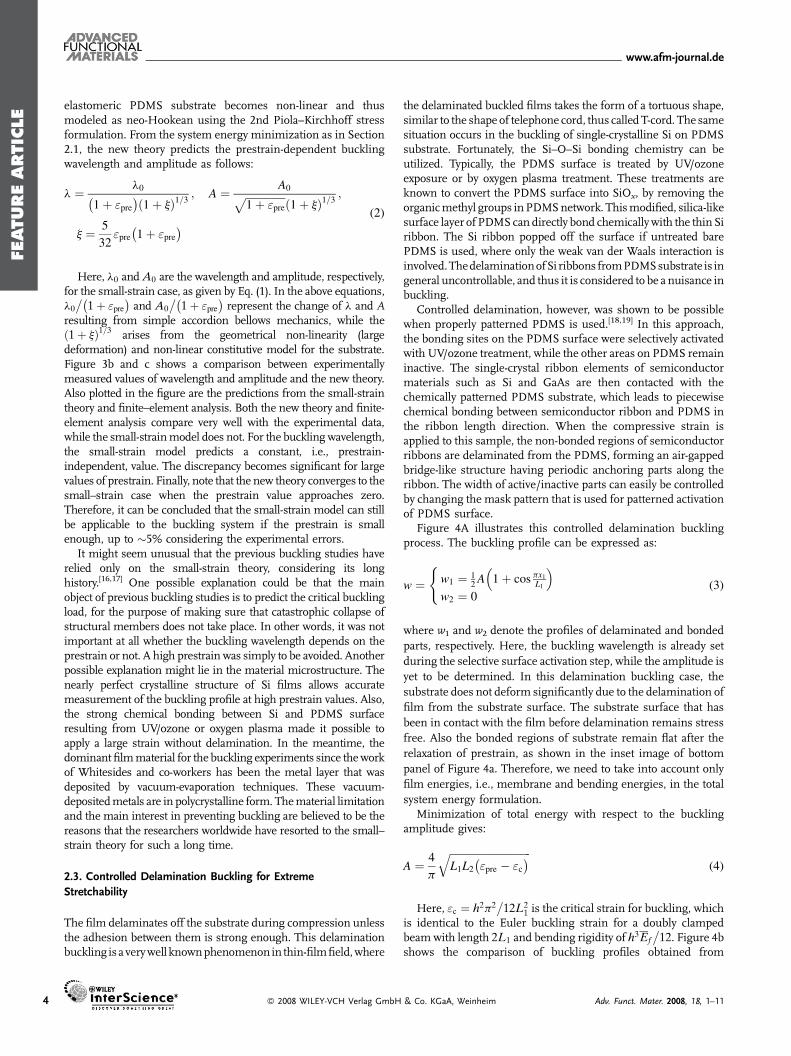
Figure 5. An schematic demonstration of width effect on buckling wavelength is shown in
(a). Note that the narrower the ribbon, the shorter the buckling wavelength. b) Stacked AFM
plane-view images of buckled Si (100 nm) ribbons with different widths of 2, 5, 20, 50, and
100mm (from top to bottom). A wavepeak in each image is aligned at the left and marked with a
long line, and their forth wavepeaks are marked with short lines, indicating the variation of
wavelength with respect to the ribbon width. The comparison between experiments and analytic
modeling for width effect are shown in (c) and (d). Reproduced with permission from Ref. [20].
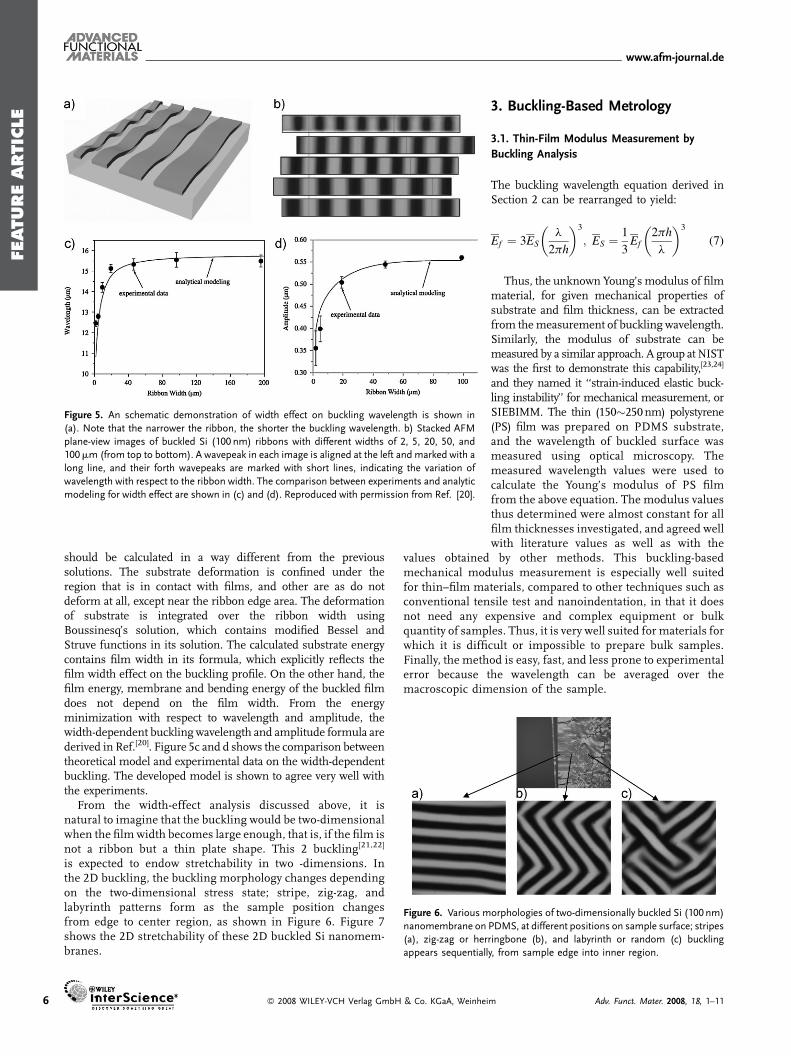
Figure 6. Various morphologies of two-dimensionally buckled Si (100 nm)
nanomembrane on PDMS, at different positions on sample surface; stripes
(a), zig-zag or herringbone (b), and labyrinth or random (c) buckling
appears sequentially, from sample edge into inner region.
6
should be calculated in a way different from the previoussolutions. The substrate deformation is confined under theregion that is in contact with films, and other are as do notdeform at all, except near the ribbon edge area. The deformationof substrate is integrated over the ribbon width usingBoussinesq’s solution, which contains modified Bessel andStruve functions in its solution. The calculated substrate energycontains film width in its formula, which explicitly reflects thefilm width effect on the buckling profile. On the other hand, thefilm energy, membrane and bending energy of the buckled filmdoes not depend on the film width. From the energyminimization with respect to wavelength and amplitude, thewidth-dependent buckling wavelength and amplitude formula arederived in Ref.[20]. Figure 5c and d shows the comparison betweentheoretical model and experimental data on the width-dependentbuckling. The developed model is shown to agree very well withthe experiments.
From the width-effect analysis discussed above, it isnatural to imagine that the buckling would be two-dimensionalwhen the film width becomes large enough, that is, if the film isnot a ribbon but a thin plate shape. This 2 buckling[21,22]
is expected to endow stretchability in two -dimensions. Inthe 2D buckling, the buckling morphology changes dependingon the two-dimensional stress state; stripe, zig-zag, andlabyrinth patterns form as the sample position changesfrom edge to center region, as shown in Figure 6. Figure 7shows the 2D stretchability of these 2D buckled Si nanomem-branes.
� 2008 WILEY-VCH Verlag GmbH & Co. KGaA, Weinhei
3. Buckling-Based Metrology
3.1. Thin-Film Modulus Measurement by
Buckling Analysis
The buckling wavelength equation derived inSection 2 can be rearranged to yield:
Ef ¼ 3ES
l
2ph
� �3
; ES ¼1
3Ef
2ph
l
� �3
(7)
Thus, the unknown Young’s modulus of filmmaterial, for given mechanical properties ofsubstrate and film thickness, can be extractedfrom themeasurement of buckling wavelength.Similarly, the modulus of substrate can bemeasured by a similar approach. A group at NISTwas the first to demonstrate this capability,[23,24]
and they named it ‘‘strain-induced elastic buck-ling instability’’ for mechanical measurement, orSIEBIMM. The thin (150�250nm) polystyrene(PS) film was prepared on PDMS substrate,and the wavelength of buckled surface wasmeasured using optical microscopy. Themeasured wavelength values were used tocalculate the Young’s modulus of PS filmfrom the above equation. The modulus valuesthus determined were almost constant for allfilm thicknesses investigated, and agreed wellwith literature values as well as with the
values obtained by other methods. This buckling-basedmechanical modulus measurement is especially well suitedfor thin–film materials, compared to other techniques such asconventional tensile test and nanoindentation, in that it doesnot need any expensive and complex equipment or bulkquantity of samples. Thus, it is very well suited for materials forwhich it is difficult or impossible to prepare bulk samples.Finally, the method is easy, fast, and less prone to experimentalerror because the wavelength can be averaged over themacroscopic dimension of the sample.
m Adv. Funct. Mater. 2008, 18, 1–11

FEATUREARTIC
LE
www.afm-journal.de
Figure 8. Modulus measurement of SWNTs by buckling. a) AFM image of
buckled SWNTs on PDMS. b) Comparison between experimentally
measured buckling wavelengths and calculation (gray lines). The modulus
of SWNT is calculated to be 1.3� 0.2 TPa. Reproduced with permission
from Ref. [28].
Figure 7. Optical micrographs of 2D wavy Si (100 nm) nanomembranes
on PDMS under stretching into three different directions. The white arrows
in the top frames denote the stretching direction, and the applied strain
values are given next to rightmost images for each frame. Reproduced with
permission from Ref. [21].
The mechanical modulus of polyelectrolyte multilayer (PEM)was also successfully determined using this method.[25,26]
Also, the modulus of soft substrate was determined in a similarway.[27] Further, it was demonstrated that the modulus of nano- ormolecular-scale materials such as SWNTs[28] and cross linkedSAM[29] can be determined by the buckling method. Figure 8Ashows the AFM image of the buckled, wavy SWNT arrays on
Figure 9. Mechanical modulus of P3HT and P3HT/PCBM films. Optical microscopy images for
buckled P3HT and P3HT/PCBM films in (a) and (c), respectively. The insets show the chemical
structure of P3HT and PCBM in the images. Measured wavelength data are plotted in (b) and (d),
as a function of film thickness, where the green lines are fitted results.
PDMS. The buckling wavelength of SWNTs,which depends on the nanotube diameter, wasmeasured by high-resolution AFM and plottedin Figure 8B. Fitting themeasured dependenceof wavelength on tube diameter has led toYoung’s modulus of SWNT of 1.3� 0.2 TPa,which is in quantitative agreement with thereported literature values.
3.2. Mechanical Modulus of Functional
Organics
Recently, there has been a lot of effort to useorganic materials such as conducting orsemiconducting polymers and oligomers, forflexible electronics. It is important to know themechanical properties of the materialsinvolved in flexible applications, which wouldbe needed to design fabrication processes suchas roll-to-roll schemes and to study themechanical behavior of final products duringservice. In general, however, it is not easy orrealistic to make these organic materials into abulk form for mechanical tests. In particular,these materials are used as a film in electronicsapplications and therefore, the buckling-basedmechanical characterization of these materialsshould be particularly useful.
Adv. Funct. Mater. 2008, 18, 1–11 � 2008 WILEY-VCH Verl
As an example, we determined the Young’s modulus of poly(3-hexylthiophene) (P3HT) and its blend with fullerene derivative,6,6-phenyl-C61-butyric acid methyl ester (PCBM).[30] P3HT hasbeen widely used as an active semiconductor material in organicfield effect transistor (OTFT),whileP3HT/PCBMcomposite showsgood photovoltaic conversion efficiency in a bulk heterojunction(BHJ) form. These organic electronic devices can be fabricated onplastic substrate such that the final product can be bendable. TheP3HTor P3HT/PCBM filmwas spun on glass substrate, on whichfluorinated SAM (F-SAM) was coated. The film on glass could beeasily picked-up onto PDMS, due to conformal contact of PDMSand low adhesionoffilmon theSAM-coated glass. The pickedfilm/PDMS was loaded on a home-made stage and buckled bycompression. Figure 9a (pure P3HT) and 9c (P3HT/PCBM blend)
ag GmbH & Co. KGaA, Weinheim 7

FEATUREARTIC
LE
www.afm-journal.de
Figure 10. a) AFM images (left) and section profiles (right) of wavy Si ribbons on PDMS. The
images correspond to compressed, unperturbed, and stretched state along the ribbon direction,
from top to bottom. b) The change of wavelength (curved line) and amplitude (straight line) of
wavy Si ribbons as a function of external strain (top). The maximum, or peak, strain as a function
of external strain is shown in the bottom panel. Reproduced with permission from Ref. [13].
8
shows the opticalmicroscopy images of buckledfilms. Thebucklingwavelengthwas determinedbymeasuring the distance betweenmanywaves(typically 10�20 waves) and dividing it by thenumber ofwaves containedwithin. This leads toamore accurate value than that fromsinglewavemeasurement, because of averaging of manywaves that have different wavelength values.Figure9banddshows theplotofwavelengthasafunction of film thickness, from which themechanical modulus is extracted. The P3HT/PCBM blend has much larger, �5 times,modulus (6.2GPa) than that of pure P3HT(1.3GPa). This highmodulus of composite filmmay be attributed to the filler effect of PCBMnanoparticles.
It is well known that the detailed nanoscalemorphology of P3HT/PCBM composite hassignificant effect on the solar cell perfor-mance.[31,32] The bi-continuous, nanoscalephase separated composite morphology yieldsa much higher solar cell efficiency than therandom mixture, because the photogenerated
carriers can be efficiently separated and collected when theymovealong continuous paths to the collecting electrodes. Therefore, itwould be interesting to check if there is any difference in themechanical property between phase-separated and randomcomposites. For this, one set of P3HT/PCBM composite film samples was annealed at 100 8C for 3 h toinduce the nanophase separation, while theother was not. The results (not shown here)showed that there is no noticeable difference inthe mechanical modulus of composite films,irrespective of thermal annealing and thusnanophase separation.Figure 11. Examples of stretchable electronic devices. The opticalmicroscopy images of buckled Si
ribbons on PDMS, having pn-junction diodes and thin film transistors on them, for compressed,
unperturbed, and stretched states, are shown in (a) and (c), respectively. The bottom part of (c)
shows the structure of a transistor device, which is a self-aligned, Schottky metal-oxide-semicon-
ductor field effect transistor (MOSFET). Reproduced with permission from Ref. [13].
4. Stretchable Electronics
4.1. Stretchable Metal Interconnection[33–36]
One of the direct applications of buckled thinfilm of metals on elastomeric substrate is thestretchable interconnection, that is, electricalconnection among devices and/or devices tothe outside world. Here, the devices may bestretchable itself, or they may be stiff. In thelatter case, the elastomeric substrate wouldhave rigid device islands interconnected bybuckled metal layers on it, and thus the wholesample would be stretchable because anexternally applied strain will mainly beabsorbed by the buckled metal parts.
In this approach, a thin metal layer isdeposited on a prestretched elastomeric sub-strate, in which the metal will be buckled intowavy, sinusoidal shape after the release ofprestrain. As expected, the buckled film showsalmost constant resistance up to�100% degree
� 2008 WILEY-VCH Verlag GmbH
of stretching, which is mainly determined by the prestrain appliedduring film deposition. Also this process is reversible withinexperimental error. On the other hand, the flat metal film showsalmost linear increase in resistance with stretching. As a realimplementations of this stretchable interconnection, the amor-
& Co. KGaA, Weinheim Adv. Funct. Mater. 2008, 18, 1–11

FEATUREARTIC
www.afm-journal.de
phous Si thin-film transistors (TFTs) made on polyimide foil werefaced down on contact pads forming inverter circuits, while theinterconnectionamong themwasmadeusingbuckledAufilm.Thebuckled, wavy metal interconnection worked well even underthe stretching, i.e., the whole circuit of rigid device islandsconnected by buckledmetal still worked well under the stretching.This simple approach is expected to open the first market forstretchable electronics products such as hairband-type thermo-meter, and toys.
LE
4.2. High-Performance Stretchable Electronics Using Buckled
Single-Crystal Inorganics
Although most inorganic, single-crystal semiconductor materialssuch as Si, GaAs, and InP are notorious for their brittleness,it was demonstrated that these materials are flexible enough to beused for bendable electronics, if they are made thin.[37–39]
Therefore, it is expected that the thin-film form of these materialscan also be made into wavy shape through buckling. The thinsingle-crystal Si layer was the first that was made into buckled,wavy shape, as already discussed in Section 2 in terms of bucklingmechanics. For the stretchable applications, however, it isimportant to understand not only the initial buckling mechanics,but also the post-buckling mechanics. Here, the post-bucklingmechanics has to do with the response of buckled material to anexternally applied strain. Intuitively, one can surmise that thesinusoidal surface will change to one with different periodicityand amplitude when stretched or compressed, as shown inFigure 10a. In stretchable electronic applications, the maximumstrain in the active semiconductor material is the most importantfactor to be considered, because the material will fracture or failabove a certain limit of strain. In an ideally sinusoidal buckledfilm, the maximum strain occurs at wave peaks or troughswhere the curvature is the highest. Assuming that the surfaceprofile is sinusoidal such that w ¼ A sin 2px=l
� �, the maximum
strain is given by:
"max ¼2p2Ah
l2(8)
Because the fracture limit of typical inorganic semiconductors
Figure 12. Schematic fabrication steps for two-dimensionally stretchable
electronic devices (bottom frame of left column), and cross-sectional view
with neutral mechanical plane indicated with a red dashed line (bottom
frame of right column). The optical images of circuits on the carrier wafer
(with single CMOS as an inset), on a thin rod, and in a wavy configuration
on PDMS, are shown in (b), (c), and (d), respectively. Reproduced with
permission from Ref. [40].
is around 2%, themaximum strain in the buckledmaterial shouldbe less than the fracture limit to prevent failure. In the example ofFigure 10, the values of wavelength and amplitude are �15 and1mm, respectively. Therefore, the maximum strain is�1%, whilethe applied strain is �5%. In other words, the activesemiconductor material experiences substantially less strainthan the externally applied strain, which makes stretchingpossible.
The fabrication of stretchable Si electronic devices is similar tothat of wavy Si, except that the Si ribbon elements have additionallayers such as dielectrics, and contact metals. All the high–temperature processing steps such as doping or thermaloxidation are usually done before the Si ribbons are transferredto elastomeric substrate, because the elastomeric substrate isincompatible with such high temperature steps. Then, the wetremoval of underlying oxide layer releases the Si ribbons havingdevice structure. Note that the devices are passivated to protect
Adv. Funct. Mater. 2008, 18, 1–11 � 2008 WILEY-VCH Verl
them from wet etching chemicals prior to the etching. Whenpicked up by PDMS substrate, however, the upside of the ribbonsis down, which makes subsequent device characterizationsimpossible because the contact metals are now buried below thesurface. To flip over the ribbons again, another piece of PDMSwas used. A stickier form of PDMS, or partially cured PDMS, wasused for this purpose.
As a simple example of stretchable Si electronics, two-terminalpn diodes and three-terminal field–effect transistors werefabricated and tested, as shown in Figure 11. In both cases,the initial wavy configuration could be reversibly converted to flator wavier shape, upon stretching or compressing, respectively(Fig. 11a and c). Also, the devices were functioning well duringand after the external straining. The scattering of data inFigure 11b and d is mainly due to irreproducible probe contactonto these devices; it is very difficult to make reliable andreproducible electrical contact on thin film devices that arefabricated on the very soft elastomeric substrate.
An alternative to 2D stretching is to use an ultrathin base layerwith arbitrarily-shaped semiconductor elements, as shown inFigure 12.[40] Although the semiconductor elements are too smallto have two-dimensional buckling characteristics as shown in
ag GmbH & Co. KGaA, Weinheim 9

FEATUREARTIC
LE
www.afm-journal.de
10
Figure 12, the ultrathin base layer that is supporting theseelements can buckle in two-dimensional space when it is placedon prestretched elastomeric substrate. Using this approach, twodimensionally stretchable electronic circuits such as comple-mentary metal/oxide/semiconductor (CMOS) and ring oscillatorcircuits are successfully demonstrated in Ref. [40].
5. Conclusions
In this article, we have demonstrated that the mechanicalbuckling phenomenon is no longer a problem to be avoided as in,for instance, structural mechanics. Rather, it is now finding novelapplications in various fields. Some of them are a simpleextension of or complement to existing technologies, while otherscan be whole new fields enabled by buckling.
Thin film form of materials is ubiquitous and nowindispensible in modern society. The mechanical property ofmaterials has long been determined on the basis of conventionaltesting protocols that need test specimens in bulk form. Incontrast, the metrology for materials in thin film form has neverbeen a simple task in itself. Furthermore, it is known that themechanical property of thin film of a material may differ fromthat of bulk due to larger surface to volume ratio. In some othercases, a material cannot be easily prepared in bulk shape. In thislight, the buckling-based determination ofmechanical property ofmaterials in thin film form is an invaluable addition, in that it issimple, fast, and easy to implement. It does not need any complexor expensive instruments. The results reported in this work, i.e.,modulus of functional organic materials, exemplify the kinds ofapplications that can be made with the technique. Betterunderstanding of mechanical characteristics of materials in thinfilm form would be very useful in emerging fields such as flexibleelectronics.
In the course of buckling study on single-crystal inorganicsemiconductors such as Si, we have found that the conventionalbuckling model has limited capability. It could not explain theexperimental results at large strain. The newly developed model,however, is shown to be applicable to large strain (up to �30%),while it reduces to the conventional model at small strain. Thewell-defined single-crystalline microstructure of material hasenabled to develop the general buckling model. In terms ofenhanced stretchability, the delamination buckling using spatiallycontrolled adhesion between film and substrate has been found tobe very useful. The mechanics model for the delaminationbuckling can be applicable to any materials, which may open avariety of applications using stretchable form of variousfunctional materials.
The application of buckled film on elastomeric substrate hasled to the realization of stretchable electronics, which is morechallenging than bendable ones. An example is the use ofmonocrystalline inorganic semiconductors, such as Si for theelectronic devices in stretchable form, which perform well evenunder the external loading such as stretching or compression.This may open the way to various unprecedented applications inwhich the devices can conform to the objects having unusualform factor including wearable electronics. For this to be realized,however, extensive studies would be required.
� 2008 WILEY-VCH Verlag GmbH
Acknowledgements
D.-Y. Khang acknowledges financial support from the Yonsei UniversityResearch Fund of 2008, and ‘‘System IC 2010’’ project of Korea Ministry ofCommerce, Industry and Economy. This article is part of a special issue onMaterials Science in Korea.
Recived: July 25, 2008
Revised: October 10, 2008
Published online:
[1] E. Cerda, L. Mahadevan, Phys. Rev. Lett. 2003, 90, 074302.
[2] J. Genzer, J. Groenewold, Soft Matter 2006, 2, 310.
[3] N. Bowden, S. Brittain, A. G. Evans, J. W. Hutchinson, G. M. Whitesides,
Nature 1998, 393, 146.
[4] P. J. Yoo, K. Y. Suh, S. Y. Park, H. H. Lee, Adv. Mater. 2002, 14, 1383.
[5] P. J. Yoo, H. H. Lee, Phys. Rev. Lett. 2003, 91, 154502.
[6] P. J. Yoo, S. Y. Park, S. J. Kwon, K. Y. Suh, H. H. Lee, Appl. Phys. Lett. 2003,
83, 4444.
[7] S. J. Kwon, P. J. Yoo, H. H. Lee, Appl. Phys. Lett. 2004, 84, 4487.
[8] P. J. Yoo, K. Y. Suh, H. Kang, H. H. Lee, Phys. Rev. Lett. 2004, 93, 034301.
[9] P. J. Yoo, H. H. Lee, Macromolecules 2005, 38, 2820.
[10] P. J. Yoo, H. H. Lee, Langmuir 2008, 24, 6897.
[11] J. Groenewold, Physica A 2001, 298, 32.
[12] Z. Y. Huang, W. Hong, Z. Suo, J. Mech. Phys. Solids 2005, 53, 2101.
[13] D.-Y. Khang, H. Jiang, Y. Huang, J. A. Rogers, Science 2006, 311, 208.
[14] H. Jiang, D.-Y. Khang, J. Song, Y. Sun, Y. Huang, J. A. Rogers, Proc. Natl.
Acad. Sci. USA 2007, 104, 15607.
[15] J. Song, H. Jiang, Z. J. Liu, D.-Y. Khang, Y. Huang, J. A. Rogers, C. Lu, C. G.
Koh, Int. J. Solids Struct. 2008, 45, 3107.
[16] S. P. Timoshenko, J. M. Gere, Theory of Elastic Stability, 2nd ed.,
McGraw-Hill, London 1961.
[17] H. G. Allen, Analysis and Design of Structural Sandwich Panels, Pergamon
Press, London 1969.
[18] Y. Sun, W. M. Choi, H. Jiang, Y. Huang, J. A. Rogers, Nat. Nanotechnol.
2006, 1, 201.
[19] H. Jiang, Y. Sun, J. A. Rogers, Y. Huang, Appl. Phys. Lett. 2007, 90, 133119.
[20] H. Jiang, D.-Y. Khang, H. Fei, H. Kim, Y. Huang, J. Xiao, J. A. Rogers, J.
Mech. Phys. Solids 2008, 56, 2585.
[21] W. M. Choi, J. Song, D.-Y. Khang, H. Jiang, Y. Huang, J. A. Rogers, Nano
Lett. 2007, 7, 1655.
[22] J. Song, H. Jiang, W. M. Choi, D.-Y. Khang, Y. Huang, J. A. Rogers, J. Appl.
Phys. 2008, 103, 014303.
[23] C. M. Stafford, C. Harrison, K. L. Beers, A. Karim, E. J. Amis, M. R.
Vanlandingham, H.-C. Kim, W. Volksen, R. D. Miller, E. E. Simonyi, Nat.
Mater. 2004, 3, 545.
[24] C. M. Stafford, B. D. Vogt, C. Harrison, D. Julthongpiput, R. Huang,
Macromolecules 2006, 39, 5095.
[25] A. J. Nolte, M. F. Rubner, R. E. Cohen, Macromolecules 2005, 38, 5367.
[26] A. J. Nolte, R. E. Cohen, M. F. Rubner, Macromolecules 2006, 39, 4841.
[27] E. A. Wilder, S. Guo, S. Lin-Gibson, M. J. Fasolka, C. M. Stafford,
Macromolecules 2006, 39, 4138.
[28] D.-Y. Khang, J. Xiao, C. Kocabas, S. MacLaren, T. Banks, H. Jiang, Y. Huang,
J. A. Rogers, Nano Lett. 2008, 8, 124.
[29] M. J. Schultz, X. Zhang, S. Unarunotai, D.-Y. Khang, Q. Cao, C. Wang, C.
Lei, S. Maclaren, J. A. N. T. Soares, I. Petrov, J. S. Moore, J. A. Rogers, Proc.
Natl. Acad. Sci. USA 2008, 105, 7353.
[30] D. Tahk, D.-Y. Khang, H. H. Lee, unpublished results.
[31] H. Hoppe, N. S. Sariftci, J. Mater. Chem. 2006, 16, 45.
[32] M. Campoy-Quiles, T. Ferenczi, T. Agnostinelli, P. G. Etchegoin, Y. Kim,
T. D. Anthopoulos, P. N. Stavrinou, D. D. Bradley, J. Nelson, Nat. Mater.
2008, 7, 158.
[33] S. P. Lacour, S. Wagner, Z. Huang, Z. Suo, Appl. Phys. Lett. 2003, 82, 2404.
& Co. KGaA, Weinheim Adv. Funct. Mater. 2008, 18, 1–11

FEATURE
www.afm-journal.de
[34] S. Wagner, S. P. Lacour, J. Jones, P. I. Hsu, J. C. Sturm, T. Li, Z. Suo, Physica E
2004, 25, 326.
[35] J. Jones, S. P. Lacour, S. Wagner, Z. Suo, J. Vac. Sci. Technol, A 2004, 22, 1723.
[36] S. P. Lacour, J. Jones, S. Wagner, T. Li, Z. Suo, Proc. IEEE 2005, 93, 1459.
[37] E. Menard, K. J. Lee, D.-Y. Khang, R. G. Nuzzo, J. A. Rogers, Appl. Phys. Lett.
2004, 84, 5398.
Adv. Funct. Mater. 2008, 18, 1–11 � 2008 WILEY-VCH Verl
[38] E. Menard, R. G. Nuzzo, J. A. Rogers, Appl. Phys. Lett. 2005, 86,
093507.
[39] Y. Sun, D.-Y. Khang, F. Hua, K. Hurley, R. G. Nuzzo, J. A. Rogers, Adv. Funct.
Mater. 2005, 15, 30.
[40] D.-H. Kim, J.-H. Ahn, W. M. Choi, H.-S. Kim, T.-H. Kim, J. Song, Y. Huang,
Z. Liu, C. Lu, J. A. Rogers, Science 2008, 320, 507.
A RTICLE
ag GmbH & Co. KGaA, Weinheim 11