mechanical magic of nanocrystalline substances · mechanical magic of nanocrystalline substances...
TRANSCRIPT
MECHANICAL MAGIC OF NANOCRYSTALLINE SUBSTANCES
M.DHARIK SANCHAN (CH04B017) VIJAY SHANKAR V (EP04B011) JIKKU M THOMAS (CH04B059) ANAND NATARAJAN (CH04B056) ANUSH KRISHNAN (AE04B002)
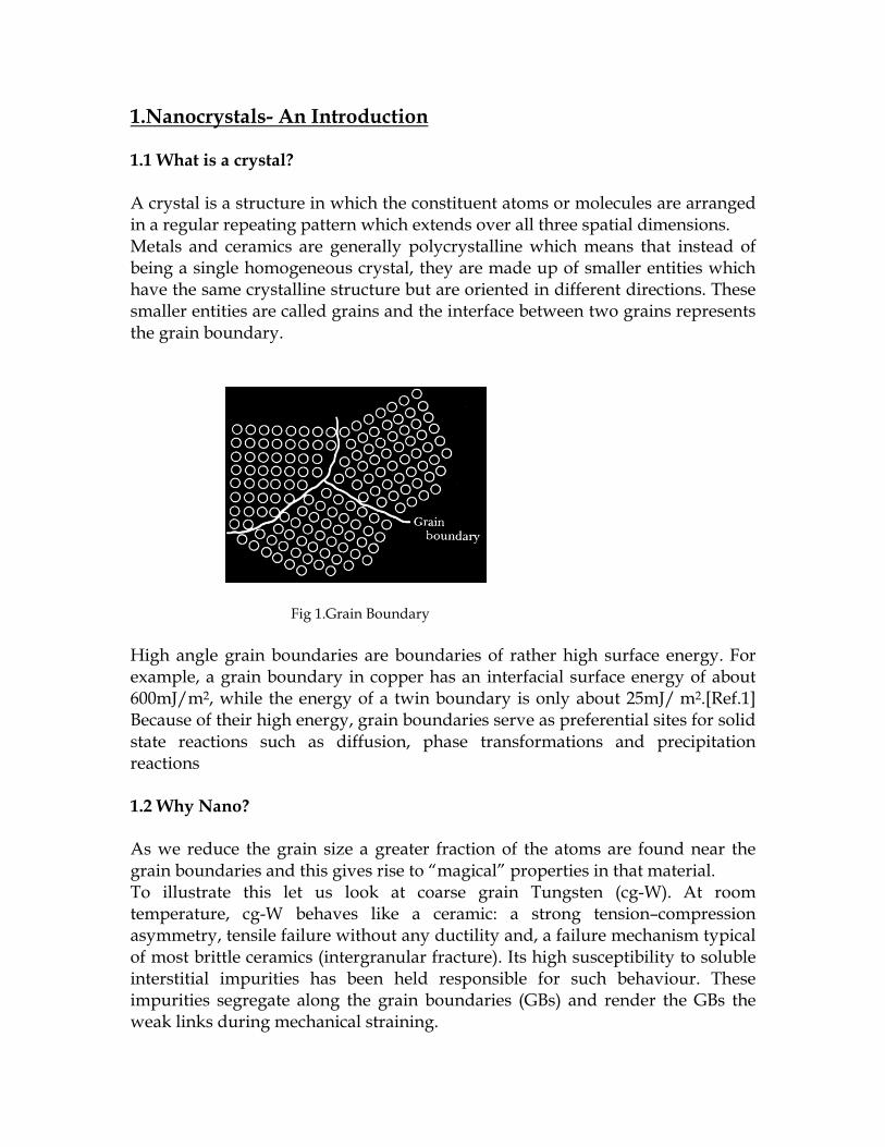
1.Nanocrystals- An Introduction 1.1 What is a crystal? A crystal is a structure in which the constituent atoms or molecules are arranged in a regular repeating pattern which extends over all three spatial dimensions. Metals and ceramics are generally polycrystalline which means that instead of being a single homogeneous crystal, they are made up of smaller entities which have the same crystalline structure but are oriented in different directions. These smaller entities are called grains and the interface between two grains represents the grain boundary.
Fig 1.Grain Boundary High angle grain boundaries are boundaries of rather high surface energy. For example, a grain boundary in copper has an interfacial surface energy of about 600mJ/m2, while the energy of a twin boundary is only about 25mJ/ m2.[Ref.1] Because of their high energy, grain boundaries serve as preferential sites for solid state reactions such as diffusion, phase transformations and precipitation reactions 1.2 Why Nano? As we reduce the grain size a greater fraction of the atoms are found near the grain boundaries and this gives rise to “magical” properties in that material. To illustrate this let us look at coarse grain Tungsten (cg-W). At room temperature, cg-W behaves like a ceramic: a strong tension–compression asymmetry, tensile failure without any ductility and, a failure mechanism typical of most brittle ceramics (intergranular fracture). Its high susceptibility to soluble interstitial impurities has been held responsible for such behaviour. These impurities segregate along the grain boundaries (GBs) and render the GBs the weak links during mechanical straining.

On the other hand, nanocrystalline Tungsten (nc-W) produced by high-pressure torsion (HPT) at low temperature (500°C) exhibits remarkably high strength (hardness ~11 GPa close to the disk edge, strength ~3.0 GPa under quasi-static and ~4.0 GPa under dynamic compression). Nanocrystalline Tungsten has mechanical strength comparable to that of some strong ceramics, and its quasi-static and dynamic failure is not completely brittle (compared to cg-W) [2]. The changes in the mechanical properties due to reduction in grain sizes are attributed to the fact that a larger percentage of the atoms are expected to be in grain boundary environments with broken bonds and amorphous regions. [1] A rough estimate shows that the volume fraction at the grain boundaries is given by 3δ/D, where δ is the width of the boundary and D is the grain size. Thus, the fraction of atoms at the boundaries increases from 25% for 12 nm to 100% for 3 nm grain size, assuming that δ is 1.0 nm. In addition, the mechanical properties will be affected by other features such as flaws, strains, impurities, etc., that result from synthesis and processing [1] 2. STRENGTH OF A NANOCRYSTAL: 2.1 Hall-Petch Relation: A general relationship between yield stress and grain size is given by the following correlation [1]:
0k
i dσ σ= + (1)
0σ - Yield stress iσ - ”Friction stress”, representing the overall resistance of the crystal lattice to
dislocation movement.
k - “Locking parameter” d- Grain diameter However, this relation is valid only up to a certain grain size, below which a softening effect is observed. This region, below the critical grain size, exhibits a negative Hall-Petch effect.
Fig2.Graph showing variation of hardness with grain size. [3]

The above figure shows the variation of hardness (a mechanical property which measures a material’s resistance to permanent deformation.) with reducing grain size. A plateau, followed by a decrease in hardness for grain size in the region of 25nm is observed. This negative trend has been attributed to diffusional creep in nanocrystalline samples at room temperature analogous to grain-boundary sliding in conventionally-grained samples at high temperature. The above hardness (H) has been measured in terms of the flow stress(σ) of substances. (H≈3σ)Flow stress is defined as the specific value of shear stress required to cause plastic deformation [3].
Fig3. Hardness Vs log d describing behaviour below the critical grain size (dc). [3]
As we can see the critical grain size lies in the nano range and this is one of the reasons why the nano regime is of great importance for developing materials with extreme mechanical properties. Nanocrystals are those materials with grain size (d) in the range 10-100nm. 3. MECHANICAL PROPERTIES OF NANOCRYSTALS: 3.1 Hardness Hardness as described above is the resistance of a material to permanent deformation. It can be measured by uniaxial tensile or compression tests and nano or micro indentation techniques such as the Vicker’s Hardness Test.
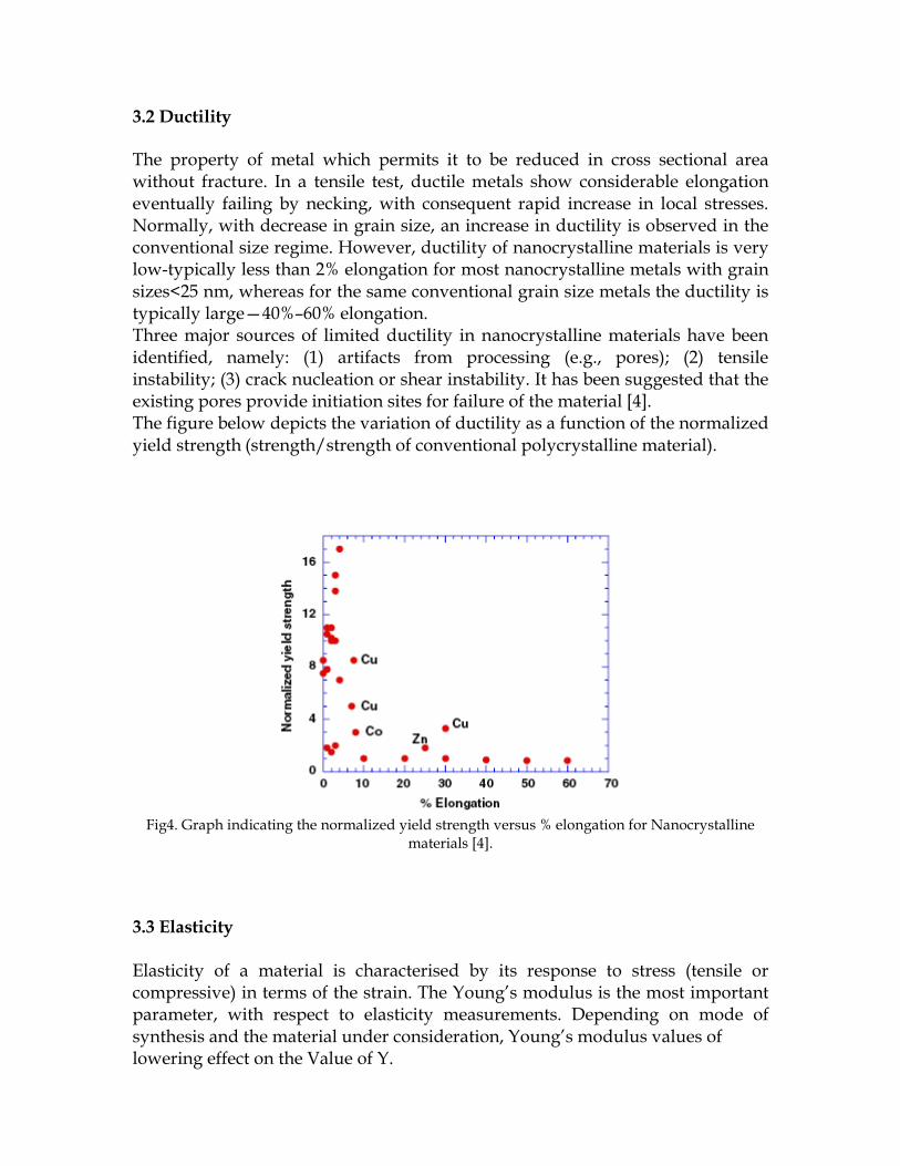
3.2 Ductility The property of metal which permits it to be reduced in cross sectional area without fracture. In a tensile test, ductile metals show considerable elongation eventually failing by necking, with consequent rapid increase in local stresses. Normally, with decrease in grain size, an increase in ductility is observed in the conventional size regime. However, ductility of nanocrystalline materials is very low-typically less than 2% elongation for most nanocrystalline metals with grain sizes<25 nm, whereas for the same conventional grain size metals the ductility is typically large—40%–60% elongation. Three major sources of limited ductility in nanocrystalline materials have been identified, namely: (1) artifacts from processing (e.g., pores); (2) tensile instability; (3) crack nucleation or shear instability. It has been suggested that the existing pores provide initiation sites for failure of the material [4]. The figure below depicts the variation of ductility as a function of the normalized yield strength (strength/strength of conventional polycrystalline material).
Fig4. Graph indicating the normalized yield strength versus % elongation for Nanocrystalline
materials [4].
3.3 Elasticity Elasticity of a material is characterised by its response to stress (tensile or compressive) in terms of the strain. The Young’s modulus is the most important parameter, with respect to elasticity measurements. Depending on mode of synthesis and the material under consideration, Young’s modulus values of lowering effect on the Value of Y.
Nucleation density also has major impact on the Young’s Modulus. For example, Y values can vary from 500 GPa to 1200 GPa for nanocrystalline diamond films, depending on the nucleation density. 4. SYNTHESIS Synthesis determines the properties of nanocrystalline materials to a very large extent. Because of their high surface area, nanocrystalline materials are prone to reaction at the surface and consolidation. Proper techniques for achieving desired grain size, avoiding contamination and reaction, strong bonding of the grains are of utmost importance in the production of nanocrystalline materials with desirable properties. Hence, synthesis is of crucial importance in deciding properties of the product. The two major approaches employed to nanocrystalline material are the bottom up approach, where the nanostructure is assembled atom by atom, layer by layer; and the top down approach which involves breaking down the polycrystalline bulk material to crystalline units with nano dimensions. The following are a few of the important techniques for the synthesis of these materials [4]: 1. Inert Gas Condensation 2. Mechanical Alloying 3. Electrodeposition 4. Crystallisation from amorphous solids 5. Severe Plastic Deformation 6. Chemical Vapour Deposition
5. PARAMETERS AFFECTING THE MECHANICAL PROPERTIES: In general, a nanocrystalline film’s mechanical properties depend on a number of parameters, the significant ones being mentioned below:
• Nucleation density at the time of synthesis
• Grain size
• Porosity of the crystal formed
• Presence of an additional phase in the crystal To illustrate the importance of these parameters, we will be looking at a different nanocrystalline films, and synthesised by different process routes.
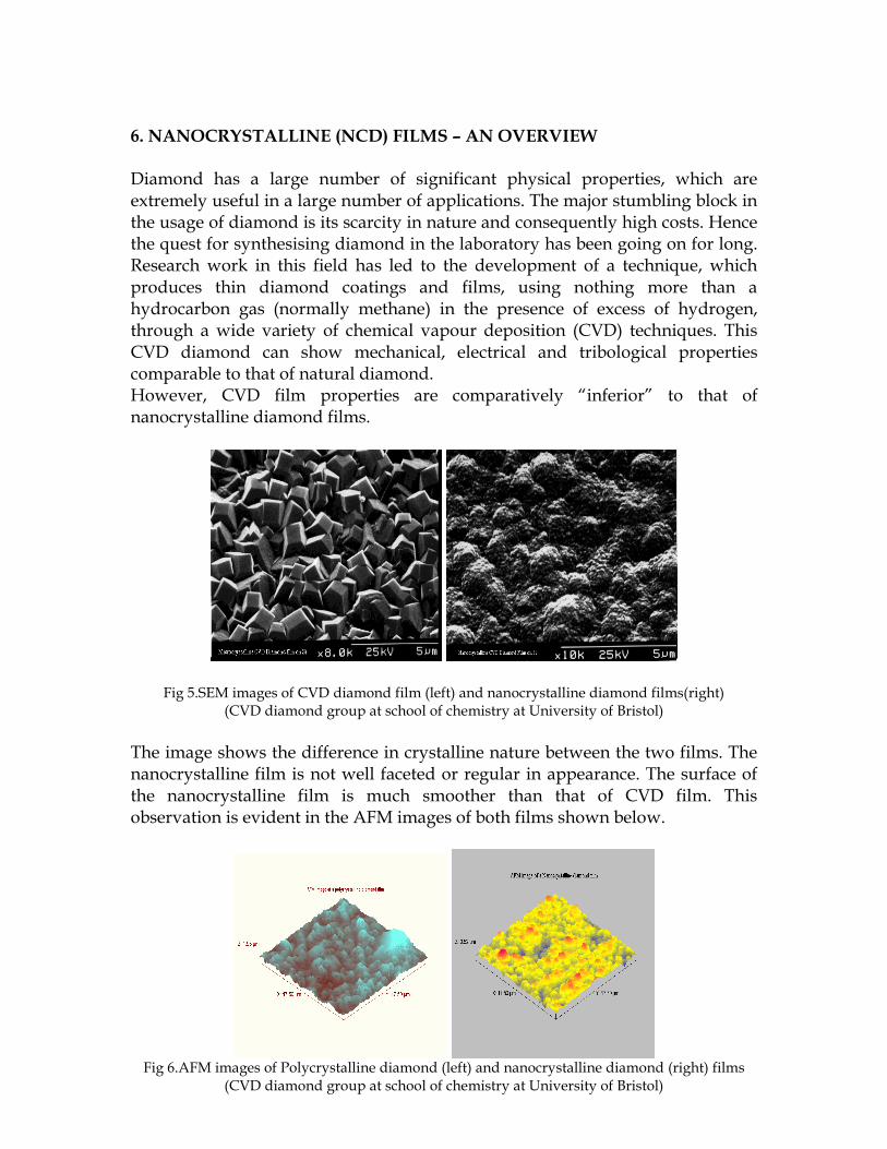
6. NANOCRYSTALLINE (NCD) FILMS – AN OVERVIEW Diamond has a large number of significant physical properties, which are extremely useful in a large number of applications. The major stumbling block in the usage of diamond is its scarcity in nature and consequently high costs. Hence the quest for synthesising diamond in the laboratory has been going on for long. Research work in this field has led to the development of a technique, which produces thin diamond coatings and films, using nothing more than a hydrocarbon gas (normally methane) in the presence of excess of hydrogen, through a wide variety of chemical vapour deposition (CVD) techniques. This CVD diamond can show mechanical, electrical and tribological properties comparable to that of natural diamond. However, CVD film properties are comparatively “inferior” to that of nanocrystalline diamond films.
Fig 5.SEM images of CVD diamond film (left) and nanocrystalline diamond films(right) (CVD diamond group at school of chemistry at University of Bristol)
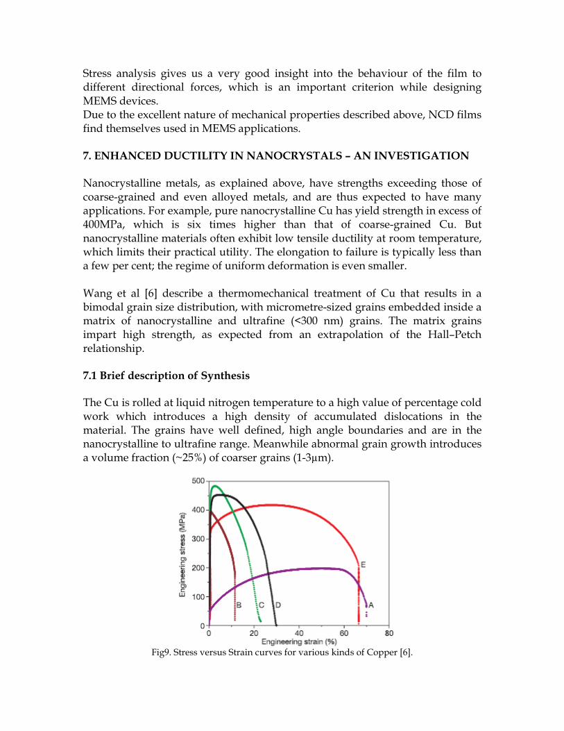
The image shows the difference in crystalline nature between the two films. The nanocrystalline film is not well faceted or regular in appearance. The surface of the nanocrystalline film is much smoother than that of CVD film. This observation is evident in the AFM images of both films shown below.
Fig 6.AFM images of Polycrystalline diamond (left) and nanocrystalline diamond (right) films
(CVD diamond group at school of chemistry at University of Bristol)

6.1 Applications in MEMS Diamond films have been found to be useful in microelectromechanical systems (MEMS).Usually polycrystalline diamond films have excellent mechanical properties which make them frontrunners for usage in MEMS applications. However, owing to the surface roughness exhibited by these polycrystalline films and due to the inhomogeneous grain size distribution that is observed in a layer, they show uncontrollable embedded stress. Nanocrystalline diamond (NCD) films can overcome most of the drawbacks of polycrystalline films by achieving a very low surface roughness. The homogeneous grain structure of indicates a more uniform distribution of stress in a layer [5]. They satisfy the important prerequisite of having excellent mechanical properties, so as to be used in MEMS. 6.2 HFCVD method and the mechanical properties of NCD Films 6.2.1 Process description (in brief):
• Firstly, generating homogeneous and relatively high nucleation density (>1010cm2) on the substrate (Si wafer 4in.diameter) through a bias enhanced nucleation.
• Then, the NCD film is grown at a filament temperature of 2200°C, a methane concentration of 0.3%, and with varying substrate temperature, nitrogen concentration and pressure. To avoid the growth of polycrystalline films during the process, renucleation is necessary. This results in a fine NCD film being formed.
6.2.2 Mechanical properties:
Fig7. Graph showing variation of fracture strength and Young’s modulus with film thickness [5].

• As can be seen from the graph, the value of fracture strength and Young’s modulus for NCD films are nearly independent of the film thickness.
• The experimental range of fracture strength was found to be between 3.2-3.9 GPa.
• The higher than expected values of Y are explained by the higher nucleation density [6].
Stress Analysis: To perform stress analysis in a thin layer of the film, the stress tensor was simplified in to two components:
• The gradient stress (acting vertically)
• The built -in stress (acting laterally)
These two stresses were analysed through different test mechanisms. The gradient stress was measured by means of constructing single side anchored cantilevers, while the built- in stress was measured by constructing double side anchored freestanding cantilevers. The gradient stress represents the differential stress across the layer thickness and it is equivalent to a force perpendicular to the plane of the layer. This stress is mainly related to the inhomogeneity of the grain size in the vertical dimension of the layer. Due to the highly homogeneous vertical grain distribution in the NCD films, these films are almost gradient stress free (<40MPa). The built-in stress (compressive and tensile) was measured as a function of parameters of the synthesis process and the following graphical observation was seen.
Fig8. Graph showing the compressive stress dependence on substrate temperature and pressure at constant N/C ratio of 70% [5].
Stress analysis gives us a very good insight into the behaviour of the film to different directional forces, which is an important criterion while designing MEMS devices. Due to the excellent nature of mechanical properties described above, NCD films find themselves used in MEMS applications. 7. ENHANCED DUCTILITY IN NANOCRYSTALS – AN INVESTIGATION Nanocrystalline metals, as explained above, have strengths exceeding those of coarse-grained and even alloyed metals, and are thus expected to have many applications. For example, pure nanocrystalline Cu has yield strength in excess of 400MPa, which is six times higher than that of coarse-grained Cu. But nanocrystalline materials often exhibit low tensile ductility at room temperature, which limits their practical utility. The elongation to failure is typically less than a few per cent; the regime of uniform deformation is even smaller. Wang et al [6] describe a thermomechanical treatment of Cu that results in a bimodal grain size distribution, with micrometre-sized grains embedded inside a matrix of nanocrystalline and ultrafine (<300 nm) grains. The matrix grains impart high strength, as expected from an extrapolation of the Hall–Petch relationship. 7.1 Brief description of Synthesis The Cu is rolled at liquid nitrogen temperature to a high value of percentage cold work which introduces a high density of accumulated dislocations in the material. The grains have well defined, high angle boundaries and are in the nanocrystalline to ultrafine range. Meanwhile abnormal grain growth introduces a volume fraction (~25%) of coarser grains (1-3µm).
Fig9. Stress versus Strain curves for various kinds of Copper [6].
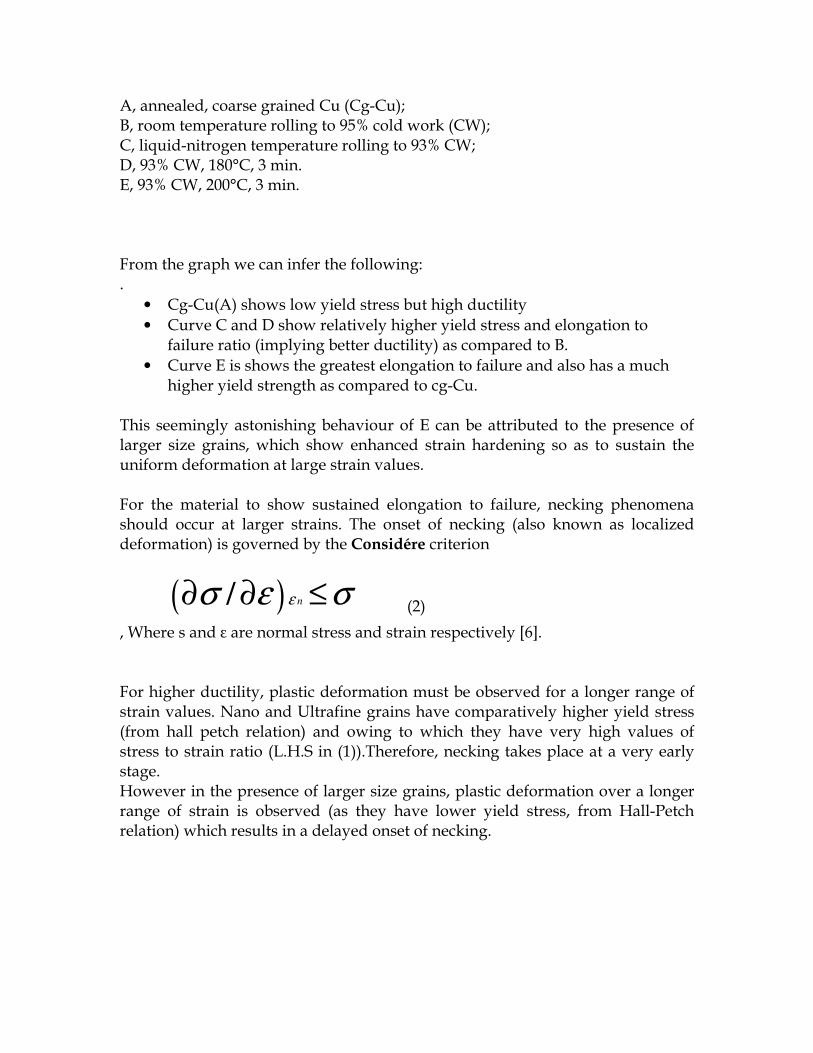
A, annealed, coarse grained Cu (Cg-Cu); B, room temperature rolling to 95% cold work (CW); C, liquid-nitrogen temperature rolling to 93% CW; D, 93% CW, 180°C, 3 min. E, 93% CW, 200°C, 3 min. From the graph we can infer the following: .
• Cg-Cu(A) shows low yield stress but high ductility
• Curve C and D show relatively higher yield stress and elongation to failure ratio (implying better ductility) as compared to B.
• Curve E is shows the greatest elongation to failure and also has a much higher yield strength as compared to cg-Cu.
This seemingly astonishing behaviour of E can be attributed to the presence of larger size grains, which show enhanced strain hardening so as to sustain the uniform deformation at large strain values. For the material to show sustained elongation to failure, necking phenomena should occur at larger strains. The onset of necking (also known as localized deformation) is governed by the Considére criterion
( )/ nεσ ε σ∂ ∂ ≤ (2)
, Where s and ε are normal stress and strain respectively [6]. For higher ductility, plastic deformation must be observed for a longer range of strain values. Nano and Ultrafine grains have comparatively higher yield stress (from hall petch relation) and owing to which they have very high values of stress to strain ratio (L.H.S in (1)).Therefore, necking takes place at a very early stage. However in the presence of larger size grains, plastic deformation over a longer range of strain is observed (as they have lower yield stress, from Hall-Petch relation) which results in a delayed onset of necking.
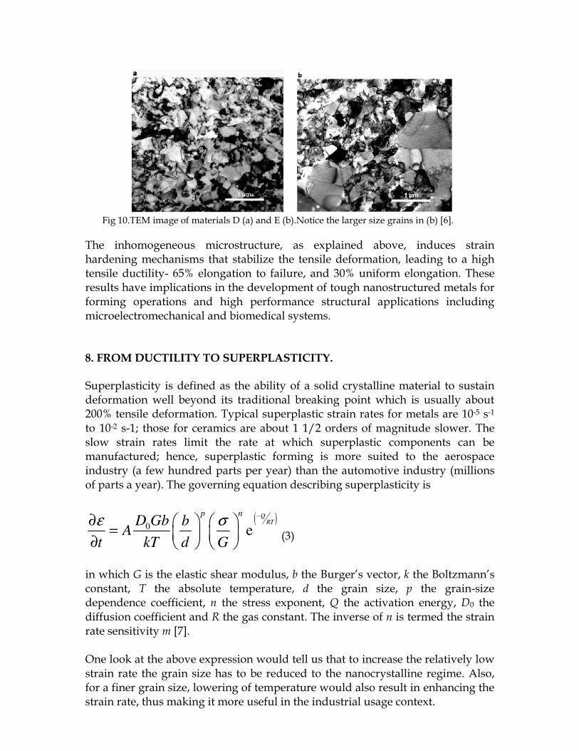
Fig 10.TEM image of materials D (a) and E (b).Notice the larger size grains in (b) [6].
The inhomogeneous microstructure, as explained above, induces strain hardening mechanisms that stabilize the tensile deformation, leading to a high tensile ductility- 65% elongation to failure, and 30% uniform elongation. These results have implications in the development of tough nanostructured metals for forming operations and high performance structural applications including microelectromechanical and biomedical systems. 8. FROM DUCTILITY TO SUPERPLASTICITY.
Superplasticity is defined as the ability of a solid crystalline material to sustain deformation well beyond its traditional breaking point which is usually about 200% tensile deformation. Typical superplastic strain rates for metals are 10-5 s-1 to 10-2 s-1; those for ceramics are about 1 1/2 orders of magnitude slower. The slow strain rates limit the rate at which superplastic components can be manufactured; hence, superplastic forming is more suited to the aerospace industry (a few hundred parts per year) than the automotive industry (millions of parts a year). The governing equation describing superplasticity is
( )0 e
QRT
p nD Gb b
At kT d G
ε σ −∂
= ∂
(3)
in which G is the elastic shear modulus, b the Burger’s vector, k the Boltzmann’s constant, T the absolute temperature, d the grain size, p the grain-size dependence coefficient, n the stress exponent, Q the activation energy, D0 the diffusion coefficient and R the gas constant. The inverse of n is termed the strain rate sensitivity m [7]. One look at the above expression would tell us that to increase the relatively low strain rate the grain size has to be reduced to the nanocrystalline regime. Also, for a finer grain size, lowering of temperature would also result in enhancing the strain rate, thus making it more useful in the industrial usage context.
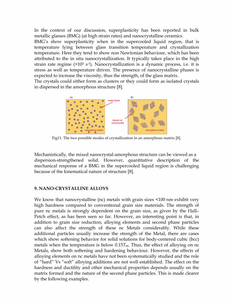
In the context of our discussion, superplasticity has been reported in bulk metallic glasses (BMG) (at high strain rates) and nanocrystalline ceramics. BMG’s show superplasticity when in the supercooled liquid region, that is temperature lying between glass transition temperature and crystallization temperature. Here they tend to show non Newtonian behaviour, which has been attributed to the in situ nanocrystallization. It typically takes place in the high strain rate regime (>103 s-1). Nanocrystallization is a dynamic process, i.e. it is stress as well as temperature driven. The presence of nanocrystalline phases is expected to increase the viscosity, thus the strength, of the glass matrix. The crystals could either form as clusters or they could form as isolated crystals in dispersed in the amorphous structure [8].
Fig11. The two possible modes of crystallization in an amorphous matrix [8].
Mechanistically, the mixed nanocrystal-amorphous structure can be viewed as a dispersion-strengthened solid. However, quantitative description of the mechanical response of a BMG in the supercooled liquid region is challenging because of the kinematical nature of structure [8]. 9. NANO-CRYSTALLINE ALLOYS We know that nanocrystalline (nc) metals with grain sizes <100 nm exhibit very high hardness compared to conventional grain size materials. The strength of pure nc metals is strongly dependent on the grain size, as given by the Hall–Petch effect, as has been seen so far. However, an interesting point is that, in addition to grain size reduction, alloying elements and second phase particles can also affect the strength of these nc Metals considerably. While these additional particles usually increase the strength of the Metal, there are cases which show softening behavior for solid solutions for body-centered cubic (bcc) metals when the temperature is below 0.15Tm. Thus, the effect of alloying on nc Metals, show both softening and hardening behaviour. However, the effects of alloying elements on nc metals have not been systematically studied and the role of “hard” Vs “soft” alloying additions are not well established. The effect on the hardness and ductility and other mechanical properties depends usually on the matrix formed and the nature of the second phase particles. This is made clearer by the following examples.
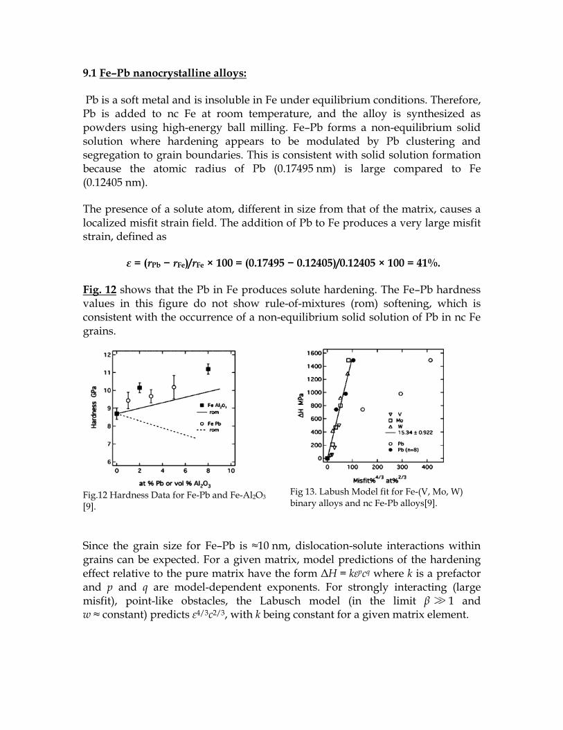
9.1 Fe–Pb nanocrystalline alloys: Pb is a soft metal and is insoluble in Fe under equilibrium conditions. Therefore, Pb is added to nc Fe at room temperature, and the alloy is synthesized as powders using high-energy ball milling. Fe–Pb forms a non-equilibrium solid solution where hardening appears to be modulated by Pb clustering and segregation to grain boundaries. This is consistent with solid solution formation because the atomic radius of Pb (0.17495 nm) is large compared to Fe (0.12405 nm).
The presence of a solute atom, different in size from that of the matrix, causes a localized misfit strain field. The addition of Pb to Fe produces a very large misfit strain, defined as
ε = (rPb − rFe)/rFe × 100 = (0.17495 − 0.12405)/0.12405 × 100 = 41%.
Fig. 12 shows that the Pb in Fe produces solute hardening. The Fe–Pb hardness values in this figure do not show rule-of-mixtures (rom) softening, which is consistent with the occurrence of a non-equilibrium solid solution of Pb in nc Fe grains.
Fig.12 Hardness Data for Fe-Pb and Fe-Al2O3 [9].
Fig 13. Labush Model fit for Fe-(V, Mo, W) binary alloys and nc Fe-Pb alloys[9].
Since the grain size for Fe–Pb is ≈10 nm, dislocation-solute interactions within grains can be expected. For a given matrix, model predictions of the hardening effect relative to the pure matrix have the form ∆H = kεpcq where k is a prefactor and p and q are model-dependent exponents. For strongly interacting (large misfit), point-like obstacles, the Labusch model (in the limit β 1 and w ≈ constant) predicts ε4/3c2/3, with k being constant for a given matrix element.

A plot of ∆H vs. ε4/3c2/3 for the Labusch model is shown in Fig. 13 (ε as % misfit and c as % solute). The correlation line shown is fit to the V, Mo and W results. Clearly, Pb does not produce solute hardening in proportion to its larger misfit (41%) when compared to the equilibrium solid solutions. There are two possible explanations for this effect. First, there can be solute segregation to the grain boundaries in Fe–Pb that removes solute from the grain interiors. An estimate for cube-shape grains shows that a monolayer of Pb on grain boundaries in Fe at a grain size of 10 nm would remove ≈7% Pb from solution (assuming that the volume/atom in a grain boundary is the same as the Fe lattice). There would be no solute hardening effect for our alloys in this fully saturated limit. Second, there can be clustering of the Pb atoms within grains. Clusters of size n would produce an effective atom fraction of c/n. A value of n = 8 for the Labusch model will “cluster-shift” the Pb data points onto the correlation line as shown in the figure i.e., the Fe–Pb hardening results would be consistent with the equilibrium solution results if eight-atom sized Pb clusters in Fe are formed.
We conclude from this analysis that misfit solute strengthening is present in Fe–Pb alloys, but its effect relative to equilibrium solutes could be modulated by Pb clustering accompanied by some degree (less than a monolayer) of Pb segregation to grain boundaries. This indicates that solute hardening for Pb in Fe is less effective than for equilibrium solid solution Fe-based alloys. [9]
Fe–Al2O3 Nanocomposites: Al2O3 is a hard insoluble ceramic that will be dispersed in the Fe matrix and the Fe–Al2O3 nanocomposites were prepared using ball milling. Fe–Al2O3 forms a nanocomposite and rule-of-mixtures hardening occurs with an additional contribution due to grain size reduction during milling.
Nanocomposite (rule of mixtures) type hardening can be anticipated for Fe–Al2O3 (≈50 nm Al2O3 particle size and ≈7 nm Fe grain size). Nanocomposite hardening occurs when the second-phase particles are larger than the matrix grain size because dislocation-particle interaction mechanisms will not be operative within single grains. However, the Fe–Al2O3 hardness values seen in Fig. 3 are noticeably higher than the rom line. A grain size decrease can result from additional (geometrically necessary) dislocation density introduced by the Al2O3 particles during milling. Al2O3 particles can also pin grain boundaries, stabilizing a finer nc grain structure. This reduced Fe-matrix grain size in the nanocomposites could account for the hardness increase, relative to the rule-of-mixtures prediction, observed in Fig. 14 for the 2 and 5 vol. % Al2O3 points.

Fig 14. Hardness of Fe-Pb and Fe-Al2O3 [9]
Fig 15. Hall-Petch Plot for Fe[9]
Fig. 15 shows a Hall–Petch (HP) plot extended to nc regime (d < 100 nm) using data, along with the HP line (dashed) for conventional Fe. The data points obtained here for pure nc Fe and the two predicted Fe-matrix values for f > 0 agree well with the other nc HP hardness values shown. While there is some scatter in the data in this figure, the values match quite closely with the correlation line (nc HP) fitted to the nc regime data points. The HP slope in the nc regime is clearly reduced, as has been observed for other metals. We conclude from this good agreement that the additional hardening for the Fe–Al2O3 nanocomposites seen in Fig. 14, relative to the rule-of-mixtures prediction, is consistent with Fe-matrix grain-size reduction during processing. Thus, we see that Fe–Al2O3 alloys contain Al2O3 dispersed particles with an average size almost an order of magnitude larger than the nc Fe-matrix grain size. Due to this size scale difference, a nanocomposite hardening effect results and is observed to follow the rule of mixtures. [9] Nc Al- nc PB Alloy: Al–Pb is a binary alloy system that exhibits a positive heat of mixing and a large miscibility gap between liquid and solid states and hence is the ideal system to obtain two phase structures. The presence of nanosized Pb particles in an Al matrix can result in depression or elevation of the melting point of Pb from its bulk value, depending on a coherent or incoherent interface between Pb/Al. Nanosized dispersions in a coarse grained matrix will produce dispersion hardening, and the effect of size and spacing between the particles on the mechanical properties on nc alloys are well known. The Al-Pb alloys can be formed by two methods. In the first, Al and Pb powders are loaded into a tool steel vial in a glove box under a high purity argon atmosphere and milled in a high energy Shaker mill, with the addition of 1.5 wt.% stearic acid as a surfactant in order to avoid cold welding.

The resultant powders are consolidated into 6.35 mm diameter disks. In the second processing route, spherical balls (of 8 mm maximum diameter) are consolidated in situ using a combination of milling at liquid nitrogen temperature and milling at room temperature. Consequently these spheres were transformed into disks.
Fig 15a. Variation of microhardness in in situ consolidated and hot compacted nanocrystalline Al–Pb alloys.[10]
Previously, it was thought that hardness of Al–Pb increased with increase in Pb content and the conclusion was that dispersion hardening was the strengthening mechanism. Figure 15a shows the hardness data obtained on hot compacted samples as well as in situ consolidated samples in the current study. Ball milled and hot compacted pure Al has a hardness of 925 MPa whereas in situ consolidated Al has a hardness of 900 MPa. An addition of 1.0% (atomic) of Pb results in drastic softening of nc Al matrix decreasing the strength by 35–37%! The effect of stearic acid on the measured hardness values of hot compacted samples is minimal as the same hardness levels are observed in the hot compacted samples (synthesized with stearic acid) and in the in situ consolidated samples (synthesized without stearic acid). These results are at variance with the previous conclusion, and therefore the only apparent reason for this softening is the nc Pb, its distribution and its interaction with nc Al grain boundaries.
From the obtained hardness data, it is clear that Pb is softening the nc Al matrix well below the values predicted by the rule of mixtures. The grain boundaries in nc Al–Pb (Fig. 16) are of curved morphology unlike the polygonal morphology that one can see in coarse grained materials. This could be because of the processing technique employed in the current study to produce nanostructured material as well as the higher free energy associated with these meta-stable grain boundaries. Based on this, we could anticipate some changes in free volume and

stress concentrations at triple points due to segregation of Pb to the grain boundaries. Such changes could make the defect generation from grain boundaries easier and would be the mechanism for grain boundary softening observed.
Fig 16. Z-contrast image of in situ consolidated Al–1%Pb showing the Al grain boundaries covered with Pb atoms [10].
We can see that Al grain boundaries are covered with Pb atoms in the current mode of preparation (Fig. 16). Thus, different processing conditions may lead to different microstructures and may lead to different properties in the same material system. Therefore in this case, Pb atoms are interacting with Al atoms in the grain boundaries, resulting in the decrease of critical resolved shear stress needed for the plastic deformation, i.e., decreasing the stress needed for the defect (dislocation/partial/stacking-fault) generation from the grain boundary [10].
10. EFFECT OF POROSITY ON MECHANICAL PROPERTIES Porosity has been demonstrated to have a very strong influence on the mechanical properties of nanocrystalline materials, particularly the behaviour of the material in tension. It is extremely important to keep porosity at very low values, if high strength and ductility are desired. Pores and flaws from processing reduce the effective load-bearing area in a material, which in turn increases the effective stress and changes the elastic response of the material. Pores with crack-like features also concentrate the stress because of their shape and their orientation relative to the stress axis [12].
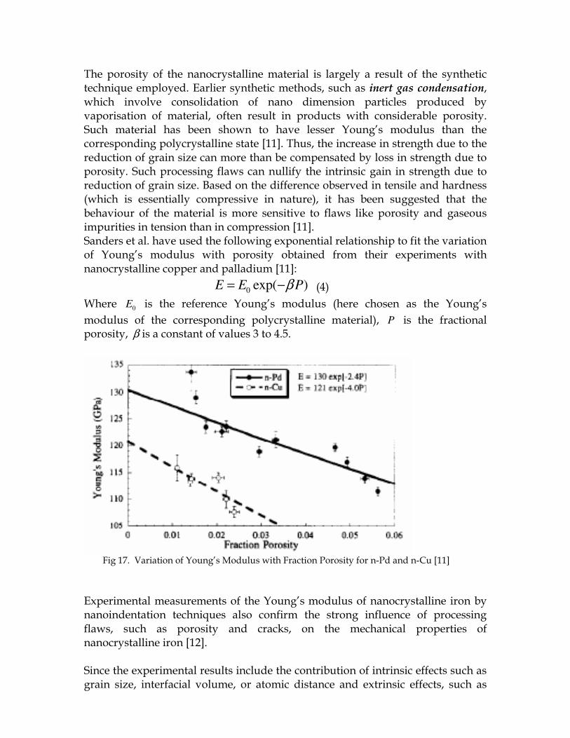
The porosity of the nanocrystalline material is largely a result of the synthetic technique employed. Earlier synthetic methods, such as inert gas condensation, which involve consolidation of nano dimension particles produced by vaporisation of material, often result in products with considerable porosity. Such material has been shown to have lesser Young’s modulus than the corresponding polycrystalline state [11]. Thus, the increase in strength due to the reduction of grain size can more than be compensated by loss in strength due to porosity. Such processing flaws can nullify the intrinsic gain in strength due to reduction of grain size. Based on the difference observed in tensile and hardness (which is essentially compressive in nature), it has been suggested that the behaviour of the material is more sensitive to flaws like porosity and gaseous impurities in tension than in compression [11]. Sanders et al. have used the following exponential relationship to fit the variation of Young’s modulus with porosity obtained from their experiments with nanocrystalline copper and palladium [11]:
0exp( )E E Pβ= − (4)
Where 0
E is the reference Young’s modulus (here chosen as the Young’s
modulus of the corresponding polycrystalline material), P is the fractional porosity, β is a constant of values 3 to 4.5.
Fig 17. Variation of Young’s Modulus with Fraction Porosity for n-Pd and n-Cu [11]
Experimental measurements of the Young’s modulus of nanocrystalline iron by nanoindentation techniques also confirm the strong influence of processing flaws, such as porosity and cracks, on the mechanical properties of nanocrystalline iron [12]. Since the experimental results include the contribution of intrinsic effects such as grain size, interfacial volume, or atomic distance and extrinsic effects, such as
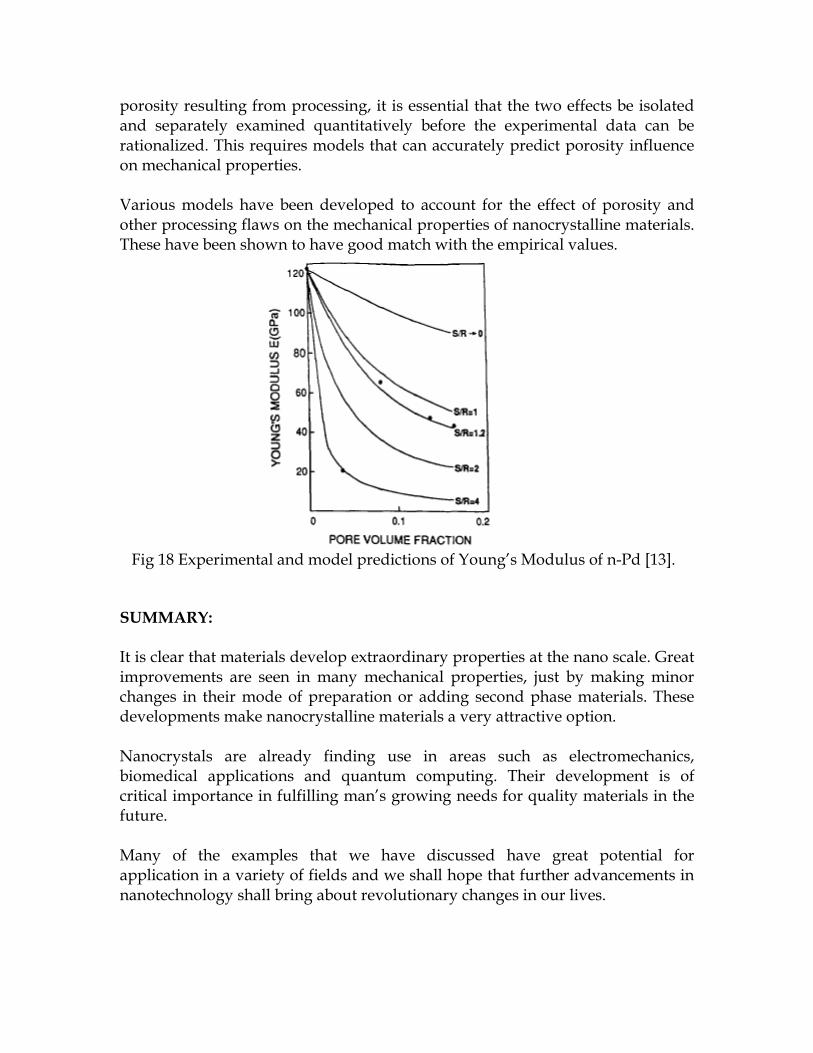
porosity resulting from processing, it is essential that the two effects be isolated and separately examined quantitatively before the experimental data can be rationalized. This requires models that can accurately predict porosity influence on mechanical properties. Various models have been developed to account for the effect of porosity and other processing flaws on the mechanical properties of nanocrystalline materials. These have been shown to have good match with the empirical values.
Fig 18 Experimental and model predictions of Young’s Modulus of n-Pd [13]. SUMMARY: It is clear that materials develop extraordinary properties at the nano scale. Great improvements are seen in many mechanical properties, just by making minor changes in their mode of preparation or adding second phase materials. These developments make nanocrystalline materials a very attractive option. Nanocrystals are already finding use in areas such as electromechanics, biomedical applications and quantum computing. Their development is of critical importance in fulfilling man’s growing needs for quality materials in the future. Many of the examples that we have discussed have great potential for application in a variety of fields and we shall hope that further advancements in nanotechnology shall bring about revolutionary changes in our lives.
References:
1. George E Dieter, Mechanical Metallurgy, McGraw –Hill, 1988.
2. Q. Wei , H.T. Zhang , B.E. Schuster , K.T. Ramesh , R.Z. Valiev ,L.J. Kecskes , R.J. Dowding , L. Magness , K. Cho (2006), Microstructure and mechanical properties of super-strong nanocrystalline tungsten processed by high-pressure torsion, Acta Materialia, 54 , 4079–4089. 3. Hans Conrad and Jagdish Narayan, (2000) On the grain size softening of nanocrystalline materials, Scripta Materialia, 42, 1025–1030. 4. M.A. Meyers, A. Mishra, D.J. Benson, (2006) Mechanical properties of nanocrystalline materials, Progress in Materials Science, 51, 427–556. 5. F.J. Hernández Guillén, Klemens Janischowsky, Joachim Kusterer, Wolfgang Ebert, Erhard Kohn, (2005) Mechanical characterization and stress engineering of nanocrystalline diamonds films for MEMS applications, Diamond & Related Materials, 14, 411– 415. 6. Yinmin Wang, Mingwei Chen, Fenghua Zhou, En Ma, (2002) High tensile ductility in a nanostructured metal, Nature, 419, 912-914. 7. Xinzhang Zhoua, Dustin M. Hulberta, Joshua D. Kuntza, Rajendra K. Sadangib, Vijay Shukla, Bernard H. Kear, Amiya K. Mukherjee, (2005) Superplasticity of zirconia–alumina–spinel nanoceramic composite by spark plasma sintering of plasma sprayed powders, Materials Science and Engineering A, 394, 353–359. 8. T.G. Nieh, J. Wadsworth, (2006) Homogeneous deformation of bulk metallic glasses, Scripta Materialia, 54, 387–392. 9. R.K. Guduru, R.O. Scattergood, C.C. Koch, K.L. Murty, S. Guruswamy, M.K. McCarter, (2006) Mechanical properties of nanocrystalline Fe–Pb and Fe–Al2O3, Scripta Materialia, 54, 1879–1883 10. Koteswararao V.Rajulapati, Ronald O.Scattergood, Korukonda L. Murty, Gerd Duscher and Carl C. Koch, (2006) Effect of Pb on the mechanical properties of nanocrystalline Al, Scripta Materialia, 55, 155–158. 11.P. G. Sanders, J. A. Eastman and J. R. Weertman ,(1997) Elastic and tensile behaviour of nanocrystalline copper and palladium, Acta Metallurgica, 45, 4019- 4025
12. G.E. Fougere, L. Riester, M. Ferber, J.R. Weertman, R.W. Siegel, (1995),Young's modulus of nanocrystalline Fe measured by nanoindentation, Materials Science and Engineering A204, 1- 6 13. V. Krstic , U. Erb and G. Palumbo ,(1993) Effect of porosity on Young’s Modulus of nanocrystalline materials, Scripta Metallurgica et Materialia, 29, 1501-1504
14. H. Gleiter, (1989) Nanocrystalline materials, Progress in Materials Science, 33, 223-315. 15.Hyoung Seop Kim and Mark B. Bush ,(1999)The Effect of Grain Size and Porosity on the Elastic Modulus of Nanocrystalline Materials, NanoStructured Materials, 11, 361–367