memory’packaging’challenges’ forthenewera’ · memory’packaging’challenges’...
TRANSCRIPT

© 2017 TechSearch International, Inc. © 2017 TechSearch International, Inc.
Memory Packaging Challenges for the New Era
E. Jan Vardaman, Founder and President

© 2017 TechSearch International, Inc. © 2017 TechSearch International, Inc.
Outline
• Mobile memory packaging trends • Wearable electronics • SSD trends and new non-‐volaGle memory • Memory for automoGve safety features • High-‐performance memory packaging trends • China joins the memory club
© 2017 TechSearch International, Inc. © 2017 TechSearch International, Inc.
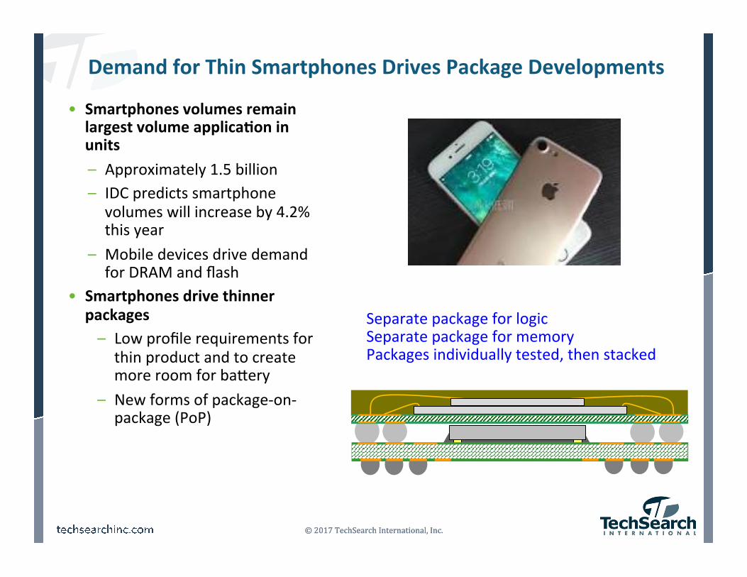
Demand for Thin Smartphones Drives Package Developments
• Smartphones volumes remain largest volume applicaGon in units – Approximately 1.5 billion – IDC predicts smartphone volumes will increase by 4.2% this year
– Mobile devices drive demand for DRAM and flash
• Smartphones drive thinner packages – Low profile requirements for thin product and to create more room for baIery
– New forms of package-‐on-‐package (PoP)
Separate package for logic Separate package for memory Packages individually tested, then stacked

© 2017 TechSearch International, Inc. © 2017 TechSearch International, Inc.
Qualcomm MDM9645M LTE X12 Modem
• Modem chip is flip chip bonded to substrate • Memory wire bonding on top
Source: TPSS.
Package size: 8.41 mm x 8.61 mm x 0.71 mm Modem chip: 6.14 mm x 5.45 mm x 0.098 mm Memory: 4.38 mm x 3. 7mm x 0.072 mm

© 2017 TechSearch International, Inc. © 2017 TechSearch International, Inc.
ApplicaGon Processor and Memory Packaging Trends • Thinner package and smaller footprint
– High-‐end smartphone ≤0.8mm package height • 3D IC with TSV provides the ulGmate in package height reducGon, but conGnues to be pushed out (thermal, cost, business issues)
• PoP in high-‐end smartphones – OpXon 1: ConXnue with FC on thin substrate – OpXon 2: Embedded AP in boIom laminate substrate
– OpXon 3: Fan-‐out WLP with applicaXon processor as boIom package and memory in top package
– OpXon 4: Some new format (RDL first/chip last) • Challenge is memory top package moving to finer ball pitch for packages – Requires pre-‐stack of memory on AP package
• FO-‐WLP AP in bo[om PoP for Apple’s A10 processor – Low profile – High rouXng density – Improved electrical and thermal performance
InFO is 20% thinner than FC-PoP

© 2017 TechSearch International, Inc. © 2017 TechSearch International, Inc.
3D IC Design: Thermal is CriGcal • Low-‐cost thermal management soluGons required for logic and memory stacking • Current PoP soluGon provides be[er thermal soluGon • Thermal issues: 3D circuits increase total power generated per unit surface area
– Chips in the stack may overheat of cooling is not provided – Space may be too small for cooling channels (very small gap for fluid flow) – Thinning chips creates extreme condiXons for on-‐chip hot spot – Need new low-‐power designs
Source: Renesas.

© 2017 TechSearch International, Inc. © 2017 TechSearch International, Inc.
Trends for Top PoP Memory Package
• Package-‐on-‐package (PoP) made up of logic in bo[om package and memory (typically >1 die) in top package
• Apple A10 PoP includes FO-‐WLP for bo[om package, four side-‐by-‐side memory wire bonded on laminate substrate for top PoP
• Future versions of top memory package could use FO-‐WLP
Source: eWiseTech.

© 2017 TechSearch International, Inc. © 2017 TechSearch International, Inc.
Amkor’s SWIFT™ High Yield FO-‐WLP with Chip Last
• Target applicaGons – Mobile – Networking
• Target device types – Baseband – ApplicaXon processor – Logic + memory
• UGlizes exisGng bump and assembly capability – MulX-‐die and large die capability as well as large package body size
– 3D format possible by stacking packages with Cu pillars or through molded via (TMV)
SWIFT™ Single Die Overmold
SWIFT™ 2 Die Overmold
SWIFT™ 2 Die Exposed
SWIFT™ 2 Die TMV PoP Overmold
SWIFT™ 2 Die Fan-in PoP
Source: Amkor.
© 2017 TechSearch International, Inc. © 2017 TechSearch International, Inc.
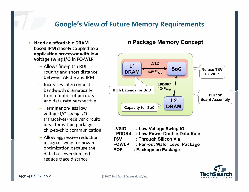
Google’s View of Future Memory Requirements
• Need an affordable DRAM-‐based IPM closely coupled to a applicaGon processor with low voltage swing I/O in FO-‐WLP
– Allows fine-‐pitch RDL rouXng and short distance between AP die and IPM
– Increases interconnect bandwidth dramaXcally from number of pin outs and data rate perspecXve
– TerminaXon-‐less low voltage I/O swing I/O transceiver/receiver circuits ideal for within package chip-‐to-‐chip communicaXon
– Allow aggressive reducXon in signal swing for power opXmizaXon because the data bus inversion and reduce trace distance
No use TSV FOWLP
POP or Board Assembly
LVSIO : Low Voltage Swing IO LPDDR4 : Low Power Double-Data-Rate TSV : Through Silicon Via FOWLP : Fan-out Wafer Level Package POP : Package on Package
L1 DRAM SoC
L2 DRAM Capacity for SoC
High Latency for SoC
LVSO
64Gbit/Sec
LPDDR4 12Gbit/Sec
In Package Memory Concept

© 2017 TechSearch International, Inc. © 2017 TechSearch International, Inc.
Wearables
• Health and fitness tracking bands including pedometers
• Watch products • System-‐in-‐Package (SiP) modules include
– ConnecXvity – Controller – Memory (Flash, SRAM, etc.) – MEMS
Source: Apple..

© 2017 TechSearch International, Inc. © 2017 TechSearch International, Inc.
Packages in Apple Watch Module
• Stacked die CSP for processor and memory packaging – Package height 0.56 mm – Processor solder bumped flip chip
– Memory wire bond • NAND flash memory stacked die CSP – Package height ~0.60 mm
Source: TPSS.
Stacked die CSP (logic boIom die, memory top die)

© 2017 TechSearch International, Inc. © 2017 TechSearch International, Inc.
Solid-‐State Drives Fueling Flash Demand
• External and Add-‐in Card SSD: – 1TB is popular high-‐capacity drive – Largest 2.5-‐inch drive in producXon is 16TB; 24TB and 32TB in future
• Embedded SSD (microSSD): – Up to 512GB in a single 16 mm x 20 mm BGA
• Boards or cards: – Single-‐ or double-‐sided – Generally have 1 to 8 NAND packages; Enterprise boards have as many as 32-‐40
– High-‐speed SSDs can also have a DRAM on board for caching
Source: Samsung, Anandtech.
Samsung 512GB BGA SSD: 16 x 48-layer MLC V-NAND (256Gb/die) 1 x ARM-based controller 1 x LPDDR4: 4Gb
Source: Storage Review.
Micron 2.4TB PCIe Enterprise SSD: 32 x 16nm MLC NAND (16 on each side) 1 x NVMe 16-channel controller 9 x 512Mb DRAM (5 on one side, 4 on other)

© 2017 TechSearch International, Inc. © 2017 TechSearch International, Inc.
Flash Memory Stack
• 3D Flash memory packaging – Wire bond for most cost effecXve soluXon – Everyone has a TSV demonstraXon vehicle – Cost has limited HVM applicaXon of flash with TSV stack some low-‐volume producXon expected to start this year for SSD
• Semiconductor process with stacked cells • New semiconductor non-‐volaGle memory development
Source: Samsung.
© 2017 TechSearch International, Inc. © 2017 TechSearch International, Inc.
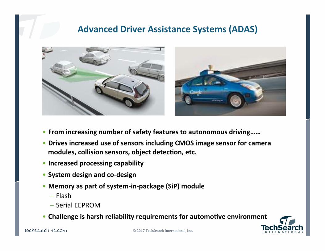
Advanced Driver Assistance Systems (ADAS)
• From increasing number of safety features to autonomous driving…… • Drives increased use of sensors including CMOS image sensor for camera modules, collision sensors, object detecGon, etc.
• Increased processing capability • System design and co-‐design • Memory as part of system-‐in-‐package (SiP) module
– Flash – Serial EEPROM
• Challenge is harsh reliability requirements for automoGve environment
© 2017 TechSearch International, Inc. © 2017 TechSearch International, Inc.
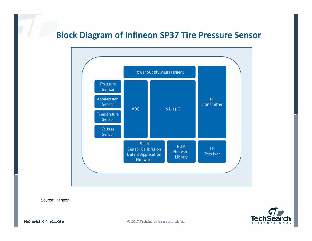
Block Diagram of Infineon SP37 Tire Pressure Sensor
Source: Infineon.

© 2017 TechSearch International, Inc. © 2017 TechSearch International, Inc.

© 2017 TechSearch International, Inc. © 2017 TechSearch International, Inc.
Renesas Module Sensor Fusion/ADAS Control ECU
• Results from radar and camera sensors are fused with vehicle acceleraGon, braking, and handling systems to avoid and reduce the possibility of accident in advance
• Modules include memory such as EEPROM • Future systems other applicaGons may use high bandwidth memory (HBM)

© 2017 TechSearch International, Inc. © 2017 TechSearch International, Inc.
High Performance Memory Stacks with TSV
• New memory architectures • Tezzaron high-‐speed memory
– ProducXon shipments – High-‐performance applicaXons
• Micron Hybrid Memory Cube (HMC) – Intel’s Knight’s Landing
• Samsung – DIMMS for servers – HBM (DRAM) stacks with TSVs
• SK Hynix – HBM on silicon interposer for GPU – Advantages include higher bandwidth, lower latency, and lower power consumpXon
Source: Samsung.
Source: SK Hynix.

© 2017 TechSearch International, Inc. © 2017 TechSearch International, Inc.
Samsung’s DDR4 with TSV
• Samsung’s 128GB RDIMM uses DDR4 memory with TSVs – DDR4 DRAMs fabricated on 20nm silicon node technology
• Targeted for Datacenters and Servers – Lower power – Double capacity of originally 64GB LRDIMM developed for Enterprise servers

© 2017 TechSearch International, Inc. © 2017 TechSearch International, Inc.
Lower Power ConsumpGon
• Lower Cio (0.4pF) and no terminaGon…small I/O current consumpGon • Lower speed per pin (1Gbps)… low power consumpGon
Source: SK Hynix.
© 2017 TechSearch International, Inc. © 2017 TechSearch International, Inc.
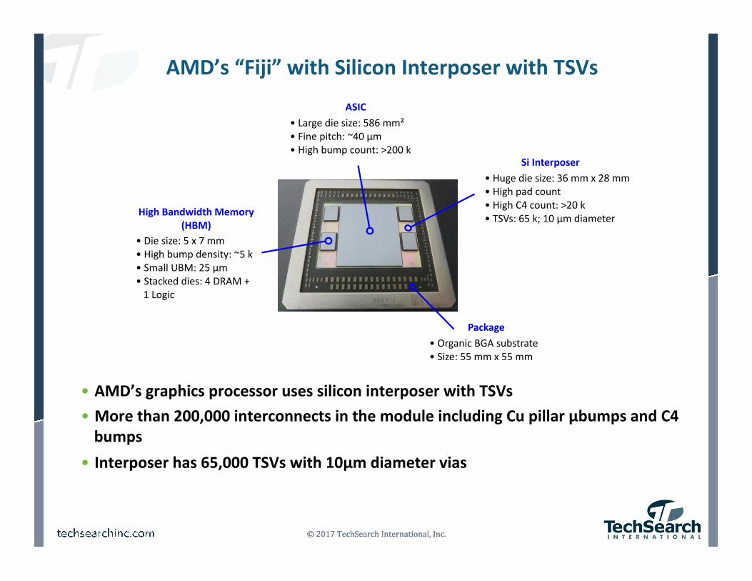
AMD’s “Fiji” with Silicon Interposer with TSVs
• AMD’s graphics processor uses silicon interposer with TSVs • More than 200,000 interconnects in the module including Cu pillar µbumps and C4 bumps
• Interposer has 65,000 TSVs with 10µm diameter vias
SiInterposer
HighBandwidthMemory(HBM)
ASIC
Package
•Largediesize:586mm²•Finepitch:~40µm•Highbumpcount:>200k
•OrganicBGAsubstrate•Size:55mmx55mm
•Diesize:5x7mm•Highbumpdensity:~5k•SmallUBM:25µm•Stackeddies:4DRAM+1Logic
•Hugediesize:36mmx28mm•Highpadcount•HighC4count:>20k•TSVs:65k;10µmdiameter

© 2017 TechSearch International, Inc. © 2017 TechSearch International, Inc.
AMD’s “Fiji” with Silicon Interposer and HBM
• AMD “Fiji” soluGon for the graphics market • Four HBM stacks, each containing stacked DRAMs and a logic die with TSVs mounted on the interposer
Source: AMD.

© 2017 TechSearch International, Inc. © 2017 TechSearch International, Inc.
Xilinx Products with Silicon Interposer
• Future products with HBM • Silicon interposer to handle communicaGon between HBM stack and FPGA
Source: Xilinx.
© 2017 TechSearch International, Inc. © 2017 TechSearch International, Inc.
Developing a Strong Memory Industry: Management Ma[ers
• Memory industry conGnues to move around the globe – US – Japan – Korea – Taiwan – China
• Development of memory industry requires more than just technology • Packaging developments will be key to memory success

© 2017 TechSearch International, Inc. © 2017 TechSearch International, Inc.
Conclusions
• Mobile devices (smartphones) drive unit volumes – Mobile DRAM – Flash memory
• Growth of SSDs driving flash memory volume growth • New non-‐volaGle memory developments • High performance compuGng lower volumes, but increasing use of high-‐performance memory with TSVs – DIMMs with TSV for increasing number of applicaXons – HBM on interposers – Performance is important, but cost is not irrelevant – Companies working on methods to lower cost of HBM
• Memory industry conGnues to evolve

TechSearch InternaXonal, Inc. 4801 Spicewood Springs Road, Suite 150
AusXn, Texas 78759 USA +1.512.372.8887
© 2017 TechSearch International, Inc.
Thank you!
TechSearch InternaXonal, Inc. 4801 Spicewood Springs Road, Suite 150
AusXn, Texas 78759 USA +1.512.372.8887
© 2017 TechSearch International, Inc.
Thank you!