mems based systems solutions - roger grace associates exactly is the problem?... and i think the...
TRANSCRIPT

The MEMS industry continues to grow but not everyone appears tounderstand its dynamics, assuming it to be similar to the dynamics of the semiconductor industry. This could not be further from the truth. Roger H. Grace, President of Roger Grace Associates discusses theMEMS report card and MEMS industry opportunities.
MEMS basedsystemssolutions:Thinkingoutside thechip
MICRONANOSYSTEMS 29
December 2008 / January 2009 www.micronanosystems.info
Most recently, a number of new “killerapplications” for MEMS have occurred.Traditionally, the automotive industry has
driven a number of significant large volume applications e.g.manifold absolute pressure sensors were the first, followed byairbag accelerometers. Tyre pressure monitoring (TPM) isexpected to provide significant opportunities for MEMS andMEMS-based systems providers. However, with the advent ofrapidly decreasing MEMS costs the consumer electronicsmarket has been the new “white knight” of the MEMS business.Portable handsets, MP3 players, digital cameras and gameshave been gobbling up large amounts of MEMS devicesincluding low-g accelerometers, microphones and gyros.
Even so with these new large volume opportunity recentlysurfacing, one might ask the question why has it taken so longfor MEMS to finally become commercialised. We haveconducted research in this area and addressed thecommercialisation timetable for a number of MEMS products(see Figure 1).
We have found that the mean time for commercialisation isaround 25 years from discovery to full commercialisation. Thefirst manifestation of MEMS was via the discovery of thepiezoresitive effect in Silicon by Charles Smith of Bell Labs withhis 1954 paper in Physical Review. In the more than 50 yearsthat have transpired, the MEMS industry has gone throughvarious bubbles, the most recent being the optical telecom one.
Where most analysts had projected rapidly expanding volume ofvarious MEMS-based optical components that would be theheart of the optical system, the market never was realised.Reviewing the various market research reports (including ours)we note that the MEMS market has been estimated to beapproximately $7 Billion US in 2008 while the semiconductordevice market has been estimated at over $200 Billion US. Oneasks why this significant discrepancy exists for technologiesthose were discovered within a mere 10 years of each other.
Roger Grace Associates has attempted to determine thereason for this and as a result has created a “MEMS IndustryReport Card” which first appeared in 1998.[1] The report cardhas tracked on a yearly basis the performance of the MEMSindustry vis-à-vis 14 critical success factors and assigned gradesfor each using a “Delphi” market research technique. Briefly,this technique uses a small selection of research experts (in ourcase it is approximately 55) from a worldwide data base thatrepresents users, suppliers of MEMS, materials and equipmentsuppliers and other MEMS infrastructure organisations e.g.foundries. Figure 2 presents the most recent report card for2007 (the 2008 report card is planned for March 2009).
Based on my involvement in conducting the many interviewsassociated with creating this report card, I believe some of themore important barriers to commercialisation of MEMS hasbeen the lack of adequate attention to design for manufacturingand test. The good news is that the grade for DfM&T has slowly
MNS Roger Grace v Final DR 18/12/08 15:12 Page 29

MICRONANOSYSTEMS30
www.micronanosystems.info December 2008 / January 2009
moved from a “C+” to a “B” in the past decade. However, Ibelieve that we still have a long way to go before the grade willattain an “A” status. I would like to address some of the reasonswhy this is so and provide some solutions that might be able toimprove the grade.
Alternately, the grade for infrastructure has moved from“C+” to “A-“. As such, the industry has done an excellent jobto provide MEMS manufacturers with the tools that they needto be able to be imminently successful, including design andanalysis software, MEMS wafer foundries, specialisedmanufacturing, test and metrology equipment and uniquematerials for MEMS.
The question therefore is if the resources are readily availablewhat exactly is the problem?... and I think the answer is in thelack of understanding of MEMS suppliers to develop solutionsthat are “outside the MEMS chip” and embody signalconditioning electronics, interconnects, networking capabilities,energy sources and most importantly…packaging and asembly. Isuggest that MEMS “device” e.g. accelerometers, pressuresensors suppliers need to take a more systems level approach toproviding their customers with the best possible solution andcustomers need to understand the limitations and capabilities aswell as the cost and time to market of developing a systems levelapproach. The outcome of this approach will be to havemanufacturers establish better product differentiation and addvalue (and profit margin) rather than fight it out in acommoditised market which stresses price.
The heart of the problemIn our research to determine the root cause of the problem, wehave come up with a couple of possible answers. With rareexception, most of the “pioneers” that have helped create thisindustry have come from extensive academic backgrounds andhas a specialty in “electrical engineering” which typically has afocus on circuits. Their thesis topics were device oriented and
many have started their companies on work that was groundedon projects undertaken as graduate students.
However, Professor Khalil Najafi, recently appointedchairman of the Electrical Engineering and Computer ScienceDepartment of the University of Michigan and Deputy Directorof the National Science Foundation’s Wireless IntegratedMicrosystems Center (WIMS) said, “We have a history datingback to 1988 with our implantable micro neural stimulator ofmaking the packaging of MEMS a very important topic. In themid 90’s, we had two students who did their Ph. D. thesis onMEMS packaging, by 2000 we had 5 and now we have 9. Thisconstitutes approximately 20% of our current total of Ph.D.’sand post-docs.” Other universities have also focused on MEMSpackaging including the University of Colorado and GeorgiaTech. Another is that packaging is not very “exciting” and wasperceived as a given or a “let’s use a standard semiconductorpackage”. In addition, most smaller MEMS companies did nothave the resources to have a broad selection of experts on staffto create an in-depth multi-disciplinary system solutionapproach…they were satisfied with creating the MEMS chipand let their customer solve the integration, interfacing,packaging and assembly challenges.
Finally, to design a MEMS device is a very complicatedprocess. Although there are numerous design softwareprogrammes available to MEMS designers, the complexities ofchip design and package and media interaction tend to strap allbut the larger MEMS suppliers…therefore these less resourcedcompanies need to focus on the chip design to be able to survive.
However, a number of research institutes and universities arefocusing their efforts on these MEMS-based systems solutions.These companies include, Fraunhofer Einrichtung, Electronische,Nanosysteme Institute ( Chemnitz, Germany); IMEC (Belgium);Infotonics (US), University of Texas Arlington’s Automation andRobotics Research Institute (ARRI) and the University ofMichigan WIMS .
I have proposed a “MEMS-based system solutions” approach as aviable vehicle for current MEMS device producers and future MEMSdevice producers and to encourage them to “think outside the chip”
Figure 1: MEMS Commercialization Timetable shows onaverage that various MEMS products take approximately25 years from discovery to full commercialization
Figure 2: 2007 MEMS Industry Report Card uses fourteencritical success factors to assess the progress of MEMScommercialization over the last decade
MNS Roger Grace v Final DR 18/12/08 15:12 Page 30

MICRONANOSYSTEMS 31
December 2008 / January 2009 www.micronanosystems.info
So what is this MEMS based solution?I have proposed a “MEMS-based system solutions” approach asa viable vehicle for current MEMS device producers and futureMEMS device producers and to encourage them to “thinkoutside the chip”. I am not attempting to diminish theimportance of the MEMS device but rather discuss the need ofadopting a systems approach to solving the application whichincludes as a core the MEMS device(s) in addition to multipleelectronic circuit devices, interconnects, packaging andassembly. All of these elements plus testing must be a part ofthe system architecture addressed in the initial solution design.In the annual METRIC workshop in March 2008 sponsored bythe MEMS Industry Group (MIG), this year’s topic waspackaging. The outcome of the panel discussions was that theyconsidered the inability of the early consideration of packagingissues and tradeoffs to pose a major problem in the finalMEMS-based solution. Our independent research has alsocorroborated this MIG finding.
A key element in the MEMS-based solution is the signalconditioning circuit. The output signal of a MEMS device needsa great deal of enhancement and modification to be useable in asystem. The inclusion of this device has been widely adopted andin different forms. Some companies have decided to create aMEMS device with an integrated/monolithic signal conditioningcircuit e.g. Analog Devices ADXL accelerometer product lineand Akustica’s MEMS microphone whereas most companieshave take a heterogeneous/multi chip approach e.g. Freescale,Kionix, STMicroelectronics, VTI , accelerometers and AnalogDevices, Pulse/Sonion, and Wolfson microphones.
The decision on which approach to take is a complex processthat is driven by non recurring engineering costs, unit costs,volumes, time to market, packaging/interconnectivity issues toname a few. The decision as to how to source the signalconditioning IC is dependent on the internal resources of theMEMS device developers. Analog Devices and Freescale aremajor IC suppliers and it is a natural for them to design andmanufacture these signal conditioning IC’s. Some companieslike Kionix have in-house design capability to design the ICs anduse a foundry to manufacture them. Many companies who lackthe expertise and resources to have their own in-house signalconditioning team use companies including AustriaMicrosystems, Si Ware Systems design the signal conditioningICs and in the case of Austria Microsystems, to alsomanufacture the devices in- house. Functions including analogueto digital conversion, amplification, filtering, comparators,temperature sensors and E2PROM are popular functions.
It is important to note that embedded software is a verycritical part of the signal conditioning strategy. The judicioususe of this function can create high performance solutions usingadditional temperature sensor inputs and E2PROM to optimallycompensate the MEMS device over temperature. In addition,algorithms can be used to compensate for device manufacturingvariances as well as to introduce highly functional solutions thatcan deliver functions including self-test, power management,control logic and ESD protection.
Packaging, interconnects and assemblyPackaging, interconnecting and assembly of the solutionelements is perhaps the most important and critical part of thesystem solution concept. It is well known and accepted the costof packaging/interconnects, test and assembly are a major
percentage of the total cost of the solution. Karen Lightman,Managing Director of MIG said, “In our industry report, Focuson MEMS Packaging[2] , that was created as a result of ourrecent annual METRIC conference, we reported that the cost ofthe package for a MEMS device can be 30-40% of the totalcost of the entire device. When testing and packaging are bothconsidered, the consensus of the METRIC’s working groups isthat the cost may reach 70% of the total device cost. Byimplementing and conforming to standard CMOS processes,companies can reduce cost, as packaging and testing compriseonly 10-15% of the total device cost”. In the generalmicroelectronic area, packaging of ICs is more of an issue ofusing standard packages, MEMS packaging tends to be moreapplication specific. The old mantra of “one product/oneprocess” has been added to by “one product/one package” forMEMS asserting MEMS application specific nature.
“Packaging is critical for product success” says NancyStoffel, Director of the Microsystems Packaging at Infotonics.“Not only is it a main cost element but it dictates time tomarket and system performance. The package providesinterconnections for electrical, fluidic, optical and thermalinputs. It protects the MEMS fragile structure against particles,humidity, vibration and stress while providing controlled
Figure 3: Multiple MEMS sensors and fluidic devices workwith signal conditioning circuitry, associatedinterconnects and hermetic packaging to create anintegrated MEMS-based systems solution
Figure 4: MEMS-based system for telecom apps with alower die which supports an array of MEMS switches andhas a wafer-level cap. On top of this is a CMOS controllerdie with wire bonding connecting the CMOS to MEMS die.
Ima
ge
co
urt
sey
of
Asp
en
Te
ch
no
log
ies
Ima
ge
co
urt
sey
of
Un
ive
rsit
y o
f M
ich
iga
n,
WIM
S
MNS Roger Grace v Final DR 18/12/08 15:12 Page 31

MICRONANOSYSTEMS32
www.micronanosystems.info December 2008 / January 2009
environmental requirements including vacuum and hermeticity.Finally it enables precision placement and alignment relative toother devices and connections in the system” she added.
WIMS Najafi in his seminal 2003 paper, “MicropackagingTechnologies for Integrated Microsystems: Application toMEMS and MOEMS”[3] stated that “there are several keytechnological challenges to the packaging of MEMS and theycan be categorised under three general topics: 1. MEMS deviceencapsulation(protection), connection and assembly (Fig 3).There are many reasons for this chief amongst these being thatmost MEMS devices work in a multi-domained fashion i.e.electro-mechanical, electro-chemical, electro-optical whereas ICdevices typically work in a pure electronic domaine.
MEMS packages not only need to withstand shock, vibration,moisture but to work properly, they must be immersed in theenvironment that they need to measure e.g. a blood pressuresensor or an oil pressure sensor. These media are chemicallyharsh and the MEMS device must be physically isolated fromthe media while still maintaining the ability to be in contactwith it…and this is not a paradox!
“MEMS packaging must be designed to encapsulate andprotect the MEMS (and other system components) while engagethe device with the media that it must measure” stated EricLeonard, a packaging consultant who chaired a packaging panelat the MIG METRIC conference. ‘In addition, the package mustbe designed NOT to interact with the MEMS device and impartstresses to it which will affect its performance especially overlarge temperature ranges. The package thus must be rugged andbe designed in a cost-effective fashion.’
There are a number of commercial packaging house availableto support MEMS device developers. On one side we have theclassical semiconductor packaging houses who tend to want towork with companies that can use standard semiconductor
packages e.g. SSOP, QFN, QFP including Amcor, ASE,Boschman, Carsem and UTAC. In addition, a number ofcompanies specialising in MEMS packaging exist includingAspen Technologies, ePack, and Microassembly Technologies. Aswe noted earlier, a thoroughly adequate infrastructure exists tosupport the packaging of MEMS-based systems solutions fromprototyping to large scale production.
Having said this, what are the innovative and uniquetechnologies that are being developed to overcome thispackaging challenge? I believe some of the more significant are3-D die stacking, through hole vias (THV) and wafer levelpackaging (WLP).
3-D die stacking is becoming quite popular both in the IC andMEMS area. The use of this approach minimises used area onthe substrate/board on which the MEMS die is mounted.However, once the MEMS chips and its signal conditioning chipare stacked, one has to provide connections for these devices.Some use the technique of external bond wires as is illustratedin Fig 4 which shows Aspen Technologies approach to mountingan optical MEMS chip to a CMOS controller chip.
More recently, through hole vias are becoming the technologyof choice. It is interesting to note that in the research to writethis article, we uncovered that “ THV’s were used in the SCAP(Silicon Capacitive Absolute Pressure) sensor designed andmanufactured by Ford in the early 80’s using a laser to createthe holes in the glass that were subsequently metalised and thatcapped the sensor” stated Joe Giachino, Former Ford sensordesigner and currently External Programmes Director of theUniversity of Michigan WIMS. Here is a situation whereMEMS technology has been adopted by the IC industry.
Chip Spangler, VP and CTO at Aspen Technologies said, “Thesynergy between thin electronics, wafer level packaging andthrough-hole vias allowing die stacking to become mainstream isnow underway and has been driven by MEMS adoption intoportable electronics. This technology has its root in MEMS”.Note: Spangler did early work on the Ford SCAP while agraduate student at UMICH. Through hole vias are typicallyvertical but startup ePack is providing both traditional verticalas well as lateral vias. The lateral polysilicon feed throughapproach can be used in CMOS and used a low temperature(200 degrees C) LPCVD process. This approach is presently
Fig 6: The five layer microfluidic device is used for DNAamplification and has layers of etched Silicon and patternedpolymer layers joined together using a submicron thick adhesive
Figure 5: In-situ adhesive wafer bonding of glass waferswith micro lenses. The bond is performed in a maskaligner with the adhesive being cured by ultra violetradiation
Ima
ge
co
urt
sey
of
Info
ton
ics
Ima
ge
co
urt
sey
of
SUSS
Mic
roTe
c
MNS Roger Grace v Final DR 18/12/08 15:12 Page 32
MICRONANOSYSTEMS 33
December 2008 / January 2009 www.micronanosystems.info
being used in a wide range of devices including accelerometersand RF switches.
Wafer level packaging (WLP) using various bondingtechniques is another technology that started as a MEMStechnology. Currently, it is one of the hottest technologies inboth the IC and MEMS areas. Wafer bonding process optionsinclude fusion, plasma activated fusion, anodic, thermo-compression, eutectic, glass-frit and adhesive. Infotonics uses avery sophisticated adhesive bonding strategy to create a fivelevel wafer stack for a micro-fluidic device.[4] Adhesive bondingtechniques are popular when then can be conducted in a batchmode at room temperature. Suss Mictotec has developed atechnique where it spins the adhesive on to glass or Si wafer anduse standard mask alignment techniques with accuracies of lessthan 1 micron wafer to wafer. Ultra violet radiation is used tocure the adhesive. The resulting process is benign and does notdeform heat sensitive optical elements while maintaining highthroughput and low unit cost as a result of its wafer scaleformat (Fig 6). Its selection was based on a number of factorsincluding forgiveness of surface non-uniformities, low pressure(75 psi) and low temperature (170 degree C) application.
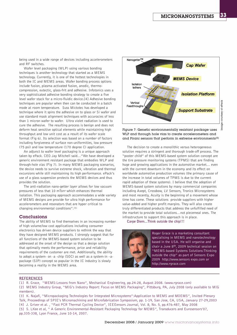
An adjunct to wafer level packaging is a unique approachtaken by ePack. CEO Jay Mitchell said…”We have developed ageneric environment resistant package that embodies WLP andthrough-hole vias (Fig 7). In many MEMS packaging scenarios,the device needs to survive extreme shock, vibration and thermalexcursions while still maintaining its high performance. ePack’suse of a glass suspension protects the MEMS devices and thusprovides the solution.
The anti-radiation nano-getter layer allows for low vacuumpressures of less that 10 mTorr which enhances thermalisolation. This packaging approach accommodates a wide varietyof MEMS designs are provide for ultra high performance foraccelerometers and resonators that are hyper critical tochanging environmental conditions”.[5]
ConclusionsThe ability of MEMS to find themselves in an increasing numberof high volume/low cost applications including consumerelectronics has driven device suppliers to rethink the way thatthey have designed MEMS products. I strongly suggest that forall functions of the MEMS-based system solution to beaddressed at the onset of the design so that a design solutionthat optimally meets the performance, price and reliabilityrequirements of the customer are met. Additionally, the abilityto adopt a system- on -a -chip (SOC) as well as a system-in –a-package (SIP) concept so popular in the IC industry is slowlybecoming a reality in the MEMS area.
The decision to create a monolithic versus heterogeneoussolution requires a stringent and thorough trade-off process. The“poster child” of this MEMS-based system solution concept arethe tire pressure monitoring systems (TPMS) that are findinghuge and growing applications in the automotive market… evenwith the current downturn in the economy and its effect onworldwide automotive production volumes (the primary cause ofthe increase in total volumes of TPMS is due to the currentrapid adoption of these systems). I believe that the adoption ofMEMS-based system solutions by many commercial companiesincluding Axept, Crossbow, LV Sensors, Tronics Microsystemsand most recently, Acuity is the beginning of a movement whosetime has come. These solutions provide suppliers with highervalue-added and higher profit margins. They will also createtruly differentiated products that address the unfulfilled need ofthe market to provide total solutions…not piecemeal ones. Theinfrastructure to support this approach is in place.
Carpe Diem...Think outside the chip!!!
Roger Grace is a marketing consultantspecialising in MEMS and nanotechnologybased in the USA. He will organise andchair a June 8th, 2009 technical session on“MEMS-based Systems Solutions:Thinkingoutside the chip” as part of Sensors Expo2009 http://www.sensors expo.com orhttp://www.rgrace.com
Figure 7: Genetic environmentally resistant package usesWLP and through hole vias to create accelerometers andand Pirani sensors that perform in extreme environments[5]
REFERENCES[1] R. Grace, “MEMS:Lessons from Nano”, Mechanical Engineering, pp.24-28, August 2008. (www.rgrace.com)[2] MEMS Industry Group, “MIG’s Industry Report: Focus on MEMS Packaging”, Pittsburg, PA, July 2008 (only available to MIGmembers).[3] K. Najafi, “Micropackaging Technologies for Integrated Microsystems”:Application to MEMS and MOEMS”, Invited PlenaryTalk, Proceedings of SPIE’s Micromachining and Microfabrication Symposium, pp. 1-19, San Jose, CA, USA, January 27-29,2003[4] J. Griver et al. , “Fast PCR Thermal Cycling Device”, IEEEensors Journal, Vol. 8, No. 5, pp.476-487, May 2008[5] S. LKee et al, “ A Generic Environmental-Resistant Packaging Technology for MEMS”, Transducers and Eurosensors’07,pp.335-338, Lyon France, June 10-14, 2007.
Ima
ge
co
urt
sey
of
ePa
ck
MNS Roger Grace v Final DR 18/12/08 15:12 Page 33