methodology and implementation hongtu jiang lund 2007
TRANSCRIPT

Design Issues in VLSI Implementation of
Image Processing Hardware Accelerators
Methodology and Implementation
Hongtu Jiang
Lund 2007

Department of ElectroscienceLund UniversityBox 118, S-221 00 LUNDSWEDEN
This thesis is set in Computer Modern 10pt,with the LATEX Documentation Systemon 100gr Colortech+TM paper.
No. 66ISSN 1402-8662
c© Hongtu Jiang January 2007

Abstract
With the increasing capacity in today’s hardware systems enabled by technol-ogy scaling, image processing algorithms with substantially higher complexitycan be implemented on a single chip enabling real-time performance. Com-bined with the demand for low power consumption or larger resolution seenin many applications such as mobile devices and HDTV, new design method-ologies and hardware architectures are constantly called for to bridge the gapbetween designers productivity and what the technology can offer.
This thesis tries to address several issues commonly encountered in theimplementations of real-time image processing system designs. Two imple-mentations are presented to focus on different design issues in hardware designfor image processing systems.
In the first part, a real-time video surveillance system is presented by com-bining five papers. The segmentation unit is part of a real-time automatedvideo surveillance system developed at the department, aiming for trackingpeople in an indoor environment. Alternative segmentation algorithms areelaborated, and various modifications to the selected segmentation algorithmis made aiming for potential hardware efficiency. In order to bridge the mem-ory bandwidth issue which is identified as the bottleneck of the segmentationunit, combined memory bandwidth reduction schemes with pixel locality andwordlength reduction are utilized, resulting in an over 70% memory bandwidthreduction. Together with morphology, labeling and tracking units developedby two other Ph.D. students, the whole surveillance system is prototyped onan Xilinx VirtexII pro VP30 FPGA, with a real-time performance at a framerate of 25 fps with a resolution of 320× 240.
For the second part, two papers are extended to discuss issues of a con-troller design and the implementation of control intensive algorithms. To avoidtedious and error prone procedure of hand coding FSMs in VHDL, a controllersynthesis tool is modified to automate a controller design flow from C-like con-trol algorithm specification to controller implementation in VHDL. To addressissues of memory bandwidth as well as power consumptions, a three level ofmemory hierarchy is implemented, resulting in off-chip memory bandwidth re-duction from N2 per clock cycle to only 1 per pixel operation. Furthermore,potential power consumption reduction of over 2.5 times can be obtained withthe architecture. Together with a controller synthesized from the developedtool, a real-time image convolution system is implemented on an Xilinx Vir-texE FPGA platform.
iii

Contents
Abstract iii
Contents v
Preface vii
Acknowledgment ix
List of Acronyms xi
General Introduction 1
1 Overview 3
1.1 Thesis Contributions . . . . . . . . . . . . . . . . . . . . . . . . . 3
1.2 Thesis Outline . . . . . . . . . . . . . . . . . . . . . . . . . . . . 4
2 Hardware Implementation Technologies 7
2.1 ASIC vs. FPGA . . . . . . . . . . . . . . . . . . . . . . . . . . . 7
2.2 Image Sensors . . . . . . . . . . . . . . . . . . . . . . . . . . . . 12
2.3 Memory Technology . . . . . . . . . . . . . . . . . . . . . . . . . 15
2.4 Power Consumption in Digital CMOS technology . . . . . . . . . 22
v

Hardware Accelerator Design of an AutomatedVideo Surveillance System 30
1 Segmentation 33
1.1 Introduction . . . . . . . . . . . . . . . . . . . . . . . . . . . . . 331.2 Alternative Video Segmentation Algorithms . . . . . . . . . . . . 341.3 Algorithm Modifications . . . . . . . . . . . . . . . . . . . . . . . 461.4 Hardware Implementation of Segmentation Unit . . . . . . . . . . 531.5 System Integration and FPGA Prototype . . . . . . . . . . . . . . 711.6 Results . . . . . . . . . . . . . . . . . . . . . . . . . . . . . . . . 721.7 Conclusions . . . . . . . . . . . . . . . . . . . . . . . . . . . . . 73
2 System Integration of Automated Video Surveillance System 75
2.1 Introduction . . . . . . . . . . . . . . . . . . . . . . . . . . . . . 772.2 Segmentation . . . . . . . . . . . . . . . . . . . . . . . . . . . . 782.3 Morphology . . . . . . . . . . . . . . . . . . . . . . . . . . . . . 852.4 Labeling . . . . . . . . . . . . . . . . . . . . . . . . . . . . . . . 882.5 Feature extraction . . . . . . . . . . . . . . . . . . . . . . . . . . 902.6 Tracking . . . . . . . . . . . . . . . . . . . . . . . . . . . . . . . 902.7 Results . . . . . . . . . . . . . . . . . . . . . . . . . . . . . . . . 912.8 Conclusions . . . . . . . . . . . . . . . . . . . . . . . . . . . . . 93
Controller Synthesis in Real-time Image Con-volution Hardware Accelerator Design 99
1 Introduction 103
1.1 Motivation . . . . . . . . . . . . . . . . . . . . . . . . . . . . . . 1031.2 FSM Encoding . . . . . . . . . . . . . . . . . . . . . . . . . . . . 1051.3 Architecture Optimization . . . . . . . . . . . . . . . . . . . . . . 1071.4 Memories and Address Processing Unit . . . . . . . . . . . . . . . 1101.5 Conclusion . . . . . . . . . . . . . . . . . . . . . . . . . . . . . . 110
2 Controller synthesis in image convolution hardware accelerator de-
sign 113
2.1 Introduction . . . . . . . . . . . . . . . . . . . . . . . . . . . . . 1132.2 Two dimensional image convolution . . . . . . . . . . . . . . . . 1142.3 Controller synthesis . . . . . . . . . . . . . . . . . . . . . . . . . 1182.4 Results . . . . . . . . . . . . . . . . . . . . . . . . . . . . . . . . 1202.5 Conclusions . . . . . . . . . . . . . . . . . . . . . . . . . . . . . 121

Preface
This thesis summarizes my academic work in the digital ASIC group at the de-partment of Electroscience, Lund University, for the Ph.D. degree in circuit design.The main contribution to the thesis is derived from the following publications:
H. Jiang and V. Owall, “FPGA Implementation of Real-time Image Convo-lutions with Three Level of Memory Hierarchy,” in IEEE conference on FieldProgrammable Technology (ICFPT), Tokyo, Japan, 2003.
H. Jiang and V. Owall, “FPGA Implementation of Controller-Datapath Pairin Custom Image Processor Design,” in IEEE International Symposium onCircuits and Systems (ISCAS), Vancouver, Canada, 2004.
H. Jiang, H. Ardo and V. Owall, “Hardware Accelerator Design for Video Seg-mentation with Multi-modal Background Modeling,” in IEEE InternationalSymposium on Circuits and Systems (ISCAS), Kobe, Japan, 2005.
F. Kristensen, H. Hedberg, H. Jiang, P. Nilsson and V. Owall, “HardwareAspects of a Real-Time Surveillance System,” in European Conference onComputer Vision, Graz, (ECCV), Graz, Austria, 2006.
H. Jiang, H. Ardo and V. Owall, “Real-time Video Segmentation with VGAResolution and Memory Bandwidth Reduction,” in IEEE International Con-ference on Advanced Video and Signal based Surveillance (AVSS), Sydney,Australia, 2006.
H. Jiang, H. Ardo and V. Owall, “VLSI Architecture for a Video Segmen-tation Embedded System with Algorithm Optimization and Low MemoryBandwidth,” To be Submitted to IEEE Transactions on Circuits and Sys-tems for Video Technology, February, 2007.
F. Kristensen, H. Hedberg, H. Jiang, P. Nilsson and V. Owall, “Working title:Hardware Aspects of a Real-Time Surveillance System,” To be submitted toSpringer Journal of VLSI Signal Processing Systems for Signal, Image, andVideo Technology, February, 2007.
vii


Acknowledgment
First of all, I would like to thank my supervisor, Viktor Owall, for all the helpand encouragement during all these years of my graduate study. His knowledge,inspiration and efforts to explain things clearly has a deep impact on my researchwork in Digital IC design. I can not imagine the completion of my thesis workwithout his help. I would also like to thank him for his eternal attempts to get meambitious, and his strong intentions to get me addictive to sushi and beer whenwe were traveling in Canada and Japan.
I would also like to thank Thomas, for all the fruitful discussions that were ofgreat help to the project developments. I learned lots of practical design techniquesduring our discussions. I would also like to thank Anders for the suggestions on myproject work when I started here. Many thanks to Zhan, who gave me inspirationsand deep insights into Digital IC design and many other things.
I am also grateful to Fredrik for reading parts of the thesis, and Matthias, Hugo,Joachim, Erik ,Henrik, Johan, Deepak, Martin, Peter for the many interestingconversations and help. I really enjoy working in the group.
I would like to extend my gratitude to the colleagues and friends at the de-partment. I would like to thank Jiren for introducing me here, Kittichai for all theenjoyable conversations and help, Erik for helping me with the computers and allkinds of relevant or irrelevant interesting topics, Pia, Elsbieta and Lars for theirmany assistance.
I would also like to thank Vinnova Competence Center for Circuit Design(CCCD) for financing the projects, Xilinx for donating FPGA boards and Axisfor their network camera and expertise on image processing. Thanks to Depart-ment of Mathematics for their input on the video surveillance project, especiallyHakan Ardo who gave me many precious advices.
Finally, I would like to thank my parents, my sister and my nephew, who supportme all the time, and my wife Alisa and our daughter Qinqin, who bring me loveand lots of joy.
ix


List of Acronyms
ADC Analog-to-Digital Converter
ASIC Application-Specific Integrated Circuit
Bps Bytes per second
CCD Charge Coupled Device
CCTV Closed Circuit Television
CFA Color Filter Array
CIF Common Intermediate Format
CMOS Complementary Metal Oxide Semiconductor
CORDIC Coordinate Rotation Digital Computer
DAC Digital-to-Analog Converter
DCM Digital Clock Manager
DCT Discrete Cosine Transform
DWT Discrete Wavelet Transform
DDR Double Data Rate
DSP Digital Signal Processor
FD Frame Difference
FIFO First In, First Out
FIR Finite Impulse Response
FPGA Field Programmable Gate Array
fps frames per second
FSM Finite State Machine
HDL Hardware Description Language
IIR Infinite Impulse Response
xi

IP Intellectual Property
kbps kilo bits per second
KDE Kernel Density Estimation
LPF Linear Predictive Filter
LSB Least Significant Bit
LUT Lookup Table
Mbps Mega bits per second
MCU Micro-Controller Unit
MoG Mixture of Gaussian
MSB Most Significant Bit
PPC Power PC
P&R Place and Route
RAM Random-Access Memory
RISC Reduced Instruction Set Computer
PCB Printed Circuit Board
ROM Read-Only Memory
SRAM Static Random-Access Memory
SDRAM Synchronous Dynamic Random-Access Memory
SoC System on Chip
VGA Video Graphics Array
VHDL Very High-level Design Language
VLSI Very Large-Scale Integration

General Introduction
1

Chapter 1
Overview
Imaging and video applications are one of the fastest growing sectors of themarket today. Typical application areas include e.g. medical imaging, HDTV,digital cameras, set-top boxes, machine vision and security surveillance. Asthe evolution in these applications progresses, the demands for technology in-novations tend to grow rapidly over the years. Driven by the consumer elec-tronics market, new emerging standards along with increasing requirementson system performance imposes great challenges on today’s imaging and videoproduct development. To meet with the constantly improved system perfor-mance measured in, e.g., resolution, throughput, robustness, power consump-tion and digital convergence (where a wide range of terminal devices must pro-cess multimedia data streams including video, audio, GPS, cellular, etc.), newdesign methodologies and hardware accelerator architectures are constantlycalled for in the hardware implementation of such systems with real-time pro-cessing power. This thesis tries to deal with several design issues normallyencountered in hardware implementations of such image processing systems.
1.1 Thesis Contributions
In this thesis, implementation issues are elaborated regarding transformingimage processing algorithms into hardware realizations in an efficient way. Withthe major concern to address memory bottlenecks which are common to mostimage applications, architectural considerations as well as design methodologyconstitute the main scope of the thesis research work. Two implementationsare contributed in the thesis for the design of image processing accelerators:
3

4 CHAPTER 1. OVERVIEW
In the first implementation, a real-time video segmentation unit is imple-mented on an Xilinx FPGA platform. The segmentation unit is part of a real-time embedded video surveillance system developed at the department, whichare aimed to track people in an indoor environment. Alternative segmenta-tion algorithms are elaborated, and an algorithm with Mixture of Gaussianapproach is selected based on the trade-offs of segmentation quality and com-putational complexity. For hardware implementation, memory bottlenecks areaddressed with combined memory bandwidth reduction schemes. Modificationsto the original video segmentation are made to increase hardware efficiency.
In the second implementation, a synthesis tool is modified to automate acontroller design flow from a control algorithm specification to VHDL imple-mentation. The modified tool is utilized in the implementation of a real-timeimage convolution accelerator, which is prototyped on an Xilinx FPGA. Anarchitecture of three levels of memory hierarchy is developed in the image con-volution accelerator to address issues of memory bandwidth and power con-sumption.
1.2 Thesis Outline
The thesis is structured into three parts. The introduction part covers topicsconcerning a range of technologies used in the hardware implementation of atypical image processing systems, e.g. image sensors, signal processing units,memory technologies and displays. Comparisons are made in various technolo-gies regarding performance, area and power consumption cost etc. Followingthe introduction are two parts covering implementations by the author withthe aim of different design goals.
Part I
A design and implementation of a real-time video surveillance system ispresented in this part. Details on video segmentation implementation fromalgorithm evaluation to the architecture and hardware design are elaborated.Novel ideas of how off-chip memory bandwidth can be reduced by utilizingpixel locality and wordlength reduction scheme are shown. Modifications tothe existing Mixture of Gaussian (MoG) [1] is proposed aiming for potentialhardware efficiency. The implementation of the segmentation unit is based on:
H. Jiang, H. Ardo and V. Owall, “Hardware Accelerator Design for VideoSegmentation with Multi-modal Background Modeling,” in IEEE Inter-national Symposium on Circuits and Systems (ISCAS), Kobe, Japan,2005.
H. Jiang, H. Ardo and V. Owall, “Real-time Video Segmentation with

1.2. THESIS OUTLINE 5
VGA Resolution and Memory Bandwidth Reduction,” in IEEE Inter-national Conference on Advanced Video and Signal based Surveillance(AVSS), Sydney, Australia, 2006.
H. Jiang, H. Ardo and V. Owall, “VLSI Architecture for a Video Segmen-tation Embedded System with Algorithm Optimization and Low MemoryBandwidth,”To be Submitted to IEEE Transactions on Circuits and Sys-tems for Video Technology, February, 2007.
The second chapter of the part is dedicated to system integration of thesegmentation into a complete tracking system, which includes segmentation,morphology, labeling and tracking. The complete system is implemented on anXilinx VirtexII pro FPGA platform with real-time performance at a resolutionof 320 × 240. The implementation of the complete embedded tracking systemis based on:
F. Kristensen, H. Hedberg, H. Jiang, P. Nilsson and V. Owall, “HardwareAspects of a Real-Time Surveillance System,” in European Conference onComputer Vision, Graz, (ECCV), Graz, Austria, 2006.
F. Kristensen, H. Hedberg, H. Jiang, P. Nilsson and V. Owall, “Workingtitle: Hardware Aspects of a Real-Time Surveillance System,” To besubmitted to Springer Journal of VLSI Signal Processing Systems forSignal, Image, and Video Technology, February, 2007.
The author’s contribution is on the segmentation part.
Part II
Controller design automation with a modified controller synthesis tool isdiscussed in the procedure of implementing control intensive image processingsystems. For signal processing systems with increasing complexity, hand cod-ing FSMs in VHDL becomes a tedious and error prone task. To bridge thedifficulty of implementing and verification of complicated FSMs, a controllersynthesis tool is needed. In this part, various aspects of FSM structures andimplementations are explored. Details on design flows with the developed toolare presented. In the second chapter, the controller synthesizer is applied onthe implementation of a real-time image convolution hardware accelerator. Inaddition, an architecture of three levels of memory hierarchy is developed inthe image convolution hardware. It is shown how power consumption as well asmemory bandwidth can be saved by utilizing memory hierarchies. Such archi-tecture can be generalized to implementing different image processing functionslike morphology, DCT or other block based sliding window filtering operations.

6 CHAPTER 1. OVERVIEW
In the implementation, power consumption due to memory operations are re-duced by over 2.5 times, and the off-chip memory access is reduced from N2
per clock to only one pixel per operations, where N is the size of the slidingwindow. The whole part is based on:
H. Jiang and V. Owall, “FPGA Implementation of Controller-DatapathPair in Custom Image Processor Design,” in IEEE International Sympo-sium on Circuits and Systems (ISCAS), Vancouver, Canada, 2004.
H. Jiang and V. Owall, “FPGA Implementation of Real-time Image Con-volutions with Three Level of Memory Hierarchy,” in IEEE Conferenceon Field Programmable Technology (ICFPT), Tokyo, Japan, 2003.

Chapter 2
Hardware Implementation Technologies
The construction of a typical real-time imaging or video embedded systemis usually an integration of a range of electronic devices, e.g. image acquisi-tion device, signal processing units, memories, and a display. Driven by themarket demand to have faster, smarter, smaller and more interconnected prod-ucts, designers are under greater pressure to make decisions on selecting theappropriate technologies in each one of the devices among many of the alter-natives. Trade-offs are constantly made concerning e.g. cost, speed, power,and configurability. In this chapter, a brief overview of the varied alternativetechnologies is given along with elaborations on the plus and minus sides ofeach of the technologies, which motivates the decisions made on the selectionof the right architecture for each of the devices used in the projects.
2.1 ASIC vs. FPGA
The core devices of an real-time embedded system are composed of one orseveral signal processing units implemented with different technologies such asMicro-controller units (MCUs), Application Specific Signal Processors(ASSPs),General Purpose Processors (GPPs/RISCs), Field Programmable Gate Arrays(FPGAs) and Application Specific Integrated Circuits (ASICs). A comparisonis made for the areas where each of these technologies prevails [2], which is abit biased to DSPs. This is shown in Table 2.1. No perfect technology existsthat is competent in all areas. For a balanced embedded system design, acombination of some of the alternative technologies is a necessity. In general,an embedded system design is initiated with Hardware/Software partitioning,once the original specifications are settled under various system requirements.
7
8 CHAPTER 2. HARDWARE IMPLEMENTATION TECHNOLOGIES
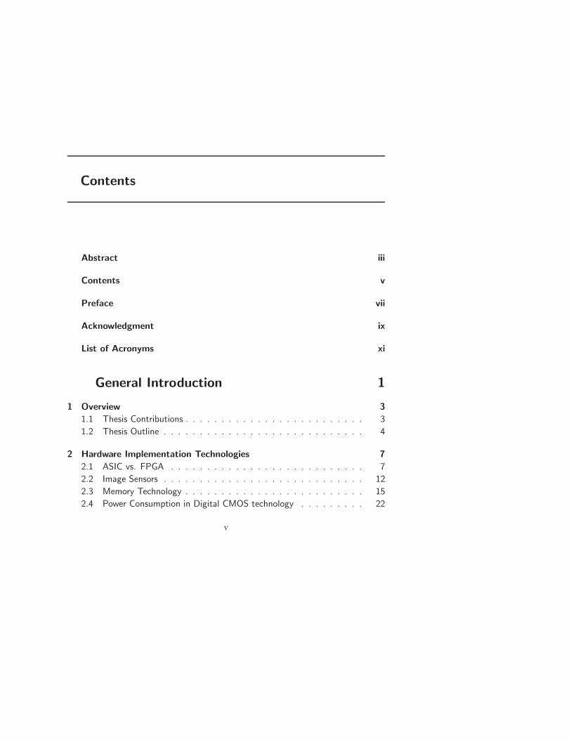
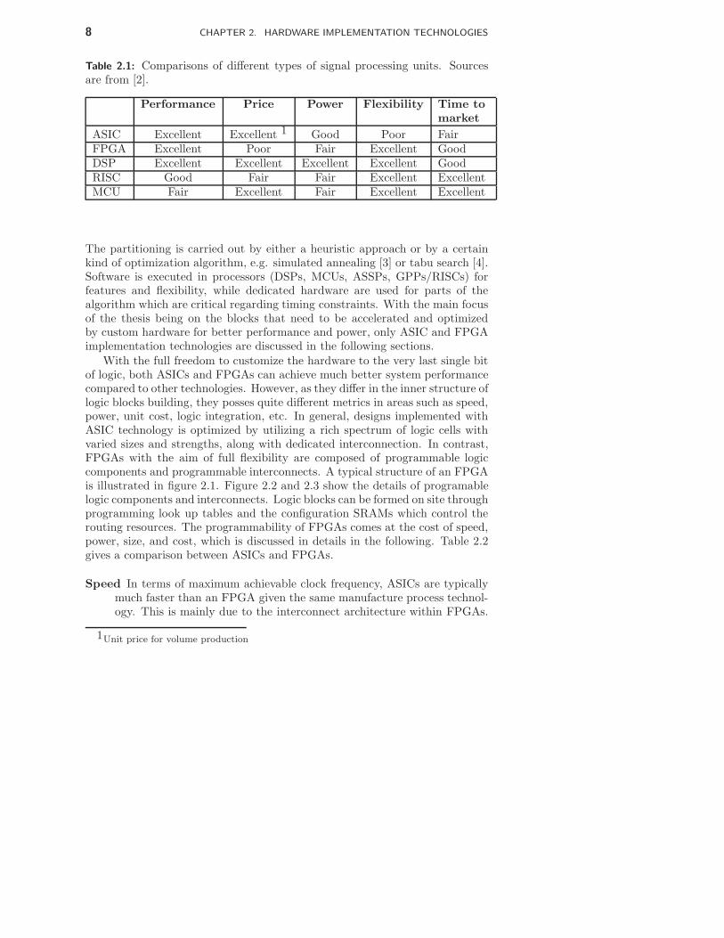
Table 2.1: Comparisons of different types of signal processing units. Sourcesare from [2].
Performance Price Power Flexibility Time to
market
ASIC Excellent Excellent 1 Good Poor FairFPGA Excellent Poor Fair Excellent GoodDSP Excellent Excellent Excellent Excellent GoodRISC Good Fair Fair Excellent ExcellentMCU Fair Excellent Fair Excellent Excellent
The partitioning is carried out by either a heuristic approach or by a certainkind of optimization algorithm, e.g. simulated annealing [3] or tabu search [4].Software is executed in processors (DSPs, MCUs, ASSPs, GPPs/RISCs) forfeatures and flexibility, while dedicated hardware are used for parts of thealgorithm which are critical regarding timing constraints. With the main focusof the thesis being on the blocks that need to be accelerated and optimizedby custom hardware for better performance and power, only ASIC and FPGAimplementation technologies are discussed in the following sections.
With the full freedom to customize the hardware to the very last single bitof logic, both ASICs and FPGAs can achieve much better system performancecompared to other technologies. However, as they differ in the inner structure oflogic blocks building, they posses quite different metrics in areas such as speed,power, unit cost, logic integration, etc. In general, designs implemented withASIC technology is optimized by utilizing a rich spectrum of logic cells withvaried sizes and strengths, along with dedicated interconnection. In contrast,FPGAs with the aim of full flexibility are composed of programmable logiccomponents and programmable interconnects. A typical structure of an FPGAis illustrated in figure 2.1. Figure 2.2 and 2.3 show the details of programablelogic components and interconnects. Logic blocks can be formed on site throughprogramming look up tables and the configuration SRAMs which control therouting resources. The programmability of FPGAs comes at the cost of speed,power, size, and cost, which is discussed in details in the following. Table 2.2gives a comparison between ASICs and FPGAs.
Speed In terms of maximum achievable clock frequency, ASICs are typicallymuch faster than an FPGA given the same manufacture process technol-ogy. This is mainly due to the interconnect architecture within FPGAs.
1Unit price for volume production

2.1. ASIC VS. FPGA 9
Logic block
Configurable routing
I/O block
Figure 2.1: A conceptual FPGA structure with configurable logic blocksand routing.
4 input
Look-up
Table
Inputs
Clock
Mux
D Q
Figure 2.2: Simplified programmable logic elements in an typical FPGAarchitecture.

10 CHAPTER 2. HARDWARE IMPLEMENTATION TECHNOLOGIES
CLB CLB
CLBCLB
MUX
SRAM
SRAM
SRAM
Figure 2.3: Configurable routing resources controlled by SRAMs.
Table 2.2: Comparisons between ASICs and FPGAs.
ASICs FPGAs
Clock speed High LowPower Low High
Unit cost with volume production Low HighLogic Integration High Low
Flexibility Low HighBack-end Design Effort High Low
Integrated Features Low High
2.1. ASIC VS. FPGA 11
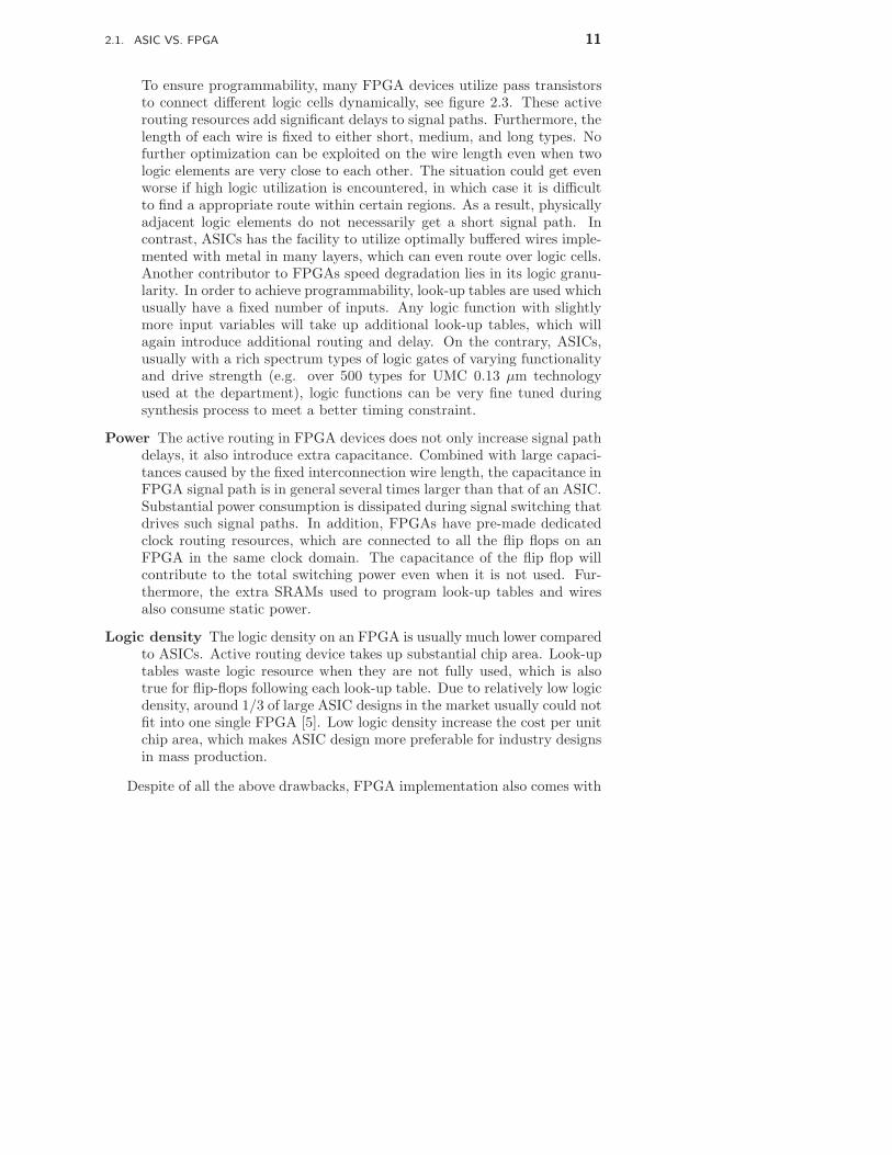
To ensure programmability, many FPGA devices utilize pass transistorsto connect different logic cells dynamically, see figure 2.3. These activerouting resources add significant delays to signal paths. Furthermore, thelength of each wire is fixed to either short, medium, and long types. Nofurther optimization can be exploited on the wire length even when twologic elements are very close to each other. The situation could get evenworse if high logic utilization is encountered, in which case it is difficultto find a appropriate route within certain regions. As a result, physicallyadjacent logic elements do not necessarily get a short signal path. Incontrast, ASICs has the facility to utilize optimally buffered wires imple-mented with metal in many layers, which can even route over logic cells.Another contributor to FPGAs speed degradation lies in its logic granu-larity. In order to achieve programmability, look-up tables are used whichusually have a fixed number of inputs. Any logic function with slightlymore input variables will take up additional look-up tables, which willagain introduce additional routing and delay. On the contrary, ASICs,usually with a rich spectrum types of logic gates of varying functionalityand drive strength (e.g. over 500 types for UMC 0.13 µm technologyused at the department), logic functions can be very fine tuned duringsynthesis process to meet a better timing constraint.
Power The active routing in FPGA devices does not only increase signal pathdelays, it also introduce extra capacitance. Combined with large capaci-tances caused by the fixed interconnection wire length, the capacitance inFPGA signal path is in general several times larger than that of an ASIC.Substantial power consumption is dissipated during signal switching thatdrives such signal paths. In addition, FPGAs have pre-made dedicatedclock routing resources, which are connected to all the flip flops on anFPGA in the same clock domain. The capacitance of the flip flop willcontribute to the total switching power even when it is not used. Fur-thermore, the extra SRAMs used to program look-up tables and wiresalso consume static power.
Logic density The logic density on an FPGA is usually much lower comparedto ASICs. Active routing device takes up substantial chip area. Look-uptables waste logic resource when they are not fully used, which is alsotrue for flip-flops following each look-up table. Due to relatively low logicdensity, around 1/3 of large ASIC designs in the market usually could notfit into one single FPGA [5]. Low logic density increase the cost per unitchip area, which makes ASIC design more preferable for industry designsin mass production.
Despite of all the above drawbacks, FPGA implementation also comes with

12 CHAPTER 2. HARDWARE IMPLEMENTATION TECHNOLOGIES
quite a few advantages, which is served as the motivation in the thesis work.
Verification Ease Due to its flexibility, an FPGA can be re-programmed asrequested when a design flaw is spotted. This is extremely useful forvideo projects, since algorithms for video applications usually need to beverified over a long time period to observe long term effects. Computersimulations are inherently slow. It could take a computer weeks of timeto simulate a video sequences lasting for only several minutes. Besides, anFPGA platform is also highly portable compared to a computer, whichmakes it more feasible to use in heterogeneous environments for systemrobustness verification.
Design Facility Modern FPGAs comes with integrated IP blocks for designease. Most importantly, microprocessors are shipped with certain FP-GAs, e.g. (hard Power PC and soft Microblaze processor cores on VirtexII pro and later version of Xilinx FPGAs). This gives great benefit tohardware/software co-design, which is essential in the presented videosurveillance project. Algorithm such as feature extraction and trackingis more suitable for software implementation. With the facilitation ofvarious FPGA tools, interaction between software and hardware can beverified easily in an FPGA platform. Minor changes in hardware/softwarepartitioning are easier and more viable compared to ASICs.
Minimum Effort Back-end Design The FPGA design flow eliminates thecomplex and time-consuming floor planning, place and route, timing anal-ysis, and mask/re-spin stages of the project, since the design logic is al-ready synthesized to be placed onto an already verified, characterizedFPGA device. This will facilitate hardware designers more time to con-centrate mainly on architecture and logic design task.
From the discussions above, FPGAs are selected as our implementationtechnology due to its fair performance and all the flexibilities and facilities.
2.2 Image Sensors
An image sensor is a device that converts light intensity to an electronic signal.They are widely used among digital cameras and other imaging devices. Thetwo most commonly used sensor technologies are based on Charge Coupled De-vices (CCD) or Complementary Metal Oxide Semiconductor(CMOS) sensors.Descriptions and comparisons of the two technologies are briefly discussed inthe following which are based on [6–8]. A summary of the two sensor typesis given in Table 2.3. Both devices are composed of a array of fundamentallight sensitive elements called photodiodes, which excite electrons (charges)

2.2. IMAGE SENSORS 13
Table 2.3: Image sensor technology comparisons: CCD vs. CMOS.
CCD CMOS
Dynamic Range High ModerateSpeed Moderate High
Windowing Limited ExtensiveCost High Low
Uniformity High Low to moderateSystem Noise Low High
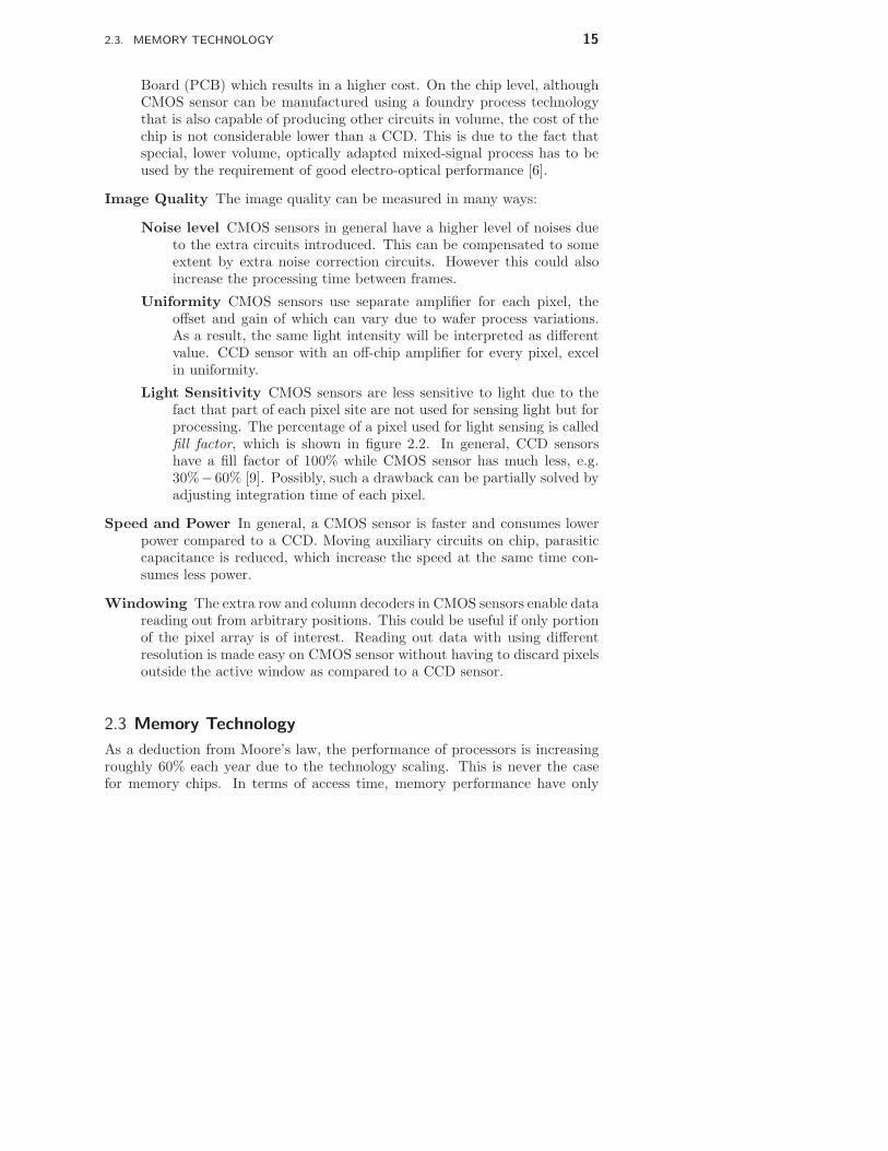
when there is light with enough photons striking on it. In theory, the trans-formation from photon to electron is linear so that one photon would releaseone electron. In general, this is not the case in the real world. Typical imagesensors intended for digital cameras will release less than one electron. Thephotodiode measures the light intensity by accumulating light incident for ashort period of time (integration time), until enough charges are gathered andready to be read out. While CCD and CMOS sensors are quite similar in thesebasic photodiode structure, they mainly differs in the way how these chargesare processed, e.g. readout procedure, signal amplification, and AD conver-sion. The inner structures of the two devices are illustrated in figure 2.4 and2.5. CCD sensors read out charges in a row-wise manner: The charges on eachrow are coupled to the row above, so when the charges are moved down to therow below, new charges from the row above will fill the current position, thusthe name Coupled Charged Device. The CCD shifts one row at a time to thereadout registers, where the charges are shifted out serially through a charge-to-voltage converter. The signal coming out of the chip is a weak analog signal,therefore an extra off-chip amplifier and AD converter are need. In contrast,CMOS sensors integrates separate charge-to-voltage converter, amplifier, noisecorrector and AD converter into each photosite, so the charges are directlytransformed, amplified and digitized to digital signals on each site. Row andcolumn decoders can also be added to select each individual pixel for readoutsince it is manufactured in the same standard CMOS process as main streamlogic and memory devices.
With varied inner structures of the two sensor types, each technology hasunique strengths but also weaknesses in one area or the other, which are de-scribed in the following:
Cost CMOS sensors in general come at a low price at system level since theauxiliary circuits such as oscillator, timing circuits, amplifier, AD con-verter can be integrated onto the sensor chip itself. With CCD sensors,these functionality have to be implemented on a separate Printed Circuit
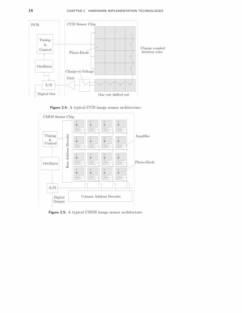
14 CHAPTER 2. HARDWARE IMPLEMENTATION TECHNOLOGIES
PCB
Timing
&
Control
Oscillator
A/D
Digital Out
CCD Sensor Chip
Charge-to-Voltage
Charge coupled
Gain
Photo-Diode between rows
One row shifted out
Figure 2.4: A typical CCD image sensor architecture.
Timing&
Control
Oscillator
A/D
DigitalOutput
CMOS Sensor Chip
Amplifier
Photo-Diode
Column Address Decoder
Row
Addre
ssD
ecoder
Figure 2.5: A typical CMOS image sensor architecture.
2.3. MEMORY TECHNOLOGY 15
Board (PCB) which results in a higher cost. On the chip level, althoughCMOS sensor can be manufactured using a foundry process technologythat is also capable of producing other circuits in volume, the cost of thechip is not considerable lower than a CCD. This is due to the fact thatspecial, lower volume, optically adapted mixed-signal process has to beused by the requirement of good electro-optical performance [6].
Image Quality The image quality can be measured in many ways:
Noise level CMOS sensors in general have a higher level of noises dueto the extra circuits introduced. This can be compensated to someextent by extra noise correction circuits. However this could alsoincrease the processing time between frames.
Uniformity CMOS sensors use separate amplifier for each pixel, theoffset and gain of which can vary due to wafer process variations.As a result, the same light intensity will be interpreted as differentvalue. CCD sensor with an off-chip amplifier for every pixel, excelin uniformity.
Light Sensitivity CMOS sensors are less sensitive to light due to thefact that part of each pixel site are not used for sensing light but forprocessing. The percentage of a pixel used for light sensing is calledfill factor, which is shown in figure 2.2. In general, CCD sensorshave a fill factor of 100% while CMOS sensor has much less, e.g.30%−60% [9]. Possibly, such a drawback can be partially solved byadjusting integration time of each pixel.
Speed and Power In general, a CMOS sensor is faster and consumes lowerpower compared to a CCD. Moving auxiliary circuits on chip, parasiticcapacitance is reduced, which increase the speed at the same time con-sumes less power.
Windowing The extra row and column decoders in CMOS sensors enable datareading out from arbitrary positions. This could be useful if only portionof the pixel array is of interest. Reading out data with using differentresolution is made easy on CMOS sensor without having to discard pixelsoutside the active window as compared to a CCD sensor.
2.3 Memory Technology
As a deduction from Moore’s law, the performance of processors is increasingroughly 60% each year due to the technology scaling. This is never the casefor memory chips. In terms of access time, memory performance have only

16 CHAPTER 2. HARDWARE IMPLEMENTATION TECHNOLOGIES
Light detectionArea
PeripheralCircuits
Figure 2.6: Fill factor refers to the percentage of a photosite that issensitive to light. If circuits cover 25% of each photosite, the sensor issaid to have a fill factor of 75%. The higher the fill factor, the moresensitive the sensor.
managed to increase by less than 10% per year [10, 11]. The performance gapbetween processors and memories has already become a bottle neck of today’shardware system design. With different increase rate, the situation will get evenworse in the future until it reaches a point where further increase in processorspeed yield little or no performance boost for the whole system, a phenomenonthat is called ”hitting the memory wall” from the most cited article [12] by W.Wulf et al. on processor memory gap. The traditional way of bridging the gapis by introducing a hierarchical level of caches, while many new approaches areunder investigation e.g. [13–15]. In order for better understanding of memoryissues today, topics regarding memory technology are given in the followingsection.
In general, memory technology can be categorized into two types, namelyRead Only Memory (ROM) and Random Access Memory (RAM). Due to itsread only nature, a ROM is generally made up of a hardwired architecturewhere a transistor is placed on a memory cell depending on intended contentof the cell. The use of a ROM is limited to store fixed information, e.g. look-up table, micro-codes. Many variant technology exists to provide at least onetime programmability, e.g. PROM, EPROM, EEPROM and FLASH. RAMs onthe other hand with both read and write access are widely used in hardware.Basically, RAMs consists of two types: Static RAM (SRAM) and DynamicRAM (DRAM). A typical 6 transistor SRAM cell is shown in figure 2.7, whilea 1 transistor and a 3 transistor DRAM cells are shown in figure 2.8.

2.3. MEMORY TECHNOLOGY 17
WL
BLBL
VDD
Figure 2.7: An SRAM cell architecture with 6 transistors.
WWL
RWL
BL1 BL2
CS
(a) A 3 transistor DRAM cell structure
CS
BL
WL
CBL
(b) A 1 transistor DRAM cell struc-ture
Figure 2.8: DRAM cell architectures with 1 or 3 transistors.

18 CHAPTER 2. HARDWARE IMPLEMENTATION TECHNOLOGIES
From the figure, static RAM holds its data in a positive feedback loopwith two cascaded inverters. The value will be stored for as long as power issupplied to the circuit. This is in contrast to DRAM, which holds its value on acapacitor. Due to the leakage, the charge on the capacitor will disappear aftera period of time. To be able keep the value, the capacitor has to be refreshedconstantly. With their respective strengths and weaknesses incurred by theirinner structures, SRAMs and DRAMs are used in quite different applications.A brief comparison is made on the two technologies in the following:
Density Each DRAM cell is made up of fewer transistors compared to a SRAMcell, which makes it possible to integrate much more memory cells giventhe same chip area. Due to the same reason, the cost of DRAMs is muchlower.
Speed In general, DRAMs are relatively slow compared to SRAMs. One rea-son for this is that its high density structure leads to large cell arrays withhigh word and bit line capacitance. Another reason lies on its compli-cated read and write cycle with latencies. With its capacity, the addresssignals are multiplexed into row and column due to limited number ofpins, potentially degrading performance. Furthermore, DRAMs needs tobe refreshed constantly, during which period no read and write accessesare possible.
Special IC process Integrating denser cells requires modifications in the man-ufacturing process [16], which makes DRAMs difficult to integrate withstandard logic circuits. In general, DRAMs are manufactured in separatechips.
From these properties, DRAMs are generally used as system memory placedoff-chip due to its density and cost, while SRAMs is placed on-chip with stan-dard logic circuits, working as L1 and L2 caches due to its speed and ease ofintegration.
2.3.1 Synchronous DRAM
To overcome the shortcomings existing in traditional DRAMs, new technologieshave evolved over years, e.g. Fast Page Mode DRAM (FPM), Extended DataOut DRAM (EDO) and Synchronous DRAM (SDRAM). A good overview canbe found from many sources, e.g. [17, 18]. SDRAM gains its popularity byseveral reasons:
• By introducing clock signals, memory buses are made synchronous toprocessors. As a result, the commands to be issued to the memoriesare put in pipelines, so that new operation is executed without waiting

2.3. MEMORY TECHNOLOGY 19
for the completion of the previous ones. Besides, the effort of memorycontroller design is made easier to some extent, since timing parametersare measured in clock cycles instead of physical timing data.
• SDRAM supports burst memory access to an entire row of data. Syn-chronous to the bus clock, the data can be read out sequentially withoutstalling. No column access signals are needed for burst read, the lengthof the burst accessed in set by a mode register, which is a new featurein SDRAMs. Burst data access will increase memory bandwidth sub-stantially if the data needed by the processor are stored successively in arow.
• SDRAM utilize bank interleaving to minimize extra time introduced bye.g. precharge, refresh. The memory space of a SDRAM is divided intoseveral banks (usually two or four). When one of the bank is beingaccessed, other banks remains ready to be accessed. When there is arequest to access another bank, this will take place immediately withouthaving to wait for the current bank to complete. A continuous data flowcan be obtained in such cases.
2.3.1.1 Double Data Rate Synchronous DRAM
To further improve the bandwidth of a SDRAM, Double Data Rate SDRAM(DDR) is developed with doubled memory bandwidth. By using 2n pre-fetchingtechniques, two bits are picked up from the memory array simultaneously tothe I/O buffer in two separate pipelines, where they are to be sent on to the bussequentially on both rising and falling edges of the clock. However, the usage islimited to the situation where the need of multiple accesses is on the same row.In addition to double data rate, the bus signaling technology is changed to a2.5v Stub Series Terminated Logic 2 (SSTL 2) standard [19], which consumesless power. Data strobes signals are also introduced for better synchronizationof data signals to memory controllers.
2.3.2 DDR Controller Design on Xilinx VirtexII pro FPGA
With high data bandwidth and complicated timing parameters of a DDRSDRAM, the design of a DDR interface can be challenging. DDR SDRAMworks synchronously on a clock frequency at 100 MHz or above. Clock sig-nals together with data and command signals are transferred between memoryand processor chips through PCB signal traces. To make sure all data andcommand signals to be valid in the right timing in respective to the clock is anontrivial task. Many factors contributes to the total signal uncertainties, e.g.
20 CHAPTER 2. HARDWARE IMPLEMENTATION TECHNOLOGIES
DC
M
DC
M
Inte
rnal
Exte
rnal
CL
KIN
CL
KIN
CL
KF
B
CL
KF
B
BU
FG
BU
FG
BU
FG
BU
FG
BU
FG
Exte
rnalF
eedba
ckP
CB
Tra
ce
IB
UF
IB
UF
G
OB
UF
OB
UF
IO
BU
FT
R/W
SS
TL
2II
SS
TL
2II
SS
TL
2II
SS
TL
2II
SS
TL
2II
CL
K0
CL
K0
CL
K180
CL
K90
CL
K270
D0
D0
D1
D1
C0
C0
C1
C1
DD
00 11
Ris
eData
FallD
ata
FD
DR
FD
DR
CL
K
DQ
CL
K
DD
R
SD
RA
M
FP
GA
Figure 2.9: Two DCMs are used to synchronize operations on an off-chipDDR SDRAM and on-chip memory controller. DCM external sends off-chip clocks for DDR SDRAM, while DCM internal are used for sendingdata off-chip or capturing data from an DDR SDRAM.
2.3. MEMORY TECHNOLOGY 21
PCB layout skew, package skew, clock phase offset, clock tree skew and clockduty cycle distortion.
In the following, the timing closure of a DDR controller design for the im-plementation of the video surveillance unit is described. The memory interfaceis implemented on a Xilinx Virtex II pro VP30 platform FPGA platform witha working frequency of 100 Mhz.
According to the standard, the data are transferred between a DDR and aprocessor (FPGA in our implementation) with a bidirectional data strobe signal(DQS). The signal is issued by the memory controller during write operationand it is center aligned with the data. During a read operation, the DDR sendthe signal together with the data with edge alignment in respect to each other.
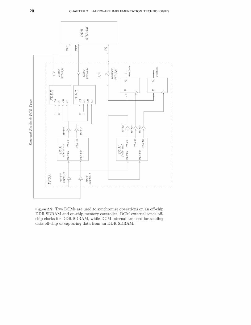
To synchronize the operations between an FPGA and a DDR SDRAM, twoDigital Clock Managers (DCM) are used, which is shown in figure 2.9.
DCM is a special device in many Xilinx FPGA platforms that providemany functionalities related to the clock management, e.g. delayed locked loop(DLL), digital frequency synthesizer and digital phase shifter. By using theclock signal feedback from the dedicated clock tree, the clock signal referencedinternally by each flip-flop inside an FPGA are in phase with the source ofthe clock from off-chip. From figure 2.9, the DCM External generates theclock signals (clk0 and clk180) that go off-chip to the DDR SDRAM throughdouble data rate flip-flops (FDDR). FDDR updates its outputs on the risingedges of both input clock signals. Thus the clock signals to a DDR can bedriven by an FDDR instead of an internal clock signal directly. The DCMInternal generates the clock signals that are used internally by all flip-flops inthe memory controller. To be able to align the two clock signals, they areboth aligned to the original clock source (the signal driven by IBUFG). Thealignment of the DCM External are implemented using a off-chip PCB tracesignals that is designed to have the same length as the clock signal trace fromthe FPGA to the DDR SDRAM. Thus the clock signal arrives at the DDRSDRAM is assumed to be in phase with the external feedback signal thatarrives at the DCM External. As the internal clock signals referenced by allflip-flops in the memory controller are also aligned to the original clock signaldriven by IBUFG through an internal feedback loop, the clock signal in memorycontroller is aligned to the clock signal that arrives at the DDR SDRAM clockpin. During read operation, data are transferred from an off-chip DDR on bothedges of the clock, in a edge alignment manner. To register the data in thememory controller, a 90◦ and 270◦ phase shifted clock signals are used to alignwith the read being data in the center. This is shown in figure 2.9.
In practice, the internal and external clock signals are not entirely in phasewith each other due to skews from many sources. From Xilinx datasheet [20–22], the worst case skews on an Xilinx Virtex II pro devices can result inleading and trailing uncertainties of 880 ps and 540 ps respectively in a read

22 CHAPTER 2. HARDWARE IMPLEMENTATION TECHNOLOGIES
Leading Edge Trailing edgeUncertainty Uncertainty
Delayed CLK90
Read Data
Data Valid Window
880 ps 540 ps830 ps
Leading Edge MarginTrailing Edge Margin
Figure 2.10: DDR read capture data valid window.
data window, which is shown in figure 2.10.The internal DCM is phase shifted by 1 ns to take the advantage of varied
leading and trailing uncertainties, thus the margin of the valid data window isimproved, see figure 2.10.
On the other hand, the timing problem with data write operation is minorsince clock signals and data signals generated within FPGA propagate throughsimilar logics and trace delays.
2.4 Power Consumption in Digital CMOS technology
Minimization of power consumption has been one of the major concerns in thedesign of embedded systems due to one of the following two distinctive reasons:
• The increasing system complexity of portable devices leads to more powerconsumption by more integrated functionality and sophistication, e.g. themultimedia applications on mobile phones such as digital video broadcast-ing (DVB) and digital camera, higher data rate wireless communicationwith emerging technologies such as WiMax/802.16. This shortens batterylife significantly.
• Reliability and cost issues regarding heat dissipation in the manufacturingof non-portable high end applications. High power consumption requires

2.4. POWER CONSUMPTION IN DIGITAL CMOS TECHNOLOGY 23
expensive packaging and cooling techniques given that insufficient coolingleads to high operating temperatures, which tend to exacerbate severalsilicon failure mechanisms.
This is especially true for battery-driven system design. With only 30% batterycapacity increase in the last 30 years and 30 to 40% over the next 5 years byusing new battery technologies [23], e.g.the rechargeable lithium or polymers,the computational power of digital integrated circuits has increased by severalorders of magnitude. To bridge the gap, new approaches must be developed tohandle power consumption in mobile applications.
2.4.1 Sources of power dissipation
Three major sources contribute to the total power dissipation of digital CMOScircuits, which can be formulated as:
Ptot = Pdyn + Pdp + Pstat, (2.1)
where Pdyn is the dynamic dissipation due to charging and discharging load ca-pacitances, Pdp is the power consumption caused by direct path between VDD
and GND with finite slope of the input signal, and Pstat is the static powercaused by leakage current. Traditionally, the power consumption by capacitiveload has always been the dominant factor. This will not be the case in thedesign with deep sub-micron technologies, since leakage current increases ex-ponentially with threshold scaling in each new technology generation [24]. For130 nm technology, leakage can account for 10% to 30% of the total power whenactive, and dominant when standby [25]. With 90 nm and 65 nm technology,the leakage can reach more than 50%. Power dissipation due to direct path,on the other hand, is usually of minor importance, and can be minimized bycertain techniques e.g. supply voltage scaling [26]. With the focus of the the-sis being on architecture exploration, power consumption regarding switchingpower is briefly discussed in the following.
2.4.1.1 Switching Power Reduction Schemes
Power consumption due to signal switching activity can be calculated as [16]:
Pswitch = P0→1CLV 2DDf, (2.2)
where P0→1 is the probability that a output transition of 0 → 1 occurs, CL isthe load capacitance of the driving cell, VDD is the supply voltage, and f is theworking clock frequency. From the equation, power minimization strategy canbe carried out by constraining any of the factors, which is especially effectivefor power supply reduction since the power dissipation decreases quadratically

24 CHAPTER 2. HARDWARE IMPLEMENTATION TECHNOLOGIES
Table 2.4: Power Savings in Different Level of Design Abstraction.
Technique Savings
Architectural/Logic Changes 45%Clock Gating 8%
Low power Synthesis 15%Voltage Reduction 32%
Table 2.5: Core power consumption contribution from different parts of a logiccore [36].
Component Percentage
PLLs/Macros 7.21%Clocks 52.13%
Standard Cells 6.72%Interconnect 5.97%
RAMs (including leakage) 16.94%Logic Leakage 11.04%
with VDD. Power minimization techniques can be applied in all level of designabstractions, ranging from software down to chip layout. In [27–34], compre-hensive overviews of various power reduction techniques are given. Suggestionsare made to minimize power consumption in all level of a circuit design. In [35],a survey is made to give an overview of amount of power savings that can begenerally achieved at different design level. Their experimental results are givenin Table 2.4. From the table, it is shown that the most efficient way of lower-ing power consumption is to work on either high architecture level or the lowtransistor level. In [36], the contributions to the total power consumption fromdifferent blocks of a design are given, which is shown in table2.5. From thetable, it can be seen that clock net and memory access contribute over 50% ofthe total power consumption in the logic core. In the following section, examplepower reduction schemes are discussed, which only covers power consumptionminimization in high level architecture design.
2.4.2 Pipelining and Parallel Architectures
Power consumption can be reduced by using pipelining or parallel architectures.According to [37], the first order estimation of the delay of a logic path can be

2.4. POWER CONSUMPTION IN DIGITAL CMOS TECHNOLOGY 25
calculated as
td ∝ VDD
(VDD − Vt)α. (2.3)
With a pipelining architecture, the calculation paths of a design is inserted withpipeline registers. This effectively reduces the td in the critical path. ThusVDD can be lowered in the equation while the same clock frequency can bemaintained. As stated above, power consumption can be reduced by loweringVDD since it has quadratic effects on power dissipation. The same principleapplies to parallel architecture. With hardware duplicated several times, thethroughput of a design increases proportionally. Alternatively, a design canachieve for lower power consumption by slowing down the clock frequency ofeach duplicates. The same throughput is maintained, while the supply voltagecan be reduced.

Bibliography
[1] C. Stauffer and W. Grimson, “Adaptive background mixture models forreal-time tracking,” in Proc. IEEE Conference on Computer Vision andPattern Recognition, 1999.
[2] L. Adams. (2002, November) Choosing the right architec-ture for real-time signal processing designs. [Online]. Available:http://focus.ti.com/lit/an/spra879/spra879.pdf
[3] P. Eles, Z. Peng, K. Kuchcinski, and A. Doboli, “System level hard-ware/software partitioning based on simulated annealing and tabu search,”Springer Design Automation for Embedded Systems, vol. 2, pp. 5–32, Jan-uary 1997.
[4] T. Wiangtong, P. Y. Cheung, and W. Luk, “Tabu search with intensifica-tion strategy for functional partitioning in hardware-software codesign,”in Proc. of the 10 th Annual IEEE Symposium on Field-ProgrammableCustom Computing Machines (FCCM 02), California, USA, April 2002,pp. 297– 298.
[5] J. Gallagher. (2006, January) ASIC prototyping using off-the-shelf FPGA boards: How to save months of verificationtime and tens of thousands of dollars. [Online]. Available:http://www.synplicity.com/literature/whitepapers/pdf/proto wp06.pdf
[6] D. Litwiller. (2001, January) CCD vs. CMOS: Facts and fic-tion. [Online]. Available: http://www.dalsa.com/shared/content/Photonics Spectra CCDvsCMOS Litwiller.pdf
27

28 BIBLIOGRAPHY
[7] ——. (2005, August) CMOS vs. CCD: Maturing technologies, maturingmarkets. [Online]. Available: http://www.dalsa.com/shared/content/pdfs/CCD vs CMOS Litwiller 2005.pdf
[8] A. E. Gamal and H. Eltoukhy, “CMOS image sensors,” IEEE Circuits andDevice Magzine, vol. 21, pp. 6–20, May-June 2005.
[9] D. Scansen. CMOS challenges CCD for image-sensinglead. [Online]. Available: http://www.eetindia.com/articles/2005oct/b/2005oct17 stech opt ta.pdf
[10] J. L. Hennessy and D. A. Patterson, Computer Architecture: A Quantita-tive Approach, Third Edition. Morgan Kaufmann, 2002.
[11] N. R. Mahapatra and B. Venkatrao, “The processor-memory bot-tleneck: Problems and solutions,” Tech. Rep. [Online]. Available:http://www.acm.org/crossroads/xrds5-3/pmgap.html
[12] W. A. Wulf and S. A. McKee, “Hitting the memory wall: Implicationsof the obvious,” Computer Architecture News, vol. 23, pp. 20–24, March1995.
[13] “The berkeley intelligent RAM (IRAM) project,” Tech. Rep. [Online].Available: http://iram.cs.berkeley.edu/
[14] C. C. Liu, I. Ganusov, M. Burtscher, and S. Tiwari, “Bridging the proces-sor memory performance gap with 3D IC technology,” IEEE Design andTest of Computers, vol. 22, pp. 556– 564, November 2005.
[15] “puma2, proactively uniform memory access architecture,” Tech. Rep.[Online]. Available: http://www.ece.cmu.edu/ puma2/
[16] J. M. Rabaey, A. Chandrakasan, and B. Nikolic, Digital Integrated Cir-cuits: A Design Perspective, Second Edition. Prentice Hall, 2003.
[17] T.-G. Hwang, “Semiconductor memories for it era,” in Proc. of IEEEInternational Solid-State Circuits Conference (ISSCC), California, USA,February 2002, pp. 24–27.
[18] (2005) Memory technology evolution. [On-line]. Available: http://h20000.www2.hp.com/bc/docs/support/SupportManual/c00266863/c00266863.pdf
[19] [Online]. Available: http://download.micron.com/pdf/misc/sstl 2spec.pdf

BIBLIOGRAPHY 29
[20] M. George. (2006, December) Memory interface applicationnotes overview. [Online]. Available: http://www.xilinx.com/bvdocs/appnotes/xapp802.pdf
[21] N. Gupta and M. George. (2004, May) Creating high-speed memoryinterfaces with Virtex-II and Virtex-II Pro FPGAs. [Online]. Available:http://www.xilinx.com/bvdocs/appnotes/xapp688.pdf
[22] N. Gupta. (2005, January) Interfacing Virtex-II de-vices with DDR SDRAM memories for performance to167 mhz. [Online]. Available: http://www.xilinx.com/support/software/memory/protected/XAPP758c.pdf
[23] W. L. Goh, S. S. Rofail, and K.-S. Yeo.Low-power design: An overview. [Online]. Available:http://www.informit.com/articles/article.asp?p=27212&rl=1
[24] G. E. Moore, “No exponential is forever: But ”Forever” can be delayed!”in Proc. of IEEE International Solid-State Circuits Conference (ISSCC),California, USA, February 2003, pp. 20–23.
[25] B. Chatterjee, M. Sachdev, S. Hsu, R. Krishnamurthy, and S. Borkai,“Effectiveness and scaling trends of leakage control techniques for sub430nm CMOS technologies,” in Proc. of International Symposium on LowPower Electronics and Design (ISLPED), California, USA, August 2003,pp. 122–127.
[26] T. Olsson, “Distributed clocking and clock generation in digital CMOSSoC ASICs,” Ph.D. dissertation, Lund University, Lund, 2004.
[27] J. M. Rabaey and M. Pedram, Low Power Design Methodologies.Springer, 1995.
[28] A. P. Chandrakasan, S. Sheng, and R. W. Brodersen, “Low-power CMOSdigital design,” IEEE Journal of Solid-State Circuits, vol. 27, pp. 473 –484, April 1992.
[29] D. Garrett, M. Stan, and A. Dean, “Challenges in clockgating for a lowpower ASIC methodology,” in Proc. of International Symposium on LowPower Electronics and Design, California, USA, August 1999, pp. 176 –181.
[30] Y. J. Yeh, S. Y. Kuo, and J. Y. Jou, “Converter-free multiple-voltage scal-ing techniques for low-power CMOS digital design,” IEEE Transactionson Computer-Aided Design of Integrated Circuits and Systems, vol. 20, pp.172 – 176, January 2001.
30 BIBLIOGRAPHY
[31] T. Kuroda and M. Hamada, “Low-power CMOS digital design with dualembedded adaptive power supplies,” IEEE Journal of Solid-State Circuits,vol. 35, pp. 652 – 655, April 2000.
[32] A. Garcia, W. Burleson, and J. L. Danger, “Low power digital design inFPGAs: a study of pipeline architectures implemented in a FPGA using alow supply voltage to reduce power consumption,” in Proc. IEEE Interna-tional Symposium on Circuits and Systems (ISCAS), Geneva, Switzerland,May 2000, pp. 561 – 564.
[33] P. Brennan, A. Dean, S. Kenyon, and S. Ventrone, “Low power method-ology and design techniques for processor design,” in Proc. InternationalSymposium on Low Power Electronics and Design (ISLPED), California,USA, August 1998, pp. 268 – 273.
[34] L. Benini, G. D. Micheli, and E. Macii, “Designing low-power circuits:practical recipes,” IEEE Circuits and Systems Magazine, vol. 1, pp. 6–25,2001.
[35] F. G. Wolff, M. J. Knieser, D. J. Weyer, and C. A. Papachristou, “High-level low power FPGA design methodology,” in Proc. IEEE Conference onNational Aerospace and Electronics Conference (NAECON), Ohio, USA,October 2000, pp. 554–559.
[36] S. GadelRab, D. Bond, and D. Reynolds, “Fight the power: Power re-duction ideas for ASIC designers and tool providers,” in Proc. of SNUGConference, California, USA, 2005.
[37] K. K. Parhi, VLSI Digital Signal Processing Systems: Design and Imple-mentation. John Wiley & Sons, 1999.

Hardware Accelerator
Design of an Automated
Video Surveillance
System
31


Chapter 1
Segmentation
1.1 Introduction
The use of video surveillance systems is omnipresent in the modern world inboth a civilian and a military contexts, e.g. traffic control, security monitor-ing and antiterrorism. While traditional Closed Circuit TV (CCTV) basedsurveillance systems put heavy demands of human operators, there is an in-creasing needs for automated video surveillance system. By building a selfcontained video surveillance system capable of automatic information extrac-tion and processing, various events can be detected automatically, and alarmscan be triggered in presence of abnormity. Thereby, the volume of data pre-sented to security personnel is reduced substantially. Besides, automated videosurveillance better handles complex cluttered or camouflaged scenes. A videofeed for surveillance personnel to monitor after the system has announced anevent will support improved vigilance and increase the probability of incidentdetection.
Crucial to most of such automated video surveillance systems is the qualityof the video segmentation, which is a process of extracting objects of interest(foreground) from an irrelevant background scene. The foreground information,often composed of moving objects, is passed on to later analysis units, where ob-jects are tracked and their activities are analyzed. To be able to perform videosegmentation, a so called background subtraction technique is usually applied.With a reference frame containing a pure background scene being maintainedfor all pixel locations, foreground objects are extracted by thresholding thedifference between the current video frame and the background frame. In the
33
34 CHAPTER 1. SEGMENTATION
50 100 150 200 250 300
50
100
150
200
(a) Indoor environment in the lab
50 100 150 200 250 300
50
100
150
200
(b) TH = 5
50 100 150 200 250 300
50
100
150
200
(c) TH = 10
50 100 150 200 250 300
50
100
150
200
(d) TH = 20
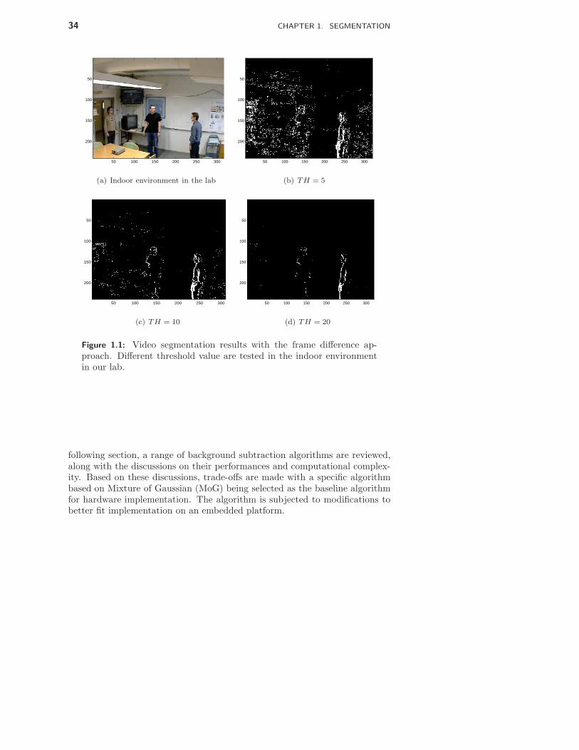
Figure 1.1: Video segmentation results with the frame difference ap-proach. Different threshold value are tested in the indoor environmentin our lab.
following section, a range of background subtraction algorithms are reviewed,along with the discussions on their performances and computational complex-ity. Based on these discussions, trade-offs are made with a specific algorithmbased on Mixture of Gaussian (MoG) being selected as the baseline algorithmfor hardware implementation. The algorithm is subjected to modifications tobetter fit implementation on an embedded platform.

1.2. ALTERNATIVE VIDEO SEGMENTATION ALGORITHMS 35
1.2 Alternative Video Segmentation Algorithms
1.2.1 Frame Difference
A Background/Foreground detection can be achieved by simply observing thedifference of the pixels between two adjacent frames. By setting a thresholdvalue, a pixel is identified as foreground if the difference is higher than thethreshold value or background otherwise. The simplicity of the algorithm comesat the cost of the segmentation quality. In general, bigger regions are detectedas foreground area than the actual moving part. Also it fails to detect innerpixels of a large, uniformly-colored moving object, a problem known as apertureeffect [1]. In addition, setting a global threshold value is problematic since thesegmentation is sensitive to light intensity. Figure 1.1 shows segmentationresults with a video sequence taken in our lab, where three people are movingin front of a camera. From these figures, it can be seen that with lower thresholdvalue, more details of the moving objects are revealed. However, this comeswith substantial noise that could overwhelm the segmented objects, e.g. the leftmost person in figure 1.1(b). On the other hand, increasing the threshold valuereduces noise level, at the cost of less details detected to a point where almostwhole objects are missing, e.g. left most person in figure 1.1(d). In general,inner parts of all objects are left undetected, due to their uniformity colors thatresult in minor value changes over frames. In spite of the segmentation quality,the frame difference approach suits well for hardware implementation. Thecomputational complexity as well as memory requirements are rather low. Withthe memory size of only one video frame and minor hardware calculation, e.g.an adder and a comparator, it is still found as part of many video surveillancesystems of today [1–4].
1.2.2 Median Filter
While the frame difference approach uses the previous frame as the backgroundreference frame, it is inherently unreliable and sensitive to noise with the mov-ing objects contained in the reference frame and the varying illumination noiseover frames. An alternative approach to obtain a background frame is by usingmedian filters. A median filter has traditionally been used in spatial image fil-tering process to remove noise [5]. The basic idea of noise reduction lies in thefact that a pixel corrupted by noise makes a sharp transition in the spatial do-main. By checking the surrounding pixels that centers at the pixel in question,the middle value is selected to replace the center pixel. By doing this, the pixelin question is forced to look like its neighbors, thus the extinctive pixel valuecorrupted by noise are replaced. Inspired by this, median filters are used tomodel background pixels with reduced noise deviation by filtering pixel values

36 CHAPTER 1. SEGMENTATION
in the time domain. they are used in many applications [6–8], with the medianfiltering process carried out over the previous n frames, e.g. 50 − 200 framesin [6]. To avoid foreground pixel values to be mixed into the background, thenumber of frames has to be large so that more than half the pixel values be-longs to the background. The principle is illustrated in figure 1.2, where thenumber of both foreground and background pixels are shown in a frame buffer.Due to various noise, a pixel value will not stay at exactly the same value overframes, thus the histograms are used to represent both the foreground and thebackground pixels. Consider the case when the number of background pixelsis more than that of foreground pixel by only one. The median value will lieright at the right foot of background histogram. With increasing backgroundpixel filled into the buffer, the value is moving towards the peak of the back-ground histogram. Under the previous assumption that no foreground pixelwill stay in the scene for more than half size of the buffer, the median valuewill move along the background histogram back and forth, representing thebackground pixel value for the current frame. Using buffers to store previousn frames is costly in memory usage. In certain situations, number of bufferedframes could increase substantially, e.g. slowly moving objects with uniformlycolored surface are present in the scene or the foreground objects stopped for awhile before moving on to another location. The calculation complexity is alsoproportional to the number of buffers. To find the median value it is necessaryto sort all the values in the frame buffer in numerical order which is hardwarecostly with large number of frame buffers.
1.2.3 Selective Running Average
One similar alternative to median filtering is to use the average instead of themedian value over previous n frames. Noise distortions to a background pixelover frames can be neutralized by taking the mean value of the pixel samplescollected over time. To avoid huge memory requirements similar to the medianfiltering approach, a running average can be utilized which takes the form of
Bt = (1 − α)Bt−1 + αFt, (1.1)
where α is the learning rate, F and B are the current frame and backgroundframe formed by the mean value of each pixel respectively. With such anapproach, only a frame of mean values are needed to be stored in a memory.The average operation is carried out by incorporating a small portion of thenew frames into the mean values at a time, using a learning factor α. At thesame time, the same portion of the current mean value is discarded. Dependingon the value of α, such a average operation can be fast or slow. For backgroundmodeling, a fast learning factor could result in foreground pixels to be quicklyincorporated into background, thus limiting its usage to certain situations, e.g.

1.2. ALTERNATIVE VIDEO SEGMENTATION ALGORITHMS 37
0 20 40 60 80 100 1200
10
20
30
40
50
60
70
Color Intensity level
Num
ber
of p
ixel
backgroundpixels
median value
foregroundpixels
Figure 1.2: Foreground and Background pixel histograms: With morepixels in the buffer falling within Background, the median value movestowards the center of Background distribution.
initialization phase with only background scene.To avoid a foreground pixel to be mixed into the background updating
process, a selective running average can be applied. This is shown in thefollowing equations:
Bt = (1 − α)Bt−1 + αFt if Ft ⊂ background (1.2)
Bt = Bt−1 if Ft ⊂ foreground. (1.3)
With the foreground/background distinction performed before backgroundframe updating process, more recent “clean” background pixels contributes tothe form of the new mean value, which makes the background modeling moreaccurate. The selective running average method is used in many applications,e.g. [9, 10], and forms the basics of other alternative algorithms with muchhigher complexity, e.g. Mixture of Gaussian (MOG) discussed in the follow-ing sections. The merit of the approach comes in its relatively low hardwarecomplexity, e.g. simple multiplications and additions are needed to update themean value for each pixel. Together with low memory requirements of storing

38 CHAPTER 1. SEGMENTATION
only one frame of mean values, running selective average fits well for hardwareimplementation. Acting virtually with the same principles as a mean filter,selective running average achieves similar segmentation results as that of themedian filtering approach.
1.2.4 Linear Predictive Filter
To be able to estimate the current background more accurately, linear predictivefilters are developed for background modeling in several literatures [11–15]. Theproblem with taking the median or mean of the past pixel samples lies in thefact that it does not reflect the uncertainty (variance) of how a backgroundpixel value could drift from its mean value. Without any of this information,the foreground/background distinction has to be done in a heuristic way. Analternative approach can be utilized which predicts the current backgroundpixel value from its recent history values. Compared to mean and medianvalues, a prediction value can more accurately represent the true value of thecurrent background pixel, which effectively decrease the uncertainty of thevariation of a background pixel. As a result, a tighter threshold value canbe selected to achieve a more precise segmentation with a better chance ofavoiding camouflage problem, where foreground and background holds similarpixel values. Toyama et al. [11] uses an one-step Wiener filter to predict abackground value based on its recent history of values. In their approach, alinear estimation of the current background value is calculated as:
Bt =
N∑
k=1
αkIt−k, (1.4)
where B is the current background estimation, It−k is one of the history valuesof a pixel, and αk is the prediction coefficient. The coefficient are calculated tominimize mean square of the estimation error, which is formulated as:
E[e2t ] = E[(Bt − Bt)
2]. (1.5)
According to the procedure described in [16], the coefficients can be obtainedby solving a set of linear equations as follows:
p∑
k=1
αk
∑
t
It−kIt−i = −∑
t
ItIt−i, 1 ≤ i ≤ p. (1.6)
The estimation of coefficients and pixel predictions are calculated recursivelyduring each frame. In [11], a pixel value with a deviation of more than 4.0 ×√
E[e2t ] is considered foreground pixel. In total, 50 past values are used in [11]
for each pixel to calculate 30 coefficients.

1.2. ALTERNATIVE VIDEO SEGMENTATION ALGORITHMS 39
Wiener filters are also expensive in computation and memory requirement.N frame buffers are needed to store a history of frames. Background pixelprediction and coefficients updating are very costly since a set of linear functionsare needed to obtain the value. p multiplication and p−1 additions are neededfor prediction, plus the solution of a linear equation of order p.
An alternative approach for linear prediction is to use Kalman filters. BasicKalman filter theory can be found in many literatures, e.g. [12,13,15]. Kalmanfilters are widely used for many background subtraction applications, e.g. [13–15]. It predicts the current background pixel value by recursive computingfrom the previous estimate and the new input data. A brief formulation of thetheory is given in the below according to [13], while a detailed description ofKalman filters can be found in [12].
Kalman filters provide an optimal estimate of the state of the process xt,by minimizing the difference of the average of the estimated outputs and theaverage of the measures, which is characterized by the variance of the estimationerror. The definition of a state can vary in different applications, e.g. theestimated value of the background pixel and its derivative in [15]. Kalmanfiltering is performed in essentially two steps: prediction and correction: In theprediction step, the current state of the system is predicted from the previousstate as
x−
t = Axt−1, (1.7)
where A is the state transition matrix, xt−1 is the previous state estimate andx−
t is the estimation of the current state before correction. In order to minimizethe difference between the measure and the estimated state value It −Hx
−
t . It
is the current observation and H is the transition matrix that maps the stateto the measurements. A variance of such difference is calculated based on
P−
t = APt−1AT + Qt, (1.8)
where Qt represents the process noise, Pt−1 is the previous estimation errorvariance and P−
t is the estimation of error variance based on current predictionstate value. With a filter gain factor calculated by
Kt =P−
t CT
CP−
t CT + Rt
, (1.9)
where Rt represents the variances of measurement noise and C is the transitionmatrix that maps the state to the measurement. The corrected state estimationbecomes
xt = xt−1 + Kt(It − Hx−
t ), (1.10)
and the variance after correction is reduced to
Pt = (1 − KtC)P−
t . (1.11)

40 CHAPTER 1. SEGMENTATION
Ridder et al. [15] use both background pixel intensity value and its temporalderivative Bt and B′
t as the state value:
xt =
[
Bt
B′
t
]
, (1.12)
and the parameters are selected as follows:
A =
[
1 0.70 0.7
]
and H =[
1 0]
. (1.13)
The gain factor Kt varies between a slow adaptation rate α1 and a fastadaptation rate α2 depending on whether the current observation is a back-ground pixel or not:
Kt =
[
α1
α1
]
if It−1 is foreground, and
[
α2
α2
]
otherwise. (1.14)
In summary, a recursive background prediction approach with Kalman fil-ters can be obtained by combining equations 1.10,1.12,1.13 and 1.14, which canbe formulated as follows:
[
Bt
B′
t
]
= A
[
Bt−1
B′
t−1
]
+ Kt
(
It − HA
[
Bt−1
B′
t−1
])
. (1.15)
The Kalman filtering approach is efficient for hardware implementation.From equation 1.15, three matrix multiplication with size of 2 are needed.Memory requirement is low with one frame of estimated background pixel valuestored. The linear predictive approach is reported to achieve better resultsthan the many other algorithms e.g. median or mean filtering approaches,especially in dealing with camouflage problem [11], where foreground pixelsholding similar color as that of the background pixels are undetected.
1.2.5 Mixture of Gaussian
So far, predictive methods have been discussed which model the backgroundscene as a time series and develop a linear dynamical model to recover the cur-rent input based on past observations. By minimizing the variance between thepredicted value and past observations, the estimated background pixel is adap-tive to the current situation where its value could vary slowly over time. Whilethis class of algorithms may work well with quasi-static background scenes withslow lighting changes, it fails to deal with multi-modal situations, which willbe discussed in detail in the following sections. Instead of utilizing the orderof incoming observations to predict the current background value, a Gaussian
1.2. ALTERNATIVE VIDEO SEGMENTATION ALGORITHMS 41
distribution can be used to model a static background value by accounting forthe noise introduced by small illumination changes, camera jitter and surfacetexture. In [17], three Gaussian are used to model background scenes for trafficsurveillance. The hypothesis is made that each pixel will contain the color ofeither the road, the shadows or the vehicles. Stauffer et al. [18] generalizedthe idea by extending the number of Gaussian for each pixel to deal with amulti-modal background environment, which are quite common in both indoorand outdoor environments. A multi-modal background is caused by repetitivebackground object motion, e.g. swaying trees or flickering of a monitor. As apixel lying in the region where repetitive motion occurs will generally consistsof two or more background colors, the RGB value of that specific pixel will haveseveral pixel distributions in the RGB color space. The idea of multi-modaldistribution is illustrated by figure 1.3. From the figure, a typical indoor envi-ronment in 1.3(a) consists of static background objects, which are stationaryall the time. A pixel value in any location will stay within one single distri-bution over time. This is in contrast with the outdoor environment in figure1.3(c), where quasi-static background objects e.g. swaying leaves of a tree, arepresent in the scene. Pixel value from these regions contains multiple back-ground colors from time to time, e.g. the color of the leave, the color of houseor something in between.
With multi-modal environments, the value of quasi-static background pixelstends to jump between different distributions, which will be modeled by fittingdifferent Gaussians for each distribution. The idea of Mixture of Gaussians(MoG) is quite popular and many different variants are developed [19–24] basedon it.
1.2.5.1 Algorithm Formulation
The Stauffer-Grimson algorithm is formulated as modeling a pixel process witha mixture of Gaussian distributions. A pixel process is defined as the recenthistory values of each pixel obtained from a number of consecutive frames.For a static background pixel process, the values will rather be pixel clustersthan identical points when they are plotted in a RGB color space. This is dueto the variations caused by many factors, e.g. surface texture, illuminationfluctuations, or camera noise. To model such a background pixel process, aGaussian distribution can be used with a mean equal to the average backgroundcolor and variances accounting for the value fluctuation. More complicatedbackground pixel processes appear when it contains more than one backgroundobject surfaces, e.g. a background pixel of a road is covered by leaves of atree from time to time. In such cases, a mixture of Gaussian distributionsare necessary to model multi-modal background distributions. Formally, theStauffer-Grimson algorithm tries to address background modeling as in the

42 CHAPTER 1. SEGMENTATION
50 100 150 200 250 300
50
100
150
200
(a) A typical indoor environment taken inthe staircase.
7080
90100
110
60
70
80
90
30
40
50
60
70
80
90
RG
B
(b) A pixel value sampled over time inthe indoor environment contains uni-modalpixel distributions.
50 100 150 200 250 300
50
100
150
200
(c) A dynamic outdoor environment con-taining swaying trees.
160
180
200
220
190200
210220
230180
190
200
210
220
230
240
RG
B
(d) A pixel value sampled over time in theregion that contain leaves of a tree will gen-erally become multi-modal distributions inthe RGB color space.
Figure 1.3: Background pixel distributions taken in different environ-ments possess different properties in the RGB color space.
following:
Each pixel is represented by a set of Gaussian distributions k ⊂ {1, 2...K},where the number of distributions K is assumed to be constant (usually be-tween 3 and 7). Some of the K distributions correspond to background objectsand the rest are regarded as foreground. Each of the mixture of Gaussians isweighted with a parameter ωk, which represents probability of current obser-vation belonging to the distribution, thus the equation
ΣKk=1ωk = 1. (1.16)
The probability of the current pixel value X being in distribution k is cal-

1.2. ALTERNATIVE VIDEO SEGMENTATION ALGORITHMS 43
0 50 100 150 200 250 3000
0.005
0.01
0.015
0.02
0.025
Color intensity level
Pro
babi
lity
Gauss1
Mixture of Gauss
Gauss2
Gauss3
Figure 1.4: Three Gaussian distributions are plotted in the figure withtheir mean and variance as {80, 20}, {100, 5}, {200, 10} respectively.Their prior weight is specified as {0.2, 0.2, 0.6}. The probability of anew pixel observation belonging to one of the distributions can be seenas a sum of three Gaussian distributions [25].
culated as:
f(X |k) =1
(2π)n2 |Σk|
12
e−12 (X−µk)T Σ−1
k(X−µk), (1.17)
where µk is the mean and Σk is the covariance matrix of the Kth distribution.Thus, the probability of a pixel belonging to one of the Gaussian distribution isthe sum of probabilities of belonging to each of the Gaussian distribution, whichis illustrated in 1.4 [25]. A further assumption is usually made that the differentcolor component is independent of each other so that the covariance matrixis diagonal - more suitable for calculations, e.g. matrix inversion. Staufferet.al. go even further in assuming that the variances are identical, implying forexample that deviations in the red, green, and blue dimensions of a color spacehave the same statistics. While such simplification reduce the computationalcomplexity, it has certain side effects which will be discussed in the followingsections.

44 CHAPTER 1. SEGMENTATION
The most general solution to the foreground segmentation can be brieflyformulated as: at each sample time t, the most likely distribution k from a setof observations is estimated from X, along with a procedure for demarcatingthe foreground states from the background states.
This is done by the following: A match is defined as the incoming pixelwithin J times the standard deviation off the center, where in [18] J is selectedas 2.5. Mathematically, the portion of the Gaussian distributions belonging tothe background is determined by
B = argminb
(
b∑
k=1
ωk > H
)
, (1.18)
where H is a predefined parameter and ωk is the weight of distribution k. If amatch is found, the matched distribution is updated as:
ωk,t = (1 − α)ωk,t−1 + α (1.19)
µt = (1 − ρ)µt−1 + ρXt (1.20)
σ2 = (1 − ρ)σ2t−1 + ρ(Xt − µt)
T (Xt − µt); (1.21)
where µ, σ are the mean and variance respectively, α, ρ are the learning factors,and Xt are the incoming RGB values. The mean, variance and weight factorsare updated frame by frame. For those unmatched, the weight is updatedaccording to
ωk,t = (1 − α)ωk,t−1, (1.22)
while the mean and the variance remain the same. If none of the distributionsare matched, the one with the lowest weight is replaced by a distribution withthe incoming pixel value as its mean, a low weight and a large variance.
1.2.6 Kernel Density Model
In [26], it was discovered that the histogram of a dynamic background in anoutdoor environment covers a wide spectrum of gray levels (or intensity levelof different color component), and all these variations occur in a short periodof time, e.g. 30 seconds. Modeling such a dynamic background scene with alimited number of Gaussian distributions are not feasible.
In order to adapt fast to the very recent information about an image se-quence, a kernel density function background modeling can be used which onlyuse a recent history of past values to distinguish foreground from backgroundpixels.
Given a history of past values x1, x2,...xN , a kernel density function can beformulated as the following:
1.2. ALTERNATIVE VIDEO SEGMENTATION ALGORITHMS 45
The probability of a new observation having a value of xt can be calculatedusing a density function:
Pr(xt) =1
n
N∑
i=1
K(xt − xi). (1.23)
What this equation actually indicates is that a new background observationcan be predicted by the combination of its recent past history samples. If K ischosen to be a Gaussian distribution, then the density estimation becomes
Pr(xt) =1
N
N∑
i=1
1
(2π)d2 |Σ| 12
e−12 (xt−xi)
T Σ−1(xt−xi). (1.24)
Under similar assumptions as the mixture of Gaussian approach, if differentcolor components are independent of each other, the covariance matrix Σ be-comes
Σ =
δ21 0 00 δ2
2 00 0 δ2
3
(1.25)
and the density estimation is reduced to
Pr(xt) =1
N
N∑
i=1
d∏
j=1
1√
2πδ2j
e−
12
(xtj−xij
)2
δ2j . (1.26)
From the definition of probability estimation, a foreground/backgroundclassification process can be carried out by checking the probability valueagainst a threshold value, e.g. if Pr(xt) < th, the new observation can notbe predicted by its past history, thus recognized as a foreground pixel. Kerneldensity estimation generalize the idea of the Gaussian mixture model, whereeach single sample of the N samples is considered to be a Gaussian distribu-tion by itself. Thus it can also handle multi-modal background scenarios. Theprobability calculation only depends on its N past values, which makes thealgorithm quickly adapt to the dynamic background scene.
Regarding hardware implementation complexity, the kernel density modelneeds to store N past frames, which makes it a memory intensive task. Thecalculation of probability in equation 1.26 is costly. In [26], a look-up tableis suggested to store precalculated value for each xt − xi. This will furtherincrease the requirement on the memory.
1.2.7 Summary
A wide range of segmentation algorithms have been discussed, each with re-lated robustness to different situations and each with different computational

46 CHAPTER 1. SEGMENTATION
Table 1.1: Algorithm Comparison.
FD Median LPF MoG KDEAlgorithm per-formance
fast fast medium medium slow
Memory re-quirement
1 frame 50− 300frames
1 frame ofmean
1 frameof kGaus-sianparame-ters
nframesof kGaus-sianparame-ters
Segmentationquality
worst low acceptable good best
Hardwarecomplexity
very low medium low tomedium
low high
complexity. A comparison is made in [11] on segmentation qualities of some ofthe algorithms. In fact, an unbiased comparison with a significant benchmarkis absent. No perfect system exists to handle all kinds of issues within differ-ent background models. Furthermore, for realistic implementation of such asystem, trade-offs have to be made between system robustness (quality) andsystem performance (frame rate, resolution, etc.). From the discussion above,a summary is made in Table 1.1 concerning Algorithm performance, memoryrequirements, the segmentation quality and hardware complexity.
From the table, it can be seen that Stauffer-Grimson algorithm gives goodsegmentation quality with relatively low hardware complexity and memoryrequirements. In [18], a frame rate of 11-13 FPS is obtained for a frame sizeof 160×120 on an SGI O2 workstation. In our software implementation on anAMD 4400+ processor, a frame rate of 4-6 FPS is observed for video sequenceswith 352×288 resolution.
In this thesis, the hardware accelerator design is based on Stauffer-Grimsonalgorithm with several modifications for better segmentation quality and hard-ware efficiency. A variety of memory access reduction schemes are implemented,resulting in more than 70% memory bandwidth reduction.
1.3 Algorithm Modifications
The Mixture of Gaussian algorithm works efficiently only in controlled envi-ronments. Issues regarding algorithm weaknesses in different situations areaddressed in many publications [19–21, 23]. In this section, instead of mainly
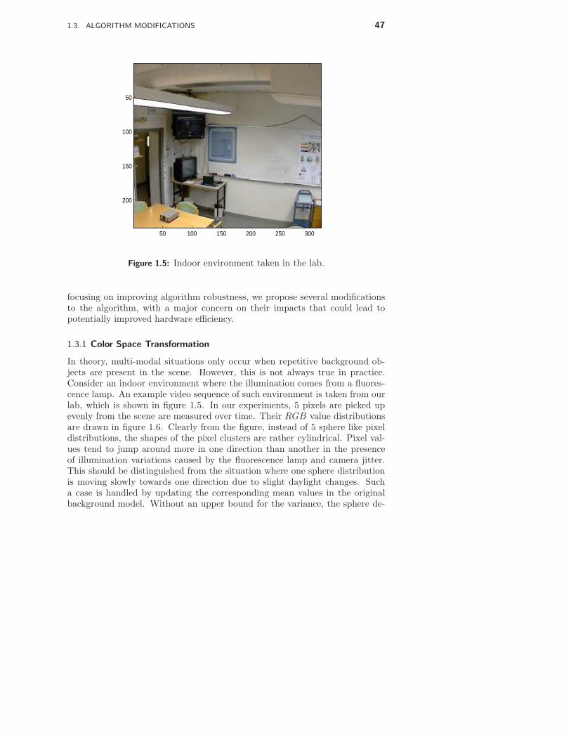
1.3. ALGORITHM MODIFICATIONS 47
50 100 150 200 250 300
50
100
150
200
Figure 1.5: Indoor environment taken in the lab.
focusing on improving algorithm robustness, we propose several modificationsto the algorithm, with a major concern on their impacts that could lead topotentially improved hardware efficiency.
1.3.1 Color Space Transformation
In theory, multi-modal situations only occur when repetitive background ob-jects are present in the scene. However, this is not always true in practice.Consider an indoor environment where the illumination comes from a fluores-cence lamp. An example video sequence of such environment is taken from ourlab, which is shown in figure 1.5. In our experiments, 5 pixels are picked upevenly from the scene are measured over time. Their RGB value distributionsare drawn in figure 1.6. Clearly from the figure, instead of 5 sphere like pixeldistributions, the shapes of the pixel clusters are rather cylindrical. Pixel val-ues tend to jump around more in one direction than another in the presenceof illumination variations caused by the fluorescence lamp and camera jitter.This should be distinguished from the situation where one sphere distributionis moving slowly towards one direction due to slight daylight changes. Sucha case is handled by updating the corresponding mean values in the originalbackground model. Without an upper bound for the variance, the sphere de-

48 CHAPTER 1. SEGMENTATION
8090
100110
120
60
80
100
120
60
80
100
120
140
R
RGB SPACE
G
B
Figure 1.6: Five distributions in RGB color space.
scribing the distribution tends to grow until it covers nearly every pixel in themost distributed direction, thus taking up a large space such that most of itdoes not belong to the distribution (sphere A in figure 1.7). A simple solutionto work around this problem is to set an upper limit for the variance, e.g. themaximum value of the variance in the least distributed direction. The result ismulti-modal distributions represented as a series of smaller spheres (B-E in thesame figure). Although a background pixel distribution is modeled more pre-cisely by such a method, several Gaussian distributions are inferred which arehardware costly in terms of extra parameter updating and storage. In [27] D.Magee proposed a cylindrical model to address the issue, with primary axes ofall distribution cylinders pointing towards the origin. However, more parame-ters are needed for each cylindrical distribution than the spherical counterpart.The coordinates of a cylindrical system comprises distance, two angles and adiameter and the height. Furthermore, it is hardware costly computation totransform RGB values to cylindrical coordinates, e.g. division and square root.In addition, not every distribution cylinder is oriented towards the origin, seethe left middle distribution in figure 1.6.
To be able to model background pixels using a single distribution but with-out much hardware overhead, color space transformation is employed in ourimplementation. Both HSV and Y CbCr space were investigated, and their

1.3. ALGORITHM MODIFICATIONS 49
8085
9095
100105
60
70
80
90
10040
50
60
70
80
90
R
RGB SPACE
G
B
AB
C
D
E
Figure 1.7: A closer look of 2 Gaussian distributions on the bottom inthe left figure.
corresponding distributions are shown in figure 1.8and 1.9. By transformingRGB into Y CbCr space, the correlation among different color coordinates aremostly removed, resulting in nearly independent color components. With vary-ing illumination environment, only the Y component (intensity) varies accord-ingly, leaving Cb and Cr components (chromaticity) more or less independent.In [28], such feature is utilized for shadow reduction. Consequently, values ofthree independent components of a pixel in Y CbCr color space tends to spreadequally. As shown in figure 1.8, most pixel distributions are transformed fromcylinders back to spheres, capable of being modeled with a single distribu-tion. The transformation from RGB to Y CbCr is linear, and can be calculatedaccording to the following:
Y = 16 + 65.481× R + 128.553× G + 24.966× B (1.27)
Cb = 128 − 37.797× R − 74.203× G + 112.0 × B (1.28)
Cr = 128 + 112.0 × R − 93.786× G − 18.214× B. (1.29)
Only minor hardware overhead with a few extra multipliers and adders areintroduced, where multiplication with constant can be further utilized to reducehardware complexity. Simplifications can be performed to further reduce the

50 CHAPTER 1. SEGMENTATION
80
100
120110
120
130
140120
125
130
135
140
Cb
YCbCr SPACE
Y
Cr
Figure 1.8: 5 Sphere distributions in Y CbCr Space space.
0
0.2
0.4
0.6
0.8
1
0
0.2
0.4
0.6
0.8
10
0.05
0.1
0.15
0.2
0.25
0.3
0.35
0.4
0.45
0.5
H
HSV SPACE
S
V
Figure 1.9: Unpredictable distributions in HSV Space.

1.3. ALGORITHM MODIFICATIONS 51
Detection
MUX
Monitor
Parameter
Update
CMOSSensor
SensorInterface
RGB2YCbCr
NetworkSorting
MatchingLogic
VGAController
DDR SDRAM
Parameter
Coding &
Decoding
Foreground
FPGA
Figure 1.10: The conceptual block diagram of the segmentation unit.
number of multipliers to be 4 [29]. HSV color space, on the other hand, alsowith correlated coordinates, is no better than RGB color space if not worse.Unpredictable pixel clusters appeared occasionally as shown in figure 1.9, whichis impossible to model using Gaussian distributions.
1.3.2 Algorithm Simplifications
We propose two simplifications to the algorithm. In the original algorithmspecification, unbounded growing distribution will absorb more pixels. As aresult, the weight of that distribution will soon dominate all others. To over-come this, in [18], all updated Gaussian distributions are sorted according tothe ratio ω/σ. In this way, the distribution with dominant weight but largevariance does not get to the top, identified as background distribution. In ourapproach, with Y CbCr color space transformation, no upper bound is needed.All distributions can be simply sorted by their weights only, effectively elimi-nating division operations in the implementation.
Another simplification made in the process of foreground/background detec-tion is instead of using equation 1, the determination can be made by checkingthe weight of each distribution only. This is due to the fact that one pixel clus-ter will not spread out in several distributions by color space transformation toY CbCr. The equation that determines the background distribution is changedto
B = argmink (ωk > H) . (1.30)
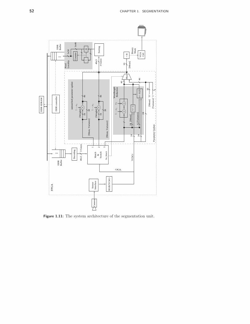
52 CHAPTER 1. SEGMENTATION
+/−
1
Mu
x
DD
R S
DR
AM
De
cod
ing
RG
B2
YC
bC
r
+/−
0.2
5
Se
nso
rIn
terf
ace
Wo
rdle
ng
thR
ed
uct
ion
>D
Co
un
ter So
rtin
g
VG
AC
trl
Pix
el
Lo
calit
y
Bin
ary
Ma
sk
> H
un
ma
tch
ed
pa
ram
ete
r u
pd
ate
[We
igh
t]
16
30
[We
igh
t]
46
Ca
me
ra
DD
RB
uffe
r
DD
RB
uffe
r
Ma
tch
&S
witc
h
DD
R c
on
tro
ller
24
24
[Me
an
]2
4 6[V
aria
nce
]4
6
46
24
16
’0’
’1’
6[V
aria
nce
]
[Me
an
]
3 G
au
ss4
6x3
FP
GA
No
_M
atc
h
YC
bC
r
Pa
ram
ete
r U
pd
ate
YCbCr
3 G
au
ss
46
x3
3x5
0
3x4
6
[Me
an
]
16
1 32
[Me
an
, V
aria
nce
]
[Me
an
, V
aria
nce
]
16
30
46
α1
1−
α1
1−
α1
1−
α1
Figure 1.11: The system architecture of the segmentation unit.

1.4. HARDWARE IMPLEMENTATION OF SEGMENTATION UNIT 53
This results in automatic single or multi modal background model withouthaving to adjust the value of H.
1.4 Hardware Implementation of Segmentation Unit
To perform the algorithm with VGA resolution in real-time, a dedicated hard-ware architecture, with a streamlined data flow and memory bandwidth reduc-tion schemes, is implemented to address the computation capacity and memorybandwidth bottlenecks. Algorithm modifications covered in previous sectionsare implemented with potential benefits on hardware efficiency and segmenta-tion quality. This is a large improvement to the previous work [30], where only352×288 resolution is achieved without any memory reduction schemes andalgorithm modifications. In this section, a thorough description of the wholesystem architecture of the segmentation unit is given, followed by detailed dis-cussions on memory reduction schemes.
To help for a better understanding of the architecture, a simplified con-ceptual block diagram of the whole system is given in figure 1.10 to illustratethe dataflow within the system. From the figure, the whole system starts withCMOS image sensor capturing video sequence in real-time and feeding it tothe system through a sensor interface. The interface is designed to be able tocontrol the parameters of the image sensor on run-time, e.g. analog gain andintegration time, so that better image quality can be obtained within differentenvironments. The sensor interface is also responsible for sampling the imagedata transferred from off-chip. In our implementation, an over sampling schemeby higher clock frequency (100Mhz) is used to ensure the accuracy of the imagedata. The image data is captured with one color component at a time, andthree complete color components are sent to the system after serial-paralleltransform. To handle different clock frequencies, input FIFOs, implemented asdistributed RAMs, are used to interface to both the segmentation logic and theVGA controller where the original video data can be monitored on a screen.The image data from the sensor are RGB values, and need to be converted intoY CbCr components before entering the segmentation logic block according tothe algorithm modification above. Each pixel has a series of correspondingGaussian distributions, where are stored on off-chip memories (DDR SDRAM)due to its size. With all the Gaussian parameters read from the DDR SDRAMand decoded by the parameter encoder/decoder, a match is calculated in thematching logic block to check if the incoming pixel matches any of the exist-ing distributions. The match and switch block is composed of mainly com-parators and multiplexer so that any the matching Gaussian parameters aremultiplexed to a specific output port. The output from the matching block isreordered Gaussian distributions with the matching distribution switched to aspecific port. The Gaussian distributions are updated according to the algo-

54 CHAPTER 1. SEGMENTATION
rithm modifications mentioned above, from where the foreground/backgrounddetection can start by checking the weight of the updated matched Gaussiandistribution. The output is a binary stream to be multiplexed to the monitor,indicating foreground and background pixels with white and black colors. Theupdated Gaussian parameters have to be sorted for use in the next frame, andall distributions should be ordered according to their weight. This is imple-mented in a dedicated sorting network that will be covered in more details inthe following section. To reduce heavy memory bandwidth incurred by access-ing off-chip DDR SDRAM that stores one frame of Gaussian distributions, anencoding/decoding block is designed by utilizing pixel localities in succeedingneighboring pixels. This is covered in more detail in Section 1.4.3.
In the following sections, implementation details of the architecture shownin figure 1.11 are explained with an emphasis on the parts with algorithm mod-ifications, which are indicated by shaded area. From the figure, with the imagedata captured and transformed into Y CbCr color space as explained earlier,the match and switch block tries to match the incoming pixel with Gaussiandistributions taken from the previous frame. To avoid the competition sev-eral Gaussian distributions matching the incoming pixel, only the one withhighest likelihood (large weight) is selected as the matching distribution. Amatched Gaussian is switched to the bottom(3 in the figure). In case no matchis found, a No match signal is asserted for use in later blocks. Dependingon if there is a match for a distribution, each distribution is updated accord-ingly. For the matched Gaussian distribution, a proposed updating schemeis implemented with only adders/subtractors for the mean and variance val-ues. Depending on whether the incoming Y CbCr value is larger than the meanvalues, a addition or subtraction is applied for parameter updating. Similarupdating schemes are utilized for variance update. The proposed parameterupdate results in low hardware complexity by replacing the hardware costlyoperations in equation1.20 and 1.21, e.g. square and multiplication with largewordlength with incrementors/decrementors. Other benefits of the proposedupdating schemes are described in detail in section 1.4.2. For the case that nomatch is found, a MUX is used together with a No match signal to update allparameters for the distribution (3 in the figure) with predefined values.
1.4.1 Sorting
The updated Gaussian parameters have to be sorted for use in the next frame.In order to reduce hardware complexity found in parallel sorting networks,such as [31] [32] [33], while still maintaining the speed, a specific feature inthe algorithm is explored. By observing that only one Gaussian distribution isupdated at a time and all the distributions are initially sorted, the sorting ofN Gaussian distributions can be changed to rearranging an updated distribu-
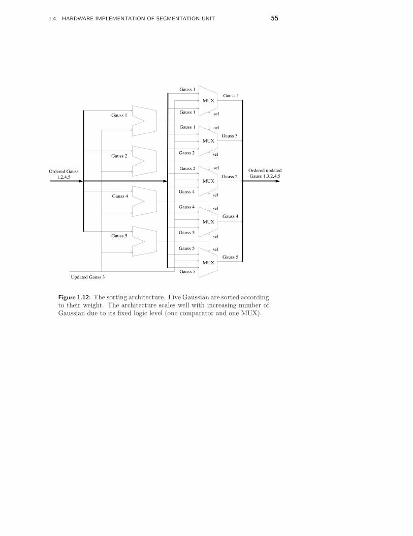
1.4. HARDWARE IMPLEMENTATION OF SEGMENTATION UNIT 55
MUX
MUX
MUX
MUX
MUX
MUX
MUX
MUX
MUX
Gauss 1
Gauss 2
Gauss 4
Gauss 5
Updated Gauss 3
Ordered Gauss
1,2,4,5
sel
sel
sel
sel
sel
sel
sel
sel
Ordered updated
Gauss 1,3,2,4,5
Gauss 1
Gauss 5
Gauss 4
Gauss 2
Gauss 3
Gauss 1
Gauss 1
Gauss 1
Gauss 2
Gauss 2
Gauss 5
Gauss 5
Gauss 4
Gauss 4
Gauss 5
Figure 1.12: The sorting architecture. Five Gaussian are sorted accordingto their weight. The architecture scales well with increasing number ofGaussian due to its fixed logic level (one comparator and one MUX).
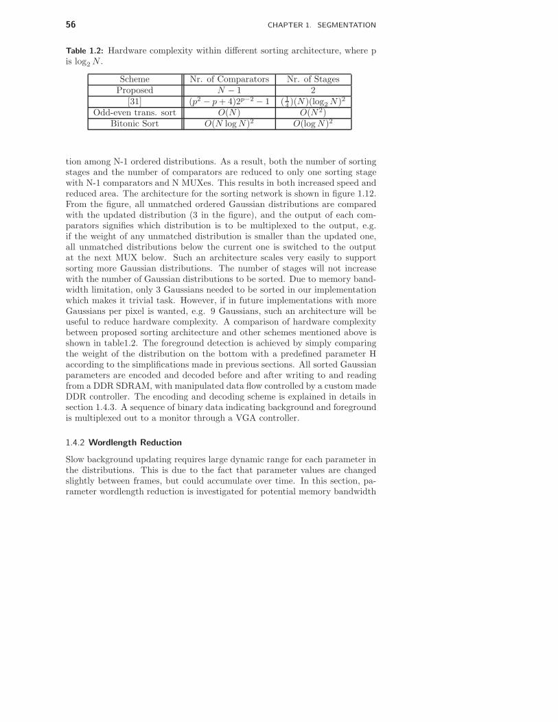
56 CHAPTER 1. SEGMENTATION
Table 1.2: Hardware complexity within different sorting architecture, where pis log2 N .
Scheme Nr. of Comparators Nr. of StagesProposed N − 1 2
[31] (p2 − p + 4)2p−2 − 1 (14 )(N)(log2 N)2
Odd-even trans. sort O(N) O(N2)Bitonic Sort O(N log N)2 O(log N)2
tion among N-1 ordered distributions. As a result, both the number of sortingstages and the number of comparators are reduced to only one sorting stagewith N-1 comparators and N MUXes. This results in both increased speed andreduced area. The architecture for the sorting network is shown in figure 1.12.From the figure, all unmatched ordered Gaussian distributions are comparedwith the updated distribution (3 in the figure), and the output of each com-parators signifies which distribution is to be multiplexed to the output, e.g.if the weight of any unmatched distribution is smaller than the updated one,all unmatched distributions below the current one is switched to the outputat the next MUX below. Such an architecture scales very easily to supportsorting more Gaussian distributions. The number of stages will not increasewith the number of Gaussian distributions to be sorted. Due to memory band-width limitation, only 3 Gaussians needed to be sorted in our implementationwhich makes it trivial task. However, if in future implementations with moreGaussians per pixel is wanted, e.g. 9 Gaussians, such an architecture will beuseful to reduce hardware complexity. A comparison of hardware complexitybetween proposed sorting architecture and other schemes mentioned above isshown in table1.2. The foreground detection is achieved by simply comparingthe weight of the distribution on the bottom with a predefined parameter Haccording to the simplifications made in previous sections. All sorted Gaussianparameters are encoded and decoded before and after writing to and readingfrom a DDR SDRAM, with manipulated data flow controlled by a custom madeDDR controller. The encoding and decoding scheme is explained in details insection 1.4.3. A sequence of binary data indicating background and foregroundis multiplexed out to a monitor through a VGA controller.
1.4.2 Wordlength Reduction
Slow background updating requires large dynamic range for each parameter inthe distributions. This is due to the fact that parameter values are changedslightly between frames, but could accumulate over time. In this section, pa-rameter wordlength reduction is investigated for potential memory bandwidth

1.4. HARDWARE IMPLEMENTATION OF SEGMENTATION UNIT 57
0 200 400 600 800 1000 1200 14000
10
20
30
40
50
60
70
80
90
100
zoom in area
(a) The original parameter updating scheme in presence of relatively fast lightchanges. Red color component values (solid line) of a pixel over frames are plottedtogether with updated mean values for the red color channel (diamond line).
120 140 160 180 200 220 240 260 280 300
45
50
55
60
65
70
75
(b) A closer look at the zoom in area in the the figure above.
Figure 1.13: The results from the original parameter updating scheme.

58 CHAPTER 1. SEGMENTATION
0 200 400 600 800 1000 1200 14000
10
20
30
40
50
60
70
80
90
100
zoom in area
(a) The proposed parameter updating scheme in presence of relatively fast lightchanges. Red color component values (solid line) of a pixel over frames are plottedtogether with updated mean values for the red color channel (star line).
180 200 220 240 260 280
44
46
48
50
52
54
56
58
60
62
64
(b) A closer look at the zoom in area in the figure above
Figure 1.14: The results from the proposed parameter updating schemes.
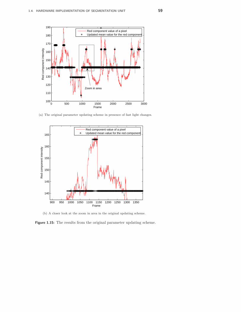
1.4. HARDWARE IMPLEMENTATION OF SEGMENTATION UNIT 59
0 500 1000 1500 2000 2500 3000100
110
120
130
140
150
160
170
180
190
Frame
Red
com
pone
nt in
tens
ity
Red component value of a pixelUpdated mean value for the red component
Zoom in area
(a) The original parameter updating scheme in presence of fast light changes.
900 950 1000 1050 1100 1150 1200 1250 1300 1350
140
145
150
155
160
165
Frame
Red
com
pone
nt in
tens
ity
Red component value of a pixelUpdated mean value for the red component
(b) A closer look at the zoom in area in the original updating scheme.
Figure 1.15: The results from the original parameter updating scheme.
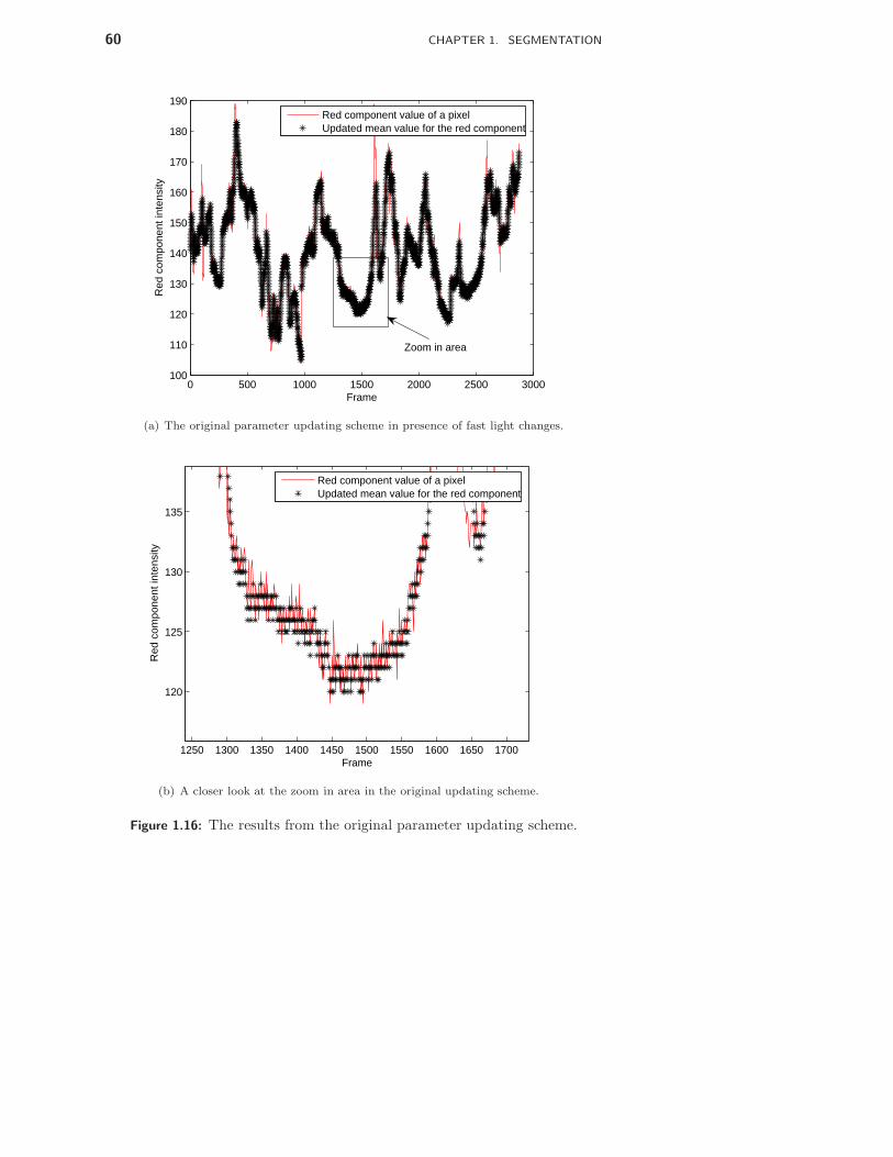
60 CHAPTER 1. SEGMENTATION
0 500 1000 1500 2000 2500 3000100
110
120
130
140
150
160
170
180
190
Frame
Red
com
pone
nt in
tens
ity
Red component value of a pixelUpdated mean value for the red component
Zoom in area
(a) The original parameter updating scheme in presence of fast light changes.
1250 1300 1350 1400 1450 1500 1550 1600 1650 1700
120
125
130
135
Frame
Red
com
pone
nt in
tens
ity
Red component value of a pixelUpdated mean value for the red component
(b) A closer look at the zoom in area in the original updating scheme.
Figure 1.16: The results from the original parameter updating scheme.

1.4. HARDWARE IMPLEMENTATION OF SEGMENTATION UNIT 61
0 500 1000 1500 2000 2500 30000
20
40
60
80
100
120
140
Frame
Red
com
pone
nt in
tens
ity
Red component value of a pixelUpdated mean value for the red component
Zoom in area
(a) The original parameter updating scheme in presence of minor light changes.
1100 1200 1300 1400 1500 1600 1700
110
112
114
116
118
120
122
124
126
Frame
Red
com
pone
nt in
tens
ity
Red component value of a pixelUpdated mean value for the red component
(b) A closer look at the zoom in area in the original updating scheme.
Figure 1.17: The results from the original parameter updating scheme.

62 CHAPTER 1. SEGMENTATION
0 500 1000 1500 2000 2500 30000
20
40
60
80
100
120
140
Frame
Red
com
pone
nt in
tens
ity
Red component value of a pixelUpdated mean value for the red component
Zoom in area
(a) The original parameter updating scheme in presence of minor light changes.
1200 1300 1400 1500 1600 1700 1800
114
116
118
120
122
124
126
Frame
Red
com
pone
nt in
tens
ity
Red component value of a pixelUpdated mean value for the red component
(b) A closer look at the zoom in area in the original updating scheme.
Figure 1.18: The results from the original parameter updating scheme.

1.4. HARDWARE IMPLEMENTATION OF SEGMENTATION UNIT 63
reduction.According to equations 1.20 and 1.21, the mean and variance of a Gaussian
distribution is updated using a learning factor ρ. The difference of mean andvariance between current and previous frame is derived from the equation as
∆µ = µt − µt−1 = ρ(Xt − µt−1) and (1.31)
∆σ2 = σ2t − σ2
t−1 = ρ((Xt − µt)T (Xt − µt) − σ2
t−1). (1.32)
Given a small value for ρ, e.g. 0.0001, a unit difference between the incomingpixel and the current mean value results in a value of 0.0001 for ∆µ. To be ableto record this slight change, 22 bits have to be used for the mean value, where 14bits accounts for the fractional part and 8 bits are used for the integer one. Lessbits can be achieved by ignoring small deviations of the incoming pixel fromcurrent mean, while picking up only large ones. The extreme case is when onlythe largest deviation is picked, e.g. where the incoming pixel is in the range of Jtimes standard deviation off the current mean. Larger than that, the incomingpixel will not match the current distribution. With an upper bound for thevariance, e.g. 16, a maximum value of 0.0001×2.5×
√16 = 0.001 is derived for
∆µ, which can be represented by 10 bits. Using a wordlength lower than that,no changes would be recorded ever. In practice, the bits for fractional partsshould be somewhere in the range of 10-14 bits. With similar calculations, 7-14bits are obtained for the fractional parts of the variance. Together with 16 bitsweight and integer parts of the mean and the variance, 81-100 bits are neededfor a single Gaussian distribution. To reduce this number, a wordlength re-duction scheme is proposed. From equation 1.31, a small positive or negativenumber is derived depending on whether the incoming pixel is larger than thecurrent mean. Instead of adding a small positive or negative fractional numberto the current mean, a value of 1 or -1 is added. The overshooting caused bysuch coarse adjustment could be compensated by the update in the next frame,e.g. without illumination variation, the mean value will fluctuate with a mag-nitude of 1. This is negligible since Gaussian distribution is usually a spherewith a diameter of more than 10 from our experiment data. In a relatively fastvarying illumination environment, e.g. 25 RGB value changes in a second, fastadaptation to new lighting conditions is also enabled by adding or subtractingones in consecutive frames. Figure 1.14(a) shows the experimental results ofthe coarse updating in a varying lighting room, where the light is manuallyturned up and down. The parameter updating scheme specified in the originalalgorithm is also drawn in figure 1.13(a) for comparison. A closer look of thetwo schemes are given in figure 1.14(b) and 1.13(b). From figure 1.13(a)and 1.13(b), it is clear that parameter updating does not work well in thepresence of fast light changes. As slow parameter updating (diamond line inthe figure) for each Gaussian distribution will not keep track of the pixel value

64 CHAPTER 1. SEGMENTATION
changes (solid line in the figure) in fast light changing environment, that Gaus-sian distribution will finally not be able to match the incoming pixel values, inwhich case Gaussian distribution replacement takes place in stead of parameterupdating. The coarse updating scheme on the other hand relieves the prob-lem to certain extent, where consecutive ones are added or subtracted to keeptrack of the relatively fast changes. Similar results are obtained from two othertest sequences, namely scene “trees” and “parklot” which are shown in figure1.22(a) and 1.23(a). These two scenes are both taken in outdoor environments.Scene “trees” records many relatively fast light changes due to it is dynamicbackground, and scene “parklot” consists of nearly constant illumination con-dition. The results from both parameter updating schemes for both sequencesare shown in figure 1.15,1.16, 1.17 and 1.18. From these figures, it can beseen that the proposed coarse updating scheme works fine in both situations.It keeps track of the relatively fast value changes in the dynamic scene whilefluctuates around a constant value in the latter static scene. However, withthe primary goal to reduce wordlength, the coarse parameter updating schemeresults in limited improvements to the segmentation results. Nearly no visualdifference can be observed in the segmented results from the two schemes.
With coarse updating, only integers are needed for mean specification,which effectively reduce the wordlength from 18 − 22 down to 8 bits. Similarapproach can be applied to the variance (a step value of 0.25 is used instead),resulting in a wordlength of 6 bits, where 2 bits account for fractional part.Together with the weight, the wordlength of a single Gaussian distribution canbe reduced from 81 − 100 to only 44 bits, over 43% reduction is accomplishedeven compared to the extreme case mentioned above in the normal updatingscheme, where only 81 bits are used for each Gaussian distribution. In addi-tion, less hardware complexity is achieved as a bonus since multiplication withthe learning factor of ρ is no longer needed.
Thus, the proposed scheme enhance the algorithmic performance while atthe same time reduce both memory bandwidth and computational complexity.
1.4.3 Pixel Locality
In addition to wordlength reduction, a data compression scheme for furtherbandwidth reduction is proposed by utilizing pixel locality for Gaussian dis-tributions in adjacent areas. We classify “similar” Gaussian distributions inthe following way: from the definition of a matching process, each Gaussiandistribution can be simplified as a three dimensional cube instead of a spherein the Y CbCr color space. The center of the cube is composed of Y CbCr meanvalues whereas the border to the center is specified by J times variance. Oneway to measure the similarity between two distributions is to check how muchof the two cubes that overlap. If the overlap volume takes up certain percent-

1.4. HARDWARE IMPLEMENTATION OF SEGMENTATION UNIT 65
2.5 x sigma
R
mean
B
G
Cube overlap
Figure 1.19: Gaussian distribution similarity as modeled by cube overlapping.
age of both Gaussian cubes, they are regarded as “similar”. The whole idea isillustrated in figure 1.19. The reason for such a criteria lies in the fact thata pixel that matches one distribution will most likely match the other, if theyhave enough overlapping volume. The percentage is a threshold parameter thatcan be set to different values among different situations.
In the architecture, two similar distributions are treated as equivalent. Byonly saving non overlapping distributions together with the number of equiva-lent succeeding distributions, memory bandwidth is reduced. Various thresholdvalues are selected to evaluate the efficiency for memory bandwidth reduction.
Table 1.3: Design Summary
FPGA Utilization
Nr. of Slices Nr. of Flip Flops Nr. of DCMs Nr. of BRAMs6107 4273 5 84
Clock Domains
100Mhz 16Mhz 25MhzSensor interface & DDR controller Segmentation VGA controller
System Parameters
Resolution Throughput Frame rate Nr. of Gaussians640 × 480 170MB/s 25 3

66 CHAPTER 1. SEGMENTATION
50 100 150 200 250 300
50
100
150
200
(a) Scene “stairs”
0 500 1000 1500 2000 2500 30000.55
0.6
0.65
0.7
0.75
0.8
0.85
0.9
0.95
1
Frame
Mem
ory
BW
red
uctio
n
0.50.60.70.80.9
(b) Memory reduction in Scene stairs
Figure 1.20: Memory reduction results tested in Scene “stairs”. Videosequences are provided by AXIS Communications [34].
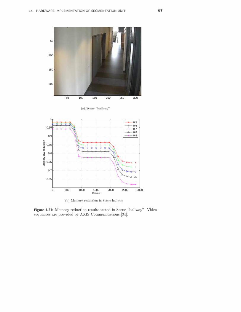
1.4. HARDWARE IMPLEMENTATION OF SEGMENTATION UNIT 67
50 100 150 200 250 300
50
100
150
200
(a) Scene “hallway”
0 500 1000 1500 2000 2500 3000
0.65
0.7
0.75
0.8
0.85
0.9
0.95
1
Frame
Mem
ory
BW
red
uctio
n
0.50.60.70.80.9
(b) Memory reduction in Scene hallway
Figure 1.21: Memory reduction results tested in Scene “hallway”. Videosequences are provided by AXIS Communications [34].

68 CHAPTER 1. SEGMENTATION
50 100 150 200 250 300
50
100
150
200
(a) Scene “trees”
0 500 1000 1500 2000 2500 3000
0.65
0.7
0.75
0.8
0.85
0.9
0.95
1
Frame
Mem
ory
BW
red
uctio
n
0.50.60.70.80.9
(b) Memory reduction in Scene trees
Figure 1.22: Memory reduction results tested in Scene “trees”. Videosequences are provided by AXIS Communications [34].
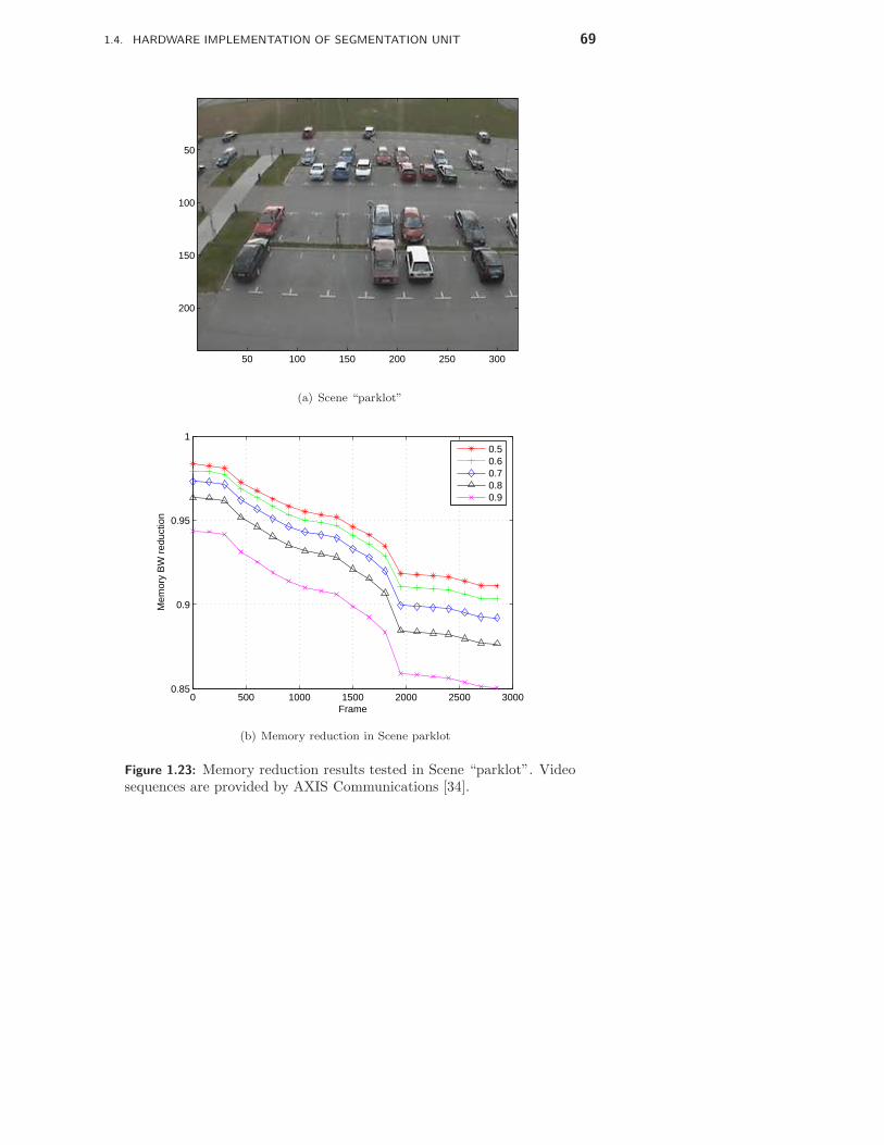
1.4. HARDWARE IMPLEMENTATION OF SEGMENTATION UNIT 69
50 100 150 200 250 300
50
100
150
200
(a) Scene “parklot”
0 500 1000 1500 2000 2500 30000.85
0.9
0.95
1
Frame
Mem
ory
BW
red
uctio
n
0.50.60.70.80.9
(b) Memory reduction in Scene parklot
Figure 1.23: Memory reduction results tested in Scene “parklot”. Videosequences are provided by AXIS Communications [34].

70 CHAPTER 1. SEGMENTATION
0 500 10000.45
0.5
0.55
0.6
0.65
0.7
0.75
0.8
0.85
0.9
0.95
Frame
Mem
ory
band
wid
th re
duct
ion
0.90.80.70.60.5
0.5 0.6 0.7 0.8 0.90.45
0.5
0.55
0.6
0.65
0.7
0.75
Thresholdm
emor
y ba
ndw
idth
redu
ctio
n
Figure 1.24: Memory bandwidth reductions achieved in the video se-quences from our lab. Left: memory bandwidth reduction over frames.Right: Memory bandwidth reduction over threshold value.
Figure 1.25: The results before and after morphological filtering for differ-ent thresholds: (left) Original result, (middle) Threshold of 0.8, (right)Threshold of 0.4.

1.5. SYSTEM INTEGRATION AND FPGA PROTOTYPE 71
With a low threshold value where less overlapping Gaussian distributions areregarded as the same, more savings could be achieved. However, more noiseis generated due to increasing mismatches in the matching block. Fortunately,such noise is found non-accumulating and therefore can be reduced by latermorphological filtering [35]. Figures 1.20,1.21,1.22,1.23 show the memorybandwidth savings over frames with various threshold values. The simula-tion results are obtained from matlab, with four video sequences provided byAXIS [34] are evaluated for both indoor and outdoor scenes. The sequences areselected to reflect a range of real-world background environments with possibledifficulties for many segmentation and tracking algorithms. The scene “stairs”comprises people moving up and down the stairs randomly. Gradual illumi-nation changes together with shadows are the major disturbing factors. Thescene “hallway” focus on the scenarios with people moving closer or furtheraway from the camera. The foreground object size is varying over time. Thescene “trees” address the issue of quasi-static environments where a swayingtree is present as the dynamic background object. The scene “parklot” presentsa environment with walking people, moving cars of different size. Gradual illu-mination as well as waking foreground object are also within the focus. It canbe seen from the sequences, memory reductions scheme works robustly withindifferent real-world environments with variation only in the beginning due tovaried foreground actives. During initialization phase, only background pixelsare present, which exhibit high similarity within neighboring pixels. With fore-ground objects entering the scene, part of Gaussian distributions are replaced,which results in the decrease of number of similar Gaussian distributions. Thetrends will continue until it reaches a certain point where most pixel locationscontains a foreground distribution. The decrease will flattens out in the endsince more foreground objects always replace the distribution that representa foreground pixel. Foreground objects activities can vary in different videoscenes, e.g. continuous activities in figure 1.20(a) where people going up anddown the stairs all the time, and the two peak activity periods around frames600− 900 and frames 2100− 2500 in figure 1.21(a), where people walking by intwo discrete time period. In the long run, the bandwidth savings tends to sta-bilize (around 50%−75% depending on threshold value) after the initializationphase. Another test sequence is also experimented in our lab. Similar resultsare observed as shown in figure 1.24. The quality of segmentation results beforeand after morphology are shown in figure 1.25, where it is clear that memoryreduction comes at the cost of segmentation quality. Too low threshold valueresults in clustered noises that would not be filtered out by morphological fil-tering. In this implementation, a threshold value of 0.8 is selected, combinedwith wordlength reduction scheme, a memory bandwidth reduction of over 70%is accomplished. To evaluate long term effects of memory bandwidth reductionscheme, FPGA platform is required to collect data in real time.

72 CHAPTER 1. SEGMENTATION
Table 1.4: Hardware complexity for different blocks within segmentation unit.
Logic Block Nr. of Slices (%) Nr. Block RAMsMatch 253 (4%) 0Switch 652 (11%) 0
Parameter Update 483 (8%) 0Pixel Locality 1530 (25%) 0
Sensor Interface 540 (9%) 3Sorting 355 (6%) 0
DDR controller 1599 (26%) 24RGB2Y CbCr 181 (3%) 0
VGA controller 377 (6%) 57
1.5 System Integration and FPGA Prototype
The segmentation unit is prototyped in an Xilinx VIrtexII vp30 developmentboard, as shown in figure 1.26. The board come with one DDR memory slotwith customized on board signal traces that minimizes the skew between differ-ent signals. Virtex II vp30 is equipped with two on-chip PowerPC embeddedprocessor cores. The number of on-chip block RAMs is 136, with 2448 Kb intotal. A custom-made PCB extension board is mounted on the FPGA boardto support image data read in through a image sensor. A dedicated VGA con-troller is developed streaming output data into a monitor, where the resultsfrom different stage of the logic can be monitored. Detailed description of thesystem integration of the whole tracking system is covered in the next chapter.In table 1.4, a summary of the hardware complexities of different blocks in thesegmentation is given. It can be seen that algorithm modifications results in alow hardware complexity in parameter updating block, which merely occupies8% of the total utilized resources. However, memory reduction scheme withpixel locality incurs relatively costly in hardware, where many multiplicationsare needed to calculate the cube volumes. DDR controller contributes to alarge part of the whole design resources, due to complicated memory commandand data signal manipulations, clock schemes, and buffer controls. The hard-ware complexity of sorting and color space transformation is low by after op-timizations. VGA controller consumes most of the on-chip memory resources.Dual-port block RAMs are used as video RAMS in the VGA controller, whichare shared by different blocks of the whole surveillance system to display theresults from different stages on a monitor . Block RAMs are also used as databuffers to support DDR burst read and write operations.

1.7. CONCLUSIONS 73
Figure 1.26: FGPA prototypes.
1.6 Results
The system is implemented on a Xilinx VirtexIIpro vp30 FPGA [36] develop-ment board as shown in figure 1.26. The whole design is partitioned into 3clock domains for different blocks, and asynchronous FIFOs are used to inter-face blocks working with different clocks. A KODAK KAC-9648 CMOS sen-sor [37] is used to capture color images stream into the FPGA platform. Realtime segmentation performance is achieved on video sequences with 3 Gaussiandistributions per pixel. With the proposed memory reduction schemes, off-chipmemory bandwidth is reduced by more than 70%. A summary of the wholedesign is given in Table 1.3.
1.7 Conclusions
A Real-time video segmentation unit is implemented on an Xilinx VirtexIIFPGA platform, serving as a real-time testbench for evaluating long term ef-fects of the corresponding algorithm. The segmentation unit is an importantpart of the whole tracking system developed at the department. With realtime performance, tracking schemes can be evaluated in varied environments

74 CHAPTER 1. SEGMENTATION
for system robustness testing . Software/hardware partition is facilitated in anFPGA platform, where high level operations e.g. features extraction in a track-ing algorithm can be implemented in software. The calculation and memoryintensive tasks e.g. segmentation, morphology are left to customized hardwarearchitecture. For the implementation of the hardware units, memory usage isidentified as the main bottleneck of the whole system, which is is common inmany image processing systems. This is especially true for segmentation sincemost algorithms operates in pixel-wise structures. To address the issue a jointmemory reduction scheme is proposed by utilizing pixel locality and wordlengthreduction. By measuring similarity of neighboring gaussian distributions withoverlapping volume of two cubes, threshold can be set to classify Gaussiansimilarities. Wordlength reduction is as important for memory bandwidth re-duction. By utilizing coarse parameter updating scheme, wordlength for eachGaussian parameters is reduced by more than 43%, which effectively decreasethe memory bandwidth to off-chip memories. The substantial bandwidth re-duction comes at the cost of segmentation quality. By setting a threshold valueto a low value, noise generated can not be removed by morphology operation.Careful tradeoffs should be made based on different application environments.Algorithm modifications are of great importance for the efficiency of the hard-ware implementation. By utilizing Y CbCr color space, several simplificationscan be made that results in potential hardware savings.
Chapter 2
System Integration of Automated Video Surveil-
lance System
In this chapter, an original paper is presented for system integration of a real-time video surveillance embedded system:
Fredrik Kristensen, Hugo Hedberg, Hongtu Jiang, Peter Nilsson, and Vik-tor Owall, ”Hardware Aspects of a Real-Time Surveillance System” , inProc. of The Sixth IEEE International Workshop on Visual Surveillance.
The author’s contribution is on the segmentation part. Many parts of thepaper have been changed since the publication. This work is currently beingupdated and revised. A journal paper is in preparation to be submitted inFebruary, 2007.
75

76CHAPTER 2. SYSTEM INTEGRATION OF AUTOMATED VIDEO SURVEILLANCE
SYSTEM
Abstract
This paper presents the implementation of an automated digital video surveil-lance system for real-time performance on an embedded platform. To achievereal-time performance, the system includes hardware accelerators for videosegmentation, morphological operations, labeling and feature extraction whiletracking is handled in software. By implementing a complete system on anembedded platform, bottlenecks in computational complexity and memory re-quirements can be identified and addressed. A memory access reduction schemefor the video segmentation part that utilizes pixel locality is proposed whichshows the potential of reducing accesses with >60%. It is also shown how alow-complexity addition to the segmentation rule can reduce the affect of shad-ows. Furthermore, a low complexity morphology architecture with low memoryrequirements is presented together with a labeling unit based on a contour trac-ing technique. The system is running in real-time at an FPGA developmentboard with a resolution of 320×240 at 25 frames per second.
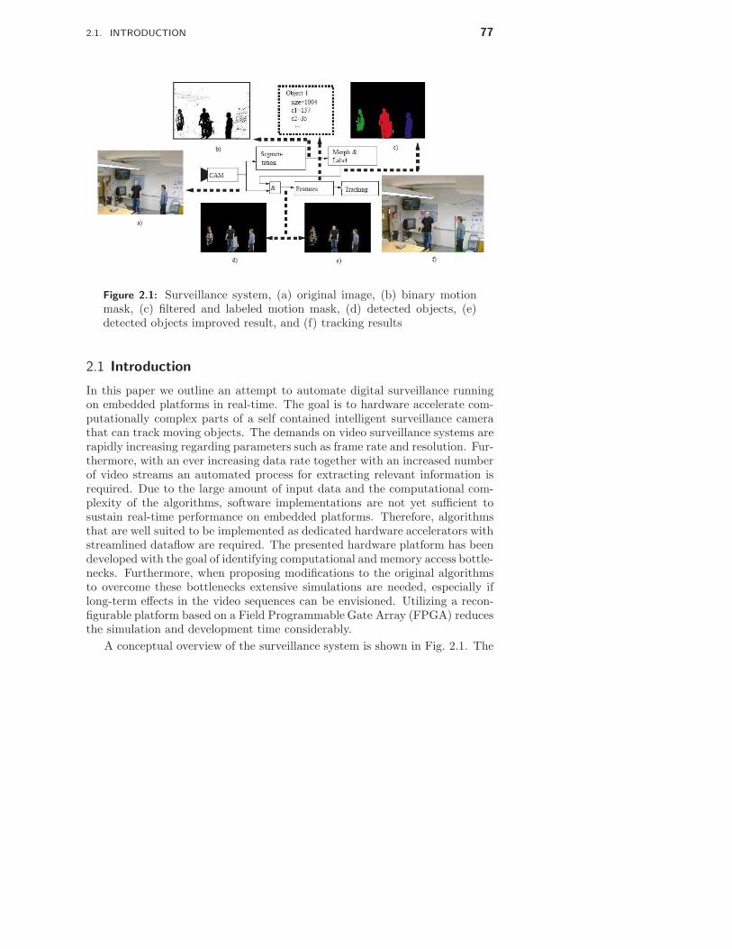
2.1. INTRODUCTION 77ts
Figure 2.1: Surveillance system, (a) original image, (b) binary motionmask, (c) filtered and labeled motion mask, (d) detected objects, (e)detected objects improved result, and (f) tracking results
2.1 Introduction
In this paper we outline an attempt to automate digital surveillance runningon embedded platforms in real-time. The goal is to hardware accelerate com-putationally complex parts of a self contained intelligent surveillance camerathat can track moving objects. The demands on video surveillance systems arerapidly increasing regarding parameters such as frame rate and resolution. Fur-thermore, with an ever increasing data rate together with an increased numberof video streams an automated process for extracting relevant information isrequired. Due to the large amount of input data and the computational com-plexity of the algorithms, software implementations are not yet sufficient tosustain real-time performance on embedded platforms. Therefore, algorithmsthat are well suited to be implemented as dedicated hardware accelerators withstreamlined dataflow are required. The presented hardware platform has beendeveloped with the goal of identifying computational and memory access bottle-necks. Furthermore, when proposing modifications to the original algorithmsto overcome these bottlenecks extensive simulations are needed, especially iflong-term effects in the video sequences can be envisioned. Utilizing a recon-figurable platform based on a Field Programmable Gate Array (FPGA) reducesthe simulation and development time considerably.
A conceptual overview of the surveillance system is shown in Fig. 2.1. The

78CHAPTER 2. SYSTEM INTEGRATION OF AUTOMATED VIDEO SURVEILLANCE
SYSTEM
camera feeds the image processing system with a real-time image stream of25 frames per second (fps). A segmentation algorithm, in this case GaussianMixture background Model (GMM), preprocesses the image stream and pro-duces a binary mask in which zeros and ones correspond to background andforeground, respectively. In theory, only the moving parts of an image shouldbe distinguished as independent objects in the binary mask. However, in re-ality the mask will be distorted with noise and single objects are shattered,e.g., if parts of the moving object has the same color as the background. Inorder to remove noise and merge shattered objects, one or more morphologicaloperations are performed on the mask. These morphological operations willproduce a frame of connected clusters which have to be identified, i.e. labeled,and features should be extracted to be sent as input to the tracking algorithm.
The main bottlenecks of the segmentation algorithm, shared with manyother image based algorithms, are the high memory bandwidth and the overallmemory requirements. A reduced memory access scheme is proposed, whichintroduces coding of the Gaussian parameters using pixel locality. A reductionof >60% is indicated but results in increased noise in the binary mask. However,this noise is non-accumulating and can be reduced by the morphology operationat no extra cost. Long term effects of the memory reduction scheme as wellas more advanced version have to be further investigated. Furthermore, ithas been investigated how different color spaces affect the segmentation resultin terms of noise and shadow sensitivity. A low complexity and low memoryrequirement architecture for morphological operations is presented which allowsfor a larger number of such operations to be performed. In addition, a labelingunit based on a contour tracing technique is presented which extracts featuresat low extra cost.
Typical examples of intermediate results are shown in Fig. 2.1. In Fig. 2.1athe original image is shown and the segmented binary mask in Fig. 2.1b. Thelabeled objects are shown in Fig. 2.1c were we can notify that the noise hasbeen removed. By modifying the segmentation algorithm to be able to identifypotential shadows we see that these can be removed to a large extent, e.g. thelarge shadow attached to the lower right side of the mid-person as shown inFig 2.1d and e. Finally, Fig. 2.1f shows the output from the tracking algorithmwhere the objects are identified by the colored bounding boxes.
2.2 Segmentation
Compared to many other algorithms for video segmentation, one based onGaussian Mixture background Model (GMM) was proposed in [18] with theunique feature of robustness in multi-modal background scenarios. A GMMis required for modeling repetitive background object motion, for example,swaying trees, reflections on a lake surface, a flickering monitor, etc. A pixel

2.2. SEGMENTATION 79
located in the region where repetitive motion occurs will generally consist of twoor more background colors, i.e. the RGB value of that specific pixel togglesover time. This would result in false foreground object detection with mostother adaptive background estimation approaches.
The advantage of the GMM is achieved by updating several Gaussian pa-rameters for each pixel, imposing a computational complexity and high memorybandwidth that prohibit real-time performance using a general purpose com-puter. In our simulations, on an AMD 4400+ dual core processor, a frame rateof only 4-6 fps is achieved for video sequences with 320x240 resolution. For areal-time video surveillance system with higher resolution, hardware accelera-tion is required.
2.2.1 Algorithm formulation
The algorithm is briefly formulated as follows: Measured from consecutivevideo frames, the values of any pixel can be regarded as a Gaussian distribu-tion. Characterized by mean and variance values, the distribution representsa location centered at its mean values in the RGB color space, where the pixelvalue is most likely to be observed over frames. A pixel containing severalbackground object colors, eg. the leaves of a swaying tree and a road, can bemodeled with a mixture of Gaussian distributions with different weights. Theweight of each distribution indicates the probability of matching a new incom-ing pixel. A match is defined as the incoming pixel within certain deviationoff the center. In this paper, J times the standard deviation of the distirbu-tion is used as matching threshold [18], where J is 2.5. The higher the weightis, the more likely the distribution belongs to the background. Mathemati-cally, the portion of the Gaussian distributions belonging to the background isdetermined by
B = argminb
(
b∑
k=1
ωk > H
)
,
where H is a predefined parameter and ω is the weight. The mean, variance andweight factors are updated frame by frame. If a match is found, the matcheddistribution is updated as:
ωk,t = (1 − α)ωk,t + α, µt = (1 − ρ)µt−1 + ρXt
σ2 = (1 − ρ)σ2t−1 + ρ(Xt − µt)
T (Xt − µt);
where µ, σ2 are the mean and variance respectively, and α, ρ are learning fac-tors. For those unmatched, the weight is updated according to
ωk,t = (1 − α)ωk,t,

80CHAPTER 2. SYSTEM INTEGRATION OF AUTOMATED VIDEO SURVEILLANCE
SYSTEM
Sensor
interface
CMOSsensor
Matching
logic
Parameterupdate
Sorting
networkSegmented
binary stream
Sorted
Gaussian
parameters
Monitor
VGAController
morphology
XILINX FPGA
SortedGaussianparameters
Compressedparameters
DDR SDRAM
Foreground
detection
Parameter
Reforming
To
Figure 2.2: The system architecture of the segmentation unit.
while the mean and the variance remain the same. If none of the distributionsare matched, the one with the lowest weight is replaced by a distribution withthe incoming pixel value as its mean, a low weight and a large variance.
Maintaining a mixture of Gaussian distributions for each pixel is costly interms of both calculation capacity and memory storage, especially with largeframe size. To manage the RGB data from a video camera in real time, adedicated hardware architecture is developed with a streamlined data flow.The hardware architecture as shown in Fig. 2.2 is presented in [30] and brieflyexplained as follows: A pixel value is read into the matching logic block from thesensor together with all the parameters for the mixture of Gaussian distributionand a match is calculated. In case an incoming pixel matches several Gaussiandistributions, only the one with highest weight is selected as the matchingdistribution.
2.2.2 Hardware implementation
After the updated Gaussian parameters have been sorted foreground detectionis achieved simply by summing up the weights of all the Gaussian distributionsthat have a higher likelihood than the updated one. By comparing the sumwith a predefined parameter H, a sequence of binary data indicating backgroundand foreground is streamed out to both the morphology block and the VGAcontroller.
2.2.3 Memory bandwidth reduction
Slow background updating process requires high precision for each parameterin the distributions. This is due to the fact that parameter values are changed

2.2. SEGMENTATION 81
Frames Threshold
Mem
ory
BW
reductio
n
Mem
ory
BW
reductio
n
0.450.45
0.5
0.5
0.5
0.5
0.55
0.55
0.6
0.6
0.6
0.6
0.65
0.65
0.7
0.7
0.7
0.7
0.75
0.75
0.8
0.8
0.8
0.85
0.9
0.9
0.9
0.95
0 500 1000
Figure 2.3: Memory bandwidth reduction over frames is shown to the leftand memory bandwidth reduction versus different threshold is shown tothe right.
slightly at a time, but could accumulate over time. From C++ simulation, bothmean and variance for a Gaussian distribution in adjacent frames vary in theorder of 10−4 to record slight light changes. For a fixed number representation,28 bits are assigned to each RGB mean parameters and the variance takes 24bits. The weight (likelihood) for each Gaussian distribution is updated usinga learning factor. To avoid an over-segmentation effect with a fast learningfactor, 16 bits are used for the weight with a slow learning factor (eg. 0.0002).One Gaussian distribution consists of the weight together with 3 means and1 variance and contributes to 124 bits. For a video sequences with 320x240resolution, a total of 27 Mbit Gaussian parameter data have to be stored andupdated for each new frame, which is far beyond the on-chip memory resources.
In this paper, a data compression scheme is proposed which utilizes sim-ilarities for Gaussian distributions in adjacent areas. We classify ”similar”Gaussians in the following way: from the definition of a matching process, eachGaussian distribution can be regarded as a three dimensional cube in the RGBspace, where the center of the cube is composed of RGB mean values whereasthe border to the center is specified by J times variance. One way to measurethe similarity between two distributions is to check how much of the two cubesvolume that overlap. If the overlap volume takes up a certain percentage ofboth Gaussian cubes, they are regarded as ”similar”. The reason for such crite-ria lies in the fact that a pixel that matches to one distribution will most likelymatch to the other, if they have enough overlapping volume. The percentageis a threshold parameter that can be set to different values among differentsimulations.
In the architecture, two similar distributions are treated as equivalent. Byonly saving non overlapping distributions together with the number of equiva-lent succeeding distributions, memory bandwidth is reduced. From simulation

82CHAPTER 2. SYSTEM INTEGRATION OF AUTOMATED VIDEO SURVEILLANCE
SYSTEM
a) b) c)
Figure 2.4: The result before and after morphological filtering for differ-ent thresholds, (a) original result, (b) with 0.8, and (c) with 0.4 thresh-old.
in C++, various threshold values are selected to evaluate the efficiency for mem-ory bandwidth reduction. With a low threshold value where less overlappingGaussians are regarded as the same, more savings could be achieved. However,more noise is generated in the segmented image due to increasing mismatchesin the matching block. Fortunately, such noise is found non-accumulating andtherefore can be reduced by later morphological filtering. Fig. 2.3 shows thememory bandwidth savings over frames with various threshold values. Fromthe figure, large memory bandwidth savings (around 95%) are achieved fromthe start to approximately 380 frames, in which case no foreground object en-ters the scene and only one out of three Gaussian distributions are updated tocontain the background. With more foreground objects moving in and occu-pying a bigger part of the frame, the number of similar Gaussian distributionsdrops dramatically, but tends to stabilize after some time when most pixelscontains both foreground and background distributions. It is also shown inthe figure that low threshold, by relaxing the criteria of similarity, results inmore memory bandwidth savings. The quality of segmentation results beforeand after morphology is shown in Fig. 2.4. From these Figures, it is clearthat memory reduction comes at the cost of segmentation quality. Too lowthreshold value results in noise clusters that would not be filtered out by mor-phological filtering. In this implementation, a threshold value of 0.8 is selected,with memory bandwidth savings of around 60%. To evaluate long term ef-fects of memory bandwidth reduction scheme, FPGA platform is required tocollect data in real time. In future implementations, commonly used videocompression scheme such as transform coding using a DCT or DWT are underconsideration for further Gaussian parameter compressions.

2.2. SEGMENTATION 83
c)
Cr
Cb
b)X
Cr
Cb
X
X
X X
X
Cr
d)
Cb
X
X
XX
XX
XX
X
a)
Figure 2.5: The original result (a) and the result with three differentshadow detection rules (b,c,d) in the CbCr plane, where X is the storedmean of CbCr, five example points are shown for each rule. A new pixelpart of a potential shadow if it falls in the gray area and there is anegative change in the Y component.
2.2.4 Shadow reduction
One drawback with the Gaussian mixture model segmentation algorithm isthat it is sensitive to shadows and noise. Thus it has been investigated in[38] how different color spaces affect the segmentation result in terms of noiseand shadow sensitivity. The YCbCr color space was found to be best, due tonumeric stability and an independent brightness channel. The investigationwas conducted with the implementation aspects in mind, i.e. simple changesthat easily could be incorporated in the existing hardware.
To reduce the number of detected shadows, pixels that could be part of apotential shadow have to be recognized. Assuming white light, Y will alwaysbe smaller when shaded and that Cb and Cr will go towards the origin. Withthis information a simple rule for shadows can be formed; A potential shadowis found if a negative change is detected in Y and CbCr have moved slightlytowards origin, compared to the stored mean of YCbCr. In addition, a shadowis not detected if a too large negative change in Y is found. Without thislimit, a pixel that change color from white to black would be classified as ashadow which would result in a loss of sensitivity instead of a shadow reduction.Based on experimental results, a suitable indoor value for the maximum allowednegative change in Y is around 20-30% of the dynamic range of Y .
In the upper part of Fig. 2.5 three different rules for the CbCr plane todetect potential shadows are shown. All three assume that a negative changein Y has already been detected. The gray areas represent the part of the CbCr
plane where a new pixel is ruled to be a potential shadow. The area location

84CHAPTER 2. SYSTEM INTEGRATION OF AUTOMATED VIDEO SURVEILLANCE
SYSTEM
is based on the stored mean of Cb and Cr, five example points are shown foreach rule. With the first rule a new pixel is part of a potential shadow if thesum of absolute differences in CbCr is less than a threshold. The second rulecompares the difference in Cb and Cr separately to thresholds that depend onthe position of the stored mean of Cb, Cr. The last rule allows changes in asmall sector from origin or, if the values are close to origin, in a small boxaround the stored mean of Cb, Cr [39]. The segmentation result with the threedifferent shadow rules are shown in Fig. 2.5. As seen, most of the shadowsare removed compared to Fig. 2.5a, with all three rules. However, the rule inFig. 2.5d removes a part of the objects neck as well, due to acceptance of largechanges in color and that color can move away from origin and still be classifiedas a shadow. In this particular image no significant performance difference canbe seen between the two first rules. From a hardware complexity perspective,the first rule is simplest, since it only requires add and compare operations.The second rule is more complex since the thresholds depend on the locationof the stored mean of CbCr and the third rule is most complex, since it requiresa division to approximate the arctan function.
If any form of human recognition is to be included in the surveillance sys-tem, face detection becomes very important. To increase the chances of correctsegmentation of faces, we try to find pixels with skin tone and use that infor-mation to improve the foreground/background decision. Skin tones differ muchbetween human races, from black to white and with different tones of red andyellow. However, in the YCbCr color space, these colors are tightly distributedin the CbCr plane along the Y axis. This means that the Y component can bedisregarded, since human skin tone has about the same color distribution inCbCr for most Y values [40] [41] [42].
With these methods, pixels that are likely to be part of a shadow or humanskin can be found and the decision kernel of the segmentation algorithm can bealtered to vary the likelihood of including these pixels as part of the foreground.Shadows should have a lower and human skin should have a higher probabilityto be included in the foreground. In the original paper [43], the threshold usedto find a match is a constant, J , times the deviation. We propose to increasethis constant if a potential shadow is detected and to decrease it if a potentialskin pixel is detected. A matching distribution is found if
−JShstd < (Ynew − Y ) < Jstd,
|Cbnew − Cb| < JSkstd, and
|Crnew − Cr| < JSkstd
are true. Here std is the standard deviation, Sh is 1 if no shadow is found and> 1 if a shadow is found, and Sk is < 1 if the new pixel has skin color and1 else. Fig. 2.1e shows the result of the improved segmentation with J = 2.5,

2.3. MORPHOLOGY 85
0 0 0 0 0 0 0
0
0
0
1 1 1
1 1 1
0
0
0
1 1 1
1 1 1
1 1 1
0
0
0
0
0
0
0
0
0
0
0
0
0
0
0
0
0 0 0 0 0 0 0
0
0
0
0
0
0 0
00
1 1
0
0
0
0
0
0
0
0
0
0
0
0
0
0
0
0 0 0 0 0 0 0
0
0
0
0
1
1
1 1
1
1
0 0 0 00 0
0 0 0 00
0
0
0
0
0
0
0
0
0
0
0
0
0
0
0
0
0
1
1
1 1
1
1
0 0 0 00 0
0 0 0 00 0 0
0 0 0 0 0 0 0
1 1 1 0
0
0
Input Output
0
0 0 0
0
0
B1
B2
Window
Window
Figure 2.6: Input and output to an erosion operation were the SE isdecomposed into B1 and B2.
Sh = 2, and Sk = 0.5.
2.3 Morphology
Erosion and Dilation (E&D) are the two foundations in mathematical mor-phology, since most morphologic operations can be broken down into these twobasic operations [44]. For example, operations such as opening, closing, gradi-ent, and skeletonization are performed with these two base functions. Derivedfrom these facts, the need for efficient architectures to perform E&D becomesevident. To address this issue a low complexity architecture has been proposedin [45].
To easily incorporate the E&D unit into the system, some requirementsare placed on the architecture. First and most important, input and outputdata must be processed sequentially from first to last pixel in the binary imageto avoid unnecessary memory handling. In addition, this allows burst readsfrom memory and that several E&D units can be placed sequentially aftereach other without any storage in between. Secondly, the hardware should besmall, simple, and fast in order to allow as much time and hardware space forthe object classification/tracking part of the system as possible. To increasethe overall performance of the system, it is also desirable that the size of theStructuring Element (SE) can be changed during run time. With a flexible SEsize comes the ability to compensate for different types of noise and to sortout certain types of objects in the mask, e.g., high and thin objects (standinghumans) or wide and low objects (side view of cars). In this paper A willrepresent the binary input image and B the structuring element.
If the SE is both reflection invariant, i.e. B = B, and decomposable, i.e

86CHAPTER 2. SYSTEM INTEGRATION OF AUTOMATED VIDEO SURVEILLANCE
SYSTEM
B = B1 ⊕ B2. Then the following two equations can be derived
A ⊕ B = (A ⊕ B1) ⊕ B2 = ((A′ ⊖ B1) ⊖ B2)′ (2.1)
A ⊖ B = A ⊖ (B1 ⊕ B2) = (A ⊖ B1) ⊖ B2 (2.2)
where ′ is bit inversion, ⊕ is dilation, and ⊖ is erosion. However to find decom-positions to a general SE is a hard problem and not always possible [46] [47]. Inaddition, for a SE to be reflection invariant it has to be symmetric both in re-spect to the x and y direction, e.g., a square or a circle. However, one commonclass of SEs that is both decomposable and reflection invariant is rectanglesof ones. This type of SE is well suited for the opening and closing operationsthat are needed in this system. An example of erosion with a decomposed SEis shown in Fig. 2.6, were the SE is decomposed into B1 and B2. The input isfirst eroded with B1 and then B2. The first position of B1 and B2 that producea one is shown in the Figure, together with location in the output of this one.With a decomposed SE, the number of comparisons per output is decreasedfrom the number of ones in B to the number of ones in B1 plus B2, in this casefrom 15 to 8.
The proposed architecture is based on Equation 2.1 and 2.2, in order totake advantage of the reduced number of comparisons that a decomposed SErequire. In addition, when comparing Equation 2.1 and 2.2, it can be seen thatonly the erosion operation with a decomposed SE has to be implemented. Toperform a dilation, the input A and the result is inverted. Hence, the sameinner kernel can be used for both operations.
With a rectangular SE of ones, erosion can be performed as a summationfollowed by a comparison. To perform binary erosion, bits in A that lies directlybelow the current position of B are added and compared to the size of B. If thesum is equal to the size of B the result is one otherwise zero. When combiningthis with decomposition, the summation can be broken up into two stages,where the first stage compares the number of ones under B1 to the width ofB1 and the second stage compares the number of ones under B2 in the resultfrom the first stage to the height of B2.
2.3.1 Architecture
In Fig. 2.7, the architecture of the datapath is shown together with the wordlengthin each stage. The architecture includes logic to insert padding and to choosebetween erosion and dilation operation. The input and output parts, stage-0 and 3, have a single bit wordlength, whereas the wordlengths in stage-1and 2 depends on the largest supported size of B. The wordlengths are,⌈log2(Bwidth)⌉ and ⌈log2(Bheight)⌉ in stage-1 and 2, respectively. Thus, the

2.3. MORPHOLOGY 87
Er/Dil
Stage-3,WL = 1
’0’ ’0’
W-Boundary
sum2
Padd. Wff Row mem
Padd. N
N-BoundaryEr/Dil
’1’
E or S-Boundary
Stage-0,WL = 1
sum1
Stage-1,WL = log2(Bwidth) Stage-2,WL = log
2(Bheight)
sum1 == Bwidth sum2 == Bheight
Figure 2.7: Architecture of the datapath in the erosion and dilation unitand the wordlength (WL) in each stage.
total amount of required memory to perform dilation or erosion is
Mem = ⌈log2(Bwidth)⌉ + ⌈log2(Bheight)⌉Acolumns bits,
where the first part is the flip-flop in stage-1 and second part is the row memoryin stage-2. For example, with a resolution of A = 240×320 bits and the size ofB = 15× 15, the required amount of memory is ⌈log2(15)⌉+ ⌈log2(15)⌉ · 320 =1.25 kbit. The delay line implementations in [48] and [49], with the same A andB would require (Bheight −1)Acolumns +Bwidth = 4.4 kbit of memory, which is≈ 3.5 times more than the required memory in the presented implementation.
When sliding B1 over a row in A, each position in A is used as many timesas the width of B1 to calculate the sum. However, if a running sum records thenumber of consecutive ones in the currently processed input row, each inputis used only once. In Fig. 2.7, the flip-flop (ff) in stage-1 stores the sum ofconsecutive ones. When the input is one, the recorded sum is increased and ifthe input is zero the sum is reset to zero. Each time the sum plus the inputequals the width of B1, stage-1 outputs a one to stage-2 and the old sum, i.e.,B1width − 1 , is kept to be compared to the next input. The same principleis used in stage-2 but instead of a flip-flop a row memory is used to store thenumber of consecutive hits from stage-1, i.e. number of rows above the currentpoint with B1width consecutive ones, for each column in A.
The morphological operation used in this system is an opening (erosionfollowed by dilation), and due to the pipelined nature of the architecture, twoE&D units in series will not increase the execution time and only add a fewclock cycles delay. In fact, the opening operation can be performed directlyon the output stream from the segmentation unit without adding any imagememories and without adding anything to the overall execution time of thesystem.
An example of a filtered segmentation result is shown in Fig. 2.1c. Anopening operation is performed with a SE size of 5x3 (height x width) pixels

88CHAPTER 2. SYSTEM INTEGRATION OF AUTOMATED VIDEO SURVEILLANCE
SYSTEM
in the erosion part and 7x5 in the dilation part.
2.4 Labeling
After segmentation, a binary frame is produced containing connected clusters ofpixels that represent different objects. Assuming that noise has been removedby the morphology unit, the frame now only contain objects of interest thatcan be tracked and classified. To be able to separate and distinguish betweenthese clusters, they have to be identified, i.e. labeled.
Various labeling algorithms have been proposed and a survey of variousalgorithms can be found in [50]. A common property for all these algorithmsis that they are memory access intense. Furthermore, all algorithms have tohandle the same obstacle, i.e. label collisions. In a binary image, a typical labelcollision occur when a u shaped object is encountered. Since an image typicallyis scanned from top to bottom and from left to right, it is not possible to knowthat the two pillars in the u is part of the same object until the bottom partof the u is encountered. Two common methods to handle this problem is:
• Equivalence Table Based Algorithms – Two scans with a correspondingequivalence table.
• Contour Tracing Based Algorithms – A single scan with contour tracing.
Equivalence table based algorithms [51] scan through the memory writingevery label collision into an equivalence table. The first label scan is completedon the fly as the frame is written into the memory by comparing each pixelwith its neighbors to the left and above. After the first scan all pixels areassigned a label and all collisions have been detected. The second scan resolvesall collisions and reduce the number of labels per cluster to one.
Contour tracing based algorithms [52] is a technique that requires one globalscan together with some additional random memory accesses for the contourtracing procedure. The major advantage is that label collisions will never occursince when an unlabeled cluster is encountered, the contour of that cluster islabeled immediately and every pixel within a label is regarded as part of thesame cluster. If a cluster with a labeled contour is encountered, the scanproceeds without modification continuing until an unlabeled pixel is reached,restarting the contour tracing procedure, or the last pixel is reached. If a clusterhas a hole inside its contour, this hole will not be traced. Every pixel betweentwo labels can therefore be considered a part of an object, cluster holes arefilled.
Extracting properties by post processing in the tracking stage or by a gen-eral purpose processor can be time consuming, thus every property that canbe extracted by an algorithm without inferring additional hardware complexity

2.4. LABELING 89
FSM2
Cluster memory
FSM1
Label memory
Figure 2.8: Overview of the implemented architecture.
should be seen as an advantage. In comparison, both types of labeling algo-rithms can extract maximum and minimum coordinates and the number ofpixels in each cluster. In addition, the contour tracing algorithm can calculatemoments (center of gravity) and fill holes inside the clusters. Thus, the contourtracing label algorithm is more suitable to be used in a automated surveillancesystem.
2.4.1 Architecture
An overview of the architecture is illustrated in Figure 2.8. The first FiniteState Machine (FSM1) in Figure 2.8, first writes the incoming frame into thelabeling memory, since the contour tracing phase can not start without thecomplete frame. Secondly, a global scan starts from left to right and top tobottom, searching for the upper leftmost pixel equal to one in a cluster. Thispixel is marked as starting point and the contour of that cluster is traced,writing the label to each contour pixel.
As the input frame is being sequentially written into the label memory, thelocation of the first and last 1 in the input is set as start point and end pointrespectively. When the global scan starts, the first visited address is the startpoint and the last visited location is the end point. Depending on the input,this procedure can in many cases reduce memory accesses without additionalcomplex hardware.
During the contour tracing phase, FSM1 outputs the coordinates for everycontour pixel together with control signals to FSM2. FSM2 updates the max-imum /minimum coordinates for every label together with the variables usedto calculate moments. The dual memory architecture, depicted in Figure 2.8,is a memory pipeline which gives the tracking stage access to the label infor-mation of the previous frame, i.e. when the FSMs are updating one of the twomemories, they give access to the other.

90CHAPTER 2. SYSTEM INTEGRATION OF AUTOMATED VIDEO SURVEILLANCE
SYSTEM
An example of a labeled motion mask is shown in Fig. 2.1c. Each label isrepresented by a color.
2.5 Feature extraction
Features are used to separate the tracking/classification part of the systemfrom the image stream. This is necessary since the amount of data in theimage stream is very large and the tracking/classification part is implemented insoftware running on an embedded processor. A feature is a property extractedfrom an object in the image, e.g. size, color, texture, or shape, that can separatedifferent objects or recognize a certain object class.
Features are calculated for each object in each video frame and if severalfeatures are used, heavy calculations are required. This means that they oftenare well suited to be implemented in hardware. With good features, the amountof data that the track/classification algorithms have to handle can be reducedto a level that is suitable for an embedded software implementation
A good feature describes each object with a unique and compact code anddoes not change if the object is scaled, rotated, or enters an area with differentlighting. This is necessary to be able to track an object through differentenvironments. For example, to track a person standing under a lamp close tothe camera that moves away from the camera to a darker corner of the room,features that are size- and lighting-invariant are required.
In this system we have three types of features. First, the once that canbe acquired from the contour tracing in the label unit, i.e., minimum andmaximum X and Y coordinates, the number of pixels (size), and center ofgravity coordinates. These features are often enough to track non-occludedobjects in the video stream. Secondly, color features are calculated to solveocclusions, these include color-mean, -variance, and -histogram of an object.These features have been chosen since they can be calculated from streamingdata without any reordering of the pixels and produce a small number of data,i.e. minimum processing time and memory requirements. In addition, colorfeatures are size invariant and with the right color space also lighting invariant.Thirdly, the tracking program calculates prediction features, such as motionand size predictions, where the size prediction corresponds to motion predictionin the direction towards or away from the camera. These features are used tomake an initial guess about which objects from previous frame corresponds towhich objects in the current frame.
2.6 Tracking
Tracking are most suitable to implement in software, since this process involvesa lot of exceptions and bookkeeping. Another concern is updating the algo-

2.7. RESULTS 91
Figure 2.9: The system development board.
rithms or modify them to fit a certain scenario, which is also easily done with asoftware solution. Thus, our tracking is performed in software and it consists oftwo parts; clustering and matching. Clustering is necessary since segmentationis not perfect and larger objects, like humans, are often split into more thanone object. Clustering, merge smaller objects into larger ones based on thesize of the objects found in previous frame. Matching is performed between allstored objects and all new clustered objects, based on the least mean error ofthe features.
The features described in the previous section are sufficient to performtracking of moving objects in the video stream during the period they arepresent in the view of the surveillance camera. However, they are not reliableto keep track of an object that walks out from the scene and reenters at a latertime. Partial and total occlusion can be handled in most cases but if two ormore persons enter the scene with similar clothing occlusion handling betweenthose persons becomes unreliable. The obvious solution to these problems isto include more and better features, which is currently investigated.
2.7 Results
The system is implemented on a Xilinx VirtexIIpro vp30 FPGA developmentboard, with a 256MB DDR SDRAM and two FPGA embedded Power PCs.A KODAK KAC-9648 CMOS sensor is used to capture color images at 25 fpswith a 320x240 resolution. The development board is shown in Fig. 2.9 withthe sensor attached directly onto the board. A custom made VGA-controllerprovides a monitor with results from the different parts of the system.
Real time segmentation performance is achieved on video sequences with 3

92CHAPTER 2. SYSTEM INTEGRATION OF AUTOMATED VIDEO SURVEILLANCE
SYSTEM
Gaussian distributions per pixel at an operating frequency of 100 MHz. Theoff-chip SDRAM is used to fulfill the requirements to store the large amountof Gaussian parameter data. With the proposed memory reduction scheme ap-plied to experimental test video inputs, off-chip memory bandwidth is reducedfrom 1.37 Gbit/s to 0.55 Gbit/s. The morphology unit supports structuringelements (SE) up to the size of 15x15 pixels with individual settings for widthand height. The SE size can be changed during runtime and is individual foreach erosion/dilation unit. The datapath memory and intermediate FIFOs areless than 3.2 kbit per unit and the operating speed is 100 MHz. The labelingunit extracts min and max coordinates of up to 64 objects per frame. The dualmemory architecture requires 300 kbit of memory and the operating speed is67 MHz. The color feature extraction and the tracking algorithm are currentlyrunning in software on the embedded Power PC. In the next versions of thesystem, moment calculation will be added to the labeling part and the colorfeature extraction will be moved to hardware.
The system prototype is modular, in the sense that each block can be re-placed with other algorithms without changing the system architecture. Fur-thermore, each unit is parameterized in order to evaluate long and short timeeffects of various settings. More information and example videos can be foundat the project homepage [53].
2.7.1 Bottlenecks
The presented system use a resolution of 320x240, which is rather low com-pared to modern digital video cameras. This resolution is used since there is alimited amount of resources, especially memory, on the FPGA. However, futuresurveillance systems will most likely require a higher resolution and thereforeit is of interest to study the bottlenecks of the system and how they react toan increased resolution. For example, if the resolution increase to 640x480,i.e. four times as many pixels per image, and the frame rate remains 25 fps,how will this affect the different parts of the system and what can be done todecrease the impact of an increased resolution?
The segmentation algorithm scales linearly, i.e. the critical memory band-width increases to 5.5 Gbit/s with the straight forward implementation and 2.2Gbit/s with the presented memory reduction scheme. To reduce the bandwidthfurther the approach used in [54] could be used, where the distributions are notupdated every frame. The morphology unit is much less affected by a resolutionincrease, since the memory is only dependent on the width of the image. If theSE is increased to match the higher resolution, i.e. to 31x31 pixels, only 2.5times more memory is required in the data path and the intermediate FIFOsare unaffected. In the label unit, both label memories increase with a factorof 4. One way to reduce this could be to only keep one label memory used
2.8. CONCLUSIONS 93
by the contour tracing algorithm as it is, and compress the resulting labeledimage into a smaller memory using a compression scheme, e.g. run length en-coding or JBIG [55]. In terms of memory, feature extraction is unaffected bythe resolution increase, since it only works on streaming data and only storesthe result. It will however, require 4 times as many clock cycles to execute,this is true for all previous blocks as well. The only part totally unaffected bythe resolution increase is the tracking part. Neither the number of objects northe number of features per object is affected by a resolution increase.
2.8 Conclusions
In this paper a real-time hardware platform for an automated digital surveil-lance system is presented. The platform has been developed in order to identifyand propose solutions to computational and memory bottlenecks. Due to thereal-time processing it also substantially reduces analysis of long terms effectsdue to changes in the algorithms and to parametric changes. A memory schemereducing memory accesses with > 60% in video segmentation is proposed. Fur-thermore, a low complexity morphology architecture in combination with alabeling unit and the video segmentation part is presented. Feature extractionand tracking is currently implemented in software on an embedded Power PCon the FPGA. While the feature extraction is moving towards a hardware im-plementation the tracking will stay in software. A simplified system prototypeis running on an FPGA development board.


Bibliography
[1] D. A. Migliore, M. Matteucci, and M. Naccari, “View-based detectionand analysis of periodic motion,” in Proc. of the 4th ACM internationalworkshop on Video surveillance and sensor networks, California, USA,October, 2006, pp. 215–218.
[2] S. Chien, S. Ma, and L. Chen, “Efficient moving object segmentation al-gorithm using background registration technique,” IEEE tran. on circuitsand systems for video technology, July 2002.
[3] J. Moon, D. Kim, and R. Park, “Video matting based on background esti-mation,” Enformatic Transactions on Engineering, Computing and Tech-nology, December 2004.
[4] Q. Zhang and R. Klette, “Robust background subtraction and mainte-nance,” in Proc. of the 17th International Conference on Pattern Recog-nition (ICPR), Cambridge, UK, August, 2004, pp. 90–93.
[5] R. C. Gonzalez and R. E.Woods, Digital Image Processing (2nd Edition).Prentice Hall, 2002.
[6] R. Cutler and L. Davis, “View-based detection and analysis of periodicmotion,” in 14th International Conference on Pattern Recognition, Bris-bane , Australia, August, 1998.
[7] B. Lo and S. Velastin, “Automatic congestion detection system for un-derground platforms,” in Proc. of International Symposium on IntelligentMultimedia, Video and Speech Processing, Hongkong, China, May, 2001,pp. 158–161.
95

96 BIBLIOGRAPHY
[8] F. Porikli, “Multiplicative background-foreground estimation under un-controlled illumination using intrinsic images,” in Proc. of IEEE Work-shop on Motion and Video Computing (WACV/MOTION’05), Colorado,USA, January, 2005, pp. 20–25.
[9] C. Wren, A. Azarbayejani, T. Darrell, and A. Pentland, “Pfinder: Real-time tracking of the human body,” IEEE Transactions on Pattern Analysisand Machine Intelligence, July 1997.
[10] D. Koller, J. Weber, T. Huang, J. Malik, G. Ogasawara, B. Rao, andS. Russell, “Multiplicative background-foreground estimation under un-controlled illumination using intrinsic images,” in Proc. of the IEEE Inter-national Conference on Pattern Recognition, Jerusalem, Isreal, October,1994, pp. 126–131.
[11] J. K. K. Toyama, B. Brumitt, and B. Meyers, “Wallflower:principles andpractice of background maintenance,” in Proc. IEEE International Con-ference on Computer Vision and Pattern Recognition, 1999.
[12] S. Haykin, Adaptive Filter Theory (4th Edition). Prentice Hall, 2001.
[13] J. Zhong and S. Sclaroff, “Segmenting foreground objects from a dynamictextured background via a robust kalman filter,” in Proc. European Con-ference on Computer Vision (ECCV), pp. 44–50.
[14] S. Messelodi, C. M. Modena, N. Segata, and M. Zanin, “A kalman fil-ter based background updating algorithm robust to sharp illuminationchanges,” in Proc. of the 13th International Conference on Image Analy-sis and Processing, Cagliari, Italy, pp. 163–170.
[15] C. Ridder, O. Munkelt, , and H. Kirchner, “Adaptive background estima-tion and foreground detection using kalman-filtering,” in Proc. of Inter-national Conference on recent Advances in Mechatronics (ICRAM), UN-ESCO Chair on Mechatronics, Istanbul, Turkey, pp. 193–199.
[16] J. Markhoul, “Linear prediction: A tutorial review,” in Proceedings of theIEEE, April, 1975, pp. 561–580.
[17] N. Friedman and S. Russell, “Image segmentation invideo sequences: Aprobabilistic approach,” in Proc. of the Thirteenth Conference on Uncer-tainty in Artificial Intelligence(UAI), pp. 175–181.
[18] C. Stauffer and W. Grimson, “Adaptive background mixture models forreal-time tracking,” in Proc. IEEE Conference on Computer Vision andPattern Recognition, 1999.
BIBLIOGRAPHY 97
[19] O. Javed, K. Shafique, and M. Shah, “A hierarchical approach to robustbackground subtraction using color and gradient information,” in Proc.Workshop on Motion and Video Computing, 2002.
[20] L. Li, W. Huang, I. Y, H. Gu, and Q. Tian, “Foreground object detectionin changing background based on color co-occurrence statistics,” in Proc.6th IEEE WS on Applications of Computer Vision, 2002.
[21] M. Harville, G. Gordon, and J. Woodfill, “Adaptive video backgroundmodeling using color and depth,” in Proc. IEEE International Conferenceon Image Processing, 2001.
[22] Y. Zhang, Z. Liang, Z. Hou, H. Wang, and M. Tan, “An adaptive mixturegaussian background model with online background reconstruction andadjustable foreground mergence time for motion segementation,” in Proc.IEEE International Conference on Industrial Technology, 2005.
[23] H.Wang and D. Suter, “A re-evaluation of mixture-of-gaussian backgroundmodeling,” in roc. IEEE International Conference on Acoustics, Speech,and Signal Processing, 2005.
[24] Y. Xu, D.Xu, Y. Liu, and A. Wu, “Illumination invariant motion estima-tion for video segmentation,” in Proc. IEEE International Conference onAcoustics, Speech, and Signal Processing, 2004.
[25] P. W. Power and J. A. Schoonees, “Understanding background mixturemodels for foreground segmentation,” in Proc. of Image and Vision Com-puting, Auckland, New Zealand, November 2002, pp. 267–271.
[26] A. Elgammal, D. Harwood, and L. Davis, “Non-parametric model for back-ground subtraction,” in Proc. European Conference on Computer Vision(ECCV), Dublin, Ireland, pp. 751 – 767.
[27] D. Magee, “Tracking multiple vehicles using foreground, background andmotion models,” Image and Vision Computing, no. 22, pp. 143–145, 2004.
[28] F. Kristensen, P. Nilsson, and V. Owall, “Background segmentation be-yond rgb,” in Proc. Asian Conference on Computer Vision, 2006.
[29] Color-space converter: RGB to Y CrCb. [Online]. Available:http://www.xilinx.com/bvdocs/appnotes/xapp930.pdf
[30] H. Jiang, H. Ardo, and V.Owall, “Hardware accelerator design for videosegmentation with multi-modal background modelling,” in Proc. IEEEInternational Symposium on Circuits and Systems, 2005.
98 BIBLIOGRAPHY
[31] K. Batcher, “Sorting networks and their applications,” in Proc. of theAFIPS Spring Joint Computing Conference, 1986.
[32] M. Ajtai, J. Komlos, and E. Szemeredi, “An o(n log n) sorting network,” inProceedings of the 25th ACM Symposium on Theory of Computing, 1983.
[33] G.V.Russo and M.Russo, “A novel class of sorting networks,” IEEE tran.circuits and systems I: Fundamental Theory and Applications, July 1996.
[34] Axis communications. [Online]. Available: http://www.axis.com/
[35] H. Hedberg, F. Kristensen, P. Nilsson, and V. Owall, “Low complexity ar-chitecture for binary image erosion and dilation using structuring elementdecomposition,” in Proc. IEEE International Symposium on Circuits andSystems, 2005.
[36] Xilinx university program. [Online]. Available:http://www.xilinx.com/univ/xupv2p.html
[37] Kodak image sensor. [Online]. Available:http://www.kodak.com/US/en/dpq/site/SENSORS/name/ISSCMOSProductFamily
[38] F. Kristensen, P. Nilsson, and V. Owall, “Background Segmentation Be-yond RGB,” in Seventh biennial Asian Conference on Computer Vision,Hyderabad, India, jan 2006.
[39] O. Schreer, I. Feldmann, U. Golz, and P. Kauff, “Fast and Robust ShadowDetection in Videoconference Apllication,” 2002.
[40] K. Wong, K. Lam, and W. Siu, “An Efficient Color Compensation Schemefor Skin Color Segmentation,” in Proc. of IEEE International Symposiumon Circuits and Systems, Bangkok, Thailand, Mar. 2003.
[41] C. Garcia and G. Tziritas, “Face Detection Using Quantized Skin ColorRegions Merging and Wavelet Packet Analysis,” IEEE Transactions onMultimedia, vol. 1, pp. 264–277, 1999.
[42] H. Wang and S. Shang, “A Highly Efficient System for Automatic FaceRegion Detection in MPEG Video,” IEEE Transactions on Circuits andSystems for Video Technology, vol. 7, pp. 615–628, 1997.
[43] C. Stauffer and W. E. L. Grimson, “Adaptive background mixture modelsfor real-time tracking,” in Proc. of IEEE Computer Society Conference onCVPR’99, Ft. Collins, USA.

BIBLIOGRAPHY 99
[44] J. Serra, Image Analysis and Mathematical Morpohology, Vol 1. AcademicPress, 1982.
[45] H. Hedberg, F. Kristensen, P. Nilsson, and V. Owall, “A low complex-ity architecture for binary image erosion and dilation structuring elementdecomposition,” in Proc. of IEEE ISCAS’05, Kobe, Japan, 2005.
[46] H. Park and R. Chin, “Decomposition of arbitrarily shaped morpholog-ical structuring elements,” IEEE Transactions on Pattern Analysis andMachine Intelligence, vol. 17, pp. 2–15, 1995.
[47] G. Anelli and A. Broggi, “Decomposition of arbitrarily shaped binary mor-phological structuring elements using genetic algorithms,” IEEE Transac-tions on Pattern Analysis and Machine Intelligence, vol. 20, pp. 217–224,1998.
[48] S. Fejes and F. Vajda, “A data-driven algorithm and systolic architecturefor image morphology,” in Proc. of IEEE Image Processing, Austin, Texas,Nov. 13-16 1994, pp. 550–554.
[49] J. Velten and A. Kummert, “FPGA-based implementation of variable sizedstructuring elements for 2D binary morphological operations,” in Proc. ofIEEE International Symposium on Circuits and Systems, Bangkok, Thai-land, Mar. 2003, pp. 706–709.
[50] W. Kesheng, O. Ekow, and S. Arie, “Optimizing connected componentslabeling algorithms,” in SPIE Int. Symposium on Medical Imaging, SanDiego, CA, USA, feb 2005.
[51] K. Suzuki, H. Isao, and S. Noboru, “Linear-time connected-componentlabeling based on sequential local operations,” Journal of CVIU, vol. 89,pp. 1–23, jan 2003.
[52] F. Chang, C. J. Chen, and C. J. Lu, “A linear-time component-labelingalgorithm using contour tracing technique,” Journal of CVIU, vol. 93, pp.206–220, feb 2004.
[53] “Project homepage,” 2005, www.es.lth.se/home/fkn/index.html.
[54] D. Magee, “Tracking multiple vehicles using foreground, background andmotion models,” Image and Vision Computing, vol. 22, pp. 143–155, 2004.
[55] “Offical JBIG homepage,” 2006, www.jpeg.org/jbig/index.html.
[56] Bangkok, Thailand, Mar. 2003.
[57] Journal of CVIU.


Controller Synthesis in
Real-time Image
Convolution Hardware
Accelerator Design
101


Chapter 1
Introduction
1.1 Motivation
As mentioned in the general introduction, signal processing algorithms can beimplemented in a range of technologies with much differed efficiencies in termsof speed (throughput), power and flexibility. By moving the implementationfrom general purpose processors down to dedicated hardware in the designspace, parallelism within a algorithm can be increasingly utilized to optimizefor speed or power at the cost of flexibility. However, with more details exposedto the designer when the abstraction level is moving down, design efforts areincreased substantially. To overcome these problems, new design methodologiesare needed. For dedicated hardware implementation, limited flexibility can beachieved by using time-multiplexed architectures, which can be found in manyapplications, e.g. filter design, FFT and CNN. By sharing logic blocks with thesimilar functionality in a hardware mapped implementation, a time-multiplexedarchitecture can achieve the same functionality with reduced size, increasedflexibility at the cost of the throughput. Such architecture can be crucial inmany situations, where fully hardware mapped implementation is not feasible,e.g. FFT implementation with large number of points and image processingwith CNN at large resolution. The trade-offs of a time-multiplexed architecturecan be easily illustrated by the finite impulse response(FIR) filter design, asshown in Fig.1.1 and Fig.1.2. From the hardware implementation perspective,an FIR filter is generally conceived as the sum of a history of input data beingprocessed by many multiply-accumulate (MAC) units with different coefficients.The MAC operations can be shared in a time-multiplexed architecture. Thus
103

104 CHAPTER 1. INTRODUCTION
x(n)
y(n)
D DDD
MAC 0 MAC 1 MAC 2 MAC 3 MAC 4
Figure 1.1: Direct hardware mapped FIR architecture.
calculations for an n tap FIR filter can be implemented in one MAC unit withn clock cycles instead of n MAC units with one clock cycle. All the coefficientsare stored in a memory, feeding the shared MAC unit with one at a time.A control unit is needed to schedule all the operations, so that each of themtakes place at the right time, e.g. which coefficient is feed to the MAC unit atwhat time, when to reset the MAC unit at the end of each filtering stage. Thedesign is flexible to some extent since the coefficients can be changed later fordifferent filtering function. The size of the design is also reduced to only 1 MACunit being instead of n. To generalize the idea, the throughput of a hardwaresystem can be sacrificed for certain flexibility and the size of a design by usingtime-multiplexed architecture, which is composed of three parts: datapaths,finite state machines (FSM), and memories.
As algorithms in image processing increases substantially, datapaths canget very complicated with large quantity of functional blocks. With the tra-ditional way of hand coding FSMs in HDLs from the state transition graph,the design of a control unit capable of scheduling complex operations can betedious and error prone. In addition, state transition graph is not an intuitiveway to manipulate the dataflow within the datapath. More naturally, a se-quential language with concurrency and clock cycle precision may be preferredby hardware designers for control algorithm specification. Ideally, such lan-guage can have C-like structures concentrating on functional behaviors of thedatapaths while low level control signal assignments and state transition canbe ignored. Synthesis of such language should also be enabled for mapping thecontrol algorithm into a hardware controller with optimized architectures thatis ready to be incorporated to state of the art hardware design flow. Motivated

1.2. FSM ENCODING 105
MAC
SRAM
DIN
DOUT
COEFF
COEFF
DIN
DIN DOUT
ADDR WE
Controller
Datapath
FSMS0
S1S2
DRST
Figure 1.2: Time multiplexed FIR architecture.
by these, a design environment for controller design automation was imple-mented [1]. However, as the tool was designed in the 90’s targeting on theold implementation environment, it can not be integrated into today’s widelyadopted commercial hardware design flow. As part of the thesis work, manymodifications are made to the tool, which enables a design environment for acontroller synthesis from a C-like sequential language transformed into a con-troller hardware specified in VHDL. In the following sections, various aspectsof the design environment is explained in detail, together with the descriptionsof possible architecture optimization techniques. An example design of imageconvolution accelerator implementation is also given for the demonstration ofcontroller synthesis tool.
1.2 FSM Encoding
Control algorithm can be specified in a low level microprogram, with the syn-tax constructs of which being composed of statements with branch transitions.A statement is responsible for assigning values to the control signals that ma-nipulate the dataflow of a datapath. It also decides which of the statementsis to be executed next, a procedure called branch address transition. Such atransition can be sequential or conditional. Sequential branch transitions takeplace when non-conditional statements are present, with the address of the

106 CHAPTER 1. INTRODUCTION
(b)
SignalsBranchAddress
Last Linesin Block 1
Last Linein Block 2
Last Linein Block 3
Address
Outputs−Outputs
OutputsOutputs
001000110011
3 CyclesBlock 1
− 0000 0001Outputs
− 0001
Block 25 Cycles
Outputs− 1001Block 33 Cycles
Outputs
Reset/Start
Status
0100
a−a
− 1000 1100
. . . .− 11001011 Outputs
Outputs− 0100. . . .
Outputs− 1100Block 44 Cycles
1001
00100011
0101
1011
1101. . . .
a−
2
4
3
1
Control
Logic
Status SignalsControl
DBranch StateState
Clk
(a)
a
End
Start
(c)
Control
Figure 1.3: Basic idea of FSM encoding

1.3. ARCHITECTURE OPTIMIZATION 107
Select, EOB
Signals
+1
Control
Logic
Address Branch Address
Status
D
Control
Figure 1.4: FSM architecture with incremental circuitry.
next statement being the increment of the current address by one. However,for a conditional branch transition the decision is based on the relevant con-ditional variable(s). For hardware implementations, such a microprogram canbe realized by an FSM with the control signals as the output, the address ofeach statement as the states, and the conditional variables as the inputs. Themapping from a microprogram to an FSM process can be interpreted as anFSM encoding. Fig.1.3 illustrates the basic idea of FSM encoding by an ex-ample, where a simple algorithm specified as a signal transition graph (STG)is encoded into a truth table, which is the combinational logic part of a FSM.From the figure, each statement is assigned a unique address. During the exe-cution of each statement, control signals are generated accordingly as part ofthe outputs. In addition, the address of the next statement is calculated. Forsequential branch address transition, the encoding of the address for the nextstatement is the increment of the current address. This could get a slightlymore complicated when a conditional branch transition is encountered, wheretwo branch address entries are added to the truth table depending on the valueof the conditional variable a.
Loops can be treated as a special case of a conditional branch transition,where the conditional variable is a loop counter.
1.3 Architecture Optimization
Based on the basic FSM encoding approach described above, optimizationscan be done by utilizing special features within a microprogram. Usually, a bigpart of a microprogram is made up of a large number of sequential statements.

108 CHAPTER 1. INTRODUCTION
3
5
3
5
1a−
4
1a−
4
Start
1
1 2.1
−
−
−
3
3 5
5 End
a
2.1
A BA
Block 3
Block 5
Block 2
Block 1
S Control
4
− 4 Block 4
− 2.2 Block 2
2.2
5
Code Duplication
2 2.2
End End
a
2
Start
a
2.1
a
Start
−
Figure 1.5: Subroutines duplicated in two locations differs only at thebranch address calculation at the end of the block.

1.3. ARCHITECTURE OPTIMIZATION 109
NA
Signals
Micro Code&
Sequencing
Input
REG
Next Branch
Control
Load
Next State Var.
Address
State Var.
Control
Figure 1.6: extended architecture that supports both state variables andincremental branch address calculation.
Instead of adding incremental address entry to the control logic (True table), anexternal incrementer can be used. As shown in Fig.1.4, the basic FSM structurecan be extended with an extra incremental circuitry to calculate an incrementaladdress or remains at the current address. With an extra select signal added tocontrol logic to control the external incrementer, the branch address encoding ofsequential blocks of a microprogram can be ignored (dont care signals). Thuslogic minimization can take advantage of the situation, effectively reducingthe complexity of logic gates. However, the benefit of architecture extensionis limited to control algorithms with large number of sequential blocks. Theoverhead by introducing extra incremental circuitry and select signal can bedominant for algorithms with many conditional branch transitions.
Another optimization can be done in the area of subroutine reuse. Withthe basic architecture, the reuse of subroutines at different location of the mi-croprogram is prohibited. With the basic FSM encoding approach, the sameblock of codes referenced in different locations in a microprogram have to beduplicated in most parts, differing only at the branch address calculation uponcompletion. As shown in Fig.1.5, subroutine node 2 is referenced in two dif-ferent locations. To realize this with the basic FSM encoding, the same blockhas to be duplicated twice into in the true table, varying only in the branchaddress calculation at the end of the block. This is obviously waste of logicresources.
To make more efficient use of a control logic, state variables can be in-troduced to provide additional information of the context environment for asubroutine block. Basic FSM encoding approach can be extended, so that

110 CHAPTER 1. INTRODUCTION
branch address is calculated with the knowledge of its current location in amicroprogram by referring to the state variable. As shown in Fig.??, a statevariable is assigned with different value based on the location where the subrou-tine is referenced. With the extra location information, the subroutine 2 canbe implemented with single blocks able to determine its branch address uponthe completion of each reference. The state variables can be binary encoded,e.g. the number of bits is dependant on the number of times a subroutine isreferenced in the microprogram. Fig.1.6 shows the extended architecture thatsupports both state variables and incremental branch address calculation.
1.4 Memories and Address Processing Unit
Memories are essential in image processing algorithms. They are used tostore e.g. coefficients, parameters or intermediate calculation data. For time-multiplexed hardware implementations of image processing algorithms, com-plicated control flows are in a large part contributed by manipulating memoryaddress calculations. To assist the designer for memory address calculating,Address Processing Units (APUs) synthesis is incorporated into controller syn-thesis. In the microprogram, the user of the tool can declare memories andtheir associate memory address variables. Whenever the address calculation isneeded, the user can simply use C-like syntaxfor the address variables, e.g. +,-, ++, –. The rest of the task is done in the synthesis tool by mapping each ofthe address variables to the corresponding hardware components and sendingcontrol signals to calculate /update their values. The basic architecture of aAPU is shown in figure 1.7. From the microprogram, the synthesis tool triesto locate each place where a address is calculated and map each one of theaddress variable into a register. The address calculation can be classified intoone of the three categories: an address variable calculation with a constant,calculations between two address variables, an increment or decrement of anaddress variable. From figure 1.7, any of these operations can be performed inthe basic hardware architecture. The constants can be implemented as a fixvalue, being one of the inputs to the MUX, and an increment and a decrementcan be regarded as a special constant (a logic ’1’). Architecture extensions canbe made, e.g. using an extra MUX as described in the following chapter. Aninitial address value can be obtained from other logic blocks of a design. Thiscan be useful if the APU is used as a loop counter, whose initial value dependson different requirements in a different situation.
1.5 Conclusion
The Controller synthesis tool can assist in complicated controller design by re-ducing design effort substantially. With a design flow from C-like syntax control

1.5. CONCLUSION 111
Constants
ADD/SUB
REG A
MUXMUX
Constants
Figure 1.7: Basic architecture of an address processing unit.
algorithm specification down to VHDL implementation, a controller hardwarecan be generated automatically and implemented on any technologies by usingstate of the art digital IC design environment. Architecture extensions to basicFSM architecture can be utilized to optimize a control logic in different designtasks. Facilities like Address calculating unit are incorporated which furtherprovides the design ease in a complex design with many address calculations.In the following section, the power of the tool is demonstrated in the design ofa real-time image convolution hardware accelerator design.


Chapter 2
Controller synthesis in image convolution hard-
ware accelerator design
2.1 Introduction
Two dimensional image convolution is one of the fundamental processing el-ements among many image applications and has the following mathematicalform:
y(K1, K2) =∑∑
x(K1 − m1, K2 − m2)h(m1, m2).
where x and h denotes the image to be filtered and kernel functions respec-tively. Due to its nature of computation intensity and a consequent high I/Odata transfer, several dedicated solutions are adopted nowadays to fulfill thedemanding processing task. For example, as part of image processing libraryfor TI’s highest performance TMS320C64x DSP series, such fundamental func-tion has been implemented as software routines written in optimized assemblylanguage to take advantage of the specific DSP architectures [2]. Although suchhigh performance DSP can run up to 600Mhz, performing real-time image con-volutions for image size of 512×512 with kernel size larger than 7×7 is still be-yond its limitations [3]. Alternatively, many FPGA implementations of imageconvolutions has been reported [3–5]. Focusing mainly on FPGA architecturesfor enhancing calculation capacity, few of these implementations address thecombination of data flow architecture which enables low I/O datarates with sus-tained calculation capability. In this paper, A streamlined dataflow composedof three level of memory hierarchy are employed, resulting in substantial I/Obandwidth reduction. Furthermore, potential power savings are also identified
113

114CHAPTER 2. CONTROLLER SYNTHESIS IN IMAGE CONVOLUTION HARDWARE
ACCELERATOR DESIGN
by such memory hierarchy for the future ASIC solutions. It is estimated thatpower consumed by memory operations in three level hierarchies can be over 35times lower than that of the one level direct memory scheme. Combined withfour parallel processor with pipelined adder tree structure, a calculation capac-ity of larger than 2.5G MAC/s is achieved at the clock frequency of 50Mhz.
2.2 Two dimensional image convolution
Two dimensional image convolution is computationally intensive and requiresa corresponding high data throughput. If such an application is demanded forlarge image size in a real-time manner, it would not be possible without a cus-tom solution with a tailored architecture. In this application, two-dimensionalimage convolution is performed by scanning a rectangular image with a kernelfunction, a 15×15 two dimensional data array as shown in figure 2.1. For eachkernel position, the overlapped data are multiplied and then summed togetherto form one output filtered image pixel. A boarder image frame is added to theraw image to prevent data missing when the position of filtering operation isclose to the image boarder. The scanning pattern could be horizontal first andthen vertical or the other way around. The kernel values represent the filterfunction that performs specific feature extractions on the image data. To facil-itate flexible filtering alternatives, a RAM solution is usually demanded for thekernel changes in later use when other filtering function is applied. Kernel sizeis another parameter that can be changed as well. The larger the kernel size,the more the noise is reduced from the output image but more memories andcalculations are needed. Therefore a trade off between performance and thehardware cost has to be made. For one example of grain quality assessment [6],it is shown that a kernel size of 15×15 is considered to be a reasonable solutionin terms of the output image quality and relative implementation cost.
As a consequence of the image size, the complete image has to be storedon off-chip memory. During the convolving operations, each kernel positionrequires 15×15 pixel values from off-chip memory in a direct way. When this isperformed in real-time, a very high data throughput is needed. Furthermore,accessing large off-chip memory is expensive in terms of power consumptionand so is the signaling due to the large capacitance of package pins and PCBwires.
In [6], a tailored architecture with a streamlined dataflow was proposedto achieve the desired filtering while keeping a low I/O bandwidth. By theobservation that each pixel value, except the one in the extreme corners, isused in several calculations, a two level memory hierarchy were introduced.instead of accessing off-chip memories 225 times for each pixel operation, 14full rows of pixel values and 15 values on the 15th row are filled into 15 on-chipline memories before any convolution starts. After the first pixel operation,

2.2. TWO DIMENSIONAL IMAGE CONVOLUTION 115
1K columns
K rows
M
M
Frame
22
2
M −1
2
1
M −11
2
Image array, x()
Kernel array, h()
Figure 2.1: Convolution of an image by kernel function.
Table 2.1: memory hierarchy schemes and access counts for an image of 256×256(M0=off-chip 0.18µm, C0 and C1=0.35µm)
Scheme M0 C0 C1 energy cost
A: M0 13176900 790 mJB: M0→ C0 65536 13176900 56.6 mJC: M0→ C1 929280 13176900 68.9 mJ
D: M0→C0→C1 65536 929280 13176900 20.8 mJ
for each successive pixel position, the value in the upper left is discarded anda new value is read from the off-chip memory. As a result, pixel values fromthe off-chip memories are read only once for the whole convolving process fromupper left to the lower right. Thus the input datarates are reduced from 15×15accesses/pixel to only 1 read.
In light of the fact that using a two level memory structure can reduce bothpower consumptions and I/O bandwidth requirements, one extra cache levelis introduced in this paper to further optimize for power consumptions duringmemory operations, figure 2.2. Since accessing large memory consumes morepower, 15 small cache memories are added to the two level memory hierarchy.The small cache memories are composed of 15 separate memories to provideone column pixel values during each clock cycle. Instead of reading pixel valuesdirectly from line memories 15 times for each pixel operation, one column ofpixel values are read to cache memories first from the line memories for each

116CHAPTER 2. CONTROLLER SYNTHESIS IN IMAGE CONVOLUTION HARDWARE
ACCELERATOR DESIGN
Cycl
icC
olu
mn
Sto
rage
Off-C
hip
SR
AM
New
colu
mn
read
toca
che
Ker
nel
mov
ing
toth
eri
ght
Contr
ol
Contr
ol
Sig
nal
Sig
nal
Buffer
New
pix
elto
each
convolu
tion
Pro
cess
or
Pro
cess
or
Pro
cess
or
Pro
cess
or
FP
GA
12
34
Data
Out
Figure 2.2: Block diagram of image processor datapath with 3 level mem-ory hierarchies.
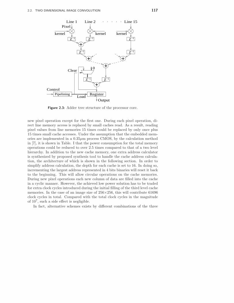
2.2. TWO DIMENSIONAL IMAGE CONVOLUTION 117
−1Z −1Z
−1Z
−1Z −1Z
−1Z
−1Z
Line 1 Line 2 Line 15
0
RegisterLoad
Clear
Pipelining
kernel kernel kernel
Control
Output
Pixel
Figure 2.3: Adder tree structure of the processor core.
new pixel operation except for the first one. During each pixel operation, di-rect line memory access is replaced by small caches read. As a result, readingpixel values from line memories 15 times could be replaced by only once plus15 times small cache accesses. Under the assumption that the embedded mem-ories are implemented in a 0.35µm process CMOS, by the calculation methodin [7], it is shown in Table. I that the power consumption for the total memoryoperations could be reduced to over 2.5 times compared to that of a two levelhierarchy. In addition to the new cache memory, one extra address calculatoris synthesized by proposed synthesis tool to handle the cache address calcula-tion, the architecture of which is shown in the following section. In order tosimplify address calculation, the depth for each cache is set to 16. In doing so,incrementing the largest address represented in 4 bits binaries will reset it backto the beginning. This will allow circular operations on the cache memories.During new pixel operations each new column of data are filled into the cachein a cyclic manner. However, the achieved low power solution has to be tradedfor extra clock cycles introduced during the initial filling of the third level cachememories. In the case of an image size of 256×256, this will contribute 61696clock cycles in total. Compared with the total clock cycles in the magnitudeof 107, such a side effect is negligible.
In fact, alternative schemes exists by different combinations of the three

118CHAPTER 2. CONTROLLER SYNTHESIS IN IMAGE CONVOLUTION HARDWARE
ACCELERATOR DESIGN
Select, EOB
Signals
+1
Control
Logic
Address Branch Address
Status
D
Control
Figure 2.4: Controller Architecture with incremental circuitry.
memories in the hierarchy. All these possible solutions differ substantially inmemory accesses. In Table. I, different memory scheme is shown where M0,C0, C1 denotes off-chip memory, line memories and smaller caches respectively.Although the number of data provided to the datapath remains the same for allfour schemes, the access counts to the large off-chip memories varies. For thetwo and three level hierarchy structures, the counts to the large memory M0 arereduced by nearly 225 times compared to that of the one level solution. Betweenscheme B and D, the least access counts to both external memories and linememories are identified in three level memory structure, but this is achievedat the cost of extra clock cycles introduced during each pixel operation. Thus,trade off should be made when different implementation techniques are used.For the FPGAs where power consumption is considered less significant, twolevel hierarchies prevails due to its lower clock cycle counts. While for ASICsolutions, three level hierarchy is more preferable for it results in reasonablepower reduction.
In addition to memory schemes, a pipelined adder tree is implemented onfour processor cores to fulfil the sustained calculation capacity. Four cores havebeen chosen to be able to perform several convolutions in parallel. Each corecontains 15 multipliers with adjoining RAMs filled with the kernel function.During each clock cycle, one column of data comprising 15 pixel values areread to the corresponding multipliers. The multiplication are performed inparallel and the products are summed in the subsequent adder tree. Combinedwith memory hierarchy, a very high sustained calculation capacity is obtained.

2.3. CONTROLLER SYNTHESIS 119
2.3 Controller synthesis
The processor cores require a very simple controller with only 2 control signals.However, the line memories and caches, plus RAMs accommodating kernelfunction values require extensive address calculations and loop control. In or-der to reduce the effort of the controller design, a synthesis tool is modifiedbased on [1] to support synthesis process from C-like control algorithm speci-fication to RTL controller module in VHDL format. The modified tool takesin a behavioral description of the datapath architecture defining the availableset of micro-operations, and a microprogram written in C-like input syntaxthat contains the algorithm with additional declarations such as memories.As an output a complete controller with module descriptions and interconnec-tion specifications is generated. Since architecture extensions to basic FSMcould result in optimized controllers in specific application, a range of con-troller architectures are supported and can be accessed through architectureoption specification before the synthesis starts. For the current image pro-cessor, a controller architecture with incremental circuitry is implemented, asshown in figure 2.4. In this architecture, the branch address calculation withinthe same block of code, composed of only sequential statements, is performedby the hardware incrementer. At the end of a block a non-incremental branchaddress is calculated by the control logic and a select branch signal is set. Thisarchitecture is particularly suitable for algorithms that have long stretches ofsequential statements, i.e. the next state generation logic in the basic FSMarchitecture can be replaced by an incrementer and MUX. With the tool, morecomplicated architectures can be implemented freely based on user require-ments and algorithm structures since it is a fully automated synthesis process.
In addition to the control structure, address processing units (APU) are alsosynthesized by the tool to perform address calculation. Due to the considerabledata flow in calculating the memory addresses, APUs are usually implementedseparately from controllers to reduce control logic. Declared in the micropro-gram, like variables in C, APUs are implemented in a common structure asshown in figure 2.5. To map the address calculations in the microprogram intohardware, constant value assignments to the APUs are implemented as one ofthe MUX constants. Additions and subtractions are performed in the adderand the results are stored in one of the register banks on either sides. Param-eters such as image size is provided through the external input. To facilitatesimple calculation descriptions in a microprogram, several sets of micro opera-tions are predefined by the synthesis tool so that the user of the microprogramcould use calculation functions like ”++” and ”--” with no knowledge of theimplementation details. This will simplify the microprogram substantially inan address calculation intensive tasks.

120CHAPTER 2. CONTROLLER SYNTHESIS IN IMAGE CONVOLUTION HARDWARE
ACCELERATOR DESIGN
MUX
ADD/SUB
MUX
MUX
External
Sign
Constants
Memory Address
REGBANKREGBANK
Figure 2.5: The address processing unit used in image convolution unit.
In the future, system level modelling language like SystemC is within specialinterest for its ability to specify both algorithm and hardware. With thissupport, future designs could go up further to the system level to enable morecomplicated system design and early verification.
2.4 Results
The control logic is generated in the format of espresso [8]–a PLA design for-mat supported by Synopsys design compiler. Other formats are also likely inthe future since the information stored in the database are truth tables andcould be easily modified for other formats. The associated controller archi-tecture as well as the datapath are implemented in VHDL. The whole systemhas been prototyped on Xilinx VirtexE 1156G FPGAs. Extra parts dealingwith communication with PCs is developed to enable image transfer betweenPC and FPGAs. The whole design works under 20Mhz with a total equivalentgate count of nearly 800000. Matlab is used as an interface for both handlingthe communication on the PC side and results comparison with built-in filterfunctions. The image data are 8 bits unsigned values while the kernel functionsare signed. The results are 24 bits signed values in the form of double preci-sion matrix. The word length is only implemented for comparison with Matlabresults. In real applications, scaling or rounding scheme can be used to reducethe output bits. To demonstrate the functionality, an edge detection operatorMexican hat is chosen to detect image edges in figure 2.6. Convolution resultsfrom different kernel size are given together with their zero crossings. Its dis-
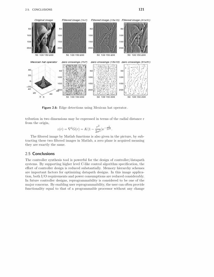
2.5. CONCLUSIONS 121
Figure 2.6: Edge detections using Mexican hat operator.
tribution in two dimensions may be expressed in terms of the radial distance rfrom the origin,
z(r) = ∇2G(r) = K(1 − r2
2σ2)e−
r2
2σ2 .
The filtered image by Matlab functions is also given in the picture, by sub-tracting these two filtered images in Matlab, a zero plane is acquired meaningthey are exactly the same.
2.5 Conclusions
The controller synthesis tool is powerful for the design of controller/datapathsystems. By supporting higher level C-like control algorithm specification, theeffort of controller design is reduced substantially. Memory hierarchy schemesare important factors for optimizing datapath designs. In this image applica-tion, both I/O requirements and power consumptions are reduced considerably.In future controller designs, reprogrammability is considered to be one of themajor concerns. By enabling user reprogrammability, the user can often providefunctionality equal to that of a programmable processor without any change

122CHAPTER 2. CONTROLLER SYNTHESIS IN IMAGE CONVOLUTION HARDWARE
ACCELERATOR DESIGN
of the circuits. In recent years, this has already become a hot topic amongnetworking and wireless communication system designs [9]. But it should berealized that level of programmability be taken as a trade off between perfor-mance and flexibility in the design space [10].

Bibliography
[1] V. Owall, “Synthesis of controllers from a range of controller architec-tures,” Ph.D. dissertation, Lund University, Lund, 1994.
[2] K. karadayi and Y. Kim, “Imaging with texas instruments TMS320C64x,”Texas Instruments White paper, Tech. Rep., December 2001.
[3] E. Jamro and K. Wiatr, “FPGA implementation of addition as a part ofthe convolution,” in Proc. IEEE Euromicro Symposium on Digital SystemsDesign, Warszawa, Poland, September 2001.
[4] ——, “Implementation of image data convolutions operations in FPGA re-configurable structures for real-time vision systems,” in Proc. IEEE Inter-national Conference on Information Technology: Coding and Computing,Nevada, USA, 2000, pp. 152–157.
[5] D. Bilsby, R. Walke, and R. Smith, “Comparison of a programmable DSPand an FPGA for real-time multiscale convolution,” IEE Colloquium onHigh Performance Architectures for Real-Time Image Processing, pp. 4/1–4/6, February 1998.
[6] V. Owall, M. Torkelson, and P. Egelberg, “A custom image convolutiondsp with a sustained calculation capacity of > 1 GMAC/s and low I/Obandwidth,” Springer Journal of VLSI Signal Processing Systems for Sig-nal Image and Video Technology, vol. 23, pp. 335–350, 1999.
[7] F. Catthoor, S. Wuytack, and E. D. Greef, Custom memory managementmethodology. Kluwer Academic Publishers, 1998.
123

124 BIBLIOGRAPHY
[8] R. Rudell, “ESPRESSO - boolean minimization program,” University ofCalifornia at Berkeley, Tech. Rep., December 1985.
[9] K. Keutzer, “Bright future for programmable processors,” IEEE Designand test of Computers, vol. 18, pp. 7–8, November-December 2001.
[10] N. Bang and R. W. Brodersen, “Architectural evaluation of flexible digitalsignal processing for wireless receivers,” in Proc. Thirty-Fourth AsilomarConference on Signals, Systems and Computers, California, USA, October2000, pp. 78–83.