micronas vct 38xxa/b video/controller/teletext …diagramasde.com/diagramas/otros/vct38xxa-b.pdfvct...
TRANSCRIPT

VCT 38xxA/BVideo/Controller/Teletext IC Family
Edition Jan. 8, 20026251-518-1PD
PRELIMINARY DATA SHEET
MICRONAS
MICRONAS

VCT 38xxA/B PRELIMINARY DATA SHEET
2 Micronas
Contents
Page Section Title
7 1. Introduction8 1.1. Features8 1.1.1. Video Features8 1.1.2. Microcontroller Features8 1.1.3. OSD Features8 1.1.4. Teletext Features8 1.1.5. Audio Features8 1.1.6. General Features
9 1.2. Chip Architecture
10 1.3. System Application
11 2. Video Processing11 2.1. Introduction
11 2.2. Video Front-end11 2.2.1. Input Selector11 2.2.2. Clamping11 2.2.3. Automatic Gain Control11 2.2.4. Analog-to-Digital Converters12 2.2.5. Digitally Controlled Clock Oscillator12 2.2.6. Analog Video Output
12 2.3. Adaptive Comb Filter
13 2.4. Color Decoder13 2.4.1. IF-Compensation14 2.4.2. Demodulator14 2.4.3. Chrominance Filter14 2.4.4. Burst Detection / Saturation Control14 2.4.5. Color Killer Operation15 2.4.6. Automatic Standard Recognition15 2.4.7. PAL Compensation/1-H Comb Filter16 2.4.8. Luminance Notch Filter16 2.4.9. Skew Filtering
16 2.5. Horizontal Scaler
17 2.6. Black-line Detector
17 2.7. Test Pattern Generator
17 2.8. Video Sync Processing
18 2.9. Display Processing18 2.9.1. Luma Contrast Adjustment18 2.9.2. Black-Level Expander19 2.9.3. Dynamic Peaking20 2.9.4. Digital Brightness Adjustment20 2.9.5. Soft Limiter20 2.9.6. Chroma Interpolation20 2.9.7. Chroma Transient Improvement21 2.9.8. Inverse Matrix21 2.9.9. RGB Processing21 2.9.10. OSD Color Look-up Table21 2.9.11. Picture Frame Generator22 2.9.12. Priority Decoder22 2.9.13. Scan Velocity Modulation22 2.9.14. Display Phase Shifter
24 2.10. Video Back-end24 2.10.1. CRT Measurement and Control25 2.10.2. SCART Output Signal26 2.10.3. Average Beam Current Limiter26 2.10.4. Analog RGB Insertion26 2.10.5. Fast-Blank Monitor

Contents, continued
Page Section Title
PRELIMINARY DATA SHEET VCT 38xxA/B
Micronas 3
28 2.11. Synchronization and Deflection28 2.11.1. Deflection Processing28 2.11.2. Angle and Bow Correction28 2.11.3. Horizontal Phase Adjustment29 2.11.4. Vertical and East/West Deflection29 2.11.5. EHT Compensation30 2.11.6. Protection Circuitry
30 2.12. Reset Function
30 2.13. Standby and Power-On
31 2.14. I2C Bus Slave Interface31 2.14.1. Control and Status Registers44 2.14.1.1. Scaler Adjustment46 2.14.1.2. Calculation of Vertical and East-West Deflection Coefficients
48 3. Text and OSD Processing48 3.1. Introduction
48 3.2. SRAM Interface
48 3.3. Text Controller
50 3.4. Teletext Acquisition
50 3.5. Teletext Page Management50 3.5.1. Memory Manager51 3.5.2. Memory Organization51 3.5.3. Page Table53 3.5.4. Ghost Row Organization54 3.5.5. Subpage Manager
55 3.6. WST Display Controller
56 3.7. Display Memory
58 3.8. Character Generator59 3.8.1. Character Code Mapping60 3.8.2. Character Font ROM61 3.8.3. Latin Font Mapping62 3.8.4. Cyrillic Font Mapping63 3.8.5. Arabic Font Mapping64 3.8.6. Closed Caption Font (on VCT 38xxB only!)65 3.8.7. Character Font Structure
66 3.9. National Character Mapping
68 3.10. Four-Color Mode
69 3.11. OSD Layer
70 3.12. Command Language
78 3.13. I/O Register
85 3.14. I2C-Bus Slave Interface85 3.14.1. Subaddressing86 3.14.1.1. CPU Subaddressing86 3.14.1.2. DRAM Subaddressing86 3.14.1.3. Command Subaddressing87 3.14.1.4. Data Subaddressing87 3.14.1.5. Hardware Identification

VCT 38xxA/B PRELIMINARY DATA SHEET
4 Micronas
Contents, continued
Page Section Title
88 4. Audio Processing88 4.1. Introduction
88 4.2. Input Select
88 4.3. Volume Control
88 4.4. I2C-Bus Slave Interface
89 5. TV Controller89 5.1. Introduction
89 5.2. CPU89 5.2.1. CPU Slow Mode
90 5.3. RAM and ROM90 5.3.1. Address Map90 5.3.2. Bootloader
91 5.4. Control Register
93 5.5. Standby Registers
94 5.6. Test Registers
95 5.7. Reset Logic95 5.7.1. Alarm Function95 5.7.2. Software Reset95 5.7.2.1. From Standby into Normal Mode95 5.7.2.2. From Normal into Standby Mode96 5.7.3. Internal Reset Sources96 5.7.3.1. Supply Supervision96 5.7.3.2. Clock Supervision97 5.7.3.3. Watchdog98 5.7.4. External Reset Sources98 5.7.5. Summary of Module Reset States98 5.7.6. Reset Registers
99 5.8. Memory Banking99 5.8.1. Banking Register
101 5.9. DMA Interface103 5.9.1. DMA Registers
104 5.10. Interrupt Controller104 5.10.1. Features104 5.10.2. General104 5.10.3. Initialization104 5.10.4. Operation104 5.10.5. Inactivation106 5.10.6. Precautions107 5.10.7. Interrupt Registers109 5.10.8. Interrupt Assignment109 5.10.8.1. Interrupt Multiplexer111 5.10.9. Port Interrupt Module113 5.10.10. Interrupt Timing
114 5.11. Memory Patch Module114 5.11.1. Features114 5.11.2. General114 5.11.3. Initialization115 5.11.4. Patch Operation115 5.11.5. Patch Registers
116 5.12. I2C-Bus Master Interface118 5.12.1. I2C Bus Master Interface Registers
120 5.13. Timer T0 and T1120 5.13.1. Features120 5.13.2. Operation121 5.13.3. Timer Registers

Contents, continued
Page Section Title
PRELIMINARY DATA SHEET VCT 38xxA/B
Micronas 5
122 5.14. Capture Compare Module (CAPCOM)122 5.14.1. Features123 5.14.2. Initialization123 5.14.3. Operation of CCC123 5.14.3.1. Operation of Subunit123 5.14.3.2. Compare and Output Action124 5.14.3.3. Capture and Input Action124 5.14.3.4. Interrupts124 5.14.4. Inactivation125 5.14.5. CAPCOM Registers
127 5.15. Pulse Width Modulator127 5.15.1. Features127 5.15.2. General127 5.15.3. Initialization127 5.15.4. Operation127 5.15.5. PWM Registers
128 5.16. Tuning Voltage Pulse Width Modulator128 5.16.1. Features128 5.16.2. General129 5.16.3. Initialization129 5.16.4. Operation129 5.16.5. TVPWM Registers
130 5.17. A/D Converter (ADC)130 5.17.1. Features131 5.17.2. Operation131 5.17.3. Measurement Errors131 5.17.4. Comparator132 5.17.5. ADC Registers
133 5.18. Closed Caption Module (CC)133 5.18.1. Features134 5.18.2. Operation134 5.18.2.1. Lowpass filter134 5.18.2.2. Input timing134 5.18.2.3. Threshold adaption134 5.18.2.4. Bitslicing134 5.18.2.5. Timing recovery134 5.18.2.6. Shift register134 5.18.2.7. Controlling134 5.18.2.8. Formatter135 5.18.3. CCM Registers
137 5.19. Ports137 5.19.1. Port Assignment138 5.19.2. Universal Ports P1 to P3138 5.19.2.1. Features139 5.19.2.2. Universal Port Mode139 5.19.3. Universal Port Registers140 5.19.4. I2C Ports P40 and P41140 5.19.4.1. Features141 5.19.5. Audio Ports P42 to P46141 5.19.5.1. Features142 5.19.6. CLK20 Output Port142 5.19.6.1. Features
143 5.20. I/O Register Cross Reference

VCT 38xxA/B PRELIMINARY DATA SHEET
6 Micronas
Contents, continued
Page Section Title
147 6. Specifications147 6.1. Outline Dimensions
148 6.2. Pin Connections and Short Descriptions
152 6.3. Pin Descriptions for PSDIP64 package
154 6.4. Pin Descriptions for PMQFP128 package
155 6.5. Pin Configuration
157 6.6. Pin Circuits
160 6.7. Electrical Characteristics160 6.7.1. Absolute Maximum Ratings160 6.7.2. Recommended Operating Conditions160 6.7.2.1. General Recommendations161 6.7.2.2. Analog Input and Output Recommendations162 6.7.2.3. Recommended Crystal Characteristics163 6.7.3. Characteristics163 6.7.3.1. General Characteristics163 6.7.3.2. Test Input164 6.7.3.3. Reset Input/Output164 6.7.3.4. I2C Bus Interface165 6.7.3.5. 20-MHz Clock Output165 6.7.3.6. Analog Video Output165 6.7.3.7. A/D Converter Reference166 6.7.3.8. Analog Video Front-End and A/D Converters168 6.7.3.9. Analog RGB and FB Inputs169 6.7.3.10. Horizontal Flyback Input169 6.7.3.11. Horizontal Drive Output169 6.7.3.12. Vertical Safety Input169 6.7.3.13. Vertical Protection Input170 6.7.3.14. Vertical and East/West D/A Converter Output170 6.7.3.15. Interlace Output170 6.7.3.16. Sense A/D Converter Input170 6.7.3.17. Range Switch Output171 6.7.3.18. D/A Converter Reference171 6.7.3.19. Analog RGB Outputs, D/A Converters174 6.7.3.20. Scan Velocity Modulation Output174 6.7.3.21. Analog Audio Inputs and Outputs175 6.7.3.22. ADC Input Port175 6.7.3.23. Universal Port & Memory Interface 176 6.7.3.24. Memory Interface
177 7. Application
180 8. Glossary of Abbreviations
180 9. References
182 10. Data Sheet History
PRELIMINARY DATA SHEET VCT 38xxA/B
Micronas 7
Video/Controller/Teletext IC Family
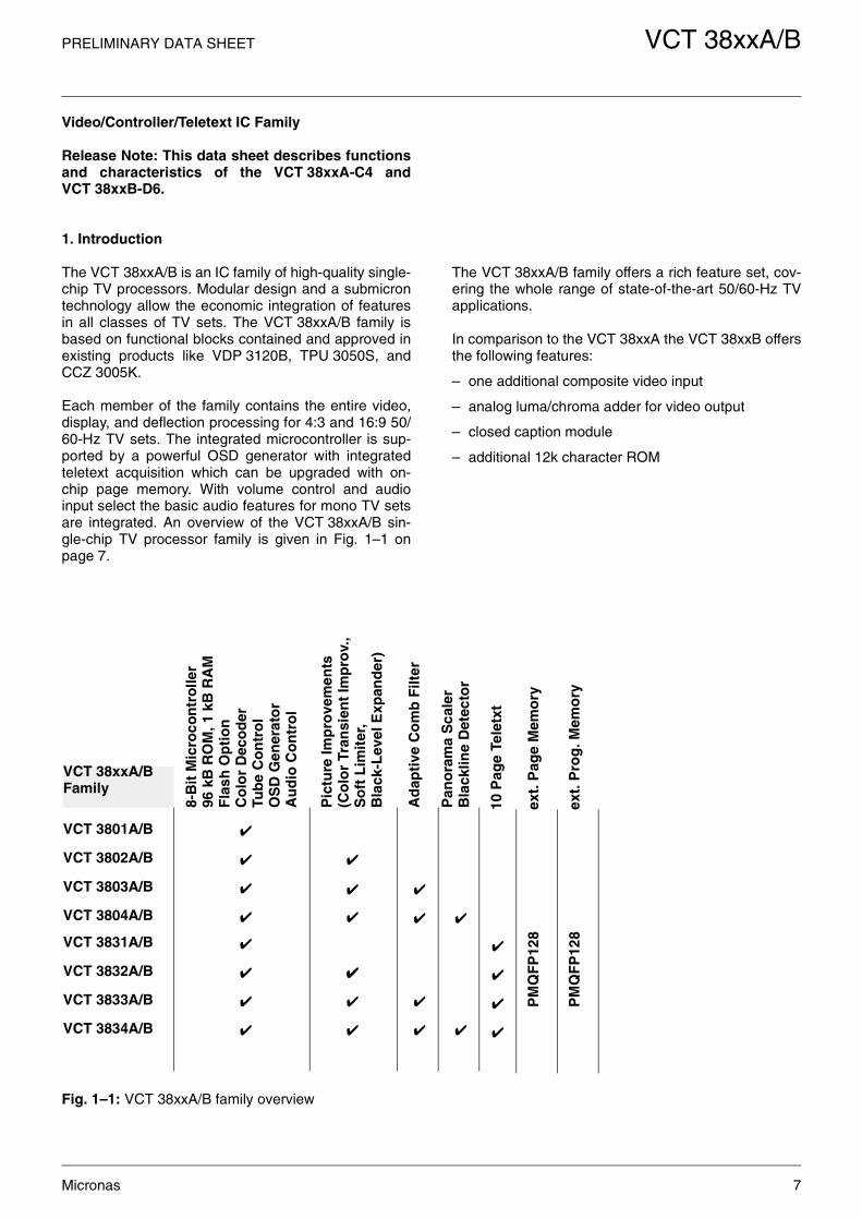
Release Note: This data sheet describes functionsand characteristics of the VCT 38xxA-C4 andVCT 38xxB-D6.
1. Introduction
The VCT 38xxA/B is an IC family of high-quality single-chip TV processors. Modular design and a submicrontechnology allow the economic integration of featuresin all classes of TV sets. The VCT 38xxA/B family isbased on functional blocks contained and approved inexisting products like VDP 3120B, TPU 3050S, andCCZ 3005K.
Each member of the family contains the entire video,display, and deflection processing for 4:3 and 16:9 50/60-Hz TV sets. The integrated microcontroller is sup-ported by a powerful OSD generator with integratedteletext acquisition which can be upgraded with on-chip page memory. With volume control and audioinput select the basic audio features for mono TV setsare integrated. An overview of the VCT 38xxA/B sin-gle-chip TV processor family is given in Fig. 1–1 onpage 7.
The VCT 38xxA/B family offers a rich feature set, cov-ering the whole range of state-of-the-art 50/60-Hz TVapplications.
In comparison to the VCT 38xxA the VCT 38xxB offersthe following features:
– one additional composite video input
– analog luma/chroma adder for video output
– closed caption module
– additional 12k character ROM
Fig. 1–1: VCT 38xxA/B family overview
Ad
apti
ve C
om
b F
ilter
Pan
ora
ma
Sca
ler
Bla
cklin
e D
etec
tor
Pic
ture
Imp
rove
men
ts(C
olo
r Tr
ansi
ent
Imp
rov.
,S
oft
Lim
iter
,B
lack
-Lev
el E
xpan
der
)
10 P
age
Tele
txt
VCT 38xxA/BFamily
VCT 3801A/B
ext.
Pro
g. M
emo
ry
8-B
it M
icro
con
tro
ller
96 k
B R
OM
, 1 k
B R
AM
Fla
sh O
pti
on
Co
lor
Dec
od
erTu
be
Co
ntr
ol
OS
D G
ener
ato
rA
ud
io C
on
tro
l
ext.
Pag
e M
emo
ry
VCT 3803A/B
VCT 3804A/B
VCT 3831A/B
VCT 3832A/B
VCT 3833A/B
VCT 3834A/B
PM
QF
P12
8
PM
QF
P12
8
VCT 3802A/B

VCT 38xxA/B PRELIMINARY DATA SHEET
8 Micronas
1.1. Features
1.1.1. Video Features
– four composite video inputs (VCT 38xxA)
– five composite video inputs (VCT 38xxB)
– analog YCrCb input, two S-VHS inputs
– Y/C adder for video output (VCT 38xxB only!)
– composite video monitor
– multistandard color decoder (1 crystal)
– multistandard sync decoder
– black-line detector
– adaptive 2H comb filter Y/C separator
– horizontal scaling (0.25 to 4)
– Panoramavision
– black-level expander
– dynamic peaking
– soft limiter (gamma correction)
– color transient improvement
– programmable RGB matrix
– analog RGB/Fastblank input
– half-contrast switch
– picture frame generator
– scan velocity modulation output
– high-performance H/V deflection
– angle and bow correction
– separate ADC for tube measurements
– EHT compensation
1.1.2. Microcontroller Features
– 8-bit, 10-MHz CPU (65C02)
– 96 kB program ROM on chip
– 1 kB program RAM on chip
– memory banking
– 16-input, 16-level interrupt controller
– patch module for 10 ROM locations
– two 16-bit reloadable timers
– capture compare module
– watchdog timer
– 14-bit PWM for voltage synthesis
– four 8-bit PWMs
– 10-bit ADC with 15:1 input MUX
– I2C bus master interface
– 24 programmable I/O ports
– closed caption module (VCT 38xxB only!)
1.1.3. OSD Features
– 3 kB OSD RAM on chip
– WST level 1.5 compliant
– WST level 2 parallel attributes
– 32 foreground/background colors
– programmable color look-up table
– 1024 mask programmable characters (VCT 38xxA)
– 2000 mask programmable characters (VCT 38xxB)
– 24 national languages (Latin, Cyrillic, Greek, Arabic, Farsi, Hebrew)
– character matrix 8x8, 8x10, 8x13, 10x8, 10x10, 10x13
– vertical soft scroll
– 4-color mode for user font
1.1.4. Teletext Features
– four programmable video inputs (VCT 38xxA)
– five programmable video inputs (VCT 38xxB)
– acquisition is independent from display part
– adaptive data slicer
– signal quality detection
– WST, PDC, VPS, and WSS acquisition
– high-level command language
– EPG, FLOF, and TOP support
– 10 pages memory on chip
– up to 500 pages with external SRAM
1.1.5. Audio Features
– three mono inputs
– two mono outputs
– programmable channel select
– volume control for one mono channel
1.1.6. General Features
– submicron CMOS technology
– low-power standby mode
– single 20.25-MHz crystal
– 64-pin PSDIP package
– 128-pin PMQFP package
– emulator chip for software development

PRELIMINARY DATA SHEET VCT 38xxA/B
Micronas 9
1.2. Chip Architecture
Fig. 1–2: Block diagram of the VCT 38xxA/B (shaded blocks are optional)
The block diagram does not show the additional features of VCT 38xxB.
Video Front-end
Comb Filter
Color Decoder
Display Processor Video
Back-endPanorama
Scaler
4 3
4
12
31
2I2C Master
3 kBOSD
96 kB CPU ROM
TPU DMA CPU
24 IO Ports
Watchdog
2 CapCom
2 Timer
15:1 Mux10-bit ADC
8-bit PWM
Audio 3
2
Clock Oscillator
1 kB CPU RAM
XTAL1
XTAL2
VIN
AIN
Pxy
ADB, DB, CB
RGBOUT
RGBIN
VE
RT
PR
OT
HF
LB
SE
NS
E
I2C
XR
EF
HO
UT
VR
D
VR
T
SG
ND
Color, PrioMSyncI2C
VSUPAB
VS
UP
P1
GN
DP
1
Reset Logic
RESQ
VS
UP
S
TEST
GNDAB
VS
UP
AF
VS
UP
D
GN
DA
F
GN
DD
RS
W
2
GN
DM
EW
8
14-bit PWM
2 2
3CIN SVM
Vid
eo
GN
DS
CLK20
RDY
BE
24 kB
VCT 38xxA/B
AOUT
VSync
VOUT
24 kB ROM
3 kB OSD RAM
Pict.Improv
16 kB Text RAM

VCT 38xxA/B PRELIMINARY DATA SHEET
10 Micronas
1.3. System Application
Fig. 1–3: Single-chip TV with VCT 38xxA/B
VCT 38xxA/B
20.25MHz
512kSRAM
CVBS1
CVBS2
Cr
optional memory extension
Y
Cb
C
Loudspeaker
Tuner/SCART/FrontAV
An
alo
g V
ideo
Analog Audio
CRT
Analog RGBSCART
512kROM/
FLASH
CECEOE2WE2
ADB
DB
OE1 WE1
Y

PRELIMINARY DATA SHEET VCT 38xxA/B
Micronas 11
2. Video Processing
2.1. Introduction
The VCT 38xxA/B includes complete video, display,and deflection processing. In the following sections thevideo processing part of the VCT 38xxA/B will benamed VDP for short.
All processing is done digitally, the video front-end andvideo back-end are interfacing to the analog world.Most functions of the VDP can be controlled by soft-ware via I2C bus slave interface (see Section 2.14. onpage 31).
2.2. Video Front-end
This block provides the analog interfaces to all videoinputs and mainly carries out analog-to-digital conver-sion for the following digital video processing. A blockdiagram is given in Fig. 2–1.
Most of the functional blocks in the front-end are digi-tally controlled (clamping, AGC, and clock-DCO). Thecontrol loops are closed by the Fast Processor (‘FP’)embedded in the video decoder.
2.2.1. Input Selector
Up to eight analog inputs can be connected. Fourinputs (five in case of VCT 38xxB) are for input of com-posite video or S-VHS luma signal. These inputs areclamped to the sync back porch and are amplified by avariable gain amplifier. Two chroma inputs can beused for connection of S-VHS carrier-chrominance sig-nal. These inputs are internally biased and have afixed gain amplifier. For analog YCrCb signals (e.g.from DVD players) one of the selected luminanceinputs is used together with CBIN and CRIN inputs.
2.2.2. Clamping
The composite video input signals are AC-coupled tothe IC. The clamping voltage is stored on the couplingcapacitors and is generated by digitally controlled cur-rent sources. The clamping level is the back porch ofthe video signal. S-VHS chrominance is also AC-cou-pled. The input pin is internally biased to the center ofthe ADC input range. The chrominance inputs forYCrCb need to be AC-coupled by 220 nF clampingcapacitors. It is strongly recommended to use 5-MHzanti-alias low-pass filters on each input. Each channelis sampled at 10.125 MHz with a resolution of 8 bit anda clamping level of 128.
2.2.3. Automatic Gain Control
A digitally working automatic gain control adjusts themagnitude of the selected baseband by +6/–4.5 dB in64 logarithmic steps to the optimal range of the ADC.The gain of the video input stage including the ADC is213 steps/V with the AGC set to 0 dB. The gain of thechrominance path in the YCrCb mode is fix andadapted to a nominal amplitude of 0.7 Vpp. However, ifan overflow of the ADC occurs an extended signalrange from 1 Vpp can be selected.
2.2.4. Analog-to-Digital Converters
Two ADCs are provided to digitize the input signals.Each converter runs with 20.25 MHz and has 8 bit res-olution. An integrated bandgap circuit generates therequired reference voltages for the converters.
Fig. 2–1: Video front-end
VIN2
VIN3
VIN4
CIN1
VIN1
Bias ADC
ADC
Gain
Clamp
Inpu
t
FrequencyReferenceGeneration
DVCO±150ppm
AGC+6/–4.5 dB
digital CVBS or Luma
digital Chroma
System Clocks
20.25 MHz
CVBS/Y
CVBS/Y
CVBS/Y
CVBS/Y
Chroma
Mux
CIN2Chroma
ClampCBIN
Chroma
CRIN
mux
VOUTCVBS/Y
3
VIN5CVBS/Y
+

VCT 38xxA/B PRELIMINARY DATA SHEET
12 Micronas
2.2.5. Digitally Controlled Clock Oscillator
The clock generation is also a part of the analog front-end. The crystal oscillator is controlled digitally by thecontrol processor. The clock frequency can beadjusted within ±150 ppm.
2.2.6. Analog Video Output
The input signal of the Luma ADC is available at theanalog video output pin. The signal at this pin must bebuffered by a source follower. The output voltage is2 V, thus the signal can be used to drive a 75-Ω line.The magnitude is adjusted with an AGC in 8 stepstogether with the main AGC.
In case of VCT 38xxB it is possible to enable a Y/C-adder. The analog sum of the selected luma andchroma input signals is available at the video outputpin. This allows recording of S-VHS input signals viavideo output.
2.3. Adaptive Comb Filter
The adaptive comb filter is used for high-quality lumi-nance/chrominance separation for PAL or NTSC sig-nals. The comb filter improves the luminance resolu-tion (bandwidth) and reduces interferences likecross-luminance and cross-color artifacts. The adap-tive algorithm can eliminate most of the mentionederrors without introducing new artifacts or noise.
A block diagram of the comb filter is shown in Fig. 2–2.The filter uses two line delays to process the informa-tion of three adjacent video lines. To have a fixedphase relationship of the color subcarrier in the threechannels, the system clock (20.25 MHz) is locked to
the color subcarrier. This allows the processing of allcolor standards and substandards using a single crys-tal frequency.
The CVBS signal in the three channels is filtered at thesubcarrier frequency by a set of bandpass/notch fil-ters. The output of the three channels is used by theadaption logic to select the weighting that is used toreconstruct the luminance/chrominance signal fromthe 4 bandpass/notch filter signals.The comb filteruses the middle line as reference, therefore, the combfilter delay is one line. If the comb filter is switched off,the delay lines are used to pass the luma/ chroma sig-nals from the A/D converters to the luma/ chroma out-puts. Thus, the comb filter delay is always one line.
Various parameters of the comb filter are adjustable,hence giving to the user the ability to adjust his owndesired picture quality.
Two parameters (KY, KC) set the global gain of lumaand chroma comb separately; these values directlyweigh the adaption algorithm output. In this way, it ispossible to obtain a luma/chroma separation rangingfrom standard notch/bandpass to full comb decoding.
The parameter KB allows to choose between the twoproposed comb booster modes. This so-called featurewidely improves vertical high-to-low frequency transi-tions areas, the typical example being a multiburst toDC change. For KB=0, this improvement is kept mod-erate, whereas, in case of KB=1, it is maximum, butthe risk to increase the “hanging dots” amount forsome given color transitions is higher.
Using the default setting, the comb filter has separateluma and chroma decision algorithms; however, it ispossible to switch the chroma comb factor to the cur-rent luma adaption output by setting CC to 1.
Fig. 2–2: Block diagram of the adaptive comb filter (PAL mode)
1H Delay Line
1H Delay Line
CVBS Input
Chroma Input
BandpassFilter
BandpassFilter
Bandpass/NotchFilter
Lum
a / C
hrom
a M
ixer
sA
dapt
ion
Logi
c
Luma Output
Chroma Output

PRELIMINARY DATA SHEET VCT 38xxA/B
Micronas 13
Another interesting feature is the programmable limita-tion of the luma comb amount; proper limitation, asso-ciated to adequate luma peaking, gives rise to anenhanced 2-D resolution homogeneity. This limitationis set by the parameter CLIM, ranging from 0 (no limi-tation) to 31 (max. limitation).
The DAA parameter (1:off, 0:on) is used to disable/enable a very efficient built-in “rain effect” suppressor;many comb filters show this side effect which givessome vertical correlation to a 2-D uniform randomarea, due to the vertical filtering. This unnatural-look-ing phenomenon is mostly visible on tuner images,since they are always corrupted by some noise; andthis looks like rain.
2.4. Color Decoder
A block diagram of the color decoder is shown in Fig.2–4. The luma as well as the chroma processing, isshown here. The color decoder provides also somespecial modes, e.g. wide band chroma format which isintended for S-VHS wide bandwidth chroma.
If the adaptive comb filter is used for luma chroma sep-aration, the color decoder uses the S-VHS mode pro-cessing. The output of the color decoder is YCrCb in a4:2:2 format.
2.4.1. IF-Compensation
With off-air or mistuned reception, any attenuation athigher frequencies or asymmetry around the color sub-carrier is compensated. Four different settings of theIF-compensation are possible:
– flat (no compensation)
– 6 dB/octave
– 12 dB/octave
– 10 dB/MHz
The last setting gives a very large boost to high fre-quencies. It is provided for SECAM signals that aredecoded using a SAW filter specified originally for thePAL standard.
Fig. 2–3: Frequency response of chroma IF-compensation
Fig. 2–4: Color decoder
ColorPLL/ColorACC
1 H Delay
MU
XM
UX
CrossSwitch
NotchFilter
Luma / CVBS Luma
Chroma
MixerLow-pass FilterPhase/FreqDemodulator
ACC
Chroma
IF Compensation
DC-Reject

VCT 38xxA/B PRELIMINARY DATA SHEET
14 Micronas
2.4.2. Demodulator
The subcarrier frequency in the demodulator is gener-ated by direct digital synthesis; therefore, substan-dards such as PAL 3.58 or NTSC 4.43 can also bedemodulated.
2.4.3. Chrominance Filter
The demodulation is followed by a low-pass filter forthe color difference signals for PAL/NTSC. SECAMrequires a modified low-pass function with bell-filtercharacteristic. At the output of the low-pass filter, allluma information is eliminated.
The low-pass filters are calculated in time multiplex forthe two color signals. Three bandwidth settings (nar-row, normal, broad) are available for each standard.For PAL/NTSC, a wide band chroma filter can beselected. This filter is intended for high bandwidthchroma signals, e.g. a non-standard wide bandwidthS-VHS signal.
Fig. 2–5: Frequency response of chroma filters
2.4.4. Burst Detection / Saturation Control
In the PAL/NTSC-system the burst is the reference forthe color signal. The phase and magnitude outputs ofthe color demodulator are gated with the color key andused for controlling the phase-locked-loop (APC) of thedemodulator and the automatic color control (ACC) inPAL/NTSC.
The ACC has a control range of +30...−6 dB.
Color saturation can be selected once for all colorstandards. In PAL/NTSC it is used as reference for theACC. In SECAM the necessary gains are calculatedautomatically.
For SECAM decoding, the frequency of the burst ismeasured. Thus, the current chroma carrier frequencycan be identified and is used to control the SECAMprocessing. The burst measurements also control thecolor killer operation; they are used for automatic stan-dard detection as well.
2.4.5. Color Killer Operation
The color killer uses the burst-phase/burst-frequencymeasurement to identify a PAL/NTSC or SECAM colorsignal. For PAL/NTSC, the color is switched off (killed)as long as the color subcarrier PLL is not locked. ForSECAM, the killer is controlled by the toggle of theburst frequency. The burst amplitude measurement isused to switch-off the color if the burst amplitude isbelow a programmable threshold. Thus, color will bekilled for very noisy signals. The color amplitude killerhas a programmable hysteresis.
PAL/NTSC
SECAM

PRELIMINARY DATA SHEET VCT 38xxA/B
Micronas 15
2.4.6. Automatic Standard Recognition
The burst-frequency measurement is also used forautomatic standard recognition (together with the sta-tus of horizontal and vertical locking) thus allowing acompletely independent search of the line and colorstandard of the input signal. The following standardscan be distinguished:
– PAL B,G,H,I
– PAL M
– PAL N
– PAL 60
– NTSC M
– NTSC 44
– SECAM
For a preselection of allowed standards, the recogni-tion can be enabled/disabled via I2C bus for each stan-dard separately.
If at least one standard is enabled, the VCT 38xxA/Bregularly checks the horizontal and vertical locking ofthe input signal and the state of the color killer. If anerror exists for several adjacent fields a new standardsearch is started. Depending on the measured linenumber and burst frequency, the current standard isselected.
For error handling the recognition algorithm deliversthe following status information:
– search active (busy)
– search terminated, but failed
– found standard is disabled
– vertical standard invalid
– no color found
2.4.7. PAL Compensation/1-H Comb Filter
The color decoder uses one fully integrated delay line.Only active video is stored.
The delay line application depends on the color stan-dard:
– NTSC: 1-H comb filter or color compensation
– PAL: color compensation
– SECAM: crossover switch
In the NTSC compensated mode, (Fig. 2–6c), the colorsignal is averaged for two adjacent lines. Thus,cross-color distortion and chroma noise is reduced. In
the NTSC comb filter mode, (Fig. 2–6d), the delay lineis in the composite signal path, thus allowing reductionof cross-color components, as well as cross-lumi-nance. The loss of vertical resolution in the luminancechannel is compensated by adding the vertical detailsignal with removed color information.
Fig. 2–6: NTSC color decoding options
Fig. 2–7: PAL color decoding options
Fig. 2–8: SECAM color decoding
chroma
Notchfilter8
ChromaProcess.
CVBSY
1 HDelay
8
CVBS
ChromaProcess.
Notchfilter
Y
8
ChromaProcess.
Luma Y
8C Cr b
C Cr b
C Cr b
Notchfilter
1 HDelay
8
ChromaProcess.
CVBS Y
C Cr b
d) comb filter
c) compensated
a) conventional b) S-VHS
Chroma
Notchfilter
1 HDelay
8
ChromaProcess.
CVBS Y
8
ChromaProcess.
LumaY
81 H
Delay
C Cr b
C Cr b
a) conventional
b) S-VHS
MUX
Notchfilter
1 HDelay
8
ChromaProcess.
CVBS Y
C Cr b

VCT 38xxA/B PRELIMINARY DATA SHEET
16 Micronas
2.4.8. Luminance Notch Filter
If a composite video signal is applied, the color infor-mation is suppressed by a programmable notch filter.The position of the filter center frequency depends onthe subcarrier frequency for PAL/NTSC. For SECAM,the notch is directly controlled by the chroma carrierfrequency. This considerably reduces the cross-lumi-nance. The frequency responses for all three systemsare shown in Fig. 2–9.
Fig. 2–9: Frequency responses of the luma notch filter for PAL, NTSC, SECAM
2.4.9. Skew Filtering
The system clock is free-running and not locked to theTV line frequency. Therefore, the ADC sampling pat-tern is not orthogonal. The decoded YCrCb signals areconverted to an orthogonal sampling raster by theskew filters, which are part of the scaler block.
The skew filters allow the application of a group delayto the input signals without introducing waveform orfrequency response distortion.
The amount of phase shift of this filter is controlled bythe horizontal PLL1. The accuracy of the filters is 1/32clocks for luminance and 1/4 clocks for chroma. Thusthe 4:2:2 YCrCb data is in an orthogonal pixel formateven in the case of nonstandard input signals such asVCR.
2.5. Horizontal Scaler
The 4:2:2 YCrCb signal from the color decoder is pro-cessed by the horizontal scaler. The scaler blockallows a linear or nonlinear horizontal scaling of theinput video signal in the range of 0.25 to 4. Nonlinearscaling, also called “Panoramavision”, provides a geo-metrical distortion of the input picture. It is used to fit apicture with 4:3 format on a 16:9 screen by stretchingthe picture geometry at the borders. Also, the inverseeffect can be produced by the scaler. A summary ofscaler modes is given in Table 2–1.
The scaler contains a programmable decimation filter,a 1-line FIFO memory, and a programmable interpola-tion filter. The scaler input filter is also used for pixelskew correction (see Section 2.4.9. on page 16). Thedecimator/interpolator structure allows optimal use ofthe FIFO memory. The controlling of the scaler is doneby the internal Fast Processor.
dB
MHz
10
0 2 4 6 8 10
0
–10
–20
–30
–40
dB
MHz
10
0 2 4 6 8 10
0
–10
–20
–30
–40
PAL/NTSC notch filter
SECAM notch filter
Table 2–1: Scaler modes
Mode Scale Factor
Description
Compression4:3 → 16:9
0.75linear
4:3 source displayed on a 16:9 tube,with side panels
Panorama4:3 →16:9
non-linearcompr
4:3 source displayed on a 16:9 tube,Borders distorted
Zoom4:3 → 4:3
1.33linear
Letterbox source (PAL+) displayed on a 4:3 tube,vertical overscan with cropping of side panels
Panorama4:3 → 4:3
non-linearzoom
Letterbox source (PAL+) displayed on a 4:3 tube,vertical overscan, bor-ders distorted, no crop-ping

PRELIMINARY DATA SHEET VCT 38xxA/B
Micronas 17
2.6. Black-line Detector
This function is available for versions with pan-orama scaler only!
In case of a letterbox format input video, e.g. Cinema-scope, PAL+ etc., black areas at the upper and lowerpart of the picture are visible. It is suitable to remove orreduce these areas by a vertical zoom and/or shiftoperation.
The VCT 38xxA/B supports this feature by a letterboxdetector. For every field the number of black lines atthe upper and lower part of the picture are measuredand stored in the I2C-register BLKLIN. To adjust thepicture amplitude, the CPU reads this register, calcu-lates the vertical scaling coefficient and transfers thenew settings, e.g. vertical sawtooth parameters, hori-zontal scaling coefficient etc., to the scaler and thedeflection circuits.
Letterbox signals containing logos on the left or rightside of the black areas are processed as black lines,while subtitles, inserted in the black areas, are pro-cessed as non-black lines. Therefore, the subtitles arevisible on the screen. To suppress the subtitles, thevertical zoom coefficient is calculated by selecting thelarger number of black lines only. Dark video sceneswith a low contrast level compared to the letterboxarea are indicated by the BLKPIC bit.
2.7. Test Pattern Generator
The YCrCb outputs can be switched to a test modewhere YCrCb data are generated digitally in theVCT 38xxA/B. Test patterns include luma/chromaramps and flat fields.
2.8. Video Sync Processing
Fig. 2–10 shows a block diagram of the front-end syncprocessing. To extract the sync information from thevideo signal, a linear phase low-pass filter eliminatesall noise and video contents above 1 MHz. The sync isseparated by a slicer; the sync phase is measured. Avariable window can be selected to improve the noiseimmunity of the slicer. The phase comparator mea-sures the falling edge of sync, as well as the integratedsync pulse.
The sync phase error is filtered by a phase-locked loopthat is computed by the FP. All timing in the front-endis derived from a counter that is part of this PLL, and itthus counts synchronously to the video signal.
A separate hardware block measures the signal backporch and also allows gathering the maximum/mini-mum of the video signal. This information is processedby the FP and used for gain control and clamping.
For vertical sync separation, the sliced video signal isintegrated. The FP uses the integrator value to derivevertical sync and field information.
The information extracted by the video sync process-ing is multiplexed onto the hardware front sync signal(FSY) and is distributed to the rest of the video pro-cessing system.
The data for the vertical deflection, the sawtooth, andthe East-West correction signal is calculated by theVCT 38xxA/B. The data is buffered in a FIFO andtransferred to the back-end by a single wire interface.
Frequency and phase characteristics of the analogvideo signal are derived from PLL1. The results are fedto the scaler unit for data interpolation and orthogonal-ization and to the clock synthesizer for line-lockedclock generation. Horizontal and vertical syncs arelatched with the line-locked clock.
Fig. 2–10: Sync separation block diagram
phasecomparator
&lowpass
counter
front-endtiming
front synclowpass1 MHz
&sync slicer
horizontalsync
separation
verticalsync
separationFIFO
Sawtooth
videoinput
skewfrontsync
generator
verticalserialdata
vertical
sawtoothE/W
ParabolaCalculation
clamping, colorkey, FIFO_write
PLL1
clamp &signalmeas.
vblankfield
clocksynthesizer
syncsclockH/V syncs

VCT 38xxA/B PRELIMINARY DATA SHEET
18 Micronas
2.9. Display Processing
In the display processing the conversion from digitalYCrCb to analog RGB is carried out. A block diagramis shown in Fig. 2–18 on page 23. In the luminanceprocessing path, contrast and brightness adjustmentsand a variety of features, such as black-level expan-sion, dynamic peaking and soft limiting, are provided.In the chrominance path, the CrCb signals are con-verted to 4:4:4 format and filtered by a color transientimprovement circuit. The YCrCb signals are convertedby a programmable matrix to RGB color space.
The display processor provides separate control set-tings for two pictures, i.e. different coefficients for a‘main’ and a ‘side’ picture.
The digital OSD insertion circuit allows the insertion ofa 5-bit OSD signal. The color space for this signal iscontrolled by a partially programmable color look-uptable (CLUT) and contrast adjustment.
The OSD signals and the display clock are synchro-nized to the horizontal flyback. For the display clock, agate delay phase shifter is used. In the analog back-end, three 10-bit digital-to-analog converters providethe analog output signals.
2.9.1. Luma Contrast Adjustment
The contrast of the luminance signal can be adjustedby multiplication with a 6-bit contrast value. The con-trast value corresponds to a gain factor from 0 to 2,where the value 32 is equivalent to a gain of 1. Thecontrast can be adjusted separately for main pictureand side picture.
2.9.2. Black-Level Expander
The black-level expander enhances the contrast of thepicture. Therefore the luminance signal is modifiedwith an adjustable, non-linear function. Dark areas ofthe picture are changed to black, while bright areasremain unchanged. The advantage of this black-levelexpander is that the black expansion is performed onlyif it will be most noticeable to the viewer.
The black-level expander works adaptively. Dependingon the measured amplitudes ‘Lmin’ and ‘Lmax’ of thelow-pass-filtered luminance and an adjustable coeffi-cient BTLT, a tilt point ‘Lt’ is established by
Lt = Lmin + BTLT (Lmax - Lmin).
Above this value there is no expansion, while all lumi-nance values below this point are expanded accordingto:
Lout = Lin + BAM (Lin - Lt)
A second threshold, Ltr, can be programmed, abovewhich there is no expansion. The characteristics of theblack-level expander are shown in Fig. 2–11 and Fig.2–12.
Fig. 2–11: Characteristics of the black-level expander
The tilt point Lt is a function of the dynamic range ofthe video signal. Thus, the black-level expansion isonly performed when the video signal has a largedynamic range. Otherwise, the expansion to black iszero. This allows the correction of the characteristicsof the picture tube.
Fig. 2–12: Black-level expansiona) luminance inputb) luminance input and output
Lmin
BTLT
BAM
Lt
Ltr
Lmax
Ltr BTHR Lin
Lout
a)
b)
Lmin
Lt
Lmax
Lt

PRELIMINARY DATA SHEET VCT 38xxA/B
Micronas 19
2.9.3. Dynamic Peaking
Especially with decoded composite signals and notchfilter luminance separation, as input signals, it is nec-essary to improve the luminance frequency character-istics. With transparent, high-bandwidth signals, it issometimes desirable to soften the image.
In the VCT 38xxA/B, the luma response is improved by‘dynamic’ peaking. The algorithm has been optimizedregarding step and frequency response. It adapts tothe amplitude of the high-frequency part. Small ACamplitudes are processed, while large AC amplitudesstay nearly unmodified.
The dynamic range can be adjusted from −14 to+14 dB for small high-frequency signals. There is sep-arate adjustment for signal overshoot and for signalundershoot. For large signals, the dynamic range islimited by a non-linear function that does not createany visible alias components. The peaking can beswitched over to “softening” by inverting the peakingterm by software.
The center frequency of the peaking filter is switchablefrom 2.5 MHz to 3.2 MHz. For S-VHS and for notch filtercolor decoding, the total system frequency responsesfor both PAL and NTSC are shown in Fig. 2–14.
Transients, produced by the dynamic peaking whenswitching video source signals, can be suppressed viathe priority bus.
Fig. 2–13: Dynamic peaking frequency response
Fig. 2–14: Total frequency response for peaking filter and S-VHS, PAL, NTSC
dB
MHz
20
5
–5
–10
–15
–200 2 4 6 8 10
15
10
0
dB
MHz
20
5
-5
-10
-15
-200 2 4 6 8 10
15
10
0
dB
MHz
20
5
-5
-10
-15
-200 2 4 6 8 10
15
10
0
dB
MHz
20
5
-5
-10
-15
-200 2 4 6 8 10
15
10
0
dB
MHz
20
5
-5
-10
-15
-200 2 4 6 8 10
15
10
0
dB
MHz
20
5
-5
-10
-15
-200 2 4 6 8 10
15
10
0
dB
MHz
20
5
-5
-10
-15
-200 2 4 6 8 10
15
10
0
CF=2.5 MHz
CF=2.5 MHz
CF=2.5 MHz
CF=3.2 MHz
CF=3.2 MHz
CF=3.2 MHz
NTSC
PAL/SECAM
S-VHS

VCT 38xxA/B PRELIMINARY DATA SHEET
20 Micronas
2.9.4. Digital Brightness Adjustment
The DC-level of the luminance signal can be adjustedby adding an 8-bit number in the luminance signal pathin front of the softlimiter.
With a contrast adjustment of 32 (gain+1) the signalcan be shifted by 100%. After the brightness addition,the negative going signals are limited to zero. It isdesirable to keep a small positive offset with the signalto prevent undershoots produced by the peaking frombeing cut. The digital brightness adjustment worksseparately for main and side picture.
2.9.5. Soft Limiter
The dynamic range of the processed luma signal mustbe limited to prevent the CRT from overload. An appro-priate headroom for contrast, peaking and brightnesscan be adjusted by the TV manufacturer according tothe CRT characteristics. All signals above this limit willbe ‘soft’-clipped. A characteristic diagram of the softlimiter is shown in Fig. 2–15. The total limiter consistsof three parts:
Part 1 includes adjustable tilt point and gain. The gainbefore the tilt value is 1. Above the tilt value, a part(0...15/16) of the input signal is subtracted from theinput signal itself. Therefore, the gain is adjustablefrom 16/16 to 1/16, when the slope value varies from0 to 15. The tilt value can be adjusted from 0 to 511.
Part 2 has the same characteristics as part 1. The sub-tracting part is also relative to the input signal, so thetotal differential gain will become negative if the sum ofslope 1 and slope 2 is greater than 16 and the inputsignal is above the both tilt values (see characteris-tics).
Finally, the output signal of the soft limiter will beclipped by a hard limiter adjustable from 256 to 511.
2.9.6. Chroma Interpolation
A linear phase interpolator is used to convert thechroma sampling rate from 10.125 MHz (4:2:2) to20.25 MHz (4:4:4). All further processing is carried outat the full sampling rate.
2.9.7. Chroma Transient Improvement
The intention of this block is to enhance the chromaresolution. A correction signal is calculated by differen-tiation of the color difference signals. The differentia-tion can be selected according to the signal bandwidth,e.g. for PAL/NTSC/SECAM or digital component sig-nals, respectively. The amplitude of the correction sig-nal is adjustable.
Small noise amplitudes in the correction signal aresuppressed by an adjustable coring circuit. To elimi-nate ‘wrong colors’, which are caused by over andundershoots at the chroma transition, the sharpenedchroma signals are limited to a proper value automati-cally.
Fig. 2–15: Characteristic of soft limiter A and B and hard limiter
0 100 200 300 400 500 600 700 800 900 1023
Calculation Example for theSoftlimiter Input Amplitude.(The real signal processing inthe limiter is 2 bit more thandescribed here)
Y Input 16...235 (ITUR)Black Level 16 (constant)Contrast 63Dig. Brightness 20BLE offPeaking off
Limiter input signal:(Yin-Black Level)⋅Contr./32 + Brightn.(235-16) ⋅ 63/32 + 20 = 451
0
2
46
81012
14slope 2 [0...15]
0
24
68
1012
14
Hard limiter
range= 256...511
slope 1[0...15]
tilt 1 [ 0...511] tilt 2 [ 0...511]100
200
300
400
511Output
0
Part 1 Part 2
Limiter Input

PRELIMINARY DATA SHEET VCT 38xxA/B
Micronas 21
Fig. 2–16: Digital color transient improvement
2.9.8. Inverse Matrix
A 6-multiplier matrix transcodes the Cr and Cb signalsto R-Y, B-Y, and G-Y. The multipliers are also used toadjust color saturation in the range of 0 to 2. The coef-ficients are signed and have a resolution of 9 bits.There are separate matrix coefficients for main andside pictures. The matrix computes:
R−Y= MR1*Cb+MR2*CrG−Y= MG1*Cb+MR2*CrB−Y= MB1*Cb+MR2*Cr
The initialization values for the matrix are computedfrom the standard ITUR (CCIR) matrix:
For a contrast setting of CTM+32, the matrix valuesare scaled by a factor of 64 (see Table 2–4 onpage 32).
2.9.9. RGB Processing
After adding the post-processed luma, the digital RGBsignals are limited to 10 bits. Three multipliers areused to digitally adjust the white drive. Using the samemultipliers an average beam current limiter is imple-mented (see Section 2.10.1. on page 24).
2.9.10. OSD Color Look-up Table
The VCT 38xxA/B has five input lines for an OSD sig-nal. This signal forms a 5-bit address for a colorlook-up table (CLUT). The CLUT is a memory with 32words where each word holds a RGB value.
Bits 0 to 3 (bit 4=0) form the addresses for the ROMpart of the OSD, which generates full RGB signals (bit0 to 2) and half-contrast RGB signals (bit 3).
Bit 4 addresses the RAM part of the OSD with 16freely programmable colors, addressable with bit 0 to3. The programming is done via the I2C bus.
The amplitude of the CLUT output signals can beadjusted separately for R, G, and B via the I2C bus.The switchover between video RGB and OSD RGB isdone via the priority decoder.
2.9.11. Picture Frame Generator
When the picture does not fill the total screen (heightor width too small) it is surrounded with black areas.These areas (and more) can be colored with the pic-ture frame generator. This is done by switching overthe RGB signal from the matrix to the signal from theOSD color look-up table.
The width of each area (left, right, upper, lower) can beadjusted separately. The generator starts on the right,respectively lower side of the screen and stops on theleft, respectively upper side of the screen. This means,it runs during horizontal, respectively vertical flyback.The color of the complete border can be stored in theprogrammable OSD color look-up table in a separateaddress. The format is 3 x 4-bit RGB. The contrast canbe adjusted separately.
The picture frame generator includes a priority mastercircuit. Its priority is programmable and the border isgenerated only if the priority is higher than the priorityof the other sources (video/OSD). Therefore, the bor-der can be underlay or overlay depending on the pic-ture source.
a) CrCb input of DTIb) CrCb input + correction signalc) sharpened and limited CrCb
t
t
t
Cr inCb in
a)
b)
Ampl.
Cr outCb out
c)
RGB
=111
0−0.345
1.773
1.402−0.7130
YCbCr

VCT 38xxA/B PRELIMINARY DATA SHEET
22 Micronas
2.9.12. Priority Decoder
The priority decoder selects the picture sourcedepending on the programmed priorities. Up to eightlevels can be selected for OSD and the picture frame –where 0 is the highest. The video source always hasthe lowest priority. A 5-bit information is attached toeach priority (see Table 2–4 on page 32). These bitsare programmable via the I2C bus and have the follow-ing meanings:
– one of two contrast, brightness and matrix values for main and side picture
– RGB from video signal or color look-up table
– disable/enable black-level expander
– disable/enable peaking transient suppression when signal is switched
– disable/enable analog Fast-Blank input
2.9.13. Scan Velocity Modulation
Picture tubes equipped with an appropriate yoke canuse the Scan Velocity Modulation signal to vary thespeed of the electron gun during the entire video scanline dependent upon its content. Transitions from darkto bright will first speed up and then slow down thescan; vice versa for the opposite transition (see Fig. 2–17).
The signal delay is adjustable by ±3.5 clocks in half-clock steps in respect to the analog RGB output sig-nals. This is useful to match the different groupdelay ofanalog RGB amplifiers to the one for the SVM yokecurrent.
Fig. 2–17: SVM signal waveform
2.9.14. Display Phase Shifter
A phase shifter is used to partially compensate thephase differences between the video source and theflyback signal. By using the described clock system,this phase shifter works with an accuracy of approxi-mately 1 ns. It has a range of 1 clock period which isequivalent to ±24.7 ns at 20.25 MHz. The largeamount of phase shift (full clock periods) is realized inthe front-end circuit.
t
ampl.
beamcurrent
SVM yokecurrent

PR
ELIM
INA
RY
DA
TA
SH
EE
TV
CT
38xxA/B
Micronas
23
Fig
. 2–18:D
igital back-end
Contrast
Dynamicpeaking
Brightness+ Offset
Softlimiter
White-DriveMeasurement
CLOCK
HorizontalFlyback
DTI(Cr)
DTI(Cb)
Interpol4:4:4
Black-Level
Expander
dig.
Rout
dig.Gout
dig.Bout
Cr
Cb
dig.Y in
dig.CrCb in
MatrixSaturation
White-Drive Rx beam Curr. Lim.
Display& ClockControl
PRIO in
PRIODecoder
selectCoefficients
Main Picture
Side Picture
Matrix R’
Matrix G’
Matrix B’
Y
R
G
B
luma insertfor CRTmeasurement
CLUT,
for CRT MeasurementBlanking
dig. OSD in
Contrast
SVMoutScanVelocityModulation
PictureFrameGenerator
prio
prioWhite-Drive G
x Beam curr. Lim.
White-Drivex Beam Curr. Lim.
PhaseShift
0...1 Clock
PhaseShift
0...1 Clock
PhaseShift
0...1 Clock

VCT 38xxA/B PRELIMINARY DATA SHEET
24 Micronas
2.10. Video Back-end
The digital RGB signals are converted to analog RGBsusing three video digital-to-analog converters (DAC)with 10-bit resolution. An analog brightness value isprovided by three additional DACs. The adjustmentrange is 40% of the full RGB range.
Controlling the white-drive/analog brightness and alsothe external contrast and brightness adjustments isdone via the Fast Processor, located in the front-end.Control of the cutoff DACs is done via I2C bus regis-ters.
Finally cutoff and blanking values are added to theRGB signals. Cutoff (dark current) is provided by three9-bit DACs. The adjustment range is 60% of full scaleRGB range.
The analog RGB-outputs are current outputs with cur-rent-sink characteristics. The maximum current drawnby the output stage is obtained with peak white RGB.An external half contrast signal can be used to reducethe output current of the RGB outputs to 50%.
2.10.1. CRT Measurement and Control
The display processor is equipped with an 8-bitPDM-ADC for all measuring purposes. The ADC isconnected to the SENSE input pin, the input range is 0to 1.5 V. The bandwidth of the PDM filter can beselected; it is 40/80 kHz for small/large bandwidth set-ting. The input impedance is more than 1 MΩ.
Cutoff and white-drive current measurement are car-ried out during the vertical blanking interval. Theyalways use the small bandwidth setting. The currentrange for the cutoff measurement is set by connectinga sense resistor to the MADC input. For the white-drivemeasurement, the range is set by using another senseresistor and the range select switch 2 output pin(RSW2). During the active picture, the minimum andmaximum beam current is measured. The measure-ment range can be set by using the range selectswitch 1 pin (RSW1) as shown in Fig. 2–19 and Fig. 2–20. The timing window of this measurement is pro-grammable. The intention is, to automatically detectletterbox transmission or to measure the actual beamcurrent. All control loops are closed via the externalcontrol microprocessor.
Fig. 2–19: MADC range switches
Fig. 2–20: MADC measurement timing
AD
MADC
Beam Current
SENSE
RSW1
RSW2 R3
R2
R1
Lines
active measure-ment resistor
ultra blackblack
R1||R2||R3
RSW1=on, RSW2=on
PICTURE MEAS.
PMSO
R1
CB + IBRM
Bcutoff
CR + IBRM + WDRV⋅WDR
CR + IBRM
CG + IBRM
Gcutoff
Rcutoff
R1||R3 R1||R2||R3
RSW1=on, RSW2=on
PICTURE MEAS.
PMSTTML
RSW2=on
TUBE MEASUREMENT
R
G
B
whitedrive
R

PRELIMINARY DATA SHEET VCT 38xxA/B
Micronas 25
In each field two sets of measurements can be taken:
a) The picture tube measurement returns results for
– cutoff R
– cutoff G
– cutoff B
– white-drive R or G or B (sequentially)
b) The picture measurement returns data on
– active picture maximum current
– active picture minimum current
The tube measurement is automatically started whenthe cutoff blue result register is read. Cutoff control forRGB requires one field only, whereas a completewhite-drive control requires three fields. If the mea-surement mode is set to ‘offset check’, a measurementcycle is run with the cutoff/white-drive signals set tozero. This allows to compensate the MADC offset aswell as input the leakage currents. During cutoff andwhite-drive measurements, the average beam currentlimiter function (see Section 2.10.3. on page 26) isswitched off and a programmable value is used for thebrightness setting. The start line of the tube measure-ment can be programmed via I2C bus, the first lineused for the measurement, i.e. measurement of cutoffred, is 2 lines after the programmed start line.
The picture measurement must be enabled by the con-trol microprocessor after reading the min./max. resultregisters. If a ‘1’ is written into bit 2 in subaddress 25,the measurement runs for one field. For the next mea-surement a ‘1’ has to be written again. The measure-ment is always started at the beginning of active video.
The vertical timing for the picture measurement is pro-grammable, and may even be a single line. Also thesignal bandwidth is switchable for the picture measure-ment.
Two horizontal windows are available for the picturemeasurement. The large window is active for the entireactive line. Tube measurement is always carried outwith the small window. Measurement windows for pic-ture and tube measurement are shown in Fig. 2–21.
Fig. 2–21: Windows for tube and picture measure-ments
2.10.2. SCART Output Signal
The RGB output of the VCT 38xxA/B can also be usedto drive a SCART output. In the case of the SCARTsignal, the parameter CLMPR (clamping reference)has to be set to 1. Then, during blanking, the RGB out-puts are automatically set to 50% of the maximumbrightness. The DC offset values can be adjusted withthe cutoff parameters CR, CG, and CB. The ampli-tudes can be adjusted with the drive parameters WDR,WDG, and WDB.
active video field 1/ 2
tube measurementpicture meas. start
picture meas. end
small window for tubemeasurement (cutoff, white drive)
large window for active picture
picture meas. start
VCT 38xxA/B PRELIMINARY DATA SHEET
26 Micronas
2.10.3. Average Beam Current Limiter
The average beam current limiter (BCL) uses theSENSE input for the beam current measurement. TheBCL uses a different filter to average the beam currentduring the active picture. The filter bandwidth isapprox. 2 kHz. The beam current limiter has an auto-matic offset adjustment that is active two lines beforethe first cutoff measurement line.
The beam current limiter function is located in thefront-end. The data exchange between the front-endand the back-end is done via a single-wire serial inter-face.
The beam current limiter allows the setting of a thresh-old current. If the beam current is above the threshold,the excess current is low-pass filtered and used toattenuate the RGB outputs by adjusting the white-drivemultipliers for the internal (digital) RGB signals, andthe analog contrast multipliers for the analog RGBinputs, respectively. The lower limit of the attenuator isprogrammable, thus a minimum contrast can alwaysbe set. During the tube measurement, the ABL attenu-ation is switched off. After the white-drive measure-ment line it takes 3 lines to switch back to BCL limiteddrives and brightness.
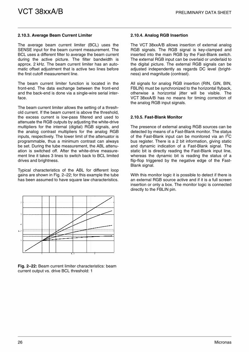
Typical characteristics of the ABL for different loopgains are shown in Fig. 2–22; for this example the tubehas been assumed to have square law characteristics.
Fig. 2–22: Beam current limiter characteristics: beam current output vs. drive BCL threshold: 1
2.10.4. Analog RGB Insertion
The VCT 38xxA/B allows insertion of external analogRGB signals. The RGB signal is key-clamped andinserted into the main RGB by the Fast-Blank switch.The external RGB input can be overlaid or underlaid tothe digital picture. The external RGB signals can beadjusted independently as regards DC level (bright-ness) and magnitude (contrast).
All signals for analog RGB insertion (RIN, GIN, BIN,FBLIN) must be synchronized to the horizontal flyback,otherwise a horizontal jitter will be visible. TheVCT 38xxA/B has no means for timing correction ofthe analog RGB input signals.
2.10.5. Fast-Blank Monitor
The presence of external analog RGB sources can bedetected by means of a Fast-Blank monitor. The statusof the Fast-Blank input can be monitored via an I2Cbus register. There is a 2 bit information, giving staticand dynamic indication of a Fast-Blank signal. Thestatic bit is directly reading the Fast-Blank input line,whereas the dynamic bit is reading the status of aflip-flop triggered by the negative edge of the Fast-Blank signal.
With this monitor logic it is possible to detect if there isan external RGB source active and if it is a full screeninsertion or only a box. The monitor logic is connecteddirectly to the FBLIN pin.

PRELIMINARY DATA SHEET VCT 38xxA/B
Micronas 27
Fig. 2–23: Video back-end
ext.
cont
rast
*w
hite
driv
e R
*be
am c
urre
nt li
m.
cuto
ff R
DACVideo
blank &
timing
ADCmeasurm.
U/I-DAC
clampkey
analogR in
Sense
analogR out
analogG out
analogB out
analogG in
analogB in
mea
sure
men
t b
uffe
r
digitalR in
H V
measurem.DAC
ext.
brig
htne
ss *
whi
te d
rive
R
digitalG in
digitalB in
DAC
DACVideo
DACVideo
U/I-DAC U/I-DAC
cuto
ff G
DACcu
toff
B
DAC
DAC DAC
InputI/O
ext.
brig
htne
ss *
whi
te d
rive
G
ext.
brig
htne
ss *
whi
te d
rive
B
DAC
whi
te d
rive
G
DAC
int.
brig
htne
ss *
whi
te d
rive
B
DAC
whi
te d
rive
Rin
t. br
ight
ness
*in
t. br
ight
ness
*
fast
ext.
cont
rast
*w
hite
driv
e G
*be
am c
urre
nt li
m.
ext.
cont
rast
*w
hite
driv
e B
*be
am c
urre
nt li
m.
analogSVM out
DACSVM
I0
digitalSVM in
serial interface
clamp clamp
blank in
blanking
blanking
blanking
ext. brightness
ext. contrast
int . brightness
white drive B
white drive G
white drive R

VCT 38xxA/B PRELIMINARY DATA SHEET
28 Micronas
2.11. Synchronization and Deflection
The synchronization and deflection processing is dis-tributed over front-end and back-end. The videoclamping, horizontal and vertical sync separation andall video related timing information are processed inthe front-end. Most of the processing that runs at thehorizontal frequency is programmed on the internalFast Processor (FP). Also the values for vertical andEast/West deflection are calculated by the FP soft-ware.
The generation of horizontal and vertical drive signalscan be synchronized to the video timing extracted inthe front-end or to a free running line counter in theback-end.
2.11.1. Deflection Processing
The deflection processing generates the signals for thehorizontal and vertical drive (see Fig. 2–24). This blockcontains two phase-locked loops:
– PLL2 generates the horizontal and vertical timing, e.g. blanking, clamping and composite sync. Phase and frequency are synchronized by the front sync signal.
– PLL3 adjusts the phase of the horizontal drive pulse and compensates for the delay of the horizontal out-put stage. Phase and frequency are synchronized by the oscillator signal of PLL2.
The horizontal drive circuitry uses a digital sine wavegenerator to produce the exact (subclock) timing forthe drive pulse HOUT. The generator runs at 1 MHz.Under control of the EHPLL bit and the internal voltagesupervision it is either synchronized by the deflectionPLL or it is free running. In the output stage the fre-quency is divided down to give drive-pulse period andwidth. The drive pulse width is programmable. Thehorizontal drive uses an open drain output transistor.
After power on or during reset the HOUT generation isswitched to a free running mode with a fix duty cycle of50%. For normal operation the EHPLL bit has to be setfirst. During the switch the actual period of HOUT canvary by up to 1 µs.
2.11.2. Angle and Bow Correction
The Angle and Bow correction is part of the horizontaldrive PLL. This feature allows a shift of the horizontaldrive pulse phase depending on the vertical positionon the screen. The phase correction has a linear(angle) and a quadratic term (bow).
2.11.3. Horizontal Phase Adjustment
This section describes a simple way to align PLLphases and the horizontal frame position.
1. With HDRV the duration of the horizontal drive pulse has to be adjusted
2. With POFS2 the delay between input video and dis-play timing (e.g. clamping pulse for analog RGB) has to be adjusted
3. With CSYDEL the delay between video and analog RGB (OSD) has to be adjusted.
4. With CSYDEL and HPOS the horizontal position of both, the digital and analog RGB signal (from SCART) relative to the clamping pulse has to be adjusted to the correct position, e.g. the pedestal of the generator signal.
5. With POFS3 the position of horizontal drive/flyback relative to RGB has to be adjusted
6. With NEWLIN the position of a scaled video picture can be adjusted (left, middle, center, etc; versions with panorama scaler only).
7. With HBST and HBSO, the start and stop values for the horizontal blanking have to be adjusted.
Note: The processing delay of the internal digital videopath differs depending on the comb filter option of theVCT 38xxA/B. The versions with comb filter have anadditional delay of 34 clock cycles.

PRELIMINARY DATA SHEET VCT 38xxA/B
Micronas 29
Fig. 2–24: Deflection processing block diagram
2.11.4. Vertical and East/West Deflection
The calculations of the vertical and East/West deflec-tion waveforms is done by the internal Fast Processor(FP). The algorithm uses a chain of accumulators togenerate the required polynomial waveforms. To pro-duce the deflection waveforms, the accumulators areinitialized at the beginning of each field. The initializa-tion values must be computed by the TV control pro-cessor and are written to the front-end once. Thewaveforms are described as polynomials in x, where xvaries from 0 to 1 for one field.
P: a + b(x-0.5) + c(x-0.5)2 + d(x-0.5)3 + e(x-0.5)4
The initialization values for the accumulators a0..a3 forvertical deflection and a0..a4 for East/West deflectionare 12-bit values.
Fig. 2–25 shows several vertical and East/West deflec-tion waveforms. The polynomial coefficients are alsostated.
In order to get a faster vertical retrace timing, the out-put impedance of the vertical D/A-converter can bereduced by 50% during the retrace.
2.11.5. EHT Compensation
The vertical waveform can be scaled according to theaverage beam current. This is used to compensate theeffects of electric high-tension changes due to beamcurrent variations. EHT compensation for East/Westdeflection is done with an offset corresponding to theaverage beam current.
PhaseComparator
&Low-pass
PLL2
E/Wcorrection
Sawtooth
PWM15-bit EW
VERT
VPROT
PWM15-bit
DCOFrontSync
InterfaceFSY
VDATA
MainSync
Generator
VerticalData
PhaseComparator
&Low-pass
PLL3
1:64&
OutputStage
HFLB
HOUTDCO
DisplayTiming
LineCounter
blanking, clamping, etc.
Clock & Control
SinewaveGenerator &
DAC
LPF
MSY
vertical reset
SkewMeasure-ment
Angle & Bow+
VERTQ
SyncGeneration
INTLC

VCT 38xxA/B PRELIMINARY DATA SHEET
30 Micronas
2.11.6. Protection Circuitry
Picture tube and drive stage protection is providedthrough the following measures:
– Vertical flyback protection input: This pin searches for a negative edge in every field, otherwise the RGB drive signals are blanked.
– Drive shutoff during flyback:This feature can be selected by software.
– Safety input pin:This input has two thresholds. Between zero and the lower threshold, normal functioning takes place. Between the lower and the higher threshold, the RGB signals are blanked. Above the higher thresh-old, the RGB signals are blanked and the horizontal drive is shut off. Both thresholds have a small hys-teresis.
–
2.12. Reset Function
Reset of all VDP functions is performed by the RESQpin. When this pin becomes active, all internal regis-ters and counters are lost. The TV controller can acti-vate the RESQ pin by software (see Section 5.7.2. onpage 95).
When the RESQ pin is released, the internal reset isstill active for 4 µs. After that time, the initialization ofall required registers is performed by the internal FastProcessor. This takes approximately 60 µs. During thisinitialization procedure it is not possible to access theVDP via the I2C interface.
The VDP voltage supervision activates an internalreset signal when the supply for the digital circuits(VSUPD) goes below ~2.5 V for more than 50 ns. Thisreset signal may be observed by the CPU (see Section5.7.3. on page 96).
Fig. 2–25: Vertical and East/West deflection waveforms
a,b,c,d,e0,0,1,0,00,0,0,0,10,0,1,1,1
East/West:a,b,c,d0,1,0,00,1,1,00,1,0,1
Vertical:

PRELIMINARY DATA SHEET VCT 38xxA/B
Micronas 31
2.14. I2C Bus Slave Interface
Communication between the video processing part ofthe VDP and the CPU is done via I2C bus. For detailedinformation on the I2C bus please refer to the Philipsmanual ‘I2C bus Specification’.
The VDP has two I2C bus slave interfaces (for compat-ibility with VPC/DDP applications) − one in thefront-end and one in the back-end. Both I2C bus inter-faces use I2C clock synchronization to slow down theinterface if required. Both I2C bus interfaces use onelevel of subaddress: the I2C bus chip address is usedto address the VDP and a subaddress selects one ofthe internal registers. The I2C bus chip addresses aregiven below:
The registers of the VDP have 8 or 16-bit data size;16-bit registers are accessed by reading/writing two8-bit data words.
Fig. 2–26 shows I2C bus protocols for read and writeoperations of the interface; the read operation requiresan extra start condition and repetition of the chipaddress with read command set.
2.14.1. Control and Status Registers
Table 2–3 gives definitions of the VDP control and sta-tus registers. The number of bits indicated for eachregister in the table is the number of bits implementedin hardware, i.e. a 9-bit register must always beaccessed using two data bytes but the 7 MSB will be‘don’t care’ on write operations and ‘0’ on read opera-tions. Write registers that can be read back are indi-cated in Table 2–3.
Functions implemented by software in the on-chip con-trol microprocessor (FP) are explained in Table 2–7.
A hardware reset initializes all control registers to 0.The automatic chip initialization loads a selected set ofregisters with the default values given in Table 2–3.
The register modes given in Table 2–3 are
– w: write only register
– w/r: write/read data register
– r: read data from VDP
– v: register is latched with vertical sync
– h: register is latched with horizontal
Fig. 2–26: I2C bus protocols
Table 2–2: I2C chip addresses
ChipAddress
A6 A5 A4 A3 A2 A1 A0 R/W
front-end 1 0 0 0 1 1 1 1/0
back-end 1 0 0 0 1 0 1 1/0
PS
10SDA
SCL
S
S
1000 111
1000 111
W Ack
AckW 0111 1100
0111 1100
Ack
Ack
S
1 or 2 byte Data
1000 111 R high byte Data
low byte Data
P
WRAckNakSP
======
0101StartStop
Ack
Nak P
I2C write accesssubaddress 7c
I2C read accesssubaddress 7c

VCT 38xxA/B PRELIMINARY DATA SHEET
32 Micronas
Table 2–3: I2C control and status registers of the video front-end
I2C Sub address
Number of bits
Mode Function Default Name
FP Interface
h’35 8 r FP statusbit [0] write requestbit [1] read requestbit [2] busy
FPSTA
h’36 16 w bit[8:0] 9-bit FP read addressbit[11:9] reserved, set to zero
FPRD
h’37 16 w bit[8:0] 9-bit FP write addressbit[11:9] reserved, set to zero
FPWR
h’38 16 w/r bit[11:0] FP data register, reading/writing to this register will autoincrement the FP read/write address. Only 16 bit of data aretransferred per I2C telegram.
FPDAT
Black Line Detector
h’12 16 r Available for versions with panorama scaler only!read only register, do not write to this register!after reading, LOWLIN and UPLIN are reset to 127 to start a new measurementbit[6:0] number of lower black linesbit[7] always 0bit[14:8] number of upper black linesbit[15] normal/black picture
BLKLIN
LOWLIN
UPLINBLKPIC
Miscellaneous
h’29 16 w/r Test pattern generator:bit[10:0] reserved (set to 0)bit[11] 0/1 disable/enable test pattern generatorbit[13:12] output mode:
00 Y/C = ramp (240 ... 17)01 Y/C = 1610 Y/C = 9011 Y/C = 240
bit[15:14] 0/1 reserved (set to 0)
000
0
TPG
TPGEN
TPGMODE
h’22 16 w/r NEWLINE: Available for versions with panorama scaler only!bit[10:0] NEWLINE register
This register defines the readout start ofthe next line in respect to the value of thesync counter.
bit [15:11] reserved (set to 0)
0NEWLIN
Table 2–4: I2C control and status registers of the video back-end. − default values are initialized at reset
I2C Sub address
Number of bits
Mode Function Default Name
Luminance Channel
h’61 9 w v bit [5:0] 0..63/32 main picture contrast 32 CTM

PRELIMINARY DATA SHEET VCT 38xxA/B
Micronas 33
h’65 9 w v bit [5:0] 0..63/32 side picture contrast 32 CTS
h’51 9 w v bit [8:0] −256..255 main picture brightness 0 BRM
h’55 9 w v bit [8:0] −256..255 side picture brightness 0 BRS
h’75 9 w v luma channel, priority mask registerbit [7:0] 0/1 select contrast, brightness, matrix
for main/side picture
0 PBCT 1)
h’71 9 w v luma channel, priority mask registerbit [7:0] 0/1 select main (video) / external (via CLUT)
RGB
0 PBERGB 1)
Black-Level Expander
h’59 9 w v black-level expanderbit [3:0] 0..15 tilt coefficientbit [8:4] 0...31 amount
812
BLE1BTLTBAM
h’5d 9 w v black-level expander, threshold:bit [8:0] 0..511 disable expansion, threshold value 200
BLE2BTHR
h’73 9 w v black-level expander, measurementbit [7:0] 0..255 vstart/2
start line = vstartstop line = 336/283 − vstart
or vertical blankingbit[8] 0/1 50/60 Hz measurement windowlength
15
0
BLE3BVST
BWL
h’7d 9 w v black-level expander, priority mask registerbit [7:0] 0/1 enable/disable black-level expander
0 PBBLE 1)
Dynamic Peaking
h’69 9 w v luma peaking filter, the gain at high frequencies and small signal amplitudes is: 1 + (k1+k2)/8bit [3:0] 0..15 k1: peaking level undershootbit [7:4] 0..15 k2: peaking level overshootbit [8] 0/1 peaking value normal/inverted
(peaking/softening)
440
PK1
PKUNPKOVPKINV
h’6d 9 w v luma peaking filter, coringbit [4:0] 0..31 coring levelbit [7:5] reservedbit [8] 0/1 peaking filter center frequency high/low
3
0
PK2COR
PFS
h’79 9 w v luma peaking filter, priority mask registerbit [7:0] 0/1 disable/enable peaking transient
suppression when signal is switched
0 PBPK 1)
1) priority mask registerIf bit[x] is set to 1 then the function is active for the respective signal priority
Table 2–4: I2C control and status registers of the video back-end. − default values are initialized at reset
I2C Sub address
Number of bits
Mode Function Default Name

VCT 38xxA/B PRELIMINARY DATA SHEET
34 Micronas
Soft Limiter
h’41 9 w v luma soft limiter, slope A and Bbit [3:0] slope segment Abit [7:4] slope segment B
00
LSL1LSLSALSLSB
h’45 9 w v luma soft limiter, absolute limitbit [7:0] luma soft limiter absolute limit
(unsigned)bit [8] 0/1 modulation off/on
255
1
LSL2LSLAL
LSLM
h’49 9 w v bit [8:0] luma soft limiter segment B tilt point (unsigned) 300 LSLTB
h’4d 9 w v bit [8:0] luma soft limiter segment A tilt point (unsigned) 250 LSLTA
Chrominance Channel
h’14 8 w/r luma/chroma matchingbit [2:0] −3...3 variable chroma delaybit [7:3] reserved, set to 0
0LCMCDEL
h’5e 9 w v digital transient improvementbit [3:0] 0..15 coring valuebit [7:4] 0..15 DTI gainbit [8] 0/1 narrow/wide bandwidth mode
151
DTIDTICODTIGADTIMO
Inverse Matrix
h’7ch’74
99
w vw v
main picture matrix coefficient R−Y = MR1M*CB + MR2M*CRbit [8:0] −256/128 ... 255/128bit [8:0] −256/128 ... 255/128
086
MR1M,MR2M
h’6ch’64
99
w vw v
main picture matrix coefficient G−Y = MG1M*CB + MG2M*CRbit [8:0] −256/128 ... 255/128bit [8:0] −256/128 ... 255/128
−22−44
MG1M,MG2M
h’5ch’54
99
w vw v
main picture matrix coefficient B−Y = MB1M*CB + MB2M*CRbit [8:0] −256/128 ... 255/128bit [8:0] −256/128 ... 255/128
1130
MB1M,MB2M
h’78h’70
99
w vw v
side picture matrix coefficient R−Y = MR1S*CB + MR2S*CRbit [8:0] −256/128 ... 255/128bit [8:0] −256/128 ... 255/128
073
MR1S,MR2S
h’68h’60
99
w vw v
side picture matrix coefficient G−Y = MG1S*CB + MG2S*CRbit [8:0] −256/128 ... 255/128bit [8:0] −256/128 ... 255/128
−19−37
MG1S,MG2S
h’58h’50
99
w vw v
side picture matrix coefficient B−Y = MB1S*CB + MB2S*CRbit [8:0] −256/128 ... 255/128bit [8:0] −256/128 ... 255/128
970
MB1S,MB2S
Table 2–4: I2C control and status registers of the video back-end. − default values are initialized at reset
I2C Sub address
Number of bits
Mode Function Default Name

PRELIMINARY DATA SHEET VCT 38xxA/B
Micronas 35
Color Lookup Table
h’00−h’0f
16 w h color look-up table: 16 entries, 12 bit wide,The CLUT registers are initialized at power-up bit [3:0] 0..15 blue amplitudebit [7:4] 0..15 green amplitudebit [11:8] 0..15 red amplitude
000hf00h0f0hff0h00fhf0fh0ffhfffh7ffh700h070h770h007h707h077h777h
CLUT0
CLUT15
h’4c 9 w v digital OSD insertion contrast for R (amplitude range: 0 to 255)bit [3:0] 0..13 R amplitude = CLUTn ⋅ (DRCT + 4)
14,15 invalid picture frame insertion contrast for R (ampl. range: 0 to 255)bit [7:4] 0..13 R amplitude = PFCR ⋅ (PFRCT + 4)
14,15 invalid
8
8
RCTDRCT
PFRCT
h’48 9 w v digital OSD insertion contrast for G (amplitude range: 0 to 255)bit [3:0] 0..13 G amplitude = CLUTn ⋅ (DGCT + 4)
14,15 invalid picture frame insertion contrast for G (ampl. range: 0 to 255)bit [7:4] 0..13 G amplitude = PFCG ⋅ (PFGCT + 4)
14,15 invalid
8
8
GCTDGCT
PFGCT
h’44 9 w v digital OSD insertion contrast for B (amplitude range: 0 to 255)bit [3:0] 0..13 B amplitude = CLUTn ⋅ (DBCT + 4)
14,15 invalid picture frame insertion contrast for B (ampl. range: 0 to 255)bit [7:4] 0..13 B amplitude = PFCB ⋅ (PFBCT + 4)
14,15 invalid
8
8
BCTDBCT
PFBCT
Picture Frame Generator
h’11 16 w/r picture frame colorbit [3:0] 0..15 blue amplitudebit [7:4] 0..15 green amplitudebit [11:8] 0..15 red amplitude
000
PFCPFCBPFCGPFCR
h’47 9 w v bit [2:0] picture frame generator priority idbit [8] enable prio id for picture frame generator
0 PFGIDPFGEN
h’4F 9 w v bit [8:0] horizontal picture frame begincode 0 = picture frame generator horizontally disabledcode 1FF = full frame
0 PFGHB
h’53 9 w v bit [8:0] horizontal picture frame end 0 PFGHE
h’63 9 w v bit [8:0] vertical picture frame begincode 0 = picture frame generator vertically disabled
270 PFGVB
Table 2–4: I2C control and status registers of the video back-end. − default values are initialized at reset
I2C Sub address
Number of bits
Mode Function Default Name

VCT 38xxA/B PRELIMINARY DATA SHEET
36 Micronas
h’6f 9 w v bit [8:0] vertical picture frame end 56 PFGVE
Scan Velocity Modulation
h’5a 9 w v video mode coefficientsbit [5:0] gain1bit [8:6] differentiator delay 1 (0= filter off, 1...6= delay)
604
SVM1SVG1SVD1
h’56 9 w v text mode coefficientsbit [5:0] gain 2bit [8:6] differentiator delay 2 (0= filter off, 1...6= delay)
604
SVM2SVG2SVD2
h’52 9 w v limiterbit [6:0] limit valuebit [8:5] not used, set to “0”
1000
SVM3SVLIM
h’4e 9 w v delay and coringbit [3:0] adjustable delay, in 1/2 display clock steps,
(value 5 : delay of SVMOUT is the same as forRGBOUT
bit [7:4] coring valuebit [8] not used, set to “0”
7
0
SVM4SVDEL
SVCOR
Display Controls
h’4ah’46h’42
999
w vw vw v
cutoff Redcutoff Greencutoff Blue
000
CRCGCB
Tube- and Picture-Measurements
h’7b 9 w v picture measurement start linebit [8:0] (TML+9)..511 first line of picture measurement 23
PMST
h’6b 9 w v picture measurement stop linebit [8:0] (PMST+1)..511 last line of picture measurement 308
PMSO
h’7f 9 w v tube measurement linebit [8:0] 0..511 start line for tube measurement 15
TML
h’25 8 w/r tube and picture measurement controlbit [0] 0/1 disable/enable tube measurementbit [1] 0/1 80/40 kHz bandwidth for
picture measurementbit [2] 0/1 disable/enable picture measurement
(writing a ’1’ starts one measurement cycle)
bit [3] 0/1 large/small picture measurement window,will be disabled from bit[3] in address h’32
bit [4] 0/1 measure / offset check for adcbit [7:5] reserved
0 TPMTMENPMBW
PMEN
PMWIN
OFSEN
h’13 16 w/r white drive measurement controlbit [9:0] 0..1023 RGB values for white drive beam current
measurementbit [10] reservedbit [11] 0/1 RGB values for white drive beam current
measurement disabled/enabled
512
0
WDMWDRV
EWDM
Table 2–4: I2C control and status registers of the video back-end. − default values are initialized at reset
I2C Sub address
Number of bits
Mode Function Default Name

PRELIMINARY DATA SHEET VCT 38xxA/B
Micronas 37
h’18h’19h’1ah’1dh’1ch’1b
8 r measurement result registersminimum in active picturemaximum in active picturewhite drive cutoff/leakage redcutoff/leakage greencutoff/leakage blue,read pulse starts tube measurement
−MRMINMRMAXMRWDRMRCRMRCGMRCB
h’1e 8 r measurement adc status and Fast-Blank input status
measurement status registerbit [0] 0/1 tube measurement active / completebit [2:1] white drive measurement cycle
00 red01 green10 blue11 reserved
bit [3] 0/1 picture measurement active / completebit [4] 0/1 Fast-Blank input Low / High (static)bit [5] 1 Fast-Blank input negative transition since
last read (bit reset at read)bit [7:6] reserved
− PMS
TUMSWDRMC
PIMSFBLEVFBSLO
Vertical Timing
h’67 9 w v vertical blanking startbit [8:0] 0..511 first line of vertical blanking 305
VBST
h’77 9 w v vertical blanking stopbit [8:0] 0..511 last line of vertical blanking 25
VBSO
h’5f 9 w v vertical free run periodbit [8:0] free running field period = (value+4) lines 309
VPER
Horizontal Deflection and Timing
h’7a 9 w v quadratic term of angle & bow correctionbit [8:0] −256..+255 (± 500 ns)
0 BOW
h’76 9 w v linear term of angle & bow correctionbit [8:0] −256..+255 (± 500 ns)
0 ANGLE
h’6e 9 w v adjustable delay of PLL2, clamping, and blanking (relative to front sync)adjust clamping pulse for analog RGB inputbit [8:0] −256..+255 (± 8 µs)
−141 POFS2
h’72 9 w v adjustable delay of flyback, main sync, csync and analog RGB (relative to PLL2)adjust horizontal drive or csyncbit [8:0] −256..+255 (± 8 µs)
0 POFS3
h’7e 9 w v adjustable delay of main sync (relative to flyback)adjust horizontal position for digital picturebit [8:0] 20 steps=1 µs
120 HPOS
Table 2–4: I2C control and status registers of the video back-end. − default values are initialized at reset
I2C Sub address
Number of bits
Mode Function Default Name

VCT 38xxA/B PRELIMINARY DATA SHEET
38 Micronas
t
h’5b 9 w v start of horizontal blankingbit [8:0] 0..511
1 HBST
h’57 9 w v end of horizontal blankingbit [8:0] 0..511
48 HBSO
h’62h’66h’6a
999
w vw vw v
PLL2/3 filter coefficients, 1of5 bit code (n+ set bit number)bit [5:0] proportional coefficient PLL3, 2−n−1
bit [5:0] proportional coefficient PLL2, 2−n−1
bit [5:0] integral coefficient PLL2, 2−n−5
212
PKP3PKP2PKI2
h’15 16 w/r horizontal drive and vertical signal control registerbit [5:0] 0..63 horizontal drive pulse duration in µs
(internally limited to 4..61)bit [6] 0/1 disable/enable horizontal PLL2 and PLL3bit [7] 0/1 1: disable horizontal drive pulse during
flybackbit [8] reserved, set to ’0’bit [9] 0/1 enable/disable ultra black blankingbit [10] 0/1 0: all outputs blanked
1: normal modebit [11] 0/1 enable/disable clamping for analog RGB
inputbit [12] 0/1 disable/enable vertical free running mode
(FIELD is set to field2, no interlace)bit [13] 0/1 enable/disable vertical protectionbit [14] reserved, set to ’0’bit [15] 0/1 disable/enable phase shift of display clock
32
00
001
0
0
001
HVCHDRV
EHPLLEFLB
DUBLEBL
DCRGB
SELFT
DVPR
DISKA
h’9d 8 w/r sync output controlbit [0] invert INTLCbit [4:1] reserved, set to ’0’bit [5] force INTLC to polarity defined in ‘INTLCINV’
0 SYCTRLINTLCINV
INTL-CFRC
Miscellaneous
h’32 8 w/r Fast-Blank interface modebit [0] 0 internal Fast-Blank from FBLIN pin
1 force internal Fast-Blank signal to Highbit [1] 0/1 internal Fast-Blank active High/Lowbit [2] 0/1 disable/enable clamping reference for
RGB outputsbit [3] 1 full line MADC measurement window,
disables bit [3] in address h’25bit [4] 0/1 horizontal flyback input active High/Lowbit [6:5] reserved (set to 0)bit [7] vertical output select
0 VERTQ output1 INTLC output
0 FBMODFBFOH
FBPOLCLMPR
FLMW
FLPOL
VOS
h’4b 9 w v Fast-Blank input, priority mask registerbit [7:0] 0/1 disable/enable analog Fast-Blank input
0 PBFB 1)
Table 2–4: I2C control and status registers of the video back-end. − default values are initialized at reset
I2C Sub address
Number of bits
Mode Function Default Name

PRELIMINARY DATA SHEET VCT 38xxA/B
Micronas 39
Table 2–5: Control registers of the Fast Processor for control of the video front-end functions
FP Sub-address
Function Default Name
Standard Selection
h’20 Standard select:bit[2:0] standard
0 PAL B,G,H,I (50 Hz) 4.4336181 NTSC M (60 Hz) 3.5795452 SECAM (50 Hz) 4.2863 NTSC44 (60 Hz) 4.4336184 PAL M (60 Hz) 3.5756115 PAL N (50 Hz) 3.5820566 PAL 60 (60 Hz) 4.4336187 NTSC COMB (60 Hz) 3.579545
bit[3] 0/1 standard modifierPAL modified to simple PALNTSC modified to compensated NTSCSECAM modified to monochrome 625NTSCC modified to monochrome 525
bit[4] reserved (set to 0)bit[5] 0/1 2-H comb filter off/onbit[6] 0/1 S-VHS mode off/on (2-H comb is switched off)
Option bits allow to suppress parts of the initialization, this can be used for color standard search:
bit[7] no hpll setupbit[8] no vertical setupbit[9] no acc setupbit[10] 2-H comb filter set-up only
bit[11] status bit, normally write 0. After the FP has switched to a new standard, this bit is set to 1 to indicate operation complete. Standard is automatically initialized when the insel register is written.
0 SDT
PALNTSCSECAMNTSC44PALMPALNPAL60NTSCCSDTMOD
COMBSVHS
SDTOPT
h’148 Enable automatic standard recognition (ASR)bit[0] 0/1 PAL B,G,H,I (50 Hz) 4.433618bit[1] 0/1 NTSC M (60 Hz) 3.579545bit[2] 0/1 SECAM (50 Hz) 4.286bit[3] 0/1 NTSC44 (60 Hz) 4.433618bit[4] 0/1 PAL M (60 Hz) 3.575611bit[5] 0/1 PAL N (50 Hz) 3.582056bit[6] 0/1 PAL 60 (60 Hz) 4.433618bit[10:7] reserved set to 0bit[11] 1 reset status information ‘switch’ in asr_status
(cleared automatically)
0: disable recognition; 1: enable recognitionNote: For correct operation don’t change FP reg. 20h and 21h, while ASR is enabled!
0 ASR_ENA

VCT 38xxA/B PRELIMINARY DATA SHEET
40 Micronas
h’14e Status of automatic standard recognitionbit[0] 1 error of the vertical standard (neither 50 nor 60 Hz)bit[1] 1 detected standard is disabledbit[2] 1 search activebit[3] 1 search terminated, but failedbit[4] 1 no color foundbit[5] 1 standard has been switched (since last reset of this
flag with bit[11] of asr_enable)
bit[4:0] 00000 all ok00001 search not started, because vwin error detected
(no input or SECAM L)00010 search not started, because detected vert. standard
not enabled0x1x0 search started and still active01x00 search failed (found standard not correct)01x10 search failed, (detected color standard not enabled)10000 no color found (monochrome input or switch betw.
CVBS/SVHS necessary)
0 ASR_STATUSVWINERRDISABLEDBUSYFAILEDNOCOLORSWITCH
h’21 Input select: writing to this register will also initialize the stan-dardbit[1:0] luma selector
00 VIN101 VIN210 VIN311 VIN4
bit[2] chroma selector0 CIN11 CIN2
bit[4:3] IF compensation00 off01 6 dB/Oct10 12 dB/Oct11 10 dB/MHz only for SECAM
bit[6:5] chroma bandwidth selector00 narrow01 normal10 broad11 wide
bit[7] 0/1 adaptive/fixed SECAM notch filterbit[8] Available for versions with panorama scaler only!
0 disable luma lowpass filter1 enable luma lowpass filter
bit[10:9] hpll speed00 no change01 terrestrial10 vcr11 mixed
bit[11] status bit, write 0, this bit is set to 1 to indicate operation complete.
00
0
00
01
INSEL
VIS
CIS
IFC
CBW
FNTCHLOWP
HPLLMD
h’22 Available for versions with panorama scaler only!
picture start position, this register sets the start point of active video, this can be used e.g. for panning. The setting is updated when ’sdt’ register is updated.
0 SFIF
Table 2–5: Control registers of the Fast Processor for control of the video front-end functions
FP Sub-address
Function Default Name

PRELIMINARY DATA SHEET VCT 38xxA/B
Micronas 41
h’23 luma/chroma delay adjust. The setting is updated when ’sdt’ register is updated.bit[5:0] reserved, set to zerobit[11:6] luma delay in clocks, allowed range is +1 ... −7
0 LDLY
h’2f YCrCb mode control registerbit[3:0] reserved (set to 0)bit[4] Available on VCT 38xxB only!
0 disable YC adder1 enable YC adder
bit[5] Available on VCT 38xxB only!0 video input 5 disable (pin P10 = P10)1 video input 5 enable (pin P10 = VIN5)
bit[6] Available on VCT 38xxB only!0 video input = VIN1-4 (depending on VIS setting)1 video input = VIN5
bit[7] clipping due to ADC over-/underflow(has to be reset after read if used)
bit[8] 0 disable YCrCb1 enable YCrCb
bit[9] ADC range0 nominal input amplitude (±350 mV)1 extended input amplitude (±500 mV)
bit[11:10] reserved (set to 0)
Note: Activate the YCrCb mode by− enabling YCrCb− selecting simple PAL or NTSC M, svhs=1, comb=0 in the std register− setting cbw=2 in the insel register
0 YCrCb
YCADD
VIN5EN
VIN5SEL
ADCCLIP
YCrCb_EN
ADCR
Comb Filter
h’27 comb filter control register bit[0] 0 comb coefficients are calculated for luma/chroma
1 comb coefficients for luma are used for luma and chroma
bit[1] 0 luma comb strength depends on signal amplitude1 luma comb strength is independent of amplitude
bit[2] 0 reduced comb booster1 max comb booster
bit[4:3] 0..3 comb strength for chroma signalbit[6:5] 0..3 comb strength for luma signalbit[11:7] 0..31 overall limitation of the calculated comb coefficients
0 no limitation31 max limitation (1/2)
0
0
1
320
CMB_UCCC
DAA
KB
KCKYCLIM
Color Processing
h’30 Saturation controlbit[11:0] 0...4094 (2070 corresponds to 100% saturation)
4095 disabled (test mode only)
2070 ACC_SAT
h’17a bit[10:0] 0...2047 CR-attenuation
bit[11] 0/1 disable/enable CR-attenuation
1591
o
CR_ATT
CR_ATT_ENA
h’39 bit[10:0] 0...2047 amplitude killer level (0: killer disabled)bit[11] 0/1 disable/enable chroma ADC
250
KILVLECADC
h’3a amplitude killer hysteresis 5 KILHY
Table 2–5: Control registers of the Fast Processor for control of the video front-end functions
FP Sub-address
Function Default Name

VCT 38xxA/B PRELIMINARY DATA SHEET
42 Micronas
h’dc NTSC tint angle, ±512 = ±π/4 0 TINT
DVCO
h’f8 crystal oscillator center frequency adjust, −2048 ... 2047 −720 DVCO
h’f9 crystal oscillator center frequency adjustment value for line-lock modeTrue adjust value is DVCO − ADJUST. For factory crystal alignment, using standard video signal: set DVCO = 0, set lock mode, read crystal offset from ADJUST register and use negative value for initial center frequency adjustment via DVCO.
read only ADJUST
h’f7 crystal oscillator line-locked mode, lock command/statuswrite: 100 enable lock
0 disable lockread: 0 unlocked
>2047 locked
0 XLCK
h’b5 crystal oscillator line-locked mode, autolock feature. If autolock is enabled, crystal oscillator locking is started automatically.bit[11:0] threshold; 0: autolock off
400 AUTOLOCK
FP Status
h’12 general purpose control bitsbit[2:0] reserved, do not changebit[3] vertical standard forcebit[8:4] reserved, do not changebit[9] disable flywheel interlacebit[11:10] reserved, do not changeto enable vertical free run mode set vfrc to 1 and dflw to 0
0
1
GPC
VFRC
DFLW
h’13 standard recognition statusbit[0] 1 vertical lockbit[1] 1 horizontally lockedbit[2] 1 no signal detectedbit[3] 1 color amplitude killer activebit[4] 1 disable amplitude killerbit[5] 1 color ident killer activebit[6] 1 disable ident killerbit[7] 1 interlace detectedbit[8] 1 no vertical sync detectionbit[9] 1 spurious vertical sync detectionbit[11:10] reserved
− ASR
h’14 input noise level read only NOISE
h’cb number of lines per field, P/S: 312, N: 262 read only NLPF
h’15 vertical field counter, incremented per field read only VCNT
h’74 measured sync amplitude value, nominal: 768 (PAL), 732 (NTSC) read only SAMPL
h’36 measured burst amplitude read only BAMPL
h’f0 firmware version numberbit[7:0] internal revision numberbit[11:8] firmware release
read only SW_VERSION
Table 2–5: Control registers of the Fast Processor for control of the video front-end functions
FP Sub-address
Function Default Name

PRELIMINARY DATA SHEET VCT 38xxA/B
Micronas 43
h’f1 hardware version numberbit[6:0] reservedbit[11:7] bond option
bit[7] 0/1 16k text memory on/offbit[8] 0/1 VDP platform full/litebit[9] 0/1 picture improvements on/offbit[10] 0/1 panorama scaler on/offbit[11] 0/1 comb filter on/off
read only HW_VERSION
h’170 status of MCV detectionbit[0] AGC pulse detectedbit[1] pseudo sync detected
read only MCV_STATUS
h’171 bit[11:0] first line of MCV detection window 6 MCV_START
h’172 bit[11:0] last line of MCV detection window 15 MCV_STOP
Horizontal Scaler
1) these registers are updated when the scaler mode register is written
h’40 scaler mode registerbit[1:0] scaler mode
0 linear scaling mode1 nonlinear scaling mode, ’panorama’2 nonlinear scaling mode, ’waterglass’3 reserved
bit[10:2] reserved, set to 0bit[11] scaler update
0 start scaler update command,when the registers are updated the bit is set to 1
0 SCMODEMODE
SCUP
h’41 luma offset register 1)
bit[6:0] luma offset 0..127ITU-R output format: 57CVBS output format: 4
57 YOFFS
h’42 active video length for 1-h FIFO 1)
bit[11:0] length in pixels1080 FFLIM
h’43 scaler1 compression coefficient 1)
For compression by a factor c the value c*1024 is required.bit[11:0] allowed values from 1024..4095
1024 SCINC1
h’44 scaler2 expansion coefficient 1)
For expansion by a factor c the value 1/c*1024 is required.bit[11:0] allowed values from 256..1024
1024 SCINC2
h’45 scaler1/2 nonlinear scaling coefficient 1) 0 SCINC
h’47 −h’4b
scaler1 window controls 1)
5 12-bit registers for control of the nonlinear scaling0 SCW1_0 − 4
h’4c −h’50
scaler2 window controls 1)
5 12-bit registers for control of the nonlinear scaling0 SCW2_0 − 4
Table 2–5: Control registers of the Fast Processor for control of the video front-end functions
FP Sub-address
Function Default Name

VCT 38xxA/B PRELIMINARY DATA SHEET
44 Micronas
2.14.1.1. Scaler Adjustment
In case of linear scaling, most of the scaler registersneed not be set. Only the scaler mode, active videolength, and the fixed scaler increments (scinc1/scinc2)must be written.
The adjustment of the scaler for nonlinear scalingmodes should use the parameters given in Table 2–6.
Table 2–6: Set-up values for nonlinear scaler modes
Register Scaler Modes
‘waterglass’border 35%
‘panorama’border 30%
center compression
3/4 5/6 4/3 6/5
scinc1 1643 1427 1024 1024
scinc2 1024 1024 376 611
scinc 90 56 85 56
fflim 945 985 921 983
scw1 − 0 110 115 83 94
scw1 − 1 156 166 147 153
scw1 − 2 317 327 314 339
scw1 − 3 363 378 378 398
scw1 − 4 473 493 461 492
scw2 − 0 110 115 122 118
scw2 − 1 156 166 186 177
scw2 − 2 384 374 354 363
scw2 − 3 430 425 418 422
scw2 − 4 540 540 540 540

PRELIMINARY DATA SHEET VCT 38xxA/B
Micronas 45
Table 2–7: Control Registers of the Fast Processor for controlling the video back-end functions − default values are initialized at reset
FP Sub-address
Function Default Name
FP Display Control Register
h’130 White Drive Red (0...1023) 700 WDR 1)
h’131 White Drive Green (0...1023) 700 WDG 1)
h’132 White Drive Blue (0...1023) 700 WDB 1)
h’139 Internal Brightness, Picture (0...511), the center value is 256, the range allows for both increase and reduction of brightness.
256 IBR
h’13c Internal Brightness, Measurement (0...511), the center value is 256, the brightness for measurement can be set to measure at higher cutoff cur-rent. The measurement brightness is independent of the drive values.
256 IBRM
h’13a Analog Brightness for external RGB (0...511), the center value is 256, the range allows for both increase and reduction of brightness.
256 ABR
h’13b Analog Contrast for external RGB (0...511) 350 ACT
1) The white drive values will become active only after writing the blue value WDB, latching of new values is indi-cated by setting the MSB of WDB.
FP Display Control Register, BCL
h’144 BCL threshold current, 0...2047 (max ADC output ~1152) 1000 BCLTHR
h’142 BCL time constant 0...15 13...1700 msec 15 BCLTM
h’143 BCL loop gain. 0..15 0 BCLG
h’145 BCL minimum contrast 0...1023 307 BCLMIN
h’105 Test register for BCL/EHT comp. function, register value:0 normal operation1 stop ADC offset compensationx>1 use x in place of input from Measurement ADC
0 BCLTST
h’60 Current BCL reduction (0...1023) read only BCLREDUC
FP Display Control Register, Deflection
h’103 interlace offset, −2048..2047This value is added to the SAWTOOTH output during one field.
0 INTLC
h’102 discharge sample count for deflection retrace,SAWTOOTH DAC output impedance is reduced for DSCC lines after ver-tical retrace.
7 DSCC
h’11f vertical discharge value,SAWTOOTH output value during discharge operation, typically same as A0 init value for sawtooth.
−1365 DSCV
h’10b EHT compensation vertical gain coefficient, 0...511 0 EHTV
h’10a EHT compensation time constant, 0...15 --> 3.2.410 misc. 15 EHTTM
h’10f EHT compensation east/west gain coefficient, −1024...1023 15 EHTEW

VCT 38xxA/B PRELIMINARY DATA SHEET
46 Micronas
2.14.1.2. Calculation of Vertical and East-West Deflection Coefficients
In Table 2–8 the formula for the calculation of thedeflection initialization parameters from the polynomi-nal coefficients a, b, c, d, e is given for the vertical andEast-West deflection. Let the polynomial be:
The initialization values for the accumulators a0..a3 forvertical deflection and a0..a4 for East-West deflectionare 12-bit values. The coefficients that should be usedto calculate the initialization values for different fieldfrequencies are given below, the values must bescaled by 128, i.e. the value for a0 of the 50 Hz verticaldeflection is
FP Display Control Register, Vertical Sawtooth
h’110 DC offset of SAWTOOTH outputThis offset is independent of EHT compensation.
0 OFS
h’11b accu0 init value −1365 A0
h’11c accu1 init value 900 A1
h’11d accu2 init value 0 A2
h’11e accu3 init value 0 A3
FP Display Control Register, East-West Parabola
h’12b accu0 init value −1121 A0
h’12c accu1 init value 219 A1
h’12d accu2 init value 479 A2
h’12e accu3 init value −1416 A3
h’12f accu4 init value 1052 A4
Table 2–7: Control Registers of the Fast Processor for controlling the video back-end functions − default values are initialized at reset
FP Sub-address
Function Default Name
P = a + b(x – 0.5) + c(x – 0.5)2 + d(x – 0.5)3 + e(x – 0.5)4
a0 = (a · 128 – b · 1365.3 + c · 682.7 – d · 682.7) / 128

PRELIMINARY DATA SHEET VCT 38xxA/B
Micronas 47
Table 2–8: Calculation of Initialization values for Vertical Sawtooth and East-West Parabola
Vertical Deflection 50 Hz
a b c d
a0 128 –1365.3 +682.7 –682.7
a1 899.6 –904.3 +1363.4
a2 296.4 –898.4
a3 585.9
Vertical Deflection 60 Hz
a b c d
a0 128 –1365.3 +682.7 –682.7
a1 1083.5 –1090.2 +1645.5
a2 429.9 –1305.8
a3 1023.5
East-West Deflection 50 Hz
a b c d e
a0 128 –341.3 1365.3 –85.3 341.3
a1 111.9 –899.6 84.8 –454.5
a2 586.8 –111.1 898.3
a3 72.1 –1171.7
a4 756.5
East-West Deflection 60 Hz
a b c d e
a0 128 –341.3 1365.3 –85.3 341.3
a1 134.6 –1083.5 102.2 –548.4
a2 849.3 –161.2 1305.5
a3 125.6 –2046.6
a4 1584.8

VCT 38xxA/B PRELIMINARY DATA SHEET
48 Micronas
3. Text and OSD Processing
3.1. Introduction
The VCT 38xxA/B includes a World System Teletext(WST) decoder, whose display capabilities are alsoused for OSD generation. In the following sections thetext and OSD processing part of the VCT 38xxA/B willbe named TPU for short.
With integrated CPU, RAM and ROM, an adaptivedata slicer, a display controller, and a number of inter-faces, the TPU offers acquisition and display of variousteletext and data services such as WST, PDC, VPS,and WSS. Fig. 3–1 shows the functional block diagramof the TPU.
The TPU operates independently from the TV control-ler and can be controlled by software via I2C bus inter-face (see Section 3.14. on page 85). The TV control-ler is not burdened with the task of teletext decodingand communicates with the TPU via a high-level com-mand language.
The TPU performs the following tasks:
– teletext data acquisition (hardware)
– teletext data decoding (software)
– page generation (software)
– page memory management (software)
– page display (hardware)
– user interface (software)
3.2. SRAM Interface
The SRAM interface connects a standard SRAM to theinternal bus structure. The address bus is 19 bit wide,addressing SRAMs up to 4 Mbit. Smaller SRAMs canalso be connected.
The SRAM interface has to handle 3 asynchronousdata streams. The CPU needs access to every mem-ory location of the SRAM. During VBI the slicer writesup to 22 teletext lines of 43 Bytes into the acquisitionscratch memory. During text display the display con-troller copies teletext rows from display memory into itsinternal row buffer.
On VCT 38xxA/B the SRAM interface of the TPU isconnected to the memory bus of the TV controller. Thisis done to save pins and to give the TV controller fasteraccess to the display memory. Refer to DMA Interface(chapter 5.9. on page 101) for more details.
After reset the TPU will not use the SRAM interfaceuntil receiving the I2C command “DRAM_MODE” (seeSection 3.12. on page 70).
3.3. Text Controller
The TPU operates with its own 65C02 core running at10.125 MHz. The core can address up to 64 kBytes ofmemory.
The CPU memory contains 640 Bytes RAM, 12 kBytesprogram ROM and 12 kBytes character ROM. TheVCT 38xxB contains additional 12kBytes characterROM. The character ROM holds the font data and isseparated from the program ROM to save CPU time.The CPU can still access the character ROM via aDMA interface including wait cycles. The display con-troller can also access the CPU memory via the sameDMA interface. By this means it is possible to locatepart of the character font in program ROM or part ofthe program code in character ROM.
After Reset the CPU switches to external font memoryif the Font ID vector exists in the external font memory.After Reset the CPU switches to external programmemory if the Prog ID vector exists in the external pro-gram memory.
Table 3–1: Memory map of text controller
Memory Vector Absolute Address(High Byte, Low Byte)
IRQ FFFF, FFFE
Reset FFFD, FFFC
NMI FFFB, FFFA
Control Word FFF9
Prog ID (=A55A) FFF7, FFF6
Font ID (=A55A) 1001, 1000
Memory Segment Absolute Address
Zero Page 0000 − 00FF
Stack Page 0100 − 01FF
OSD Buffer 0100 − 019F
I/O Page 0200 − 02FF
Extra Page 0300 − 037F
Character ROM 5000 − 7FFF (VCT38xxA)2000 − 7FFF (VCT38xxB)
Program ROM D000 − FFFF

PRELIMINARY DATA SHEET VCT 38xxA/B
Micronas 49
Fig. 3–1: Block diagram of the TPU
TPU
WSTLayer
65C02
DMAInterface
CharacterROM
ProgramROM
ProgramRAM
ADCClampingAGC
I2C BusInterface
TimerInterruptWatchdog
Slicer
OSDLayer
SyncInterface
Color &PrioInterface
SRAMInterface

VCT 38xxA/B PRELIMINARY DATA SHEET
50 Micronas
Fig. 3–2: Memory environment of text controller
3.4. Teletext Acquisition
The only task of the slicer circuit is to extract teletextlines from the incoming composite video signal and tostore them into the acquisition scratch buffer of theinternal/external SRAM. No page selection is done atthis hardware level.
Four analog sources can be connected, thus it is pos-sible to receive text from one channel while watchinganother on the screen. After clamping and AGC ampli-fier the analog video signal is converted into binarydata. Sync separation is done by a sync slicer and ahorizontal PLL, which generate the horizontal and ver-tical timing. By these means, no external sync signalsare needed and any available signal source can beused for teletext reception.
The teletext information itself is acquired using adap-tive slicers on bit and byte level with soft error detec-tion to decrease the bit error rate under bad receptionconditions. The slicer can be programmed to differentbit rates for reception of PAL, NTSC or MAC worldsystem teletext as well as VPS, WSS, or CAPTIONsignals.
3.5. Teletext Page Management
As a state-of-the-art teletext decoder, the TPU is ableto store and manage a sufficient number of teletextpages to absorb the annoying transmission cycletimes. The number of available pages is only limited bythe memory size. With an intelligent software and a4-Mbit SRAM it is possible to store and to control morethan 500 teletext pages.
The management of such a data base is a typical soft-ware task and is therefore performed by the 65C02.Using a fixed length page table with one entry forevery possible page, the software distributes the con-tent of the acquisition scratch buffer among the pagememory. The page size is fixed to 1 kByte, only ghostrows are chained in 128-Byte segments to avoidunused memory space.
A stored teletext page cannot be displayed directly,because of the row-adaptive transmission and thelevel 2 enhancements (row 26−29). Therefore, theCPU has to transfer the selected teletext page into adisplay page buffer, adding extra data such as charac-ter set extension and non-spacing attributes.
3.5.1. Memory Manager
The Memory manager is the core of the internal TPUfirmware. Most of the acquisition and display relatedfunctions are controlled by this management.
Fig. 3–3: Memory Manager
DMAInterface
12KProgram ROM
12K/24kCharacter ROM
Zero Page
Stack Page
I/O Page
ADR DATA
BE
RDY65C02
BUSREQDisplay
DATA ADR
Extra Page
8000
1000
0000
D000
DisplayMemory
MemoryManager
DisplayController
PageMemory
PageTable
ScratchMemory
Acquisition

PRELIMINARY DATA SHEET VCT 38xxA/B
Micronas 51
3.5.2. Memory Organization
The upper end of the memory is defined by the SRAMsize, the lower end can be defined with thePAGE_MEMORY command. Default memory organi-zation is shown in Fig. 3–4.
Fig. 3–4: Memory organization
The memory organization depends on available SRAMsize. If external SRAM is not available, there is onlyone display bank for OSD and teletext and the pagememory starts at a different location (see Table 3–1).
3.5.3. Page Table
The memory management is based on a fixed sizepage table, which has entries for every hexadecimalpage number from 100 to 8FF. The page table startswith page 800 and contains a 2-Byte page pointer forevery page.
The page table can be read with the commandREAD_PAGE_INFO sending the page number andreading the 2-Byte page pointer containing:
– SRAM pointer
– cycle flag
– memory flag
– subpage flag
– update flag
– protection flag
The SRAM pointer gives the location where the pageis stored in memory. The page size is fixed to 1 kByte,only ghost rows are allocated dynamically.
The cycle flag will be set as soon as this page isdetected in the transmission cycle even if it cannot bestored in memory. Only if the page is really stored inmemory, the memory flag will be set. The subpage flagwill be set for every page in cycle if the page subcodeis different from 0000H or 3F7FH. The update flag isset every time a page is stored and will be reset onlyfor the display page after updating the display mem-ory. A page with protection flag set will never beremoved from memory.
The memory manager uses page priorities to decidewhich pages should be stored or removed from mem-ory. If no more memory is available, pages with lowestpriority are removed automatically and the higher prior-ity pages are stored at their place. By setting the pagepriority the programmer has control over the memorymanagement.
The page table is fully controlled by the memory man-ager and should never be written by external software.To change the page table flags the commandCHANGE_PAGE_INFO can be used.
Table 3–1: Memory Organization
MemorySegmentAddress
SRAM Size
≥128k 19k 16k 3k
Display Bank h’3000 h’4000 h’3000 h’0000
TTX Bank h’2000 h’4000 h’3000 h’0000
Page Table h’0000 h’0000 h’0000 no
Acquisition Scratch h’1000 h’1000 h’1000 no
Page Memory h’4000 h’1800 h’1800 no
08 00 00 = 4Mbit
02 00 00 = 1Mbit
00 80 00 = 256Kbit
00 40 00
00 30 00
00 20 00
00 10 00
00 00 00
4 kBytes
TTX Display Bank
n x 1 kByte
Page Memory
SRAM
4 kBytes
Display Bank
4 kBytes
Page Table
4 kBytes
AcquisitionScratch
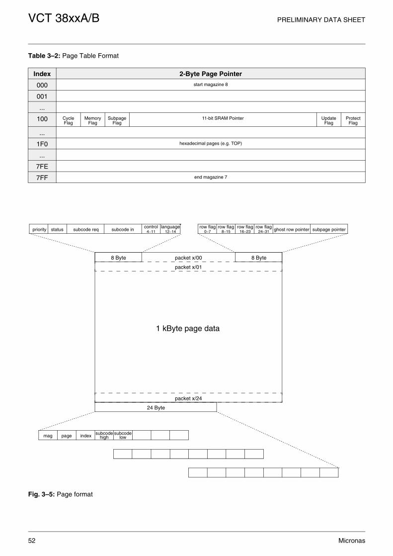
VCT 38xxA/B PRELIMINARY DATA SHEET
52 Micronas
Fig. 3–5: Page format
Table 3–2: Page Table Format
Index 2-Byte Page Pointer
000 start magazine 8
001
...
100 CycleFlag
MemoryFlag
SubpageFlag
11-bit SRAM Pointer UpdateFlag
ProtectFlag
...
1F0 hexadecimal pages (e.g. TOP)
...
7FE
7FF end magazine 7
statuslanguage
12−14control
4−11subcode insubcode reqpriority
subcodehigh
subcodelowindexpagemag
1 kByte page data
row flag0−7
row flag8−15
row flag16−23
row flag24−31 ghost row pointer subpage pointer
8 Byte8 Byte
packet x/01
packet x/24
packet x/00
24 Byte

PRELIMINARY DATA SHEET VCT 38xxA/B
Micronas 53
3.5.4. Ghost Row Organization
Page-related ghost rows are stored in blocks of128 Bytes. These ghost blocks are linked togetherusing 2-Byte ghost row pointers. The first pointer canbe found in the basic page, all following pointers arepart of the block header. A zero pointer indicates theend of the chain.
Fig. 3–6: Ghost row organization
Every ghost block contains 3 ghost rows which can beidentified by 3 row identification bytes in the blockheader. The row identification contains designationcode and row number. The row number is reduced to a3-bit tag. All ghost rows in one block belong to thesame page. If the memory manager removes a pagefrom memory, the linked ghost blocks will also beremoved.
Fig. 3–7: Ghost block structure
ghostpointerPage Table
page 100page pointer
ghostpointer
ghost block
0000
ghost block
Table 3–3: Ghost Row Identification
Row Number Tag Row
000 empty
001 row 25
010 row 26
011 row 27
100 row 28
101 row 29
110 row 30
111 row 31
3-bit row number4-bit designation code
‘aa’ ‘aa’ ‘aa’ row 2row 1 row 3 ghost row pointer
40 Byte row 1 data
40 Byte row 2 data
40 Byte row 3 data
8 Byte block header

VCT 38xxA/B PRELIMINARY DATA SHEET
54 Micronas
3.5.5. Subpage Manager
Any page in cycle can have a number of subpages,identified by subcode. In normal mode the subpagemanager will acquire only one subpage of everyrequested page. This subpage can be any if subcodeFFFF is requested or it will be selected according tothe requested subcode.
After a PAGE_REQUEST command with subcodeF0xx, the subpage manager will acquire all subpagesof the requested page. The subpages will be chainedin the same order as they are transmitted, i.e. everynew subcode will be added at the end of chain. Thepage table entry points to the subpage which wastransmitted first after the page request. TheREAD_PAGE_INFO command will reply the pagetable pointer and the actual number of subpages inchain.
After a PAGE_REQUEST command with subcodeF1xx, the subpage manager will acquire all subpagesof the requested page but will allocate only a limitedamount of memory to store these subpages. Theparameter “page subcode low” will define the length (innumber of subpages) of a ring buffer in page memorywhich will hold the recently received subpages. In thiscase, the READ_PAGE_INFO command will return anindex pointing to the most recently updated subpage inchain, together with the subcode of this page.
The DISPLAY_PAGE_REQUEST command searchesand displays a page according to the requested dis-play subcode. The search starts from page table andcontinues through the subpage chain if there is any. Arolling header will be displayed if the requested sub-page cannot be found in memory.
A requested display subcode FFFF (don’t care sub-code) will only search and display the first subpage inchain, thus there is no rolling subpage anymore. ADISPLAY_PAGE_REQUEST command with subcodeF0xx (follow subcode) will search and display the lastreceived subpage in chain, thus it is possible torequest all subpages in background while still showingrolling subpages in display.
Fig. 3–8: Subpage organization
page 100subcode 0002
0000
page 100subcode 0001
subpagepointer
page 100subcode 0003
subpagepointer
page pointer
Page Table

PRELIMINARY DATA SHEET VCT 38xxA/B
Micronas 55
3.6. WST Display Controller
The display controller reads data from a display pagebuffer in the internal/external SRAM. The display pagebuffer is organized in rows which are separated intolevel 1 data such as character codes and spacingattributes and into level 2 data, such as character setextension and non-spacing attributes. To limit thememory amount for level 2 data, a slightly modifiedstack model is used, in which one pointer bit for everycharacter location indicates the presence of additionalparallel attributes. Fig. 3–9 shows the organization ofthe stack row buffer. In this stack model the number ofnon-spacing attributes per row is limited to 40, whichagrees with the WST and CEPT specification.
Fig. 3–9: Stack Row Buffer
The display controller includes two row buffers. Thefirst row buffer holds a copy of a teletext row from thedisplay page buffer. This decreases the data ratethrough the SRAM interface by a factor of 10 or 8,because new teletext row data is needed only after10 lines in PAL or 8 lines in NTSC mode. The secondrow buffer stores all display attributes in parallel, toallow level 2 display without additional decoding.
To present a WST level 2 display, the teletext displaycontroller has to evaluate the following attributes inparallel, that is for every character location:
– 10-bit character code
– 5-bit foreground color
– 5-bit background color
– 2-bit size
– 5-bit flash
– 1-bit invert
– 1-bit separated
– 1-bit conceal
– 1-bit underline
– 1-bit boxing/window
Additional attributes are defined to improve the displayof CAPTION and OSD text:
– 1-bit italics
– 1-bit shadow
– 1-bit color mode
The display controller delivers 5-bit digital color infor-mation, a shadow signal for contrast reduction, and afast blank signal. The color bus is used to address thecolor look-up table (CLUT) in the video processor. Bythis means, the full level 2 color spectrum can be dis-played.
Level 2 Buffer
1
1
1
1
1
1
1
1
0
0
0
0
0
0
0
0
0
0
0
0
1
1
1
1
0
0
0
0
0
0
Pointer
Char 36 Attr.
Char 38
Char 40
Char 39
Char 36
Char 37
Level 1 Buffer
Char 10 Attr.
Char 1
Char 2
Char 3
Char 4
Char 5
Char 6
Char 7
Char 8
Char 9
Char 10
Char 3 Attr.
Char 3 Attr.
Char 3 Attr.
Char 3 Attr.
Char 6Attr.
Char 6 Attr.
Char 6 Attr.
Char 10 Attr.
Char 10 Attr.

VCT 38xxA/B PRELIMINARY DATA SHEET
56 Micronas
3.7. Display Memory
The TPU supports a variable number of display memo-ries, each 4 kBytes large. One bank is used to storethe display information of the selected teletext page.The bank location can be defined with the command
DISPLAY_TTX_POINTER. Other banks can be usedto store any kind of display data in level 1 or level 2 for-mat. Switching between these banks is fast and can beprogrammed with the command DISPLAY_POINTER.Bank switching allows generation of OSD menus with-out affecting the teletext display.
Fig. 3–10: Display memory organization (level 2)
Display Bank
40 Byte level 1 40 Byte level 2 full row attr.40-bit pointer
40 Byte level 1 40 Byte level 2 full row attr.40-bit pointer
40 Byte level 1 40 Byte level 2 full row attr.40-bit pointer
40 Byte level 1 40 Byte level 2 full row attr.40-bit pointer
40 Byte level 1 40 Byte level 2 full row attr.40-bit pointer
40 Byte level 1 40 Byte level 2 full row attr.40-bit pointer
TTX Display Bank
Row 0
Row 0
Row 1
Row 1
Row 46
Row 25
SRAM
autoincrement

PRELIMINARY DATA SHEET VCT 38xxA/B
Micronas 57
Table 3–5: Full row attribute
+ 55H R/W Full Row Attribute
Bit Reset Function
7 - 1 = row is displayed blank0 = row is displayed using row data
6 - 1 = row is displayed in double height0 = row is displayed in normal height
5 - 1 = row is displayed in level 2 mode0 = row is displayed in level 1 mode
4 to 0 - 5-bit value defining full row background color
Table 3–6: Level 1 spacing attributes
Code Function Action Notes
00 Alpha Black set alpha mode and foreground color of following alpha characters
select character set 0
01 Alpha Red
02 Alpha Green
03 Alpha Yellow
04 Alpha Blue
05 Alpha Magenta
06 Alpha Cyan
07 Alpha White
08 Flash Normal
09 Flash Off set at
0A Boxing Off set at double
0B Boxing On set at double
0C Size Normal set at
0D Size Double Height
0E Size Double Width
0F Size Double
10 Mosaic Black set mosaic mode and foreground color of following mosaic characters
select character set 1
11 Mosaic Red
12 Mosaic Green
13 Mosaic Yellow
14 Mosaic Blue
15 Mosaic Magenta
16 Mosaic Cyan
17 Mosaic White
18 Conceal set at
19 Contiguous Mosaic set at
1A Separated Mosaic set at
1B ESC
1C Black Background set at
1D New Background set at
1E Hold Mosaic set at
1F Release Mosaic
Shaded attributes are default at start of each display row.
Table 3–7: Level 2 parallel attributes
7 6 5 4 3 2 1 0 FunctionP 0 0 Color Foreground Color
P 0 1 Color Background Color
P 1 0 Flash Flash Mode
P 1 1 0 0 L Set Character Set
P 1 1 0 1 0 DH DW Size
P 1 1 0 1 1 0 U Underline/Separated
P 1 1 0 1 1 1 I Inverted
P 1 1 1 0 0 0 C Conceal
P 1 1 1 0 0 1 W Window/Boxing
P 1 1 1 0 1 0 S Shadow
P 1 1 1 0 1 1 IT Italic
P 1 1 1 1 0 0 CM Color Mode
Table 3–8: Color look-up table
4 3 2 1 0 Display Color0 0 0 0 0 Black
0 0 0 0 1 Red
0 0 0 1 0 Green
0 0 0 1 1 Yellow
0 0 1 0 0 Blue
0 0 1 0 1 Magenta
0 0 1 1 0 Cyan
0 0 1 1 1 White
0 1 0 0 0 Transparent
0 1 0 0 1 Reduced Red
0 1 0 1 0 Reduced Green
0 1 0 1 1 Reduced Yellow
0 1 1 0 0 Reduced Blue
0 1 1 0 1 Reduced Magenta
0 1 1 1 0 Reduced Cyan
0 1 1 1 1 Reduced White
1 x x x x Programmable
Table 3–4: Flash modes
4 3 2 1 0 Function0 0 0 0 0 Off
0 0 0 0 1 Normal
0 0 1 0 1 Normal Fast Phase 1
0 1 0 0 1 Normal Fast Phase 2
0 1 1 0 1 Normal Fast Phase 3
0 0 0 1 0 Inverted
0 0 1 1 0 Inverted Fast Phase 1
0 1 0 1 0 Inverted Fast Phase 2
0 1 1 1 0 Inverted Fast Phase 3
0 0 0 1 1 Color Table
0 0 1 1 1 Color Table Phase 1
0 1 0 1 1 Color Table Phase 2
0 1 1 1 1 Color Table Phase 3
1 0 0 x x Incremental
1 0 1 x x Decremental

VCT 38xxA/B PRELIMINARY DATA SHEET
58 Micronas
3.8. Character Generator
Characters are addressed using a 10-bit charactercode. The 2 MSBs of the character code define 1 of 4character sets. Character set selection is done usinglevel 2 parallel attributes (see Table 3–7 on page 57).Each character set contains 224 characters. The first32 characters in each character set are reserved forcontrol codes (see Table 3–6 on page 57). On a singlescreen, 896 different characters can be displayed.
Characters can be displayed in several pixel resolu-tions provided that the according font is available. Thecharacter generator supports horizontal resolution of8 or 10 pixel/char and vertical resolution of 8, 10, or13 lines/char. Characters can be combined withoutseparating borders to create more complex characterdefinitions (e.g. kanji or icons).
The pixel clock can be either 10.125 MHz or20.25 MHz. To get 10-bit pixel information from thecharacter font, two memory cycles are needed. Thecharacter font is part of the mask-programmable ROM,but supplied with its own bus structure (see Fig. 3–2on page 50). By this means the data transfer betweencharacter ROM and teletext display controller does notstop the CPU.
Both bus structures are connected via a memory inter-face which allows cross-connections using DMA orwait cycles. If the character font size exceeds12 kBytes, part of the character font can be shifted intothe program ROM which causes DMA cycles. There-fore only less frequently used characters should beplaced into the program ROM. Vice versa seldom usedCPU code can be put into the character ROM.
The WST specification defines a number of 7-bit codetables, which are filled with 96 characters only (theMSB is used for parity check). In the G0 code tablesome characters have several language dependentvariations. Additionally characters from the G0 codetable can be combined with diacritical marks from theG2 code table (row 26). Furthermore different codetables are defined for languages like cyrillic, greek orarabic. Thus it is not possible to simply transform thecode tables into a continuous character font ROMwithout getting unused ROM space and multipledefined character fonts.
This problem is solved by implementing a charactercode mapping (see Fig. 3–11 on page 59). The5 MSBs of each character code are mapped intoanother 5-bit code which is then used to address thecharacter font ROM. By this means the whole charac-ter font is subdivided into 32 blocks of 32 characterswhich can freely be distributed over the 4 charactersets.
The character code mapping is implemented as RAMand can be programmed by software. After reset theTPU initializes the mapping RAM for standard WSTlatin code tables.
The TV controller can select predefined mappings forlatin, cyrillic and arabic teletext via the commandDISPLAY_MODE (see Table 3–16 on page 72). Thesame command allows selection of a user definedmapping which has to programmed in advance usingcommand USER_MAPPING.
Table 3–9: Character resolutions
matrix(h x v)
char/screen(PAL)
char/screen(NTSC)
osd width
# char in 12k font
# char in 24k font
single character
8 x 8 40 x 32 40 x 28 32µs 1600 3072
10 x 8 40 x 32 40 x 28 40µs 1280 2458
8 x 10 40 x 26 40 x 22 32µs 1280 2458
10 x 10 40 x 26 40 x 22 40µs 1024 1966
8 x 13 40 x 20 40 x 17 32µs 800 1536
10 x 13 40 x 20 40 x 17 40µs 640 1229
combined character (2 x 2)
16 x 16 20 x 16 20 x 14 32µs 400 768
20 x 16 20 x 16 20 x 14 40µs 320 614
16 x 20 20 x 13 20 x 11 32µs 320 614
20 x 20 20 x 13 20 x 11 40µs 256 492
16 x 26 20 x 10 20 x 8.5 32µs 200 384
20 x 26 20 x 10 20 x 8.5 40µs 160 307
combined character (2 x 1)
16 x 10 20 x 26 20 x 22 32µs 640 1229
16 x 13 20 x 20 20 x 17 32µs 400 768
20 x 13 20 x 20 20 x 17 40µs 320 614
combined character (1x 2)
10 x 16 40 x 16 40 x 14 40µs 640 1229

PRELIMINARY DATA SHEET VCT 38xxA/B
Micronas 59
3.8.1. Character Code Mapping
Fig. 3–11: Character code mapping
Character Set 0
G2
National
National
National
National
National
National
National
National
10-bit Character Code = 2-bit Character Set (level 2) + 8-bit Character Value (level 1)
000H
080H
100H
180H
200H
280H
300H
G3
G3
G3
User
User
User
User
380H
Mapping RAM32 x 5 bit
G2
G2
G2
User
User
User
User
G1
G0
G1
User
User
User
G3
G3
12800 Byte
Character ROM
G2
G2
User
G1
National
G1
National
National
G0
G0
G0
National
G0
G0
G0
block of 32 char
G3
Greek
Greek
Cyrillic
Cyrillic
Cyrillic
Hebrew
Arabic
Arabic
Arabic
00
01
02
03
04
05
06
07
08
09
10
11
12
13
14
15
16
17
18
19
20
21
22
23
24
25
26
27
28
29
30
31
Character Set 1
Character Set 2
Character Set 3
08
09
10
11
12
13
14
15
00
01
02
03
04
05
06
07
16
17
18
19
20
21
22
23
24
25
26
27
28
29
30
31
Font Pointer
Farsi

VCT 38xxA/B PRELIMINARY DATA SHEET
60 Micronas
3.8.2. Character Font ROM
The character font ROM is mask-programmable.Design of customer specific characters (user font) issupported by a Windows™ based PC tool namedMOFA (Micronas OSD and Font Assembler). In combi-
nation with the VCT 38xxA/B emulator board it is pos-sible to download character fonts and verify them onthe TV screen.
Fig. 3–12: Character font ROM for Teletext

PRELIMINARY DATA SHEET VCT 38xxA/B
Micronas 61
3.8.3. Latin Font Mapping
Fig. 3–13: Latin font mapping

VCT 38xxA/B PRELIMINARY DATA SHEET
62 Micronas
3.8.4. Cyrillic Font Mapping
Fig. 3–14: Cyrillic font mapping

PRELIMINARY DATA SHEET VCT 38xxA/B
Micronas 63
3.8.5. Arabic Font Mapping
Fig. 3–15: Arabic font mapping

VCT 38xxA/B PRELIMINARY DATA SHEET
64 Micronas
3.8.6. Closed Caption Font (on VCT 38xxB only!)
Fig. 3–16: Character font ROM for Closed Caption
Fig. 3–17: Closed Caption font mapping

PRELIMINARY DATA SHEET VCT 38xxA/B
Micronas 65
3.8.7. Character Font Structure
Fig. 3–18: Font Structure 10 x 10
Fig. 3–19: Font structure 8 x 13
Line 1Line 2Line 3Line 4Line 5Line 6Line 7Line 8Line 9Line 10
Line 1Line 2Line 3Line 4Line 5Line 6Line 7Line 8Line 9Line 10Line 1Line 2Line 3Line 4
‘@‘‘@‘‘@‘‘@‘‘@‘‘@‘‘@‘‘@‘‘@‘‘@‘‘A‘‘A‘‘A‘‘A‘
Character Font
‘A‘‘A‘‘A‘‘A‘‘A‘‘A‘‘A‘‘A‘‘A‘‘A‘‘E‘‘E‘‘E‘‘E‘
‘B‘‘B‘‘B‘‘B‘‘B‘‘B‘‘B‘‘B‘‘B‘‘B‘‘F‘‘F‘‘F‘‘F‘
‘@‘‘@‘
‘@‘
‘@‘‘@‘
‘@‘
‘@‘
‘@‘‘@‘
‘@‘
‘D‘‘D‘
‘D‘
‘D‘
‘C‘‘C‘‘C‘‘C‘‘C‘‘C‘‘C‘‘C‘‘C‘‘C‘‘G‘‘G‘‘G‘‘G‘
Extension Font
Line 1Line 2Line 3Line 4Line 5Line 6Line 7Line 8Line 9Line 10Line 1Line 2Line 3Line 4
LSBMSB09
Line 1Line 2Line 3Line 4Line 5Line 6Line 7Line 8Line 9Line 10
Line 1Line 2Line 3Line 4Line 5Line 6Line 7Line 8Line 9Line 10Line 11Line 12Line 13Line 14
‘P‘‘P‘‘P‘‘P‘‘P‘‘P‘‘P‘‘P‘‘P‘‘P‘
‘Q‘‘Q‘‘Q‘
Character Font
LSBMSB07
Line 11Line 12
Line 13
Line 15Line 16
Line 1
Line 2Line 3
‘P‘‘P‘‘P‘

VCT 38xxA/B PRELIMINARY DATA SHEET
66 Micronas
3.9. National Character Mapping
Table 3–10: Character set options
Option Bits
C14,C13,C12
Character Set
6 38 40 55 70 128
000 English Polish English (US) English English (US) programmable
001 French French French French Slovakian programmable
010 Swedish Swedish Swedish Swedish Hungarian programmable
011 Czech Czech Czech Turkish Serbian programmable
100 German German German German Albanian programmable
101 Spanish Serbian Spanish Spanish Polish programmable
110 Italian Italian Italian Italian Turkish programmable
111 Estonian Estonian Estonian Estonian Rumanian programmable
Table 3–11: Language codes
Code Language
0 English
1 French
2 Swedish, Finnish
3 Czech
4 German
5 Spanish
6 Italian
7 Estonian, Finnish
8 English (US)
9 Slovakian
10 Hungarian
11 Serbian, Croatian, Slovene
12 Albanian
13 Polish
14 Turkish
15 Rumanian
16 Cyrillic (Russian, Bulgarian)
17 Greek
18 Cyrillic (Serbian, Montenegro)
19 YU Latin
20 Arabic
21 Hebrew
22 Farsi
23 Lettish, Lithuanian
24 Cyrillic (Ukrainian)
25−255 not defined

PRELIMINARY DATA SHEET VCT 38xxA/B
Micronas 67
Table 3–12: National option mapping
Language G0/G1 Table Position
2/3 2/4 4/0 5/11 5/12 5/13 5/14 5/15 6/0 7/11 7/12 7/13 7/14
Albanian 5/15 2/4 13/12 13/2 12/12 12/3 11/12 9/1 13/13 13/3 12/13 13/1 11/13
Czech 5/15 12/9 13/13 10/11 12/13 12/11 8/4 15/13 9/3 8/3 12/0 9/2 11/13
English 2/3 2/4 4/0 5/11 5/12 5/13 5/14 5/15 6/0 7/11 7/12 7/13 7/14
English (US) 5/15 2/4 4/0 14/4 13/5 15/4 14/6 13/0 14/7 14/5 15/6 15/5 15/7
Estonian, Finnish 5/15 11/11 11/12 8/13 8/14 12/12 8/15 11/10 11/13 8/10 8/11 12/13 8/12
French 9/3 8/1 8/5 9/1 9/7 8/2 8/8 5/15 9/5 8/7 9/8 8/9 9/0
German 5/15 2/4 15/0 8/13 8/14 8/15 14/6 13/0 14/0 8/10 8/11 8/12 9/10
Hungarian 5/15 9/2 9/14 8/4 8/14 10/1 12/15 11/15 9/3 9/4 8/11 8/3 8/12
Italian 2/3 2/4 9/3 14/0 9/0 5/13 5/14 5/15 8/2 8/5 9/6 9/5 8/6
Polish 5/15 14/3 13/15 13/8 12/7 15/8 13/3 9/4 10/9 13/9 13/7 15/9 13/11
Rumanian 5/15 14/1 10/14 10/5 14/14 14/11 10/6 15/1 10/15 8/7 14/15 12/5 8/8
Serbian, Croatian 5/15 2/4 13/12 13/2 12/12 12/3 11/12 13/0 13/13 13/3 12/13 13/1 11/13
Slovakian 5/15 12/9 13/13 10/11 12/13 12/11 8/4 15/13 9/3 8/3 12/0 9/2 11/13
Spanish 9/0 2/4 9/15 8/3 9/3 8/4 9/4 9/2 9/9 8/12 9/11 9/5 8/5
Swedish, Finnish 5/15 14/1 9/14 8/13 8/14 9/13 8/15 13/0 9/3 8/10 8/11 9/12 8/12
Turkish 13/6 10/13 10/8 14/14 8/14 8/0 8/15 10/12 15/1 14/15 8/11 9/0 8/12
YU Latin 5/15 2/4 13/12 13/2 12/12 12/3 11/12 13/0 13/13 13/3 12/13 13/1 11/13

VCT 38xxA/B PRELIMINARY DATA SHEET
68 Micronas
3.10. Four-Color Mode
In “Four-Color Mode” the color depth of single or multi-ple characters can be increased to 4 colors (e.g. to dis-play icons or 3-D effects). A special font organization isrequired because two consecutive characters will becombined. The number of 4-colored characters is onlylimited by font size.
The “Four-Color Mode” is controlled via the level 2 par-allel attribute “Color Mode”. Setting the bit CM to 1activates the “Four-Color Mode” until the end of row oruntil the bit CM is set to 0 again. At the start of eachdisplay row the “Four-Color Mode” is disabled.
A character with active “Four-Color Mode” attribute willbe combined with its font neighbor to define a 2bit/pixel character matrix. The 2 additional colors arederived from the active foreground and backgroundcolors by inverting bit 3 of the color code. Using theprogrammable part of the CLUT it is possible to displaycharacters in 4 out of 4096 colors.
If the “Four-Color Mode” attribute is set for a characterwith even character code n, this character is combinedwith its font neighbor addressed by code n + 1. If the“Four-Color Mode” attribute is set for a character withodd character code, this character is combined withitself.
The neighbor character does not change the definitionof foreground and background pixel which is used tocontrol flash and mix mode.
Fig. 3–20: Four-color mode
Table 3–13: Color Allocation
Pixel Definition Color Allocation
Character n
Character n+1
0 0 background
1 0 foreground
0 1 background .xor. 8
1 1 foreground .xor. 8
Matrix of Character n Matrix of Character n+1 4 Color Display
+ =
00 10
01 11

PRELIMINARY DATA SHEET VCT 38xxA/B
Micronas 69
3.11. OSD Layer
Apart from the WST layer, there is an additional OSDlayer on chip. The OSD layer accesses the CPU mem-ory via DMA to read text, display attributes, and char-acter font information. The color outputs of the OSDlayer can have higher priority than the WST layer out-puts. Thus, it is possible to overlay the teletext displaywith an additional layer for user guidance (see Fig. 3–21).
Fig. 3–21: Display layer
The OSD layer reads text strings addressed by a pro-grammable text pointer. Codes smaller than 80h willaddress the character font, codes greater or equal 80hare interpreted as control codes to change color orcharacter set (see Table 3–14). After reading a controlcode the OSD layer will do an additional read to getthe next character code.
OSD Layer
WST Layer
Full Screen Layer
Table 3–14: OSD Layer Control Codes
Code Function Notes
01 Underline On only for 13 scanlines/character
02 Underline Off
03 Flash On
04 Flash Off
05 Italics On
06 Italics Off
07 Transparent layer becomes transparent
08 Shadow layer becomes transparent and contrast is reduced to 66%
0C END end of layer
0D CR end of text line
0E − 7F ASCII Character using font 1 or font 2
80 − FF Control Code Only one control code per character is allowed. Depending on OSD Mode, the control code defines either color or character set.
Color bit 0 = foreground color bluebit 1 = foreground color greenbit 2 = foreground color redbit 3 = background color bluebit 4 = background color greenbit 5 = background color redbit 6 = replace white by transparentbit 7 = 1
Character Set bit 0 = bit 7 of character codebit 1 = bit 8 of character codebit 2 = bit 9 of character codebit 3 = bit 4 = bit 5 = bit 6 = latching shift to character setbit 7 = 1
Shaded attributes are default at start of each text line.

VCT 38xxA/B PRELIMINARY DATA SHEET
70 Micronas
3.12. Command Language
The TPU supports a command language, allowing theTV controller to start complex processing inside theTPU with simple commands. The TV controller is notburdened with time consuming tasks like page search-ing or data shuffling.
Table 3–15 lists all available commands. For a moredetailed description of the command language seeTable 3–16.
The application software has to send commands to theTPU via I2C bus using the command subaddressSUB4 (see Section 3.14.1.3. on page 86).
Table 3–15: Command language cross reference
Code Dec. Code Hex. Command Name No. Write Parameter
No. Read Parameter
Status Register
0 00 Dummy 0 0 x000 0000
1 01 Reset 0 0 x000 0000
2 02 Escape 0 0 x000 0000
3 03 Version 0 2 x000 0000
4 04 Test 0 0 x000 0000
5 05 Test 0 0 x000 0000
6 06 DRAM Mode 3 0 x000 0000
7 07 Acquisition Mode 6 2 x000 0000
8 08 Display Mode 3 0 x000 0000
9 09 Display TTX Pointer 2 0 x000 0000
10 0a Display Pointer 3 0 x000 0000
11 0b Display Clear 2 0 x000 0000
12 0c Page Request 8 3 x0x0 0000
13 0d Display Time Pointer 2 0 x000 0000
14 0e Read DRAM Size 0 3 x000 0000
15 0f Read VPS 0 15 x0x0 0000
16 10 Read Quality 0 6 x000 0000
17 11 Read Display Mode 0 3 x000 0000
18 12 Read Reset Source 0 1 x000 0000
19 13 Read Rolling Header 0 24 x000 0000
20 14 Read Page Info 2 7 x000 0000
21 15 Read Page Row 5 40 x0x0 0000
22 16 Change Page Info 3 0 x000 0000
23 17 Search MPET 0 1 + (n*4) x0x0 0000
24 18 Read Display Page 0 4 x000 0000
25 19 Page Memory 2 0 x000 0000
26 1a Display Page Request 5 0 x000 0000
27 1b Page Table Reset 0 0 x000 0000
28 1c Search Next Page 3 6 x0x0 0000
29 1d Read Page Cycle 0 9 x000 0000
30 1e Read TOP Code 2 2 x000 0000
31 1f Read Rolling Time 0 8 x000 0000
32 20 Copy Page Row 8 0 x0x0 0000
33 21 Copy Data 7 0 x000 0000
34 22 Search Next TOP Code 3 4 x0x0 0000
35 23 Read Ghost Row 6 40 x0x0 0000

PRELIMINARY DATA SHEET VCT 38xxA/B
Micronas 71
36 24 Read 8/30 Row 1 40 x0x0 0000
37 25 Read Priority 0 5 x000 0000
38 26 Page Priority 2 0 x000 0000
39 27 Search AIT 0 1 + (n*4) x0x0 0000
40 28 Read TOP Status 0 2 x000 0000
41 29 Search AIT Title 2 17 x0x0 0000
42 2a Reset Ghost Row Status 0 0 x000 0000
43 2b Search MPT 0 1 + (n*4) x0x0 0000
44 2c Copy AIT Title 5 17 x0x0 0000
45 2d Search Direct Choice 1 1 + (n*2) x0x0 0000
46 2e Read Hamming 1 1 x000 0000
47 2f Read Hamming 2 3 3 x000 0000
48 30 Display Column 3+length 0 x000 0000
49 31 Display Fill 4 0 x000 0000
50 32 Read BTTL 0 9 x0x0 0000
51 33 Read Next Page 2 2 x000 0000
52 34 Change BTT magazine 1 0 x000 0000
53 35 Read WSS 0 15 x0x0 0000
54 36 Read CAPTION 1 0 7 x0x0 0000
55 37 Read CAPTION 2 0 7 x0x0 0000
56 38 Display Font Pointer 5/1/3 0 x000 0000
57 39 Display Read Column 3 length x000 0000
58 3a User Character Set 8 0 x000 0000
59 3b User ESC Character Set 8 0 x000 0000
60 3c Full Row Attribute 3 0 x000 0000
61 3d User Mapping 32 0 x000 0000
62 3e Execute Code on Stack 0 0 x000 0000
63 3f Disable Ghost Rows 1 0 x000 0000
Table 3–15: Command language cross reference, continued
Code Dec. Code Hex. Command Name No. Write Parameter
No. Read Parameter
Status Register

VCT 38xxA/B PRELIMINARY DATA SHEET
72 Micronas
Note:If not otherwise designated, all parameters in the following table are specified as single bytes. As writeparameter magazine numbers 8 and 0 have the same meaning, as read parameter the magazine number is atrue 4-bit number (e.g. magazine 8= 00001000). For write parameters the values in parentheses indicatedefault values after reset (in hex notation). For compatibility reasons every undefined bit in a write parame-ter should be set to ‘0’. Undefined bits in a read parameter should be treated as “don’t care”.
Table 3–16: Command language
Code Function Write Parameter Read Parameter Notes
Operational & Test Commands
00 Dummy no action
01 Reset software reset of 65C02
02 Escape escape to other codes
03 Version CPU pointer highCPU pointer low
show version in OSD layerCPU pointer to text in ROM
04 Test reserved for testing
05 Test reserved for testing
06 DRAM Mode dram mode (06)flash inc (05)control enable (FF)
dram mode = I/O page register 028EHflash freq = flash inc / (256 * 0.00324)control enable:
bit0 = C4 erase pagebit1 = C5 news flashbit2 = C6 subtitlebit3 = C7 suppress headerbit4 = C8 update indicatorbit5 = C9 interrupted sequencebit6 = C10 inhibit displaybit7 = C11 magazine parallel
07 Acquisition Mode acquisition mode (00)init subcode high (FF)init subcode low (FF)gain max (1F)filter max (1F)acq. sync slicer (19)
gainfilter
acquisition mode:bit0 = no slicer adaptionbit1 = no bit error in framing codebit2 = limit slicer adaptionbit3 = acq. sync slicer
init subcode:automatic subcode request afterpage table reset
gain max: only used if bit2 = 1filter max: only used if bit2 = 1acq. sync slicer: only used if bit3 = 1
62 Execute Code on Stack execute “JSR 0x100”
Memory Management Commands
14 Read DRAM Size dram size highdram size lowdram mode
dram size:000CH = 3 kByte SRAM004CH = 19 kByte SRAM0200H = 128 kByte SRAM0240H = 144 kByte SRAM0400H = 256 kByte SRAM0800H = 512 kByte SRAM
dram mode:see I/O page register 028EH
25 Page Memory dram bank (00)dram high (40)
start of page memoryexecute page table reset
27 Page Table Reset reset page tablereset ghost row statusreset data service statusreset cycle countreset memory countreset ghost countreset prioritiesclear rolling headerclear VPS dataclear WSS data

PRELIMINARY DATA SHEET VCT 38xxA/B
Micronas 73
42 Reset Ghost Row Status ghost row status:bit0 = row 24 in cyclebit1 = row 25 in cyclebit2 = row 26 in cyclebit3 = row 27 in cyclebit4 = row 28 in cyclebit5 = row 29 in cyclebit6 = row 30 in cyclebit7 = row 31 in cycle
63 Disable Ghost Rows ghost row disable ghost row disable:bit0 = disable row 24 acquisitionbit1 = disable row 25 acquisitionbit2 = disable row 26 acquisitionbit3 = disable row 27 acquisitionbit4 = disable row 28 acquisitionbit5 = disable row 29 acquisitionbit6 = disable row 30 acquisitionbit7 = disable row 31 acquisition
29 Read Page Cycle ghost row status2 Byte cycle count2 Byte memory count2 Byte ghost countdata service statusmemory status
= number of pages in cycle= number of pages in memory= number of ghost blocks in memorydata service status:
bit0 = 8/30 format 1 updatedbit1 = 8/30 format 2 updatedbit2 = VPS updatedbit3 = WSS updatedbit4 = CAPTION 1st field updatedbit5 = CAPTION 2nd field updated
memory status:bit0 = memory full
38 Page Priority enable (00)border (FF)
enable:bit0 = enable priority manager
border:min/max border for page priorities
37 Read Priority highest prioritylowest priorityborder prioritymagazine numberpage number
= max priority in page memory = min priority in page memory = min/max border for page priorities = page with lowest priority
Page Related Commands
12 Page Request magazine numberpage numberpage subcode highpage subcode lowpriorityquantitystart magazine numberstart page number
number of open requestsremoved magazine numberremoved page number
remove pages from memory beginning at start page if page priority is disabled, ignores start page if page priority is enabledmagazine number:
bit0−3 = magazine numberbit4 = not usedbit5 = hex requestbit6 = backward requestbit7 = forced request
= ignore cycle flag
20 Read Page Info magazine numberpage number
page pointer highpage pointer lowsubpage countghost row countring buffer indexpage subcode highpage subcode low
= pointer from page table
= number of subpages in chain= number of ghost rows in chainif page request with subcode F1xx
22 Change Page Info magazine numberpage numberpage table flags
page table flags:bit0 = protectionbit1 = updatebit2 = not usedbit3 = not usedbit4 = not usedbit5 = subpagebit6 = memorybit7 = cycle
Table 3–16: Command language, continued
Code Function Write Parameter Read Parameter Notes

VCT 38xxA/B PRELIMINARY DATA SHEET
74 Micronas
28 Search Next Page magazine numberpage numbersearch code
magazine numberpage numberpage pointer highpage pointer lowsubpage countghost row count
search in page table for cycle flagmagazine number:
bit0−3 = magazine numberbit4 = take search codebit5 = hex searchbit6 = backward searchbit7 = include start page
search code:bit0 = search protection flagbit1 = search update flagbit2−4 = not usedbit5 = search subpage flagbit6 = search memory flagbit7 = search cycle flag
51 Read Next Page magazine numberpage number
magazine numberpage number
calculate next page numbermagazine number:
bit0−3 = magazine numberbit4 = not usedbit5 = hex calculationbit6 = backward calculationbit7 = not used
21 Read Page Row magazine numberpage numbersubpage number highsubpage number lowrow number
40 Byte row data row 0 − 24
32 Copy Page Row magazine numberpage numbersubpage number highsubpage number lowrow numberdestination dram bankdestination dram highdestination dram low
copy 40Byte text row from page memory into DRAM
35 Read Ghost Row magazine numberpage numbersubpage number highsubpage number lowrow numberdesignation code
40 Byte row data row 25 − 28
TOP Commands
40 Read TOP Status TOP status 1TOP status 2
TOP status 1:bit0 = not usedbit1 = MPT link in PLTbit2 = MPET link in PLTbit3 = AIT link in PLTbit4 = BTT in memorybit5 = MPT in memorybit6 = MPET in memorybit7 = AIT in memory
TOP status 2:bit0−5 = not usedbit6 = all MPET in memorybit7 = all AIT in memory
30 Read TOP Code magazine numberpage number
BTT codeMPT code
code:bit0−3 = databit6 = hamming error
50 Read BTTL BTTL error8 Byte BTTL data
BTTL error:bit6 = hamming error in BTTL
BTTL data:bit0−3 = databit6 = hamming error
52 Change BTT magazine magazine number (01) all TOP commands then refer to this magazine
43 Search MPT number of MPTsmagazine numberpage numbersubpage number highsubpage number low...
search in PLT
Table 3–16: Command language, continued
Code Function Write Parameter Read Parameter Notes

PRELIMINARY DATA SHEET VCT 38xxA/B
Micronas 75
23 Search MPET number of MPETsmagazine numberpage numbersubpage number highsubpage number low...
search in PLT
39 Search AIT number of AITsmagazine numberpage numbersubpage number highsubpage number low...
search in PLT
41 Search AIT Title magazine numberpage number
5 Byte data12 Byte title
search in AITmagazine number:
bit0−3 = magazine number (0#8)bit4−6 = not usedbit7 = ignore title language
data:bit0−3 = databit6 = hamming error
44 Copy AIT Title magazine numberpage numberdestination dram bankdestination dram highdestination dram low
5 Byte data12 Byte title
search in AIT and copy title into drammagazine number:
bit0−3 = magazine number (0#8)bit4−6 = not usedbit7 = ignore title language
data:bit0−3 = databit6 = hamming error
34 Search Next TOP Code magazine numberpage numbercode condition
magazine numberpage numbercodecode flag
search in BTTmagazine number:
bit0−3 = magazine numberbit4−5 = not usedbit6 = backward searchbit7 = include start page
code condition:low nibble = BTT codehigh nibble = search condition
0 = BTT code in low nibble1 = BTT code # 02 = block page3 = group page4 = normal page5 = subtitle page6 = TV page7 = block/TV page8 = group/block/TV page9 = subpagea = block/TV subpageb = group/block/TV subpagec = title paged = future pagee = future pagef = future page
code:bit0−3 = BTT codebit6 = hamming error
code flag:bit0 = subtitle page foundbit1 = TV page foundbit2 = block page foundbit3 = group page foundbit4 = normal page foundbit5 = future page foundbit6 = title page foundbit7 = subpage found
45 Search Direct Choice direct choice code number of AIT entriesmagazine numberpage number...
search in AIT
Table 3–16: Command language, continued
Code Function Write Parameter Read Parameter Notes

VCT 38xxA/B PRELIMINARY DATA SHEET
76 Micronas
Miscellaneous Data Commands
36 Read 8/30 Row designation code 40 Byte row data only format 1 and 2 are supported1st byte of row data is already hamming decoded
15 Read VPS framing codecounter13 Byte VPS data
= 51H= incremented every VPS reception= biphase decoded VPS bytes 3−15
53 Read WSS framing codecounter13 Byte WSS data
= 78H= incremented every WSS reception= 102 WSS elements from group 1 on
54 Read CAPTION 1 counter6 Byte CAPTION data
= incremented every reception in field 1= 3x oversampling
55 Read CAPTION 2 counter6 Byte CAPTION data
= incremented every reception in field 2= 3x oversampling
19 Read Rolling Header 24 Byte rolling header every row 0 in cycle
31 Read Rolling Time 8 Byte rolling time using time pointer
16 Read Quality text lineshamming errorsparity errorssoft errorsio_acq_hsync_counterio_acq_sync_status
updated every VBI
18 Read Reset Source reset source reset source:bit0 = clock supervisionbit1 = voltage supervisionbit2 = watchdog
all bits in reset source are reset after read
46 Read Hamming hamming (8,4) Byte data hamming Byte:bit0−3 = databit6 = hamming error
47 Read Hamming 2 hamming (24,18) 1st Bytehamming (24,18) 2nd Bytehamming (24,18) 3rd Byte
addressmodedata
address:bit0−5 = addressbit7 = hamming error
mode:bit0−4 = mode
data:bit0−6 = data
33 Copy Data source dram banksource dram highsource dram lowlengthdestination dram bankdestination dram highdestination dram low
copy data from DRAM to DRAM
Display Commands
17 Read Display Mode display modecharacter setfont mapping
display mode:bit0 = forced boxingbit1 = revealbit2 = boxbit3 = time holdbit4 = page holdbit5 = row 24 holdbit6 = row 25 holdbit7 = row 26 hold
08 Display Mode display mode (18)character set (06)font mapping (00)
display mode: see abovecharacter set: 6,38,40,55,70,128font mapping: 0=latin
1=cyrillic/greek2=arabic/farsi/hebrew128=user defined
09 Display TTX Pointer dram high (20)dram low (00)
page memory is copied to TTX pointer
10 Display Pointer dram high (20)dram low (00)scroll counter (00)
display starts at pointer using scroll counter as line offset
Table 3–16: Command language, continued
Code Function Write Parameter Read Parameter Notes

PRELIMINARY DATA SHEET VCT 38xxA/B
Micronas 77
11 Display Clear dram highdram low
clear display bank beginning at pointer (26 rows * 86 Bytes)
13 Display Time Pointer dram high (20)dram low (20)
8 Byte time string from packet x/00 is copied to time pointer
26 Display Page Request magazine numberpage numbersubpage number highsubpage number lowdisplay delay (1E)
magazine number:bit0−3 = magazine numberbit4 = change display delaybit5 = display clear (on update)bit6−7 = not used
subpage number:F0xx for rolling subpages
display delay:delay after row 0 reception in stepsof 3.24ms (255 = no update)only used if bit4 = 1
24 Read Display Page magazine numberpage numbersubpage number highsubpage number low
current page in display
48 Display Column dram highdram lowlengthByte list...
write to dram with increment of 86 Bytes
= number of bytes in list
49 Display Fill dram highdram lowlengthcharacter
repeated write of 1 character to dram
= number of repeated writes
56 Display Font Pointer font mode (00)
for font mode=1 or 2:font pointer highfont pointer lowextension font pointer highextension font pointer low
font mode:1 = write OSD font 2 pointer2 = write WST font 1 pointer
for font mode=0 font mode:0 = reset OSD font 2 pointer
OSD font pointer = WST font pointer
for font mode=3 or 4:display mode 1display mode 2
font mode:3 = select VCTB 10x13 font4 = select VCTB 10x10 font
57 Display Read Column dram highdram lowlength
Byte list...
read from dram with increment of 86 Bytes= number of Bytes to read
58 User Character Set language 000 (00)language 001 (01)language 010 (02)language 011 (03)language 100 (04)language 101 (05)language 110 (06)language 111 (07)
If character set 128 is selected via command 08 “Display Mode”, these 8 languages will be selected by option bits C14,C13,C12 when ESC code is inactive.
59 User ESC Character Set esc language 000 (00)esc language 001 (00)esc language 010 (00)esc language 011 (00)esc language 100 (00)esc language 101 (00)esc language 110 (00)esc language 111 (00)
If character set 128 is selected via command 08 “Display Mode”, these 8 languages will be selected by option bits C14,C13,C12 when ESC code is active.
60 Full Row Attribute full row attributenumber of rowsstart row
set full row attribute of specified rows without changing level 2 bit
61 User Mapping 32 Byte mapping data 32 Bytes are copied into mapping ram via I/O page register 0276H
Table 3–16: Command language, continued
Code Function Write Parameter Read Parameter Notes

VCT 38xxA/B PRELIMINARY DATA SHEET
78 Micronas
3.13. I/O Register
Most hardware-related functions of the TPU are con-trolled by memory mapped I/O of the 65C02. Theapplication software has access to the I/O registers viaI2C bus using the CPU subaddresses SUB1 and SUB2(see Section 3.14.1.1. on page 86).
Most of the I/O registers can only be written and willnot return useful data when read by application soft-ware. Reset values are written by TPU during initializa-tion.
Note:For compatibility reasons, every undefined bit of awrite register should be set to ‘0’. Undefined bits ofa read register should be treated as “don’t care”.
0200 H R/W CONTROL REGISTER
Bit Reset Write Function Read Function
all 00 H During reset the control register is loaded with the contents of the address FFF9H, but it can be read and written via software.
7 0 1 = CPU disable0 = CPU enable
6 0 1 = program RAM disable0 = program RAM enable
5 0 1 = program ROM disable0 = program ROM enable
4 0 1 = character ROM disable0 = character ROM enable
3 0 1 = DMA interface disable0 = DMA interface enable
2 0 1 = I/O page disable0 = I/O page enable
1 0 1 = test mode on0 = test mode off
0 0 1 = burn-in test mode (only if test pin high)0 = normal test mode
1 = burn-in test mode0 = normal test mode
0202 H Write STANDBY
Bit Reset Function
2 0 1 = digital circuitry power off(CPU still active with slow clock)0 = digital circuitry power on
0213 H Write INTERFACE MODE
Bit Reset Function
1 0 1 = standby enable (if bit 2 of register 0202H = 1)0 = standby disable
0251 H Write BLANKING STOP
Bit Reset Function
all 07 H horizontal stop of blanking pulse in character incrementscorrect blanking pulse cannot be guaranteed if blanking start = blanking stop
0252 H Write BLANKING START
Bit Reset Function
all 00 H horizontal start of blanking pulse or self-timed HSYNC in character incrementscorrect blanking pulse cannot be guaranteed if blanking start = blanking stop

PRELIMINARY DATA SHEET VCT 38xxA/B
Micronas 79
0254 H Write DISPLAY MODE 1
Bit Reset Function
7 0 1 = OSD layer always uses FONT 10 = OSD layer changes from FONT 1 to FONT 2 if ASCII≥20H
6 1 1 = enable OSD layer0 = disable OSD layer
5 1 1 = active flash phase of OSD layer0 = inactive flash phase of OSD layer
4 0 1 = 13 scanlines/character0 = 8 scanlines/character
3 to 0 0 With this scan line the OSD layer starts display of the first text line. By slow incrementing of this value soft scroll begins.
0255 H Write DISPLAY MODE 2
Bit Reset Function
7 0 1 = OSD layer control code defines character set0 = OSD layer control code defines color
3 1 1 = 10.125MHz display clock0 = 20.25MHz display clock
2 1 1 = font pointer offset 10 scanlines/character0 = font pointer offset 8 or 16 scanlines/character (depending on bit 1)
1 0 1 = font pointer offset 16 scanlines/character0 = font pointer offset 8 scanlines/character
0 1 1 = 10 scanlines/character0 = 8 or 13 scanlines/character (depending on bit 4 in register 0254 H)
025A H Write PRIO MODE
Bit Reset Function
5 to 3 110 prio code for shadow pixel
2 to 0 101 prio code for normal pixel
025B H R/W FB Mode
Bit Reset Write Function Read Function
all 00 H every read resets status
7 0 color bit 4(color output of OSD layer)
6 0 color bit 3(color output of OSD layer)
4 0 1 = inverted color output0 = normal color output
0260 H Write OSD LAYER VERTICAL START
Bit Reset Function
all 00 H60 H
9-bit value defining vertical position (in scanline)1st write: bit 0 = MSB2nd write: bit 7 to 0 = 8 LSBs

VCT 38xxA/B PRELIMINARY DATA SHEET
80 Micronas
0261 H Write OSD LAYER VERTICAL STOP
Bit Reset Function
all 01 H28 H
9-bit value defining vertical position (in scanline)1st write: bit 0 = MSB2nd write: bit 7 to 0 = 8 LSBs
0262 H Write OSD LAYER HORIZONTAL START
Bit Reset Function
all 16 H 8-bit value defining horizontal start position (in character)
0264 H Write OSD LAYER TEXTPOINTER
Bit Reset Function
all − 16-bit value defining memory address of text1st write: bit 7 to 0 = 8 MSBs2nd write: bit 7 to 0 = 8 LSBs
0265 H Write OSD LAYER 2nd COLOR START
Bit Reset Function
all 01 H38 H
9-bit value defining vertical start for 2nd color (in scanline)1st write: bit 0 = MSB2nd write: bit 7 to 0 = 8 LSBs
0266 H Write OSD LAYER 2nd COLOR
Bit Reset Function
6 to 0 0C H 7-bit value defining 2nd color2nd color is used during 1 text row (8, 10 or 13 scanlines) after 2nd color start
0267 H Write WST LAYER VERTICAL START
Bit Reset Function
all 00 H24 H
9-bit value defining vertical position (in scanline)1st write: bit 0 = MSB2nd write: bit 7 to 0 = 8 LSBs
0268 H Write WST LAYER HORIZONTAL START
Bit Reset Function
all 0F H 8-bit value defining horizontal start position (in character)
026A H Write WST LAYER VERTICAL STOP
Bit Reset Function
all 01 H28 H
9-bit value defining vertical position (in scanline)1st write: bit 0 = MSB2nd write: bit 7 to 0 = 8 LSBs

PRELIMINARY DATA SHEET VCT 38xxA/B
Micronas 81
026B H Write WST LAYER LAST ROW
Bit Reset Function
all 01 H1E H
9-bit value defining last scanline of the last row to display level 1 double heightafter this scanline the level 1 double height attribute will not be decoded anymore1st write: bit 0 = MSB2nd write: bit 7 to 0 = 8 LSBs
026C H Write RGB MODE
Bit Reset Function
5 0 1 = WST layer mixed mode0 = WST layer normal mode
4 to 3 0 11 = WST layer top10 = WST layer opaque bottom01 = WST layer transparent bottom00 = WST layer disable
2 0 1 = OSD layer mixed mode0 = OSD layer normal mode
1 to 0 0 11 = OSD layer top10 = OSD layer opaque bottom01 = OSD layer transparent bottom00 = OSD layer disable
026D H Write SYNC MODE
Bit Reset Function
5 0 1 = double scan enable0 = double scan disable
4 0 1 = blanking disable0 = blanking enable
026F H Write DISPLAY MODE 3
Bit Reset Function
7 1 1 = 10 pixel/character0 = 8 pixel/character
6 0 1 = double dot size in vertical direction(OSD layer only)0 = normal dot size in vertical direction
5 0 1 = double dot size in horizontal direction(OSD layer only)0 = normal dot size in horizontal direction
4 0 1 = black colors replaced by transparent & shadow(OSD layer only)0 = black colors displayed black
3 to 0 F H 4-bit value defining delay of horizontal start for both layers (in pixel)delay = mod16 (character_width − 2 − value)(leftmost position should not be used!)
0270 H Write DISPLAY MODE 4
Bit Reset Function
4 0 1 = new mosaic mode (single switch to character set 1)0 = old mosaic mode (static switch to character set 1)
3 0 1 = level 1 display mode (read 40 Byte from display bank)0 = level 2 display mode (read 86 Byte from display bank)
2 0 1 = boxing enable0 = boxing disable

VCT 38xxA/B PRELIMINARY DATA SHEET
82 Micronas
1 0 1 = reveal enable0 = reveal disable
0 0 This bit is taken as flash clock for the WST layer, the frequency should be around 6 Hz.
0270 H Write DISPLAY MODE 4
0273 H Write DISPLAY MODE 5
Bit Reset Function
4 0 WST layer scan line counter preset (LSB for zoom mode)
3 to 0 0 WST layer scan line counter preset
028E H Write DRAM MODE
Bit Reset Function
4 0 1 = next CPU write without WEQ but with address increment
0 = normal CPU write mode
3 0 1 = reset address pointer and switch off refresh during standbyt
0 = keep address pointer and refresh during standby
2 1 1 = display channel enable
0 = display channel disable
1 1 1 = slicer channel enable
0 = slicer channel disable
0291 H Write ACQ TTX BITSLICER FREQUENCY LOW
Bit Reset Function
all - 8 LSBs of bitslicer frequency
0292 H Write ACQ TTX BITSLICER FREQUENCY HIGH
Bit Reset Function
3 1 1 = PHINC enable phase inc = Freq*(1+1/8) before framing codephase inc = Freq*(1+1/16) after framing code
0 = PHINC disable phase inc = Freq
2 to 0 - 3 MSBs of bitslicer frequency Freq = 211 * Bitfreq / 20.25MHz= 702 for PAL= 579 for NTSC
0293 H Write ACQ VPS BITSLICER FREQUENCY LOW
Bit Reset Function
all - 8 LSBs of bitslicer frequency
0294 H Write ACQ VPS BITSLICER FREQUENCY HIGH
Bit Reset Function
3 1 1 = PHINC enable phase inc = Freq*(1+1/8) before framing codephase inc = Freq*(1+1/16) after framing code
0 = PHINC disable phase inc = Freq
2 to 0 - 3 MSBs of bitslicer frequency Freq = 211 * Bitfreq / 20.25MHz= 506 for VPS or WSS= 153 for CAPTION

PRELIMINARY DATA SHEET VCT 38xxA/B
Micronas 83
029C H Read ACQ SOFT ERROR COUNTER
Bit Reset Function
5 to 0 − 6-bit soft error countercounts number of soft error corrected bytescounter stops at 63reset after read
029E H Read ACQ SYNC STATUS
Bit Reset Function
7 − 1 = field 1 set at line 624 (PAL) or line 524 (NTSC)0 = field 2 reset at line 313 (PAL) or line 263 (NTSC)
6 − 1 = vertical retrace set at line 628 (PAL) or line 528 (NTSC)0 = vertical window reset at line 624 (PAL) or line 524 (NTSC)
029F H Write ACQ STANDARD
Bit Reset Function
7 0 1 = CAPTION enable in field 20 = CAPTION disable in field 2
6 0 1 = CAPTION enable in field 10 = CAPTION disable in field 1
5 0 1 = VPS enable0 = VPS disable
7 to 5 0 VPS and CAPTION cannot be used at the same time, therefore these combinations are used to enableWSS reception on a PAL+ signal0 = 1 = VPS2 = CAPTION field 13 = WSS & VPS4 = CAPTION field 25 = WSS & VPS6 = CAPTION field 1&27 = WSS
4 1 1 = acquisition enable0 = acquisition disable
1 to 0 0 00 = PAL mode10 = NTSC mode11 = Caption full field mode

VCT 38xxA/B PRELIMINARY DATA SHEET
84 Micronas
02A3 H Write ACQ VIDEO INPUT
Bit Reset Function
2 to 0 0 000 = VIN1001 = VIN2010 = VIN3011 = VIN4100 = VIN5
02A4 H Read ACQ HSYNC COUNTER
Bit Reset Function
7 to 0 0 number of detected horizontal sync pulses per frame divided by 4sync pulse is detected if within horizontal window of HPLLcounter is latched with vertical sync, the register can be read at any time

PRELIMINARY DATA SHEET VCT 38xxA/B
Micronas 85
3.14. I2C-Bus Slave Interface
Communication between the TPU and the TV control-ler is done via I2C bus. For detailed information on theI2C bus please refer to the Philips manual ‘I2C busSpecification’.
The TPU acts as a slave transmitter/receiver and usesclock synchronization to slow down the data transfer ifnecessary. General call address will not be acknowl-edged.
Different memories and functions of TPU can beaccessed by subaddressing. The byte following theslave address byte is defined as the subaddress byte.
Maximum length of an I2C telegram is 256 Bytes fol-lowing slave address and subaddress byte. The inter-face supports data transfer with autoincrement.
The I2C bus interface is interrupt-driven and uses aninternal 48-Byte buffer to collect I2C data in real-timewithout disturbing internal processes. This is done toavoid clock synchronization as far as possible. Whenthe TPU has to process the I2C buffer and the I2C tele-gram has not yet been stopped, the I2C clock line willbe held down.
The time required to process the I2C buffer dependson other processes running inside the TPU firmware.Thus the following I2C telegram addressing the TPUcan be held after the slave address byte until the oldtelegram is completely processed.
3.14.1. Subaddressing
Access to all memory locations and to the commandinterface is achieved by subaddressing. Both theexternal DRAM and the internal CPU memory can beaddressed completely. The TPU acknowledges 6 dif-ferent subaddresses following the slave address (seeTable 3–17 on page 85).
The following symbols are used to describe the I2Cexample telegrams:
< start condition> stop conditionab address bank byteah address high byteal address low bytecc command bytedd data bytess status byte.. 0 − n continuation bytes
Table 3–17: I2C bus subaddresses
Name Binary Value Hex Value Mode Function
TPU 0010 001x 22, 23 W, R TPU slave address
Sub 1 0111 1000 78 W subaddressing CPU (static)
Sub 2 0111 1001 79 W subaddressing CPU (autoincrement)
Sub 3 0111 1010 7A W subaddressing DRAM (autoincrement)
Sub 4 0111 1011 7B W subaddressing command language
Data 0111 1100 7C R/W subaddressing data register
Status 0111 1101 7D R status registerbit 7 = command waitbit 6 = command invalidbit 5 = command found no databit 4 = not usedbit 3 = not usedbit 2 = not usedbit 1 = 0bit 0 = 0

VCT 38xxA/B PRELIMINARY DATA SHEET
86 Micronas
3.14.1.1. CPU Subaddressing
There are 2 CPU subaddresses to access CPU mem-ory: either with static memory address or with autoin-crementing memory address. The main purpose ofCPU subaddressing is to write text into the OSD bufferand to access the I/O page (see Section 3.13. onpage 78). The static CPU subaddress can be used towrite more than 1 Byte into the same I/O page register.
The CPU subaddress has to be followed by 2 addressbytes defining the CPU memory address. The follow-ing data byte is written into this address. In the case ofautoincrement the continuation bytes are written intoincrementing memory addresses.
The CPU telegram can be stopped after the 2 memoryaddress bytes. The following I2C telegram subad-dressing the data register will continue data transfer toor from the CPU memory. The data transfer will alwaysstart at the CPU memory address (autoincrement isnot saved).
< 22 78 ah al dd .. >< 22 79 ah al dd .. >< 22 79 ah al > < 22 7C dd .. >
Data is directly written into CPU memory without usingthe I2C buffer of TPU and without waiting for a stopcondition.
3.14.1.2. DRAM Subaddressing
DRAM access is necessary to generate level 2 dis-plays. The external DRAM can be addressed on bytelevel. The maximum DRAM size of 16 Mbit requires a21-bit memory address pointer. The format of theDRAM address pointer is shown in Fig. 3–22.
Fig. 3–22: DRAM address pointer
The DRAM subaddress has to be followed by3 address bytes defining the DRAM address pointer.The following data byte is written into this address.
DRAM subaddressing always uses autoincrement. Separate read and write DRAM address pointers are saved for autoincrement.
The DRAM telegram can be stopped after the 3address pointer bytes. The following I2C telegram sub-addressing the data register will continue data transferto or from the DRAM.
When reading the DRAM, the first data byte the TPUreturns is a dummy byte, which has to be ignored.
< 22 7A ab ah al dd .. >< 22 7A ab ah al > < 22 7C dd .. >< 22 7A ab ah al > < 22 7C < 23 dd ..>
Data written to the DRAM subaddress is collected firstin the I2C buffer of TPU and is copied to DRAM whenthe buffer is full (48 Bytes) or after stop condition. Dur-ing the time the buffer is copied to DRAM the TPU willhold the I2C clock line down.
Reading data from the DRAM subaddress is also buff-ered internally. Reading the first byte will only empty theI2C buffer. Every time the buffer is empty, the TPU willcopy 48 Bytes from DRAM into the I2C buffer. Duringthis time the TPU will hold the I2C clock line down.
3.14.1.3. Command Subaddressing
TPU supports a command language, allowing the hostcontroller to start complex processing inside the TPUwith simple commands (see Section 3.12. onpage 70). Commands have to be sent to the commandsubaddress.
The command subaddress has to be followed by thecommand code. The following data bytes are taken ascommand parameters.
The execution time for commands depends on otherprocesses running inside the TPU firmware, thereforethe host controller has to read the status register to getinformation about the running command before read-ing command parameter or starting other commands.
The status register returns information about the com-mand interface. The ‘command wait’ bit is set duringexecution of a command and is reset when a com-mand is executed completely and read parameters areavailable. If a non-existing command is sent to theTPU, the ‘command invalid’ bit is set. If a commandcould not be executed successfully, the ‘commandfound no data’ bit is set. In this case the read parame-ters of this command are not valid.
Reading status from TPU is done by subaddressingthe status register followed by repeated start conditionand slave read address (see Fig. 3–23).
< 22 7B cc dd .. > < 22 7D < 23 ss .. >< 22 7C < 23 dd .. >
Telegrams subaddressing the command interface arebuffered and processed after receiving the stop condi-tion. Therefore the command code and all necessarycommand parameters have to be included in a singletelegram.
5-bit Bank 8-bit High 8-bit Low

PRELIMINARY DATA SHEET VCT 38xxA/B
Micronas 87
3.14.1.4. Data Subaddressing
Writing data to TPU memory is possible by subad-dressing the data register directly. The data is thenwritten into memory addressed by the foregoing tele-gram.
< 22 7C dd .. >
Reading data from TPU is done by subaddressing thedata register followed by a repeated start conditionand slave read address (see Fig. 3–23). The returneddata depend on the subaddress selected in the pre-ceding TPU telegram.
< 22 7C < 23 dd .. >
Fig. 3–23: I2C bus protocol
3.14.1.5. Hardware Identification
A separate I2C bus slave register is reserved to readout the hardware version of VCT 38xxA/B. This regis-ter is active in standby mode.
PS
10SDA
SCL
WRAckNakSP
======
0101StartStop
==
InterruptData from TPU
S AckW Ack S
S AckW Ack S
S AckW Ack
S AckW Ack
S AckW Ack
S AckW Ack
Ack
Ack
R
R
Ack P
Ack P
Ack P
Ack P
Ack
0010001
0010001
0010001
0010001
0010001
0010001
0111 1000
0111 1001
0111 1011
0111 1010
0111 1100
0111 1101
n Byte Sub 2
n Byte Sub 3
n Byte Sub 4
n Byte Data
n Byte Sub 1
0111 1100 0010001
0010001 Ack
Nak
Nak
P
P
n−1 Byte Data
last Byte Data
Status
Status
S AckW Ack Ack P0010001
I2C Sub address
Number of bits
Mode Function Default Name
h’9F 16 r Hardware version numberbit[7:0] hardware id (A3=h’13, B1=h’21 a.s.o.)bit[15:8] product code VCT 38xx (VCT 3832=h’32)
readonly
HWIDTCPROD

VCT 38xxA/B PRELIMINARY DATA SHEET
88 Micronas
4. Audio Processing
4.1. Introduction
The audio processing allows input selection and vol-ume control for mono audio sources either from tuneror from SCART input.
Fig. 4–1: Audio processing
4.2. Input Select
Both audio output channels can be switched to any ofthe three audio input channels. Only the audio outputchannel AOUT1 can be volume controlled.
4.3. Volume Control
The analog volume control covers a range from+18 dB and −75 dB. The lowest step is the mute posi-tion. Step size is split into a 3-dB and a 1.5-dB range.
−75 dB...−54 dB : 3 dB step size−54 dB...+18 dB : 1.5 dB step size
4.4. I2C-Bus Slave Interface
The input selection and analog volume is controlled viathe audio control register ACON. This I2C register isactivated by the chip address of the video back-endprocessing (see Table 2–2 on page 31).
AOUT1AIN3
AIN1
AIN2
AOUT2
Table 4–1: Audio control register
I2C Sub address
Number of bits
Mode Function Default Name
h’34 16 w Audio Controlbit [5:0] volume control
000000 mute000001 −75db...000111 −57.0dB001000 −54.0dB...101011 −1.5dB101100 0.0dB101101 +1.5dB...110110 +15.0dB110111 +16.5dB111000 +18.0dB
bit [7:6] reservedbit [9:8] audio input select 1
00 mute01 AIN110 AIN211 AIN3
bit [11:10] audio input select 200 mute01 AIN110 AIN211 AIN3
bit[12] low power mode0 disable low power mode1 enable low power mode
bit[15:13] reserved
0 ACONAVOL
ASEL1
ASEL2
ALPM

PRELIMINARY DATA SHEET VCT 38xxA/B
Micronas 89
5. TV Controller
5.1. Introduction
The TV controller basically consists of the CPU, RAM,ROM, and a number of peripheral modules.
For instance:
– a memory banking module is included to allow access to more than 64 kB memory.
– a bootloader software is included to allow in-sys-tem-downloading of external code to Flash memory via the I2C interface.
The TV controller runs the complete software neces-sary to control a TV set. The software includes controlof the audio, video, OSD, and text processors on chip,as well, as control of external devices like tuner or ste-reo decoder.
Communication between the TV controller and exter-nal devices is done either via I2C bus interface or viaprogrammable port pins.
The TV Controller is clocked with fOSC = fXTAL/2.
5.2. CPU
The CPU is fully compatible to WDC’s W65C02 micro-processor. The processor has 8-bit registers/accumu-lator, an 8-bit data bus, and a 16-bit address bus. Forfurther information about the CPU core, please refer tothe WDC W65C02 data sheet.
5.2.1. CPU Slow Mode
To reduce power consumption considerably, the usercan reduce the internal CPU clock frequency to 1/256of the normal fCPU value. In this CPU Slow mode, pro-gram execution is reduced to 1/256 of the normalspeed, but clocking of most other modules remainsunaffected. The modules that are affected by CPUSlow mode are
1. CPU and Interrupt Controller with all internal and external interrupts
2. RAM, ROM and DMA
3. Watchdog
Some modules must not be operated during CPU Slowmode. Refer to module sections for details.
After reset the CPU is in Fast mode (fCPU = fOSC).
CPU Slow mode is enabled by clearing flag CPUFSTin standby register SR1. The CPU clock frequencyreduction to fOSC/256 will take effect after a maximumdelay of 256 fOSC periods.
Returning CPU to Fast mode is done by setting flagCPUFST to High. The CPU clock frequency will imme-diately change to its normal fOSC value.
Fig. 5–1 shows the memory access signals duringCPU fast and slow mode.
Fig. 5–1: Memory access signals
fOSC
PH2
RW
WE
OE
fast mode slow mode
CCUPH2

VCT 38xxA/B PRELIMINARY DATA SHEET
90 Micronas
5.3. RAM and ROM
On-chip RAM is composed of static RAM cells. TheRAM will hold all information during reset, as long asthe specified operating voltages are available.
The 64PSDIP Multi Chip Module (VCT 38xxF) con-tains a 128-KByte Flash EEPROM of the STM29W010B type. These devices exhibit electrical Byteprogram and block erase functions. Refer to the STM29W010B data sheet for details.
5.3.1. Address Map
The following ROM addresses are reserved and can-not be used to store program code.
A 16-Byte address space is reserved as “ManufacturerROM ID”. This area contains a unique ROM ID numberwhich has to be agreed between Micronas and thecustomer. Especially the first 6 digits identify customerand version. As an example a Micronas demo soft-ware is identified like “MI1108 240700 TV”.
Table 5–2 shows the internal memory segmentation.Internal program RAM and ROM can be disabled viathe Control Register (chapter 5.4. on page 91). Theinternal text RAM can be disabled via Standby Regis-ter 0 (see page 93).
All memory locations not available internally will beaddressed as external memory. It is possible to oper-ate with internal and external memory in parallel, butoverlapping memory segments will always beaddressed internally.
During internal memory access, the pins DB0-DB7,WExQ and OExQ are tristate. For emulation and testpurposes it is possible to change this behavior via theControl Register (see page 91).
5.3.2. Bootloader
A segment of the internal ROM is reserved for boot-loader code. Via this bootloader code it is possible todownload additional code into the internal RAM andexecute this code. The downloaded code can be usedto program the external Flash EEPROM.
After reset the bootloader checks the I2C bus pinsSDA and SCL for a special identification sequence. Ifno identification sequence is detected, the bootloaderstarts the application program code.
The bootloader checks the address FFD6/FFD7 of theexternal memory if there is a predefined pattern(A55Ah). If so, it starts the external application soft-ware else it starts the internal application software.
Table 5–1: Reserved (physical) addresses
Addresses Usage
00FFC6 − 00FFD5 Manufacturer ROM ID
00FFD6 − 00FFD7 reserved for bootloader
00FFD8 − 00FFF7 Interrupt Vectors
00FFF8 reserved
00FFF9 Control Word (during reset)
00FFFA − 00FFFB NMI Vector (expanded by Interrupt Controller)
00FFFC − 00FFFD Reset Vector
0xFFFE − 0xFFFF IRQ/BRK Vector
Table 5–2: Internal Memory Locations
Addresses Internal Memory
000000 − 000FFF 4k Program RAM
001E00 − 001FFF I/O Register
002000 − 0023FF 1k Bootloader ROM
002400 − 019FFF 95k Program ROM
0A0000 − 0A3FFF 16k Text RAM at VCT 383yA/B
0A0000 − 0A0FFF 4k Text RAM at VCT 380yB

PRELIMINARY DATA SHEET VCT 38xxA/B
Micronas 91
5.4. Control Register
The Control Register CR serves to configure the ways,by which certain system resources are accessed dur-ing operation. The main purpose is to obtain a variablesystem configuration during IC test.
Upon each High transition on the RESQ pin internalhardware reads data from address location 00FFF9hand stores it to the CR. The state of the DISINTROMpin at this timepoint specifies which program storagesource is accessed for this read:
– With DISINTROM pin Low, the control byte is read from internal program memory (mask ROM). With location 00FFF9h set to FFh, this is the setting for stand-alone operation.
– With DISINTROM pin High, the control byte is read from external program memory. The system will thus start up according to the configuration defined in address location 00FFF9h and automatically cop-ied into register CR.
RESLNG Reset Pulse Lengthr/w1: Pulse length is 4095/fOSC.r/w0: Pulse length is 16/fOSC.
This bit specifies the length of the reset pulse which isoutput at pin RESQ following an internal reset. If pinTEST is 1 the first reset after power on is short. Thefollowing resets are as programmed by RESLNG. Ifpin TEST is 0 all resets are long.
TSTTOG TEST Pin Toggler/w1: Pin TEST can toggle the Multi Function
pins.r/w0: Pin TEST can’t toggle the Multi Function
pins.
This bit is used for test purposes only. If TSTTOG istrue in IC active mode, pin TEST can toggle the MultiFunction pins between Bus mode and normal mode.
ENEXT Disable External Memory Accessr/w1: DB0−DB7, WExQ and OExQ output pins
are active during external memory access(see Fig. 5–2 on page 92).
r/w0: DB0−DB7, WExQ and OExQ output pinsare inactive during external memoryaccess.
MFM Multi Function pin Moder/w1: Enable normal mode.r/w0: Enable Test Bus mode.
TSTROM Test ROM (mask ROM parts only)r/w1: Disable internal Test ROM.r/w0: Enable internal Test ROM (@ IROM=1).
IROM Internal ROMr/w1: Enable internal CPU ROM.r/w0: Disable internal CPU ROM.
IRAM Internal RAMr/w1: Enable internal CPU RAM.r/w0: Disable internal CPU RAM.
ICPU Internal CPUr/w1: Enable internal CPU.r/w0: Disable internal CPU.
1: 1F01 2: CR 3: Control Register
bit 7 6 5 4 3 2 1 0
r/w RESLNG TSTTOG ENEXT MFM TSTROM IROM IRAM ICPU
reset Value of 00FFF9h

VCT 38xxA/B PRELIMINARY DATA SHEET
92 Micronas
Fig. 5–2: Internal/external memory access
PH2
RW
ADB
DB
OE
WE
DB
OE
WE
extern extern intern intern
internal signal
Controlword ENEXT= 1
Controlword ENEXT= 0
internal signal

PRELIMINARY DATA SHEET VCT 38xxA/B
Micronas 93
5.5. Standby Registers
The Standby registers allow the user to switch on/offpower or clock supply of single modules. With theseflags it is possible to greatly influence power consump-tion and its related electromagnetic interference.
For details about enabling and disabling proceduresand the standby state refer to the specific moduledescriptions.
The minimum IC current consumption is obtained withall standby registers set to 00h.
PWM1 Pulse Width Modulator 1r/w1: Module active. r/w0: Module off.
PWM0 Pulse Width Modulator 0r/w1: Module active. r/w0: Module off.
TRAM Text RAMr/w1: Module activer/w0: Module off
CCC Capture Compare Counter r/w1: Module active.r/w0: Module off.
TVPWM Tuning Voltage Pulse Width Modulatorr/w1: Module active. r/w0: Module off.
CPUFST CPU Fast Mode r/w1: Fast mode: fCPU = fXTAL / 2r/w0: Slow mode: fCPU = fXTAL / 512
ADC ADC Module r/w1: Module active. r/w0: Module off.
TIM1 Timer 1r/w1: Module active. r/w0: Module off.
TIM0 Timer 0r/w1: Module active.r/w0: Module off.
PWM3 Pulse Width Modulator 3r/w1: Module active. r/w0: Module off.
PWM2 Pulse Width Modulator 2r/w1: Module active. r/w0: Module off.
I2C I2C-Bus Master Interfacer/w1: Module active. r/w0: Module off.
MB Memory Bankingr/w1: Module active. r/w0: Module off.
4: 1F08 5: SR0 6: Standby Register 0
bit 7 6 5 4 3 2 1 0
r/w PWM1 PWM0 TRAM CCC TVPWM
reset 0 0 0 0 0 0 0 0
7: 1F09 8: SR1 9: Standby Register 1
bit 7 6 5 4 3 2 1 0
r/w CPUFST ADC TIM1 TIM0
reset 0 1 0 0 0 0 0 0
10: 1F0A 11: SR2 12: Standby Register 2
bit 7 6 5 4 3 2 1 0
r/w PWM3 PWM2 I2C MB
reset 0 0 0 0 0 0 0 0

VCT 38xxA/B PRELIMINARY DATA SHEET
94 Micronas
5.6. Test Registers
Test registers are for manufacturing test only. Theymust not be written by the user with values other thantheir reset values (00h). They are valid independent ofthe TEST input state.
In all applications where a hardware reset may notoccur over long times, it is good practice to force asoftware reset on these registers within appropriateintervals.
13: 1FFE 14: TST1 15: Test Register 1
bit 7 6 5 4 3 2 1 0
w For testing purposes only
reset 0 0 0 0 0 0 0 0
16: 1FFF 17: TST2 18: Test Register 2
bit 7 6 5 4 3 2 1 0
w For testing purposes only
reset 0 0 0 0 0 0 0 0
19: 1FFD 20: TST3 21: Test Register 3
bit 7 6 5 4 3 2 1 0
w For testing purposes only
reset 0 0 0 0 0 0 0 0
22: 1FFC 23: TST4 24: Test Register 4
bit 7 6 5 4 3 2 1 0
w For testing purposes only
reset 0 0 0 0 0 0 0 0
25: 1FFB 26: TST5 27: Test Register 5
bit 7 6 5 4 3 2 1 0
r For testing purposes only
reset 0 0 0 0 0 0 0 0

PRELIMINARY DATA SHEET VCT 38xxA/B
Micronas 95
5.7. Reset Logic
5.7.1. Alarm Function
An alarm comparator on the pin RESQ allows thedetection of a threshold higher than the reset thresh-old. An alarm interrupt can be triggered with the outputof this comparator.
The interrupt source output of this module is routed tothe Interrupt Controller logic. But this does not neces-sarily select it as input to the Interrupt Controller.Check section “Interrupt Controller” for the actuallyselectable sources and how to select them.
The intended use of this function is made, when a sys-tem uses a 3.3 V regulator with an unregulated input.In this case, the unregulated input, scaled down by aresistive divider, is fed to the RESQ pin. With fallingregulator input voltage this alarm interrupt is triggeredfirst. Then the reset threshold is reached andVCT 38xxA/B is reset before the regulator drops out.
The time interval between the occurrence of the alarminterrupt and the reset may be used to save processdata to nonvolatile memory. In addition, power savingsteps like turning off other devices may be taken toincrease the time interval until reset. The alarm inter-rupt is a level triggered interrupt. The interrupt is activeas long as the voltage on pin RESQ remains betweenthe two thresholds of alarm and reset (see Fig. 5–3 onpage 96).
5.7.2. Software Reset
The TV controller software can generate a reset viathe Reset Control Register (see page 98). To preventthe TV controller from carrying out a reset in this case,the internal CPU reset can be disconnected from theRESQ pin.
5.7.2.1. From Standby into Normal Mode
To switch the whole TV application from standby oper-ation into normal mode the controller has to performthe following sequence:
– RC.RESDIS = 1, RC.DCOCLP = 1
– RC.RESOUT =1
– switch on power supply
– wait for stable power supply
– RC.SELCLK = 1, RC.I2CEN = 1
– RC.DCOCLP = 0, RC.RESOUT = 0
– wait for RC.ALI = 0 (ext. capacitor!)
– RC.RESDIS = 0
– init DMA interface
– init TPU, VDP and Audio
– init external devices
5.7.2.2. From Normal into Standby Mode
To switch the whole TV application from normal modeinto standby operation the controller has to perform thefollowing sequence:
– RC.DCOCLP = 1, RC.I2CEN = 0
– wait 1ms for stable 20.25MHz DCO
– RC.SELCLK = 0
– RC.RESDIS = 1
– RC.RESOUT = 1
– disable CCM interrupt
– turn off power supply
– set TPU into standby mode
– SR0 = 2, SR1 = 8, SR2 = 0

VCT 38xxA/B PRELIMINARY DATA SHEET
96 Micronas
5.7.3. Internal Reset Sources
The VCT 38xxA/B contains three internal circuits thatare able to generate a system reset: watchdog, supplysupervision, and clock supervision.
All internal resets are directed to the open drain outputof pin RESQ. Thus a “wired or” combination with exter-nal reset sources is possible. The RESQ pin is currentlimited and therefore large external capacitances maybe connected.
All internal reset sources initially set a reset requestflag. This flag activates the pull-down transistor on theRESQ pin. An internal reset prolongation counterstarts, as soon as no internal reset source is active anymore. It counts 4096 fCPU periods (for alternative set-tings refer to register CR) and then resets the resetrequest flag, thus releasing the RESQ pin.
5.7.3.1. Supply Supervision
An internal bandgap reference voltage is compared toVSUPS. A VSUPS level below the Supply Supervisionthreshold VREFPOR will permanently pull the pin RESQlow and thus hold the VCT 38xxA/B in reset state (seeFig. 5–3 on page 96). This reset source is active afterreset and can be enabled/disabled by flag CSA in reg-ister CSW0.
5.7.3.2. Clock Supervision
The Clock Supervision monitors the CPU clock fre-quency fCPU. A frequency level below the clock super-vision threshold of approx. 200 kHz will permanentlypull the pin RESQ low and thus hold the IC in reset(see Fig. 5–3 on page 96). This reset source is activeafter reset and can be enabled/disabled by flag CSA inregister CSW0.
A frequency exceeding the specified clock frequency isnot detected.
Fig. 5–3: Block diagram of reset logic
VoltageSupervision
&
>1
+-
S Q
R
ClockSupervision
Reset extension16 or 4096oscillator pulses
Watchdog
+-
VSUPS
VREFPOR
BandgapVREFAVREFRVREFPOR
VREFA
VREFR
RESQ
>1&
CSW0.CSA
>1
+-
>1
RESETInterruptSource
RC.RESOUT
>1
CPU ResetRC.RESDIS
VSUPD
>1 TPUWatchdog
RC
ResetControl
reset
internal Reset to DMA, TPU, VDP
RC.VSI
RC.TPUI
RC.ALI

PRELIMINARY DATA SHEET VCT 38xxA/B
Micronas 97
5.7.3.3. Watchdog
The Watchdog module serves to monitor undisturbedprogram execution. A failure of the program to retrig-ger the Watchdog within a preselectable time will pullthe RESQ pin low and thus reset the VCT 38xxA/B(see Fig. 5–3 and Fig. 5–4). The Watchdog resetsource is only enabled after the first write access toregister CSW1 (see Section 5.7.6. on page 98).
Once the Watchdog is enabled, it cannot be dis-abled anymore, neither by software nor by pullingdown the external RESQ pin. Only after power upthe watchdog is disabled.
The Watchdog contains a down-counter that gener-ates a reset when it wraps from zero to FFh. It isreloaded with the content of the watchdog timer regis-ter, when, on a write access to register CSW1, watch-dog trigger registers 1 and 2 contain bit complementedvalues. Resetting the VCT 38xxA/B initializes thewatchdog timer register to FFh, thus forcing theWatchdog to create a maximum reset interval.
The Watchdog is controlled by register CSW1. Thefirst write access to it loads the timer register value set-ting the Watchdog’s unretriggered reset interval. Thedesired interval can be programmed by setting theCSW1 value to:
The resolution of the Watchdog is 8192/fCPU. In CPUSlow mode (see Section 5.2.1. on page 89), thewatchdog is clocked with the reduced CPU clock.
The second and all following even numbered writeaccesses load watchdog trigger register 1, the thirdand all following odd numbered write accesses loadwatchdog trigger register 2.
In all future, the CPU has to write alternatingly to regis-ter CSW1 value and bit complement value, thus retrig-gering the up-counter. Failure to retrigger will result inan overflow of the up-counter generating a Watchdogreset.
It is not allowed to change a chosen value. Writing awrong value to CSW1 immediately sets the flagCSW1.WDRES and prohibits further retriggering of thewatchdog counter.
CSW1.WDRES is true after a Watchdog reset. Only aSupply Supervision reset or a write access to registerCSW1 clears it.
Fig. 5–4: Block diagram of watchdog
ValueInterval fCPU×
8192------------------------------------ 1–=
Trigger Reg1 Timer RegisterTrigger Reg2
8-Bit-Counter
2.write 3.write 1. write
8
≥1
8 8
zero
reset out
load
reset in
write CSW1
power onS QR
CSW1.WDRES
CSW1& even & odd
CSW1CSW1
&S QR
&=
1. write
≥1
clk = fCPU/8192
1. write
CQ
S
≥1
&D2.write & even
3.write & odd

VCT 38xxA/B PRELIMINARY DATA SHEET
98 Micronas
5.7.4. External Reset Sources
As long as the reset input comparator on the pinRESQ detects the Low level, the VCT 38xxA/B is inreset state. On this pin, external reset sources may bewire-ored with the internal reset sources, leading to asystem-wide reset signal combining all system resetsources.
5.7.5. Summary of Module Reset States
After reset, the controller modules are set to the follow-ing reset states:
5.7.6. Reset Registers
This register controls the reset logic and clock genera-tion.
ALI Alarm Interruptr1: Alarm was interrupt sourcer0: no pending alarm interruptw1: reset alarm interrupt
VSI VSUPD Voltage Supervision Interruptr1: VSUPD supervision was interrupt sourcer0: no pending VSUPD supervision interruptw1: reset VSUPD supervision interrupt
TPUI TPU Watchdog Interruptr1: TPU watchdog was interrupt sourcer0: no pending TPU watchdog interruptw1: reset TPU interrupt flag
If the source of one of these interrupts is still active,resetting the interrupt flag will not work and no furtherinterrupt will be generated.
I2CEN I2C Enabler/w1: Enable I2C output from FE/BE.r/w0: Disable I2C output.
DCOCLP DCO clampingr/w1: DCO input clamped to 0.r/w0: DCO input controlled by front-end.
SELCLK Select clock sourcer/w1: From PLL.r/w0: From DCO.
RESDIS Reset Disabler/w1: Disable internal CPU reset.r/w0: Enable internal CPU reset.
RESOUT RESQ Outputw1: RESQ output active.w0: RESQ output inactive.
This register controls the Supply and Clock Supervi-sion modules. It can only be changed as long as thewatchdog is disabled.
CSA Clock and Supply Supervision Activew1: Both Enabled.w0: Both Disabled.
This register controls the Watchdog module. Only val-ues between 1 and 255 are allowed.
WDRES Watchdog Reset Sourcer1: Watchdog was reset source.w: Any write access to CSW1 resets this
flag.
First write the desired watchdog time value to this reg-ister. On further writes, to retrigger the Watchdog,alternatingly write a value (not necessarily the formertime value) and its bit complemented value. Neverchange the latter value.
Table 5–3: Status after reset
Module Status
CPU CPU Fast mode.
Interrupt Controller
Interrupts are disabled. Priority registers, request flip-flops and stack are cleared.
Ports Normal mode. Output is tristate.
Watchdog Switched off. SW activation is possible.
Clock & SupplySupervision
Active. SW may toggle.
28: 1F07 29: RC 30: Reset Control Register
bit 7 6 5 4 3 2 1 0
w ALI VSI TPUI I2CEN DCOCLP SELCLK RESDIS RESOUT
r ALI VSI TPUI I2CEN DCOCLP SELCLK RESDIS 0
reset 0 0 0 0 1 0 0 0
31: 1F00 32: CSW0 33: Clock, Supply & Watchdog Regis-ter 0
bit 7 6 5 4 3 2 1 0
w x x x x x x x CSA
reset x x x x x x x 1
34: 1F60 35: CSW1 36: Clock, Supply & Watchdog Regis-ter 1
bit 7 6 5 4 3 2 1 0
r x x x x x x x WDRES
w Watchdog Time and Trigger Value
reset 1 1 1 1 1 1 1 1

PRELIMINARY DATA SHEET VCT 38xxA/B
Micronas 99
5.8. Memory Banking
The 8-bit processor W65C02 only allows access to64 kByte of memory space. To allow access to theexpanded memory range above 64 kByte, a specificbanking hardware is implemented. The physicaladdress range above 32 kBytes (A15 = 1) is separatedinto several banks of which only one at a time isenabled and selected by the Banking register (BR),which is programmable as any other standard periph-eral register by writing the desired value into its spe-cific address. The content of the BR is also readable,so the software may check the current bank at anytime. The applied software is responsible to programthe BR with the correct bank number at the right time.Since the upper 32 kBytes range is switched immedi-ately after programming the BR, correct function is notguaranteed if it is changed by a program sequencerunning in a switched bank. BR settings need to bedone in the lower 32 kBytes (A15 = 0), which is thenon-switchable master bank (bank 0).
Setting BN = 0 should be avoided because it will mirrorthe non-switchable master bank (bank 0) into theupper 32-kByte area (A15 = 1). RAM, I/O pages andreserved addresses may be manipulated unintention-ally.
RESET initializes BN = 1 to read control byte and resetvector from bank 1. Also, interrupt vectors have toreside in bank 1, because the Interrupt Controller gen-erates the appropriate address of bank 1, but it doesnot change the contents of the BR. Interrupt functionshave to reside in the non-switchable master bank(bank 0). Otherwise, they need to be in each usedbank, because after getting the vector the unchangedcontents of the BR determine the current bank which isvalid if A15 is “1”.
5.8.1. Banking Register
BN Bank Numberr/w: number of 32 kByte memory bank
Fig. 5–5: Block diagram of Memory Banking
37: 1F0F 38: BR 39: Banking Register
bit 7 6 5 4 3 2 1 0
r/w BN
reset 0 0 0 0 0 0 0 1
A0 ... A14
BankingRegister
A15 ... A19
65C02
*A0 ... A14
*A15
*D0 ... D7
InterruptController,
A0 ... A14
A15 ... A19
AddressDecoder,Memory,I/O
*Processor internal Bus
DMALogic

VCT 38xxA/B PRELIMINARY DATA SHEET
100 Micronas
Fig. 5–6: Memory Banking shown with the maximal size of addressable memory
Ban
k 31
Ban
k 21
-30
Ban
k 20
Ban
k 17
-19
Ban
k 16
080000H
084000H
087FFFH
0A8000H
0F8000H
0A0000H
088000H
CPU RAM/ROM Text RAM TPU Address Space
PageTable
PageMemory
OSDBank
Scratch
int. ROM
TTX Bank
DMA
ext. RAMint. RAMext. ROM
Ban
k 0
Ban
k 1
Ban
k 2
Ban
k 3
Ban
k 4
Ban
k 5-
14000000H
004000H
003000H
002000H
001000H
07FFFFH
000000H
000FFFH
001E00H
008000H
00FFFFH
002000H
I/O-Reg
078000H
Ban
k 15
PageTable
000000H
Scratch001000H
PageMemory
001800H
OSD&TTXBank
004000H
020000H128kbyte
256kbyte
512kbyte
040000H
16kbyte
reserved
19k Text RAM≥128k Text RAM
PageTable
000000H
Scratch001000H
PageMemory
001800H
16k Text RAM
003000H
OSD&TTXBank

PRELIMINARY DATA SHEET VCT 38xxA/B
Micronas 101
5.9. DMA Interface
The DMA interface connects the TPU SRAM interfaceto the CPU memory bus (see Fig. 5–7). This is done toavoid extra pins for external TPU page memory.
The DMA interface must not be operated during CPUSlow mode. The DMA interface can be disabled viaDMAIM.DMAEN.
As long as the DMA interface is disabled, the TPUcannot access the CPU address bus and thereforeshould not transfer data to/from the internal/externalSRAM. To ensure this, the controller should reset theTPU before disabling the DMA interface. After resetthe TPU will not access the memory until receiving the
I2C command “DRAM_MODE” (see Section 3.12. onpage 70).
In general, all TPU addresses are mapped into bank16 to 31 of the CPU address space by forcing the MSBof the address bus to “1” (see Fig. 5–8). Additionally4 memory segments can be mapped into any addressarea by programming a set of DMA registers (seeFig. 5–9).
Special care should be taken when mapping TPUaddresses into the RAM area of bank 0. Any over-lap between TPU memory (e.g. OSD Bank) andcontroller memory (e.g. non zero page variables)must be avoided.
Fig. 5–7: Block diagram of DMA interface
DMA InterfaceTPUSRAMInterface
CPU
A[18:0]
D[7:0]
RWQ
PH2
RDY
BE
RWQ
ADB[19:0]DB[7:0]RWQ
AddressMapping

VCT 38xxA/B PRELIMINARY DATA SHEET
102 Micronas
Fig. 5–8: DMA address mapping
If the mapping logic does not find any address match,the TPU address is directly put on the CPU addressbus with A19 set to “1”. In case of multiple matches,the priority is map1 > map2 > map3 > map4.
Fig. 5–9: DMA mapping logic
Mux 1:5 Decoder
ADB[19:8]
A19 = “1”
3
12
match4
match3
match2
match1
12 12 12 1212
map1
map2
map3
map4
A[18:8]TPU Address Bus
&
=
≥1MASK n
CMP n
MAP n
match
&
&A[19:8]
A[19:8]
n: mapping logic 1 to 4
12
12
12
12

PRELIMINARY DATA SHEET VCT 38xxA/B
Micronas 103
5.9.1. DMA Registers
MA19 to 8 Mask AddressTPU address is masked with this value.
CA19 to 8 Compare AddressMasked TPU address is compared with this value.
MPA19 to 8 Map AddressMatching TPU address is replaced with this value.
DMAEN DMA Enablew1: Enable DMA Interfacew0: Disable DMA Interface
MAPxE Mapping Logic x Enablew1: Enable mapping logic xw0: Disable mapping logic x
40: 1E00 41: MASK1L 42: Mask 1 Low Byte
43: 1E01 44: MASK2L 45: Mask 2 Low Byte
46: 1E02 47: MASK3L 48: Mask 3 Low Byte
49: 1E03 50: MASK4L 51: Mask 4 Low Byte
bit 7 6 5 4 3 2 1 0
w MA15 MA14 MA13 MA12 MA11 MA10 MA9 MA8
reset 1 1 1 1 1 1 1 1
52: 1E04 53: MASK1H 54: Mask 1 High Byte
55: 1E05 56: MASK2H 57: Mask 2 High Byte
58: 1E06 59: MASK3H 60: Mask 3 High Byte
61: 1E07 62: MASK4H 63: Mask 4 High Byte
bit 7 6 5 4 3 2 1 0
w MA19 MA18 MA17 MA16
reset 1 1 1 1
64: 1E08 65: CMP1L 66: Compare 1 Low Byte
67: 1E09 68: CMP2L 69: Compare 2 Low Byte
70: 1E0A 71: CMP3L 72: Compare 3 Low Byte
73: 1E0B 74: CMP4L 75: Compare 4 Low Byte
bit 7 6 5 4 3 2 1 0
w CA15 CA14 CA13 CA12 CA11 CA10 CA9 CA8
reset 1 1 1 1 1 1 1 1
76: 1E0C 77: CMP1H 78: Compare 1 High Byte
79: 1E0D 80: CMP2H 81: Compare 2 High Byte
82: 1E0E 83: CMP3H 84: Compare 3 High Byte
85: 1E0F 86: CMP4H 87: Compare 4 High Byte
bit 7 6 5 4 3 2 1 0
w CA19 CA18 CA17 CA16
reset 1 1 1 1
88: 1E10 89: MAP1L 90: Map 1 Low Byte
91: 1E11 92: MAP2L 93: Map 2 Low Byte
94: 1E12 95: MAP3L 96: Map 3 Low Byte
97: 1E13 98: MAP4L 99: Map 4 Low Byte
bit 7 6 5 4 3 2 1 0
w MPA15 MPA14 MPA13 MPA12 MPA11 MPA10 MPA9 MPA8
reset 1 1 1 1 1 1 1 1
100: 1E14 101: MAP1H 102: Map 1 High Byte
103: 1E15 104: MAP2H 105: Map 2 High Byte
106: 1E16 107: MAP3H 108: Map 3 High Byte
109: 1E17 110: MAP4H 111: Map 4 High Byte
bit 7 6 5 4 3 2 1 0
w MPA19 MPA18 MPA17 MPA16
reset 1 1 1 1
112: 1E18 113: DMAIM 114: DMA Interface Mode
bit 7 6 5 4 3 2 1 0
w DMAEN MAP4E MAP3E MAP2E MAP1E
reset 0 0 0 0 0

VCT 38xxA/B PRELIMINARY DATA SHEET
104 Micronas
5.10. Interrupt Controller
The Interrupt Controller has 16 input channels (seeFig. 5–10 on page 105). Each input has its own inter-rupt vector pointing to an interrupt service routine(ISR). One of 15 priority levels can be assigned toeach input or the input can be disabled. The InterruptController is connected to the NMI input of the CPU.But despite of the non-maskable interrupt input, it ispossible to disable all interrupt sources in total in theInterrupt Controller.
5.10.1. Features
– 16 interrupt inputs.
– 16 interrupt vectors.
– 15 individual priority levels.
– Global/individual disable of interrupts.
– Single interrupt service mode.
5.10.2. General
Interrupt requests are served in the order of their pro-grammed priority level. Interrupt requests of the samepriority level are served in descending order of inter-rupt input number.
Each of the 16 interrupt inputs clears a flag in the inter-rupt pending register (IRRET and IRP), which can beread by the user. A pending interrupt enables the out-put of the corresponding priority register (IRPRI10 toIRPRIFE) which is connected to a parallel prioritydecoder together with the other priority registers. Thedecoder outputs the highest priority and its input num-ber to a latch. The latched priority is compared with thetop entry of the priority stack. The top entry of the prior-ity stack contains the priority of the actual served inter-rupt. Lower entries contain interrupts with lower prioritywhose interrupt service routines were started but inter-rupted by the higher priority interrupts above. If thelatched priority is lower or equal than the top of stackpriority, nothing happens. If the latched priority ishigher than the top of stack priority, a NMI is sent tothe CPU and the latched priority is pushed on thestack.
The Interrupt Controller signals an interrupt by NMIinput to the CPU. After the current instruction is fin-ished the CPU starts an interrupt sequence. First itputs the program counter High byte, then the programcounter Low byte and the program status register tothe stack. Then the CPU writes the vector addressLow byte (00FFFAh) to the bus. The Interrupt Control-ler recognizes this address and stops the CPU by theRDY signal. Now the Interrupt Controller writes thevector address Low and High byte of the correspond-ing interrupt number to the bus and releases the CPU
by releasing RDY. The CPU now operates with thenew vector of the interrupt service routine.
When the Interrupt Controller writes the new vector tothe address bus, the interrupt pending flag of this vec-tor is set, indicating that no interrupt is pending.
The software must pull the top entry from the prioritystack at the end of an interrupt service routine. Thishappens with the write access to the interrupt returnregister IRRET. Then the next entry (with lower prior-ity) is visible at top of stack and is compared with thepriority latch.
The Interrupt Controller and related circuitry is clockedby the CPU clock and participates in CPU Fast andSlow mode.
5.10.3. Initialization
After reset, all internal registers are cleared but theInterrupt Controller is active. When an interruptrequest arrives, it will be stored in the respective pend-ing register IRP/IRRET. But it will not trigger an inter-rupt as long as its interrupt priority register IRPRIxy isset to zero.
Proper SW configuration of the interrupt sources inperipheral modules has to be made prior to operation.
Before enabling individual inputs, make sure that nopreviously received signal on that input has cleared itspending flag which may trigger the Interrupt Controller.Clear all pending interrupts with the flag IRC.CLEAR toavoid such an effect.
5.10.4. Operation
Activation of an interrupt input is done by writing a pri-ority value ranging from 1h to Fh to the respectiveIRPRIxy register. Upon an interrupt request, pendingor fresh, the Interrupt Controller will immediately gen-erate an interrupt.
During operation, changes in the priority register set-ting may be made to obtain varying interrupt servicingstrategies. Flags IRC.DAINT, IRC.DINT andIRC.A1INT allow some variation in the Interrupt Con-troller response behavior.
5.10.5. Inactivation
There are two possibilities to disable an interrupt withinthe Interrupt Controller. Changing the priority of aninterrupt input to zero disables this interrupt locally.Interrupts are globally disabled by writing a zero to flagIRC.DINT of register IRC.

PR
ELIM
INA
RY
DA
TA
SH
EE
TV
CT
38xxA/B
Micronas
105
PendingRegister
PriorityRegisters
IRPRI10
IRPRI32
IRPRIFE
Fig. 5–10: Block diagram of interrupt logic
R
S
Q
Int-Input 1
Int-Input 2
Int-Input 3
Int-Input 4
Int-Input 15
Int-Input 16
4
4
4
4
4
4
16
ParallelPriorityDecoder
A>BA
B
InterruptVectorTable16
Ctrl
PriorityStack15 x 4
RDY
A0...A23
NMI
clke
PriorityLatch
enable
00FFFA
clke
push
IRRET writepull
Clear Request
input #
prio4
priority
4 4
A=BA
B
clke
& clkeDMAEPh2
DMAE
R
S
Q
R
S
Q
R
S
Q
R
S
Q
R
S
Q
&
CCUNMIDISCCUNMI
PATCH

VCT 38xxA/B PRELIMINARY DATA SHEET
106 Micronas
Within the evaluation period (see Section 5.10.10. onpage 113) it’s not possible to suppress an interrupt bychanging priority.
A zero in the flag IRC.DINT of register IRC preventsthe Interrupt Controller from pulling the signal NMILow. However, if this flag is set after the falling edge ofNMI, the corresponding interrupt cannot be cancelled.
5.10.6. Precautions
The write access to the IRRET must be performed justbefore the RTI command at the end of the interruptservice routine. After a write access to this location it isguaranteed that the next command (should be RTI)will be processed completely before a new interruptrequest is signaled to the CPU. If the RTI commanddoes not immediately follow the write to IRRET, aninterrupt with the same priority may be detected beforethe corresponding RTI is processed. A stack underflowmay occur because this may happen several times.
If an opcode fetch of a disable interrupt instruction (DI)happens one clock cycle after the falling edge of NMI(see Section 5.10.10. on page 113), it is possible, thatan interrupt service routine (ISR) is active, though thecorresponding interrupt is disabled. That is why afterdisabling an interrupt, and before accessing criticaldata, at least one uncritical instruction is necessary.This guarantees that the ISR is finished before criticaldata access and no further ISR can interrupt it.
Because it is now possible that an ISR can lengthenthe time between DI and enable interrupt (EI) indefi-nitely, it is necessary that an ISR first saves registersand enables interrupt flags, and then enables inter-rupts. After interrupt execution, enable flags and regis-ters must be restored. This guarantees, that otherinterrupts are not locked out during interrupt execution.
Fig. 5–11: Interrupt service routine
Save Registers
Execute Interrupt
Restore Registers
Write to IRRET
RTI

PRELIMINARY DATA SHEET VCT 38xxA/B
Micronas 107
5.10.7. Interrupt Registers
RESET Resetw1: No action.w0: Momentary reset of the Interrupt Control-
ler, all internal registers are cleared.
The reset of the Interrupt Controller happens with writ-ing zero to this flag. It is not necessary to write a one tofinish the reset.
The standard interrupt controller function is performedby setting all flags to one. A hardware reset of theInterrupt Controller is performed by setting the RESETflag to Low and the other flags to High.
DAINT Disable after interruptr1: Don’t disable after interrupt.r0: Disable Interrupt Controller after interrupt. w1: Cancel this feature.w0: Disable Interrupt Controller after interrupt.
This is the enable flag for the flag A1INT function.
DINT Disable interruptr1: Interrupts are enabled.r0: All interrupts are disabled.w1: Enable interrupts according to priority set-
ting.w0: Disable all interrupts.
A1INT Allow one interruptw1: No action.w0: Serve one interrupt.
This is a momentary signal. With DAINT = 0, only oneinterrupt (with the highest priority) will be served.
The Flags DAINT and A1INT must be considered incommon. They provide the possibility to serve inter-rupts one by one, only when the main program hasenough time.
CLEAR Clear all requestsw1: No action.w0: Momentarily clears all interrupt requests.
IPF0 to 7 Interrupt Pending Flag of Input 0 to 7r1: No interrupt is pending.r0: Interrupt is pending.w: Current request is finished.
For interrupt pending flags 8 to 15 refer to descriptionof register IRP.
115: 1F20 116: IRC 117: Interrupt Control Register
bit 7 6 5 4 3 2 1 0
r x x x x DAINT DINT x x
w x x x RESET DAINT DINT A1INT CLEAR
reset x 1 1 x x
Table 5–4: Single interrupt service
DAINT A1INT Resulting Function
0 1 Disable after current interrupt.
0 0 Serve one interrupt request.
1 x Normal interrupt mode.
118: 1F21 119: IRRET 120: Interrupt Return Register
bit 7 6 5 4 3 2 1 0
r IPF7 IPF6 IPF5 IPF4 IPF3 IPF2 IPF1 IPF0
w A write access signals the Interrupt Controller that the current request has been served.
reset 0 0 0 0 0 0 0 0

VCT 38xxA/B PRELIMINARY DATA SHEET
108 Micronas
A write access to this memory location signals to theInterrupt Controller that the current request has beenserved.
PRIOn Priority of interrupt input nr: Priority of the corresponding interrupt
input.w: Priority of the corresponding interrupt
input.
Priority zero prevents the Interrupt Controller frombeing triggered but the pending register is not affected.All incoming requests are stored in the pending regis-ters. With two inputs having the same PRIO setting,the higher numbered input has priority.
IPF8 to 15 Interrupt Pending Flag of Input 8 to 15r1: No interrupt is pending.r0: Interrupt is pending.
For interrupt pending flags 0 to 7 refer to description ofregister IRRET.
121: 1F22 122: IRPRI10 123: Interrupt Priority Register, Input 0 and 1
bit 7 6 5 4 3 2 1 0
r/w PRIO1 PRIO0
reset 0 0 0 0 0 0 0 0
124: 1F23 125: IRPRI32 126: Interrupt Priority Register, Input 2 and 3
bit 7 6 5 4 3 2 1 0
r/w PRIO3 PRIO2
reset 0 0 0 0 0 0 0 0
127: 1F24 128: IRPRI54 129: Interrupt Priority Register, Input 4 and 5
bit 7 6 5 4 3 2 1 0
r/w PRIO5 PRIO4
reset 0 0 0 0 0 0 0 0
130: 1F25 131: IRPRI76 132: Interrupt Priority Register, Input 6 and 7
bit 7 6 5 4 3 2 1 0
r/w PRIO7 PRIO6
reset 0 0 0 0 0 0 0 0
133: 1F26 134: IRPRI98 135: Interrupt Priority Register, Input 8 and 9
bit 7 6 5 4 3 2 1 0
r/w PRIO9 PRIO8
reset 0 0 0 0 0 0 0 0
136: 1F27 137: IRPRIBA 138: Interrupt Priority Register, Input 10 and 11
bit 7 6 5 4 3 2 1 0
r/w PRIO11 PRIO10
reset 0 0 0 0 0 0 0 0
139: 1F28 140: IRPRIDC 141: Interrupt Priority Register, Input 12 and 13
bit 7 6 5 4 3 2 1 0
r/w PRIO13 PRIO12
reset 0 0 0 0 0 0 0 0
142: 1F29 143: IRPRIFE 144: Interrupt Priority Register, Input 14 and 15
bit 7 6 5 4 3 2 1 0
r/w PRIO15 PRIO14
reset 0 0 0 0 0 0 0 0
Table 5–5: PRIOn usage
PRIOn Resulting Function
0h Interrupt input is disabled
1h Interrupt input is enabled with lowest priority
: :
Fh Interrupt input is enabled with highest priority
145: 1F2A 146: IRP 147: Interrupt Pending Register
bit 7 6 5 4 3 2 1 0
r IPF15 IPF14 IPF13 IPF12 IPF11 IPF10 IPF9 IPF8
reset 0 0 0 0 0 0 0 0

PRELIMINARY DATA SHEET VCT 38xxA/B
Micronas 109
5.10.8. Interrupt Assignment
While most interrupt assignments are hard-wired,some can be configured by software (see Fig. 5–12 onpage 110).
The VSYNC interrupt is generated in the video pro-cessing block of the VDP. On VCT 38xxA it is gener-ated in the 1st field only. On VCT 38xxB it is generatedin both fields and can be used to start an interrupt ser-vice routine which handles the Closed Caption Module(see Section 5.18. on page 133).
5.10.8.1. Interrupt Multiplexer
Interrupt inputs 0−11 are directly connected to therespective module’s interrupt output. Four interruptinputs 12 to 15 allow source selection via multiplexers.The source can be any of the 15 special input ports(see Section 5.19.1. on page 137). The multiplexersare configured by registers IRPMUX0 and IRPMUX1.
Table 5–6: Interrupt assignment
Interrupt Input
Interrupt Vector Address
Interrupt Source
0 00FFF6−F7 I2C
1 00FFF4−F5 T0
2 00FFF2−F3 T1
3 00FFF0−F1 CCCOFL
4 00FFEE−EF CC0OR
5 00FFEC−ED CC0COMP
6 00FFEA−EB CC1OR
7 00FFE8−E9 CC1COMP
8 00FFE6−E7 TVPWM
9 00FFE4−E5 VSYNC
10 00FFE2−E3 RESET
11 00FFE0−E1 CMPO
12 00FFDE−DF PINT0
13 00FFDC−DD PINT1
14 00FFDA−DB PINT2
15 00FFD8−D9 PINT3

VCT 38xxA/B PRELIMINARY DATA SHEET
110 Micronas
Fig. 5–12: Interrupt assignment and multiplexer
Mux 0
Mux 1
Mux 2
Mux 3
Interrupt
Controller
SpecialInputPorts
15
Interrupt sourcesof peripheralmodules
TriggerMode
IRPM0
0
11/4
IRPP.P0INT4
0
1
IRPP.P1INT32
1/32
12
PINT0
PINT1
PINT2
PINT3

PRELIMINARY DATA SHEET VCT 38xxA/B
Micronas 111
5.10.9. Port Interrupt Module
Port interrupts are the interface of the Interrupt Con-troller to the external world. Four port pins are con-nected to the module via their special input lines. Portinterrupt 0 and 1 can scale down the interrupt load byprescalers. Port interrupt 2 and 3 are directly con-nected to the special input multiplexer.
The user can define the trigger mode for each portinterrupt by the interrupt port mode register. The Portinterrupt prescaler can be switched by the interruptport prescaler register. The pulse duty factor of theprescaler output is 50 %.
The Trigger mode defines on which edge of the inter-rupt source signal the Interrupt Controller is triggered.The triggering of the Interrupt Controller is shown inFig. 5–13 and Fig. 5–14 for port prescaler active(P1INT32 or P0INT4 = 1).
PITn Port interrupt trigger n
This field defines the trigger behavior of the associatedport interrupt.
P1INT32 Port 1 interrupt prescalerw1: Indirect mode, 1:32 prescalerw0: Direct mode, bypass prescaler
P0INT4 Port 0 interrupt prescalerw1: Indirect mode, 1:4 prescalerw0: Direct mode, bypass prescaler
PISIPn Port interrupt special input port n
This field defines the special input port connected tothe associated port interrupt (see Table on page 137).
148: 1F2B 149: IRPM0 150: Interrupt Port Mode
bit 7 6 5 4 3 2 1 0
w PIT3 PIT2 PIT1 PIT0
reset 0 0 0 0 0 0 0 0
Table 5–7: PITn usage
PITn Trigger Mode
0h Interrupt source is disabled
1h Rising edge
2h Falling edge
3h Rising and falling edges
151: 1F2C 152: IRPP 153: Interrupt Port Prescaler
bit 7 6 5 4 3 2 1 0
w x x x x x x P1INT32 P0INT4
reset 0 0
154: 1E71 155: IRPMUX0 156: Interrupt Port Multiplex 0
bit 7 6 5 4 3 2 1 0
w PISIP1 PISIP0
reset 0 0 0 0 0 0 0 0
157: 1E72 158: IRPMUX1 159: Interrupt Port Multiplex 1
bit 7 6 5 4 3 2 1 0
w PISIP3 PISIP2
reset 0 0 0 0 0 0 0 0

VCT 38xxA/B PRELIMINARY DATA SHEET
112 Micronas
Fig. 5–13: Interrupt timing (1/4 Prescaler On)
Fig. 5–14: Interrupt timing (1/32 Prescaler On)
1 2 3 4 1 2 3 4 1 2 3 4Port Px.y
Falling edge
Falling and rising
Independent
Interrupt(low active)
Interrupt(low active)
1/4 prescaler output of trigger mode
edge trigger mode
Rising edge Interrupt(low active)
32 1 2 15 16 31 32Port Px.y
Falling edge trigger
Falling and rising
Independent
Interrupt(low active)
Interrupt(low active)
1/32 of trigger mode
edge trigger mode
prescaler output
17 18
Rising edge triggerInterrupt(low active)

PRELIMINARY DATA SHEET VCT 38xxA/B
Micronas 113
5.10.10. Interrupt Timing
The interrupt response time is calculated from theinterrupt event up to the first interrupt vector on theaddress bus (see Fig. 5–15 on page 113).
After an interrupt event, the Interrupt Controller startsevaluation with the first falling edge of PH2.
Evaluation needs one clock cycle until the InterruptController pulls the signal NMI Low.
After the falling edge of NMI the CPU finishes theactual command. If the falling edge of NMI happensone clock cycle before an opcode fetch, the followingcommand will be finished too. Then PC and status willbe saved on stack before the Low byte of the interruptvector is written to the address bus.
Fig. 5–15: Interrupt timing diagram
Interrupt Request
NMI
RDY
ClearRequest
PH2
DMAE
Interrupts
Finish actual command and save status. (Save status = 5 clocks).
enabled
A0...23
Interrupt
00FFFA Vector 2nd ByteVector 1st ByteDMA Opcode ISR

VCT 38xxA/B PRELIMINARY DATA SHEET
114 Micronas
5.11. Memory Patch Module
The Memory Patch Module allows the user to modifyup to ten hard-wired ROM locations by externalmeans. This function is useful if faulty parts of softwareor data are detected after the ROM code has beencast into mask ROM.
Software loads addresses and the corrected code e.g.from external non-volatile memory into respectiveregisters of the module. The module then will replacefaulty code upon address match.
Single ROM locations are directly replaced. Longerfaulty sequences may be repaired by introducing ajump to a new subroutine in RAM (e.g. opcode JSRrequires 3 consecutive bytes to be patched). The RAMsubroutine then may consist of any number of instruc-tions, ending with a return to the next correct instruc-tion in ROM. In such a way it is possible to include alsocomplex software modules.
5.11.1. Features
– patching of read data from up to 10 different ROM locations (24 bit physical address)
– automatic insertion of 1 CPU wait state for each patched access
5.11.2. General
The logic contains ten patch cells (see Fig. 5–16 onpage 114), each consisting of a 24-bit compare regis-ter (Patch Address register, PARn), a 24-bit addresscomparator, a Patch Enable register (PERn) bit and an8-bit Patch Data register (PDR).
The current address information for a ROM access isfed to a bank of ten patch cells. In case of a match inone patch cell, and provided that the correspondingPatch Enable register bit is set, a wait cycle for CPU isincluded by pulling down the RDY input of CPU for onecycle (see Fig. on page 115). In the meantime themodule’s logic disables the ROM data bus drivers andinstead places the data information from the corre-sponding Patch Data register on the data bus.
5.11.3. Initialization
After reset, as bit PER0.PMEN is reset to 0, all patchcell registers are in Write mode and patch operation isdisabled.
To initialize a patch cell, first set the correspondingPSEL bit in register PER0 or PER1 as a pointer. Thenenter the 24bit address to registers PAR2 (High byte),PAR1 (middle byte) and PAR0 (Low byte) and thedesired patch code to register PDR.
If desired, repeat the above sequence for other patchcells. Only set one PSEL pointer bit in registers PER0and PER1 at a time.
Fig. 5–16: Block diagram of patch module
PA[23:16]PA[7:0]
ADB[23:0]
DB[7:0]
≥1
PA[15:8]
Patch Address Register
Pat
ch E
nabl
e R
egis
ter Output Enable
Patch Data
Patch Cell 0
Patch Cells 1...9
RegisterEnableWrite/Compare
Sequencer
PS
EL9
...0
PM
EN
DBP[7:0]
RDY
ROMEN
RWQ ROMACC
PH2
PATOE
&
≡
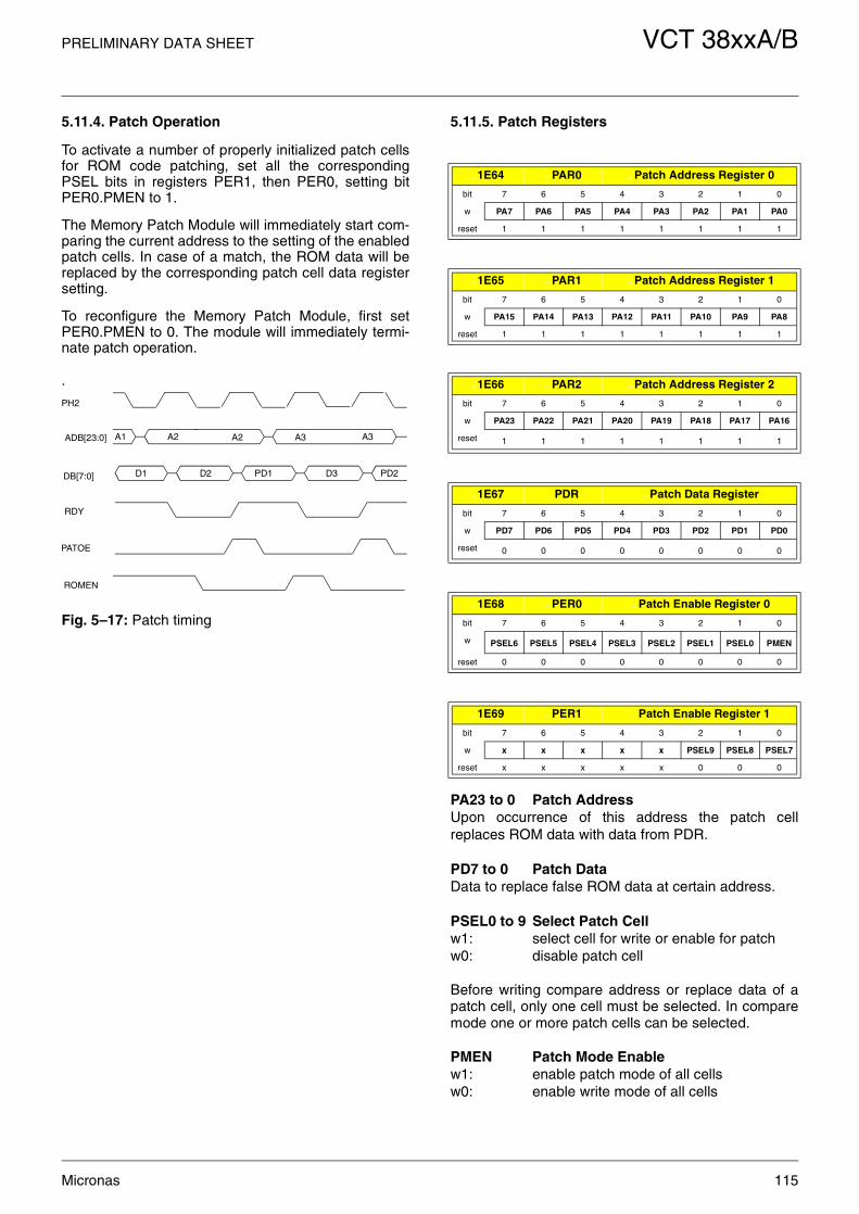
PRELIMINARY DATA SHEET VCT 38xxA/B
Micronas 115
5.11.4. Patch Operation
To activate a number of properly initialized patch cellsfor ROM code patching, set all the correspondingPSEL bits in registers PER1, then PER0, setting bitPER0.PMEN to 1.
The Memory Patch Module will immediately start com-paring the current address to the setting of the enabledpatch cells. In case of a match, the ROM data will bereplaced by the corresponding patch cell data registersetting.
To reconfigure the Memory Patch Module, first setPER0.PMEN to 0. The module will immediately termi-nate patch operation.
.
Fig. 5–17: Patch timing
5.11.5. Patch Registers
PA23 to 0 Patch AddressUpon occurrence of this address the patch cellreplaces ROM data with data from PDR.
PD7 to 0 Patch DataData to replace false ROM data at certain address.
PSEL0 to 9 Select Patch Cellw1: select cell for write or enable for patchw0: disable patch cell
Before writing compare address or replace data of apatch cell, only one cell must be selected. In comparemode one or more patch cells can be selected.
PMEN Patch Mode Enablew1: enable patch mode of all cellsw0: enable write mode of all cells
ADB[23:0]
RDY
PATOE
DB[7:0]
ROMEN
PH2
A2 A2 A3A1 A3
D2D1 PD1 D3 PD2
160: 1E64 161: PAR0 162: Patch Address Register 0
bit 7 6 5 4 3 2 1 0
w PA7 PA6 PA5 PA4 PA3 PA2 PA1 PA0
reset 1 1 1 1 1 1 1 1
163: 1E65 164: PAR1 165: Patch Address Register 1
bit 7 6 5 4 3 2 1 0
w PA15 PA14 PA13 PA12 PA11 PA10 PA9 PA8
reset 1 1 1 1 1 1 1 1
166: 1E66 167: PAR2 168: Patch Address Register 2
bit 7 6 5 4 3 2 1 0
w PA23 PA22 PA21 PA20 PA19 PA18 PA17 PA16
reset 1 1 1 1 1 1 1 1
169: 1E67 170: PDR 171: Patch Data Register
bit 7 6 5 4 3 2 1 0
w PD7 PD6 PD5 PD4 PD3 PD2 PD1 PD0
reset 0 0 0 0 0 0 0 0
172: 1E68 173: PER0 174: Patch Enable Register 0
bit 7 6 5 4 3 2 1 0
w PSEL6 PSEL5 PSEL4 PSEL3 PSEL2 PSEL1 PSEL0 PMEN
reset 0 0 0 0 0 0 0 0
175: 1E69 176: PER1 177: Patch Enable Register 1
bit 7 6 5 4 3 2 1 0
w x x x x x PSEL9 PSEL8 PSEL7
reset x x x x x 0 0 0

VCT 38xxA/B PRELIMINARY DATA SHEET
116 Micronas
5.12. I2C-Bus Master Interface
The I2C bus interface is a pure Master system, Multi-master busses are not realizable. The clock and dataterminal pins have open-drain outputs.
The I2C bus master interface can operate on two ter-minals. Terminal 1 is connected to the pins SDA/SCL,terminal 2 can be connected either to the pinsP36/P37 or to the pins P22/P23. Please refer to chap-ter 5.19. on page 137 how to set up the correspondingport pins.
The I2C bus master interface is not affected by CPUSlow mode.
The bit rate is programmable using a clock prescaler.
A complete telegram is assembled by the software outof individual sections. Each section contains an 8-bitdata. This data is written into one of the six possibleWrite registers. Depending on the chosen address, acertain part of an I2C bus cycle is generated. Bymeans of corresponding calling sequences it is there-fore possible to join even very long telegrams (e.g.long data files for auto increment addressing of I2Cslaves).
The software interface contains a 5 word deep Write-FIFO for the control data registers, as well, as a 3 worddeep Read FIFO for the received data. Thus most ofthe I2C telegrams can be transmitted to the hardwarewithout the software having to wait for empty space inthe FIFO.
An interrupt is generated on two conditions:
– The Write-FIFO was filled and reaches the ‘half full’ state.
– The Write-FIFO is empty and stop condition is com-pleted.
All address and data fields appearing on the bus areconstantly monitored and written into the Read-FIFO.The software can then check these data in comparisonwith the scheduled data. If a read instruction is han-dled, the interface must set the data word FFH, so thatthe responding slave can insert its data. In this casethe Read-FIFO contains the read-in data.
If telegrams longer than 3 bytes (1 address, 2 databytes) are received, the software must check the fillingcondition of the Write-FIFO and, if necessary, fill it up(or read out the Read-FIFO). A variety of status flags isavailable for this purpose:
– The ‘half full’ flag I2CRS.WFH is set if the Write-FIFO is filled with three bytes.
– The ‘empty’ flag I2CRS.RFE is set if there is no more data available in the Read-FIFO.
– The ‘busy’ flag I2CRS.BUSY is activated by writing any byte to any one of the Write registers. It stays active until the I2C bus activities are stopped after the stop condition generation.
Moreover, the ACK-bit is recorded separately on thebus lines for the address and the data fields. However,the interface itself can set the address ACK=0. In anycase the two ACK flags show the actual bus condition.These flags remain until the next I2C start condition isgenerated.
For example, the software has to work off the followingsequence (ACK=1) to read a 16-bit word from an I2Cdevice address 10H (on condition that the bus is notactive):
– write 021H to I2CWS0
– write 0FFH to I2CWD0
– write 0FFH to I2CWP0
– read RFE bit from I2CRS
– read dev. address from I2CRD
– read RFE bit from I2CRS
– read 1st data byte from I2CRD
– read RFE bit from I2CRS
– read 2nddata byte from I2CRD
The value 21H in the first step results from the deviceaddress in the 7 MSBs and the R/W-bit (read=1) in theLSB. If the telegrams are longer, the software has toensure that neither the Write-FIFO nor the Read-FIFOcan overflow.
– To write data to this device:
– write 20H to I2CWS0
– write 1st data byte to I2CWD0
– write 2nd data byte to I2CWP0
The bus activity starts immediately after the first writeto the Write-FIFO. The transmission can be synchro-nized by an artificial extension of the Low phase of theclock line. Transmission is not continued until the stateof the clock line is High once again. Thus, an I2C slavedevice can adjust the transmission rate to its own abili-ties.

PRELIMINARY DATA SHEET VCT 38xxA/B
Micronas 117
Fig. 5–18: Block diagram of I2C bus master interface
AddressDecoder
WR_Data (subaddress=control info)
SRin out
WriteFIFO5 x 11
WR
D0 to D7
control
ReadFIFO3 x 8
D0 to D7
Read Logic
half full
S R
Q
S R
Q
busy
Write Logic
empty Start Conditionresets ACK flags
2
2
Terminal 1SDA/SCL
Terminal 2P22/P23P36/P37
D0 to D7 RD_Status
DA
T_A
CK
AD
R_A
CK
I2CInterrupt
RD_Data
empty
Status Register
clk = fOSCClock Prescaler
SR2.I2C
0
1

VCT 38xxA/B PRELIMINARY DATA SHEET
118 Micronas
Fig. 5–19: Start condition I2C bus
Fig. 5–20: Single bit on I2C bus
Fig. 5–21: Stop condition I2C bus
5.12.1. I2C Bus Master Interface Registers
Writing this register moves I2C start condition, I2CAddress and ACK=1 into the Write FIFO.
Writing this register moves I2C start condition, I2CAddress and ACK=0 into the Write FIFO.
Writing this register moves I2C Data and ACK=1 intothe Write FIFO.
Writing this register moves I2C Data and ACK=0 intothe Write FIFO.
Writing this register moves I2C Data, ACK=1 and I2Cstop condition into the Write FIFO.
Writing this register moves I2C Data, ACK=0 and I2Cstop condition into the Write FIFO.
1T
1T1/2T
SDA
SCL
1/4T
repeated8 times
SDA
SCL
1/2T1/4T 1/4T
1T
SDA
SCL
3/4T1/4T
178: 1FD0 179: I2CWS0 180: I2C Write Start Register 0
bit 7 6 5 4 3 2 1 0
w I2C Address
reset 0 0 0 0 0 0 0 0
181: 1FD1 182: I2CWS1 183: I2C Write Start Register 1
bit 7 6 5 4 3 2 1 0
w I2C Address
reset 0 0 0 0 0 0 0 0
184: 1FD2 185: I2CWD0 186: I2C Write Data Register 0
bit 7 6 5 4 3 2 1 0
w I2C Data
reset 0 0 0 0 0 0 0 0
187: 1FD3 188: I2CWD1 189: I2C Write Data Register 1
bit 7 6 5 4 3 2 1 0
w I2C Data
reset 0 0 0 0 0 0 0 0
190: 1FD4 191: I2CWP0 192: I2C Write Stop Register 0
bit 7 6 5 4 3 2 1 0
w I2C Data
reset 0 0 0 0 0 0 0 0
193: 1FD5 194: I2CWP1 195: I2C Write Stop Register 1
bit 7 6 5 4 3 2 1 0
w I2C Data
reset 0 0 0 0 0 0 0 0

PRELIMINARY DATA SHEET VCT 38xxA/B
Micronas 119
Reading this register returns the content of the ReadFIFO.
OACK “OR”ed Acknowledger: AACK || DACK
AACK Address Acknowledger: Acknowledge state of address field
DACK Data Acknowledger: Acknowledge state of data field
BUSY Busyr1: I2C Master Interface is busyr0: I2C Master Interface is not busy
WFH Write-FIFO Half Fullr1: Write-FIFO is filled with 3 Bytesr0: Write-FIFO is not half full
RFE Read-FIFO Emptyr1: Read-FIFO is emptyr0: Read-FIFO is not empty
TERM Terminal Selectw1: Terminal 1w0: Terminal 2
SPEED Speed Selectw: I2C Bit Rate = fOSC / (4 * SPEED)
SIPS Special Input Port Selectw1: use port pair P36, P37 for terminal 2w0: use port pair P22, P23 for terminal 2
196: 1FD6 197: I2CRD 198: I2C Read Data Register
bit 7 6 5 4 3 2 1 0
r I2C Data
reset 0 0 0 0 0 0 0 0
199: 1FD7 200: I2CRS 201: I2C Read Status Register
bit 7 6 5 4 3 2 1 0
r x OACK AACK DACK BUSY WFH RFE x
reset 0 0 0 0 0 0 0 0
202: 1FDB 203: I2CM 204: I2C Mode Register
bit 7 6 5 4 3 2 1 0
w TERM SPEED
reset 1 0 0 0 0 0 1 0
Table 5–8: I2C Bit Rates
SPEED Bit Rate
0 19.776 Kbit/s
1 2.531 Mbit/s
2 1.266 Mbit/s
3 844 Kbit/s
4 633 Kbit/s
... ...
127 19.931 Kbit/s
205: 1E73 206: I2CPS 207: I2C Port Select Register
bit 7 6 5 4 3 2 1 0
w SIPS
reset 0 0 0 0 0 0 0 0

VCT 38xxA/B PRELIMINARY DATA SHEET
120 Micronas
5.13. Timer T0 and T1
Timer T0 and T1 are 16-bit auto reload down counters.They serve to deliver a timing reference signal, to out-put a frequency signal or to produce time stamps.
5.13.1. Features
– 16-bit auto reload counter
– Time value readable
– Interrupt source output
– Frequency output
5.13.2. Operation
The timer’s 16-bit down-counter is clocked by the inputclock and counts down to zero. Reaching zero, it gen-erates an output pulse, reloads with the content of theTIMx reload register and restarts its travel.
T0 and T1 are not affected by CPU Slow mode.
The clock input frequency can be selected from threepossible values by programming the timer mode regis-ter TIMxM.CSF. After reset, both timers are in standbymode (inactive).
Prior to entering active mode, proper SW initializationof the Ports assigned to function as Tx-OUT outputshas to be made. The ports have to be configured Spe-cial Out (see Section 5.19. on page 137).
To initialize a timer, Reload register TIMx has to set tothe desired time value, still in standby mode. For enter-ing active mode, set the corresponding enable bit inthe Standby register. The timer will immediately startcounting down from the time value present in registerTIMx.
During active mode, a new time value is loaded bywriting to the 16-bit register TIMx, High byte first. Uponwriting the Low byte, the reload register is set to thenew 16-bit value, the counter is reset, and immediatelystarts down-counting with the new value.
On reaching zero, the counter generates a reload sig-nal, which can be used to trigger an interrupt. Thesame signal is connected to a divide by two scaler togenerate the output signal Tx-OUT with a pulse dutyfactor of 50 %.
The interrupt source output of this module is routed tothe Interrupt Controller logic (see Section 5.10. onpage 104).
The state of the down-counter is readable by readingthe 16-bit register TIMx, Low byte first. Upon readingthe Low byte, the High byte is saved to a temporarylatch, which is then accessed during the subsequentHigh byte read.
Thus, for time stamp applications, read consistencybetween Low and High byte is guaranteed.
Returning a timer to standby mode by resetting thecorresponding Enable bit will halt its counter and willset its output to Low. The register TIMx remainsunchanged.
Fig. 5–22: Block diagram of timer T0 and T1
1/2
16
zero16 bit Auto-reloadDown counter
Reload-reg.
TIM x
w
r
TIM xTxInterruptSource
clk
Tx-OUT
3:1MUX
fOSC/21
fOSC/29
fOSC/217
2TIMxM.CSF SR1.TIMx
0
1

PRELIMINARY DATA SHEET VCT 38xxA/B
Micronas 121
5.13.3. Timer Registers
TIMx have to be read Low byte first and written Highbyte first.
CSF Clock Selection Fieldr/w: Source of timer clock (see Table 5–9)
208: 1F4E 209: TIM0L 210: Timer 0 Low Byte
211: 1F4C 212: TIM1L 213: Timer 1 Low Byte
bit 7 6 5 4 3 2 1 0
r Read Low Byte of down-counter and latch High Byte.
w Write Low Byte of reload value and reload down-counter.
reset 1 1 1 1 1 1 1 1
214: 1F4F 215: TIM0H 216: Timer 0 High Byte
217: 1F4D 218: TIM1H 219: Timer 1 High Byte
bit 7 6 5 4 3 2 1 0
r Read latched High Byte of down-counter.
w Write High Byte of reload value.
reset 1 1 1 1 1 1 1 1
220: 1F11 221: TIM0M 222: Timer 0 Mode
223: 1F13 224: TIM1M 225: Timer 1 Mode
bit 7 6 5 4 3 2 1 0
r/w CSF
reset 0 0 0 0 0 0 0 0
Table 5–9: CSF usage
CSF Clock Divider
Timer Clock
Timer Increment
Timer Period
00 fOSC/21 5.0625 MHz 197.53 ns 12.945 ms
01 fOSC/29 19.775 KHz 50.568 µs 3.3140 s
1x fOSC/217 77.248 Hz 12.945 ms 848.39 s

VCT 38xxA/B PRELIMINARY DATA SHEET
122 Micronas
5.14. Capture Compare Module (CAPCOM)
The Capture Compare Module (CAPCOM) is a com-plex relative timer. It comprises a free running 16-bitCapture Compare Counter (CCC) and 2 Capture Com-pare Subunits (SU). The CCC provides an interrupt onoverflow and the timer value can be read by software.
A SU is able to capture the relative time of an externalevent input and to generate an output signal when theCCC passes a predefined timer value. Three types ofinterrupts enable interaction with SW. Special function-ality provides an interface to the asynchronous exter-nal world.
5.14.1. Features
– 16-bit free running counter with read out.
– 16-bit capture register.
– 16-bit compare register.
– Input trigger on rising, falling or both edges.
– Output action: toggle, Low or High level.
– Three different interrupt sources: overflow, input, compare
– Designed for interfacing to asynchronous external events
Fig. 5–23: Block diagram of CAPCOM module
A
B=
&
>1
00
11
01
01
00
11
01
01
TOGGLELow
7 6 5 4 3 2 1 0 7 6 5 4 3 2 1 0
2
MSK MSK MSK FOLCAP CMP OFL LAC RCR X X X
16-Bit Compare-Register
16-Bit Capture-Register r
w
16
16
3 2
01
2
ofl
CC0MCC0I
CC0
>1
load
CC0COMP
CC0OR
IAMOAM
&
&
reset
Output Action Logic
Input Action Logic InterruptSource
InterruptSource
16
Subunit 0
CCCclk
CC0-IN
CC0-OUT
16Timer Value
Subunit 1CC1-IN
CC1-OUT
SR0.CCC
oflTimer Value
CCCOFLInterruptSource
CC1ORInterruptSource
CC1COMPInterruptSource
2CCCS.CSF
4:1Mux
fOSC/20
fOSC/24
fOSC/28
fOSC/212
0
1

PRELIMINARY DATA SHEET VCT 38xxA/B
Micronas 123
5.14.2. Initialization
After system reset the CCC and all SUs are in standbymode (inactive).
In standby mode, the CCC is reset to value 0000h.Capture and compare registers CCx are reset. Noinformation processing will take place, e.g. update ofinterrupt flags. However, the values of registers CCxIand CCxM are only reset by system reset, not bystandby mode. Thus, it is possible to program all modebits in standby mode and a predetermined start-up outof standby mode is guaranteed.
Prior to entering active mode, proper SW configurationof the Ports assigned to function as Input Captureinputs and Output Action outputs has to be made. TheOutput Action ports have to be configured as SpecialOut and the Input Capture ports as special in (seeSection 5.19. on page 137).
Please note, that the compare register CCx is reset instandby mode. It can only be programmed in activemode.
5.14.3. Operation of CCC
For entering active mode of the entire CAPCOM mod-ule set, the enable bit in the standby register.
The CCC will immediately start up-counting with theselected clock frequency and will deliver this 16-bitvalue to the SUs.
The state of the counter is readable by reading the 16-bit register CCC, Low byte first. Upon reading the Lowbyte, the High byte is saved to a temporary latch,which is then accessed during the subsequent Highbyte read. Thus, for time stamp applications, read con-sistency between Low and High byte is guaranteed.
The CCC is free running and will overflow from time totime. This will cause generation of an overflow inter-rupt event. The interrupt (CCCOFL) is directly fed tothe Interrupt Controller and also to all SUs where fur-ther processing takes place.
5.14.3.1. Operation of Subunit
For a proper setup the SW has to program the follow-ing SU control bits in registers CCxI and CCxM: Inter-rupt Mask (MSK), Force Output Logic (FOL, 0 recom-mended), Output Action mode (OAM), Input Actionmode (IAM), Reset Capture register (RCR, 0 recom-mended), and Lock After Capture (LAC). Refer to sec-tion 5.14.5. for details.
Each SU is able to capture the CCC value at a point oftime given by an external input event processed by anInput Action Logic.
A SU can also change an output line level via an Out-put Action Logic at a point of time given by the CCCvalue.
Thus, a SU contains a 16-bit capture register CCx tostore the input event CCC value, a 16-bit compare reg-ister CCx to program the Output Action CCC value, an8-bit interrupt register CCxI and an 8-bit mode registerCCxM. Two types of interrupts per SU enable interac-tion with SW.
For limitations on operating the CAPCOM module inCPU Slow mode, see section 5.14.3.4. on page 124.
5.14.3.2. Compare and Output Action
To activate a SUs compare logic the respective 16-bitcompare register CCx has to be programmed, Lowbyte first. The compare action will be locked until theHigh byte write is completed. As soon as CCx settingand CCC value match, the following actions are trig-gered:
– The flag CMP in the CCxI register is set.
– The CCxCOMP interrupt source is triggered.
– The CCxOR interrupt source is triggered when acti-vated.
– The Output Action logic is triggered. Four different reactions are selectable for the Output Action signal: according to field CCxM.OAM (Table ) the equal state will lead to a High or Low level, or toggling or inactivity on this output. Another means to control the Output Action is bit CCxM.FOL. E.g. rise-mode and force will set the output pin to High level, fall-mode and force to Low level. This forcing is static, i.e. it will be permanently active and may override compare events. Thus, it is recommended to set and reset shortly after that, i.e. to pulse the bit with SW. Toggle mode of the Output Action logic and forcing leads to a burst with clock-frequency and is not recommended.

VCT 38xxA/B PRELIMINARY DATA SHEET
124 Micronas
5.14.3.3. Capture and Input Action
The Input Action logic operates independently of theOutput Action logic and is triggered by an externalinput in a way defined by field CCxM.IAM. FollowingTable 5–12 it can completely ignore events, trigger onrising or falling edge or on both edges. When trig-gered, the following actions take place:
– Flag CCxI.CAP is set.
– The CCxOR interrupt source is triggered when acti-vated.
– The 16-bit capture register CCx stores the current CCC value, i.e. the “time” of the external event. Read CCx Low byte first. Further compare action will be locked until the subsequent High byte read is completed. Thus a coherent result is ensured, no matter how much time has elapsed between the two reads.
Some applications suffer from fast input bursts and alot of capture events and interrupts in consequence. Ifthe SW cannot handle such a rate of interrupts, thiscould evoke stack overflow and system crash. To pre-vent such fatal situations the Lock After Capture (LAC)mode is implemented. If bit CCxI.LAC is set, only onecapture event will pass. After this event has triggered acapture, the Input Action logic will lock until it isunlocked again by writing an arbitrary value to registerCCxM. Make sure that this write only restores thedesired setting of this register.
Programming the Input Action logic while an input tran-sition occurs may result in an unexpected triggering.This may overwrite the capture register, lock the InputAction logic if in LAC mode and generate an interrupt.Make sure that SW is prepared to handle such a situa-tion.
For testing purposes, a permanent reset (FFFFh) maybe forced on capture register CCx by setting bitCCxI.RCR. Make sure that the reset is only temporary.
5.14.3.4. Interrupts
Each SU supplies two internal interrupt events:
1. Input Capture event and
2. Comparator equal state.
As previously explained, interrupt events will set thecorresponding flags in register CCxI. In addition to theabove mentioned two, the CCC Overflow interruptevent sets flag CCxI.OFL in each SU. Thus, threeinterrupt events are available in each SU. The corre-sponding flags are masked with their mask bits in reg-ister CCxM and passed to a logical or. The result(CCxOR) is fed to the Interrupt Controller as a firstinterrupt source. In addition, the Comparator equal(CCxCOMP) interrupt is directly passed to the InterruptController as second interrupt source. Thus a SUoffers four types of interrupts: CCC overflow(maskable ored), input capture event (maskable ored)
and comparator equal state (maskable ored and non-maskable direct).
All interrupt sources act independently, parallel inter-rupts are possible. The interrupt flags enable SW todetermine the interrupt source and to take the appro-priate action. Before returning from the interrupt rou-tine the corresponding interrupt flag should thus becleared by writing a 1 to the corresponding bit locationin register CCxI.
The interrupts generated by internal logic (CCC Over-flow and Comparator equal) will trigger in a predeter-mined and known way. But as explained in 5.14.3.3.erroneous input signals may cause some difficultiesconcerning the Input Capture input, as well, as inter-rupt handling. To overcome possible problems theInput Capture Interrupt flag CCxI.CAP is double buff-ered. If a second or even more input capture interruptevents occur before the interrupt flag is cleared (i.e.SW was not able to keep track), the flag goes to a thirdstate. Two consecutive writes to this bit in registerCCxI are then necessary to clear the flag. This enablesSW to detect such a multiple interrupt situation andeventually to discard the capture register value whichalways relates to the latest input capture event andinterrupt.
The internal CAPCOM module control logic alwaysruns on the oscillator frequency, regardless of CPUSlow mode. Avoid write accesses to the CCxI registerin CPU Slow mode, since the logic would interpret oneCPU access as many consecutive accesses. This mayyield unexpected results concerning the functionality ofthe interrupt flags. The following procedure should befollowed to handle the capture interrupt flag CAP:
1. SW responds to a CAPCOM interrupt, switching to CPU Fast mode if necessary and determining that the source is a capture interrupt (CAP flag =1).
2. The interrupt service routine is processed.
3. Just before returning to main program, the service routine acknowledges the interrupt by writing a 1 to flag CAP.
4. The service routine reads CAP again. If it is reset, the routine can return to main program as usual. If it is still set an external capture event overrun has happened. Appropriate actions may be taken (i.e. discarding the capture register value etc.).
5. go to 3.
5.14.4. Inactivation
The CAPCOM module is inactivated and returned tostandby mode (power down mode) by setting theEnable bit to 0. Section 5.14.2. applies. CCxI andCCxM are only reset by system reset, not by standbymode.

PRELIMINARY DATA SHEET VCT 38xxA/B
Micronas 125
5.14.5. CAPCOM Registers
The CAPCOM module counter has to be read Lowbyte first to avoid inconsistencies.
CSF Clock Selection Fieldw: Source of CCC clock (see Table 5–10)Table 5–10: CSF usage
MSK Mask Flagw1: Enable.w0: Disable.
These mask flags refer to the corresponding eventflags in CAPCOM interrupt register.
FOL Force Output Action Logicr/w1: Force Output Action logic.r/w0: Release Output Action logic.
This flag is static. As long as FOL is true neither com-parator can trigger nor SW can force, by writinganother “one”, the Output Action logic. After forcing it isrecommended to clear FOL unless Output Action logicshould not be locked.
OAM Output Action Moder/w: Defines behavior of Output Action logic.
IAM Input Action Moder/w: Defines behavior of Input Action logic.
226: 1F7C 227: CCCL 228: CAPCOM Counter Low Byte
bit 7 6 5 4 3 2 1 0
r Read Low Byte and lock CCC.
reset 0 0 0 0 0 0 0 0
229: 1F7D 230: CCCH 231: CAPCOM Counter High Byte
bit 7 6 5 4 3 2 1 0
r Read High Byte and unlock CCC.
reset 0 0 0 0 0 0 0 0
232: 1F14 233: CCCS 234: CAPCOM Clock Select
bit 7 6 5 4 3 2 1 0
w CSF
reset 0 0 0 0 0 0 0 0
CSF Clock Divider
Timer Clock
Timer Increment
Timer Period
00 fOSC/20 10.125 MHz 98.765 ns 6.4727 ms
01 fOSC/24 632.81 KHz 1.5802 µs 103.56 ms
10 fOSC/28 39.551 KHz 25.284 µs 1.6570 s
11 fOSC/212 2.4719 KHz 404.54 µs 26.512 s
235: 1F6C 236: CC0M 237: CAPCOM 0 Mode Register
238: 1F70 239: CC1M 240: CAPCOM 1 Mode Register
bit 7 6 5 4 3 2 1 0
r MSK MSK MSK FOL OAM IAM
reset 0 0 0 0 0 0 0 0
Table 5–11: OAM usage
OAM Output Action Logic Modes
0 0 Disabled, ignore trigger, output Low level.
0 1 Toggle output.
1 0 Output Low level.
1 1 Output High level.
Table 5–12: IAM usage
IAM Input Action Logic Modes
0 0 Disabled, don’t trigger.
0 1 Trigger on rising edge.
1 0 Trigger on falling edge.
1 1 Trigger on rising and falling edge.
VCT 38xxA/B PRELIMINARY DATA SHEET
126 Micronas
CAP Capture Eventr1: Event. r0: No Event. w1: Clear flag.
CMP Compare Eventr1: Event. r0: No Event.w1: Clear flag.
OVL Overflow Eventr1: Event. r0: No Event. w1: Clear flag.
LAC Lock After Capture r/w1: Enable.r/w0: Disable.
RCR Reset Capture Registerr/w1: Reset capture register to FFFFh. r/w0: Release capture register.
CCSIPn CAPCOM Special Input Port n
This field defines the special input port connected tothe associated SU (see Table on page 137).
241: 1F6D 242: CC0I 243: CAPCOM 0 Interrupt Register
244: 1F71 245: CC1I 246: CAPCOM 1 Interrupt Register
bit 7 6 5 4 3 2 1 0
r/w CAP CMP OFL LAC RCR x x x
reset 0 0 0 0 0 0 0 0
247: 1F6E 248: CC0L 249: CAPCOM 0 Capture/Compare Low Byte
250: 1F72 251: CC1L 252: CAPCOM 1 Capture/Compare Low Byte
bit 7 6 5 4 3 2 1 0
r Read Low Byte of capture register and lock it.
w Write Low Byte of compare register and lock it.
reset 1 1 1 1 1 1 1 1
253: 1F6F 254: CC0H 255: CAPCOM 0 Capture/Compare High Byte
256: 1F73 257: CC1H 258: CAPCOM 1 Capture/Compare High Byte
bit 7 6 5 4 3 2 1 0
r Read High Byte of capture register and unlock it.
w Write High Byte of compare register and unlock it.
reset 1 1 1 1 1 1 1 1
259: 1E70 260: CCIMUX 261: CAPCOM Input Multiplex Register
bit 7 6 5 4 3 2 1 0
w CCSIP1 CCSIP0
reset 0 0 0 0 0 0 0 0

PRELIMINARY DATA SHEET VCT 38xxA/B
Micronas 127
5.15. Pulse Width Modulator
Each of the 4 available PWMs is an 8-bit reload down-counter with fixed reload interval. It serves to generatea frequency signal with variable pulse width or, with anexternal low-pass filter, as a digital to analog con-verter.
5.15.1. Features
– 8-bit resolution
– standby mode
5.15.2. General
A PWM’s 8-bit down-counter is clocked by its inputclock and counts down to zero. Reaching zero, it stopsand sets the output to Low. A load pulse reloads thecounter with the content of the PWM register, restartsit and sets the output to High. The repetition rate is19.775 KHz, the reload period is 50.57 µs.
The PWMs are not affected by CPU Slow mode. It isrecommended that the CPU should not write the PWMregisters during Slow mode.
5.15.3. Initialization
Prior to entering active mode, proper SW initializationof the Ports assigned to function as PWMx outputs hasto be made. The ports have to be configured SpecialOut (see Section 5.19. on page 137).
5.15.4. Operation
After reset, all PWMs are in standby mode (inactive)and the output signal PWMx is Low.
For entering active mode, the enable bit in the corre-sponding standby register has to be set (see Section5.5. on page 93). The desired pulse width value isthen written into register PWMx. Each PWM will start
producing its output signal immediately after the nextsubsequent load pulse.
During active mode, a new pulse width value is set bysimply writing to the register PWMx. Upon the nextsubsequent load pulse the PWM will start producingan output signal with the new pulse width value, start-ing with a High level.
Returning a PWM to standby mode by resetting itsrespective enable flag will immediately set its outputLow.
The state of the down-counters is not readable.
5.15.5. PWM Registers
Fig. 5–24: Block diagram of 8-bit PWM
262: 1F50 263: PWM0 264: PWM 0 Register
265: 1F51 266: PWM1 267: PWM 1 Register
268: 1F52 269: PWM2 270: PWM 2 Register
271: 1F53 272: PWM3 273: PWM 3 Register
bit 7 6 5 4 3 2 1 0
w Pulse width value
reset 0 0 0 0 0 0 0 0
Table 5–13: Pulse Width Programming
Pulse width value Pulse duty factor
00h 0% (Output is static Low)
01h 1/256
02h 2/256
: :
FEh 254/256
FFh 100% (Output is static High) 1)
1) Pulse duty factor 255/256 is not selectable.
x: PWM number 0 to 3y: Standby Register 0 or 2
8
zero
Pulse Width Register
PWMx
w
clk
S Q
R
1
0
load
8-bit down counter
1
0
SRy.PWMx
PWMx
1
0
fOSC/21
fOSC/29

VCT 38xxA/B PRELIMINARY DATA SHEET
128 Micronas
5.16. Tuning Voltage Pulse Width Modulator
The Tuning Voltage Pulse Width Modulator (TVPWM),in combination with an external low pass filter, servesas a digital to analog converter to control voltage syn-thesis tuning. It can also be operated as a normal 8-bitPWM.
5.16.1. Features
– 14bit resolution
– standby mode
5.16.2. General
The TVPWM is based on an 8-bit PWM built by acounter and a programmable comparator (see Fig. 5–26). The overflow of the counter reloads the compara-tor with the content of the TVPWMH register and setsthe TVPWM output to High. Matching the countervalue, the comparator sets the TVPWM output to Low.The counter is continually running, producing PWMcycles with a length of 256 T.
Depending on the content of the TVPWML register,the 6-bit pulse extension logic will add additional singleclock pulses distributed over a frame of 64 reloadcycles (see Fig. 5–25). This gives 14-bit resolutionwhen integrating over a complete frame. The framerate is 309 Hz, the frame period is 3.24 ms.
An interrupt is generated after completion of a frame of64 reload cycles. The interrupt source output of thismodule is routed to the Interrupt Controller logic (seeSection 5.10. on page 104).
The TVPWM is not affected by CPU Slow mode. It isrecommended that the CPU should not write theTVPWM registers during Slow mode.
Fig. 5–25: TVPWM Timing
Fig. 5–26: Block Diagram of 14bit Tuning Voltage PWM
cycle n cycle n+1
256 T 256 T
1 T
TVPWML Register
8
TVPWMH Registerw
clk1
0
8 bit PWM Counter
SR0.TVPWM
TVPWM
fOSC/21
6
≥1
TVPWMInterruptSource
6 bit Frame Counterload
Comparator Extension Logic
pwm
pulse
8 6
PRELIMINARY DATA SHEET VCT 38xxA/B
Micronas 129
5.16.3. Initialization
Prior to entering active mode, proper SW initializationof the Ports assigned to function as TVPWM outputhas to be made. The ports have to be configured Spe-cial Out (see Section 5.19. on page 137).
5.16.4. Operation
After reset, the TVPWM is in standby mode (inactive)and the output signal TVPWM is Low.
For entering active mode, the enable bit in the corre-sponding standby register has to be set (see Section5.5. on page 93). The desired pulse width value isthen written into the registers TVPWML and TVP-WMH. The TVPWM will start producing its output sig-nal immediately after the next subsequent load pulse.
During active mode, a new pulse width value is set bysimply writing to the register TVPWML and TVPWMH.Writing TVPWMH will update the comparator and theextension logic with the new register values. Upon thenext subsequent load pulse the TVPWM will start pro-ducing an output signal with the new pulse width value,starting with a High level.
Returning the TVPWM to standby mode by resettingits respective enable flag will not reset its output signal.
The state of the counters and the extension logic is notreadable.
5.16.5. TVPWM Registers
TVPWM has to be written Low byte first.
274: 1F4A 275: TVPWML 276: TV PWM Low Byte
bit 7 6 5 4 3 2 1 0
w Pulse width value Low
reset 0 0 0 0 0 0
277: 1F4B 278: TVPWMH 279: TV PWM High Byte
bit 7 6 5 4 3 2 1 0
w Pulse width value High
reset 0 0 0 0 0 0 0 0

VCT 38xxA/B PRELIMINARY DATA SHEET
130 Micronas
5.17. A/D Converter (ADC)
This 10-bit analog to digital converter allows the con-version of an analog voltage in the range of 0 toVSUPS into a digital value. A multiplexer connects theADC to one of 15 analog input ports. A sample-and-hold circuit holds the analog voltage during conver-sion. The duration of the sampling time is programma-ble. The A/D conversion is done by a charge balanceA/D converter using successive approximation.
5.17.1. Features
– A/D converter with 10-bit resolution.
– Successive approximation, charge balance type.
– Input multiplexer with 15 analog channels.
– Sample and hold circuit.
– 4/8/16/32 µs conversion selectable for optimum throughput/accuracy balance.
– Zero standby current, 300 µA active current.
Fig. 5–27: Block Diagram of the ADC
P10-17A
DS&H
x x x x
TSAMP CHANNELAD0AD1
01234567 01234567
9 8 7 4 3 2 1 0
VSUPS
0
1
GNDS 4
SR1.ADC
EOCCMPO CMPO
2
10
r
w
r
56
InterruptSource
MUX15
P20-26

PRELIMINARY DATA SHEET VCT 38xxA/B
Micronas 131
5.17.2. Operation
After reset, the module is off (zero standby current).The module is enabled by the flag SR1.ADC. The usermust ensure that the flag End of Conversion (EOC) inregister AD0 is true, before he starts to operate themodule.
A write access to register AD0 indicating sample timeand channel number starts the conversion. The flagEOC signalizes the end of conversion. The 10-bitresult is stored in the registers AD1 (8 MSB) and AD0.The conversion rate depends on the software, theoscillator frequency and the programmed sample time.
The ADC module is not affected by CPU Slow mode.
5.17.3. Measurement Errors
The result of the conversion mirrors the voltage poten-tial of the sampling capacitance (typically 15 pF) at theend of the sampling time. This capacitance has to becharged by the source through the source impedancewithin the sampling time period. To avoid measure-ment errors, system design has to make sure that atthe end of the sampling period, the potential error onthe sampling capacitance is less than ±0.1 LSB.
Measurement errors may occur, when the voltage ofhigh-impedance sources has to be measured:
– To reduce these errors, the sampling time may be increased by programming the field TSAMP in reg-ister AD1.
– In cases where high-impedance sources are only rarely sampled, a 100-nF capacitor from the input to GNDS is a sufficient measure to ensure that the potential on the sampling capacitance reaches the full source potential, even with the shortest sam-pling time.
– In some high-impedance applications a charge pumping effect may influence the measurement result when two sources are measured alternatingly.
5.17.4. Comparator
In addition to the A/D converter the module contains acomparator. The level at the A/D converter input iscompared to VSUPS/2. The state of the comparatoroutput can be read at flag CMPO in register AD0.
The interrupt source output of this module is routed tothe Interrupt Controller logic. The CMPO interruptsource is gated with an internal clock. This is the rea-son why interrupts are generated as long as the levelat the comparator is lower than the internal reference.

VCT 38xxA/B PRELIMINARY DATA SHEET
132 Micronas
5.17.5. ADC Registers
A write access to register AD0 starts the A/D conver-sion of the written channel number and sampling dura-tion. The flag EOC signals the end of conversion. Theresult is stored in register AD1 (bit 9 to 2) and in regis-ter AD0 (bit 1 and 0).
EOC End of Conversionr1: End of conversionr0: Busy
EOC is reset by a write access to the register AD0.EOC must be true before starting the first conversionafter enabling the module by setting SR1.ADC.
CMPO Comparator Outputr1: Input is lower than reference voltage. r0: Input is higher than reference voltage.
TSAMP Sampling Time
TSAMP adjusts the sample time and the conversiontime. The total conversion time is 20 clock cycleslonger than the sample time. Sampling starts one clockcycle after completion of the write access to AD0.
CHANNEL Channel of Input Multiplexer
CHANNEL selects from which port pin the conversionis done. The MSB of CHANNEL is bit 3. No port pin isconnected to the ADC if the channel 0 is selected. Inthis case the input of the A/D converter is connected toground. After reset, CHANNEL is set to zero.
AN 9 to 0 Analog Value Bit 9 to 0
The 10 bit analog value is in the range of 0 to 1023.The 8 MSB can be read from register AD1. The twoLSB can be read from register AD0. The result is avail-able until a new conversion is started.
280: 1FA8 281: AD0 282: ADC Register 0
bit 7 6 5 4 3 2 1 0
r EOC CMPO x x x x AN1 AN0
w TSAMP CHANNEL
reset 0 0 0 0 0 0 0 0
283: 1FA9 284: AD1 285: ADC Register 1
bit 7 6 5 4 3 2 1 0
r AN9 AN8 AN7 AN6 AN5 AN4 AN3 AN2
reset
Table 5–14: Sampling time adjustment
TSAMP tSample tConversion
0H 20 TOSC 40 TOSC
1H 60 TOSC 80 TOSC
2H 140 TOSC 160 TOSC
3H 300 TOSC 320 TOSC
Table 5–15: ADC input multiplexer
CHANNEL Port Pin
0 none
1 P10
2 P11
3 P12
4 P13
5 P14
6 P15
7 P16
8 P17
9 P20
10 P21
11 P22
12 P23
13 P24
14 P25
15 P26

PRELIMINARY DATA SHEET VCT 38xxA/B
Micronas 133
5.18. Closed Caption Module (CC)
The text slicer that is implemented in the TPU is mainlydesigned for teletext applications. Other services asclosed captioning or CGMS data slicing are possiblebut only with limited performance.
Therefore the VCT 38xxB includes a standaloneclosed caption & CGMS decoder module. The moduleis connected to the luma ADC of the video front-endand uses the complete sync slicing of the videofront-end. The decoded information is made availableto the CPU via a set of memory mapped registers.
5.18.1. Features
The decoder supports the following features:
• closed captioning (field 1&2) for US subtitling
• extended data services (XDS):time of day, local time zone, program rating, ...
• CGMS data:copyright info, aspect ratio, indication of protection with split-burst / pseudo-sync pulses
• automatic threshold adaption or programmable fix threshold
Fig. 5–28: Block diagram of Closed Caption Module
Timing
LPF
ThresholdAdaption
Bitslicing
TimingRecovery
ShiftRegister
FormatterControl
Register
HSYNCVSYNCINTERLACE
YIN
Interface

VCT 38xxA/B PRELIMINARY DATA SHEET
134 Micronas
5.18.2. Operation
5.18.2.1. Lowpass filter
The incoming video signal is bandlimited to fg=1 MHzto improve the performance with noisy signals.
5.18.2.2. Input timing
A timing unit generates a horizontal and vertical time-base that is synchronized to the video timing.
The nominal delay between horizontal sync and thebegin of the clock run-in (CRI) of the caption line isspecified to 10.5 us. The window in which the CRI isdetected can be shifted with a programmable 6bit hori-zontal offset. The generated vertical timing can beshifted as well with a programmable vertical offset by+/- 7 lines. Additionally for the second field an offset of+/- 1 line can be selected.
Depending on the active mode, the timing unit gener-ates several enable signals to allow caption & CGMSprocessing. The possible modes are:
• closed caption, line 21, 1st field only
• closed caption, line 21, 2nd field only
• closed caption, line 21, both fields
• CGMS, line 20, both fields
Note that all modes can be combined also.
5.18.2.3. Threshold adaption
If caption data is present, the amplitude of the CRI ismeasured during a fix window with a length of 80cycles. This corresponds to 2 complete periods of theCRI frequency. This result is used as adaptive thresh-old for the bitslicing. If no caption data is present, thedefault or the last measured value is used. The lastvalue is stored and can be read by the CPU. Alterna-tively a fix value can be programmed by the CPU.
For CGMS data, the adaptive or fix threshold can beselected independently. In both cases the correspond-ing value for captioning is used, but is rescaled forCGMS by a factor of 1.4 as the nominal amplitude ofcaption data is 50 IRE and that of CGMS data is 70IRE.
To avoid that in the case of a wrong measurement theadaptive threshold lies completely below or above thesignal range, it is ‘pseudo’ limited to a range of approx-imately 50..150% of the default level. This pseudo-limi-tation is done by forcing the MSBs to a certain rangeand thus remapping forbidden ranges into the allowedregion.
5.18.2.4. Bitslicing
The incoming video signal is compared to the currentlyvalid threshold. The result of this hard decision is usedfor the bit timing recovery. Resampled with the bit tim-ing it leads to the final result of the slicing process.
5.18.2.5. Timing recovery
The bit timing is recovered by a digital PLL using a 15bit accumulator. This accu is incremented with a con-stant value thus generating a fix frequency. Thedetected edges in the bitstream are used for an updateof the phase. For captioning the phase error at theedges is measured and corrected proportionallydepending on a programmable gain. During the CRIthe accu has the same frequency but generates twiceas much sample pulses. For captioning the phaseerrors during a line are accumulated to allow the calcu-lation of the ideal startphase at the begin of a line. Thisvalue is used in the next field. For CGMS the phasecorrection only consists of a hard reset at each edge.An adaption of the startphase is not necessary in thiscase.
5.18.2.6. Shift register
With the sample pulses generated by the timing recov-ery, the shift register latches the actual bit. It stores thelast 8 received bits. When a complete byte has beenreceived, it is moved into the corresponding data regis-ter in the output formatter.
5.18.2.7. Controlling
After the reception of each byte, the control unit gener-ates a latch pulse for the output formatter. When allbytes have been received the status information isupdated to indicate that new data is available.
5.18.2.8. Formatter
The formatter latches all received bytes into the corre-sponding output register. In total there are 6 registers:
– caption status + CGMS status (can be used optionally)
– 1st caption byte
– 2nd caption byte
– CGMS status + CGMS bit[4:1]
– CGMS bit[12:5]
– CGMS bit[20:13]
If the data register is not read before the next byte isreceived, an overflow bit is set in the status register.

PRELIMINARY DATA SHEET VCT 38xxA/B
Micronas 135
5.18.3. CCM Registers
ENCC Enable Closed Captionw0: disable caption acquisitionw1: enable caption acquisition in line 21
FSCC Field Select Closed Captionw00: enable field 1 acquisitionw01: enable field 2 acquisitionw1x: enable field 1+2 acquisition
EFTCC Enable Fix Threshold Closed Captionw0: enable adaptive thresholdw1: enable fix threshold
ROF Reset Overflow Flagsw0: no actionw1: reset overflow flags in status register
ENCGMS Enable CGMSw0: disable CGMS acquisitionw1: enable CGMS acquisition in line 20
SCGMS Short CGMS Modew0: receive full 20bit CGMS dataw1: receive only first 4bit CGMS data
EFTCGMS Enable Fix Threshold CGMSw0: enable adaptive thresholdw1: enable fix threshold
PGAIN Phase Gainw00: loww11: high
FLDOFFS 2nd Field Offsetw00: 0 line offset to 1st fieldw01: +1 line offset to 1st fieldw10: -2 line offset to 1st fieldw11: -1 line offset to 1st field
DV Data Validr0: data invalidr1: data valid
FID Field IDr0: currently available data from field 1r1: currently available data from field 2
OO Overflow Occuredr0: no overflow of data bufferr1: overflow of data buffer
286: 1EB0 287: CCM1 288: CC Mode 1
bit 7 6 5 4 3 2 1 0
r/w ROF EFTCC FSCC ENCC
reset 0 0 0 0 0 0 0 0
289: 1EB1 290: CCM2 291: CC Mode 2
bit 7 6 5 4 3 2 1 0
r/w EFTCGMS
SCGMS ENCGMS
reset 0 0 0 0 0 0 0 0
292: 1EB2 293: CCHTIM 294: CC Horizontal Timing
bit 7 6 5 4 3 2 1 0
r/w PGAIN horizontal offset -32..+31 (in steps of 0.4us)
reset 1 0 0 0 0 0 0 0
295: 1EB3 296: CCVTIM 297: CC Vertical Timing
bit 7 6 5 4 3 2 1 0
r/w FLDOFFS vertical offset -32..+31
reset 0 0 0 0 0 0 0 0
298: 1EB4 299: CCTHR 300: CC Threshold
bit 7 6 5 4 3 2 1 0
r adaptive threshold 0..255
w fix threshold 0..255
reset 0 0 0 0 0 0 0 0
301: 1EB6 302: CCSTAT 303: CC Status
bit 7 6 5 4 3 2 1 0
CGMSSTAT CCSTAT
r OO FID DV OO FID DV
reset 0 0 0 0 0 0 0 0

VCT 38xxA/B PRELIMINARY DATA SHEET
136 Micronas
304: 1EB7 305: CCB1 306: CC Byte 1
bit 7 6 5 4 3 2 1 0
r CC Byte 1
reset 0 0 0 0 0 0 0 0
307: 1EB8 308: CCB2 309: CC Byte 2
bit 7 6 5 4 3 2 1 0
r CC Byte 2
reset 0 0 0 0 0 0 0 0
310: 1EB9 311: CGMS1 312: CC CGMS 1
bit 7 6 5 4 3 2 1 0
CGMSSTAT
r CGMS Bit 4-1 OO FID DV
0 0 0 0 0 0 0 0
313: 1EBA 314: CGMS2 315: CC CGMS 2
bit 7 6 5 4 3 2 1 0
r CGMS Bit 12-5
reset 0 0 0 0 0 0 0 0
316: 1EBB 317: CGMS3 318: CC CGMS 3
bit 7 6 5 4 3 2 1 0
r CGMS Bit 20-13
reset 0 0 0 0 0 0 0 0

PRELIMINARY DATA SHEET VCT 38xxA/B
Micronas 137
5.19. Ports
There exist different kinds of ports. The universalports, P1 to P3, serve as digital I/O and have addi-tional special input and output functions. A subset ofthe universal ports (P10-P17, P20-P26) serves asinput for the analog-to-digital converter. The I2C portsSDA, SCL can alternatively be used as digital I/Oports. The analog audio ports AIN1−3, AOUT1−2 canalternatively be used as digital input ports. The20.25 MHz system clock output CLK20 can alterna-tively be used as digital output port.
5.19.1. Port Assignment
Table 5–17 shows the assignment of port pins to Spe-cial Input and Output functions.
Every Special Output function is connected to 2 portpins in parallel and can be activated via the MOD flagin the corresponding port register.
The ADC input multiplexer can be connected to 1 of 15port pins. The output driver of the selected port pin isthen forced to open-drain mode. Additionally it can bedisabled using the EN flag in the corresponding portregister.
Every special input function can be connected to 1 of15 input ports (see Table 5–16). If port number 0 isselected the special input function is connected toground. Changing the input port may produce tempo-rary glitch signals. Therefore, the corresponding spe-cial input function should be disabled before the inputport is changed.
Table 5–16: Special input configuration
SpecialInputNumber
SpecialInputFunction
SpecialInputPort
1 CC0−IN 0−15
2 CC1−IN 0−15
3 PINT0 0−15
4 PINT1 0−15
5 PINT2 0−15
6 PINT3 0−15
Table 5–17: Port pin configuration
Port Name
ADC Input
Special Output
Special Input Port
P10 1 Timer 0 1
P11 2 Timer 1 2
P12 3 CC0−OUT 3
P13 4 CC1−OUT 4
P14 5 TVPWM 5
P15 6 PWM 0 6
P16 7 PWM 1 7
P17 8 PWM 2 8
P20 9 PWM 3 9
P21 10 CLK20 10
P22 11 SDA 2 11
P23 12 SCL 2 12
P24 13 Timer 0
P25 14 Timer 1
P26 15 CC0−OUT
P27 CC1−OUT
P30 TVPWM
P31 PWM 0
P32 PWM 1
P33 PWM 2
P34 PWM 3
P35 CLK20
P36 SDA 2
P37 SCL 2
P40 SDA
P41 SCL
P42 AOUT1
P43 AOUT2 13
P44 AIN1
P45 AIN2 14
P46 AIN3 15

VCT 38xxA/B PRELIMINARY DATA SHEET
138 Micronas
5.19.2. Universal Ports P1 to P3
There are 24 universal port pins. The universal portsP1 to P3 are each 8 bits wide. In the 64-pin PSDIPpackage only 12 universal port pins are available(P10−P17, P20−P23).
5.19.2.1. Features
– digital I/O port
– special input and output function
– analog input function
– Schmitt trigger input buffer
– tristate output
– push-pull or open-drain output
– 10-mA output current
– output supply either 3.3 V or 5.0 V
Fig. 5–29: Universal port circuit
Universal ports can be operated in different modes.After reset, all Universal Ports are in normal mode,tristate condition.
DQ
DQ
DQ
0
1
Px.y
DBy
Special In x.y
Special Out x.y
PxE
PxM
PxD write
PxD read
x: Port number 1 to 3y: Port pin number 0 to 7
ADC In x.y
VDD
VSS
PxVDD
PxVSS
DQ
PxO
Table 5–18: Universal ports operating modes
Modes Function
Port Mode Normal Input The SW uses the ports as digital input.
Special Input The port input is additionally connected to specific hardware modules.
Normal Output The SW uses the ports as latched digital tristate output.
Special Output The port output is directly driven by specific hardware modules.

PRELIMINARY DATA SHEET VCT 38xxA/B
Micronas 139
5.19.2.2. Universal Port Mode
Each port bit can be individually configured to severalport modes. The output driver of each pin has to beenabled by setting the EN flag. Using the OUT flag theoutput stage can be configured to either open drain orpush pull output. The MOD flag selects the source ofthe output value.
The Special Input mode is always active. This allowsmanipulating the input signal to the special hardwarethrough Normal Output operations by software.
As the Special Output mode allows reading the pin lev-els, the output state of the special hardware may beread by the CPU.
5.19.3. Universal Port Registers
Universal Port Data registers PxD contain input/outputdata of the corresponding port. The “x” in PxD meansthe number of the port. Thus PxD stands for P1D toP3D.
D0−7 Universal Port Data Input/Outputr: Read pin level resp. data latch.w: Write data to data latch.
To use a port pin as software output, the appropriatedriver must be activated by setting the EN flag and theMOD flag must be programmed to Normal mode.
OUT0−7 Output Flagw1: Output driver is open drainw0: Output driver is push pull
MOD0−7 Normal/Special Mode Flagw1: Special Output Modew0: Normal Output Mode
The MOD flag defines from which source the pin isdriven if the EN flag is true.
EN0−7 Enable Flagw1: Output driver is enabled w0: Output driver is disabled
Table 5–19: Port mode register settings
Mode MOD EN D Function
Normal Input
x 0 x READ of register PxD returns port pin input levels to data bus.
Normal Output
0 1 Data WRITE to register PxD changes level of port pin output drivers.
READ of register PxD returns the PxD register set-ting to the data bus.
Special Input
x x x Port pin input level is presented to special hardware.
Special Output
1 1 x Special hardware drives port pin.
READ of register PxD returns port pin input levels to data bus.
319: 1F90 320: P1D 321: Port 1 Data Register
322: 1F94 323: P2D 324: Port 2 Data Register
325: 1F98 326: P3D 327: Port 3 Data Register
bit 7 6 5 4 3 2 1 0
r/w D7 D6 D5 D4 D3 D2 D1 D0
reset 0 0 0 0 0 0 0 0
328: 1F91 329: P1O 330: Port 1 Output Register
331: 1F95 332: P2O 333: Port 2 Output Register
334: 1F99 335: P3O 336: Port 3 Output Register
bit 7 6 5 4 3 2 1 0
w OUT7 OUT6 OUT5 OUT4 OUT3 OUT2 OUT1 OUT0
reset 0 0 0 0 0 0 0 0
337: 1F92 338: P1M 339: Port 1 Mode Register
340: 1F96 341: P2M 342: Port 2 Mode Register
343: 1F9A 344: P3M 345: Port 3 Mode Register
bit 7 6 5 4 3 2 1 0
w MOD7 MOD6 MOD5 MOD4 MOD3 MOD2 MOD1 MOD0
reset 0 0 0 0 0 0 0 0
346: 1F93 347: P1E 348: Port 1 Enable Register
349: 1F97 350: P2E 351: Port 2 Enable Register
352: 1F9B 353: P3E 354: Port 3 Enable Register
bit 7 6 5 4 3 2 1 0
w EN7 EN6 EN5 EN4 EN3 EN2 EN1 EN0
reset 0 0 0 0 0 0 0 0

VCT 38xxA/B PRELIMINARY DATA SHEET
140 Micronas
5.19.4. I2C Ports P40 and P41
The I2C ports SDA and SCL can alternatively be usedas digital I/O ports. To activate the I2C function of theport pin the corresponding MOD flag has to be set tospecial mode. In normal mode the port pin serves asdigital I/O. The output stage is open-drain only. Afterreset, the I2C ports are in special mode.
5.19.4.1. Features
– digital I/O port
– I2C input and output function
– Schmitt trigger input buffer
– open-drain output– connected to standby supply
SCLD SCL Data Input/Outputr: Read pin level resp. data latch.w: Write data to data latch.
SDAD SDA Data Input/Outputr: Read pin level resp. data latch.w: Write data to data latch.
To use the I2C ports as software output, the appropri-ate drivers must be activated by setting the SCLENand SDAEN flag and resetting the SCLM and SDAMflags.
SCLM SCL Normal/Special Mode Flagw1: Special I2C Output Modew0: Normal Output Mode
SDAM SDA Normal/Special Mode Flagw1: Special I2C Output Modew0: Normal Output Mode
SCLEN SCL Enable Flagw1: Output driver is enabled w0: Output driver is disabled
SDAEN SDA Enable Flagw1: Output driver is enabled w0: Output driver is disabled
Fig. 5–30: I2C port circuit
355: 1F9C 356: P4D 357: Port 4 Data Register
bit 7 6 5 4 3 2 1 0
r AIN3D AIN2D AIN1D AOUT2D AOUT1D SCLD SDAD
w SCLD SDAD
reset 0 0 0 0 0 0 0
358: 1F9E 359: P4M 360: Port 4 Mode Register
bit 7 6 5 4 3 2 1 0
w AIN3M AIN2M AIN1M AOUT2M AOUT1M SCLM SDAM
reset 1 1 1 0 0 1 1
361: 1F9F 362: P4E 363: Port 4 Enable Register
bit 7 6 5 4 3 2 1 0
w SCLEN SDAEN
reset 1 1
DQ
DQ
DQ
0
1P40
DB0/DB1
SDA/SCL In
SDA/SCL Out
P4E
P4M
P4D write
P4D readVDD
VSS
VDD
VSS
P41
0
1

PRELIMINARY DATA SHEET VCT 38xxA/B
Micronas 141
5.19.5. Audio Ports P42 to P46
The analog audio ports AIN1−3, AOUT1−2 can alter-natively be used as digital input ports. To activate theaudio function of the port pin, the corresponding MODflag has to be set to Special mode. In Normal mode theport pin serves as digital input. After reset the audiooutput ports are in Normal mode, the audio input portsare in audio mode.
5.19.5.1. Features
– analog audio input or output
– digital input port
– Schmitt trigger input buffer
– special input function
MOD Flags
AINxD AINx Data Inputr: Read pin level resp. data latch.
AOUTxD AOUTx Data Inputr: Read pin level resp. data latch.
To use the Audio ports as software input, the corre-sponding flags must be programmed to Normal Inputmode.
AINxM AINx Normal/Special Mode Flagw1: Special Audio Input Modew0: Normal Input Mode
AOUTxM AOUTx Normal/Special Mode Flagw1: Special Audio Output Modew0: Normal Input Mode
Fig. 5–31: Audio port circuit
DQ
0
1
P4.y
DBy
Special In 4.y
P4M
P4D read
y: Port pin number 2 to 6
Audio
VDD
VSS

VCT 38xxA/B PRELIMINARY DATA SHEET
142 Micronas
5.19.6. CLK20 Output Port
The CLK20 pin delivers the internal 20.25-MHz clock.The output stage is push-pull with programmabledriver strength (C20M.DSTR). The CLK20 pin canalternatively be used as digital output port. It is possi-ble to force the CLK20 output either to High or Low(C20M.FSO) or to switch it into tristate mode(C20M.DOD). After reset, the CLK20 port is enabled.
5.19.6.1. Features
– programmable driver strength
– tristate mode
– digital output port
DSTR Driver Strengthw000: Output driver strongw111: Output driver weak
DOD Disable Output Driverw1: Output driver is high-impedancew0: Output driver is enabled
FSO Force Static Outputw10: Output driver is forced to 1w11: Output driver is forced to 0
Fig. 5–32: CLK20 Port Circuit
364: 1F9D 365: C20M 366: CLK20 Mode Register
bit 7 6 5 4 3 2 1 0
w FSO DOD DSTR
reset 0 0 0 0 0 0 0
CLK20
C20M
VDD
VSS
CLK20
DB6

PRELIMINARY DATA SHEET VCT 38xxA/B
Micronas 143
5.20. I/O Register Cross Reference
Table 5–20: I/O Register Map
Addr. Mnemonic Name Mode Reset Section
1E00 MASK1L Mask 1 Low Byte w FF DMA Interface (chapter 5.9. on page 101)
1E01 MASK2L Mask 2 Low Byte w FF
1E02 MASK3L Mask 3 Low Byte w FF
1E03 MASK4L Mask 4 Low Byte w FF
1E04 MASK1H Mask 1 High Byte w FF
1E05 MASK2H Mask 2 High Byte w FF
1E06 MASK3H Mask 3 High Byte w FF
1E07 MASK4H Mask 4 High Byte w FF
1E08 CMP1L Compare 1 Low Byte w FF
1E09 CMP2L Compare 2 Low Byte w FF
1E0A CMP3L Compare 3 Low Byte w FF
1E0B CMP4L Compare 4 Low Byte w FF
1E0C CMP1H Compare 1 High Byte w FF
1E0D CMP2H Compare 2 High Byte w FF
1E0E CMP3H Compare 3 High Byte w FF
1E0F CMP4H Compare 4 High Byte w FF
1E10 MAP1L Map 1 Low Byte w FF
1E11 MAP2L Map 2 Low Byte w FF
1E12 MAP3L Map 3 Low Byte w FF
1E13 MAP4L Map 4 Low Byte w FF
1E14 MAP1H Map 1 High Byte w FF
1E15 MAP2H Map 2 High Byte w FF
1E16 MAP3H Map 3 High Byte w FF
1E17 MAP4H Map 4 High Byte w FF
1E18 DMAIM DMA Interface Mode w 00
1E64 PAR0 Patch Address Register 0 w FF Memory Patch Module (chapter 5.11. on page 114)1E65 PAR1 Patch Address Register 1 w FF
1E66 PAR2 Patch Address Register 2 w FF
1E67 PDR Patch Data Register w 00
1E68 PER0 Patch Enable Register 0 w 00
1E69 PER1 Patch Enable Register 1 w 00

VCT 38xxA/B PRELIMINARY DATA SHEET
144 Micronas
1EB0 CCM1 CC Mode 1 r/w 00 Closed Caption Module (CC) (chapter 5.18. on page 133)1EB1 CCM2 CC Mode 2 r/w 00
1EB2 CCHTIM CC Horizontal Timing r/w 80
1EB3 CCVTIM CC Vertical Timing r/w 00
1EB4 CCTHR CC Threshold r/w 00
1EB6 CCSTAT CC Status r 00
1EB7 CCB1 CC Byte 1 r 00
1EB8 CCB2 CC Byte 2 r 00
1EB9 CGMS1 CC CGMS 1 r 00
1EBA CGMS2 CC CGMS 2 r 00
1EBB CGMS3 CC CGMS 3 r 00
1F01 CR Control Register r/w − Control Register (chap-ter 5.4. on page 91)
1F0F BR Banking Register r/w 01 Memory Banking (chap-ter 5.8. on page 99)
1F00 CSW0 Clock, Supply & Watchdog Register 0 w 01 Reset Logic (chapter 5.7. on page 95)
1F60 CSW1 Clock, Supply & Watchdog Register 1 r/w FF
1F07 RC Reset Control Register r/w 00
1F08 SR0 Standby Register 0 r/w 00 Standby Registers (chapter 5.5. on page 93)1F09 SR1 Standby Register 1 r/w 40
1F0A SR2 Standby Register 2 r/w 00
1FD0 I2CWS0 I2C Write Start Register 0 w 00 I2C-Bus Master Inter-face (chapter 5.12. on page 116)1FD1 I2CWS1 I2C Write Start Register 1 w 00
1FD2 I2CWD0 I2C Write Data Register 0 w 00
1FD3 I2CWD1 I2C Write Data Register 1 w 00
1FD4 I2CWP0 I2C Write Stop Register 0 w 00
1FD5 I2CWP1 I2C Write Stop Register 1 w 00
1FD6 I2CRD I2C Read Data Register r 00
1FD7 I2CRS I2C Read Status Register r 00
1FDB I2CM I2C Mode Register w 02
1E73 I2CPS I2C Port Select Register w 00
Table 5–20: I/O Register Map
Addr. Mnemonic Name Mode Reset Section

PRELIMINARY DATA SHEET VCT 38xxA/B
Micronas 145
1F20 IRC Interrupt Control Register r/w 0C Interrupt Controller (chapter 5.10. on page 104)1F21 IRRET Interrupt Return Register r/w 00
1F22 IRPRI10 Interrupt Priority Register, Input 0 and 1 r/w 00
1F23 IRPRI32 Interrupt Priority Register, Input 2 and 3 r/w 00
1F24 IRPRI54 Interrupt Priority Register, Input 4 and 5 r/w 00
1F25 IRPRI76 Interrupt Priority Register, Input 6 and 7 r/w 00
1F26 IRPRI98 Interrupt Priority Register, Input 8 and 9 r/w 00
1F27 IRPRIBA Interrupt Priority Register, Input 10 and 11 r/w 00
1F28 IRPRIDC Interrupt Priority Register, Input 12 and 13 r/w 00
1F29 IRPRIFE Interrupt Priority Register, Input 14 and 15 r/w 00
1F2A IRP Interrupt Pending Register r 00
1F2B IRPM0 Interrupt Port Mode w 00
1F2C IRPP Interrupt Port Prescaler w 00
1E71 IRPMUX0 Interrupt Port Multiplex 0 w 00
1E72 IRPMUX1 Interrupt Port Multiplex 1 w 00
1FA8 AD0 ADC Register 0 r/w 00 A/D Converter (ADC) (chapter 5.17. on page 130)1FA9 AD1 ADC Register 1 r 00
1F4E TIM0L Timer 0 Low Byte r/w FF Timer T0 and T1 (chap-ter 5.13. on page 120)
1F4F TIM0H Timer 0 High Byte r/w FF
1F11 TIM0M Timer 0 Mode w 00
1F4C TIM1L Timer 1 Low Byte r/w FF
1F4D TIM1H Timer 1 High Byte r/w FF
1F13 TIM1M Timer 1 Mode w 00
1F4A TVPWML TV PWM Low Byte w 00 Pulse Width Modulator (chapter 5.15. on page 127)1F4B TVPWMH TV PWM High Byte w 00
1F50 PWM0 PWM 0 Register w 00
1F51 PWM1 PWM 1 Register w 00
1F52 PWM2 PWM 2 Register w 00
1F53 PWM3 PWM 3 Register w 00
Table 5–20: I/O Register Map
Addr. Mnemonic Name Mode Reset Section

VCT 38xxA/B PRELIMINARY DATA SHEET
146 Micronas
1F6C CC0M CAPCOM 0 Mode Register r/w 00 Capture Compare Mod-ule (CAPCOM) (chapter 5.14. on page 122)1F6D CC0I CAPCOM 0 Interrupt Register r/w 00
1F6E CC0L CAPCOM 0 Capture/Compare Low Byte r/w FF
1F6F CC0H CAPCOM 0 Capture/Compare High Byte r/w FF
1F70 CC1M CAPCOM 1 Mode Register r/w 00
1F71 CC1I CAPCOM 1 Interrupt Register r/w 00
1F72 CC1L CAPCOM 1 Capture/Compare Low Byte r/w FF
1F73 CC1H CAPCOM 1 Capture/Compare High Byte r/w FF
1F7C CCCL CAPCOM Counter Low Byte r 00
1F7D CCCH CAPCOM Counter High Byte r 00
1F14 CCCS CAPCOM Clock Select w 00
1E70 CCIMUX CAPCOM Input Multiplex Register w 00
1F90 P1D Port 1 Data Register r/w 00 Ports (chapter 5.19. on page 137)
1F91 P1O Port 1 Output Register w 00
1F92 P1M Port 1 Mode Register w 00
1F93 P1E Port 1 Enable Register w 00
1F94 P2D Port 2 Data Register r/w 00
1F95 P2O Port 2 Output Register w 00
1F96 P2M Port 2 Mode Register w 00
1F97 P2E Port 2 Enable Register w 00
1F98 P3D Port 3 Data Register r/w 00
1F99 P3O Port 3 Output Register w 00
1F9A P3M Port 3 Mode Register w 00
1F9B P3E Port 3 Enable Register w 00
1F9C P4D Port 4 Data Register r/w 00
1F9E P4M Port 4 Mode Register w 73
1F9F P4E Port 4 Enable Register w 03
1F9D C20M CLK20 Mode Register w 00
1FFB TST5 Test Register 5 r 00 Test Registers (chapter 5.6. on page 94)
1FFC TST4 Test Register 4 w 00
1FFD TST3 Test Register 3 w 00
1FFE TST1 Test Register 1 w 00
1FFF TST2 Test Register 2 w 00
Table 5–20: I/O Register Map
Addr. Mnemonic Name Mode Reset Section

PRELIMINARY DATA SHEET VCT 38xxA/B
Micronas 147
6. Specifications
6.1. Outline Dimensions
Fig. 6–1: 64-Pin Plastic Shrink Dual-Inline Package(PSDIP64)Weight approximately 9.0 gDimensions in mm
Fig. 6–2: 128-Pin Plastic Metric Quad Flat Package(PMQFP128)Weight approximately 5.4 gDimensions in mm
1 32
3364
57.7±0.1
0.8
±0.2
3.8
±0.1
3.2
±0.2
1.778
1±0.05
31 x 1.778 = 55.1±0.1
0.48±0.0620.3±0.5
0.28±0.06
18±0.05
19.3±0.1
SPGS703000-1(P64)/1E
0.8
97
128
32
33
96
1
64
65
0.8
0.1
SPGS706000-5(P128)/1E
31.2
0.1
±
31.2 0.1±
0.17 0.06±
3.775 0.325±
0.34
0.05
±
3.4 0.2±
28 0.1±
280.
1±
31 x 0.8 = 24.8 0.1±
31 x
0.8
= 2
4.8
0.1
±

VCT 38xxA/B PRELIMINARY DATA SHEET
148 Micronas
6.2. Pin Connections and Short Descriptions
NC = not connectedLV = if not used, leave vacantX = obligatory; connect as described in circuit diagram
IN = InputOUT = OutputSUPPLY = Supply Pin
Pin No. Pin Name Type Connection Short DescriptionPSDIP64-pin
PMQFP128-pin
CPGA257-pin
(If not used)
1 33 A-1 P17 IN/OUT LV Port 1, Bit 7
2 34 C-2 P16 IN/OUT LV Port 1, Bit 6
3 37 C-1 VSUPP1 SUPPLY X Supply Voltage, Port 1
4 38 E-2 GNDP1 SUPPLY X Ground, Port 1
5 35 B-1 P15 IN/OUT LV Port 1, Bit 5
6 36 D-2 P14 IN/OUT LV Port 1, Bit 4
7 39 D-1 P13 IN/OUT LV Port 1, Bit 3
8 40 F-2 P12 IN/OUT LV Port 1, Bit 2
9 41 E-1 P11 IN/OUT LV Port 1, Bit 1
10 42 G-2 P10 / VIN5 IN/OUT LV Port 1, Bit 0 /Analog Video 5 Input (VCT 38xxB only!)
11 43 F-1 VOUT OUT LV Analog Video Output
12 44 H-2 VRT IN X Reference Voltage Top, Video ADC
13 45 G-1 SGND IN GNDAF Signal Ground for Analog Input
14 46 H-1 GNDAF SUPPLY X Ground, Analog Front-end
15 47 J-1 VSUPAF SUPPLY X Supply Voltage, Analog Front-end
16 48 K-1 CBIN IN VRT Analog Component Cb Input
17 49 L-1 CIN1 IN VRT Analog Chroma 1 Input
18 50 M-1 CIN2/ CRIN IN VRT Analog Chroma 2 Input /Analog Component Cr Input
19 51 N-1 VIN1 IN VRT Analog Video 1 Input
20 52 N-2 VIN2 IN VRT Analog Video 2 Input
21 53 P-1 VIN3 IN VRT Analog Video 3 Input
22 54 P-2 VIN4 IN VRT Analog Video 4 Input
23 89 Y-16 TEST IN GNDS Test Pin, reserved for Test
24 76 W-8 HOUT OUT X Horizontal Drive Output
25 77 Y-7 VSUPD SUPPLY X Supply Voltage, Digital Circuitry
26 78 Y-8 GNDD SUPPLY X Ground, Digital Circuitry
27 90 W-16 FBLIN IN GNDAB Fast Blank Input
28 91 Y-17 RIN IN GNDAB Analog Red Input

PRELIMINARY DATA SHEET VCT 38xxA/B
Micronas 149
29 92 W-17 GIN IN GNDAB Analog Green Input
30 93 Y-18 BIN IN GNDAB Analog Blue Input
31 94 W-18 VPROT IN GNDD Vertical Protection Input
32 95 Y-19 SAFETY IN GNDD Safety Input
33 96 W-19 HFLB IN HOUT Horizontal Flyback Input
34 97 Y-20 VERTQ /
INTLC
OUT LV Differential Vertical Sawtooth Output
Interlace Control Output
35 98 V-19 VERT OUT LV Differential Vertical Sawtooth Output
36 99 W-20 EW OUT LV Vertical Parabola Output
37 100 U-19 SENSE IN GNDAB Sense ADC Input
38 101 V-20 GNDM SUPPLY X Ground, MADC Input
39 102 T-19 RSW1 OUT LV Range Switch1 for Measurement ADC
40 103 U-20 RSW2 OUT LV Range Switch2 for Measurement ADC
41 104 R-19 SVMOUT OUT VSUPAB Scan Velocity Modulation Output
42 105 T-20 ROUT OUT VSUPAB Analog Red Output
43 106 P-19 GOUT OUT VSUPAB Analog Green Output
44 107 R-20 BOUT OUT VSUPAB Analog Blue Output
45 108 N-19 VSUPAB SUPPLY X Supply Voltage, Analog Back-end
46 109 P-20 GNDAB SUPPLY X Ground, Analog Back-end
47 110 N-20 VRD IN X DAC Reference
48 111 M-20 XREF IN X Reference Input for RGB DACs
49 112 L-20 AIN3 IN GNDS Analog Audio 3Input
50 113 K-20 AIN2 IN GNDS Analog Audio 2Input
51 114 J-20 AIN1 IN GNDS Analog Audio 1 Input
52 115 H-20 AOUT2 OUT LV Analog Audio 2 Output
53 116 H-19 AOUT1 OUT LV Analog Audio 1 Output
54 122 E-19 VSUPS SUPPLY X Supply Voltage, Standby
55 123 D-20 GNDS SUPPLY X Ground, Standby
56 120 F-19 XTAL1 IN X Analog Crystal Input
57 121 E-20 XTAL2 OUT X Analog Crystal Output
58 117 G-20 RESQ IN/OUT X Reset Input/Output, Active Low
59 118 G-19 SCL IN/OUT X I2C Bus Clock
60 119 F-20 SDA IN/OUT X I2C Bus Data
61 62 V-2 P23 IN/OUT LV Port 2, Bit 3
Pin No. Pin Name Type Connection Short DescriptionPSDIP64-pin
PMQFP128-pin
CPGA257-pin
(If not used)

VCT 38xxA/B PRELIMINARY DATA SHEET
150 Micronas
62 63 W-1 P22 IN/OUT LV Port 2, Bit 2
63 64 W-2 P21 IN/OUT LV Port 2, Bit 1
64 65 Y-1 P20 IN/OUT LV Port 2, Bit 0
1 A-20 ADB17 OUT LV Address Bus 17
2 B-18 VSUPADB SUPPLY X Supply Voltage, Address Bus
3 A-19 GNDADB SUPPLY X Ground, Address Bus
4 B-17 ADB16 OUT LV Address Bus 16
5 A-18 ADB15 OUT LV Address Bus 15
6 B-16 ADB14 OUT LV Address Bus 14
7 A-17 ADB13 OUT LV Address Bus 13
8 B-15 ADB12 OUT LV Address Bus 12
9 A-16 ADB11 OUT LV Address Bus 11
10 B-14 ADB10 OUT LV Address Bus 10
11 A-15 ADB9 OUT LV Address Bus 9
12 B-13 ADB8 OUT LV Address Bus 8
13 A-14 ADB7 OUT LV Address Bus 7
14 A-13 ADB6 OUT LV Address Bus 6
15 A-12 ADB5 OUT LV Address Bus 5
16 A-11 VSUPADB SUPPLY X Supply Voltage, Address Bus
17 A-10 GNDADB SUPPLY X Ground, Address Bus
18 A-9 ADB4 OUT LV Address Bus 4
19 A-8 ADB3 OUT LV Address Bus 3
20 B-8 ADB2 OUT LV Address Bus 2
21 A-7 ADB1 OUT LV Address Bus 1
22 B-7 ADB0 OUT LV Address Bus 0
23 A-6 DB0 IN/OUT LV Data Bus 0
24 B-6 DB1 IN/OUT LV Data Bus 1
25 A-5 DB2 IN/OUT LV Data Bus 2
26 B-5 DB3 IN/OUT LV Data Bus 3
27 A-4 VSUPDB SUPPLY X Supply Voltage, Data Bus
28 B-4 GNDDB SUPPLY X Ground, Data Bus
29 A-3 DB4 IN/OUT LV Data Bus 4
30 B-3 DB5 IN/OUT LV Data Bus 5
31 A-2 DB6 IN/OUT LV Data Bus 6
Pin No. Pin Name Type Connection Short DescriptionPSDIP64-pin
PMQFP128-pin
CPGA257-pin
(If not used)

PRELIMINARY DATA SHEET VCT 38xxA/B
Micronas 151
32 B-2 DB7 IN/OUT LV Data Bus 7
55 R-1 DISINTROM IN X Disable Internal ROM
56 R-2 P27 IN/OUT LV Port 2, Bit 7
57 T-1 P26 IN/OUT LV Port 2, Bit 6
58 T-2 P25 IN/OUT LV Port 2, Bit 5
59 U-1 P24 IN/OUT LV Port 2, Bit 4
60 U-2 VSUPP2 SUPPLY X Supply Voltage, Port 2
61 V-1 GNDP2 SUPPLY X Ground, Port 2
66 W-3 VBCLK IN GNDD Video Bus Clock
67 Y-2 VB7 IN GNDD Video Bus 7
68 W-4 VB6 IN GNDD Video Bus 6
69 Y-3 VB5 IN GNDD Video Bus 5
70 W-5 VB4 IN GNDD Video Bus 4 / Bond 0=16k Text RAM
71 Y-4 VB3 IN GNDD Video Bus 3 / Bond 1=CTI
72 W-6 VB2 IN GNDD Video Bus 2 / Bond 2=Scaler
73 Y-5 VB1 IN GNDD Video Bus 1 / Bond 3=Comb Filter
74 W-7 VB0 IN GNDD Video Bus 0 / Bond 4=VDP Full/Lite
75 Y-6 CLK20 OUT LV 20 MHz System Clock Output
79 Y-9 P37 IN/OUT LV Port 3, Bit 7
80 Y-10 P36 IN/OUT LV Port 3, Bit 6
81 Y-11 P35 IN/OUT LV Port 3, Bit 5
82 Y-12 P34 IN/OUT LV Port 3, Bit 4
83 Y-13 VSUPP3 SUPPLY X Supply Voltage, Port 3
84 W-13 GNDP3 SUPPLY X Ground, Port 3
85 Y-14 P33 IN/OUT LV Port 3, Bit 3
86 W-14 P32 IN/OUT LV Port 3, Bit 2
87 Y-15 P31 IN/OUT LV Port 3, Bit 1
88 W-15 P30 IN/OUT LV Port 3, Bit 0
124 D-19 WE1Q OUT LV Write Enable Output 1
125 C-20 WE2Q OUT LV Write Enable Output 2
126 C-19 OE1Q OUT LV Output Enable Output 1
127 B-20 OE2Q OUT LV Output Enable Output 2
128 B-19 ADB18 OUT LV Address Bus 18
Pin No. Pin Name Type Connection Short DescriptionPSDIP64-pin
PMQFP128-pin
CPGA257-pin
(If not used)

VCT 38xxA/B PRELIMINARY DATA SHEET
152 Micronas
6.3. Pin Descriptions for PSDIP64 package
Pin 1,2,5-10, P17−P10 − I/O Port (Fig. 6–27)These pins provide CPU controlled I/O ports. P10 canbe configured as video input VIN5 (Fig. 6–9) onVCT 38xxB only!
Pin 3, VSUPP1* − Supply Voltage, Port 1 DriverThis pin is used as supply for the I/O port 1 driver.
Pin 4, GNDP1* − Ground, Port 1 DriverThis is the ground reference for the I/O port 1 driver.
Pin 11, VOUT− Analog Video Output (Fig. 6–12)The analog video signal that is selected for the main(luma, CVBS) adc is output at this pin. On VCT 38xxBthis pin can also deliver the sum of luma and chromainput signals (S-VHS). An emitter follower is requiredat this pin.
Pin 12, VRT − Reference Voltage Top (Fig. 6–13)Via this pin, the reference voltage for the A/D convertersis decoupled. The pin is connected with 10 µF/47 nF tothe Signal Ground Pin.
Pin 13, SGND − Signal GND for Analog Input This is the high quality ground reference for the videoinput signals.
Pin 14, GNDAF* − Ground, Analog Front-endThis pin has to be connected to the analog ground. Nosupply current for the digital stages should flowthrough this line.
Pin 15, VSUPAF* − Supply Voltage, Analog Front-endThis pin has to be connected to the analog supply volt-age. No supply current for the digital stages shouldflow through this line.
Pin 16,18, CBIN,CRIN − Analog Chroma ComponentInput (Fig. 6–11)These pins are used as the chroma component (CB,CR) inputs required for the analog YUV Interface. Theinput signal must be AC-coupled. The CRIN pin canalternatively be used as the second SVHS chromainput (CIN2).
Pin 17,18, CIN1,CIN2 − Analog Chroma Input (Fig. 6–10)These are the analog chroma inputs. A S-VHS chromasignal is converted using the chroma (Video 2) ADconverter. A resistive divider is used to bias the inputsignal to the middle of the converter input range. Theinput signal must be AC-coupled. The CIN2 pin canalternatively be used as the chroma component (CR)input required for the analog YUV Interface.
Pins 19−22, VIN1–4 − Analog Video Input (Fig. 6–9)These are the analog video inputs. A CVBS or S-VHSluma signal is converted using the luma (Video 1) ADconverter. The input signal must be AC-coupled.
Pin 23, TEST − Test Input (Fig. 6–5)This pin enables factory test modes. For normal opera-tion, it must be connected to ground.
Pin 24, HOUT − Horizontal Drive Output (Fig. 6–16)This open drain output supplies the drive pulse for thehorizontal output stage. The polarity and gating withthe flyback pulse are selectable by software.
Pin 25, VSUPD* − Supply Voltage, Digital Circuitry
Pin 26, GNDD* − Ground, Digital CircuitryThis is the ground reference for the digital circuitry.
Pin 27, FBLIN − Fast Blank Input (Fig. 6–18)These pins are used to switch the RGB outputs to theexternal analog RGB inputs. The active level (low orhigh) can be selected by software.
Pin 28,29,30, RIN, GIN, BIN − Analog RGB Input (Fig.6–14)These pins are used to insert an external analog RGB signal, e.g. from a SCART connector which can byswitched to the analog RGB outputs with the fast blank signal. The analog back-end provides separate bright-ness and contrast settings for the external analog RGBsignals.
Pin 31, VPROT − Vertical Protection Input (Fig. 6–17)In the event of a malfunction of the vertical deflectionstage, the vertical protection circuitry prevents the pic-ture tube from burnig in. During vertical blanking, a sig-nal level of 2.5 V is sensed. If a negative edge cannotbe detected, the RGB output signals are blanked.
Pin 32, SAFETY − Safety Input (Fig. 6–17)This is a three-level input. Low level means normalfunction. At the medium level RGB output signals areblanked. At high level RGB output signals are blankedand horizontal drive is shut off.
Pin 33, HFLB − Horizontal Flyback Input (Fig. 6–17)Via this pin the horizontal flyback pulse is supplied to the VCT 38xxA/B.
Pin 34, VERTQ, INTLC − Inverted Vertical SawtoothOutput (Fig. 6–20) / Interlace Output (Fig. 6–19)This pin supplies the inverted signal of VERT. Togetherwith the VERT pin it can be used to drive symmetricaldeflection amplifiers. The drive signal is generated with15-bit precision. The analog voltage is generated by a4 bit current-DAC with external resistor and uses digi-tal noise shaping. Alternatively this pin supplies theinterlace information, the polarity is programmable.
PRELIMINARY DATA SHEET VCT 38xxA/B
Micronas 153
Pin 35, VERT − Vertical Sawtooth Output (Fig. 6–20)This pin supplies the drive signal for the vertical output stage. The drive signal is generated with 15-bit preci-sion. The analog voltage is generated by a 4 bit cur-rent-DAC with external resistor and uses digital noiseshaping.
Pin 36, EW − East-West Parabola Output (Fig. 6–21)This pin supplies the parabola signal for the East-West correction. The drive signal is generated with 15 bitprecision. The analog voltage is generated by a 4 bitcurrent-DAC with external resistor and uses digitalnoise shaping.
Pin 37, SENSE − Measurement ADC Input (Fig. 6–23)This is the input of the analog to digital converter forthe picture and tube measurement. Three measure-ment ranges are selectable with RSW1 and RSW2.
Pin 38, GNDM − Measurement ADC Reference InputThis is the ground reference for the measurement A/D converter. Connect this pin to GNDAB
Pin 39, 40, RSW1, RSW2 − Range Switch for Measur-ing ADC (Fig. 6–22) These pins are open drain pull-down outputs. RSW1 isswitched off during cutoff and whitedrive measure-ment. RSW2 is switched off during cutoff measure-ment only.
Pin 41, SVMOUT − Scan Velocity Modulation Output(Fig. 6–15)This output delivers the analog SVM signal. The D/Aconverter is a current sink like the RGB D/A convert-ers. At zero signal the output current is 50% of themaximum output current.
Pin 42, 43, 44, ROUT, GOUT, BOUT − Analog RGBOutput (Fig. 6–15)These pins are the analog Red/Green/Blue outputs ofthe back-end. The outputs are current sinks.
Pin 45, VSUPAB* − Supply Voltage, Analog Back-end This pin has to be connected to the analog supply volt-age. No supply current for the digital stages shouldflow through this line.
Pin 46, GNDAB* − Ground, Analog Back-end This pin has to be connected to the analog ground. Nosupply current for the digital stages should flowthrough this line.
Pin 47, VRD − DAC Reference Decoupling (Fig. 6–24)Via this pin the DAC reference voltage is decoupled by an external capacitor. The DAC output currentsdepend on this voltage, therefore a pull-down transis-tor can be used to shut off all beam currents. A decou-pling capacitor of 4.7 µF in parallel to 100 nF (lowinductance) is required.
Pin 48, XREF − DAC Current Reference (Fig. 6–24)External reference resistor for DAC output currents,typical 10 kΩ to adjust the output current of the D/Aconverters. (see recommended operating conditions).This resistor has to be connected to analog ground asclosely as possible to the pin.
Pin 49, 50, 51, AIN1−3 − Analog Audio Input (Fig. 6–25)The analog input signal from TUNER or SCART is fedto this pin. The input signal must be AC-coupled. Alter-natively these pins can be used as digital input port(Fig. 6–25).
Pin 52, 53, AOUT1, AOUT2 − Analog Audio Output(Fig. 6–26)These pins are the analog audio outputs. Connectionsto these pins must use a 680 ohm series resistor asclosely as possible to these pins. The output signalsare intended to be AC coupled. Alternatively thesepins can be used as digital input port (Fig. 6–26).
Pin 54, VSUPS* − Supply Voltage, Standby
Pin 55, GNDS* − Ground, StandbyThis is the ground reference for the standby circuitry.
Pins 56 and 57, XTAL1 Crystal Input and XTAL2 Crys-tal Output (Fig. 6–7)These pins are connected to an 20.25 MHz crystaloscillator which is digitally tuned by integrated shuntcapacitances. The CLK20 clock signal is derived fromthis oscillator.
Pin 58, RESQ − Reset Input/Output (Fig. 6–6)A low level on this pin resets the VCT 38xxA/B. Theinternal CPU can pull down this pin to reset externaldevices connected to this pin.
Pin 59, SCL − I2C Bus Clock (Fig. 6–6)This pin connects to the I2C bus clock line. The signalcan be pulled down by external slave ICs to slow downdata transfer.
Pin 60, SDA − I2C Bus Data (Fig. 6–6)This pin connects to the I2C bus data line.
Pin 61−64, P20−P23 − I/O Port (Fig. 6–27)These pins provide CPU controlled I/O ports.

VCT 38xxA/B PRELIMINARY DATA SHEET
154 Micronas
6.4. Pin Descriptions for PMQFP128 package
Pins 1, 4−15, 18−22, 128, ADB0−ADB18 − AddressBus Output (Fig. 6–29)These 19 lines provide the CCU address bus output toaccess external memory.
Pin 2, 16, VSUPADB* − Supply Voltage, Address BusDriverThis pin is used as supply for the address bus driver.
Pin 3, 17, GNDADB* − Ground, Address Bus DriverThis is the ground reference for the address bus driver.
Pins 23−26, 29−32, DB0−DB7 − Data Bus Input/Out-put (Fig. 6–30)These 8 lines provide the bidirectional CCU data busto access external memory.
Pin 27, VSUPDB* − Supply Voltage, Data Bus DriverThis pin is used as supply for the CCU data bus driver.
Pin 28, GNDDB* − Ground, Data Bus DriverThis is the ground reference for the CCU data busdriver.
Pin 55, DISINTROM − Disable Internal ROM Input(Fig. 6–5)A high level at this pin disables the internal CCU pro-gram memory during reset. In this case the CCU loadsthe control word from external address locationh’FFF9.
Pin 56−59, P27−P24 − I/O Port (Fig. 6–27)These pins provide CCU controlled I/O ports.
Pin 60, VSUPP2* − Supply Voltage, Port 2 DriverThis pin is used as supply for the I/O port 2 driver.
Pin 61, GNDP2* − Ground, Port 2 DriverThis is the ground reference for the I/O port 2 driver.
Pins 66−74, VBCLK, VB0−VB7 − Digital Video BusInput (Fig. 6–31)In future versions of VCT 38xxA/B these pins will pro-vide the ITU−R 656 video interface. As long as theITU-R 656 video interface is not available, these pinshave to be connected to GNDD.
Pin 75, CLK20 − Main Clock Output (Fig. 6–8)This is the 20.25 MHz main clock output.
Pin 79−82, 85−88, P37−P30 − I/O Port (Fig. 6–27)These pins provide CCU controlled I/O ports.
Pin 83, VSUPP3* − Supply Voltage, Port 3DriverThis pin is used as supply for the I/O port 3 driver.
Pin 84, GNDP3* − Ground, Port 3DriverThis is the ground reference for the I/O port 3 driver.
Pin 124, WE1Q − Write Enable Output 1 (Fig. 6–29)This pin controls the direction of data exchangebetween the CCU and the external program memorydevice.
Pin 125, WE2Q − Write Enable Output 2 (Fig. 6–29)This pin controls the direction of data exchangebetween the CCU and external the teletext page mem-ory device.
Pin 126, OE1Q − Output Enable Output 1 (Fig. 6–29)This pin is used to enable the output driver of theexternal program memory device for read access.
Pin 127, OE2Q − Output Enable Output 1 (Fig. 6–29)This pin is used to enable the output driver of theexternal teletext page memory device for read access.
* Application Note:All ground pins should be connected to one low-resis-tive ground plane. All supply pins should be connectedseparately with short and low-resistive lines to thepower supply. Decoupling capacitors from VSUPxx toGNDxx are recommended as closely as possible tothese pins. Decoupling of VSUPD and GNDD is mostimportant. We recommend using more than onecapacitor. By choosing different values, the frequencyrange of active decoupling can be extended.

PRELIMINARY DATA SHEET VCT 38xxA/B
Micronas 155
6.5. Pin Configuration
Fig. 6–3:PSDIP64 package
1P17
2P16
3VSUPP1
4GNDP1
5P15
6P14
7P13
8P12
9P11
10VIN5/P10
11VOUT
12VRT
13SGND
14GNDAF
15VSUPAF
16CBIN
P2064
P2163
P2262
P2361
SDA60
SCL59
RESQ58
XTAL257
XTAL156
GNDS55
VSUPS54
AOUT153
AOUT252
AIN151
AIN250
AIN349
17CIN1
18CIN2/CRIN
19VIN1
20VIN2
21VIN3
22VIN4
23TEST
24HOUT
25VSUPD
26GNDD
XREF48
VRD47
GNDAB46
VSUPAB45
BOUT44
GOUT43
ROUT42
SVMOUT41
RSW240
RSW139
FBLIN
RIN
GIN
BIN
VPROT
SAFETY
38
37
36
35
34
33
27
28
29
30
31
32
GNDM
SENSE
EW
VERT
VERTQ
HFLB
VC
T38
xxA
/B

VCT 38xxA/B PRELIMINARY DATA SHEET
156 Micronas
Fig. 6–4: PMQFP128 package
48113AIN2
114AIN1
115AOUT2
116AOUT1
117RESQ
118SCL
119SDA
120XTAL1
121XTAL2
122VSUPS
123GNDS
124WE1Q
125WE2Q
126OE1Q
127OE2Q
128ADB18
CBIN
VSUPAF47
GNDAF46
SGND45
VRT44
VOUT43
P10/VIN542
P1141
P1240
P1339
GNDP138
VSUPP137
P1436
P1535
P1634
P1733
VSUPADBGNDADB
ADB16ADB15
ADB14ADB13
ADB12ADB11
ADB10
ADB17
ADB9ADB8
1 2 3 4 5 6 7 8 9 10 11 12 13 14 15 16 17 18 19 20 21 22 23 24
96 95 94 93 92 91 90 89 88 87 86 85 84 83 82 81 80 79 78 77 76 75 74 73
25 26 27 28 29 30 31 32
ADB7ADB6
ADB5VSUPADB
ADB1ADB0
DB0DB1
DB2DB3
VSUPDBGNDDB
DB4DB5
DB6DB7
ADB2ADB3
ADB4GNDADB
72 71 70 69 68 67 66 65
49 CIN1
50 CIN2/CRIN
51 VIN1
52 VIN2
53 VIN3
54 VIN4
55 DISINTROM
56 P27
57 P26
58 P25
59 P24
60 VSUPP2
61 GNDP2
62 P23
63 P22
64 P2197VERTQ
98VERT
99EW
100SENSE
101GNDM
102RSW1
103RSW2
104SVMOUT
105ROUT
106GOUT
107BOUT
108VSUPAB
109GNDAB
110VRD
111XREF
112AIN3
SAFETYVPROT
BINGIN
RINFBLIN
TESTP30
P31
HFLB
P32P33GNDP3
VSUPP3P34
P35
HOUTCLK20
VB0VB1
VB2VB3
VB4VB5
VB6VB7
VBCLKP20
VSUPDGNDD
P37P36
VCT 38xxA/B

PRELIMINARY DATA SHEET VCT 38xxA/B
Micronas 157
6.6. Pin Circuits
Fig. 6–5: Input pins TEST, DISINTROM
Fig. 6–6: Input/Output pins RESQ, SDA, SCL
Fig. 6–7: Input/Output pins XTAL1, XTAL2
Fig. 6–8: Output pin CLK20
Fig. 6–9: Input pins VIN1–VIN5
Fig. 6–10: Input pins CIN1, CIN2
Fig. 6–11: Input pins CRIN, CBIN
Fig. 6–12: Output pin VOUT
Fig. 6–13: Supply pins VRT, SGND
VSUPS
GNDS
N
GNDS
VSUPS
GNDS
VSUPS
P
N
P
N
fXTAL
0.5M
XTAL2
XTAL1
N
P
GNDD
P
N
VSUPD
GNDAF
VSUPAF
To ADC
GNDAF
VSUPAF
To ADC
GNDAF
VSUPAF
To ADC
VSUPAF
GNDAF
P
N
VINx
VREF
–+
VSUPAF
P
SGND
VRT
VREFADC Reference
–+
=

VCT 38xxA/B PRELIMINARY DATA SHEET
158 Micronas
Fig. 6–14: Input pins RIN, GIN, BIN
Fig. 6–15: Output pins ROUT, GOUT, BOUT, SVMOUT
Fig. 6–16: Output pin HOUT
Fig. 6–17: Input pins SAFETY, VPROT, HFLB
Fig. 6–18: Input pin FBLIN
Fig. 6–19: Output pin INTLC
Fig. 6–20: Output pins VERT, VERTQ
Fig. 6–21: Output pin EW
Fig. 6–22: Output pins RSW1, RSW2
GNDAB
NClamping
P P
VSUPAB
GNDAB
Bias N
N
GNDD
N
VREF
VSUPAB
GNDAB
VREF
VSUPAB
GNDAB
GNDAB
P
N
VSUPAB
P
P
VSUPAB
GNDAB
N
Flyback
VERT
VERTQP
VSUPAB
GNDAB
NVEWXR
P P
GNDAB
N
PRELIMINARY DATA SHEET VCT 38xxA/B
Micronas 159
Fig. 6–23: Input pin SENSE
Fig. 6–24: Supply pins XREF, VRD
Fig. 6–25: Input pins AIN1-3
Fig. 6–26: Output pins AOUT1, AOUT2
Fig. 6–27: Input/Output pins P10-P17, P20-P27, P30-P37
Fig. 6–28: Input pins P42-P46
Fig. 6–29: Output pins ADB0-ADB18, OE1, OE2, WE1, WE2
Fig. 6–30: Input/Output pins DB0-DB7
Fig. 6–31: Input pins VB0-VB7, VBCLK
N
P
+-
ref. current
VSUPAB
GNDAB
VRD
XREFint. ref.voltage
≈ 2.5 V40 k
GNDAB
80 k
≈ 2.5 V
GNDAB
GNDPx
P
N
VSUPPxVSUPS
to ADC
GNDAB
P
N
VSUPAB
P
N
VSUPS
P
N
GNDADB
VSUPADB
VSUPDB
GNDDB
P
N
VSUPS
VSUPD
GNDD

VCT 38xxA/B PRELIMINARY DATA SHEET
160 Micronas
6.7. Electrical Characteristics
6.7.1. Absolute Maximum Ratings
1) Refer to Pin Circuits (chapter 6.6. on page 157)
Stresses beyond those listed in the “Absolute Maximum Ratings” may cause permanent damage to the device. Thisis a stress rating only. Functional operation of the device at these or any other conditions beyond those indicated inthe “Recommended Operating Conditions/Characteristics” of this specification is not implied. Exposure to absolutemaximum ratings conditions for extended periods may affect device reliability.
6.7.2. Recommended Operating Conditions
6.7.2.1. General Recommendations
Symbol Parameter Pin Name Min. Max. Unit
TA Ambient Operating Temperature − 65 °C
TS Storage Temperature −40 125 °C
PTOT Total Power Dissipation − 1400 mW
VSUPx Supply Voltage VSUPx −0.3 6 V
VI Input Voltage, all Inputs −0.3 VSUPx+0.31) V
VO Output Voltage, all Outputs −0.3 VSUPx+0.31) V
VIO Input/Output Voltage, all Open Drain Out-puts
−0.3 6 V
Symbol Parameter Pin Name Min. Typ. Max. Unit
TA Ambient Operating Temperature 0 − 65 °C
TC Case Operating Temperature (PSDIP64) 0 − 105 °C
TC Case Operating Temperature (PMQFP128) 0 − 105 °C
fXTAL Clock Frequency XTAL1/2 − 20.25 − MHz
VSUPA Analog Supply Voltage VSUPAFVSUPAB
4.75 5.0 5.25 V
VSUPD Digital Supply Voltage VSUPSVSUPDVSUPVDPVSUPTPUVSUPCCU
3.15 3.3 3.45 V
VSUPP Port Supply Voltage VSUPPxVSUPDBVSUPADB
3.15 3.3/5.0 5.25 V
VSUPOFF Standby Supply Voltage VSUPAFVSUPABVSUPD
0 − 0.5 V
VSUP∆ Difference between Standby and Emulator Supply Voltage
VSUPSVSUPVDPVSUPTPUVSUPCCU
0 − 0.3 V

PRELIMINARY DATA SHEET VCT 38xxA/B
Micronas 161
6.7.2.2. Analog Input and Output Recommendations
Symbol Parameter Pin Name Min. Typ. Max. Unit
Audio
CAIN Input Coupling CapacitorAudio Inputs
AIN1−3 − 330 − nF
VAIN Audio Input Level − − 1.0 VRMS
RLAOUT Audio Output Load Resistance AOUT1−2 10 − − kΩ
CLAOUT Audio Output Load Capacitance − − 1.0 nF
RSAOUT Audio Output Serial Resistance − 680 − Ω
Video
VVIN Video Input Level VIN1−5,CIN1−2
0.5 1.0 3.5 V
VCIN Chroma Input Level CRIN, CBIN − 700 − mV
CVIN Input Coupling CapacitorVideo Inputs
VIN1−5 − 680 − nF
CCIN Input Coupling CapacitorChroma Inputs
CIN1−2 − 1 − nF
CCCIN Input Coupling CapacitorComponent Inputs
CRIN, CBIN − 220 − nF
RGB
Rxref RGB−DAC Current defining Resistor XREF 9.5 10 10.5 kΩ
CRGBIN RGB Input Coupling Capacitor RINGINBIN
− 15 − nF
Deflection
Rload Deflection Load Resistance EW,VERT,VERTQ
− 6.8 − kΩ
Cload Deflection Load Capacitance − 68 − nF

VCT 38xxA/B PRELIMINARY DATA SHEET
162 Micronas
6.7.2.3. Recommended Crystal Characteristics
Symbol Parameter Min. Typ. Max. Unit
TA Operating Ambient Temperature 0 – 65 °C
fP Parallel Resonance Frequencywith Load Capacitance CL = 13 pF
– 20.250000 – MHz
∆fP/fP Accuracy of Adjustment – – ±20 ppm
∆fP/fP Frequency Temperature Drift – – ±30 ppm
RR Series Resistance – – 25 Ω
C0 Shunt Capacitance 3 – 7 pF
C1 Motional Capacitance 20 – 30 fF
Load Capacitance Recommendation
CLext External Load Capacitance 1) from pins to Ground (pin names: Xtal1 Xtal2)
– 3.3 – pF
DCO Characteristics 2,3)
CICLoadmin Effective Load Capacitance @ min. DCO–Position, Code 0, package: 64PSDIP
3 4.3 5.5 pF
CICLoadrng Effective Load Capacitance Range,DCO Codes from 0..255
11 12.7 15 pF
1) Remarks on defining the External Load Capacitance:
External capacitors at each crystal pin to ground are required. They are necessary to tune the effective load capacitance of the PCBs to the required load capacitance CL of the crystal. The higher the capacitors, the lower the clock frequency results. The nominal free running fre-quency should match fp MHz. Due to different layouts of customer PCBs the matching capacitor size should be determined in the application. The suggested value is a figure based on experience with various PCB layouts. Tuning condition: Code DVCO Register=–7202) Remarks on Pulling Range of DCO:
The pulling range of the DCO is a function of the used crystal and effective load capacitance of the IC (CICLoad +CLoadBoard). The resulting fre-quency fL with an effective load capacitance of CLeff = CICLoad + CLoadBoard is:
1 + 0.5 * [ C1 / (C0 + CLeff) ]fL = fP * _______________________
1 + 0.5 * [ C1 / (C0 + CL) ]
3) Remarks on DCO codes
The DCO hardware register has 8 bits, the fp control register uses a range of –2048...2047

PRELIMINARY DATA SHEET VCT 38xxA/B
Micronas 163
6.7.3. Characteristics
If not otherwise designated under test conditions, all characteristics are specified for recommended operating condi-tions (see Section 6.7.2. on page 160).
6.7.3.1. General Characteristics
6.7.3.2. Test Input
Symbol Parameter Pin Name Min. Typ. Max. Unit Test Conditions
PTOT Total Power Dissipation − 850 1350 mW
PSTDBY Standby Power Dissipation VSUPS − tbd tbd mW VSUPD = VSUPP = VSUPAF = VSUPAB = VSUPDB = VSUPADB = 0VSR0 = SR1 = SR2 = 0
IVSUPS Current Consumption Standby Mode
− tbd tbd mA
IVSUPS Current Consumption Standby Supply
− 15 23 mA normal operation
IVSUPD Current Consumption Digital Cir-cuitry
VSUPD − 55 83 mA
IVSUPP Current Consumption Port Cir-cuitry
VSUPP − − – mA depends on port load
IVSUPAF Current Consumption Analog Front-end
VSUPAF − 48 72 mA
IVSUPAB Current Consumption Analog Back-end
VSUPAB − 50 100 mA depends on contrast and brightness settings
IL Input and Output Leakage Cur-rent
All I/O Pins −1 − 1 µA
Symbol Parameter Pin Name Min. Typ. Max. Unit Test Conditions
VIL Input Low Voltage TEST − − 0.8 V
VIH Input High Voltage 2.0 − − V

VCT 38xxA/B PRELIMINARY DATA SHEET
164 Micronas
6.7.3.3. Reset Input/Output
6.7.3.4. I2C Bus Interface
Symbol Parameter Pin Name Min. Typ. Max. Unit Test Conditions
VBG Internal Reference Voltage RESQ 1.125 1.25 1.375 V
tBG Internal Voltage Reference Setup Time after Power-Up
− 30 60 us
VREFR RESET Comparator Reference Voltage
− 1*VBG − V
RVlh−RVhl
RESET Comparator Hysteresis, symmetrical to VREFR
0.25 0.313 0.375 V
VREFA ALARM Comparator Reference Voltage
− 2*VBG − V
AVlh−AVhl
ALARM Comparator Hysteresis, symmetrical to VREFA
60 90 120 mV
tCDEL RESET, ALARM Comparator Delay Time
− − 100 ns Overdrive=50mV
VOL Output Low Voltage – – 0.40.6
VV
Il = 3 mAIl = 6 mA
VREFPOR Power On Reset Comparator Reference Voltage
VSUPS − 2*VBG − V
Symbol Parameter Pin Name Min. Typ. Max. Unit Test Conditions
VIL Input Low Voltage SDA, SCL – – 0.3*VSUPS
V
VIH Input High Voltage 0.6*VSUPS
– – V
VOL Output Low Voltage – – 0.40.6
VV
Il = 3 mAIl = 6 mA
CI Input Capacitance – – 5 pF
tF Signal Fall Time – – 300 ns CL = 400 pF
tR Signal Rise Time – – 300 ns CL = 400 pF
fSCL Clock Frequency SCL 0 – 400 kHz
tLOW Low Period of SCL 1.3 – – µs
tHIGH High Period of SCL 0.6 – – µs
tSU Data Data Set Up Time to SCL high SDA 100 – – ns
tHD Data DATA Hold Time to SCL low 0 – 0.9 µs

PRELIMINARY DATA SHEET VCT 38xxA/B
Micronas 165
6.7.3.5. 20-MHz Clock Output
6.7.3.6. Analog Video Output
6.7.3.7. A/D Converter Reference
Symbol Parameter Pin Name Min. Typ. Max. Unit Test Conditions
VOL Output Low Voltage CLK20 − − 0.4 V IOL = 13mA @ strength 000IOL = 1.7mA @ strength 111
VOH Output High Voltage VSUPD − 0.4
− VSUPD V IOH = 12mA @ strength 000IOH = 1.6mA @ strength 111
Symbol Parameter Pin Name Min. Typ. Max. Unit Test Conditions
VOUT Output Voltage VOUT 1.7 2.0 2.3 VPP VVIN = 1 VPP, AGC = 0 dB
AGCVOUT AGC Step Width, VOUT 1.333 dB 3 Bit Resolution = 7 Steps3 MSB’s of main AGCDNLAGC AGC Differential
Non-Linearity±0.5 LSB
VOUTDC DC-Level 1 V clamped to back porch
BW VOUT Bandwidth 6 10 − MHz Input: −2 dBr of main ADC range, CL ≤ 10 pF
THD VOUT Total Harmonic Distortion
-45 -40 dB Input: −2 dBr of main ADC range, CL ≤ 10 pF1 MHz, 5 Harmonics,Y/C adder off
tbd tbd dB Y/C adder on
XTALKLC Luma/Chroma Crosstalk tbd tbd dB AGC = 0dBY = 1MHz 1VppC = 4.43MHz 300mVppY/C adder off
CLVOUT Load Capacitance − − 10 pF
ILVOUT Output Current − − ±0.1 mA
Symbol Parameter Pin Name Min. Typ. Max. Unit Test Conditions
VVRT Reference Voltage Top VRT 2.5 2.6 2.8 V 10 µF/10 nF, 1 GΩ Probe
VVRTN Reference Voltage Top Noise − − 100 mVPP

VCT 38xxA/B PRELIMINARY DATA SHEET
166 Micronas
6.7.3.8. Analog Video Front-End and A/D Converters
Symbol Parameter Pin Name Min. Typ. Max. Unit Test Conditions
Luma – Path (Composite)
RVIN Input Resistance VIN1−5 1 – – MΩ Code Clamp–DAC=0
CVIN Input Capacitance – 5 – pF
VVIN Full Scale Input Voltage 1.8 2.0 2.2 VPP min. AGC Gain
VVIN Full Scale Input Voltage 0.5 0.6 0.7 VPP max. AGC Gain
AGC AGC step width – 0.166 – dB 6-Bit Resolution= 64 Stepsfsig=1MHz,– 2 dBr of max. AGC–GainDNLAGC AGC Differential Non-Linearity – – ±0.5 LSB
VVINCL Input Clamping Level, CVBS – 1.0 – V Binary Level = 64 LSBmin. AGC Gain
QCL Clamping DAC Resolution –16 − 15 steps 5 Bit – I–DAC, bipolarVVIN=1.5 V
ICL–LSB Input Clamping Current per step 0.7 1.0 1.3 µA
DNLICL Clamping DAC Differential Non-Linearity
– – ±0.5 LSB
Chroma – Path (Composite)
RCIN Input ResistanceSVHS Chroma
CIN1CIN2
1.4 2.0 2.6 kΩ
VCIN Full Scale Input Voltage, Chroma
1.08 1.2 1.32 VPP
VCINDC Input Bias Level,SVHS Chroma
− 1.5 − V
Binary Code for Open Chroma Input
− 128 − −
Chroma – Path (Component)
RCIN Input Resistance CRINCBIN
1 − − MΩ Code Clamp–DAC=0
CCIN Input Capacitance − − 4.5 pF
VCIN Full Scale Input Voltage 0.76 0,84 0.92 VPP minimal Range
VCIN Full Scale Input Voltage 1.08 1.2 1.32 VPP extended Range
VCINCL Input Clamping Level Cr, Cb − 1.5 − V Binary Level = 128 LSB
QCL Clamping DAC Resolution –32 − 31 steps 6 Bit – I–DAC, bipolarVVIN=1.5 V
ICL–LSB Input Clamping Current per step 0.59 0.85 1.11 µA
DNLICL Clamping DAC Differential Non-Linearity
− − ±0.5 LSB

PRELIMINARY DATA SHEET VCT 38xxA/B
Micronas 167
Dynamic Characteristics for all Video-Paths (Luma + Chroma)
BW Bandwidth VIN1−5CIN1−2CBIN
8 10 – MHz –2 dBr input signal level
XTALK Crosstalk, any Two Video Inputs – –56 – dB 1 MHz, –2 dBr signal level
THD Total Harmonic Distortion – 50 – dB 1 MHz, 5 harmonics,–2 dBr signal level
SINAD Signal-to-Noise and Distortion Ratio
– 45 – dB 1 MHz, all outputs, –2 dBr signal level
INL Integral Non-Linearity – – ±1 LSB Code Density,DC-ramp
DNL Differential Non-Linearity – – ±0.8 LSB
DG Differential Gain – – ±3 % –12 dBr, 4.4 MHz signal on DC-ramp
DP Differential Phase – – 1.5 deg
Symbol Parameter Pin Name Min. Typ. Max. Unit Test Conditions
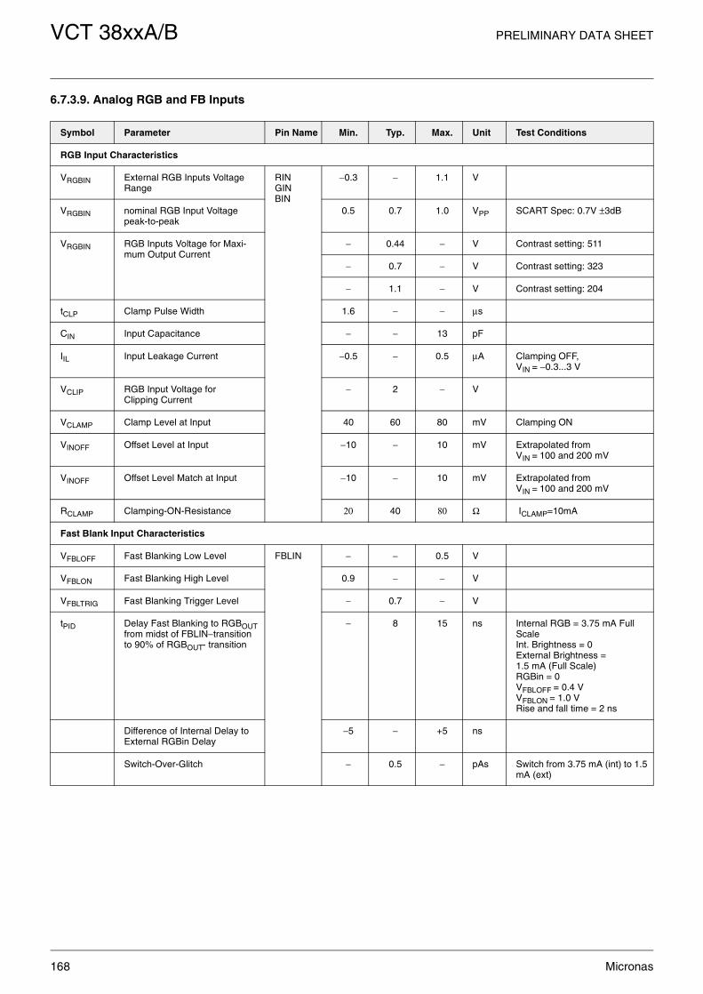
VCT 38xxA/B PRELIMINARY DATA SHEET
168 Micronas
6.7.3.9. Analog RGB and FB Inputs
Symbol Parameter Pin Name Min. Typ. Max. Unit Test Conditions
RGB Input Characteristics
VRGBIN External RGB Inputs Voltage Range
RINGINBIN
−0.3 − 1.1 V
VRGBIN nominal RGB Input Voltage peak-to-peak
0.5 0.7 1.0 VPP SCART Spec: 0.7V ±3dB
VRGBIN RGB Inputs Voltage for Maxi-mum Output Current
− 0.44 − V Contrast setting: 511
− 0.7 − V Contrast setting: 323
− 1.1 − V Contrast setting: 204
tCLP Clamp Pulse Width 1.6 − − µs
CIN Input Capacitance − − 13 pF
IIL Input Leakage Current −0.5 − 0.5 µA Clamping OFF, VIN = −0.3...3 V
VCLIP RGB Input Voltage forClipping Current
− 2 − V
VCLAMP Clamp Level at Input 40 60 80 mV Clamping ON
VINOFF Offset Level at Input −10 − 10 mV Extrapolated from VIN = 100 and 200 mV
VINOFF Offset Level Match at Input −10 − 10 mV Extrapolated from VIN = 100 and 200 mV
RCLAMP Clamping-ON-Resistance 20 40 80 Ω ICLAMP=10mA
Fast Blank Input Characteristics
VFBLOFF Fast Blanking Low Level FBLIN − − 0.5 V
VFBLON Fast Blanking High Level 0.9 − − V
VFBLTRIG Fast Blanking Trigger Level − 0.7 − V
tPID Delay Fast Blanking to RGBOUTfrom midst of FBLIN−transitionto 90% of RGBOUT- transition
− 8 15 ns Internal RGB = 3.75 mA Full ScaleInt. Brightness = 0External Brightness = 1.5 mA (Full Scale)RGBin = 0VFBLOFF = 0.4 VVFBLON = 1.0 VRise and fall time = 2 ns
Difference of Internal Delay to External RGBin Delay
−5 − +5 ns
Switch-Over-Glitch − 0.5 − pAs Switch from 3.75 mA (int) to 1.5 mA (ext)
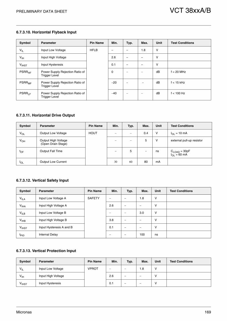
PRELIMINARY DATA SHEET VCT 38xxA/B
Micronas 169
6.7.3.10. Horizontal Flyback Input
6.7.3.11. Horizontal Drive Output
6.7.3.12. Vertical Safety Input
6.7.3.13. Vertical Protection Input
Symbol Parameter Pin Name Min. Typ. Max. Unit Test Conditions
VIL Input Low Voltage HFLB – – 1.8 V
VIH Input High Voltage 2.6 – – V
VIHST Input Hysteresis 0.1 – – V
PSRRHF Power Supply Rejection Ratio of Trigger Level
0 − − dB f = 20 MHz
PSRRMF Power Supply Rejection Ratio of Trigger Level
−20 − − dB f < 15 kHz
PSRRLF Power Supply Rejection Ratio of Trigger Level
−40 − − dB f < 100 Hz
Symbol Parameter Pin Name Min. Typ. Max. Unit Test Conditions
VOL Output Low Voltage HOUT − − 0.4 V IOL = 10 mA
VOH Output High Voltage (Open Drain Stage)
− − 5 V external pull-up resistor
tOF Output Fall Time − 5 - ns CLOAD = 30pFIOL = 60 mA
IOL Output Low Current 30 60 80 mA
Symbol Parameter Pin Name Min. Typ. Max. Unit Test Conditions
VILA Input Low Voltage A SAFETY − − 1.8 V
VIHA Input High Voltage A 2.6 − − V
VILB Input Low Voltage B − − 3.0 V
VIHB Input High Voltage B 3.8 − − V
VIHST Input Hysteresis A and B 0.1 − − V
tPID Internal Delay − − 100 ns
Symbol Parameter Pin Name Min. Typ. Max. Unit Test Conditions
VIL Input Low Voltage VPROT − − 1.8 V
VIH Input High Voltage 2.6 − − V
VIHST Input Hysteresis 0.1 − − V

VCT 38xxA/B PRELIMINARY DATA SHEET
170 Micronas
6.7.3.14. Vertical and East/West D/A Converter Output
6.7.3.15. Interlace Output
6.7.3.16. Sense A/D Converter Input
6.7.3.17. Range Switch Output
Symbol Parameter Pin Name Min. Typ. Max. Unit Test Conditions
VOMIN Minimum Output Voltage EWVERTVERTQ
− 0 − V Rload = 6.8 kΩRxref = 10 kΩ
VOMAX Maximum Output Voltage 2.82 3 3.2 V Rload = 6.8 kΩRxref = 10 kΩ
IDACN Full scale DAC Output Current
415 440 465 µA Rxref = 10 kΩ
PSRR Power Supply Rejection Ratio
− 20 − dB
Symbol Parameter Pin Name Min. Typ. Max. Unit Test Conditions
VOL Output Low Voltage INTLC − 0.2 0.4 V IOL = 1.6 mA
VOH Output High Voltage VSUPAB − 0.4
VSUPAB − 0.2
− V −IOL = 1.6mA
Symbol Parameter Pin Name Min. Typ. Max. Unit Test Conditions
VI Input Voltage Range SENSE 0 − VSUPAB
V
VI255 Input Voltage for code 255 1.4 1.54 1.7 V Read cutoff blue register
C0 Digital Output for zero Input − − 16 LSB Offset check,read cutoff blue register
RI Input Impedance 1 − − MΩ
Symbol Parameter Pin Name Min. Typ. Max. Unit Test Conditions
RON Output On Resistance RSW1RSW2
− 12 25 Ω IOL = 10 mA
IMax Maximum Current − − 15 mA
ILEAK Leakage Current − − 600 nA RSW High Impedance
CIN Input Capacitance − − 5 pF

PRELIMINARY DATA SHEET VCT 38xxA/B
Micronas 171
6.7.3.18. D/A Converter Reference
6.7.3.19. Analog RGB Outputs, D/A Converters
Symbol Parameter Pin Name Min. Typ. Max. Unit Test Conditions
VDACREF DAC-Ref. Voltage VRD 2.38 2.50 2.67 V
VDACR DAC-Ref. Output resistance
18 25 32 kΩ
VXREF DAC-Ref. VoltageBias Current Generation
XREF 2.38 2.5 2.67 V Rxref = 10 kΩ
Symbol Parameter Pin Name Min. Typ. Max. Unit Test Conditions
Internal RGB Signal D/A Converter Characteristics
Resolution ROUTGOUTBOUT
− 10 − bit
IOUT Full Scale Output Current 3.6 3.75 3.9 mA Rref = 10 kΩ
IOUT Differential Nonlinearity − − 0.5 LSB
IOUT Integral Nonlinearity − − 1 LSB
IOUT Glitch Pulse Charge − 0.5 − pAs Ramp signal, 25 Ω output ter-mination
IOUT Rise and Fall Time − 3 − ns 10% to 90%, 90% to 10%
IOUT Intermodulation − − −50 dB 2/2.5MHz full scale
IOUT Signal to Noise +50 − − dB Signal: 1MHz full scale Band-width: 10MHz
IOUT Matching R-G, R-B, G-B −2 − 2 %
R/B/G Crosstalkone channel talks two channels talk
− − −46 dB Passive channel: IOUT =1.88 mACrosstalk-Signal: 1.25 MHz, 3.75 mAPP
RGB Input Crosstalk from exter-nal RGBone channel talks two channels talkthree channels talk
−−−
−−−
−50−50−50
dBdBdB
Internal RGB Brightness D/A Converter Characteristics
Resolution ROUTGOUTBOUT
− 9 − bit
IBR Full Scale Output Current rela-tive
39.2 40 40.8 % Ref to max. digital RGB
IBR Full Scale Output Current abso-lute
− 1.5 − mA
IBR Differential Nonlinearity − − 1 LSB
IBR Integral Nonlinearity − − 2 LSB
IBR Match R-G, R-B, G-B −2 − 2 %
IBR Match to digital RGB R-R, G-G, B-B
−2 − 2 %

VCT 38xxA/B PRELIMINARY DATA SHEET
172 Micronas
External RGB Voltage/Current Converter Characteristics
Resolution ROUTGOUTBOUT
− 9 − bit
IEXOUT Full Scale Output Current rela-tive
96 100 104 % Ref. to max. Digital RGB VIN = 0.7 VPP, contrast = 323
Full Scale Output Currentabsolute
− 3.75 − mA Same as Digital RGB
CR Contrast Adjust Range − 16:511 −
Gain Match R-G, R-B, G-B −3 − 3 % Measured at RGB Outputs VIN = 0.7 V, contrast = 323
Gain Match to RGB-DACsR-R, G-G, B-B
−3 − 3 % Measured at RGB Outputs VIN = 0.7 V, contrast = 323
R/B/G Input Crosstalkone channel talks two channels talk
− − −46 dB Passive channel:VIN = 0.7V, contrast = 323 Crosstalk signal: 1.25 MHz, 3.75 mAPP
RGB Input Crosstalk fromInternal RGBone channel talks two channels talktree channels talk
− − −50 dB
RGB Input Noise and Distortion
− − −50 dB VIN=0.7 VPP at 1 MHz contrast = 323 Bandwidth: 10 MHz
RGB Input Bandwidth -3dB 15 − MHz VIN = 0.7 VPP,contrast =323
RGB Input THD −−
−50−40
−−
dBdB
Input signal 1 MHzInput signal 6 MHzVIN = 0.7 VPPcontrast =323
Differential Nonlinearity ofContrast Adjust
− − 1 LSB VIN = 0.44V
Integral Nonlinearity ofContrast Adjust
− − 2 LSB
VRGBO R,G,B Output Voltage −1.0 − 0.3 V Referred to VSUPO
R,G,B Output Load Resistance − − 100 Ω Ref. to VSUPO
VOUTC RGB Output Compliance −1.5 −1.3 −1.2 V Ref. to VSUPO Sum of max. Current of RGB-DACs and max. Current of Int. Bright-ness DACs is 2% degraded
Symbol Parameter Pin Name Min. Typ. Max. Unit Test Conditions

PRELIMINARY DATA SHEET VCT 38xxA/B
Micronas 173
External RGB Brightness D/A Converter Characteristics
Resolution ROUTGOUTBOUT
− 9 − bit
IEXBR Full Scale Output Current rela-tive
39.2 40 40.8 % Ref to max. digital RGB
Full Scale Output Current abso-lute
− 1.5 − mA
Differential Nonlinearity − − 1 LSB
Integral Nonlinearity − − 2 LSB
Matching R-G, R-B, G-B −2 − 2 %
Matching to digital RGB R-R, G-G, B-B
−2 − 2 %
RGB Output Cutoff D/A Converter Characteristics
Resolution ROUTGOUTBOUT
− 9 − bit
ICUT Full Scale Output Current rela-tive
58.8 60 61.2 % Ref to max. digital RGB
Full Scale Output Current abso-lute
− 2.25 − mA
Differential nonlinearity − − 1 LSB
Integral nonlinearity − − 2 LSB
Matching to digital RGB R-R, G-G, B-B
−2 − 2 %
RGB Output Ultrablack D/A Converter Characteristics
Resolution ROUTGOUTBOUT
− 1 − bit
IUB Full Scale Output Currentrelative
19.6 20 20.4 % Ref to max. digital RGB
Full Scale Output Currentabsolute
− 0.75 − mA
Match to digital RGBR−R, G−G, B−B
−2 − 2 %
Symbol Parameter Pin Name Min. Typ. Max. Unit Test Conditions

VCT 38xxA/B PRELIMINARY DATA SHEET
174 Micronas
6.7.3.20. Scan Velocity Modulation Output
6.7.3.21. Analog Audio Inputs and Outputs
Symbol Parameter Pin Name Min. Typ. Max. Unit Test Conditions
Resolution SVMOUT − 8 − bit
IOUT Full Scale Output Current 1.55 1.875 2.25 mA
IOUT Differential Nonlinearity − − 0.5 LSB
IOUT Integral Nonlinearity − − 1 LSB
IOUT Glitch Pulse Charge − 0.5 − pAs Ramp, output line is termi-nated on both ends with 50 Ω
IOUT Rise and Fall Time − 3 − ns 10% to 90%, 90% to 10%
Symbol Parameter Pin Name Min. Typ. Max. Unit Test Conditions
RAIN Audio Input Resistance AIN1-3AOUT1-2
25 40 58 kΩ fsignal = 1 kHz, I = 0.05 mA
dVAOUT Deviation of DC-Level at Audio Output from GNDAB Voltage
−20 − +20 mV
AAudio Gain from Audio Input to Audio Output
−1.0 0.0 +0.5 dB fsignal = 1 kHzAVOL = 0dB
frAudio Frequency Response from Audio Input to Audio Output bandwidth: 50 Hz to 15000 Hz
−0.5 0.0 +0.5 dB with ρεσπ. to 1 kHz
PSRR Power Supply Rejection Ratio for Audio Output
tbd 50 − dB 1 kHz sine at 100 mVRMS
tbd 20 − dB ≤ 100 kHz sine at 100 mVRMS
VNOISE Noise Output Voltage − tbd 20 µV RGEN = 1kΩ, equally weighted 50 Hz...15 kHz
VMute Mute Output Voltage − tbd 2 µV AVOL = mute, equally weighted 50 Hz...15 kHz
THD Total Harmonic Distortion from Audio Input to Audio Output
− − 0.1 % Input Level = 0.7VRMS,fsig = 1 kHz, equally weighted 50 Hz...15 kHz
XTALK Crosstalk attenuation between Audio Input and Audio Output
70 − − dB Input Level = 0.7VRMS, fsig = 1 kHz, equally weighted50 Hz...15 kHz,unused analog inputs connected to ground by Z < 1 kΩ

PRELIMINARY DATA SHEET VCT 38xxA/B
Micronas 175
6.7.3.22. ADC Input Port
6.7.3.23. Universal Port & Memory Interface
Symbol Parameter Pin Name Min. Typ. Max. Unit Test Conditions
VREF ADC Comparator Reference Voltage
Px.y − 0.5*VSUPS
− V
Vlh−Vhl
ADC Comparator Hysteresis, symmetrical to VREF
0.1 0.17 0.24 V
tCDEL ADC Comparator Delay Time − − 100 ns Overdrive=50mV
LSB LSB Value − VSUPS/1024
− V
R Conversion Range GNDS − VSUPS V
A Conversion Result − INT(Vin/LSB)
− hex GNDS<Vin<VSUPS
000 − − hex Vin<=GNDS
− − 3FF hex Vin>=VSUPS
tc Conversion Time − 4 − µs
ts Sample Time − 2 − µs
DNL Differential Non-Linearity −3 − 3 LSB
INL Integral Non-Linearity −4 − 4 LSB
OFFSET Offset Error −16 − 16 LSB
Ci Input Capacitance during Sam-pling Period
− 15 − pF
Ri Serial Input Resistance during Sampling Period
− 5 − kΩ
Symbol Parameter Pin Name Min. Typ. Max. Unit Test Conditions
Vol Output Low Voltage P1xP2xP3xADB[18-0]DB[7:0]OE1QOE2QWE1QWE2Q
− − 0.41.0
V Io=3mAIo=10mA
Voh Output High Voltage VSUPP−0.4VSUPP−1.5
− − V Io=−3mAIo=−10mA
VIL Input Low Voltage P1xP2xP3xP42−P46DB[7:0]
− − 0.8 V
VIH Input High Voltage 2.0 − − V
Ii Input Leakage Current −1.0 − 1.0 µA 0<Vi<VSUPP

VCT 38xxA/B PRELIMINARY DATA SHEET
176 Micronas
6.7.3.24. Memory Interface
Fig. 6–32: Memory port timing
Symbol Parameter Pin Name Min. Typ. Max. Unit Test Conditions
tCYC PH2 Cycle Time − 98.77 − ns
tADS Address Setup Time ADB[18−0] − 15+ 0.52030
19+ 0.72640
nsns/pfnsns
CADB = 0 pF
CADB = 10 pFCADB = 30 pF
tADH Address Hold Time − 8 10 ns CADB = 10 pF
tDWS Data Write Setup Time DB[7:0] − 9+ 0.51424
14+ 0.72135
nsns/ pFnsns
CDB = 0 pF
CDB = 10 pFCDB = 30 pF
tDWH Data Write Hold Time − 6 8 ns CDB = 0 pF
tDRS Data Read Setup Time 12 − − ns
tDRH Data Read Hold Time 6 − − ns
tENS Enable Setup Time OE1QOE2QWE1QWE2Q
− 6 10 ns COEQ,WEQ = 0 pF
tENH Enable Hold Time − 6 9 ns COEQ,WEQ = 0 pF
PH2
DB[7:0]
DB[7:0] WRITE DATA
READ DATA
ADB[18:0]
tADH
tADS
tACC
tDRStDRH
tDWH tDWS
tENHtENSWEQ,OEQ
tcyc

PRELIMINARY DATA SHEET VCT 38xxA/B
Micronas 177
7. Application
Fig. 7–1: VCT 38xxA/B application circuit, part 1/3

VCT 38xxA/B PRELIMINARY DATA SHEET
178 Micronas
Fig. 7–2: VCT 38xxA/B application circuit, part 2/3

PRELIMINARY DATA SHEET VCT 38xxA/B
Micronas 179
Fig. 7–3: VCT 38xxA/B application circuit, part 3/3
VCT 38xxA/B PRELIMINARY DATA SHEET
180 Micronas
8. Glossary of Abbreviations
AIT Additional Information Table
BTT Basic TOP Table
BTTL Basic TOP Table List
CCU Central Control Unit
CLUT Color Look Up Table
CPU Central Processing Unit
CRI Clock Running-in
DMA Direct Memory Access
DRAM Dynamic Random Access Memory
FLOF Full Level One Features
FRC Framing Code
MPT Multipage Table
MPET Multipage Extension Table
NMI Non Maskable Interrupt
OSD On Screen Display
PDC Programme Delivery Control
PLT Page Linking Table
RAM Random Access Memory
ROM Read Only Memory
SRAM Static Random Access Memory
TOP Table Of Pages
TPU Teletext Processing Unit
TTX Teletext
VBI Vertical Blanking Interval
VPS Video-Programm-System
WSS Wide Screen Signalling
WST World System Teletext
9. References
1. Preliminary Data Sheet: “VDP 31xxB”, Sept. 25, 19986251-437-2PD
2. Preliminary Data Sheet: “TPU 3035, TPU 3040, TPU 3050”, Feb. 23, 19996251-349-6PD
3. Preliminary Data Sheet: “W65C02”, Oct. 2, 19916251-364-1PD
4.“Enhanced Teletext Specification”. European Telecommunication Standard ETS 300 706. ETSI, May1997.
5. “Television systems; 625-line television Wide Screen Signalling (WSS)”. European Telecommuni-cation Standard ETS 300 294. ETSI, May1996.
6. “Television systems; Specification of the domestic video Programme Delivery Control system (PDC)”. European Telecommunication Standard ETS 300 231. ETSI, August1996.
7. “Electronic Programme Guide (EPG)”. European Telecommunication Standard ETS 300 707. ETSI, May1997.

PRELIMINARY DATA SHEET VCT 38xxA/B
Micronas 181
All information and data contained in this data sheet are without anycommitment, are not to be considered as an offer for conclusion of acontract, nor shall they be construed as to create any liability. Any newissue of this data sheet invalidates previous issues. Product availabilityand delivery are exclusively subject to our respective order confirmationform; the same applies to orders based on development samples deliv-ered. By this publication, Micronas GmbH does not assume responsibil-ity for patent infringements or other rights of third parties which mayresult from its use.Further, Micronas GmbH reserves the right to revise this publicationand to make changes to its content, at any time, without obligation tonotify any person or entity of such revisions or changes. No part of this publication may be reproduced, photocopied, stored on aretrieval system, or transmitted without the express written consent ofMicronas GmbH.
VCT 38xxA/B PRELIMINARY DATA SHEET
182 Micronas
Micronas GmbHHans-Bunte-Strasse 19D-79108 Freiburg (Germany)P.O. Box 840D-79008 Freiburg (Germany)Tel. +49-761-517-0Fax +49-761-517-2174E-mail: [email protected]: www.micronas.com
Printed in GermanyOrder No. 6251-518-1PD
10. Data Sheet History
1. Preliminary data sheet: “VCT 38xxA/B Video/Con-troller/Teletext IC Family”, Edition Jan. 8, 2002, 6251-518-1PD. First release of the preliminary data sheet.