microprocessors and interfacing (a1423) unit i introduction · microprocessors and interfacing...
TRANSCRIPT

2/20/2015
1
Department of Electronics and Communication Engineering
VARDHAMAN COLLEGE OF ENGINEERING
Shamshabad, Hyderabad – 501218, India.
Microprocessors and Interfacing (A1423)Unit – I Introduction
Microprocessors and Interfacing (A1423)
Pre-requisites
Digital Logic Design (A1404)
Computer Architecture and Organization (A1509)
20 February 20152

2/20/2015
2
Microprocessors and Interfacing (A1423)
Douglas V. Hall (2007), Microprocessors and Interfacing
Programming and Hardware, 2nd Edition, Tata McGraw Hill,
New Delhi.
A. K. Ray, K. M. Bhurchandi, Advanced Microprocessors
and Peripherals, 2nd Edition, Tata McGraw Hill, New Delhi.
Text Books
20 February 20153
Microprocessors and Interfacing (A1423)
Reference Books
Walter A. Triebel, Avtar Singh (2003), The 8088 and 8086
Microprocessors, 4th Edition, Prentice Hall of India, New
Delhi.
Barry B. Brey (2001), The Intel Microprocessors
8086/8088, 80186/80188, 80286, 80386, 80486, Pentium,
and Pentium Pro Processor, Architecture, Programming,
and Interfacing, 4th Edition, Prentice Hall of India, New
Delhi.
Kenneth J. Ayala (2008), The 8086 Microprocessor:
Programming & Interfacing the PC, Cengage Learning,
New Delhi.
20 February 20154
2/20/2015
3
Microprocessors and Interfacing (A1423)
Unit - I
Number Systems and Digital Logic Review
Overview of Microcomputer Structure and Operation
Evolution of Microprocessors
8086 Microprocessor Architecture
Register Organization
8086 Pin Diagram and Signal Description
8086 Minimum Mode and Its Timing Diagram
8086 Maximum Mode and Its Timing Diagram
Addressing Modes
20 February 20155
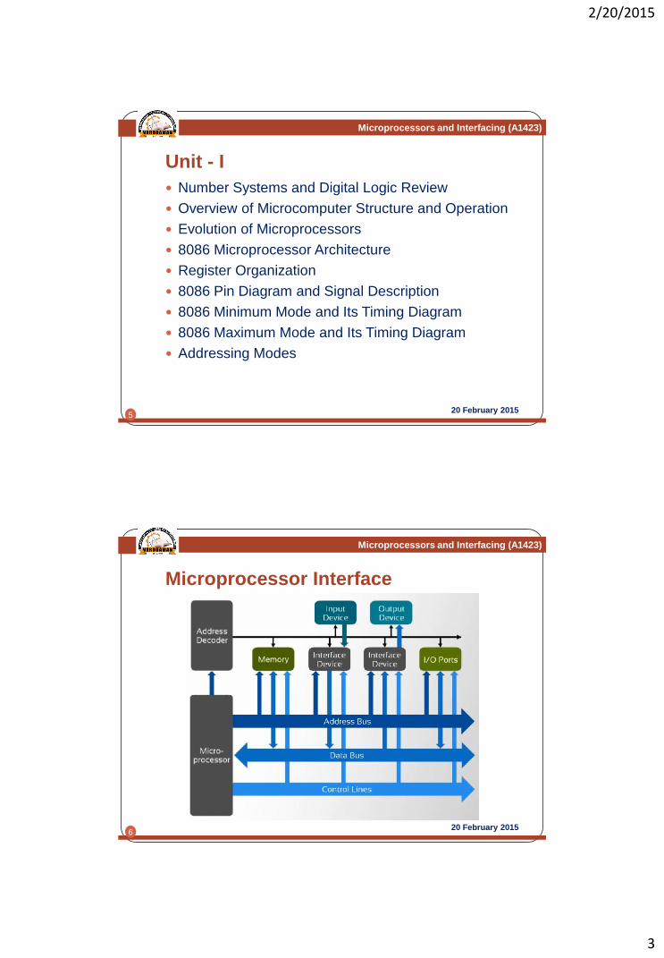
Microprocessors and Interfacing (A1423)
Microprocessor Interface
20 February 20156

2/20/2015
4
Microprocessors and Interfacing (A1423)
Evolution of Microprocessors
20 February 20157
Based on the Word Length (Number of binary bits in dataprocessing)
4-bit, 8-bit, 16-bit, 32-bit, and 64-bit
4004
8008
8080
8085
8086
80286
80386
Pentium
Pentium Pro
Microprocessors and Interfacing (A1423)
INTEL 4004
Built in 1971
4 Bit Micro-processor
Initial clock speed 108 KHz
No of transistors used 2300
Developed on P-MOS technology

2/20/2015
5
Microprocessors and Interfacing (A1423)
INTEL 8008
1) Built in 1972
2) 8 bit Micro-processor
3) Initial clock speed of 500-800 KHz
4) No of transistors used were 3500
5) Also developed on PMOS technology
Microprocessors and Interfacing (A1423)
INTEL 8080
1) Built in 1974
2) 8 Bit Microprocessor
3) Initial clock speed 500-800 KHz
4) No of transistors used 4500
5) Developed using NMOS Technology
6) Drawbacks: It required 3 power supplies

2/20/2015
6
Microprocessors and Interfacing (A1423)
INTEL 80851) Built in 1977
2) 5 in 8085 means +5 volt supply
3) Initial clock speed of about 3MHz
4) Approx. 6500 transistors were used
5) 8 Bit µ-Processor using NMOS technology
SPECIAL FEATURES
1) Extension to support new interrupts :- Maskable (RST 7.5,RST 6.5,RST 5.5) Non-Maskable (TRAP) and externally serviced Interrupt (INTR).
2) 8085 can itself drive piezoelectric crystal directly connected to it.
3) Through 8 bit Microprocessor but it can also load 16 bit data
(Through pairs BC DE HL).
Microprocessors and Interfacing (A1423)
INTEL 80861) Built in 1979
2) 16 bit Microprocessor
3) It has 20 bit address bus and 1 MB addressing space
4) Initial clock speed of 5 MHz,8 MHz and 10 MHz
5) No of transistors used were 29,000
SPECIAL FEATURES
1) Memory divided into odd and even banks
2) Can read upto 16 bits of data in one cycle

2/20/2015
7
Microprocessors and Interfacing (A1423)
INTEL 80286 Processor1) It is a 16 bit x86
processor
2) Provides Memory management & protection
3) Initial clock speed 8 MHz
4) 24 bit address bus gives the capacity to access 16 MB storage
5) About 134,000transistors were used
INTEL 80386 Processor1) It is a 32 bit x86
processor
2) It has 32 bit address bus and 32 bit data bus
3) Clock speeds between 12-40 MHz
4) It can access upto 4GB of physical memory
5) About 275,000 transistors were used
Microprocessors and Interfacing (A1423)
Intel Pentium Processor:-1) Built in 1993
2) Clock speed 66 MHz
3) Approx. 31 Lakhs transistors were used
4) 112 million commands per second could be executed per second.
Pentium Series Advancement:-(Pentium 2 to Pentium 4 processor)1) Clock speed was increased from 66 MHz to 1.7 GHz
2) No of transistors were also increased from 31 Lakhs to 5.5 Crore

2/20/2015
8
Microprocessors and Interfacing (A1423)
INTEL CORE 2 DUO AND DUAL CORE
PROCESSORS:-1) Built in 2006 and 2007 respectively
2) Clock speed varies from 1.6 GHz to 2.6 Ghz
3) In built cache memory of 2MB to 6 MB
4) Both are 64 bit microprocessors
5) Both were mainly media centred and provided HD
display quality

2/20/2015
9
Microprocessors and Interfacing (A1423)
INTEL CORE SERIES (i3,i5,i7, i7
extreme)
1) Core are more powerful variants of the same
processors sold as Celeron and Pentium
2) They are made mainly for multitasking
3) These processors were made available to public
from January 2010
4) Clock speed varies from 1.7GHz (slowest) and
3.5GHz (fastest)
Microprocessors and Interfacing (A1423)
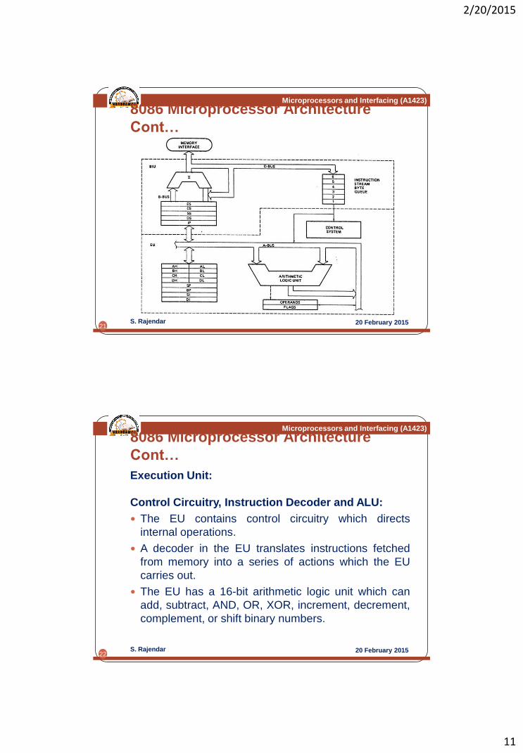
8086 Microprocessor Architecture
The architecture of 8086 microprocessor
supports/provides
• a 16-bit ALU
• a set of 16-bit registers
• segmented memory addressing capability
• a rich instruction set
• powerful interrupt structure
• fetched instruction queue for overlapped fetching
and execution etc.
20 February 201518
S. Rajendar

2/20/2015
10
Microprocessors and Interfacing (A1423)
8086 Microprocessor Architecture
Cont…
To improve the performance by implementing the
parallel processing concept the CPU of the 8086 is
divided into two independent sections.
They are
• Bus Interface Unit (BIU) and
• Execution Unit (EU)
The BIU sends out addresses, fetches instructions,
read data from ports and memory and writes data to
ports and memory, i.e., the BIU handles all transfers
of data and addresses on the buses required by the
Execution Unit whereas the Execution Unit tells the
BIU where to fetch instructions or data from, decodes
the instructions and executes the instructions.20 February 2015
19S. Rajendar
Microprocessors and Interfacing (A1423)
8086 Microprocessor Architecture
Cont…
The BIU contains• the circuit for physical address calculations• a predecoding instruction byte queue (6 bytes
long)• four 16-bit segment registers (ES, CS, SS, DS)• 16-bit instruction pointer (IP)
The EU contains• control circuitry, instruction decoder and ALU• 16-bit flag registers• four 16-bit general purpose registers (AX, BX,
CX, DX)• 16-bit pointer registers (SP, BP) and • 16-bit index registers (SI, DI)
20 February 201520
S. Rajendar
2/20/2015
11
Microprocessors and Interfacing (A1423)
8086 Microprocessor Architecture
Cont…
20 February 201521
S. Rajendar
Microprocessors and Interfacing (A1423)
8086 Microprocessor Architecture
Cont…
Execution Unit:
Control Circuitry, Instruction Decoder and ALU:
The EU contains control circuitry which directs
internal operations.
A decoder in the EU translates instructions fetched
from memory into a series of actions which the EU
carries out.
The EU has a 16-bit arithmetic logic unit which can
add, subtract, AND, OR, XOR, increment, decrement,
complement, or shift binary numbers.
20 February 201522
S. Rajendar
2/20/2015
12
Microprocessors and Interfacing (A1423)
8086 Microprocessor Architecture
Cont…
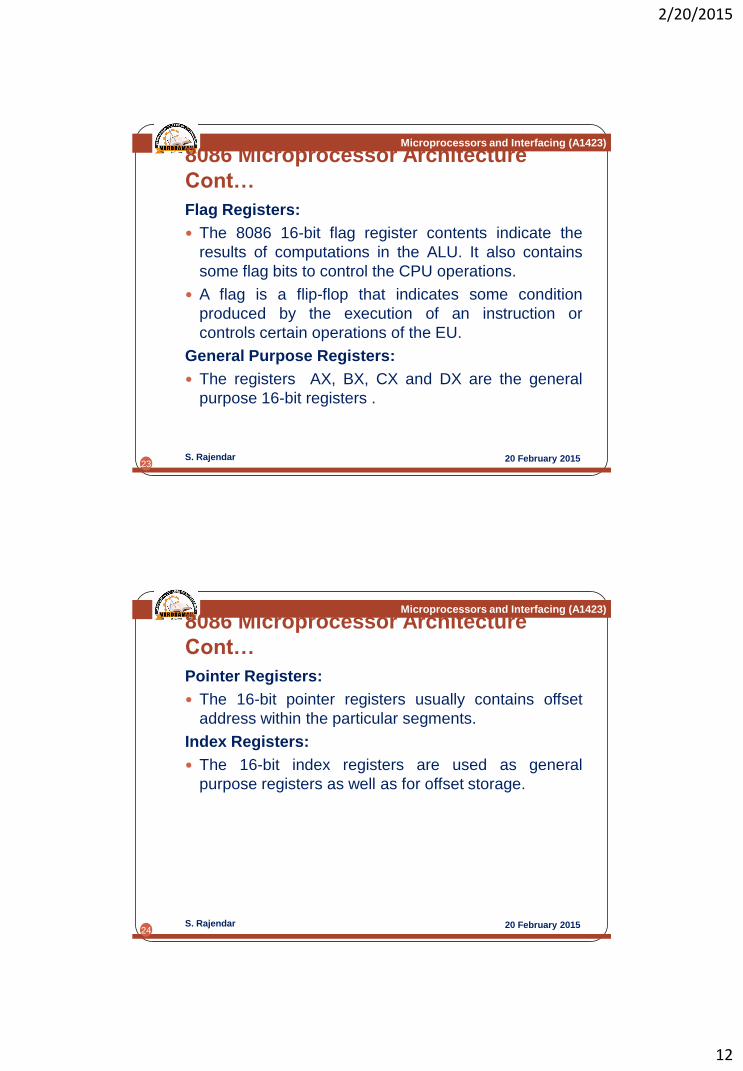
Flag Registers:
The 8086 16-bit flag register contents indicate the
results of computations in the ALU. It also contains
some flag bits to control the CPU operations.
A flag is a flip-flop that indicates some condition
produced by the execution of an instruction or
controls certain operations of the EU.
General Purpose Registers:
The registers AX, BX, CX and DX are the general
purpose 16-bit registers .
20 February 201523
S. Rajendar
Microprocessors and Interfacing (A1423)
8086 Microprocessor Architecture
Cont…
Pointer Registers:
The 16-bit pointer registers usually contains offset
address within the particular segments.
Index Registers:
The 16-bit index registers are used as general
purpose registers as well as for offset storage.
20 February 201524
S. Rajendar

2/20/2015
13
Microprocessors and Interfacing (A1423)
8086 Microprocessor Architecture
Cont…Bus Interface Unit:
The Queue:
While the EU is decoding an instruction or executing aninstruction which does not require use of the buses, the BIUfetches up to six instruction bytes for the following instructions.
The BIU stores these prefetched bytes in a first-in-first-outregister set called a queue.
When the EU is ready for its next instruction, it simply reads theinstruction byte(s) for the instruction from the queue in the BIU.
This is much faster than sending out an address to the systemmemory and waiting for memory to send back the nextinstruction byte or bytes.
Fetching the next instruction while the current instructionexecutes is called pipelining.
20 February 201525
S. Rajendar
Microprocessors and Interfacing (A1423)
8086 Microprocessor Architecture
Cont…
Segment Registers:
The 8086 BIU sends out 20-bit addresses, so it can
address any of 220 or 1,048,576 bytes in memory.
However, at any given time the 8086 works with only four
65,536 byte (64Kbyte) segments within this 1,048,576 byte
(1 Mbyte) range.
Four segment registers in the BIU are used to hold the
upper 16 bits of the starting addresses of four memory
segments that the 8086 is working with at a particular time.
The four segment registers are the code segment (CS)
register, the stack segment (SS) register, the extra
segment (ES) register, and the data segment (DS) register.
20 February 201526
S. Rajendar

2/20/2015
14
Microprocessors and Interfacing (A1423)
8086 Microprocessor Architecture
Cont…
Instruction Pointer:
The instruction pointer register holds the 16-bit
addresses, or offset, of the next code byte within this
code segment.
20 February 201527
S. Rajendar
Microprocessors and Interfacing (A1423)
Memory Segmentation:
20 February 201528
S. Rajendar
2/20/2015
15
Microprocessors and Interfacing (A1423)
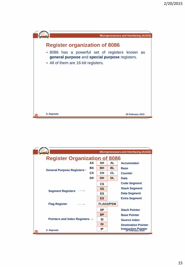
Register organization of 8086
8086 has a powerful set of registers known as
general purpose and special purpose registers.
All of them are 16-bit registers.
20 February 201529
S. Rajendar
Microprocessors and Interfacing (A1423)
Register Organization of 8086
20 February 201530
S. Rajendar
CS
SS
DS
ES
SP
BP
SI
DI
IP
FLAGS/PSW
General Purpose Registers
Segment Registers
Flag Register
Pointers and Index Registers
AX AH AL
BX BH BL
CX CH CL
DX DH DL
Accumulator
Base
Counter
Data
Code Segment
Stack Segment
Data Segment
Extra Segment
Stack Pointer
Base Pointer
Source Index
Destination Pointer
Instruction Pointer
2/20/2015
16
Microprocessors and Interfacing (A1423)
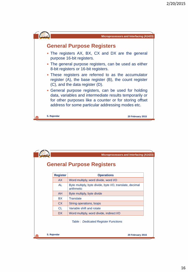
General Purpose Registers
The registers AX, BX, CX and DX are the general
purpose 16-bit registers.
The general purpose registers, can be used as either
8-bit registers or 16-bit registers.
These registers are referred to as the accumulator
register (A), the base register (B), the count register
(C), and the data register (D).
General purpose registers, can be used for holding
data, variables and intermediate results temporarily or
for other purposes like a counter or for storing offset
address for some particular addressing modes etc.
20 February 201531
S. Rajendar
Microprocessors and Interfacing (A1423)
General Purpose Registers
Table : Dedicated Register Functions
20 February 201532
S. Rajendar
Register Operations
AX Word multiply, word divide, word I/O
AL Byte multiply, byte divide, byte I/O, translate, decimal
arithmetic
AH Byte multiply, byte divide
BX Translate
CX String operations, loops
CL Variable shift and rotate
DX Word multiply, word divide, indirect I/O

2/20/2015
17
Microprocessors and Interfacing (A1423)
Special Purpose Registers
Segment Registers
Pointers and Index Registers
Flag Register
The special purpose registers are used as segment
registers, pointers, index registers or as offset storage
registers for particular addressing modes.
20 February 201533
S. Rajendar
Microprocessors and Interfacing (A1423)
Segment Registers
8086 addresses a segmented memory.
The complete 1MB memory, which the 8086
addresses, is divided into 16 logical segments.
Each segment thus contains 64KB of memory.
There are four segment registers, viz.
Code Segment Register (CS)
Data Segment Register (DS)
Extra Segment Register (ES)
Stack Segment Register (SS)
20 February 201534
S. Rajendar
2/20/2015
18
Microprocessors and Interfacing (A1423)
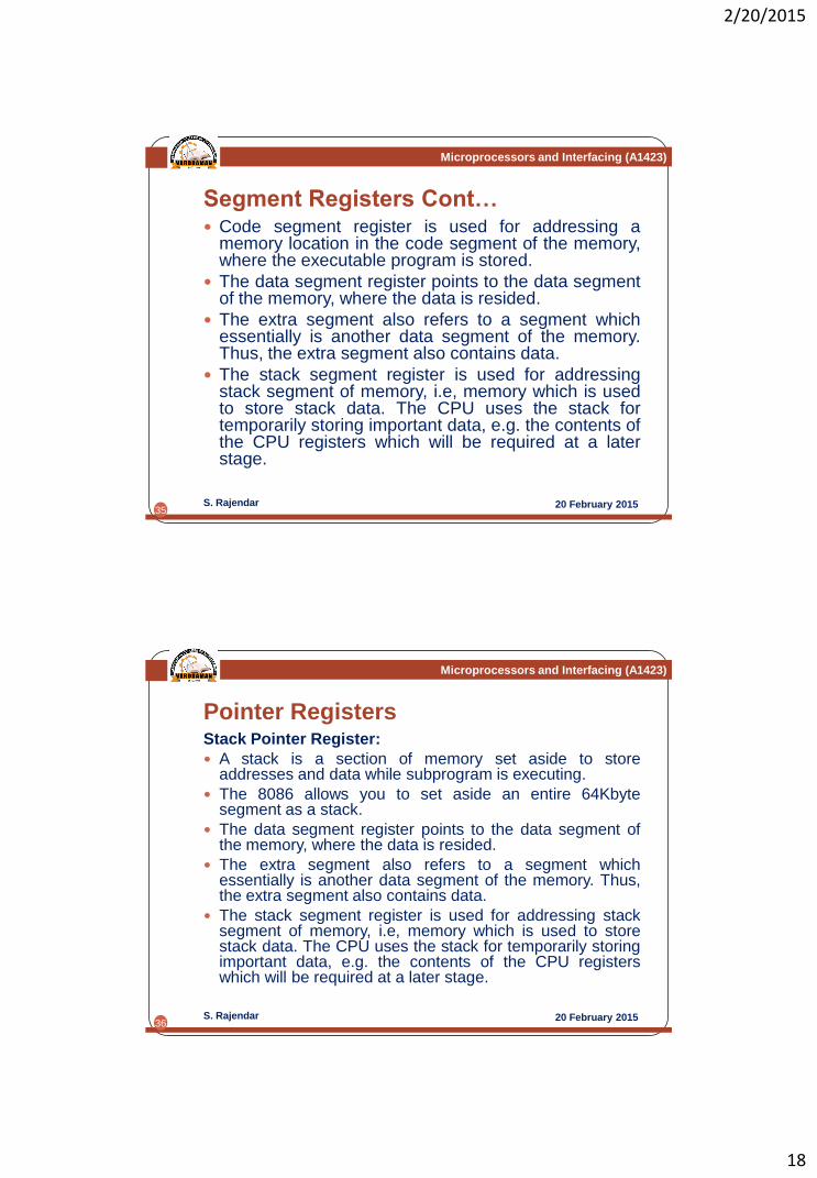
Segment Registers Cont… Code segment register is used for addressing a
memory location in the code segment of the memory,where the executable program is stored.
The data segment register points to the data segmentof the memory, where the data is resided.
The extra segment also refers to a segment whichessentially is another data segment of the memory.Thus, the extra segment also contains data.
The stack segment register is used for addressingstack segment of memory, i.e, memory which is usedto store stack data. The CPU uses the stack fortemporarily storing important data, e.g. the contents ofthe CPU registers which will be required at a laterstage.
20 February 201535
S. Rajendar
Microprocessors and Interfacing (A1423)
Pointer RegistersStack Pointer Register:
A stack is a section of memory set aside to storeaddresses and data while subprogram is executing.
The 8086 allows you to set aside an entire 64Kbytesegment as a stack.
The data segment register points to the data segment ofthe memory, where the data is resided.
The extra segment also refers to a segment whichessentially is another data segment of the memory. Thus,the extra segment also contains data.
The stack segment register is used for addressing stacksegment of memory, i.e, memory which is used to storestack data. The CPU uses the stack for temporarily storingimportant data, e.g. the contents of the CPU registerswhich will be required at a later stage.
20 February 201536
S. Rajendar

2/20/2015
19
Architecture8086 Microprocessor
37
Execution Unit (EU)
EU executes instructions that have already been fetched by the BIU.
BIU and EU functions separately.
Bus Interface Unit (BIU)
BIU fetches instructions, reads data from memory and I/O ports, writes
data to memory and I/ O ports.
Architecture8086 Microprocessor
38
Bus Interface Unit (BIU)
Dedicated Adder to generate 20 bit address
Four 16-bit segment registers
Code Segment (CS)Data Segment (DS)Stack Segment (SS)Extra Segment (ES)
Segment Registers >>

2/20/2015
20
Architecture8086 Microprocessor
39
Bus Interface Unit (BIU)
Segment Registers
8086’s 1-megabytememory is dividedinto segments of upto 64K bytes each.
Programs obtain accessto code and data in thesegments by changingthe segment registercontent to point to thedesired segments.
The 8086 can directlyaddress four segments(256 K bytes within the 1M byte of memory) at aparticular time.
Architecture8086 Microprocessor
40
Bus Interface Unit (BIU)
Segment Registers
Code Segment Register
16-bit
CS contains the base or start of the current code segment; IP contains the distance or offset from this address to the next instruction byte to be fetched.
BIU computes the 20-bit physical address by logically shifting the contents of CS 4-bits to the left and then adding the 16-bit contents of IP.
That is, all instructions of a program are relative to the contents of the CS register multiplied by 16 and then offset is added provided by the IP.
2/20/2015
21
Architecture8086 Microprocessor
41
Bus Interface Unit (BIU)
Segment Registers
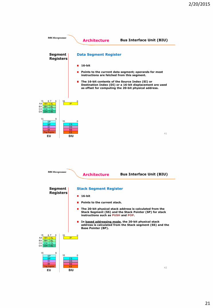
Data Segment Register
16-bit
Points to the current data segment; operands for most instructions are fetched from this segment.
The 16-bit contents of the Source Index (SI) or Destination Index (DI) or a 16-bit displacement are used as offset for computing the 20-bit physical address.
Architecture8086 Microprocessor
42
Bus Interface Unit (BIU)
Segment Registers
Stack Segment Register
16-bit
Points to the current stack.
The 20-bit physical stack address is calculated from the Stack Segment (SS) and the Stack Pointer (SP) for stack instructions such as PUSH and POP.
In based addressing mode, the 20-bit physical stack address is calculated from the Stack segment (SS) and the Base Pointer (BP).

2/20/2015
22
Architecture8086 Microprocessor
43
Bus Interface Unit (BIU)
Segment Registers
Extra Segment Register
16-bit
Points to the extra segment in which data (in excess of 64K pointed to by the DS) is stored.
String instructions use the ES and DI to determine the 20-bit physical address for the destination.
Architecture8086 Microprocessor
44
Bus Interface Unit (BIU)
Segment Registers
Instruction Pointer
16-bit
Always points to the next instruction to be executed withinthe currently executing code segment.
So, this register contains the 16-bit offset address pointingto the next instruction code within the 64Kb of the codesegment area.
Its content is automatically incremented as the executionof the next instruction takes place.

2/20/2015
23
Architecture8086 Microprocessor
45
Bus Interface Unit (BIU)
A group of First-In-First-Out (FIFO) in which up to6 bytes of instructioncode are pre fetchedfrom the memory aheadof time.
This is done in order tospeed up the executionby overlappinginstruction fetch withexecution.
This mechanism is knownas pipelining.
Instruction queue
Architecture8086 Microprocessor
46
Some of the 16 bit registers can be used as two 8 bit registers as :
AX can be used as AH and ALBX can be used as BH and BLCX can be used as CH and CLDX can be used as DH and DL
Execution Unit (EU)
EU decodes and executes instructions.
A decoder in the EU control system
translates instructions.
16-bit ALU forperforming arithmeticand logic operation
Four general purpose registers(AX, BX, CX, DX);
Pointer registers (Stack Pointer, Base Pointer);
and
Index registers (Source Index, Destination Index) each of 16-bits

2/20/2015
24
Architecture8086 Microprocessor
47
EURegisters
Accumulator Register (AX)
Consists of two 8-bit registers AL and AH, which can becombined together and used as a 16-bit register AX.
AL in this case contains the low order byte of the word,and AH contains the high-order byte.
The I/O instructions use the AX or AL for inputting /outputting 16 or 8 bit data to or from an I/O port.
Multiplication and Division instructions also use the AX orAL.
Execution Unit (EU)
Architecture8086 Microprocessor
48
EURegisters
Base Register (BX)
Consists of two 8-bit registers BL and BH, which can becombined together and used as a 16-bit register BX.
BL in this case contains the low-order byte of the word,and BH contains the high-order byte.
This is the only general purpose register whose contentscan be used for addressing the 8086 memory.
All memory references utilizing this register content foraddressing use DS as the default segment register.
Execution Unit (EU)

2/20/2015
25
Architecture8086 Microprocessor
49
EURegisters
Counter Register (CX)
Consists of two 8-bit registers CL and CH, which can becombined together and used as a 16-bit register CX.
When combined, CL register contains the low order byte ofthe word, and CH contains the high-order byte.
Instructions such as SHIFT, ROTATE and LOOP use thecontents of CX as a counter.
Execution Unit (EU)
Example:
The instruction LOOP START automatically decrementsCX by 1 without affecting flags and will check if [CX] =0.
If it is zero, 8086 executes the next instruction;otherwise the 8086 branches to the label START.
Architecture8086 Microprocessor
50
EURegisters
Execution Unit (EU)
2/20/2015
26
Architecture8086 Microprocessor
51
EURegisters
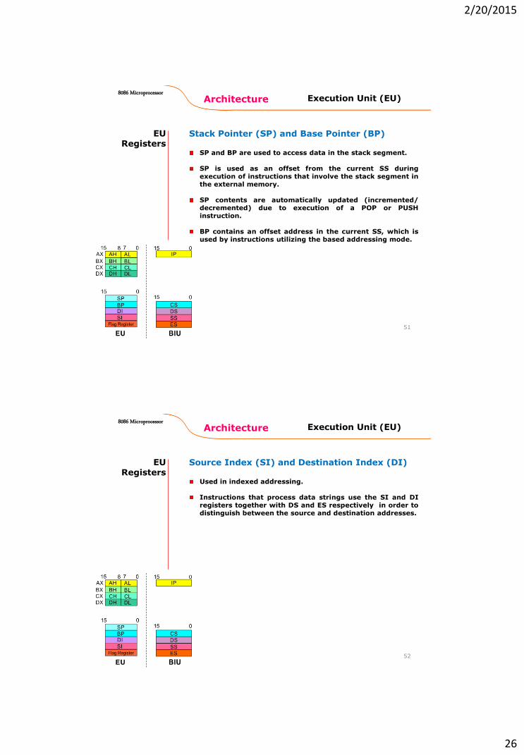
Stack Pointer (SP) and Base Pointer (BP)
SP and BP are used to access data in the stack segment.
SP is used as an offset from the current SS duringexecution of instructions that involve the stack segment inthe external memory.
SP contents are automatically updated (incremented/decremented) due to execution of a POP or PUSHinstruction.
BP contains an offset address in the current SS, which isused by instructions utilizing the based addressing mode.
Execution Unit (EU)
Architecture8086 Microprocessor
52
EURegisters
Source Index (SI) and Destination Index (DI)
Used in indexed addressing.
Instructions that process data strings use the SI and DIregisters together with DS and ES respectively in order todistinguish between the source and destination addresses.
Execution Unit (EU)

2/20/2015
27
Architecture8086 Microprocessor
53
EURegisters
Source Index (SI) and Destination Index (DI)
Used in indexed addressing.
Instructions that process data strings use the SI and DIregisters together with DS and ES respectively in order todistinguish between the source and destination addresses.
Execution Unit (EU)
Microprocessor System Design 3-54
Generating Memory Addresses
How can a 16-bit microprocessor generate 20-bit memory addresses?
Segment
(64K)
0000
+
16-bit register
16-bit register
20-bit memory address
00000
FFFFFLeft shift 4 bits
Intel 80x86 memory address generation 1M memory space
Offset
Segment
address
OffsetAddr1
Addr1 + 0FFFF

2/20/2015
28
Microprocessor System Design 3-55
Memory Segmentation
A segment is a 64KB block of memory starting from any 16-byte
boundary
For example: 00000, 00010, 00020, 20000, 8CE90, and E0840 are all valid
segment addresses
The requirement of starting from 16-byte boundary is due to the 4-bit
left shifting
Segment registers in BIU
CS
SS
DS
ES
Code Segment
Data Segment
Stack Segment
Extra Segment
015
Microprocessor System Design 3-56
Memory Address Calculation
Segment addresses must be stored
in segment registers
Offset is derived from the combination
of pointer registers, the Instruction
Pointer (IP), and immediate values
0000
+
Segment address
Offset
Memory address
Examples
3 4 8 A 0
4 2 1 4
8 A B 43
CS
IP +
Instruction address
5 0 0 0 0
F F E 0
F F E 05
SS
SP +
Stack address
1 2 3 4 0
0 0 2 2
2 3 6 21
DS
DI +
Data address

2/20/2015
29
Architecture8086 Microprocessor
57
Flag Register
15 14 13 12 11 10 9 8 7 6 5 4 3 2 1 0
OF DF IF TF SF ZF AF PF CF
Carry Flag
This flag is set, when there isa carry out of MSB in case ofaddition or a borrow in caseof subtraction.
Parity Flag
This flag is set to 1, if the lowerbyte of the result contains evennumber of 1’s ; for odd numberof 1’s set to zero.
Auxiliary Carry Flag
This is set, if there is a carry from thelowest nibble, i.e, bit three duringaddition, or borrow for the lowestnibble, i.e, bit three, duringsubtraction.
Zero Flag
This flag is set, if the result ofthe computation or comparisonperformed by an instruction iszero
Sign Flag
This flag is set, when the result of any computation
is negative
Tarp FlagIf this flag is set, the processorenters the single step executionmode by generating internalinterrupts after the execution ofeach instruction
Interrupt Flag
Causes the 8086 to recognize external mask interrupts; clearing IF
disables these interrupts.
Direction FlagThis is used by string manipulation instructions. If this flag bitis ‘0’, the string is processed beginning from the lowestaddress to the highest address, i.e., auto incrementing mode.Otherwise, the string is processed from the highest addresstowards the lowest address, i.e., auto incrementing mode.
Over flow FlagThis flag is set, if an overflow occurs, i.e, if the result of a signed
operation is large enough to accommodate in a destination register. The result is of more than 7-bits in size in case of 8-bit signed operation and more than 15-bits in size in case of 16-bit
sign operations, then the overflow will be set.
Execution Unit (EU)
58
Architecture8086 Microprocessor
Sl.No. Type Register width Name of register
1 General purpose register 16 bit AX, BX, CX, DX
8 bit AL, AH, BL, BH, CL, CH, DL, DH
2 Pointer register 16 bit SP, BP
3 Index register 16 bit SI, DI
4 Instruction Pointer 16 bit IP
5 Segment register 16 bit CS, DS, SS, ES
6 Flag (PSW) 16 bit Flag register
8086 registers categorized
into 4 groups
15 14 13 12 11 10 9 8 7 6 5 4 3 2 1 0
OF DF IF TF SF ZF AF PF CF

2/20/2015
30
59
Architecture8086 Microprocessor
Register Name of the Register Special Function
AX 16-bit Accumulator Stores the 16-bit results of arithmetic and logic operations
AL 8-bit Accumulator Stores the 8-bit results of arithmetic and logic operations
BX Base register Used to hold base value in base addressing mode to access memory data
CX Count Register Used to hold the count value in SHIFT, ROTATE and LOOP instructions
DX Data Register Used to hold data for multiplication and division operations
SP Stack Pointer Used to hold the offset address of top stack memory
BP Base Pointer Used to hold the base value in base addressing using SS register to access data from stack memory
SI Source Index Used to hold index value of source operand (data) for string instructions
DI Data Index Used to hold the index value of destination operand (data) for string operations
Registers and Special Functions
Pins and Signals8086 Microprocessor
60
Common signals
AD0-AD15 (Bidirectional)Address/Data bus
These are the time multiplexed memoryI/O address and data lines.Address remains on the lines during T1
state, while the data is available on thedata bus during T2, T3, Tw and T4.Here T1, T2, T3, T4 and Tw are the clockstates of a machine cycle. Tw is a waitstate.These lines are active high and float to atristate during interrupt acknowledgeand local bus hold acknowledge cycles.
A16/S3, A17/S4, A18/S5, A19/S6
These are time multiplexed address andstatus signalsS4,S3 indicates which segment registerbeing used.S5 gives current setting of interrupt flagand S6 is always Low.

2/20/2015
31
Pins and Signals8086 Microprocessor
61
Common signals
BHE (Active Low)/S7 (Output)
Bus High Enable/Status
It is used to enable data onto the mostsignificant half of data bus, D8-D15. 8-bitdevice connected to upper half of thedata bus use BHE (Active Low) signal. Itis multiplexed with status signal S7. S7 isnot currently used.
MN/ MX
MINIMUM / MAXIMUM
This pin signal indicates what mode theprocessor is to operate in, eitherminimum (single processor) or maximum(multiprocessor) mode.
RD (Read) (Active Low)
The signal is used for read (Memory or I/O read) operation. It is an output signal. It is active when low.
Pins and Signals8086 Microprocessor
62
Common signals
READY
This is the acknowledgement from theslow device or memory that they havecompleted the data transfer.
The signal made available by the devicesis synchronized by the 8284A clockgenerator to provide ready input to the8086.
The signal is active high.
TEST (Active Low)
This input is examined by a WAITinstruction.
If the TEST input goes low, execution willcontinue, else, the processor remains inan idle state.
The input is synchronized internallyduring each clock cycle on leading edgeof clock.
The signal is active low.

2/20/2015
32
Pins and Signals8086 Microprocessor
63
Common signals
RESET (Input)
Causes the processor to immediatelyterminate its present activity.
The signal must be active HIGH for atleast four clock cycles.
CLK
The clock input provides the basic timingfor processor operation and bus controlactivity. Its an asymmetric square wavewith 33% duty cycle.
INTR Interrupt Request
This is a level triggered input. This issampled during the last clock cycles ofeach instruction to determine theavailability of the request. If anyinterrupt request is pending, theprocessor enters the interruptacknowledge cycle.
This signal is active high and internallysynchronized.
Pins and Signals8086 Microprocessor
64
Min/ Max Pins
The 8086 microprocessor can work in twomodes of operations : Minimum mode andMaximum mode.
In the minimum mode of operation themicroprocessor do not associate with anyco-processors and can not be used formultiprocessor systems.
In the maximum mode the 8086 can workin multi-processor or co-processorconfiguration.
Minimum or maximum mode operationsare decided by the pin MN/ MX(Active low).
When this pin is high 8086 operates inminimum mode otherwise it operates inMaximum mode.

2/20/2015
33
Pins and Signals8086 Microprocessor
(Data Transmit/ Receive) Output signal from the processor to control the direction of data flow through the data transceivers
(Data Enable) Output signal from the processor used as out put enable for the transceivers
ALE (Address Latch Enable) Used to demultiplex the address and data lines using external latches
Used to differentiate memory access and I/O access. For memory reference instructions, it is high. For IN and OUT instructions, it is low.
Write control signal; asserted low Whenever processor writes data to memory or I/O port
(Interrupt Acknowledge) When the interrupt request is accepted by the processor, the output is low on this line.
65
Minimum mode signals
Pins and Signals8086 Microprocessor
HOLD Input signal to the processor form the bus masters as a request to grant the control of the bus.
Usually used by the DMA controller to get the control of the bus.
HLDA (Hold Acknowledge) Acknowledge signal by the processor to the bus master requesting the control of the bus through HOLD.
The acknowledge is asserted high, when the processor accepts HOLD.
66
Minimum mode signals

2/20/2015
34
Pins and Signals8086 Microprocessor
Status signals; used by the 8086 bus controller to generate bus timing and control signals. These are decoded as shown.
67
Maximum mode signals
Pins and Signals8086 Microprocessor
(Queue Status) The processor provides the statusof queue in these lines.
The queue status can be used by external device totrack the internal status of the queue in 8086.
The output on QS0 and QS1 can be interpreted asshown in the table.
68
Maximum mode signals

2/20/2015
35
Pins and Signals8086 Microprocessor
69
Maximum mode signals
Microprocessors & Interfacing (A1423)
Unit-I
70
Minimum mode system operation
Timing diagram (Write & Read Cycle)
Maximum mode system operation
Timing diagram (Write & Read Cycle)
2/20/2015
36
Microprocessors & Interfacing (A1423)
71
Minimum Mode In a minimum mode 8086 system, the microprocessor
8086 is operated in minimum mode by connecting its
MN/MX pin to logic 1.
In this mode, all the control signal are given out by
the microprocessor chip itself.
There is a single microprocessor in the single mode
system.
The remaining components in the system are latches,
transreceivers, clock generator, memory and I/O
devices, chip selection logic for selecting memory or I/O
devices.
The latches are generally buffered output D-type flip-
flops like 74LS373.
They are used for separating the valid address from
the multiplexed address/data signals and are controlled
by the ALE signal generated by 8086.
Microprocessors & Interfacing (A1423)
72
Minimum Mode Transreceivers are the bi-directional buffers and are
sometimes called data amplifiers.
They are required to separate the valid data from the
time multiplexed address/data signals.
They are controlled by two signals namely DEN and
DT/R.
The DEN signal indicates the valid data available on
the data bus while DT/R indicates the direction of data,
i.e., from / to the processor.
The system contains memory(RAM or ROM), I/O
devices for the communication with the processor.
The clock generator(IC8284) generates the clock from
the crystal oscillator and used as an accurate timing
reference for the system.

2/20/2015
37
Microprocessors & Interfacing (A1423)
73
Minimum Mode The clock generator also synchronizes some external
signals with the system clock.
Since it has 20 address lines and 16 data lines, the
8086 CPU requires three octal address latches and two
octal data buffers for the complete address and data
separation.
The working of the minimum mode configuration
system can be better described in terms of the timing
diagrams.
The timing diagram can be categorized into two
parts. The first is the timing diagram for read cycle and
second is the write cycle.
Microprocessors & Interfacing (A1423)
Minimum Mode Cont…
74

2/20/2015
38
Microprocessors & Interfacing (A1423)
75
Minimum Mode (Read Cycle) The read cycle begins in T1 with the assertion of
the Address Latch Enable(ALE) signal and M/IO
signal.
During the negative going edge4 of this signal,
the valid address is latched on the local bus.
The BHE and AO signals address low, high or
both bytes.
From T1 to T4, the signal indicates a memory or
I/O operation.
At T2, the address is removed from the local bus
and is sent to the output. The bus is then tristated.
The Read (RD) control signal is also activated in
T2.
This signal causes the addressed device to
enable its data bus drivers.
Microprocessors & Interfacing (A1423)
76
Minimum Mode (Read Cycle)After RD goes low, the valid data is available on
the data bus.
The addressed device will drive the READY line
high.
When the processor returns the read signal to
high level, the addressed device will again tristate
its bus drivers.
CS logic indicates chip select logic and ‘e’ and ‘o’
suffixes indicate even and odd address memory
banks.

2/20/2015
39
Microprocessors & Interfacing (A1423)
Minimum Mode (Read cycle)
77
Microprocessors & Interfacing (A1423)
78
Minimum Mode (Write Cycle) A write cycle also begins with the assertion of
ALE and the emission of the address. The M/IO
signal is again asserted to indicate a memory or IO
operation.
In T2, after sending the address in T1, the
processor sends the data to be written to the
addressed location.
The data remains on the bus until the middle of
T4 state.
The WR becomes active at the beginning of T2
(unlike RD is somewhat delayed in T2 to provide
time for floating.

2/20/2015
40
Microprocessors & Interfacing (A1423)
Minimum Mode (Write cycle)
79
Microprocessors & Interfacing (A1423)
80
Maximum Mode
In the maximum mode 8086 system the microprocessor 8086 is
operated in maximum mode by strapping its pin to
logic 0.
In this mode the processor drives the status signals
Another chip called a bus controller derives the control signal
using this status information.
In the maximum mode there may be more than one
microprocessor in the system configuration.
The remaining components in the system are latches,
transreceivers, clock generator, memory and I/O devices.
/MN MX
2 1 0, ,S S S

2/20/2015
41
Microprocessors & Interfacing (A1423)
Maximum Mode Cont…
81
Microprocessors & Interfacing (A1423)
Maximum Mode (Read cycle)
82

2/20/2015
42
Microprocessors & Interfacing (A1423)
Maximum Mode (Write cycle)
83
Microprocessors & Interfacing (A1423)
Addressing Modes of 8086
84
Addressing mode indicates a way of locating data or
operands.
The addressing modes describe the types of operands and
the way they are accessed for executing an instruction.
According to the flow of instruction execution, the
instructions may be categorized as
1. Sequential control flow instructions
2. Control transfer instructions

2/20/2015
43
Microprocessors & Interfacing (A1423)
Addressing Modes of 8086 Cont..
85
Sequential control flow instructions are the instructions,
which after execution, transfer control to the next instruction
appearing immediately after it (in the sequence) in the
program. For example the arithmetic, logic, data transfer and
processor control instructions are sequential control flow
instructions.
The control transfer instructions, on the other hand, transfer
control to same predefined address or the address somehow
specified in the instruction, after their execution. For example
CALL, RET and JUMP instructions fall under this category.
Microprocessors & Interfacing (A1423)
Addressing Modes of 8086 Cont..
86
The addressing modes for sequential control transfer
instructions are:
Immediate: In this type of addressing, immediate data is a
part of instruction and appears in the form of successive
byte or bytes.
Ex: MOV AX, 0005H
In the above example, 0005H is the immediate data. The
immediate data may be 8-bit or 16-bit in size.
2/20/2015
44
Microprocessors & Interfacing (A1423)
Addressing Modes of 8086 Cont..
87
Direct: In the direct addressing mode a 16-bit memory
address (offset) is directly specified in the instruction as a
part of it.
Ex: MOV AX, [5000H]
Here, data resides in a memory location in the data segment,
whose effective address may be completed using 5000H as the
offset address and content of DS as segment address. The
effective address here, is 10H * DS + 5000H.
Microprocessors & Interfacing (A1423)
Addressing Modes of 8086 Cont..
88
Register: In register addressing mode, the data is stored in
a register and is referred using the particular register. All
the registers, except IP, may be used in this mode.
Ex: MOV BX, AX

2/20/2015
45
Microprocessors & Interfacing (A1423)
Addressing Modes of 8086 Cont..
89
Register Indirect: Sometimes, the address of the memory location,
which contains data or operand, is determined in an indirect way,
using the offset register. This mode of addressing is known as
register indirect mode. In this addressing mode, the offset address of
data is in either BX or SI or DI registers. The default segment is either
DS or ES. The data is supposed to be available at the address
pointed to by the content of any of the above registers in the default
data segment.
Ex: MOV AX, [BX]
Here, data is present in a memory location in DS whose offset
address is in BX. The effective address of the data is given as
10H * DS+ [BX].
Microprocessors & Interfacing (A1423)
Addressing Modes of 8086 Cont..
90
Indexed: In this addressing mode, offset of the operand is
stored in one of the index registers. DS and ES are the
default segments for index registers, SI and DI
respectively. This is a special case of register indirect
addressing mode.
Ex: MOV AX, [SI]
Here, data is available at an offset address stored in SI in
DS. The effective address, in this case, is computed as
10H*DS+[SI].

2/20/2015
46
Microprocessors & Interfacing (A1423)
Addressing Modes of 8086 Cont..
91
Register Relative: In this addressing mode, the data is
available at an effective address formed by adding an 8-bit
or 16-bit displacement with the content of any one of the
registers BX, BP, SI and DI in the default (either DS or ES)
segment.
Ex: MOV AX, 50H [BX]
Here, the effective address is given as 10H *DS+50H+ [BX]
Microprocessors & Interfacing (A1423)
Addressing Modes of 8086 Cont..
92
Based Indexed: The effective address of data is formed, in
this addressing mode, by adding content of a base register
(any one of BX or BP) to the content of an index register
(any one of SI or DI). The default segment register may be
ES or DS.
Ex: MOV AX, [BX][SI]
Here, BX is the base register and SI is the index register
the effective address is computed as
10H * DS + [BX] + [SI].

2/20/2015
47
Microprocessors & Interfacing (A1423)
Addressing Modes of 8086 Cont..
93
Relative Based Indexed: The effective address is formed
by adding an 8 or 16-bit displacement with the sum of the
contents of any one of the base register (BX or BP) and
any one of the index register, in a default segment.
Ex: MOV AX, 50H [BX] [SI]
Here, 50H is an immediate displacement, BX is base
register and SI is an index register the effective address of
data is computed as
10H * DS + [BX] + [SI] + 50H
Microprocessors & Interfacing (A1423)
Addressing Modes of 8086 Cont..
94
For control transfer instructions, the addressing modes
depend upon whether the destination is within the
same segment or different one.
Basically, there are two addressing modes for the
control transfer instructions, intersegment addressing
and intra-segment addressing modes.

2/20/2015
48
Microprocessors & Interfacing (A1423)
Addressing Modes of 8086 Cont..
95
Addressing modes for Control Transfer Instructions
Microprocessors & Interfacing (A1423)
Addressing Modes of 8086 Cont..
96
Intra-segment Direct Mode: In this mode, the address to which the
control is to be transferred lies in the same segment in which the control
transfer instruction lies and appears directly in the instruction as an
immediate displacement value. In this addressing mode, the
displacement is computed relative to the content of the instruction
pointer IP.
The effective address to which the control will be transferred is given by
the sum of 8 or 16-bit displacement and current content of IP. In the case
of jump instruction, if the signed displacement (d) is of 8-bits (i.e. –
128<d<+127) we term it as short jump and if it is of 16-bits (i.e-32,
768<d<+32,767) it is termed as long jump.
Ex. JMP SHORT LABEL;

2/20/2015
49
Microprocessors & Interfacing (A1423)
Addressing Modes of 8086 Cont..
97
Intra-segment Indirect Mode: In this mode, the
displacement to which the control is to be transferred, is in
the same segment in which the control transfer instruction
lies, but it is passed to the instruction indirectly. Here, the
branch address is found as the content of a register or a
memory location. This addressing mode may be used in
unconditional branch instructions.
JMP [BX];
Jump to effective address stored in BX
Microprocessors & Interfacing (A1423)
Addressing Modes of 8086 Cont..
98
Intersegment Direct: In this mode, the address to
which the control is to be transferred is in a different
segment. This addressing mode provides a means of
branching from one code segment to another code
segment. Here, the CS and IP of the destination address
are specified directly in the instruction.
JMP 5000H : 2000H
Jump to effective address 2000H in segment 5000H

2/20/2015
50
Microprocessors & Interfacing (A1423)
Addressing Modes of 8086 Cont..
99
Intersegment Indirect: In this mode, the address to which the
control is to be transferred lies in a different segment and it is
passed to the instruction indirectly, i.e. contents of a memory block
containing four bytes, i.e. IP (LSB), IP(MSB), CS(LSB) and CS (MSB)
sequentially. The starting address of the memory block may be
referred using any of the addressing modes, except immediate
mode.
JMP [2000H]
Jump to an address in the other segment at effective address 2000H
in DS, that points to the memory block.