microstructures in batio3 thin films by hydrothermal growth and lift-off technique
TRANSCRIPT

Microstructures in BaTiO3 thin ®lms by hydrothermalgrowth and lift-o� technique
T. Ho�manna,*, M. GuÈ ltzowa, C.M. Sotomayor Torresa, Th. Dollb,V.M. Fuenzalidac
aInstitut fuÈr Materialwissenschaften und Fachbereich Elektrotechnik, Bergische UniversitaÈt Gesamthochschule Wuppertal, Gauss-Str.
20, 42097 Wuppertal, GermanybInstitut fuÈr Physik, UniversitaÈt der Bundeswehr, 85577 Neubiberg, Germany
cUniversidad de Chile, Departamento de FõÂsica FCFM, Casilla 487-3, Santiago, Chile
Abstract
Barium titanate microstructures with minimum feature sizes of 2.5 mm are fabricated on silicon substrates coatedwith platinum by a combination of hydrothermal growth and lift-o�. Polycrystalline, cubic barium titanate is grownat a temperature of 808C. Microstructures are obtained by positive and negative patterning processes, where theformer leads to the better lift-o� results due to the thicker resist layer. The minimum feature size of 2.5 mm refers to
the minimum line width and separation between structures. It is limited by the optical lithography used in thiswork. The resolution of the pattern edges is estimated to be approximately 80 nm and would allow the fabricationof even smaller patterns. Additionally, it is shown that the use of electrochemistry for growth of thin barium
titanate ®lms is compatible with lift-o� and leads to similar pattern de®nition. 7 2000 Elsevier Science Ltd. Allrights reserved.
1. Introduction
The processing of electronic ceramics is a rapidly
evolving area of research driven by a variety of appli-cations as nonvolatile memories [1], dynamic randomaccess memory [2,3], electro-optic devices [4] and
micro-mechanical devices [5], among others. The highdielectric constant of cubic (Ba,Sr)TiO3 makes it a pro-spective material for applications where no ferroelectri-city is desired, e.g. volatile memories and integrated
capacitors [1,2]. BaTiO3, which is tetragonal at roomtemperature, can be grown in a metastable cubic formby appropriate processing, thus simplifying the depo-
sition process as compared with (Ba,Sr)TiO3. In the
last few years the growth of polycrystalline thin ®lms
at low temperatures (55±3008C) by the hydrothermal
method and its extension to the hydrothermal±electro-
chemical method has been applied successfully [6±8].
The low processing temperature allows BaTiO3 to be
grown on temperature sensitive substrates, e.g. poly-
mers [9]. A special interest exists in the growth of
BaTiO3 thin ®lms on titanium-coated silicon substrates
by the hydrothermal method [10±14] for applications
with semiconductors. However, to the best of our
knowledge there have been no reports on patterning of
hydrothermally grown BaTiO3 ®lms.
Recently we succeeded in the fabrication of BaTiO3
microstructures with a minimum feature size of 10 mmat low temperatures by a combination of the hydro-
Materials Science in Semiconductor Processing 2 (1999) 335±340
1369-8001/99/$ - see front matter 7 2000 Elsevier Science Ltd. All rights reserved.
PII: S1369-8001(99 )00027-X
* Corresponding author.

thermal and lift-o� method [15,16]. The sequence ofrequired process steps is depicted schematically in
Fig. 1. The low process temperatures of 80 to 908Cmade it possible to use a patterned resist during thehydrothermal growth. This combination o�ers the ad-
vantage that electrochemistry could be used to obtainbetter control of the growth parameters of BaTiO3
deposits, because the solution would be in contact only
with the reacting titanium thin ®lm and separatedfrom the conductive substrate by the isolating resist.Alternatively, the titanium layer may be patterned
prior to the hydrothermal treatment. In the latter casethe conductive substrate would be partly in contactwith the solution and applied current would passthrough this low resistance channel instead of the
highly resistive BaTiO3 layer, which will form on thepatterned titanium.In this paper we report on improvement of the tech-
nique with respect to pattern de®nition and resolution.We use a resist which permits positive and negativepatterning processes and results in higher layer thick-
ness. First experiments on application of electrochemis-try are also reported which resulted in patternedBaTiO3 with a minimum line width of 2.5 mm. We dis-
cuss limits and possibility of obtaining even smallerfeatures with respect to the grain size of the BaTiO3
thin ®lms because patterns in the sub-micron range arerequired for application, e.g. in volatile memories.
2. Experimental
2.1. Substrate patterning
Silicon wafers with (111) orientation were covered
by sputter deposition with approximately 30 nm of aTi±W alloy in order to obtain good adherence of the
platinum layer to the silicon substrate. Platinum wassputtered to a thickness of approximately 300 nm ontop of the Ti±W layer. The platinum layer serves as a
protection of the Si-substrate against the strong alka-line solution applied in hydrothermal treatment and asa barrier to Ba2+ di�usion.
After Pt sputtering the substrates were spin-coatedwith Novolak resist (XAR-U 406 from Allresist, Ber-lin) for 40 s at 3000 r/min followed by 10 s at 7000 r/
min and subsequently baked for 2 min at 758C inambient atmosphere. Optical lithography with a UVsource and with a mask with smallest feature sizes of2.5 mm was carried out. The positive process required
an exposure time of 10 s with a subsequent develop-ment time of 25 s (AR 300-35, Allresist Berlin). Thedevelopment was followed by a stop bath in de-ionized
water and subsequent postbake for 15 min at 1158C.The negative process required additional steps after the®rst exposure of 20 s. The exposed areas were made
insoluble by a reverse bake for 2 min at 1008C. Afterthe reverse bake a ¯ood exposure without mask wascarried out for 30 s. The ¯ood exposure leads to an
overall reduced thickness of the ®nally obtained pat-terns. A summary of the process steps and parametersis given in Table 1. After patterning a titanium layerof approximately 50 nm thickness was sputtered on the
substrates.
2.2. Hydrothermal treatment
For the hydrothermal experiments the patternedwafers were cut into pieces of 10 � 10 mm2. The sol-ution used in all experiments was a 0.5 molar aqueoussolution of high purity Ba(OH)2 � 8H2O powder with
the main metallic impurity strontium less than 0.024%(Solvay Bario E Derivati S.p.A). It was prepared bydissolving 16.3 g of powder in 100 ml distilled water.
The value of 16.3 g was calculated with a correctionfor 2% contents of water in the powder. The Te¯onbeaker used for the preparation of the solution was
cleaned with hot distilled water and blow-dried withair. To avoid the formation of BaCO3, the powder wasdissolved in boiling distilled water in order to minimisethe amount of dissolved CO2 in the water. The pH
value of the solution was measured to be approxi-mately 12 at 808C. The Te¯on beaker was sealed witha lid with a movable sample holder and heated in a
water bath. Oxygen was purged constantly through thesolution. When the solution reached the treatment tem-perature of 808C the samples were submerged into the
solution and kept in it for time intervals ranging from2 min to 4 h. After the treatment the samples were im-mediately submerged into hot distilled water to mini-
Fig. 1. Schematics of the required steps for the fabrication of
BaTiO3 microstructures at low temperatures: (a) spin coating
of resist, (b) exposure and development of resist, (c) sputtering
of titanium, (d) hydrothermal growth and (e) dissolving the
remaining resist and material on top of it (lift-o�).
T. Ho�mann et al. / Materials Science in Semiconductor Processing 2 (1999) 335±340336

mise contamination with BaCO3 either through ex-posure to CO2 in the ambient atmosphere or by a
BaCO3 layer which formed on top of the solution.Finally the samples were dried in oxygen ¯ow.The hydrothermal±electrochemical experiments were
done in a similar manner as described above. Thesamples were glued to the working platinum electrodewith conducting silver paint to ensure electrical con-
tact. The back of the working electrode and sampleedges were painted with several layers of a Te¯on sus-pension to avoid exposure to the solution. The area of
the sample which remained exposed to the solutionwas measured to determine the required current forconstant current density. A platinum sheet of 1 � 1.5cm2 was used as counter electrode. The working elec-
trode was anodised in galvanostatic mode with currentdensities of 10 mA/cm2, 100 mA/cm2 and 1 mA/cm2 for60 min.
2.3. Lift-o� step
After hydrothermal treatment the samples were sub-merged to either acetone or resist developer (AZ 312MIF, Shipley) in order to dissolve the resist and lift-o�
the material on top of it. The samples were typicallysoaked in hot acetone for 1 to 3 h, then treated in anultrasonic bath for 30 min. This procedure wasrepeated various times and after each step the samples
were inspected by optical microscopy. Alternatively thesamples were submerged into the developer for 15 to60 min in ultrasonic bath. After removal from the
developer solution the samples were cleaned 15 min inacetone, 5 min in ethanol and 5 min in destilled water,each step with the aid of an ultrasonic bath. This pro-
cess was also monitored by optical microscopy.
3. Results
Both types of microstructures, de®ned by the posi-tive and negative process, are depicted in Fig. 2 aftersputtering a thin titanium layer on the patterned sub-
strate. The strongly corrugated resist surface is onlyevident after sputtering by comparing samples beforeand after the deposition by optical microscopy. Thefolds of the resist are most likely due to thermal stress
and/or the interaction of the resist with the plasmaduring sputtering. However, the most important par-ameters for pattern transfer by lift-o� are the thickness
of the resist and the sharpness of the pro®les of theresist edges. Fig. 2b and d shows pro®les of the posi-tively and negatively processed resist as seen edge-on
in the SEM. The thickness of the positive and thenegative resist has been estimated to be approximately1.3 and 0.6 mm, respectively. Although the estimation
Fig. 2. Micrographs of patterns as obtained after sputtering
of titanium: (a) and (b) depict structures patterned by the
positive process, in (c) and (d) the corresponding structures
for the negative process are seen. In (b) and (d) sections with
a magni®cation two times higher than the corresponding
micrographs are shown in the inset on the top right part. The
sections demonstrate clearly the better de®nition of the edges
in the case of positive resist.
T. Ho�mann et al. / Materials Science in Semiconductor Processing 2 (1999) 335±340 337

is not easy due to the roughness of the resist and the
tendency of the edges to be slightly thicker than thecentral part of the resist, the values agree well with theknown thickness for both processes (Th. Doll, private
communication). The edges obtained with the positiveresist are well de®ned (Fig. 2b), whereas those obtainedwith the negative resist show that folds reach out to
the substrate surface (Fig. 2d) resulting in less de®nededges. It may be concluded that the sputter process
results in a damage of the upper part of the resistwhich is more exposed to the plasma. Thus, in the caseof the thinner negatively processed resist the folds can
reach down to the substrate surface.The di�erences in pattern de®nition mentioned
above are also observed after hydrothermal treatmentof the samples and lift-o�. As can be seen from Fig. 3the edges of the ®nal patterns are much better de®ned
in structures obtained by use of positive resists (Fig. 3aand b). Samples with the negatively processed resistshow discontinuities at the edges (Fig. 3c and d) which
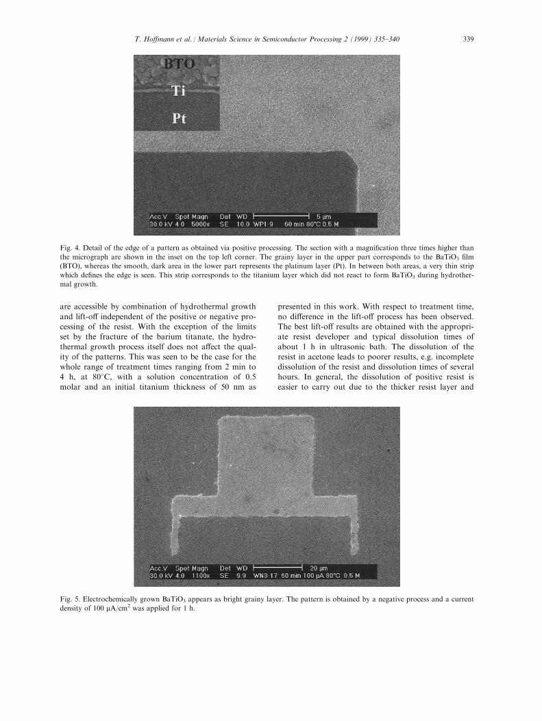
are comparable in size and shape to those observedbefore the hydrothermal treatment. Fig. 4 depicts a
section of an edge as obtained by the positive processin more detail. Dissolution of the resist leads to abreak of the barium titanate layer along the border of
the resist. Those parts of the barium titanate which aresupported by the resist are removed whereas the partsin direct contact with the substrate remain as micro-
structures. Closer inspection of the micrograph revealsthree di�erent areas: (i) a bright, grainy layer which
corresponds to barium titanate formed during the hy-drothermal treatment, (ii) a darker layer which corre-sponds to the platinum layer and (iii) a very thin strip
at the border of the grainy layer. The latter corre-sponds most likely to titanium which has not reactedwith the solution in the formation of the barium tita-
nate. The existence of such a titanium layer was ident-i®ed by X-ray di�raction. However, the fracture of the
barium titanate ®lm seems to run parallel to that ofthe titanium layer (Fig. 4).This result allows an estimation of the resolution
limit by the width of the titanium stripe which is ap-proximately 80 nm, a value su�cient to allow a fairlygood de®nition of micrometer features. It also may be
concluded that the fracture of the barium titanate doesnot occur necessarily along grain boundaries. Grains
have sizes between 100 and 200 nm and are randomlyarranged on the surface. A fracture along grain bound-aries would not follow a straight line but result in a
more tortuous border of the barium titanate thanthose seen in Fig. 4.
The minimum feature size in this work was 2.5 mmwhich corresponds to the separation of structures(Fig. 3b) or to the line width (Fig. 3d). It was limited
by the lithography technique used. Furthermore,enclosed structures like the ones shown in Fig. 3a and c
Fig. 3. Micrographs of patterns after hydrothermal growth
(60±120 min) and lift-o� are shown. The BaTiO3 ®lm (BTO)
appears brighter and the dark areas correspond to the under-
lying platinum layer (Pt). Patterns obtained by positive pro-
cessing of the resist are depicted in (a) and (b). Results of the
negative process are shown in (c) and (d). The resolution limit
of 2.5 mm is given either as the separation of structures (b) or
as the line width (d).
T. Ho�mann et al. / Materials Science in Semiconductor Processing 2 (1999) 335±340338
are accessible by combination of hydrothermal growth
and lift-o� independent of the positive or negative pro-
cessing of the resist. With the exception of the limits
set by the fracture of the barium titanate, the hydro-
thermal growth process itself does not a�ect the qual-
ity of the patterns. This was seen to be the case for the
whole range of treatment times ranging from 2 min to
4 h, at 808C, with a solution concentration of 0.5
molar and an initial titanium thickness of 50 nm as
presented in this work. With respect to treatment time,
no di�erence in the lift-o� process has been observed.
The best lift-o� results are obtained with the appropri-
ate resist developer and typical dissolution times of
about 1 h in ultrasonic bath. The dissolution of the
resist in acetone leads to poorer results, e.g. incomplete
dissolution of the resist and dissolution times of several
hours. In general, the dissolution of positive resist is
easier to carry out due to the thicker resist layer and
Fig. 4. Detail of the edge of a pattern as obtained via positive processing. The section with a magni®cation three times higher than
the micrograph are shown in the inset on the top left corner. The grainy layer in the upper part corresponds to the BaTiO3 ®lm
(BTO), whereas the smooth, dark area in the lower part represents the platinum layer (Pt). In between both areas, a very thin strip
which de®nes the edge is seen. This strip corresponds to the titanium layer which did not react to form BaTiO3 during hydrother-
mal growth.
Fig. 5. Electrochemically grown BaTiO3 appears as bright grainy layer. The pattern is obtained by a negative process and a current
density of 100 mA/cm2 was applied for 1 h.
T. Ho�mann et al. / Materials Science in Semiconductor Processing 2 (1999) 335±340 339

better edge de®nition. The use of ultrasonic bath doesnot appear to in¯ict any structural damage to barium
titanate ®lms, such as peel-o�.Galvanostatic experiments have been carried out in
order to test if the resist will withstand a combined hy-
drothermal±electrochemical treatment. Low currentdensities from 100 mA/cm2 to 10 mA/cm2 have beenapplied for 1 h. It was shown that the lift-o� technique
is also applicable after hydrothermal±electrochemicaltreatment (Fig. 5). In the range of the conducted ex-periments the resist withstood the treatment, although
the faster removal of the resist compared to the purelyhydrothermal treatment may indicate some chemicalreaction taking place during treatment. Typical dissol-ution times in the developer were in the range of 10 to
20 min and even in the case of acetone used as a sol-vent, lift-o� were possible within 30 min.
4. Conclusions
We have shown that the combination of hydrother-
mal growth at low temperatures and lift-o� allows thepatterning of BaTiO3 thin ®lms with minimum featuresizes of 2.5 mm. This limit is set by the lithography
technique used in the present work. The de®nition ofthe pattern edges is limited by two processes: (i) thecorrugation of the resist layer as observed after sput-tering of the titanium layer and (ii) by the fracture of
the BaTiO3 ®lm during lift-o�. Our results indicatethat the former limit may be overcome by a thickerresist layer. Additionally, an improvement of the sput-
ter process may be achieved by cooling of the sampleand lower plasma power. The limit set by the latterprocess is less than 100 nm and will allow patterning
in the range of mm. To achieve patterns with lateralsizes in the sub-micron range it is necessary to under-stand how the fracture of the thin BaTiO3 ®lm pro-ceeds during lift-o�. If grain sizes set a limit to the
resolution, than a convenient way to overcome thislimit would be the application of electrochemistrybecause of the control of nucleation and growth [17].
Therefore, our ®nding that electrochemistry and lift-o�are compatible is of particular importance for furtherdevelopment.
Acknowledgements
This work was supported by grants Fundacio n
Andes C-10810-2, C-12776 and C-12510 and FONDE-CYT 1930310. The authors wish to acknowledge Mrs.Judit G. Lisoni, Universidad de Chile, for her help in
XRD and Solvay Bario e Derivati, Italy for providingus with high purity Ba(OH)2 powder.
References
[1] Scott JF, Ross FM, Paz de Araujo CA, Scott MC,
Hu�man M. MRS Bulletin 1996;21(7):33.
[2] Auciello O, Scott JF, Ramesh R. Physics Today
1998;51(7):22.
[3] Kingon AI, Strei�er SK, Basceri C, Summerfelt SR.
MRS Bulletin 1996;21(7):46.
[4] Fork DK, Armani-Leplingrad F, Kingston JJ. MRS
Bulletin 1996;21(7):53.
[5] Polla DL, Francis LF. MRS Bulletin 1996;21(7):59.
[6] Yoshimura M, Yoo SE, Hayashi M, Ishizawa N. Jpn J
Appl Phys 1989;28(11):L2007.
[7] Bacsa RR, Rutsch G, Dougherty JP. J Mater Res
1996;11(1):194.
[8] Venigalla S, Bendale P, Adair JH. J Electrochem Soc
1995;142(6):2101.
[9] Ishizawa N, Banno H, Hayashi M, Yoo S, Yoshimura
M. Jpn J Appl Phys 1990;29(11):2467.
[10] Pilleux ME, Fuenzalida VM. J Appl Phys
1993;74(7):4664.
[11] Bacsa R, Dougherty JP, Pilione LJ. Appl Phys Lett
1993;63(8):1053.
[12] Shi E, Cho CR, Jang MS, Jeong SY, Kim H. J Mater
Res 1994;9(11):2914.
[13] Cho CR, Shi E, Jang MS, Jeong SY, Kim SC. Jpn J
Appl Phys 1994;33:4984.
[14] Xu W, Zheng L, Lin C, Okuyama M. J Electrochem Soc
1996;143(3):1133.
[15] Ho�mann T, Doll Th, Fuenzalida VM. J Electrochem
Soc 1997;144:L292.
[16] Ho�mann T, Fuenzalida VM. Mat Res Soc Symp Proc
1998;485:451.
[17] Escobar I, Silva C, Lorca L, Fuenzalida VM, Lisoni JG,
Vargas T. Mat Res Soc Symp Proc 1996;403:101.
T. Ho�mann et al. / Materials Science in Semiconductor Processing 2 (1999) 335±340340