microstructures of batio based ptc thermistors with ca,...
TRANSCRIPT
1
Microstructures of BaTiO3 based PTC thermistors with Ca,
Sr and Pb additions
L. Affleck, C. Leach*
Manchester Materials Science CentreUniversity of Manchester and UMIST
Grosvenor Street, Manchester M1 7HS, UK
Abstract
BaTiO3 based PTC thermistors undergo a large and rapid increase in resistance just above the
Curie temperature, TC. The resistance increase is predominantly associated with an increase in
grain boundary barrier height, therefore it is important to gain information about the grain
boundary character in these devices. In this study the microstructures of three different
BaTiO3 PTC thermistor formulations were compared by transmission electron microscopy.
The samples differed in the A-site substitutions, giving the formulae: (1) BaTiO3, (2)
(Ba,Ca)TiO3, (3) (Ba,Ca,Sr,Pb)TiO3. No grain boundary films were observed, though
rounding of the grains at the grain junctions was evidence of a liquid second phase being
present during sintering. EDX measurements were made across grain boundaries but no
significant segregation of elements to the boundaries was observed.
Keywords: Electron microscopy, Grain boundaries, Microstructure – final, PTC devices,
BaTiO3 and titanates.
* Corresponding author. Email address: [email protected]
2
1. Introduction
PTC thermistors such as donor-doped BaTiO3 undergo a large and rapid increase in resistance
just above the Curie temperature, TC. A-site substitutions of Sr or Pb are commonly added to
control the switching temperature TC.1 Ca may also be added for a grain-refining effect.2
The PTC effect is attributed to an increase in the potential barrier height at the grain
boundaries. The potential barrier has been attributed to the effects, both of a 2D layer of
acceptor states and a thin insulating layer at the grain boundary.3 The model of a 2D layer of
acceptor states at the grain boundary does not need a second phase film to be present. The
model of a thin insulating layer at the grain boundary was developed because some
experimental current-voltage data did not fit with the idea of a 2D layer of acceptor states.3
The thin insulating layer model requires the presence of a second phase film at the grain
boundaries.
Grain boundary films are common in ceramics, particularly at high angle grain boundaries,
since wetting can lower the grain boundary energy. Grain boundary films or intergranular
layers of a second phase have been predicted by some authors to give a better fit to the
measured current-voltage data than is possible without such a layer.4,5 Gerthsen and
Hoffmann4 proposed a 600 nm thick layer of TiO2-rich second phase at the grain boundaries
of BaTiO3, while Hayashi et al5 proposed a 100 nm thick layer of BaTiO3 with acceptor point
defects at the grain boundaries. However, most studies of the microstructure of barium
titanate by transmission electron microscopy (TEM), to a resolution of 2-10 nm, did not show
the presence of any grain boundary films or intergranular layers of a second phase.6,7 There
has been only one reported TEM observation of such a layer at the grain boundaries.8
3
Evidence for the 2D layer of acceptor states model would include segregation of acceptor
atoms to the grain boundaries. Segregation of elements such as Fe to the grain boundaries has
been observed by STEM in conjunction with energy-dispersive X-ray analysis (EDAX).7
In this study the microstructures of grain boundaries in thermistor formulations with differing
compositions are compared, using TEM and SEM, to characterise the influence of A-site
substitutions on grain boundary character.
2. Experimental
Commercial donor-doped BaTiO3 pellets were supplied by GE Thermometrics (UK) Ltd in
three different formulations based on BaTiO3, (Ba,Ca)TiO3 and (Ba,Ca,Sr,Pb)TiO3. The
pellets were prepared by sintering at a peak temperature of 1300°C.
Thin specimens were prepared for analysis by TEM, by grinding, cutting and mounting onto a
Cu grid, followed by dimpling and ion beam thinning. A Philips CM200 TEM, fitted with an
EDAX energy-dispersive X-ray spectrometer, was used to analyse the microstructure and
composition of the specimens. A FEI Tecnai F30 FEGTEM/STEM fitted with an EDAX
spectrometer was used to obtain compositional linescan information across a grain boundary.
Thermistor pellets were also polished with colloidal silica in order to obtain orientation
contrast in backscattered electron images, using a Philips XL30 FEGSEM.
4
3. Results and Discussion
3.1. Second phases
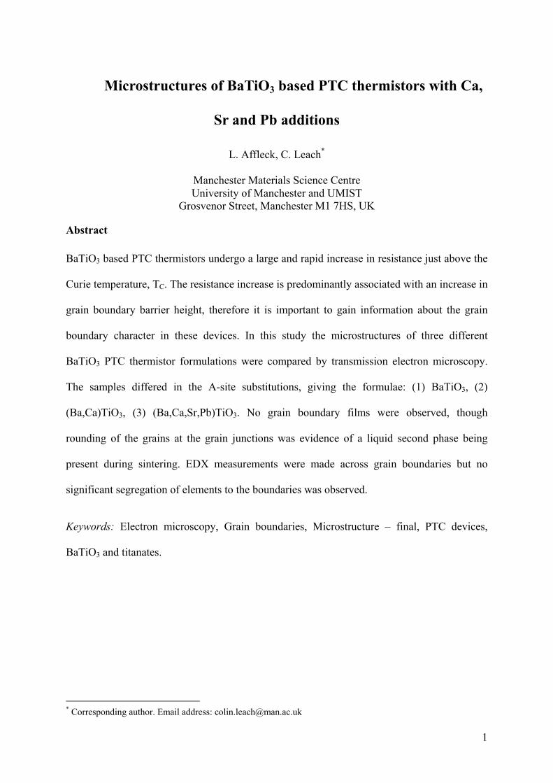
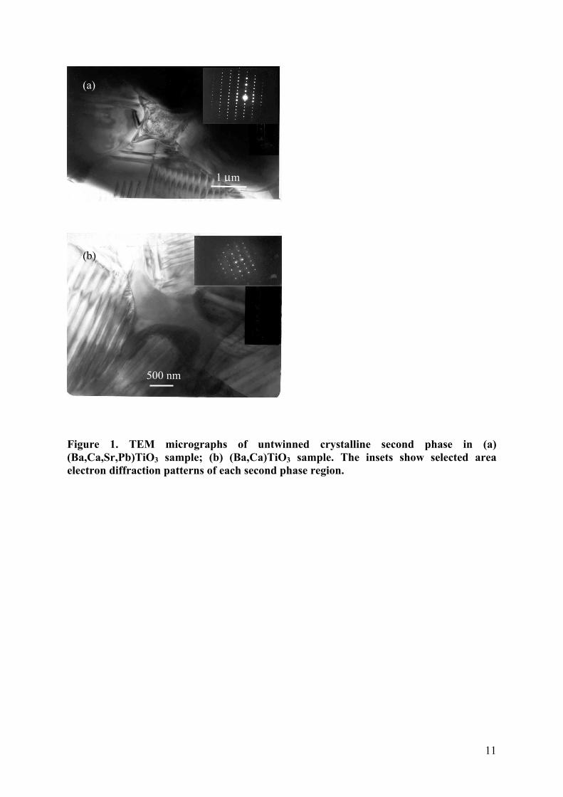
A crystalline, untwinned second phase was seen in all the samples (Figure 1). It was located at
triple junctions, and varied in width from a few nm to 2 µm. The second phase contained Ba,
Ti, O and reduced levels of dopants. It was silicon-rich (~16%) in all samples, except for the
(Ba,Ca)TiO3 formulation where it was just composed of Ba, Ti and O. In this sample, Ca was
only detected within the grains and Si was not detected at all.
The angle that the second phase makes with the grains can provide information about wetting
behaviour. For a grain boundary to be wet by a second phase, the dihedral angle, Φ, must be
less than 60°. TEM micrographs of the second phases at grain junctions in the samples studied
here show a range of dihedral angles, mainly from ~30° to 50°, although a few larger angles
were noted. This suggests that in most cases grain boundary wetting should occur, i.e. a layer
of second phase should be seen at the interface between two grains.
3.2. Grain boundary films
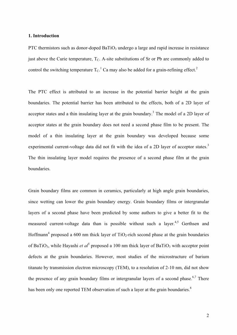
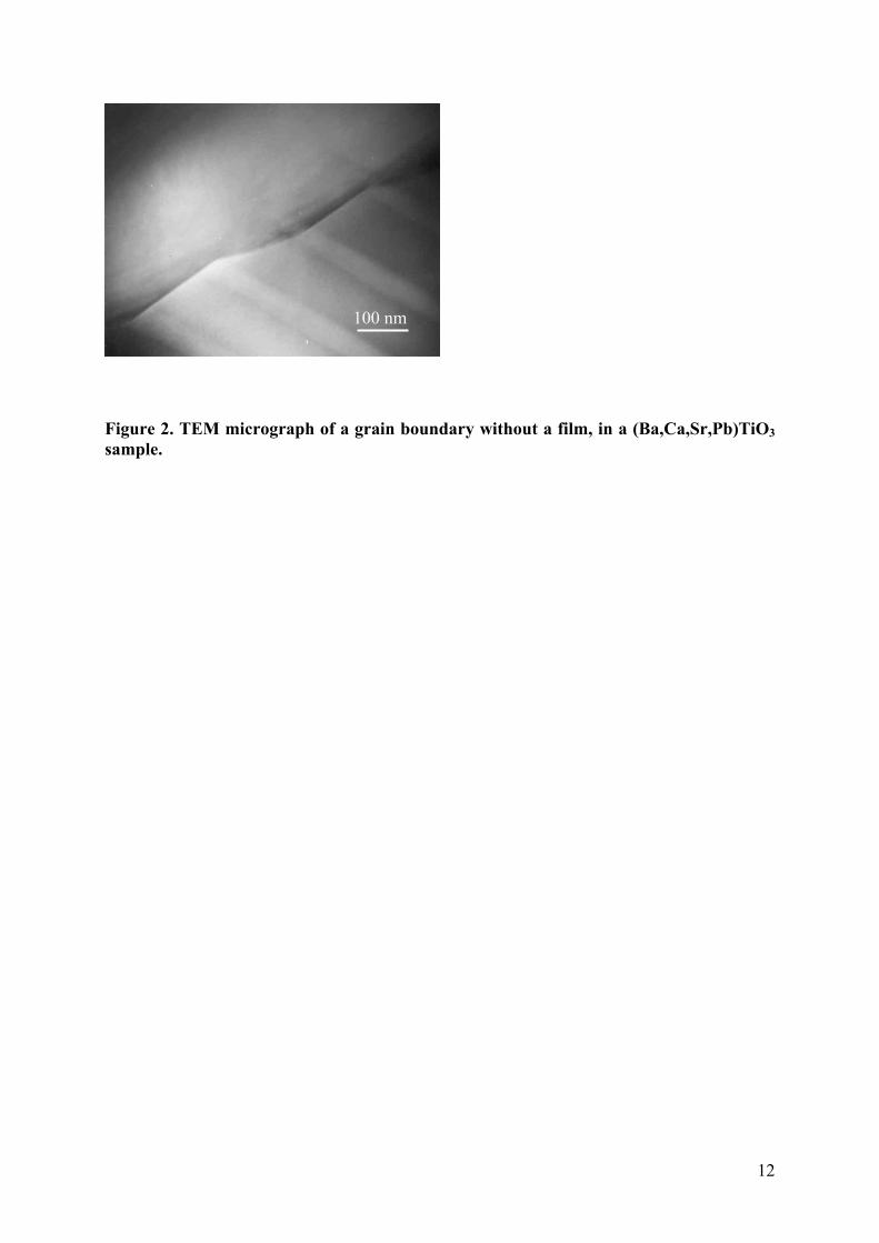
No grain boundary films thicker than 50 nm were observed in any of the samples (Figure 2).
Some rounding of grains at the grain junctions was observed, however, which was evidence
of a liquid grain boundary phase being present during sintering (Figure 1). It is possible that
some grain boundaries were wetted at high temperatures during sintering, but de-wetted upon
cooling. Previous studies on the role of sintering aids in BaTiO3 thermistors have inferred the
presence of a liquid phase around the grains at the sintering temperature, but that this
accumulates at grain junctions upon cooling leaving boundaries virtually free of second
phase.9

5
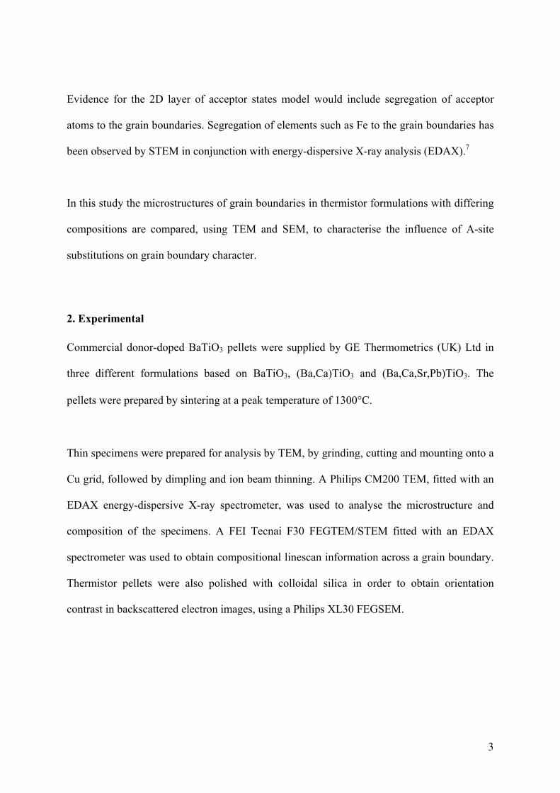
3.3. Segregation
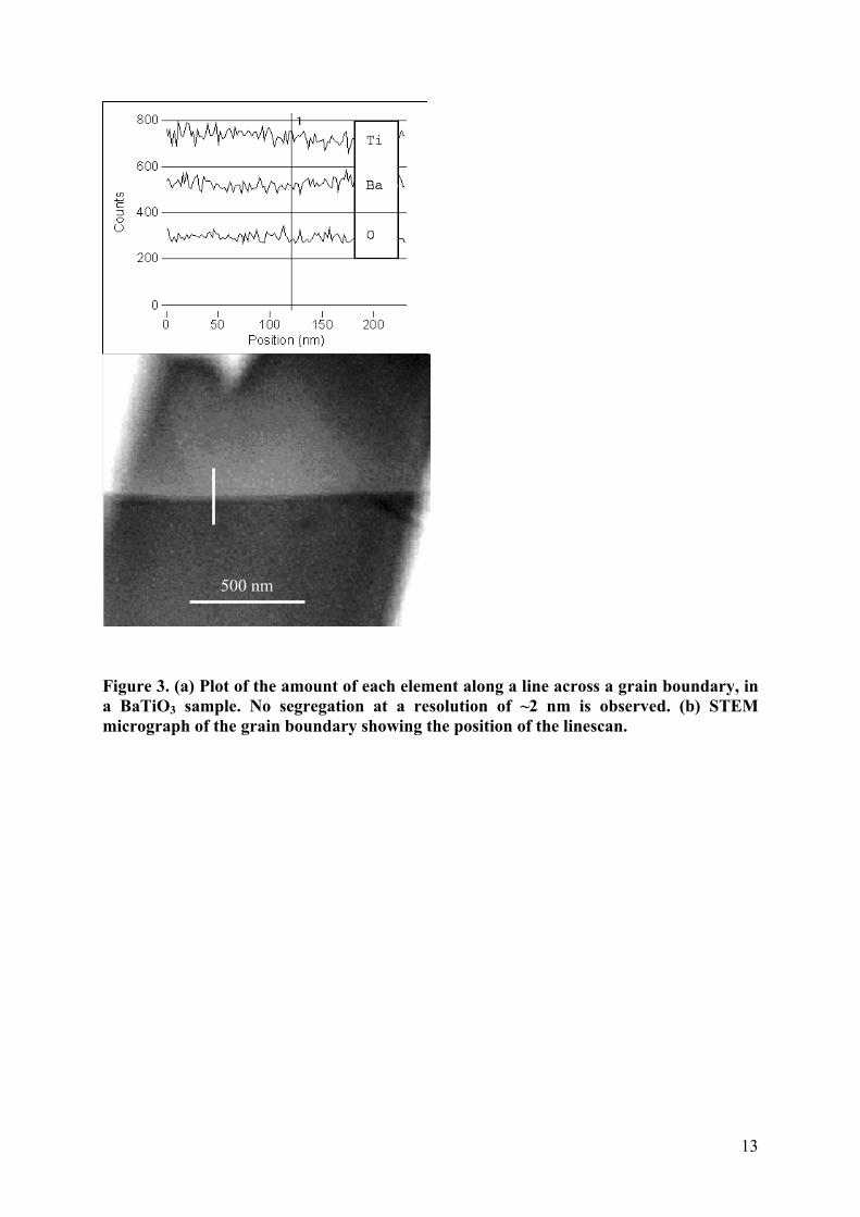
A series of spot EDX analyses was made across a grain boundary in each sample, to
determine whether any segregation of elements to the boundary could be detected. The
nanoprobe TEM mode was used; the electron spot width for analysis was about 15 nm. A
suitable grain boundary, that was parallel to the electron beam during analysis, was found in
each sample. Spot analyses taken at the grain boundary interface and to either side showed no
evidence for grain boundary segregation. Additionally a linescan across a grain boundary in a
BaTiO3 sample was performed, with analyses taken every 2 nm using a 2 nm spot size
(Figure 3). The line in Figure 3(a) shows the position of the grain boundary. Again, no
evidence for grain boundary segregation was observed. It was concluded that, in the samples
studied here, any segregation of elements to the grain boundary was below the detectability
limit of the EDAX detector (~0.5 %).
3.4. Twins
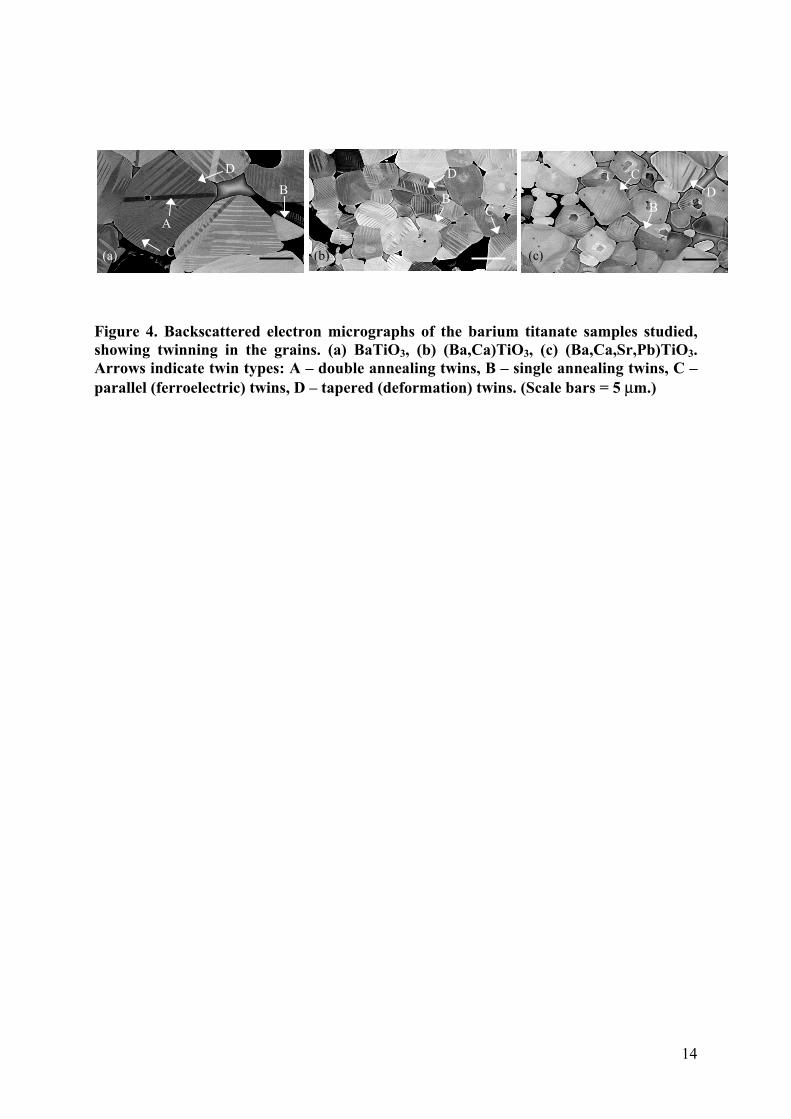
The microstructures of each barium titanate formulation show twinning in most grains (Figure
4). The width of the twin domains and the spacing between them was measured from TEM
micrographs, with the twin planes oriented parallel to the electron beam. Generally the twins
are between a few 10s and a few 100s of nanometres wide.
Figure 4(a) shows the twinning in the BaTiO3 sample, in which many grains contained a
double annealing twin (A), running across the grain. Such twins were not observed in the
(Ba,Ca)TiO3 and (Ba,Ca,Sr,Pb)TiO3 samples, Figure 4(b) and (c). All of the samples had
single annealing twins (B), straight parallel (ferroelectric) twins (C) and tapered (deformation)
twins (D). The ferroelectric twin planes in each sample were indexed and found to be {101},
in common with other published data.10 In BaTiO3, {101} twins form during the cubic to
6
tetragonal phase transformation, to release the induced stresses.11 {111} annealing twins form
during sintering and are associated with abnormal grain growth.11
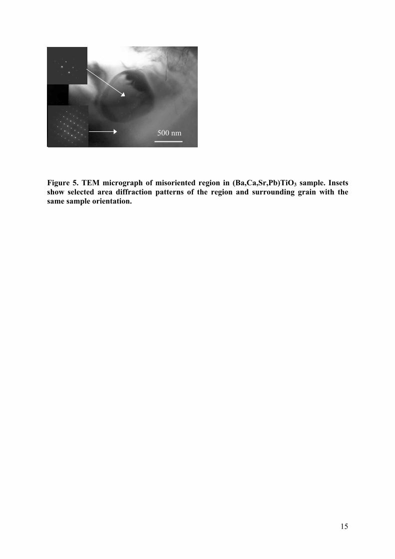
3.5. Misoriented regions
In the (Ba,Ca,Sr,Pb)TiO3 sample, some grains contained small regions of about 1 µm
diameter that were of a similar composition but slightly misoriented with respect to the
surrounding grain. Figure 5 shows a TEM bright field image of such a misoriented,
untwinned, region along with diffraction patterns from this region and the surrounding grain.
The misorientation is described by a rotation of 5.1° in the plane of the sample and a 7.5°
about an axis parallel to the electron beam. The interface with the host grain is sharp. The
origin of these regions is currently uncertain and will be the subject of further study.
4. Conclusions
The microstructures of three different compositions of PTC thermistors based on BaTiO3 with
different A-site substitutions were compared by TEM and were found to be similar in many
respects. No grain boundary film and no evidence for segregation of elements to the grain
boundaries were observed in any of the samples. In the BaTiO3 and (Ba,Ca,Sr,Pb)TiO3
samples a crystalline Si-rich second phase was found at the junctions of rounded grains,
implying that the second phase was liquid at the sintering temperature. All the samples had a
spread of twin widths between a few 10s and a few 100s of nanometres wide. Ferroelectric,
deformation and single annealing twins were observed in all samples. The BaTiO3 sample
also had double annealing twins. The (Ba,Ca,Sr,Pb)TiO3 sample contained some misoriented
regions that were not observed in the other compositions.

7
Acknowledgements
This work was funded through EPSRC grant number GR/R00500/01. GE Thermometrics
(UK) Ltd are thanked for the supply of the thermistor pellets used in this study. Peter Kenway
of the Manchester Materials Science Centre is thanked for his help with the TEM studies.
8
References
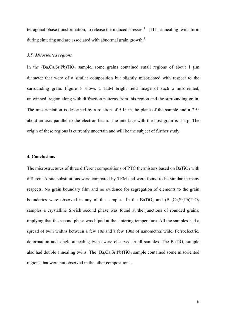
1. Hill, D. and Tuller, H., Ceramic Sensors: Theory and Practise. In Ceramic Materials
for Electronics, (Ed. R. Buchanan), Marcel Dekker Inc, NY, 1991, p335.
2. Voltzke, D., Abicht, H., Pippel, E. and Woltersdorf, J., Ca-containing additives in
PTC-BaTiO3 ceramics: effects on the microstructural evolution. J. Eur. Ceram. Soc.,
2000, 20, 1663-1669.
3. Daniels, J. and Wernicke, R., New aspects of an improved PTC model. Philips Res.
Repts., 1976, 31, 544-559.
4. Gerthsen, P. and Hoffmann, B., Current-voltage characteristics and capacitance of
singe grain boundaries in semiconducting BaTiO3 ceramics. Solid State Electronics,
1973, 16, 617-622.
5. Hayashi, K., Yamamoto, T., Ikuhara, Y. and Sakuma, T., Grain boundary electrical
barriers in positive temperature coefficient thermistors. J. Appl. Phys., 1999, 86, 2909-
2913.
6. Hayashi, K., Yamamoto, T., Ikuhara, Y. and Sakuma, T., Formation of potential
barrier related to grain-boundary character in semiconducting barium titanate. J. Am.
Ceram. Soc., 2000, 83, 2684-2688.
7. Desu, S. and Payne, D., Interfacial Segregation in Perovskites: 2, Experimental
Evidence. J. Am. Ceram. Soc., 1990, 73, 3398-3406.
8. Rehme, H., Imaging electric microfields in emission electron microscope. Z. angew.
Physik, 1970, 29, 173.
9. Cheng, H., Effect of sintering aids on the electrical properties of positive temperature
coefficient of resistivity BaTiO3 ceramics. J. Appl. Phys., 1989, 66, 1382-1387.
9
10. Hu, Y., Chan, H., Wen, Z. and Harmer, M., Scanning Electron Microscopy and
Transmission Electron Microscopy Study of Ferroelectric Domains in Doped BaTiO3.
J. Am. Ceram. Soc., 1986, 69, 594-602.
11. Lee, B. and Kang, S., Second-phase assisted formation of {111} twins in barium
titanate. Acta Mater., 2001, 49, 1373-1381.
10
List of figures
Figure 1. TEM micrographs of untwinned crystalline second phase in (a)(Ba,Ca,Sr,Pb)TiO3 sample; (b) (Ba,Ca)TiO3 sample. The insets show selected areaelectron diffraction patterns of each second phase region.
Figure 2. TEM micrograph of a grain boundary without a film, in a (Ba,Ca,Sr,Pb)TiO3sample.
Figure 3. (a) Plot of the amount of each element along a line across a grain boundary, ina BaTiO3 sample. No segregation at a resolution of ~2 nm is observed. (b) STEMmicrograph of the grain boundary showing the position of the linescan.
Figure 4. Backscattered electron micrographs of the barium titanate samples studied,showing twinning in the grains. (a) BaTiO3, (b) (Ba,Ca)TiO3, (c) (Ba,Ca,Sr,Pb)TiO3.Arrows indicate twin types: A – double annealing twins, B – single annealing twins, C –parallel (ferroelectric) twins, D – tapered (deformation) twins. (Scale bars = 5 µm.)
Figure 5. TEM micrograph of misoriented region in (Ba,Ca,Sr,Pb)TiO3 sample. Insetsshow selected area diffraction patterns of the region and surrounding grain with thesame sample orientation.
11
Figure 1. TEM micrographs of untwinned crystalline second phase in (a)(Ba,Ca,Sr,Pb)TiO3 sample; (b) (Ba,Ca)TiO3 sample. The insets show selected areaelectron diffraction patterns of each second phase region.
1 µm
(a)
500 nm
(b)
12
Figure 2. TEM micrograph of a grain boundary without a film, in a (Ba,Ca,Sr,Pb)TiO3sample.
100 nm
13
Figure 3. (a) Plot of the amount of each element along a line across a grain boundary, ina BaTiO3 sample. No segregation at a resolution of ~2 nm is observed. (b) STEMmicrograph of the grain boundary showing the position of the linescan.
500 nm
14
Figure 4. Backscattered electron micrographs of the barium titanate samples studied,showing twinning in the grains. (a) BaTiO3, (b) (Ba,Ca)TiO3, (c) (Ba,Ca,Sr,Pb)TiO3.Arrows indicate twin types: A – double annealing twins, B – single annealing twins, C –parallel (ferroelectric) twins, D – tapered (deformation) twins. (Scale bars = 5 µm.)
(b)
B
CD
(a) (c)
A
C
BD
BC
D
15
Figure 5. TEM micrograph of misoriented region in (Ba,Ca,Sr,Pb)TiO3 sample. Insetsshow selected area diffraction patterns of the region and surrounding grain with thesame sample orientation.
500 nm