misfet-based biosensing interface for neurons guided
TRANSCRIPT
HAL Id: hal-01504965https://hal.archives-ouvertes.fr/hal-01504965
Submitted on 10 Apr 2017
HAL is a multi-disciplinary open accessarchive for the deposit and dissemination of sci-entific research documents, whether they are pub-lished or not. The documents may come fromteaching and research institutions in France orabroad, or from public or private research centers.
L’archive ouverte pluridisciplinaire HAL, estdestinée au dépôt et à la diffusion de documentsscientifiques de niveau recherche, publiés ou non,émanant des établissements d’enseignement et derecherche français ou étrangers, des laboratoirespublics ou privés.
MISFET-based biosensing interface for neurons guidedgrowth and neuronal electrical activities recording
Florian Larramendy, Amel Bendali, Marie-Charline Blatché, Fabrice Mathieu,Serge Picaud, Pierre Temple-Boyer, Liviu Nicu
To cite this version:Florian Larramendy, Amel Bendali, Marie-Charline Blatché, Fabrice Mathieu, Serge Picaud, et al..MISFET-based biosensing interface for neurons guided growth and neuronal electrical activities record-ing. Sensors and Actuators B: Chemical, Elsevier, 2014, 203, pp.375 - 381. �10.1016/j.snb.2014.06.106�.�hal-01504965�

1
MISFET-based biosensing interface for neurons guided growth and
neuronal electrical activities recording
F. Larramendy1,2, A. Bendali3,4,5, M.C. Blatché1,2, F. Mathieu1,2,
S. Picaud3,4,5,6, P. Temple-Boyer1,2, L. Nicu1,2
1 CNRS, LAAS, 7 avenue du colonel Roche, F-31400 Toulouse, France
2 University of Toulouse, UPS, LAAS, F-31400 Toulouse, France
3 INSERM, U968, Institut de la Vision, Paris, 75012, France
4 UPMC, University of Paris 06, UMRS968, Institut de la Vision, Paris, 75012, France
5 CNRS, UMR7210, Institut de la Vision, Paris, 75012, France
6 Fondation Ophtalmologique Adolphe de Rothschild, Paris, 75019, France
Abstract
A hybrid circuit of a transistor-based chip was implemented and characterized for the
neuronal electrical activity recording. The integration of microfluidic architectures was developed
to control precisely neurites outgrowth and form topologically defined and stable neural networks.
Individual neural cells from rat retinae and Lymnaea stagnalis snails were immobilized on gates
regions of Metal Insulator Semiconductor Field Effect Transistors (MISFET). Neuronal orientation
was achieved in both cases but neuronal action potentials were only recorded in the Lymnaea
stagnalis case. They were successfully triggered and inhibited by implementing a picrotoxin -
GABA – picrotoxin injection protocol, exhibiting a direct influence of picrotoxin on the "spike
type" action potential waveform. The implementation of the whole process of neuronal culture and
subsequent activity monitoring constitutes a proof-of-principle experiment for the development of
neuroelectronic systems for signal processing studies adapted to low-density neuronal cultures.
Keywords: FET microdevice, neuronal interface, action potential measurement
2
1. Introduction
The study of the neuronal network dynamics in brain tissue is a difficult task owing to the large
number of closely packed neurons with complex synaptic connectivity and the difficulty of
monitoring activity in the neural network at the single-cell resolution with non-invasive techniques.
In principle, low-density cultures of nerve cells drastically reduce the network complexity but
uncertainty on the synaptic wiring remains. Furthermore, while single cell recording can be easily
obtained by patch clamp recording [1], it is very challenging to achieve multicellular recordings
with this approach. By contrast, the use of cell non-invasive extracellular multi-electrode array
(MEA) enabled recordings and stimulations of large cell numbers [2,3]. Similarly, planar MEA
were used for neurons culture for days and months without inflicting mechanical damage to the
neuronal membrane [4]. This involves electrical measurements (voltage or current) across the cell
membrane [5]. Nevertheless, such extracellular electrical interfacing of neurons was implemented
with planar metal electrodes on insulating substrates [6-8], associated with organic transistors [9] or
integrated with semiconductor devices using Complementary Metal Oxide Semiconductor (CMOS)
technology [10,11]. In all cases, the activity of a nerve cell – i.e. the action potential – is stimulated
and/or recorded by interfacing individual nerve cells with electrical microdevices that locally
generate and/or sense electrical field variations towards medical applications [12]. So far, efforts
have been focused onto interfacing nerve cells in order to measure and interpret the neuronal action
potential and greater sensitivity would be required to measure smaller cell signals. One of the first
way to “communicate” with nerve cells or to make them inter-communicate using microelectrodes
was achieved by Jerome Pine [13] and Guenter Gross [14]. Then, Peter Fromherz proposed to use
MOS technology in order to integrate microelectrode arrays [15], emphasizing the following
principle: (i) neuronal activity is elicited by capacitive stimulation from a silicon chip and (ii)
neuronal activity is recorded by a transistor located on the same chip. Nevertheless, the signal-to-
noise ratios were relatively small often preventing the distinction between single cell recordings and
multi-unit activity. Inspired by Fromherz’s seminal works [16,17], Charles Lieber’s team
demonstrated enhanced signal-to-noise ratios using arrays of nanowire field-effect transistors
connected to individual axons or dendrites of mammalian neurons [18]. In this report, each
nanoscale junction was used for spatially resolving stimulations, and/or inhibitions of propagating
neuronal signals with great detection sensitivity.
Moreover, neural patterning has attracted much interest in neural electronics [19] and neural
engineering [20]. Compared with randomly cultured neurons, patterned neurons possess a much
simpler network structure, which is easier for network modelling and signal analysis. In addition,
the amplitude of detected action potentials of neurons is higher when neurons are located directly

3
on the electrodes [6]. With these advantages, different protocols have been developed to perform
and optimize neuron positioning and neurite growth. Thus, methods such as micro-contact printing
[19], photodegradation [21], microfluidic structuration [22], biomolecule patterning [23] and
photoresist processing [24] were applied for constraining neurons and guiding neurites on planar
substrates.
In the present study, we have produced neural networks with defined topology on a substrate
with appropriate integrated electrical contacts for each (or groups of) neuron(s). This bottom-up
approach faced three objectives: i) non-invasive electrical interfacing of individual neuronal cell
bodies, ii) control of neurites outgrowth to form topologically defined and stable networks, and iii)
the integration of both defined networks and extracellular interfacing in a same, dedicated system.
Our transistor-based biosensing interface solved these three challenges at once.
2. Materials and Methods
2.1. Design and fabrication of biosensors
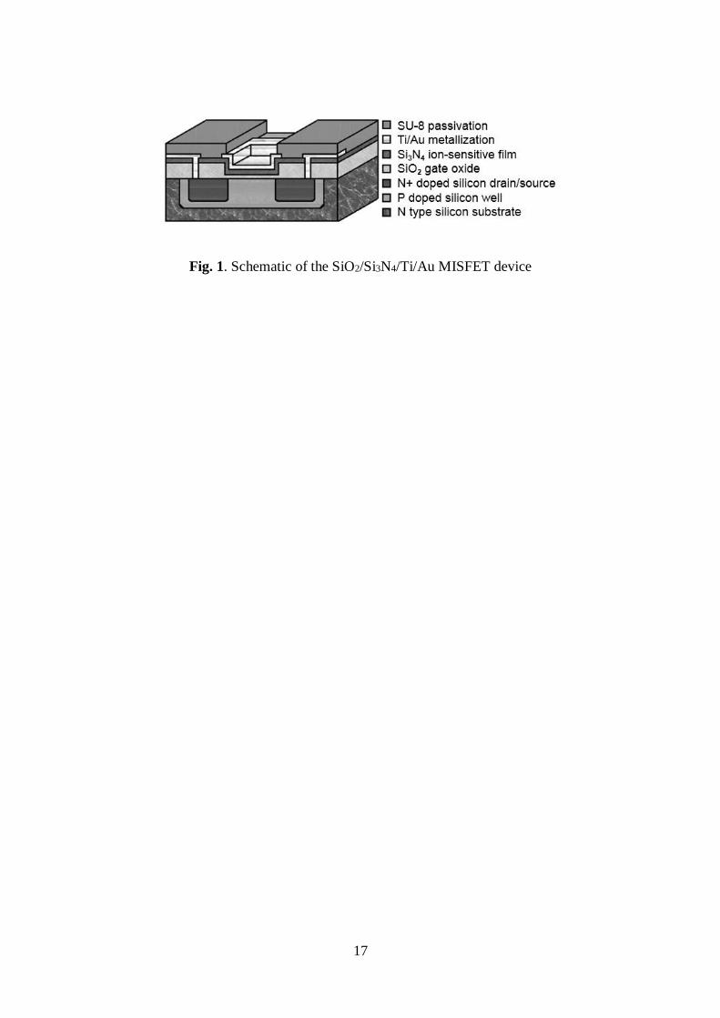
Considering a SiO2/Si3N4 pH-sensitive chemical field effect transistor (pH-ChemFET)
technology [25], N-channel metal-insulator-semiconductor field effect transistors (MISFET) were
realized. The MISFET fabrication and encapsulation processes were previously described [26] but
briefly reminded hereafter. Starting with a 6 inch, N-type (1×1013 cm-²), (100) silicon wafer, P-
doped wells were realized by boron implantation (1×1015 cm-²) and, following, N-doped source and
drain regions were formed by arsenic implantation (1×1018 cm-²). The gate was then fabricated
through the stacking of thermal silicon oxide SiO2 (50 nm-thick), LPCVD silicon nitride Si3N4 (50
nm-thick) and PVD titanium/gold thin films (600 nm-thick). The MISFET has a 10 µm-long and
200 µm-wide metallic gate. Wafer-level passivation was finally performed using a polymer-based
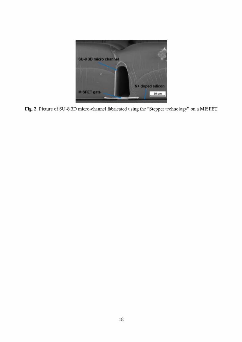
technology. Figure 1 shows a schematic of the SiO2/Si3N4/Ti/Au MISFET device. A 50 µm-thick
SU-8 photoresist layer was patterned to fabricate 10 µm-wide and 35 µm-high 3D microfluidic
channels as well as micro-tanks and neurons areas of reception using the “Stepper technology” [27].
Figure 2 shows a scanning electron microscope (SEM) cross-section revealed by Secco etching [28]
of a SU-8 3D micro-channel integrated on a MISFET transistor. In order to increase interactions
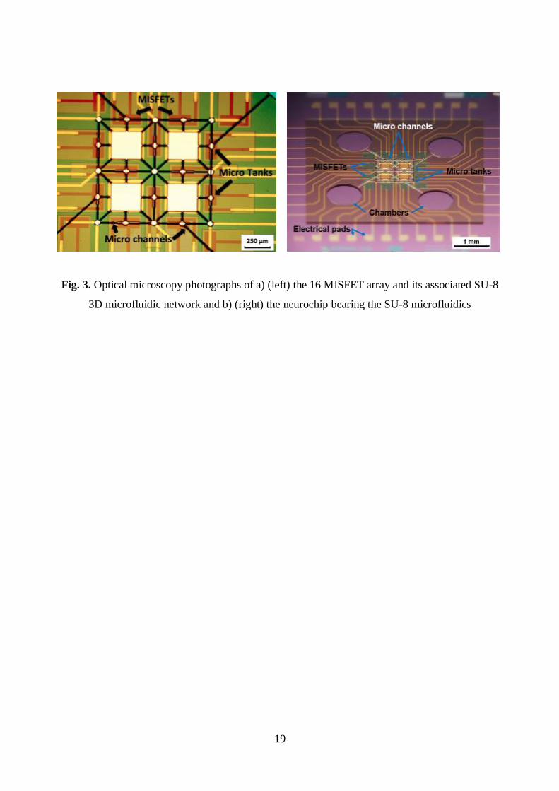
with the future neural networks, 16 MISFET devices were realized on a same chip in conjunction
with the upper SU-8 microfluidic channels (Figure 3 a). The final 16-MISFET array (1 mm2
surface) and its associated microfluidic network (Figure 3 b) are referred to as "neurochip"
hereafter. Finally, the neurochips were packaged on a printed circuit board (PCB) by flip-chip
4
bonding. Electronic contacts were isolated from the sensitive area thanks to an under-fill, and a
Pyrex ring was glued on the PCB to create a chamber for the cultured cells [26].
2.2. FET filter system for liquid phase measurements
An associated electronic card was specifically developed to interface the neurochips [26].
Thanks to this set-up, it is possible to multiplex the 16 MISFET on the neurochip while filtering any
noise coming from the electronic interface and/or the liquid. All devices were biased using the same
electrical configuration: a silver / silver chloride (Ag/AgCl) wire was used to apply the gate voltage
to the neuronal culture medium and the same drain source current and voltage (IDS = 250 µA and
VDS = 2 V). Thus, the different measurements related to neuronal action potentials were comparable
from one MISFET to the other. The resting potential was fixed to 0 V due to the removal of any
direct current (DC) component.
2.3. Rat retina neuronal cell culture
Cell cultures were prepared from Long-Evans rats, which were purchased from Janvier Company
(Le Genest Saint-Isle, France). All experiments were carried out in accordance with European
Community Council Directives (86/609/EEC) and with the ARVO (Association for Research in
Vision and Ophthalmology) statement for the use of animals in ophthalmic and visual research.
Ethics committee approval is not required for cell culture experiments, as stated in European Union
Directives (2010/63/UE). Animals were killed by CO2 sedation and cervical elongation, and all
efforts were made to minimize suffering.
Neuronal cells were isolated from the retina of newborn Long-Evans rats (postnatal day 7), with
an immunopanning technique, according to protocols previously described in young rats [29]. The
chips were coated with poly-D-lysine (2 µg/cm² for 45 min; Sigma-Aldrich) followed by laminin (1
µg/cm² overnight; Sigma-Aldrich). Cells were seeded in ND-G medium at an initial density of 4 x
104 cells/cm² on SU-8 microfluidic samples. The cultures were kept in an incubator at 37°C with
5% CO2 for three days. Then, after this three-day period, optical characterisations of neurons
growth were immediately performed at room temperature.
2.4. Lymnaea Stagnalis neuronal cells culture
Lymnaea Stagnalis (freshwater snails) were purchased from the National Institute of Agronomic
Researches (INRA) of Rennes (France), namely from the Experimental Unit of Aquatic Ecology

5
and Ecotoxicology section. Laboratory-raised stocks of Lymnaea Stagnalis were maintained in
aquaria filled with well-aerated filtered water at 22°C. Experiments were performed on 3-month-old
snails (20–30·millimeters in length). Snail neurons were chosen since, first, they exhibit high action
potentials (10-100 mV) and, second, their culture and electrophysiological characterization are
performed at room temperature, i.e. with no need for temperature control [30-34]. Thus, their
isolation followed previously established protocols [30-32]. Lymnaea Stagnalis were de-shelled,
soaked in 25% lysterin in normal saline consisting of 51.3 mM NaCl, 1.7 mM KCl, 4.1 mM CaCl2,
1.5 mM MgCl2 and 5.0 mM HEPES at pH 7.9 (all from Sigma-Aldrich) for 10 minutes. Central
ganglionic rings were isolated from Lymnaea in normal saline and put in 150 µg/mL gentamicin for
10 minutes at room temperature. Left and right pedal ganglia were isolated from the rest of the brain
and treated with 1.33 mg/mL collagenase and 0.67 mg/mL trypsin (all Sigma-Aldrich) for 30
minutes. Pedal ganglia were washed several times in Leibovitz L15 medium (Sigma-Aldrich).
Ganglia were dislocated using a micropipette in Leibovitz L15 medium while sucking, and the
contents were dispensed back into the same container. The operation was repeated until most tissues
were dispersed. Neuronal solution was divided up on different chips previously coated with poly-D-
lysine (2 µg/cm² for 45 minutes; Sigma-Aldrich) followed by laminin (1 µg/cm² overnight; Sigma-
Aldrich). The completed medium consisting of Leibovitz L15, 20 µg/mL gentamycin, 30 mM
glucose and 10 ng/mL nerve growth factor (NGF), was applied to different chambers (250
µL/chambers). The neurons were incubated for three days at room temperature (around 21°C).
Finally, all optical characterizations and electrical measurements with snails' pedal neurons were
performed at room temperature.
2.5. Cell viability assessment
Neuronal cells were visualized with the “lived-dead” test (Life Technologies) that consists in
labelling viable cells with calcein-AM being detected as green fluorescence, whereas dead cells
were labelled with ethidium iodide producing a red fluorescence. Briefly, after three days in culture,
chips bearing SU-8 3D microfluidics were incubated in a mixture of calcein-AM and ethidium
homodimer-1 (diluted in a phosphate buffer medium PBS, pH = 7.4) for one hour in a humidified
chamber (37°C, 5% CO2). Calcein-AM-positive viable cells were visualized under an
epifluorescence microscope (Leica DM 5000B, Solms, Germany). The silicon chips were mounted
with Fluorsave reagent (Calbiochem, San Diego, CA, USA) and viewed with an upright confocal
microscope (Nikon, Tokyo, Japan). The chips emitted a blue self-fluorescence (excitation at 408
nm) and the cells a green fluorescence (excitation at 488 nm).
6
2.6. Neuronal cell fixation for electron microscopy observations
After checking the viability of cells on each chip using epifluorescence microscopy, the culture
medium was removed. For fixation, the chips were rinsed with phosphate buffered saline (PBS) and
then incubated in 2.5% glutaraldehyde solution (Sigma-Aldrich) for 12 hours at 4°C. Then, the
glutaraldehyde solution was removed and chips were rinsed with PBS. For cell dehydration, we
used different ethanol solutions with increasing concentrations in water. The cells were therefore
incubated in 50%, 70%, 90% and 100% of ethanol for 10 minutes each. After the last dehydration
step, the fixated samples were air dried for a day to remove all alcoholic residues before observation
under a scanning electron microscope (SEM).
2.7. Toxin treatments for modulating action potentials activities
Electrical measurements of neuronal activities were only performed on Lymnaea Stagnalis pedal
neurons at room temperature as previously established in the literature [30-34].
For the action potential recordings, two different toxins were used to modulate neuronal activity.
The first was picrotoxin, which is known to excite silent cells [35]. We used 100 µM of picrotoxin
to trigger neuronal activity. Gamma-amynobutyric acid (GABA), an antagonist of picrotoxin, was
also tested in order to inhibit electrical firing of action potentials: 100 µM of GABA was necessary
to reverse picrotoxin-induced excitation. As a result, picrotoxin – GABA – picrotoxin sequential
injections were performed in order to reverse the action induced by the other, thus modulating
neuronal activity.
Finally, a cleaning procedure was developed for our MISFET chip. Medium with toxin was
removed thanks to a rinse cycle with deionised water. Then, the SU-8 microfluidic system was
filled with classic liquid hand soap, cleaned with a soft mechanical cleaning technique, and rinsed
finally with water. After undergoing the preliminary treatments as described before cells could
again be cultured and the neurochip could be reused. We were able to use the biosensor for more
than 15 cultures without degrading the SU-8 micro channels and/or the MISFET structures.
3. Results and discussion
3.1. Neuronal orientation
The first objective of our work was to generate on-chip guided growth of the neurons in order to
increase their contact with our MISFET sensors. We first evaluated if SU-8 micro-channels above
7
the transistors’ gates (Figure 3) could induce the neuronal guided growth. To overcome the well-
known SU-8 cytotoxicity [36], we proceeded to a four-step specific protocol necessary to turn the
SU-8 biocompatible. The first step is chemical treatments with SU-8 developer in order to remove
all resist residues thanks to SU-8 over-development. The second step is a photolithographic one that
allows to reflow the SU-8 resist across all its thickness thanks to a one minute UV exposure at a 365
nm wavelength. The third step is a thermal annealing at 150°C during three days to eliminate all
solvents still trapped inside the SU-8 layer. The final step is an O2 plasma treatment to render the
SU-8 surface hydrophilic [37]. SEM observations and measures before and after the specific
treatment have shown that this protocol do not affect the final dimension of SU-8 structures or
adhesion between the SU-8 layer and the substrate nor does it induce cracks in the SU-8 layer. After
performing the protocol, we deposited poly-D-lysine and coated using laminin in order to create a
favourable substrate that improves the efficiency of cell expansion and neuronal differentiation
[38].
Rat retina neurons were cultured on the neurochips previously coated with poly-D-lysine and
laminin. As mentioned previously (cf. 2.3), rat retina neurons were kept in a humidified chamber
(37°C, 5% CO2) for three days. Neuronal growth was assessed by microscopy and cell viability was
tested thanks to viability test described previously. An epifluorescence microscope (Leica DM4000
B LED) was used to visualize viable cells showing that more than 95% of cells survived on the chip
after three days of culture at 37°C. Rat retinal neurons limited their development to the reception
areas and towards the SU-8 micro channels. These first results demonstrate the guided neurites
growth towards the MISFET gate. Neurons were then examined at a smaller resolution to define if
they constitute a neuronal network on the neurochip. Confocal and fluorescence spectroscopies
were used to visualize neurons on the surface for two different microchannels configurations
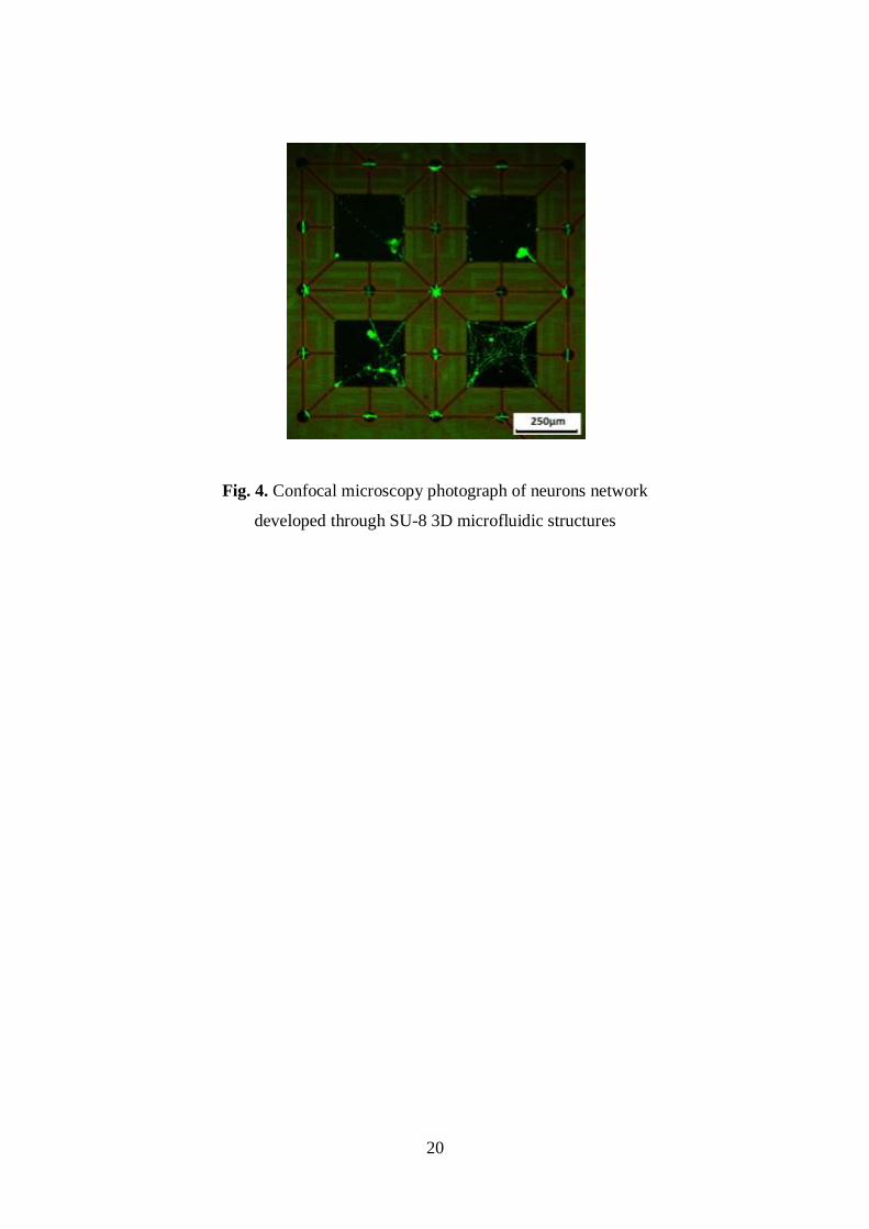
(Figures 4 and 5). Figures 4, 5 and 6 illustrate that many neurons can be seen on the reception areas
according to their size, and their neurites appeared to be guided across the different micro channels
thanks to the SU-8 layer microstructures thereby leading to the creation of a neuronal network.
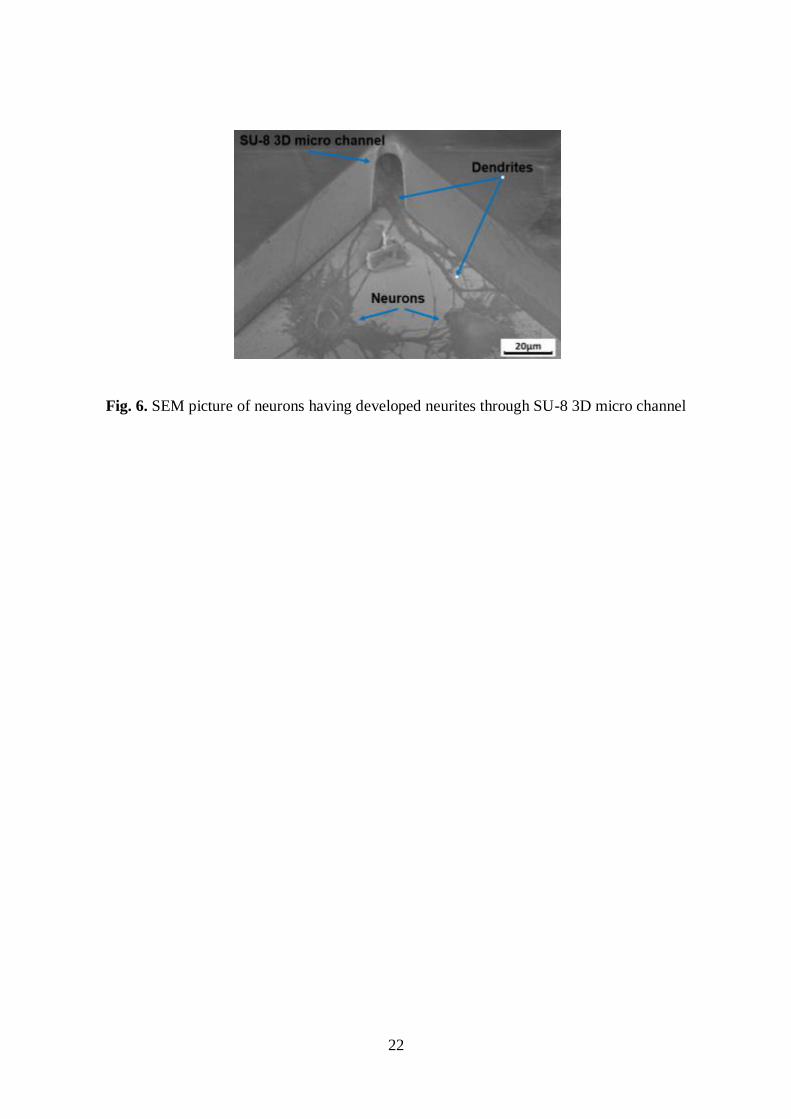
After the culture period, we used a protocol described above (cf. 2.5 and 2.6) to fix and dehydrate
neurons for SEM observations. Figure 6 illustrates neurons with neurites in the SU-8 micro-
channels and the absence of neurites growth on the micro-channels walls towards the SU-8 upper
layer (height: 50 m). Rat retina neuronal recording was tested using our FET filter system.
However, these specific neurons produce low voltage (~ 100 µV) [39] that could not be recorded by
our electronic interface. Indeed, even using an adapted electronic feedback control to reduce the
electrochemical noise [26], values around 500 µV were still obtained. In consequence, we could not
record neuronal activity from rat retina neurons. This is why we used snails' pedal neurons that
produce stronger signals.
8
3.2. Action potential recording from Lymnaea Stagnalis pedal neurons
Since the action potential of rat retina neurons was not compatible with our measurement noise,
the second aim of this work, namely to measure neuronal activity, was achieved with the use of
Lymnaea Stagnalis snail pedal neurons that are associated with higher voltage (> 10 mV). The
neurochips were functionalized as previously described and snail neuronal cells were cultured for
three days at room temperature (around 21°C) according to the previously described protocol (cf.
2.4). Viability test (cf. 2.5.) was realized to check the biocompatibility between snail neurons and
neurochip devices (Figure 7). As for mammalian neurons, snail neurons were deposited on the
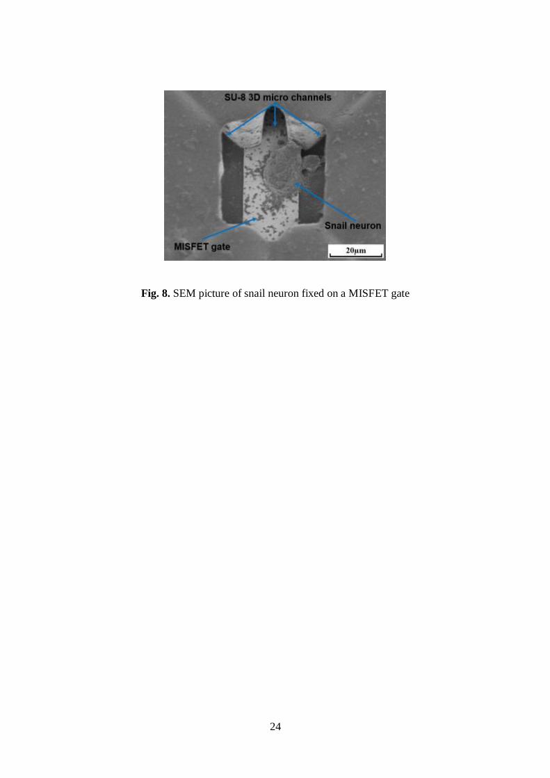
biosensor and survived easily with more than a 90% survival rate. After the cell fixation procedure
(cf. 2.6.), SEM observations revealed that the reception areas were well suited for this kind of
neuron cells since there was usually only a single cell by each electrode/gate (Figure 8). As a result,
measurement of a single cell was expected, even if, in some case, a second cell was also fixed on a
given MISFET gate. Neurites were again oriented by the SU-8 microstructures.
After the successful cell culture and guided growth, electrical measurements were made. An
output voltage of 0 V was measured in the resting state of the neurons and, except for the
measurement noise (~ 500 µV), no electrical signals were found without any neurons culture.
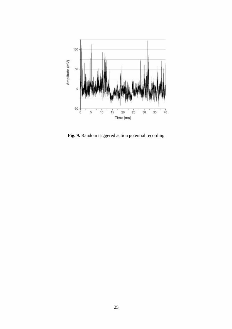
However, as soon as a neural network was grown on the neurochip, some occasional events were
measured with the difference between the maximal and the resting potential around 100 mV (figure
9). In 80% of our measurements, randomly triggered spiked-like events were recorded. In these
cases, the duration between the start of the depolarisation and the hyperpolarisation endpoint being
estimated to be around 7 ms. In the other cases, periodic electrical phenomena were evidenced.
According to literature [30-32,40], we assumed to have detected action potentials. Nevertheless, to
demonstrate that they events were truly neuronal spikes, we decided to use a "picrotoxin – GABA –
picrotoxin" protocol.
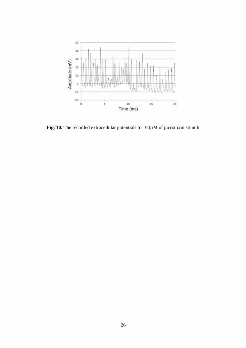
First, we applied picrotoxin in the bath to increase the firing frequency and the quality of the
recording signal. Figure 10 illustrates the change in spike-like events after applying picrotoxin.
Under the influence of the picrotoxin, the waveform of the spike-like events were greatly modified
as both the signal amplitude and its duration decreased to 30 mV and 0.5 ms respectively (Figure 11
a and b). The change observed after adding 100 µM of picrotoxin in the perfusion medium was not
seen during the first 30 seconds as expected since the picrotoxin must diffuse and activate the
neuronal GABAA receptors. After this delay of 30 seconds, action potentials were measured on the
MISFET channels and their frequency greatly increased one minute later. As a consequence,
neurons exhibited bursts of spike-like events with amplitude reaching 30 mV and a period around

9
0.5 ms (Figure 11). This time is defined as the so-called "spiking frequency" and is around 2000 Hz.
Picrotoxin was therefore responsible for an increase in the spiking frequency from 1 Hz (minimal
measurement value) to 2000 Hz. Five minutes after the picrotoxin injection, the analysed medium
was replaced by a new medium containing this time 100 µM of GABA. As for picrotoxin, GABA
diffusion required some time to activate GABAA receptors and to inhibit the neurons. After 30
seconds, the triggering frequency decreased progressively taking more than two minutes to washout
the picrotoxin effect returning neurons to their initial resting potential (0 V). Five minutes later, the
perfused medium was changed back to the picrotoxin containing solution. Again, neurons generated
some bursting events after one minute. The changes in the recorded signals when exchanging the
GABA inhibition with picrotoxin indicated that the MISFET biosensor measures effectively
neuronal activities.
4. Conclusion
In this study, we developed a MISFET transistor array to record neuronal activities while using
integrated SU-8 microfluidic structures in order to guide the neuronal growth. This lab-on-chip was
tested for the organized growth of rat retina neurons and Lymnaea Stagnalis snail pedal neurons.
Then, the MISFET array was used for the recording of action potentials while using Lymnaea
Stagnalis pedal neurons. Neuronal activities were successfully triggered and inhibited by
implementing a picrotoxin - GABA – picrotoxin successive injections protocol. The recorded
signals are consistent with recorded neuronal activities for snail neurons in culture demonstrating
thereby that our MISFET transistors can be used to measure neuronal activities.
Future works will concern the improvement of our "neurochip" platform. First of all, the
measurement noise has to be decreased drastically (< 50 µV) in order to be compatible with the
recording of mammals neurons and to be finally able to monitor action potentials from rat retina
neurons. This will be performed with the development of specific low-noise electronic interface,
either by improving the electronic feedback control to reduce the electrochemical noise, either by
increasing the acquisition data speed and using high-frequency filter to reduce the electronic noise.
So, the 16-MISFET neurochip will be used to analyse neural networks, aiming to the global
monitoring of electrophysiological signals. Secondly, the MISFET devices have to be replaced by
ISFET (Ion-Sensitive Field Effect transistor) devices in order to be able to monitor ionic
concentrations variations (focusing especially on the sodium Na+ and potassium K+ ions) on the
neuron surface and to correlate them with the neuronal activities. Finally, the "Stepper technology"
has still to be studied in order to optimize the mass fabrication of SU-8 3D micro-templates for the
neuronal growth.
10
Acknowledgments
Amel Bendali received a PhD fellowship from the University "Pierre and Marie Curie" (Paris
06). All authors were supported by a CNRS grant (programme interdisciplinaire: interface physique
chimie). Serge Picaud was supported by grants from the French "Fondation pour la Recherche
Médicale" (FRM) and by the European Community's Seventh Framework Programme (FP7) under
grant agreement n° 280433 (NEUROCARE project). The technological realizations and associated
research works were partly supported by the French RENATECH network.
References
[1] F.A. Edwards, A. Konnerth, B. Sakmann, T. Takahashi, "A thin slice preparation for patch
clamp recordings from neurones of the mammalian central nervous system", European Journal of
Physiology, 414 (1989) 600-612.
[2] O. Marre, A. Dario, N. Deshmukh, K. Sadeghi, F. Soo, T.E. Holy, M.J. Berry II, " Mapping a
complete neural population in the retina", Journal of Neurosciences, 32 (2012) 14859-73.
[3] M.E. Spira, A. Hai, "Multi-electrode array technologies for neuroscience and cardiology",
Nature Nanotechnology, 8 (2013) 83-94.
[4] F.O. Morin, Y. Takamura, E. Tamiya, "Investigating neuronal activity with planar
microelectrode arrays: achievements and new perspectives", Journal of Bioscience and
Bioengineering, 100 (2005) 131-143.
[5] C. Xie, Z. Lin, L. Hanson, Y. Cui, B. Cui B., "Intracellular recording of action potentials by
naopillar electroporation", Nature Nanotechnology 7 (2012) 185-190.
[6] Y. Nam, J. Chang, D. Khatami, G.J. Brewer, B.C. Wheeler, " Gold-coated microelectrode array
with thiol linked self-assembled monolayers for engineering neuronal cultures ", IEEE
Proceedings Nanobiotechnology, 151 (2004) 109–115.
[7] D. Ghezzi, M.R. Antognazza, M. Dal Maschio, E. Lanzarini, F. Benfenati, G. Lanzani, " A
hybrid bioorganic interface for neuronal photoactivation ", Nature Communications, 166 (2011)
1-7.
[8] G. Buzsáki, C.A. Anastassiou, C. Koch, "The origin of extracellular field and currents – EEG,
ECoG, LFP and spikes", Neuroscience, 13 (2012) 407-420.
[9] T. Cramer, B. Chelli, M. Murgia, M. Barbalinardo, E. Bystrenova, D.M. De Leeuw, F.
Biscarini, "Organic ultra-thin film transistors with a liquid gate for extracellular stimulation and

11
recording of electric activity of stem cell-derived neuronal networks", Physical Chemistry
Chemical Physics, 15 (2013) 3897-3905.
[10] L. Berdondini, K. Imfeld, A. Maccione, M. Tedesco, S. Neukom, M. Koudelka-Hep, S.
Martinoia, "Active pixel sensor array for high spatio-temporal resolution electrophysiological
recordings from single cell to large scale neuronal networks", Lab on a chip, 9 (2009) 2644-
2651.
[11] A. Hierlemann, U. Frey, S. Hafizovic, F. Heer, "Growing cells atop microelectronic chips:
Interfacing electrogenic cells in vitro with CMOS-based microelectrode arrays", Proceedings of
the IEEE, 99 (2011) 252-284.
[12] S. Herwik, S. Kisban, A. Aarts, K. Seidl, G. Girardeau, K. Benchenane, M.B. Zugaro, S.I.
Wiener, O. Paul, H.P. Neves, P. Ruther, "Fabrication technology for silicon-based microprobe
arrays used in acute and sub-chronic neural recording", Journal of Micromechanics and
Microengineering, 19 (2009) 1-11.
[13] J. Pine, "Recording action potentials from cultured neurons with extracellular microcircuit
electrodes", Journal of Neuroscience Methods, 2 (1980) 19-31.
[14] G.W. Gross, A.N. Williams, J.H. Luca, "Recording of spontaneous activity with photoetched
microelectrode surfaces from mouse signal neurons in culture", Journal of Neuroscience
Methods, 5 (1982) 13-22.
[15] P. Fromherz, "Electrical interfacing of nerve cells and semiconductor chips", ChemPhysChem,
3 (2002) 276-284.
[16] P. Fromherz, O. Müller, R. Weis, "Neuron transistor: electrical transfer function measured by
the patch-clamp technique", Physical Review Letters, 71 (1993) 4079-4082.
[17] P. Fromherz, A. Stett, "Silicon-neuron junction: capacitive stimulation of an individual neuron
on a silicon chip", Physical Review Letters, 75 (1995) 1670-1673.
[18] F. Patolsky, B. Timko, G. Yu, Y. Fang, A. Greytak, G. Zheng, C.M. Lieber, "Detection,
stimulation, and inhibition of neuronal signals with high-density nanowire transistor arrays",
Science, 313 (2006) 1100-1104.
[19] M. Jungblut, W. Knoll, C. Thielemann, M. Pottek, "Triangular neuronal network on
microelectrode arrays: an approach to improve the properties of low-density networks for
extracellular recording", Biomedical Microdevices, 11 (2009) 1269–1278.
[20] M.R. Hynd, J.P. Frampton, N. Dowell-Mesfin, J.N. Turner, W. Shain, "Directed cell growth on
protein-functionalized hydrogel surfaces", Journal of Neuroscience Methods, 162 (2007) 255–
263.

12
[21] N.S. Baek, J.-H. Lee, Y.H. Kim, B.J. Lee, G.H. Kim, I.-H. Kim, M.-A. Chung, S.-D. Jung,
"Photopatterning of cell-adhesive-modified poly(ethyleneimine) for guided neuronal growth",
Langmuir 27 (2011) 2717–2722.
[22] J. Wang, L. Ren, L. Li, W. Liu, J. Zhou, W. Yu, D. Tong, S. Chen, "Microfluidics: a new
cosset for neurobiology", Lab on a chip, 9 (2009) 644–652.
[23] J. Cheng, G. Zhu, L. Wu, X. Du, H. Zhang, B. Wolfrum, Q. Jin, J. Zhao, A. Offenhäusser, Y.
Xu, "Photopatterning of self-assembled poly(ethylene)glycol monolayer for neuronal network
fabrication", Journal of Neuroscience Methods, 213 (2013) 196-203.
[24] W.C. Chang, D.W. Sretavan, "Novel high-resolution micropatterning for neuron culture using
polylysine adsorption on a cell repellant, plasma-polymerized background", Langmuir 24 (2008)
13048–13057.
[25] I. Humenyuk, B. Torbiéro, S. Assié Souleille, R. Colin, X. Dollat, B. Franc, A. Martinez, P.
Temple-Boyer, "Development of pNH4-ISFET microsensors for water analysis",
Microelectronics Journal, 37 (2006) 475-479.
[26] F. Larramendy, F. Mathieu, S. Charlot, L. Nicu, P. Temple-Boyer, "Parallel detection in liquid
phase of N-channel MOSFET/ChemFET microdevices using saturation mode", Sensors and
Actuators B, 176 (2013) 379-385.
[27] F. Larramendy, L. Mazenq, P. Temple-Boyer, L. Nicu, "Three-dimensional close microfluidic
channels fabrication by stepper projection single step lithography: the diabolo effect", Lab on a
chip, 12 (2012) 387-390.
[28] J. Secco d’Aragona, "Dislocation etch for (100) planes in silicon", Journal of the
electrochemical society, 119 (1972) 948-952.
[29] B.A. Barres, B.E. Silverstein, D.P. Corey, L.L.Y. Chun, "Immunological, morphological, and
electrophysiological variation among retinal ganglion cells purified by panning", Neuron, 1
(1988) 791-803.
[30] M. Kyriakides, C.R. Mac Crhan, C.T. Slade, N.I. Syed, W. Winlow: "The morphology and
electrophysiology of the neurones of the paired pedal ganglia of Lymnae Stagnalis",
Comparative Biochemistry and Physiology 93 (1989) 861-876.
[31] R.L. Ridgway, N.I. Syed, K. Lukowiak, A.G.M. Bulloch, " Nerve growth factor (NGF) induces
sprouting of specific neurons of the snail Lymnaea stagnalis", Journal of Neurobiology, 22
(1991) 377-390.
[32] A.A. Prinz, P. Fromherz, "Electrical synapses by guided growth of cultured neurons from the
snail Lymnaea stagnalis", Biological Cybernetics, 82 (2000) L1-L5.
[33] M. Jenkner, B. Müller, P. Fromherz, "Interfacing a silicon chip to pairs of snail neurons
connected by electrical synapses", Biological Cybernetics, 84 (2001) 239-249.
13
[34] A. Cohen, M.E. Spira, S. Yitshaik, G. Borghs, O. Schwartzglass, J. Shappir, "Depletion type
floating gate p-channel MOS transistors for recording action potentials generated by cultured
neurons", Biosensors and Bioelectronics, 19 (2004) 1703-1709.
[35] F. Moccia, C. Di Cristo, W. Winlow, A. Di Cosmo, "GABAA-and AMPA-like receptors
modulate the activity of an identified neuron within the central pattern generator of the pond
snail Lymnaea stagnalis", Invertebrate Neuroscience, 9 (2009) 29-41.
[36] V.N. Vernekar, D.K. Cullen, N. Fogleman, Y. Choi, A.J. Garcia, M.G. Allen, G.J. Brewer,
M.C. La Placa, "SU‐8 2000 rendered cytocompatible for neuronal bioMEMS applications",
Journal of Biomedical Materials Research A, 89 (2008) 138-151.
[37] F. Walther, P. Davydovskaya, S. Zürcher, M. Kaiser, H. Herberg, A.M. Gigler, R.W. Stark,
"Stability of the hydrophilic behavior of oxygen plasma activated SU-8", Journal of
Micromechanical Microengineering, 17 (2007) 524-531.
[38] L. Qiana, W.M. Saltzman, "Improving the expansion and neuronal differentiation of
mesenchymal stem cells through culture surface modification", Biomaterials, 25 (2004) 1331–
1337.
[39] B. Kolomiets, E. Dubus, M. Simonutti, S. Rosolen, J.A. Sahel, S. Picaud, "Late histological
and functional changes in the P23H rat retina after photoreceptor loss", Neurobiology of Disease,
38 (2010) 47-58.
[40] G.E. Spencer, N.I. Syed, K. Lukowiak, "Neural changes after operant conditioning of the aerial
respiratory behaviour in Lymnae Stagnalis", The journal of neuroscience, 19 (1999) 1835-1843.
Biographies
Florian Larramendy was born in Brive-la-Gaillarde, France, in 1986. He received the M.S. degree
in Microelectronic System Engineering from the Paul Sabatier University, Toulouse, France, in
2009. He joined the Laboratory for Analysis and Architecture of Systems (LAAS), National Center
of Scientific Research (CNRS), Toulouse in 2009 as PhD Student. He was in charge of the
development of microsystems to measure neuronal activities. After obtaining his D. Sc. Degree in
2013, he joined the EUJO-LIMMS project in the Microsystem Materials Laboratory, Department of
Microsystems Engineering (IMTEK), Freiburg, Germany, and the Laboratory for Integrated Micro
Mechatronic Systems (LIMMS), Tokyo, Japan. Currently, he is in charge of the development of
microprobes for brain insertion for biomedical applications.
14
Amel Bendali received her BS degree in Physics in 2006 and her MS degree in Instrumentation for
Biotechnology in 2008 from Institut National Polytechnique de Grenoble, France. She recently
graduated her PhD in Neuroscience at Université Paris VI under the supervision of Dr Serge Picaud.
Her research focuses on building networks of retinal neurons on multi-electrode arrays for the study
of retinal signal processing and testing carbon-based materials such as diamond and graphene to
design retinal prosthetic devices.
Marie Charline Blatché was born in Toulouse, France, in 1986. She received the Licence degree in
Biotechnologies from Nice-Sophia Antipolis University, Nice, France in 2008. She joined the
Laboratoire d’Analyse et d’Architecture des Systèmes (LAAS), Centre National de la Recherche
Scientifique (CNRS), Toulouse in 2009, where she is in charge of the "Biology" technological
platform and worked on the development of cell growth on microsystems.
Fabrice Mathieu was born in Orléans, France, in 1972. He received the engineering degree in
communication systems and electronics from the CNAM (Conservatoire National des Arts et
Métiers), Toulouse, France, in 2003. He joined the Laboratoire d’Analyse et d’Architecture des
Systèmes (LAAS), Centre National de la Recherche Scientifique (CNRS), Toulouse, in 2001, where
he is currently in charge of the development and design of very low signal detection systems
applied to the micro(nano)electromechanical systems area and its complete electronic treatment and
control for automation.
Serge Picaud was born in Paris (France) in 1961. He received a PhD in Neurosciences from the
University of Marseille in 1990. He was educated by leaders in the field of retinal physiology
during doctoral and postdoctoral stays with Professor Wässle (Max-Planck Institute for Brain
research, Francfurt, Germany) and Prpfessor Werblin (University of California, Berkeley, USA). He
is currently leading the team “retinal information processing” at the Vision Institute in Paris created
by Professor Sahel. After studying retinal physiology and pharmacology with applications in
neuroprotection, the team has moved toward strategies for restoring vision in blind patients having
lost their photoreceptors. These strategies involve retinal prostheses or optogenetic therapy, which
requires expression of photosensitive pump or ionic channels in selected retinal neurones.
Pierre Temple-Boyer was born in Montpellier (France) in 1966. He received his Engineer Master’s
Degree in electronic engineering from the Ecole Supérieure d'Electricité (Paris – France) in 1990
and his Master’s Degree in microelectronics from the Université Paul Sabatier de Toulouse
(France) in 1992. He joined the Laboratoire d'Architecture et d'Analyse des Systèmes of the French

15
Centre National de la Recherche Scientifique (LAAS-CNRS) in 1992 and received the PhD degree
from the Institut National des Sciences Appliquées de Toulouse (France) in 1995. Since then, as a
senior researcher, he has been working on the development of micro- and nanotechnologies.
Liviu Nicu was born in 1973 in Bucharest (Romania). After completing his Master of Electrical
Engineering at the Paul Sabatier University of Toulouse (France) in 1997, he joined the Integrated
Microsystems Group at the LAAS (Laboratory for Analysis and Architecture of Systems) of
Toulouse where he obtained his Ph.D. in 2000 into the Micromechanical Structures field. From
2000 to 2003, he was R&D Engineer at Thales Avionics, Valence (France). His activities focused
onto the development of micromechanical sensors for the civil and military navigation applications.
Since 2003 he joined the NanoBioSystems Group at LAAS as a full time CNRS (National Center of
Scientific Research) researcher where he currently works in two main research fields: the
development of (1) new resonant bio(chemical)sensors using M(N)EMS technologies and of (2)
cantilever-based microsystems for contact deposition of small amounts of biological samples for
biochip applications.
16
FIGURE CAPTIONS
Fig. 1. Schematic of the SiO2/Si3N4/Ti/Au MISFET device
Fig. 2. Picture of SU-8 3D micro-channel fabricated using the “Stepper technology” on a MISFET
Fig. 3. Optical microscopy photographs of a) (left) the 16 MISFET array and its associated SU-8
3D microfluidic network and b) (right) the neurochip bearing the SU-8 microfluidics
Fig. 4. Confocal microscopy photograph of neurons network
developed through SU-8 3D microfluidic structures
Fig. 5. Fluorescence picture of calcein-stained viable neurons
and their outgrowths in culture on MISFETs and across SU-8 3D micro channels
Fig. 6. SEM picture of neurons having developed neurites through SU-8 3D micro channel
Fig. 7. Fluorescence observed of a) live cells and b) dead cells on biosensor
Fig. 8. SEM picture of two snail neurons fixed on a MISFET gate
Fig. 9. Random triggered action potential recording
Fig. 10. The recorded extracellular potentials to 100µM of picrotoxin stimuli
Fig. 11. "Spike type" complete waveform of recorded neuron potentials
a) without and b) with 100 µM of picrotoxin
17
Fig. 1. Schematic of the SiO2/Si3N4/Ti/Au MISFET device
18
Fig. 2. Picture of SU-8 3D micro-channel fabricated using the “Stepper technology” on a MISFET
19
Fig. 3. Optical microscopy photographs of a) (left) the 16 MISFET array and its associated SU-8
3D microfluidic network and b) (right) the neurochip bearing the SU-8 microfluidics
20
Fig. 4. Confocal microscopy photograph of neurons network
developed through SU-8 3D microfluidic structures

21
Fig. 5. Fluorescence picture of calcein-stained viable neurons
and their outgrowths in culture on MISFETs and across SU-8 3D micro channels
22
Fig. 6. SEM picture of neurons having developed neurites through SU-8 3D micro channel

23
a) b)
Fig. 7. Fluorescence observed of a) live cells and b) dead cells on biosensor
24
Fig. 8. SEM picture of snail neuron fixed on a MISFET gate
25
Fig. 9. Random triggered action potential recording
26
Fig. 10. The recorded extracellular potentials to 100µM of picrotoxin stimuli

27
Fig. 11. "Spike type" complete waveform of recorded neuron potentials
a) without and b) with 100 µM of picrotoxin