mitigating parameter variation with dynamic fine-grain...
TRANSCRIPT

Mitigating Parameter Variation with Dynamic Fine-Grain Body Biasing*
Radu Teodorescu, Jun Nakano, Abhishek Tiwari and Josep Torrellas
University of Illinois at Urbana-Champaign
*to appear in MICRO-40, December 2007
http://iacoma.cs.uiuc.edu
Tuesday, October 9, 2007

Radu Teodorescu Intel PhD Fellowship Forum, October 2007
Intel Corp.
Motivation
2
• Technology scaling continues
• More and more transistors every generation!
• However...
• Chips are increasingly affected by parameter variation
Tuesday, October 9, 2007

Radu Teodorescu Intel PhD Fellowship Forum, October 2007
Parameter Variation
• Process variation
• Manufacturing at low feature sizes
• Temperature variation
• Uneven activity distribution
• Supply voltage variation
• IR drop, di/dt noise
3
23
Sources of VariationsSources of Variations
0
50
100
150
200
250
He
at
Flu
x (
W/c
m2
)Heat Flux (W/cm2)—Vcc variation
40
50
60
70
80
90
100
110
Te
mp
era
ture
(C
)
Temp Variation & Hot spots
10
100
1000
10000
1000 500 250 130 65 32
Technology Node (nm)
Mean
Nu
mb
er
of
Do
pan
t
Ato
ms
Random Dopant Fluctuations
0.01
0.1
1
1980 1990 2000 2010 2020
micron
10
100
1000
nm193nm193nm248nm248nm
365nm365nmLithographyLithography
WavelengthWavelength
65nm65nm
90nm90nm
130nm130nm
GenerationGeneration
GapGap
45nm45nm
32nm32nm
13nm13nm
EUVEUV
180nm180nm
Source: Mark Bohr, Intel
Sub-wavelength Lithography
!
"#$"%&'()*(+
,+(*-$.*(+
/#01234)#2.*(+
"
.
5
66627
"
8*)&9:$
;*:9(%&+ <=4
>?$:@
A>$:@
A?$:@
"#.+ "B5
"()*#:+C$
"#-#D9:
"#.+ "B5
"()*#:+C$
"#-#D9:
E?$:@!>$:@
F>$:@AG$:@
G??FG??!
G??HG?I?
G?IGJ
4+D1:9-90K$.+:+)*(#9:
G?$:@I?$:@
5 nm5 nm
>$:@
;*:9L#)+
,*:%M*D(%)#:0$$$$$$$$$$$$5+N+-9O@+:($$$$$$$$$$$$$$$$$$$$$$$$$P+'+*)D1
8,Q"$P+'+*)D1$89:(#:%+'8,Q"$P+'+*)D1$89:(#:%+'RR
Intel Corp.
Tuesday, October 9, 2007

Radu Teodorescu Intel PhD Fellowship Forum, October 2007
Effects of Parameter Variation
• Higher power consumption
• Lower frequency
• Uncertainty in the design process
4
Tuesday, October 9, 2007

Radu Teodorescu Intel PhD Fellowship Forum, October 2007
Outline
• A Model of Process Variation
• Dynamic Fine-Grain Body Biasing
• Evaluation
• Conclusions
5
Tuesday, October 9, 2007
Radu Teodorescu Intel PhD Fellowship Forum, October 2007
Outline
• A Model of Process Variation
• Dynamic Fine-Grain Body Biasing
• Evaluation
• Conclusions
6
Tuesday, October 9, 2007

Radu Teodorescu Intel PhD Fellowship Forum, October 2007
• Fast, simple and parameterizable model
• We model two key process parameters:
• Transistor critical dimension (Leff) and threshold voltage (Vth)
• We also model temperature effects
7
A Model For Process Variation
Tuesday, October 9, 2007
Radu Teodorescu Intel PhD Fellowship Forum, October 2007
Variation Components
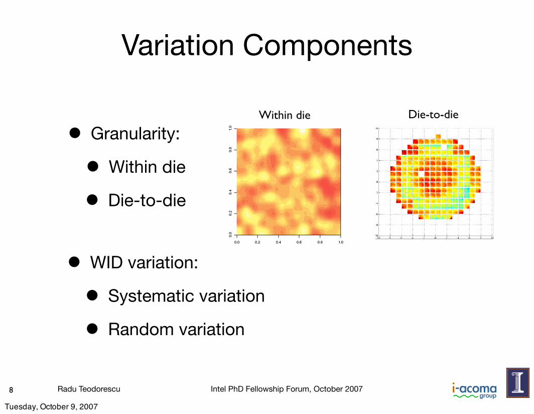
• Granularity:
• Within die
8
!!
"#$%&''()*#+*,+$-"#$%&''()*#+*,+$-
!! !"#$#"$%"#!"#$#"$%"#
!! &'("))$*+,-(&'("))$*+,-(
!! ././0012-12-
Die-to-dieWithin die
• WID variation:
• Systematic variation
• Random variation
• Die-to-die
Tuesday, October 9, 2007

Radu Teodorescu Intel PhD Fellowship Forum, October 20079
A Model For Process Variation
ΔP = ΔPD2D + ΔPWID = ΔPD2D + ΔPrand + ΔPsys
• Variation in any parameter P:
• We focus on WID variation
• D2D is a chip-wide offset to ΔPWID
• Random and systematic components
• Modeled as normal distributions
• Treated separately - impact different levels of the microarchitecture
Tuesday, October 9, 2007

Radu Teodorescu Intel PhD Fellowship Forum, October 2007
Systematic Variation
• Characterized by a correlation function:
10
• Correlation is position independent and isotropic
• For ρ(r) we choose the spherical model
parameter P (eg. Vth or Leff), can be represented as follows:
∆P = ∆PD2D + ∆PWID = ∆PD2D + ∆Prand + ∆Psys
In this work, we focus on WID variation, but D2D variation is easily modeled: One needs only add a random chip-wide offset
to the parameters of every transistor on the die. For simplicity, we model the random and systematic components of WID variation
as normal distributions [13, 26]. We treat random and systematic variation separately, since they arise from different physical
phenomena. As described in [26], we assume that their effects are additive.
3.1 Systematic Variation
Several methods of modeling the spatial correlation structure of systematic variation have been proposed. For example,
[18, 26] use a quad tree model that recursively partitions the die into four parts. In this paper, we use a different method that
models systematic variation using a multivariate normal distribution with a spherical correlation structure. We divide a chip into n
small, equally-sized rectangular sections. The value of the systematic component of Vth and Leff is assumed to be constant within
each section.
For simplicity, we assume that systematic variation is position-independent and isotropic; given two points !x and !y on the
die, the correlation of their systematic variation values depends only on the distance between !x and !y. These assumptions closely
match the empirical data obtained by Friedberg et al. [11], but they do fail to capture some important anisotropic effects (eg. mask
misalignment) and position-dependent effects (eg. CMP dishing). Assuming position independence and isotropy, the correlation
function of a systematically-varying parameter P is:
corr(P!x, P!y) = "(r) ; r = |!x! !y|
By definition, "(0) = 1 (i.e., totally correlated). Intuitively, "(") = 0 (i.e., totally uncorrelated). To specify the behavior of
"(r) between the limits, we choose the spherical model [8], which is in close agreement with Friedberg’s measured data [11]:
"(r) =
1! 3r2φ + r3
2φ3 : (r # #)
0 : otherwise
(7)
Figure 1 plots the function "(r). At a finite distance #, the correlation converges to zero, while at small distances, the
correlation is approximately proportional to distance. A large # implies that large sections of the chip are correlated with each
other; the opposite is true a small #. All # values in this work are specified as a fraction of the largest die dimension. As an
illustration, Figure 2 shows example parameter value map for # = 0.5 and # = 0.1. These maps were generated with the geoR
5
• Multivariate normal distribution (μsys=0, σsys)
Px
Py
r
• We divide the chip into a grid of points
• Each point has one random value of ΔPsys
Tuesday, October 9, 2007

Radu Teodorescu Intel PhD Fellowship Forum, October 2007
Spherical Model
• Matches measured data [Friedberg et al. 05]
11
0
1
0 φr
(r)ρ
Figure 1: Correlation of systematic parameters at two points as a function of the distance r between them.
Figure 2: Example spatial variation maps for a parameter with φ = 0.1 (left) and φ = 0.5 (right).
7
parameter P (eg. Vth or Leff), can be represented as follows:
∆P = ∆PD2D + ∆PWID = ∆PD2D + ∆Prand + ∆Psys
In this work, we focus on WID variation, but D2D variation is easily modeled: One needs only add a random chip-wide offset
to the parameters of every transistor on the die. For simplicity, we model the random and systematic components of WID variation
as normal distributions [13, 26]. We treat random and systematic variation separately, since they arise from different physical
phenomena. As described in [26], we assume that their effects are additive.
3.1 Systematic Variation
Several methods of modeling the spatial correlation structure of systematic variation have been proposed. For example,
[18, 26] use a quad tree model that recursively partitions the die into four parts. In this paper, we use a different method that
models systematic variation using a multivariate normal distribution with a spherical correlation structure. We divide a chip into n
small, equally-sized rectangular sections. The value of the systematic component of Vth and Leff is assumed to be constant within
each section.
For simplicity, we assume that systematic variation is position-independent and isotropic; given two points !x and !y on the
die, the correlation of their systematic variation values depends only on the distance between !x and !y. These assumptions closely
match the empirical data obtained by Friedberg et al. [11], but they do fail to capture some important anisotropic effects (eg. mask
misalignment) and position-dependent effects (eg. CMP dishing). Assuming position independence and isotropy, the correlation
function of a systematically-varying parameter P is:
corr(P!x, P!y) = ρ(r) ; r = |!x− !y|
By definition, ρ(0) = 1 (i.e., totally correlated). Intuitively, ρ(∞) = 0 (i.e., totally uncorrelated). To specify the behavior of
ρ(r) between the limits, we choose the spherical model [8], which is in close agreement with Friedberg’s measured data [11]:
ρ(r) =
1− 3r2φ + r3
2φ3 : (r ≤ φ)
0 : otherwise
(7)
Figure 1 plots the function ρ(r). At a finite distance φ, the correlation converges to zero, while at small distances, the
correlation is approximately proportional to distance. A large φ implies that large sections of the chip are correlated with each
other; the opposite is true a small φ. All φ values in this work are specified as a fraction of the largest die dimension. As an
illustration, Figure 2 shows example parameter value map for φ = 0.5 and φ = 0.1. These maps were generated with the geoR
5
Px
Py
r
Stronger correlation
Px
Py
r
Weaker correlation
Tuesday, October 9, 2007

Radu Teodorescu Intel PhD Fellowship Forum, October 2007
Random Variation
• Random variation - transistor level
• We model it analytically as a normal distribution
• Both ΔPrand and ΔPsys are normal and independent with σrand and σsys
12
statistics package [24], as were all other maps in our experiments.
For delay estimation, the systematic parameters we are concerned with are Leff and Vth. The ITRS report [1] tells us that the
total standard deviation of Leff is roughly half of that of Vth. We thus make the approximation that Leff is normally distributed
with a total σ equal to half of that of Vth. Moreover, according to [5], the systematic component of Leff is strongly correlated
with the systematic component of Vth. Hence, we use the following equation to generate a value of the systematic component of
Leff given the value of the systematic component of Vth. Let L0eff be the nominal value of the effective length and let V
0th be the
nominal value of the threshold voltage. We use:
Leff = L0eff
!1 +
Vth ! V 0th
2V 0th
"(8)
3.2 Random Variation
Random variation occurs at a much finer granularity than systematic variation— at the level of individual transistors. Hence, it
is not possible to model random variation in the same explicit way as systematic variation — by simulating a grid where each cell
has its own parameter values. Instead, random variation appears in the model analytically. We assume that the random components
of Vth and Leff are both normally distributed with zero mean. Each has a different σ, however. Further, for ease of analysis, we
assume that the random Vth and Leff values for each transistor are uncorrelated (independently distributed).
3.3 Values for µ, σ and φ
Using the model for systematic variation described, we can compute the value of the systematic components for each of the
grid points. Because the random and systematic components are additive, we can express the mean and standard deviation of the
total WID variation as follows. Since the random and systematic components are normal and independently distributed, their sum
is also normal as follows. This applies to both Vth and Leff:
µtotal = µrand + µsys
σtotal =#
σ2rand + σ2
sys
(9)
To specify the individual variation parameters, we start with the assumption that for Vth, σtotal = 0.09µtotal. Moreover,
according to empirical data gathered by [16], the random and systematic components are approximately equal in 32 nm technology.
Hence, we assume that they have equal variances. Since both components are modeled as normal distributions, Equation 9 tells
us that their standard deviations σrand and σsys are equal to 9%/"
2 = 6.3% of the mean. This value for the random component
matches the empirical data of Keshavarzi et al. [17]. Moreover, Equation 8 completely specifies the systematic Leff values in terms
of the Vth values, giving a standard deviation of systematic Leff that is 3.2% of L0eff. Next, assuming again that the random and
systematic components of variation are more or less equal, we have that σrand and σsys for Leff are both equal to 3.2% of the
6
Tuesday, October 9, 2007

Radu Teodorescu Intel PhD Fellowship Forum, October 2007
Outline
• A Model of Process Variation
• Dynamic Fine-Grain Body Biasing
• Evaluation
• Conclusions
13
Tuesday, October 9, 2007

Radu Teodorescu Intel PhD Fellowship Forum, October 2007
Body Biasing
• Well known technique for Vth control
• A voltage is applied between source/drain and substrate of a transistor
• Forward body bias
• Reverse body bias
14
RBB - Vth ↑ - Freq ↓ - Leak ↓
FBB - Vth ↓ - Freq ↑ - Leak ↑
• Useful knob to control frequency and leakage
Tuesday, October 9, 2007

Radu Teodorescu Intel PhD Fellowship Forum, October 2007
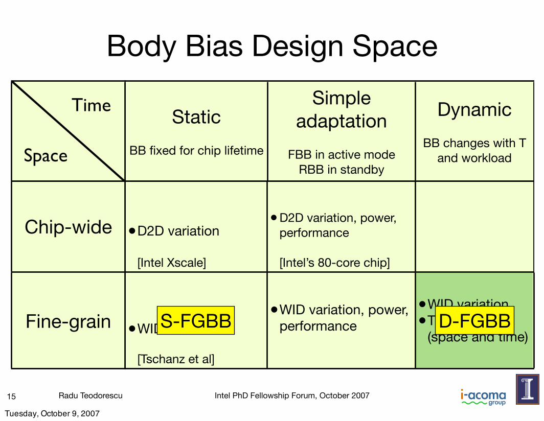
•D2D variation
[Intel Xscale]
•D2D variation, power, performance
[Intel’s 80-core chip]
•WID variation
[Tschanz et al]
•WID variation, power, performance
•WID variation•T variation
(space and time)
Static
BB fixed for chip lifetime
Simple adaptation
FBB in active modeRBB in standby
Dynamic
BB changes with T and workload
Chip-wide
Fine-grain
Body Bias Design Space
15
Space
Time
Tuesday, October 9, 2007

Radu Teodorescu Intel PhD Fellowship Forum, October 2007
•D2D variation
[Intel Xscale]
•D2D variation, power, performance
[Intel’s 80-core chip]
•WID variation
[Tschanz et al]
•WID variation, power, performance
•WID variation•T variation
(space and time)S-FGBB
Static
BB fixed for chip lifetime
Simple adaptation
FBB in active modeRBB in standby
Dynamic
BB changes with T and workload
Chip-wide
Fine-grain
Body Bias Design Space
15
Space
Time
Tuesday, October 9, 2007
Radu Teodorescu Intel PhD Fellowship Forum, October 2007
•D2D variation
[Intel Xscale]
•D2D variation, power, performance
[Intel’s 80-core chip]
•WID variation
[Tschanz et al]
•WID variation, power, performance
•WID variation•T variation
(space and time)S-FGBB D-FGBB
Static
BB fixed for chip lifetime
Simple adaptation
FBB in active modeRBB in standby
Dynamic
BB changes with T and workload
Chip-wide
Fine-grain
Body Bias Design Space
15
Space
Time
Tuesday, October 9, 2007

Radu Teodorescu Intel PhD Fellowship Forum, October 2007
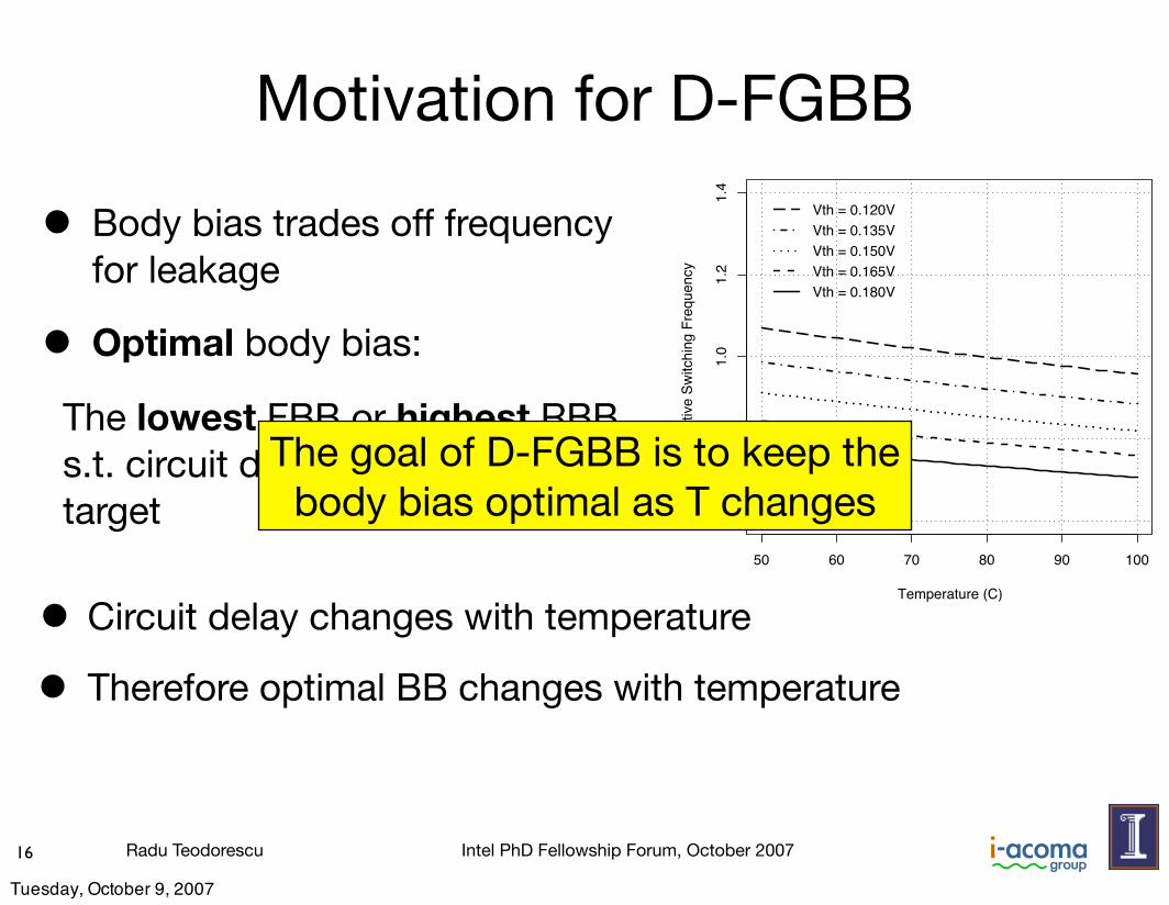
Motivation for D-FGBB
• Body bias trades off frequency for leakage
• Optimal body bias:
The lowest FBB or highest RBB s.t. circuit delay meets frequency target
16
50 60 70 80 90 100
0.6
0.8
1.0
1.2
1.4
Temperature (C)
Rela
tive
Switc
hing
Fre
quen
cy
Vth = 0.180VVth = 0.165VVth = 0.150VVth = 0.135VVth = 0.120V
• Circuit delay changes with temperature
• Therefore optimal BB changes with temperature
Tuesday, October 9, 2007
Radu Teodorescu Intel PhD Fellowship Forum, October 2007
Motivation for D-FGBB
• Body bias trades off frequency for leakage
• Optimal body bias:
The lowest FBB or highest RBB s.t. circuit delay meets frequency target
16
50 60 70 80 90 100
0.6
0.8
1.0
1.2
1.4
Temperature (C)
Rela
tive
Switc
hing
Fre
quen
cy
Vth = 0.180VVth = 0.165VVth = 0.150VVth = 0.135VVth = 0.120V
• Circuit delay changes with temperature
• Therefore optimal BB changes with temperature
The goal of D-FGBB is to keep the body bias optimal as T changes
Tuesday, October 9, 2007

Radu Teodorescu Intel PhD Fellowship Forum, October 2007
Finding the Optimal BB
• Measure the delay of each BB cell
• Critical path replicas to sample cell delay
17
Critical Path
Replica
Phase
Detectorextradelay
fast
slow
RBB
FBB
Sample Point
CLK
• Phase detector “times” the critical path replica
• If slow - FBB signal raised
• If fast - RBB signal raised
Tuesday, October 9, 2007

Radu Teodorescu Intel PhD Fellowship Forum, October 200718
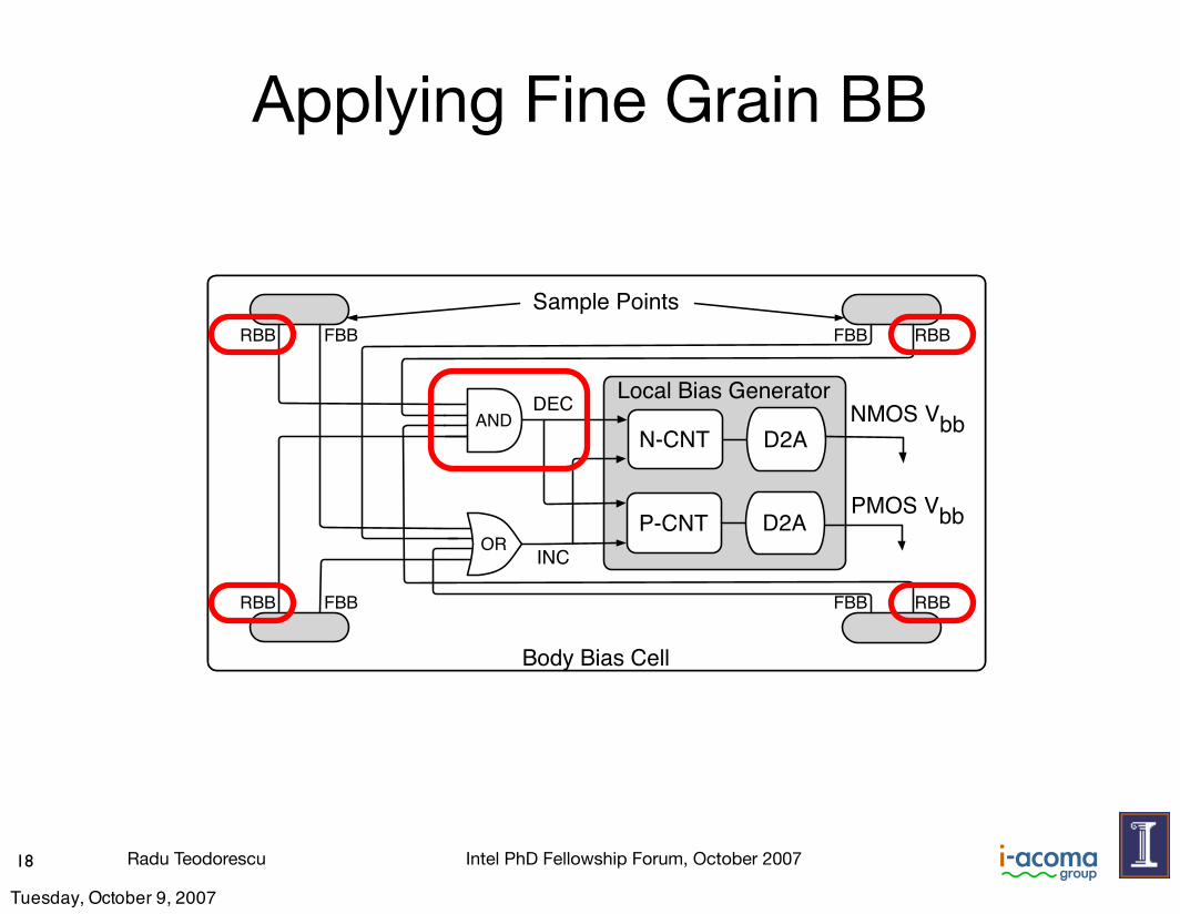
Body Bias Cell
RBB FBB
RBB
RBB
RBBFBB
FBB
FBB
Sample Points
Local Bias Generator
N-CNT
P-CNT
Local Bias Generator
N-CNT
P-CNT D2A
D2A
NMOS Vbb
PMOS Vbb
Body Bias Cell
Local Bias Generator
N-CNT
P-CNT D2A
D2AAND
OR
DEC
INC
RBB FBB
RBB
RBB
RBBFBB
FBB
FBB
NMOS Vbb
Sample Points
PMOS Vbb
Applying Fine Grain BB
Tuesday, October 9, 2007
Radu Teodorescu Intel PhD Fellowship Forum, October 200718
Body Bias Cell
RBB FBB
RBB
RBB
RBBFBB
FBB
FBB
Sample Points
Local Bias Generator
N-CNT
P-CNT
Local Bias Generator
N-CNT
P-CNT D2A
D2A
NMOS Vbb
PMOS Vbb
Body Bias Cell
Local Bias Generator
N-CNT
P-CNT D2A
D2AAND
OR
DEC
INC
RBB FBB
RBB
RBB
RBBFBB
FBB
FBB
NMOS Vbb
Sample Points
PMOS Vbb
Applying Fine Grain BB
Tuesday, October 9, 2007

Radu Teodorescu Intel PhD Fellowship Forum, October 2007
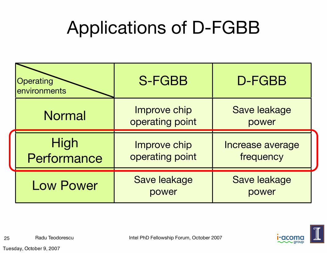
Applications of D-FGBB
19
S-FGBB D-FGBB
Normal Improve chip operating point
Save leakage power
High Performance
Improve chip operating point
Increase average frequency
Low Power Save leakagepower
Save leakagepower
Operating environments
Tuesday, October 9, 2007

Radu Teodorescu Intel PhD Fellowship Forum, October 2007
S-FGBB D-FGBB
Normal Improve chip operating point
Save leakage power
High Performance
Improve chip operating point
Increase average frequency
Low Power Save leakagepower
Save leakagepower
Applications of D-FGBB
20
Operating environments
Tuesday, October 9, 2007
Radu Teodorescu Intel PhD Fellowship Forum, October 2007
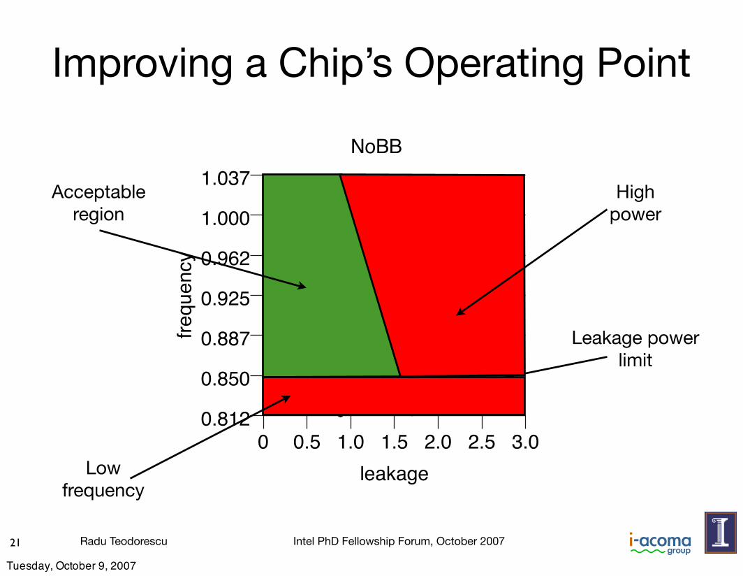
Improving a Chip’s Operating Point
21
NoBB
(a)
0 0.5 1.0 1.5 2.0 2.5 3.0leakage
0.8120.8500.8870.9250.9621.0001.037
ycneuqerf
0 0.5 1.0 1.5 2.0 2.5 3.0leakage
0.8120.8500.8870.9250.9621.0001.037
S-FGBB1
(b)
0 0.5 1.0 1.5 2.0 2.5 3.0leakage
0.8120.8500.8870.9250.9621.0001.037
S-FGBB16
(c)
0 0.5 1.0 1.5 2.0 2.5 3.0leakage
0.8120.8500.8870.9250.9621.0001.037
S-FGBB64
(d)
0 0.5 1.0 1.5 2.0 2.5 3.0leakage
0.8120.8500.8870.9250.9621.0001.037
S-FGBB144
(e)
Figure 10. Frequency versus leakage power for a batch of 200 chips at Tcal and full load under various schemes.
0.03 0.06 0.09 0.120
0.20.40.60.81.01.2
Freq
uenc
y
(a)
0.03 0.06 0.09 0.120
0.20.40.60.81.01.21.41.61.8
Leak
age P
ower
!=0.1 !=0.2 !=0.5
(b)"/# "/#
Figure 11. Impact of Vth variation on the chip’s frequency (a)and leakage power (b).
“fall” on the hottest region of the chip, the chip is likely to have lowfrequency. On the other hand, if many transistors with very low Vthfall on the hottest area, the chip is likely to have high leakage.We see two main trends. First, across chips in one experiment,
leakage varies more than frequency — since leakage is exponentialwith T, an unfavorable Vth distribution can significantly increaseleakage power. Second, as ! decreases, the average frequency de-creases as well. The reason is that, given a set of high-Vth transis-tors, if they are uniformly spread out in the chip (low !), there is ahigher chance that some will fall on the hottest region of the chip,thus reducing the chip’s frequency.
7.2. Normal Operation: D-FGBB Improves aChip’s Operating Point
S-FGBB can be used to tune the chips in a batch so that they fallinto desirable frequency-leakage bins [45]. The goal is to place eachchip at the highest possible frequency bin where it still meets thepower consumption constraint. In this section, we summarize theimpact of S-FGBB and then show how D-FGBB further improvesa chip’s operating point.The Acceptable Region for a chip [45] is bounded by two con-
ditions: (i) the frequency should be higher than a given minimumvalue, and (ii) the sum of dynamic and leakage power should beless than a given maximum value. In a frequency-leakage plot suchas Figure 10(a), these constraints require that the chip be above ahorizontal line and to the left of a slanted line, respectively. Theslanted line has this shape because, as frequency increases, the dy-namic power increases linearly and, therefore, the amount of tolera-ble leakage power decreases linearly. Inside the Acceptable Region,higher frequency is better.Figure 10(a) shows a scatter plot of the frequency and leak-
age power for our 200 chips, with axes normalized to NoVar (noprocess-induced Vth variation). We build the slanted line so that it
would include the NoVar chip, which is point (1,1). We then arbi-trarily set the horizontal line to 0.85 of the frequency of the NoVarchip, and divide the range into four equally-spaced frequency bins.As a fraction of the NoVar frequency, the ranges of the bins are:0.850–0.887, 0.887–0.925, 0.925–0.962, and over 0.962. Thesebins are in the ballpark of those used in commercial processors.7.2.1. Impact of S-FGBBIn Figure 10(a), some chips fall outside the Acceptable Region.
By applying S-FGBB to a chip, we can move it into the Accept-able Region or, if it is already there, move it to a higher frequencypoint. Using the axes and the slanted line of Figure 10, Figure 12graphically shows the impact of our S-FGBB calibration algorithmof Section 4.2.
at Tavg
at Tcalat Tcal
calS!FGBB at T
Fcal
Leakage Power
CA’
A
BD!FGBB
D
Freq
uenc
y
Leakage limit Original chip
S!FGBB
Figure 12. Impact of S-FGBB and D-FGBB on a chip’soperating point.
Consider a chip that is originally operating at point A. Our al-gorithm can move the chip along the curve labeled S-FGBB atTcal. The result of the algorithm is to bring the chip to point B,at frequency Fcal, where the chip dissipates the maximum allowedpower — thus, point B is on the slanted line. Point B is more desir-able than A in that it is inside the Acceptable Region and is poten-tially in a higher frequency bin than A. Increasing the frequency be-yond Fcal would push the chip to the left of the slanted line, wherepower consumption is excessive. In cases where the original chip isoperating at point A’, the S-FGBB algorithm reduces the frequencyand brings it to point B.The actual curve followed from A depends on the number of
FGBB cells. The schemes with more cells such as FGBB144 targettheir BB voltages better and push the chip to a B position that ishigher in the slanted line — thus delivering chips in better bins.To show it, we take the batch of chips of Figure 10(a) and apply
our S-FGBB algorithm using the FGBB1, FGBB16, FGBB64, andFGBB144 schemes. The resulting frequency-leakage scatter plotsare shown in Figures 10(b)-(e). The charts show that all the schemes
Acceptable region
Leakage power limit
High power
Lowfrequency
Tuesday, October 9, 2007

Radu Teodorescu Intel PhD Fellowship Forum, October 2007
• Post-manufacturing calibration phase:
1. Bring chip to Tcal
2. Set target frequency Fcal0, and run at full load
3. BB is adjusted automatically
4. Measure total power Pcal: if Pcal<Ptarget, Fcal1=Fcal0++, else Fcal1=Fcal0--
5. Repeat if needed, until Pcal ≈ Ptarget
• Fcali becomes the chip’s frequency
22
Improving a Chip’s Operating Point
Tuesday, October 9, 2007

Radu Teodorescu Intel PhD Fellowship Forum, October 2007
D-FGBB Adapts to Changes in T
• Calibration temperature Tcal is conservative
• Average T much lower:
23
IntQ
IntRe
gLd
StQ
IntEx
ecInt
Map
DTB
ITB
FPQ
FPRe
gFP
Map
Bpre
dFP
Add
FPMu
lDc
ache
Icach
eL2
Cach
e
Functional Units
0
20
40
60
80
100
Tem
pera
ture
(C)
Tmax TavgTcal
Tuesday, October 9, 2007

Radu Teodorescu Intel PhD Fellowship Forum, October 200724
Freq
uenc
y
Leakage
Leakagelimit at Tcal
Fcal S-FGBB at Tcal
S-FGBB at Tavg
D-FGBB at Tavg
Original chip
D-FGBB Saves Leakage Power
• S-FGBB finds and sets Fcal
• D-FGBB adjusts dynamically to T changes to save power while running at Fcal
Tuesday, October 9, 2007
Radu Teodorescu Intel PhD Fellowship Forum, October 2007
S-FGBB D-FGBB
Normal Improve chip operating point
Save leakage power
High Performance
Improve chip operating point
Increase average frequency
Low Power Save leakagepower
Save leakagepower
Applications of D-FGBB
25
Operating environments
Tuesday, October 9, 2007
Radu Teodorescu Intel PhD Fellowship Forum, October 200726
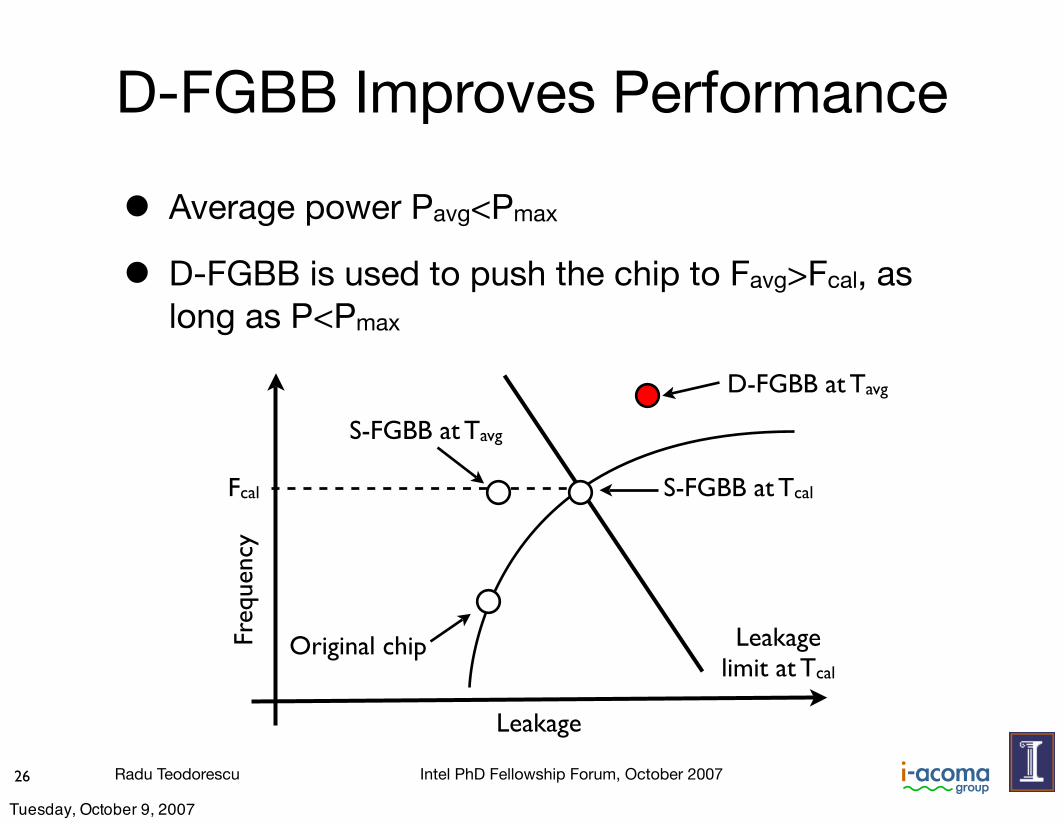
D-FGBB Improves Performance
• Average power Pavg<Pmax
• D-FGBB is used to push the chip to Favg>Fcal, as long as P<Pmax
Freq
uenc
y
Leakage
Leakagelimit at Tcal
Fcal S-FGBB at Tcal
S-FGBB at Tavg
D-FGBB at Tavg
Original chip
Tuesday, October 9, 2007

Radu Teodorescu Intel PhD Fellowship Forum, October 2007
S-FGBB D-FGBB
Normal Improve chip operating point
Save leakage power
High Performance
Improve chip operating point
Increase average frequency
Low Power Save leakagepower
Save leakagepower
Applications of D-FGBB
27
Operating environments
Tuesday, October 9, 2007

Radu Teodorescu Intel PhD Fellowship Forum, October 200728
Freq
uenc
y
Leakage
Leakagelimit at Tcal
Forig
D-FGBB at Tavg
Original chip
D-FGBB Saves Leakage Power
• The chip runs at its original Forig
• D-FGBB adjusts dynamically to T changes to save power while running at Forig
Tuesday, October 9, 2007

Radu Teodorescu Intel PhD Fellowship Forum, October 2007
Outline
• A Model of Process Variation
• Dynamic Fine-Grain Body Biasing
• Evaluation
• Conclusions
29
Tuesday, October 9, 2007

Radu Teodorescu Intel PhD Fellowship Forum, October 2007
Evaluation Infrastructure
• Statistical package R to generate variation maps for 200 chips
• SESC - cycle accurate microarchitectural simulator - execution time, dynamic power
• Mix of SPECint and SPECfp benchmarks
• HotLeakage, SPICE model - leakage power
• Hotspot - temperature estimation
30
Tuesday, October 9, 2007

Radu Teodorescu Intel PhD Fellowship Forum, October 2007
Evaluation Infrastructure
31
R statistical packageVariation model, BB
HotLeakageBSIM3 SPICE
HotspotCMP
FloorplanSESC
Simulatordynamicpower
leakagepower
T leakage powerunder variation
Frequency, power of each chip, under variation
F
Tuesday, October 9, 2007

Radu Teodorescu Intel PhD Fellowship Forum, October 2007
Evaluation Methodology
• 4-core CMP, based on Alpha 21364
• 45nm technology, 4GHz
• Vth variation: σVth/μVth=0.3-0.12, σsys=σrand
• Leff variation σLeff= σVth/2
• Vdd=1V, Vth0=150mV, Vbb= ±500mV
32
Tuesday, October 9, 2007

Radu Teodorescu Intel PhD Fellowship Forum, October 2007
CMP Architecture
33
(c) FGBB64
L2 Cache
DCache
BpredFPRegFPAddFPMul
DTBITBLdSTQIntExec
IntRegFPMapIntMap IntQFPQ
(a) CMP with a detailed processor (b) FGBB16 (d) FGBB144ICache
Figure 9. CMP floor-plan used (a) and the partitioning of one processor and its share of the bus into BB cells (b–d). Chart (b) showsthe five critical path replicas in one cell.
stantially reduces the power consumed at Fcal. Specifically, afterthe manufacturer has set the BB voltages for each cell at Fcal, heproceeds as follows. The supply voltage is reduced in small steps.At each step, our D-FGBB circuit of Figure 6 recomputes the BBvalues, and the total power in the chip is also measured. Whenthe voltage drops so much that Fcal can barely be met, the processstops. Then, we select the combination of supply voltage and BBvalues that consumes the least power. If the processor has multipleDVS domains (e.g., one for the core and one for the L2), this al-gorithm is first run reducing the voltage of one domain only. Oncethe best configuration is found, the configuration is used to run thealgorithm reducing the voltage of another domain, and so on.
5. Selecting the BB CellsMicroarchitectural structure plays an important role in deciding
how to partition the chip into BB cells. There are advantages tousing BB cells with shapes that follow the contour of microarchi-tectural modules such as caches, registers, or execution units. Wesuggest two main reasons for this, namely variations in T and dif-ferences in the types of critical paths in different modules.5.1. Temperature EffectsEquations (1) and (2) show that T significantly affects transistor
leakage and gate delay. At high T, transistors become vastly leakierand gates slower. As a result, the BB voltage applied can be bettertargeted if T does not vary much within a cell. It is well knownthat the spatial T profile in a chip under load follows the layout ofmicroarchitectural modules. For example, the execution unit is hotwhile the L2 cache is cold. Consequently, we propose organizingthe chip into cells that follow the contours of groups of hot andgroups of cold microarchitectural modules.
5.2. Critical Paths in Logic and MemoriesDifferent microarchitectural modules have different types of
critical paths. This is most obvious when comparing logic blockssuch as functional units to memory structures such as the L1 cacheor TLB. In the former, a critical path contains many, physicallyclose gates and a modest amount of wire — e.g., 8-16 FO4-equivalent gates in high-end processors connected by short wires.In contrast, the critical path in memory structures has a few, physi-cally separated transistors and much more wire — e.g., the path thatstretches from a driver through a word line, a pass transistor, a bitline, and then to a sense amplifier.From a Vth variation point of view, these two critical paths differ
dramatically. The transistors in a logic path are many and physi-
cally close. Their large number enables a better averaging of ran-dom Vth variations, while physical proximity makes them subjectto the same systematic Vth variation. On the other hand, the transis-tors in the memory path are few and distant from each other. Fewertransistors means less averaging of random Vth variations, whilefarther distances implies better averaging of systematic Vth varia-tions. Since these two types of critical paths are affected differentlyby a given BB voltage, we separate logic and memory structuresinto different BB cells.
6. Evaluation Methodology6.1. Processor Chip ArchitectureWe use detailed simulations using the SESC [34] cycle-accurate
simulator to evaluate a chip multiprocessor (CMP) with four high-performance processors at 45nm. The processor is based on theAlpha 21364, and has a 64KB L1 I-cache, a 64KB L1 D-cache, anda 2MB L2 cache. We estimate a nominal frequency of 4GHz witha supply voltage of 1V. We generate the processor layout from theAlpha 21364 chip floor-plan, without the router and I/O pads, andwith an L2 cache as in [37]. We use constant scaling to scale thedimensions to 45nm. Finally, we put four such units on a chip, andinterconnect them with a wide snoopy bus. The resulting 8MB L2cache is shared by all the cores. The resulting 132 mm2 chip isshown in Figure 9(a).
6.2. Power and Temperature ModelTo estimate power, we scale the results given by popular tools
using technology projections from ITRS [18]. Specifically, we useSESC augmented with dynamic power models from Wattch [4] toestimate dynamic power at a reference technology and frequency.In addition, we use HotLeakage [48] to estimate leakage power atthe same reference technology. Then, we obtain ITRS’s scalingprojections for the per-transistor dynamic power-delay product, andfor the per-transistor static power. With these two factors, given thatwe keep the number of transistors constant as we scale, we estimatethe dynamic and leakage power for the scaled technology and thefrequency relative to the reference values.We use HotSpot [37] to estimate the on-chip T profile. To do
so, we use the iterative approach of Su et al. [40]: the T is esti-mated based on the current total power; the leakage power is esti-mated based on the current T; and the leakage power is added to thedynamic power. This is repeated until convergence. In our exper-iments, the maximum temperatures reached in the chip are in the95-100 oC range.
Tuesday, October 9, 2007

Radu Teodorescu Intel PhD Fellowship Forum, October 2007
Body Bias Cells
34
(c) FGBB64
L2 Cache
DCache
BpredFPRegFPAddFPMul
DTBITBLdSTQIntExec
IntRegFPMapIntMap IntQFPQ
(a) CMP with a detailed processor (b) FGBB16 (d) FGBB144ICache
Figure 9. CMP floor-plan used (a) and the partitioning of one processor and its share of the bus into BB cells (b–d). Chart (b) showsthe five critical path replicas in one cell.
stantially reduces the power consumed at Fcal. Specifically, afterthe manufacturer has set the BB voltages for each cell at Fcal, heproceeds as follows. The supply voltage is reduced in small steps.At each step, our D-FGBB circuit of Figure 6 recomputes the BBvalues, and the total power in the chip is also measured. Whenthe voltage drops so much that Fcal can barely be met, the processstops. Then, we select the combination of supply voltage and BBvalues that consumes the least power. If the processor has multipleDVS domains (e.g., one for the core and one for the L2), this al-gorithm is first run reducing the voltage of one domain only. Oncethe best configuration is found, the configuration is used to run thealgorithm reducing the voltage of another domain, and so on.
5. Selecting the BB CellsMicroarchitectural structure plays an important role in deciding
how to partition the chip into BB cells. There are advantages tousing BB cells with shapes that follow the contour of microarchi-tectural modules such as caches, registers, or execution units. Wesuggest two main reasons for this, namely variations in T and dif-ferences in the types of critical paths in different modules.5.1. Temperature EffectsEquations (1) and (2) show that T significantly affects transistor
leakage and gate delay. At high T, transistors become vastly leakierand gates slower. As a result, the BB voltage applied can be bettertargeted if T does not vary much within a cell. It is well knownthat the spatial T profile in a chip under load follows the layout ofmicroarchitectural modules. For example, the execution unit is hotwhile the L2 cache is cold. Consequently, we propose organizingthe chip into cells that follow the contours of groups of hot andgroups of cold microarchitectural modules.
5.2. Critical Paths in Logic and MemoriesDifferent microarchitectural modules have different types of
critical paths. This is most obvious when comparing logic blockssuch as functional units to memory structures such as the L1 cacheor TLB. In the former, a critical path contains many, physicallyclose gates and a modest amount of wire — e.g., 8-16 FO4-equivalent gates in high-end processors connected by short wires.In contrast, the critical path in memory structures has a few, physi-cally separated transistors and much more wire — e.g., the path thatstretches from a driver through a word line, a pass transistor, a bitline, and then to a sense amplifier.From a Vth variation point of view, these two critical paths differ
dramatically. The transistors in a logic path are many and physi-
cally close. Their large number enables a better averaging of ran-dom Vth variations, while physical proximity makes them subjectto the same systematic Vth variation. On the other hand, the transis-tors in the memory path are few and distant from each other. Fewertransistors means less averaging of random Vth variations, whilefarther distances implies better averaging of systematic Vth varia-tions. Since these two types of critical paths are affected differentlyby a given BB voltage, we separate logic and memory structuresinto different BB cells.
6. Evaluation Methodology6.1. Processor Chip ArchitectureWe use detailed simulations using the SESC [34] cycle-accurate
simulator to evaluate a chip multiprocessor (CMP) with four high-performance processors at 45nm. The processor is based on theAlpha 21364, and has a 64KB L1 I-cache, a 64KB L1 D-cache, anda 2MB L2 cache. We estimate a nominal frequency of 4GHz witha supply voltage of 1V. We generate the processor layout from theAlpha 21364 chip floor-plan, without the router and I/O pads, andwith an L2 cache as in [37]. We use constant scaling to scale thedimensions to 45nm. Finally, we put four such units on a chip, andinterconnect them with a wide snoopy bus. The resulting 8MB L2cache is shared by all the cores. The resulting 132 mm2 chip isshown in Figure 9(a).
6.2. Power and Temperature ModelTo estimate power, we scale the results given by popular tools
using technology projections from ITRS [18]. Specifically, we useSESC augmented with dynamic power models from Wattch [4] toestimate dynamic power at a reference technology and frequency.In addition, we use HotLeakage [48] to estimate leakage power atthe same reference technology. Then, we obtain ITRS’s scalingprojections for the per-transistor dynamic power-delay product, andfor the per-transistor static power. With these two factors, given thatwe keep the number of transistors constant as we scale, we estimatethe dynamic and leakage power for the scaled technology and thefrequency relative to the reference values.We use HotSpot [37] to estimate the on-chip T profile. To do
so, we use the iterative approach of Su et al. [40]: the T is esti-mated based on the current total power; the leakage power is esti-mated based on the current T; and the leakage power is added to thedynamic power. This is repeated until convergence. In our exper-iments, the maximum temperatures reached in the chip are in the95-100 oC range.
• We partition each core into BB cells
• Shapes and sizes follow functional units
FGBB16 FGBB64 FGBB144
Tuesday, October 9, 2007

Radu Teodorescu Intel PhD Fellowship Forum, October 2007
Variation Impact
35
NoBB
(a)
0 0.5 1.0 1.5 2.0 2.5 3.0leakage
0.8120.8500.8870.9250.9621.0001.037
ycneuqerf
0 0.5 1.0 1.5 2.0 2.5 3.0leakage
0.8120.8500.8870.9250.9621.0001.037
S-FGBB1
(b)
0 0.5 1.0 1.5 2.0 2.5 3.0leakage
0.8120.8500.8870.9250.9621.0001.037
S-FGBB16
(c)
0 0.5 1.0 1.5 2.0 2.5 3.0leakage
0.8120.8500.8870.9250.9621.0001.037
S-FGBB64
(d)
0 0.5 1.0 1.5 2.0 2.5 3.0leakage
0.8120.8500.8870.9250.9621.0001.037
S-FGBB144
(e)
Figure 10. Frequency versus leakage power for a batch of 200 chips at Tcal and full load under various schemes.
0.03 0.06 0.09 0.120
0.20.40.60.81.01.2
Freq
uenc
y
(a)
0.03 0.06 0.09 0.120
0.20.40.60.81.01.21.41.61.8
Leak
age P
ower
!=0.1 !=0.2 !=0.5
(b)"/# "/#
Figure 11. Impact of Vth variation on the chip’s frequency (a)and leakage power (b).
“fall” on the hottest region of the chip, the chip is likely to have lowfrequency. On the other hand, if many transistors with very low Vthfall on the hottest area, the chip is likely to have high leakage.We see two main trends. First, across chips in one experiment,
leakage varies more than frequency — since leakage is exponentialwith T, an unfavorable Vth distribution can significantly increaseleakage power. Second, as ! decreases, the average frequency de-creases as well. The reason is that, given a set of high-Vth transis-tors, if they are uniformly spread out in the chip (low !), there is ahigher chance that some will fall on the hottest region of the chip,thus reducing the chip’s frequency.
7.2. Normal Operation: D-FGBB Improves aChip’s Operating Point
S-FGBB can be used to tune the chips in a batch so that they fallinto desirable frequency-leakage bins [45]. The goal is to place eachchip at the highest possible frequency bin where it still meets thepower consumption constraint. In this section, we summarize theimpact of S-FGBB and then show how D-FGBB further improvesa chip’s operating point.The Acceptable Region for a chip [45] is bounded by two con-
ditions: (i) the frequency should be higher than a given minimumvalue, and (ii) the sum of dynamic and leakage power should beless than a given maximum value. In a frequency-leakage plot suchas Figure 10(a), these constraints require that the chip be above ahorizontal line and to the left of a slanted line, respectively. Theslanted line has this shape because, as frequency increases, the dy-namic power increases linearly and, therefore, the amount of tolera-ble leakage power decreases linearly. Inside the Acceptable Region,higher frequency is better.Figure 10(a) shows a scatter plot of the frequency and leak-
age power for our 200 chips, with axes normalized to NoVar (noprocess-induced Vth variation). We build the slanted line so that it
would include the NoVar chip, which is point (1,1). We then arbi-trarily set the horizontal line to 0.85 of the frequency of the NoVarchip, and divide the range into four equally-spaced frequency bins.As a fraction of the NoVar frequency, the ranges of the bins are:0.850–0.887, 0.887–0.925, 0.925–0.962, and over 0.962. Thesebins are in the ballpark of those used in commercial processors.7.2.1. Impact of S-FGBBIn Figure 10(a), some chips fall outside the Acceptable Region.
By applying S-FGBB to a chip, we can move it into the Accept-able Region or, if it is already there, move it to a higher frequencypoint. Using the axes and the slanted line of Figure 10, Figure 12graphically shows the impact of our S-FGBB calibration algorithmof Section 4.2.
at Tavg
at Tcalat Tcal
calS!FGBB at T
Fcal
Leakage Power
CA’
A
BD!FGBB
D
Freq
uenc
yLeakage limit Original chip
S!FGBB
Figure 12. Impact of S-FGBB and D-FGBB on a chip’soperating point.
Consider a chip that is originally operating at point A. Our al-gorithm can move the chip along the curve labeled S-FGBB atTcal. The result of the algorithm is to bring the chip to point B,at frequency Fcal, where the chip dissipates the maximum allowedpower — thus, point B is on the slanted line. Point B is more desir-able than A in that it is inside the Acceptable Region and is poten-tially in a higher frequency bin than A. Increasing the frequency be-yond Fcal would push the chip to the left of the slanted line, wherepower consumption is excessive. In cases where the original chip isoperating at point A’, the S-FGBB algorithm reduces the frequencyand brings it to point B.The actual curve followed from A depends on the number of
FGBB cells. The schemes with more cells such as FGBB144 targettheir BB voltages better and push the chip to a B position that ishigher in the slanted line — thus delivering chips in better bins.To show it, we take the batch of chips of Figure 10(a) and apply
our S-FGBB algorithm using the FGBB1, FGBB16, FGBB64, andFGBB144 schemes. The resulting frequency-leakage scatter plotsare shown in Figures 10(b)-(e). The charts show that all the schemes
Vth Vth
Tuesday, October 9, 2007

Radu Teodorescu Intel PhD Fellowship Forum, October 2007
S-FGBB D-FGBB
Normal Improve chip operating point
Save leakage power
High Performance
Improve chip operating point
Increase average frequency
Low Power Save leakagepower
Save leakagepower
Applications of D-FGBB
36
Operating environments
Tuesday, October 9, 2007
Radu Teodorescu Intel PhD Fellowship Forum, October 2007
S-FGBB Improves the Chip’s Operating Point
37
NoBB
(a)
0 0.5 1.0 1.5 2.0 2.5 3.0leakage
0.8120.8500.8870.9250.9621.0001.037
ycneuqerf
0 0.5 1.0 1.5 2.0 2.5 3.0leakage
0.8120.8500.8870.9250.9621.0001.037
S-FGBB1
(b)
0 0.5 1.0 1.5 2.0 2.5 3.0leakage
0.8120.8500.8870.9250.9621.0001.037
S-FGBB16
(c)
0 0.5 1.0 1.5 2.0 2.5 3.0leakage
0.8120.8500.8870.9250.9621.0001.037
S-FGBB64
(d)
0 0.5 1.0 1.5 2.0 2.5 3.0leakage
0.8120.8500.8870.9250.9621.0001.037
S-FGBB144
(e)
Figure 10. Frequency versus leakage power for a batch of 200 chips at Tcal and full load under various schemes.
0.03 0.06 0.09 0.120
0.20.40.60.81.01.2
Freq
uenc
y
(a)
0.03 0.06 0.09 0.120
0.20.40.60.81.01.21.41.61.8
Leak
age P
ower
!=0.1 !=0.2 !=0.5
(b)"/# "/#
Figure 11. Impact of Vth variation on the chip’s frequency (a)and leakage power (b).
“fall” on the hottest region of the chip, the chip is likely to have lowfrequency. On the other hand, if many transistors with very low Vthfall on the hottest area, the chip is likely to have high leakage.We see two main trends. First, across chips in one experiment,
leakage varies more than frequency — since leakage is exponentialwith T, an unfavorable Vth distribution can significantly increaseleakage power. Second, as ! decreases, the average frequency de-creases as well. The reason is that, given a set of high-Vth transis-tors, if they are uniformly spread out in the chip (low !), there is ahigher chance that some will fall on the hottest region of the chip,thus reducing the chip’s frequency.
7.2. Normal Operation: D-FGBB Improves aChip’s Operating Point
S-FGBB can be used to tune the chips in a batch so that they fallinto desirable frequency-leakage bins [45]. The goal is to place eachchip at the highest possible frequency bin where it still meets thepower consumption constraint. In this section, we summarize theimpact of S-FGBB and then show how D-FGBB further improvesa chip’s operating point.The Acceptable Region for a chip [45] is bounded by two con-
ditions: (i) the frequency should be higher than a given minimumvalue, and (ii) the sum of dynamic and leakage power should beless than a given maximum value. In a frequency-leakage plot suchas Figure 10(a), these constraints require that the chip be above ahorizontal line and to the left of a slanted line, respectively. Theslanted line has this shape because, as frequency increases, the dy-namic power increases linearly and, therefore, the amount of tolera-ble leakage power decreases linearly. Inside the Acceptable Region,higher frequency is better.Figure 10(a) shows a scatter plot of the frequency and leak-
age power for our 200 chips, with axes normalized to NoVar (noprocess-induced Vth variation). We build the slanted line so that it
would include the NoVar chip, which is point (1,1). We then arbi-trarily set the horizontal line to 0.85 of the frequency of the NoVarchip, and divide the range into four equally-spaced frequency bins.As a fraction of the NoVar frequency, the ranges of the bins are:0.850–0.887, 0.887–0.925, 0.925–0.962, and over 0.962. Thesebins are in the ballpark of those used in commercial processors.7.2.1. Impact of S-FGBBIn Figure 10(a), some chips fall outside the Acceptable Region.
By applying S-FGBB to a chip, we can move it into the Accept-able Region or, if it is already there, move it to a higher frequencypoint. Using the axes and the slanted line of Figure 10, Figure 12graphically shows the impact of our S-FGBB calibration algorithmof Section 4.2.
at Tavg
at Tcalat Tcal
calS!FGBB at T
Fcal
Leakage Power
CA’
A
BD!FGBB
D
Freq
uenc
y
Leakage limit Original chip
S!FGBB
Figure 12. Impact of S-FGBB and D-FGBB on a chip’soperating point.
Consider a chip that is originally operating at point A. Our al-gorithm can move the chip along the curve labeled S-FGBB atTcal. The result of the algorithm is to bring the chip to point B,at frequency Fcal, where the chip dissipates the maximum allowedpower — thus, point B is on the slanted line. Point B is more desir-able than A in that it is inside the Acceptable Region and is poten-tially in a higher frequency bin than A. Increasing the frequency be-yond Fcal would push the chip to the left of the slanted line, wherepower consumption is excessive. In cases where the original chip isoperating at point A’, the S-FGBB algorithm reduces the frequencyand brings it to point B.The actual curve followed from A depends on the number of
FGBB cells. The schemes with more cells such as FGBB144 targettheir BB voltages better and push the chip to a B position that ishigher in the slanted line — thus delivering chips in better bins.To show it, we take the batch of chips of Figure 10(a) and apply
our S-FGBB algorithm using the FGBB1, FGBB16, FGBB64, andFGBB144 schemes. The resulting frequency-leakage scatter plotsare shown in Figures 10(b)-(e). The charts show that all the schemes
0%
11%
28%
55%
36%
57%
Tuesday, October 9, 2007
Radu Teodorescu Intel PhD Fellowship Forum, October 200738
D-FGBB Reduces Leakagemove practically all the chips to the slanted line, in the AcceptableRegion. However, the schemes differ in how high they push thechips. The more BB cells they use, the more effective they are.The different impact of the schemes is best seen in Figure 13,
which shows how many chips fall in each frequency bin for the dif-ferent schemes as a fraction of the 200 chips. Chart (a) correspondsto our experiment, while (b) repeats it for Vth’s !/µ = 0.09.
0.850-0.8870.887-0.925
0.925-0.962over 0.962
Frequency Bin
010.020.030.040.050.060.070.080.0
Chip
coun
t (%
)
NoBB S-FGBB1 S-FGBB16 S-FGBB64 S-FGBB144
(a)
0.850-0.8870.887-0.925
0.925-0.962over 0.962
Frequency Bin
010.020.030.040.050.060.070.080.0
Chip
coun
t (%
)
(b)Figure 13. Frequency binning obtained by S-FGBB with differ-ent numbers of BB cells, for !/µ = 0.12 (a) and !/µ = 0.09(b).Figure 13(a) shows that FGBB64 and FGBB144 move many
chips to the top bin. Specifically, FGBB144 has 36% of the chips inthe top bin and 93% in the top two. On the other hand, NoBB hasnone in the top bin and only 11% in the top two. Chart (b) showsthat the trends are the same for !/µ = 0.09. Specifically, as wego from NoBB to FGBB144, the number of chips in the top binchanges from 4% to 75%. Consequently, our results are valid forsmaller variations as well.In the rest of the paper, when we refer to the average frequency
and leakage of the NoBB or other schemes, we count all the chips— rather than dropping from the average those that fall outside theAcceptable Region. While in a practical environment they wouldbe dropped, we feel the results are more intuitive this way.7.2.2. Leakage Reduction with D-FGBBApplying the D-FGBB algorithm of Section 4.3 can substan-
tially reduce the leakage power consumed by the chip. To see itgraphically, consider Figure 12. The chip was calibrated with S-FGBB at Tcal, resulting in point B. However, given that the chip’s Tduring execution is close to Tavg , the chip typically operates aroundpoint C, moving to the left and right as shown depending on the cur-rent T conditions. If we apply D-FGBB, we push the chip’s workingpoint to moving around point D in the figure. The result is leakagepower savings.Figure 14(a) compares the leakage power of the chips under
NoBB, and with 1, 16, 64, or 144 cells under S-FGBB and D-FGBB. We report the average across all the applications and nor-malize the bars to NoBB. We see that D-FGBB reduces the leakagesubstantially over S-FGBB. Specifically, with D-FGBB, the leak-age power is reduced by 28–42% compared to S-FGBB — wherethe highest reductions correspond to the chips with more cells. In allcases, S-FGBB dissipates about the same amount of leakage poweras NoBB.Figure 14(b) shows the total power in this experiment. The fig-
ure also includes an environment with DVS alone and one whereD-FGBB is combined with DVS as detailed in Section 4.5. All bars
1 16 64 144Number of BB Cells
00.20.40.60.81.0
Leak
age P
ower
NoBBS-FGBBD-FGBB
(a)
1 16 64 144Number of BB Cells
00.20.40.60.81.0
Total
Pow
er
NoBBDVSS-FGBB
D-FGBBD-FGBB+DVS
(b)Figure 14. Leakage (a) and total power (b) of the chips fordifferent FGBB schemes in normal operation.
are normalized to NoBB. Recall that, as we increase the number ofcells, the frequency increases. However, for the same number ofcells, the frequency is the same. From the figure, we see that D-FGBB reduces the total power consumption by 15–22% relative toS-FGBB for the same frequency, with the higher reductions corre-sponding to the schemes with more cells. If we combine D-FGBBand DVS, the total power saved is 21–36% of the S-FGBB power—again, with the schemes with more cells doing the best. This largeimpact is possible because DVS lowers the voltage of the domainthat dissipates the most dynamic power (namely, the core), whileD-FGBB applies higher BB to ensure that the target frequency ismet. This results in dynamic power savings that add to the leak-age savings of D-FGBB. Finally, DVS alone can only reduce lessthan 5% of the power in NoBB. This is because the voltage can belowered little while still meeting the target frequency.
7.3. High Performance: D-FGBB Improves Fre-quency
A second application of D-FGBB is to improve performance byincreasing the average frequency of a chip beyond the Fcal deter-mined at calibration (Section 4.4). Figure 15 compares the averagefrequency of the chips with S-FGBB and this use of D-FGBB. Thefigure considers chips with different numbers of cells, and normal-izes the bars to NoBB.We see that D-FGBB increases the frequencyby 7–9% over S-FGBB for the same number of cells. Compared toNoBB, the frequency increase is 7–16%. With more cells, the fre-quency is higher because BB can be tuned better.
1 16 64 1440.50.60.70.80.91.01.11.2
Freq
uenc
y
NoBBS-FGBBD-FGBB
Figure 15. Average frequency of the chips for different FGBBschemes.
The frequency increase varies across applications, depending ontheir dynamic power consumption. Those with low dynamic powerconsumption see the biggest boosts in frequency. However, appli-cations benefit differently from a frequency boost, depending onwhether they are memory- or compute-intensive. Figure 17 com-pares the execution time of the applications with S-FGBB144 and
move practically all the chips to the slanted line, in the AcceptableRegion. However, the schemes differ in how high they push thechips. The more BB cells they use, the more effective they are.The different impact of the schemes is best seen in Figure 13,
which shows how many chips fall in each frequency bin for the dif-ferent schemes as a fraction of the 200 chips. Chart (a) correspondsto our experiment, while (b) repeats it for Vth’s !/µ = 0.09.
0.850-0.8870.887-0.925
0.925-0.962over 0.962
Frequency Bin
010.020.030.040.050.060.070.080.0
Chip
coun
t (%
)
NoBB S-FGBB1 S-FGBB16 S-FGBB64 S-FGBB144
(a)
0.850-0.8870.887-0.925
0.925-0.962over 0.962
Frequency Bin
010.020.030.040.050.060.070.080.0
Chip
coun
t (%
)
(b)Figure 13. Frequency binning obtained by S-FGBB with differ-ent numbers of BB cells, for !/µ = 0.12 (a) and !/µ = 0.09(b).Figure 13(a) shows that FGBB64 and FGBB144 move many
chips to the top bin. Specifically, FGBB144 has 36% of the chips inthe top bin and 93% in the top two. On the other hand, NoBB hasnone in the top bin and only 11% in the top two. Chart (b) showsthat the trends are the same for !/µ = 0.09. Specifically, as wego from NoBB to FGBB144, the number of chips in the top binchanges from 4% to 75%. Consequently, our results are valid forsmaller variations as well.In the rest of the paper, when we refer to the average frequency
and leakage of the NoBB or other schemes, we count all the chips— rather than dropping from the average those that fall outside theAcceptable Region. While in a practical environment they wouldbe dropped, we feel the results are more intuitive this way.7.2.2. Leakage Reduction with D-FGBBApplying the D-FGBB algorithm of Section 4.3 can substan-
tially reduce the leakage power consumed by the chip. To see itgraphically, consider Figure 12. The chip was calibrated with S-FGBB at Tcal, resulting in point B. However, given that the chip’s Tduring execution is close to Tavg , the chip typically operates aroundpoint C, moving to the left and right as shown depending on the cur-rent T conditions. If we apply D-FGBB, we push the chip’s workingpoint to moving around point D in the figure. The result is leakagepower savings.Figure 14(a) compares the leakage power of the chips under
NoBB, and with 1, 16, 64, or 144 cells under S-FGBB and D-FGBB. We report the average across all the applications and nor-malize the bars to NoBB. We see that D-FGBB reduces the leakagesubstantially over S-FGBB. Specifically, with D-FGBB, the leak-age power is reduced by 28–42% compared to S-FGBB — wherethe highest reductions correspond to the chips with more cells. In allcases, S-FGBB dissipates about the same amount of leakage poweras NoBB.Figure 14(b) shows the total power in this experiment. The fig-
ure also includes an environment with DVS alone and one whereD-FGBB is combined with DVS as detailed in Section 4.5. All bars
1 16 64 144Number of BB Cells
00.20.40.60.81.0
Leak
age P
ower
NoBBS-FGBBD-FGBB
(a)
1 16 64 144Number of BB Cells
00.20.40.60.81.0
Total
Pow
er
NoBBDVSS-FGBB
D-FGBBD-FGBB+DVS
(b)Figure 14. Leakage (a) and total power (b) of the chips fordifferent FGBB schemes in normal operation.
are normalized to NoBB. Recall that, as we increase the number ofcells, the frequency increases. However, for the same number ofcells, the frequency is the same. From the figure, we see that D-FGBB reduces the total power consumption by 15–22% relative toS-FGBB for the same frequency, with the higher reductions corre-sponding to the schemes with more cells. If we combine D-FGBBand DVS, the total power saved is 21–36% of the S-FGBB power—again, with the schemes with more cells doing the best. This largeimpact is possible because DVS lowers the voltage of the domainthat dissipates the most dynamic power (namely, the core), whileD-FGBB applies higher BB to ensure that the target frequency ismet. This results in dynamic power savings that add to the leak-age savings of D-FGBB. Finally, DVS alone can only reduce lessthan 5% of the power in NoBB. This is because the voltage can belowered little while still meeting the target frequency.
7.3. High Performance: D-FGBB Improves Fre-quency
A second application of D-FGBB is to improve performance byincreasing the average frequency of a chip beyond the Fcal deter-mined at calibration (Section 4.4). Figure 15 compares the averagefrequency of the chips with S-FGBB and this use of D-FGBB. Thefigure considers chips with different numbers of cells, and normal-izes the bars to NoBB.We see that D-FGBB increases the frequencyby 7–9% over S-FGBB for the same number of cells. Compared toNoBB, the frequency increase is 7–16%. With more cells, the fre-quency is higher because BB can be tuned better.
1 16 64 1440.50.60.70.80.91.01.11.2
Freq
uenc
y
NoBBS-FGBBD-FGBB
Figure 15. Average frequency of the chips for different FGBBschemes.
The frequency increase varies across applications, depending ontheir dynamic power consumption. Those with low dynamic powerconsumption see the biggest boosts in frequency. However, appli-cations benefit differently from a frequency boost, depending onwhether they are memory- or compute-intensive. Figure 17 com-pares the execution time of the applications with S-FGBB144 and
• Large leakage reduction after binning: 28-42%
• More BB cells result in higher savings
Tuesday, October 9, 2007

Radu Teodorescu Intel PhD Fellowship Forum, October 2007
S-FGBB D-FGBB
Normal Improve chip operating point
Save leakage power
High Performance
Improve chip operating point
Increase average frequency
Low Power Save leakagepower
Save leakagepower
Applications of D-FGBB
39
Operating environments
Tuesday, October 9, 2007

Radu Teodorescu Intel PhD Fellowship Forum, October 2007
D-FGBB Improves Frequency
40
move practically all the chips to the slanted line, in the AcceptableRegion. However, the schemes differ in how high they push thechips. The more BB cells they use, the more effective they are.The different impact of the schemes is best seen in Figure 13,
which shows how many chips fall in each frequency bin for the dif-ferent schemes as a fraction of the 200 chips. Chart (a) correspondsto our experiment, while (b) repeats it for Vth’s σ/µ = 0.09.
0.850-0.8870.887-0.925
0.925-0.962over 0.962
Frequency Bin
010.020.030.040.050.060.070.080.0
Chip
coun
t (%
)
NoBB S-FGBB1 S-FGBB16 S-FGBB64 S-FGBB144
(a)
0.850-0.8870.887-0.925
0.925-0.962over 0.962
Frequency Bin
010.020.030.040.050.060.070.080.0
Chip
coun
t (%
)
(b)Figure 13. Frequency binning obtained by S-FGBB with differ-ent numbers of BB cells, for σ/µ = 0.12 (a) and σ/µ = 0.09(b).Figure 13(a) shows that FGBB64 and FGBB144 move many
chips to the top bin. Specifically, FGBB144 has 36% of the chips inthe top bin and 93% in the top two. On the other hand, NoBB hasnone in the top bin and only 11% in the top two. Chart (b) showsthat the trends are the same for σ/µ = 0.09. Specifically, as wego from NoBB to FGBB144, the number of chips in the top binchanges from 4% to 75%. Consequently, our results are valid forsmaller variations as well.In the rest of the paper, when we refer to the average frequency
and leakage of the NoBB or other schemes, we count all the chips— rather than dropping from the average those that fall outside theAcceptable Region. While in a practical environment they wouldbe dropped, we feel the results are more intuitive this way.7.2.2. Leakage Reduction with D-FGBBApplying the D-FGBB algorithm of Section 4.3 can substan-
tially reduce the leakage power consumed by the chip. To see itgraphically, consider Figure 12. The chip was calibrated with S-FGBB at Tcal, resulting in point B. However, given that the chip’s Tduring execution is close to Tavg , the chip typically operates aroundpoint C, moving to the left and right as shown depending on the cur-rent T conditions. If we apply D-FGBB, we push the chip’s workingpoint to moving around point D in the figure. The result is leakagepower savings.Figure 14(a) compares the leakage power of the chips under
NoBB, and with 1, 16, 64, or 144 cells under S-FGBB and D-FGBB. We report the average across all the applications and nor-malize the bars to NoBB. We see that D-FGBB reduces the leakagesubstantially over S-FGBB. Specifically, with D-FGBB, the leak-age power is reduced by 28–42% compared to S-FGBB — wherethe highest reductions correspond to the chips with more cells. In allcases, S-FGBB dissipates about the same amount of leakage poweras NoBB.Figure 14(b) shows the total power in this experiment. The fig-
ure also includes an environment with DVS alone and one whereD-FGBB is combined with DVS as detailed in Section 4.5. All bars
1 16 64 144Number of BB Cells
00.20.40.60.81.0
Leak
age P
ower
NoBBS-FGBBD-FGBB
(a)
1 16 64 144Number of BB Cells
00.20.40.60.81.0
Total
Pow
er
NoBBDVSS-FGBB
D-FGBBD-FGBB+DVS
(b)Figure 14. Leakage (a) and total power (b) of the chips fordifferent FGBB schemes in normal operation.
are normalized to NoBB. Recall that, as we increase the number ofcells, the frequency increases. However, for the same number ofcells, the frequency is the same. From the figure, we see that D-FGBB reduces the total power consumption by 15–22% relative toS-FGBB for the same frequency, with the higher reductions corre-sponding to the schemes with more cells. If we combine D-FGBBand DVS, the total power saved is 21–36% of the S-FGBB power—again, with the schemes with more cells doing the best. This largeimpact is possible because DVS lowers the voltage of the domainthat dissipates the most dynamic power (namely, the core), whileD-FGBB applies higher BB to ensure that the target frequency ismet. This results in dynamic power savings that add to the leak-age savings of D-FGBB. Finally, DVS alone can only reduce lessthan 5% of the power in NoBB. This is because the voltage can belowered little while still meeting the target frequency.
7.3. High Performance: D-FGBB Improves Fre-quency
A second application of D-FGBB is to improve performance byincreasing the average frequency of a chip beyond the Fcal deter-mined at calibration (Section 4.4). Figure 15 compares the averagefrequency of the chips with S-FGBB and this use of D-FGBB. Thefigure considers chips with different numbers of cells, and normal-izes the bars to NoBB.We see that D-FGBB increases the frequencyby 7–9% over S-FGBB for the same number of cells. Compared toNoBB, the frequency increase is 7–16%. With more cells, the fre-quency is higher because BB can be tuned better.
1 16 64 1440.50.60.70.80.91.01.11.2
Freq
uenc
y
NoBBS-FGBBD-FGBB
Figure 15. Average frequency of the chips for different FGBBschemes.
The frequency increase varies across applications, depending ontheir dynamic power consumption. Those with low dynamic powerconsumption see the biggest boosts in frequency. However, appli-cations benefit differently from a frequency boost, depending onwhether they are memory- or compute-intensive. Figure 17 com-pares the execution time of the applications with S-FGBB144 and
move practically all the chips to the slanted line, in the AcceptableRegion. However, the schemes differ in how high they push thechips. The more BB cells they use, the more effective they are.The different impact of the schemes is best seen in Figure 13,
which shows how many chips fall in each frequency bin for the dif-ferent schemes as a fraction of the 200 chips. Chart (a) correspondsto our experiment, while (b) repeats it for Vth’s !/µ = 0.09.
0.850-0.8870.887-0.925
0.925-0.962over 0.962
Frequency Bin
010.020.030.040.050.060.070.080.0
Chip
coun
t (%
)
NoBB S-FGBB1 S-FGBB16 S-FGBB64 S-FGBB144
(a)
0.850-0.8870.887-0.925
0.925-0.962over 0.962
Frequency Bin
010.020.030.040.050.060.070.080.0
Chip
coun
t (%
)
(b)Figure 13. Frequency binning obtained by S-FGBB with differ-ent numbers of BB cells, for !/µ = 0.12 (a) and !/µ = 0.09(b).Figure 13(a) shows that FGBB64 and FGBB144 move many
chips to the top bin. Specifically, FGBB144 has 36% of the chips inthe top bin and 93% in the top two. On the other hand, NoBB hasnone in the top bin and only 11% in the top two. Chart (b) showsthat the trends are the same for !/µ = 0.09. Specifically, as wego from NoBB to FGBB144, the number of chips in the top binchanges from 4% to 75%. Consequently, our results are valid forsmaller variations as well.In the rest of the paper, when we refer to the average frequency
and leakage of the NoBB or other schemes, we count all the chips— rather than dropping from the average those that fall outside theAcceptable Region. While in a practical environment they wouldbe dropped, we feel the results are more intuitive this way.7.2.2. Leakage Reduction with D-FGBBApplying the D-FGBB algorithm of Section 4.3 can substan-
tially reduce the leakage power consumed by the chip. To see itgraphically, consider Figure 12. The chip was calibrated with S-FGBB at Tcal, resulting in point B. However, given that the chip’s Tduring execution is close to Tavg , the chip typically operates aroundpoint C, moving to the left and right as shown depending on the cur-rent T conditions. If we apply D-FGBB, we push the chip’s workingpoint to moving around point D in the figure. The result is leakagepower savings.Figure 14(a) compares the leakage power of the chips under
NoBB, and with 1, 16, 64, or 144 cells under S-FGBB and D-FGBB. We report the average across all the applications and nor-malize the bars to NoBB. We see that D-FGBB reduces the leakagesubstantially over S-FGBB. Specifically, with D-FGBB, the leak-age power is reduced by 28–42% compared to S-FGBB — wherethe highest reductions correspond to the chips with more cells. In allcases, S-FGBB dissipates about the same amount of leakage poweras NoBB.Figure 14(b) shows the total power in this experiment. The fig-
ure also includes an environment with DVS alone and one whereD-FGBB is combined with DVS as detailed in Section 4.5. All bars
1 16 64 144Number of BB Cells
00.20.40.60.81.0
Leak
age P
ower
NoBBS-FGBBD-FGBB
(a)
1 16 64 144Number of BB Cells
00.20.40.60.81.0
Total
Pow
er
NoBBDVSS-FGBB
D-FGBBD-FGBB+DVS
(b)Figure 14. Leakage (a) and total power (b) of the chips fordifferent FGBB schemes in normal operation.
are normalized to NoBB. Recall that, as we increase the number ofcells, the frequency increases. However, for the same number ofcells, the frequency is the same. From the figure, we see that D-FGBB reduces the total power consumption by 15–22% relative toS-FGBB for the same frequency, with the higher reductions corre-sponding to the schemes with more cells. If we combine D-FGBBand DVS, the total power saved is 21–36% of the S-FGBB power—again, with the schemes with more cells doing the best. This largeimpact is possible because DVS lowers the voltage of the domainthat dissipates the most dynamic power (namely, the core), whileD-FGBB applies higher BB to ensure that the target frequency ismet. This results in dynamic power savings that add to the leak-age savings of D-FGBB. Finally, DVS alone can only reduce lessthan 5% of the power in NoBB. This is because the voltage can belowered little while still meeting the target frequency.
7.3. High Performance: D-FGBB Improves Fre-quency
A second application of D-FGBB is to improve performance byincreasing the average frequency of a chip beyond the Fcal deter-mined at calibration (Section 4.4). Figure 15 compares the averagefrequency of the chips with S-FGBB and this use of D-FGBB. Thefigure considers chips with different numbers of cells, and normal-izes the bars to NoBB.We see that D-FGBB increases the frequencyby 7–9% over S-FGBB for the same number of cells. Compared toNoBB, the frequency increase is 7–16%. With more cells, the fre-quency is higher because BB can be tuned better.
1 16 64 1440.50.60.70.80.91.01.11.2
Freq
uenc
y
NoBBS-FGBBD-FGBB
Figure 15. Average frequency of the chips for different FGBBschemes.
The frequency increase varies across applications, depending ontheir dynamic power consumption. Those with low dynamic powerconsumption see the biggest boosts in frequency. However, appli-cations benefit differently from a frequency boost, depending onwhether they are memory- or compute-intensive. Figure 17 com-pares the execution time of the applications with S-FGBB144 and
• Average frequency improvement 7-9% over S-FGBB and 7-16% over NoBB
• More BB cells result in higher increase
Tuesday, October 9, 2007

Radu Teodorescu Intel PhD Fellowship Forum, October 200741
Power Cost
0 0.5 1.0leakage
0.8120.8500.8870.9250.9621.0001.037
frequ
ency
NoBB
(a)
0 0.5 1.0leakage
0.8120.8500.8870.9250.9621.0001.037
S-FGBB64
(b)
0 0.5 1.0leakage
0.8120.8500.8870.9250.9621.0001.037
S-FGBB144
(c)
0 0.5 1.0leakage
0.8120.8500.8870.9250.9621.0001.037
D-FGBB64
(d)
0 0.5 1.0leakage
0.8120.8500.8870.9250.9621.0001.037
D-FGBB144
(e)
Figure 16. Frequency versus leakage power for a batch of 200 chips at usual T and load conditions.
D-FGBB144. In the figure, the bars are normalized to NoBB.On average, D-FGBB144 reduces the execution time by 6% overS-FGBB144. Moreover, compared to NoBB and S-FGBB1 (notshown in the figure), the reduction is 10%.
applu
bzip2
crafty
equa
ke gap
gzip mcf
mesa
mgrid
parse
rsw
imtw
olfA.m
ean
0.50.60.70.80.91.0
Exec
ution
Tim
e
NoBB S-FGBB144 D-FGBB144
Figure 17. Execution time of the applications for different FGBBschemes.
The speedups delivered by D-FGBB come at a significant cost intotal power consumption. Increasing the frequency induces higherdynamic power; applying the more aggressive BB voltage neededto increase frequency induces higher leakage power. The result-ing total power for S-FGBB and D-FGBB is shown in Figure 18.Because of the high power cost, this mode of operation is only ap-pealing when the highest possible performance is needed.
1 16 64 144Number of BB Cells
00.20.40.60.81.0
Total
Pow
er
NoBBS-FGBBD-FGBB
Figure 18. Total power of the chips for different FGBB schemes.
7.4. Low Power: D-FGBB Reduces LeakageFinally, we consider an environment where we do not attempt to
improve the original frequency of the chip with the S-FGBB cali-bration step of Section 4.2. Instead, we take each chip in the batchin turn, identify the frequency at which it runs, and then apply D-FGBB (or S-FGBB) to save leakage. Our goal is to save as muchleakage as possible. We call this environment low power mode.
7.4.1. Constant FrequencyFirst, we look at the case when the frequency of the chip does
not change. The result is shown in Figure 16. In Figure 16(a), werepeat the frequency-leakage scatter plot of Figure 10(a), this timeat usual T and load conditions. As a result, the leakage power issignificantly lower than in the worst case presented in Figure 10(a).Then, Figures 16(b)-(e) show the result of applying S-FGBB or D-FGBB with different numbers of cells, to reduce leakage at constantfrequency.Comparing Chart (a) to (b)-(c), we see that, if we apply S-
FGBB, the chips move to the left, therefore saving leakage. More-over, Charts (d)-(e) show that D-FGBB reduces the leakage of thechips even further. The higher the number of cells per chip is, thehigher the leakage reduction is.Figure 19 extends these experiments to all the BB environments.
Figure 19(a) shows the average leakage power of the chips normal-ized to NoBB. The figure shows that both S-FGBB and D-FGBBsave substantial leakage, especially as the number of cells per chipincreases. However, D-FGBB is much more effective. D-FGBBreduces the leakage by 10–51% compared to S-FGBB, and by 12–69% compared to NoBB. Even with only 16 cells per chip, D-FGBBsaves substantial leakage.Figure 19(b) shows the total power consumption for the differ-
ent FGBB schemes, DVS, and D-FGBB+DVS. The savings inducedby D-FGBB are still large. Specifically, D-FGBB reduces the to-tal power consumption by 6–19% relative to S-FGBB. When com-bined with DVS, D-FGBB+DVS reduces total power consumptionby 15–36% compared to S-FGBB. DVS alone is not very effective.
1 16 64 144Number of BB Cells
00.20.40.60.81.0
Leak
age P
ower
NoBBS-FGBBD-FGBB
(a)
1 16 64 144Number of BB Cells
00.20.40.60.81.0
Total
Pow
er
NoBBDVSS-FGBB
D-FGBBD-FGBB+DVS
(b)Figure 19. Leakage (a) and total power (b) of the chips fordifferent FGBB schemes at constant frequency.
7.4.2. Dynamic Voltage and Frequency Scaling (DVFS)Since many processors today use DVFS to save power, we
would like to examine how the effectiveness of D-FGBB changes as
Pmax
• Significant power cost, but still within the power budget
Tuesday, October 9, 2007

Radu Teodorescu Intel PhD Fellowship Forum, October 2007
S-FGBB D-FGBB
Normal Improve chip operating point
Save leakage power
High Performance
Improve chip operating point
Increase average frequency
Low Power Save leakagepower
Save leakagepower
Applications of D-FGBB
42
Operating environments
Tuesday, October 9, 2007
Radu Teodorescu Intel PhD Fellowship Forum, October 200743
0 0.5 1.0leakage
0.8120.8500.8870.9250.9621.0001.037
frequ
ency
NoBB
(a)
0 0.5 1.0leakage
0.8120.8500.8870.9250.9621.0001.037
S-FGBB64
(b)
0 0.5 1.0leakage
0.8120.8500.8870.9250.9621.0001.037
S-FGBB144
(c)
0 0.5 1.0leakage
0.8120.8500.8870.9250.9621.0001.037
D-FGBB64
(d)
0 0.5 1.0leakage
0.8120.8500.8870.9250.9621.0001.037
D-FGBB144
(e)
Figure 16. Frequency versus leakage power for a batch of 200 chips at usual T and load conditions.
D-FGBB144. In the figure, the bars are normalized to NoBB.On average, D-FGBB144 reduces the execution time by 6% overS-FGBB144. Moreover, compared to NoBB and S-FGBB1 (notshown in the figure), the reduction is 10%.
applu
bzip2
crafty
equa
ke gap
gzip mcf
mesa
mgrid
parse
rsw
imtw
olfA.m
ean
0.50.60.70.80.91.0
Exec
ution
Tim
e
NoBB S-FGBB144 D-FGBB144
Figure 17. Execution time of the applications for different FGBBschemes.
The speedups delivered by D-FGBB come at a significant cost intotal power consumption. Increasing the frequency induces higherdynamic power; applying the more aggressive BB voltage neededto increase frequency induces higher leakage power. The result-ing total power for S-FGBB and D-FGBB is shown in Figure 18.Because of the high power cost, this mode of operation is only ap-pealing when the highest possible performance is needed.
1 16 64 144Number of BB Cells
00.20.40.60.81.0
Total
Pow
er
NoBBS-FGBBD-FGBB
Figure 18. Total power of the chips for different FGBB schemes.
7.4. Low Power: D-FGBB Reduces LeakageFinally, we consider an environment where we do not attempt to
improve the original frequency of the chip with the S-FGBB cali-bration step of Section 4.2. Instead, we take each chip in the batchin turn, identify the frequency at which it runs, and then apply D-FGBB (or S-FGBB) to save leakage. Our goal is to save as muchleakage as possible. We call this environment low power mode.
7.4.1. Constant FrequencyFirst, we look at the case when the frequency of the chip does
not change. The result is shown in Figure 16. In Figure 16(a), werepeat the frequency-leakage scatter plot of Figure 10(a), this timeat usual T and load conditions. As a result, the leakage power issignificantly lower than in the worst case presented in Figure 10(a).Then, Figures 16(b)-(e) show the result of applying S-FGBB or D-FGBB with different numbers of cells, to reduce leakage at constantfrequency.Comparing Chart (a) to (b)-(c), we see that, if we apply S-
FGBB, the chips move to the left, therefore saving leakage. More-over, Charts (d)-(e) show that D-FGBB reduces the leakage of thechips even further. The higher the number of cells per chip is, thehigher the leakage reduction is.Figure 19 extends these experiments to all the BB environments.
Figure 19(a) shows the average leakage power of the chips normal-ized to NoBB. The figure shows that both S-FGBB and D-FGBBsave substantial leakage, especially as the number of cells per chipincreases. However, D-FGBB is much more effective. D-FGBBreduces the leakage by 10–51% compared to S-FGBB, and by 12–69% compared to NoBB. Even with only 16 cells per chip, D-FGBBsaves substantial leakage.Figure 19(b) shows the total power consumption for the differ-
ent FGBB schemes, DVS, and D-FGBB+DVS. The savings inducedby D-FGBB are still large. Specifically, D-FGBB reduces the to-tal power consumption by 6–19% relative to S-FGBB. When com-bined with DVS, D-FGBB+DVS reduces total power consumptionby 15–36% compared to S-FGBB. DVS alone is not very effective.
1 16 64 144Number of BB Cells
00.20.40.60.81.0
Leak
age P
ower
NoBBS-FGBBD-FGBB
(a)
1 16 64 144Number of BB Cells
00.20.40.60.81.0
Total
Pow
er
NoBBDVSS-FGBB
D-FGBBD-FGBB+DVS
(b)Figure 19. Leakage (a) and total power (b) of the chips fordifferent FGBB schemes at constant frequency.
7.4.2. Dynamic Voltage and Frequency Scaling (DVFS)Since many processors today use DVFS to save power, we
would like to examine how the effectiveness of D-FGBB changes as
0 0.5 1.0leakage
0.8120.8500.8870.9250.9621.0001.037
frequ
ency
NoBB
(a)
0 0.5 1.0leakage
0.8120.8500.8870.9250.9621.0001.037
S-FGBB64
(b)
0 0.5 1.0leakage
0.8120.8500.8870.9250.9621.0001.037
S-FGBB144
(c)
0 0.5 1.0leakage
0.8120.8500.8870.9250.9621.0001.037
D-FGBB64
(d)
0 0.5 1.0leakage
0.8120.8500.8870.9250.9621.0001.037
D-FGBB144
(e)
Figure 16. Frequency versus leakage power for a batch of 200 chips at usual T and load conditions.
D-FGBB144. In the figure, the bars are normalized to NoBB.On average, D-FGBB144 reduces the execution time by 6% overS-FGBB144. Moreover, compared to NoBB and S-FGBB1 (notshown in the figure), the reduction is 10%.
applu
bzip2
crafty
equa
ke gap
gzip mcf
mesa
mgrid
parse
rsw
imtw
olfA.m
ean
0.50.60.70.80.91.0
Exec
ution
Tim
e
NoBB S-FGBB144 D-FGBB144
Figure 17. Execution time of the applications for different FGBBschemes.
The speedups delivered by D-FGBB come at a significant cost intotal power consumption. Increasing the frequency induces higherdynamic power; applying the more aggressive BB voltage neededto increase frequency induces higher leakage power. The result-ing total power for S-FGBB and D-FGBB is shown in Figure 18.Because of the high power cost, this mode of operation is only ap-pealing when the highest possible performance is needed.
1 16 64 144Number of BB Cells
00.20.40.60.81.0
Total
Pow
er
NoBBS-FGBBD-FGBB
Figure 18. Total power of the chips for different FGBB schemes.
7.4. Low Power: D-FGBB Reduces LeakageFinally, we consider an environment where we do not attempt to
improve the original frequency of the chip with the S-FGBB cali-bration step of Section 4.2. Instead, we take each chip in the batchin turn, identify the frequency at which it runs, and then apply D-FGBB (or S-FGBB) to save leakage. Our goal is to save as muchleakage as possible. We call this environment low power mode.
7.4.1. Constant FrequencyFirst, we look at the case when the frequency of the chip does
not change. The result is shown in Figure 16. In Figure 16(a), werepeat the frequency-leakage scatter plot of Figure 10(a), this timeat usual T and load conditions. As a result, the leakage power issignificantly lower than in the worst case presented in Figure 10(a).Then, Figures 16(b)-(e) show the result of applying S-FGBB or D-FGBB with different numbers of cells, to reduce leakage at constantfrequency.Comparing Chart (a) to (b)-(c), we see that, if we apply S-
FGBB, the chips move to the left, therefore saving leakage. More-over, Charts (d)-(e) show that D-FGBB reduces the leakage of thechips even further. The higher the number of cells per chip is, thehigher the leakage reduction is.Figure 19 extends these experiments to all the BB environments.
Figure 19(a) shows the average leakage power of the chips normal-ized to NoBB. The figure shows that both S-FGBB and D-FGBBsave substantial leakage, especially as the number of cells per chipincreases. However, D-FGBB is much more effective. D-FGBBreduces the leakage by 10–51% compared to S-FGBB, and by 12–69% compared to NoBB. Even with only 16 cells per chip, D-FGBBsaves substantial leakage.Figure 19(b) shows the total power consumption for the differ-
ent FGBB schemes, DVS, and D-FGBB+DVS. The savings inducedby D-FGBB are still large. Specifically, D-FGBB reduces the to-tal power consumption by 6–19% relative to S-FGBB. When com-bined with DVS, D-FGBB+DVS reduces total power consumptionby 15–36% compared to S-FGBB. DVS alone is not very effective.
1 16 64 144Number of BB Cells
00.20.40.60.81.0
Leak
age P
ower
NoBBS-FGBBD-FGBB
(a)
1 16 64 144Number of BB Cells
00.20.40.60.81.0
Total
Pow
er
NoBBDVSS-FGBB
D-FGBBD-FGBB+DVS
(b)Figure 19. Leakage (a) and total power (b) of the chips fordifferent FGBB schemes at constant frequency.
7.4.2. Dynamic Voltage and Frequency Scaling (DVFS)Since many processors today use DVFS to save power, we
would like to examine how the effectiveness of D-FGBB changes as
D-FGBB Reduces Leakage
• Large leakage reduction at constant frequency: 10-51% vs. S-FGBB and 12-69% vs NoBB
• More BB cells result in higher savings
Tuesday, October 9, 2007

Radu Teodorescu Intel PhD Fellowship Forum, October 2007
• D-FGBB targets leakage power
• DVFS targets mostly dynamic power
• Can they be combined effectively?
44
Combining D-FGBB with DVFS
Tuesday, October 9, 2007

Radu Teodorescu Intel PhD Fellowship Forum, October 200745
Combining D-FGBB with DVFS
Vdd decreases with DVFS. For that, we take each chip in the batchand, for a set of supply voltages V i
dd ranging from 1V to 0.6V, de-termine the corresponding frequency Fi before BB. Then, we applyD-FGBB at Fi. Finally, we measure the leakage and total powersfor each V i
dd before and after applying D-FGBB. The results areshown in Figure 20, where all bars are normalized to NoBB withVdd=1V.
1 V 0.8 V 0.6 V Vdd
00.20.40.60.81.0
Leak
age P
ower
(a)
1 V 0.8 V 0.6 V Vdd
00.20.40.60.81.0
Total
Pow
er
NoBB D-FGBB1 D-FGBB16 D-FGBB64 D-FGBB144
(b)Figure 20. Leakage (a) and total power (b) at different voltage-frequency pairs, without and with D-FGBB.
Figure 20(a) shows that D-FGBB retains its relative effective-ness at reducing leakage as Vdd decreases from 1V to 0.6V — forall numbers of cells. Naturally, the absolute reduction decreasesas Vdd decreases because there is less leakage to start with. Fig-ure 20(b) shows that the total power savings are smaller but stillvery significant.On the other hand, if we use S-FGBB, the BB levels are fixed
at manufacturing time and cannot change with different voltages.When the same experiment is attempted with S-FGBB, we observethat the BB levels set at Vdd=1 are such that, as the voltage de-creases, the processor cannot meet timing at the lower frequencies.Consequently, S-FGBB and DVFS cannot be easily combined.
7.5. Estimated Area Overhead of D-FGBBTo estimate the area overhead of D-FGBB, we use published
data on BB support in real chips. Specifically, we use the area over-head reported in [28, 45] and scale it down to 45nm. We considertwo implementations: one that uses critical path replicas and onethat uses actual critical paths. Figure 21 shows the overhead as afraction of the chip area. We see that the overhead with replicasvaries between <2% and 4%, increasing with the number of BBcells. If actual critical paths are used rather than replicas, the over-head decreases to ≈3% for 144 cells.
1 16 64 144Number of BB Cells
0.000.010.020.030.040.05
Relat
ive ar
ea ov
erhe
ad
Replica Critical Paths Actual Critical Paths
Figure 21. Area overhead of D-FGBB as a fraction of the chiparea.
8. Other Related WorkWhile the problem of process variation has long been known to
the VLSI community, Borkar et al. [2] are one of the first to providea microarchitectural perspective. Other key contributors are Bow-man et al. [3], who provided a model to estimate chip frequency inthe presence of WID process variation.Substantial effort has been devoted to modeling parameter varia-
tion [38]. While many of the models are analytical, some have beenobtained through actual measurements of test chips (e.g., [12, 30,39]). An important issue has been how to model the spatial corre-lation of systematic variation. While we use a multivariate normaldistribution with a spherical spatial correlation structure, anotherapproach is to use a quad-tree [25]. With that approach, however, itmay be difficult to control aspects of the correlation structure.There is abundant work on BB. Section 2.2 has outlined some
of the main issues. In addition, Kumar et al. [23] pointed out theimportance of BB adaptation to T changes. However, they rely on astatic method, based on a mathematical model, to find the optimalBB voltages at manufacturing time, for all possible values of Vthand T that a circuit can have. In the presence of variation and giventhe scale of today’s processors, this is a daunting task. Finally, Mar-tin et al. [26] and Chen and Naffziger [6] examined the combinationof BB and DVS.Several researchers have proposed microarchitectural tech-
niques to mitigate or tolerate parameter variation. They target reg-ister file and execute units [25], data caches [31], pipeline balanc-ing [44], or intelligent floorplaning [16]. These techniques may beable to use D-FGBB to increase their effectiveness.
9. ConclusionsParameter variation is a major challenge for processor designers.
To address this challenge, we will likely need a combination of so-lutions at different layers, such as lithography, layout, circuits, andmicroarchitecture. The main contribution of this paper has been tointroduce and evaluate a novel solution to this challenge that has amicroarchitecture component, namely D-FGBB.Our results showed that D-FGBB is very versatile and effective.
We outlined three uses of D-FGBB: (i) reducing the leakage powerat constant frequency in normal processor operation, (ii) increas-ing the processor frequency in a high-performance mode, and (iii)reducing the leakage power at constant frequency in a low powermode.In its first use, D-FGBB reduces the leakage power of the chip
by an average of 28–42% compared to S-FGBB. The higher sav-ings correspond to the cases with more BB cells per chip. If, inaddition, we combine D-FGBB with DVS, we save both leakageand dynamic power. In the high-performance mode, D-FGBB in-creases the processor frequency by an average of 7–9% comparedto S-FGBB and by 7–16% compared to no BB. Finally, in the low-power mode, D-FGBB reduces the leakage power of the chip byan average of 10–51% compared to S-FGBB and by 12–69% com-pared to no BB.We also show that D-FGBB can be synergistically combined
with DVFS.While DVFSmostly controls dynamic power, D-FGBBcontrols leakage power. Overall, like DVFS, D-FGBB is a versatilecontrol hook that can be managed in hardware or in software, andthat can be used at different time and area granularities.
Vdd decreases with DVFS. For that, we take each chip in the batchand, for a set of supply voltages V i
dd ranging from 1V to 0.6V, de-termine the corresponding frequency Fi before BB. Then, we applyD-FGBB at Fi. Finally, we measure the leakage and total powersfor each V i
dd before and after applying D-FGBB. The results areshown in Figure 20, where all bars are normalized to NoBB withVdd=1V.
1 V 0.8 V 0.6 V Vdd
00.20.40.60.81.0
Leak
age P
ower
(a)
1 V 0.8 V 0.6 V Vdd
00.20.40.60.81.0
Total
Pow
er
NoBB D-FGBB1 D-FGBB16 D-FGBB64 D-FGBB144
(b)Figure 20. Leakage (a) and total power (b) at different voltage-frequency pairs, without and with D-FGBB.
Figure 20(a) shows that D-FGBB retains its relative effective-ness at reducing leakage as Vdd decreases from 1V to 0.6V — forall numbers of cells. Naturally, the absolute reduction decreasesas Vdd decreases because there is less leakage to start with. Fig-ure 20(b) shows that the total power savings are smaller but stillvery significant.On the other hand, if we use S-FGBB, the BB levels are fixed
at manufacturing time and cannot change with different voltages.When the same experiment is attempted with S-FGBB, we observethat the BB levels set at Vdd=1 are such that, as the voltage de-creases, the processor cannot meet timing at the lower frequencies.Consequently, S-FGBB and DVFS cannot be easily combined.
7.5. Estimated Area Overhead of D-FGBBTo estimate the area overhead of D-FGBB, we use published
data on BB support in real chips. Specifically, we use the area over-head reported in [28, 45] and scale it down to 45nm. We considertwo implementations: one that uses critical path replicas and onethat uses actual critical paths. Figure 21 shows the overhead as afraction of the chip area. We see that the overhead with replicasvaries between <2% and 4%, increasing with the number of BBcells. If actual critical paths are used rather than replicas, the over-head decreases to !3% for 144 cells.
1 16 64 144Number of BB Cells
0.000.010.020.030.040.05
Relat
ive ar
ea ov
erhe
ad
Replica Critical Paths Actual Critical Paths
Figure 21. Area overhead of D-FGBB as a fraction of the chiparea.
8. Other Related WorkWhile the problem of process variation has long been known to
the VLSI community, Borkar et al. [2] are one of the first to providea microarchitectural perspective. Other key contributors are Bow-man et al. [3], who provided a model to estimate chip frequency inthe presence of WID process variation.Substantial effort has been devoted to modeling parameter varia-
tion [38]. While many of the models are analytical, some have beenobtained through actual measurements of test chips (e.g., [12, 30,39]). An important issue has been how to model the spatial corre-lation of systematic variation. While we use a multivariate normaldistribution with a spherical spatial correlation structure, anotherapproach is to use a quad-tree [25]. With that approach, however, itmay be difficult to control aspects of the correlation structure.There is abundant work on BB. Section 2.2 has outlined some
of the main issues. In addition, Kumar et al. [23] pointed out theimportance of BB adaptation to T changes. However, they rely on astatic method, based on a mathematical model, to find the optimalBB voltages at manufacturing time, for all possible values of Vthand T that a circuit can have. In the presence of variation and giventhe scale of today’s processors, this is a daunting task. Finally, Mar-tin et al. [26] and Chen and Naffziger [6] examined the combinationof BB and DVS.Several researchers have proposed microarchitectural tech-
niques to mitigate or tolerate parameter variation. They target reg-ister file and execute units [25], data caches [31], pipeline balanc-ing [44], or intelligent floorplaning [16]. These techniques may beable to use D-FGBB to increase their effectiveness.
9. ConclusionsParameter variation is a major challenge for processor designers.
To address this challenge, we will likely need a combination of so-lutions at different layers, such as lithography, layout, circuits, andmicroarchitecture. The main contribution of this paper has been tointroduce and evaluate a novel solution to this challenge that has amicroarchitecture component, namely D-FGBB.Our results showed that D-FGBB is very versatile and effective.
We outlined three uses of D-FGBB: (i) reducing the leakage powerat constant frequency in normal processor operation, (ii) increas-ing the processor frequency in a high-performance mode, and (iii)reducing the leakage power at constant frequency in a low powermode.In its first use, D-FGBB reduces the leakage power of the chip
by an average of 28–42% compared to S-FGBB. The higher sav-ings correspond to the cases with more BB cells per chip. If, inaddition, we combine D-FGBB with DVS, we save both leakageand dynamic power. In the high-performance mode, D-FGBB in-creases the processor frequency by an average of 7–9% comparedto S-FGBB and by 7–16% compared to no BB. Finally, in the low-power mode, D-FGBB reduces the leakage power of the chip byan average of 10–51% compared to S-FGBB and by 12–69% com-pared to no BB.We also show that D-FGBB can be synergistically combined
with DVFS.While DVFSmostly controls dynamic power, D-FGBBcontrols leakage power. Overall, like DVFS, D-FGBB is a versatilecontrol hook that can be managed in hardware or in software, andthat can be used at different time and area granularities.
• D-FGBB scales well with DVFS
• S-FGBB does not scale unless calibrated at multiple voltages
Tuesday, October 9, 2007

Radu Teodorescu Intel PhD Fellowship Forum, October 2007
Conclusions
• D-FGBB is an effective and versatile tool to address parameter variation
• We show three scenarios:
• Normal: 28-42% leakage savings vs. S-FGBB
• High performance: 7-9% frequency increase
• Low power: 10-51% leakage reduction vs. S-FGBB
• Combines well with DVFS
46
Tuesday, October 9, 2007

Radu Teodorescu Intel PhD Fellowship Forum, October 2007
More in our MICRO 2007 paper
• More details on the variation model
• A solution for combining D-FGBB with DVS
• Estimated overheads of D-FGBB
• More implementation details
47
http://iacoma.cs.uiuc.edu
Thank you! Questions?
Tuesday, October 9, 2007