model no.: m315djj suffix: k30 - data-modul.com · doc. number : tentative specification...
TRANSCRIPT
PRODUCT SPECIFICATION
Version 3.1 8 July 2015 1 / 38
The copyright belongs to InnoLux. Any unauthorized use is prohibited.
Customer: HP APPROVED BY SIGNATURE Name / Title Note Product Version C1 Please return 1 copy for your confirmation with your signature and comments.
Doc. Number :
Tentative Specification
Preliminary Specification
Approval Specification
MODEL NO.: M315DJJ SUFFIX: K30
Approved By Checked By Prepared By
梁永祥梁永祥梁永祥梁永祥
陳立錚陳立錚陳立錚陳立錚
江乃瑩江乃瑩江乃瑩江乃瑩

PRODUCT SPECIFICATION
Version 3.1 8 July 2015 2 / 38
The copyright belongs to InnoLux. Any unauthorized use is prohibited.
CONTENTS
1. GENERAL DESCRIPTION ......................................................................................................5
1.1 OVERVIEW .......................................................................................................................5
1.2 GENERAL SPECIFICATIONS ...........................................................................................5
2. MECHANICAL SPECIFICATIONS ..........................................................................................6
3. ABSOLUTE MAXIMUM RATINGS ..........................................................................................6
3.1 ABSOLUTE RATINGS OF ENVIRONMENT......................................................................6
3.2 ELECTRICAL ABSOLUTE RATINGS ................................................................................7
3.2.1 TFT LCD MODULE .................................................................................................... 7
3.2.2 BACKLIGHT UNIT...................................................................................................... 7
4. ELECTRICAL SPECIFICATIONS............................................................................................7
4.1 FUNCTION BLOCK DIAGRAM .........................................................................................7
4.2. INTERFACE CONNECTIONS ..........................................................................................8
4.3 ELECTRICAL CHARACTERISTICS................................................................................10
4.3.1 LCD ELETRONICS SPECIFICATION ...................................................................... 10
4.3.2.BACKLIGHT UNIT.................................................................................................... 12
4.3.3 LIGHTBAR CONNECTOR PIN ASSIGNMENT: ....................................................... 12
4.4 V BY ONE INPUT SIGNAL SPECIFICATIONS................................................................14
4.4.1 V BY ONE DATA MAPPING TABLE ......................................................................... 14
4.4.2 COLOR DATA INPUT ASSIGNMENT....................................................................... 15
4.5 DISPLAY TIMING SPECIFICATIONS..............................................................................16
4.6 V BY ONE INPUT SIGNAL TIMING DIAGRAM ...............................................................18
4.7 BYTE LENGTH AND COLOR MAPPING OF V-BY-ONE HS...........................................19
4.8 POWER ON/OFF SEQUENCE........................................................................................20
5. OPTICAL CHARACTERISTICS ............................................................................................22
5.1 TEST CONDITIONS ........................................................................................................22
5.2 OPTICAL SPECIFICATIONS...........................................................................................22
6. RELIABILITY TEST ITEM .....................................................................................................25
7. MECHANICAL STRENGTH CHARACTERISTICS ...............................................................26
7.1 MECHANICAL STRENGTH SPECIFICATIONS ..............................................................26
7.2 TEST CONDITIONS ........................................................................................................26
7.3 DEFINITION OF TEST POINTS ......................................................................................26
8. PACKING...............................................................................................................................27
8.1 PACKING SPECIFICATIONS ..........................................................................................27
8.2 PACKING METHOD ........................................................................................................27
8.3 PALLET............................................................................................................................28
PRODUCT SPECIFICATION
Version 3.1 8 July 2015 3 / 38
The copyright belongs to InnoLux. Any unauthorized use is prohibited.
8.4 UN-PACKING METHOD..................................................................................................29
9. INX MODULE LABEL............................................................................................................30
10. PRECAUTIONS ...................................................................................................................31
10.1 ASSEMBLY AND HANDLING PRECAUTIONS .............................................................31
10.2 STORAGE PRECAUTIONS ..........................................................................................31
10.3 OPERATION PRECAUTIONS .......................................................................................32
10.4 SAFETY PRECAUTIONS..............................................................................................32
10.5 SAFETY STANDARDS ..................................................................................................32
10.6 OTHER ..........................................................................................................................32
Appendix 1. SYSTEM COVER DESIGN NOTICE ....................................................................33
Appendix 2. OUTLINE DRAWING............................................................................................36
PRODUCT SPECIFICATION
Version 3.1 8 July 2015 4 / 38
The copyright belongs to InnoLux. Any unauthorized use is prohibited.
REVISION HISTORY
Version Date Page Description
3.0 May.,26 , 2015 All Approval Spec. Ver.3.0 was first issued.
3.1 June ,23 , 2015 5 Color Gamut add sRGB /Adobe compliant.
PRODUCT SPECIFICATION
Version 3.1 8 July 2015 5 / 38
The copyright belongs to InnoLux. Any unauthorized use is prohibited.
1. GENERAL DESCRIPTION
1.1 OVERVIEW M315DJJ-K30 is a 31.5” TFT Liquid Crystal Display MNT module with WLED Backlight unit and 51 pins 8
lane – V by 1 interface. This module supports 3840 x 2160 UHD(Ultra High Definition) mode and can display
up to 1.073G colors. The converter module for Backlight is not built in.
1.2 GENERAL SPECIFICATIONS Item Specification Unit Note
Screen Size 31.5” real diagonal mm
Driver Element a-si TFT active matrix - -
Pixel Number 3840 x R.G.B. x 2160 pixel -
Pixel Pitch 0.181 (H) x 0.181 (V) mm -
Pixel Arrangement RGB vertical stripe - -
Display Colors 1.073G color -
Transmissive Mode Normally Black - -
Surface Treatment AG type, 3H hard coating, Haze 25 - -
Color Gamut 95% of NTSC(Typ.) 100% of sRGB(Typ.) 88% of Adobe(Typ.)
- -
RoHS,Halogen Free &TCO 6.0 RoHS, Halogen Free TCO 6.0 compliance
Luminance, White 300 Cd/m2
Power Consumption Total 41.74 W(Typ.) @ cell 15.12 W(Typ.), BL 26.62 W(Typ.) (1)
Note (1) The specified power consumption : Total= cell (reference 4.3.1)+BL (reference 4.3.3)
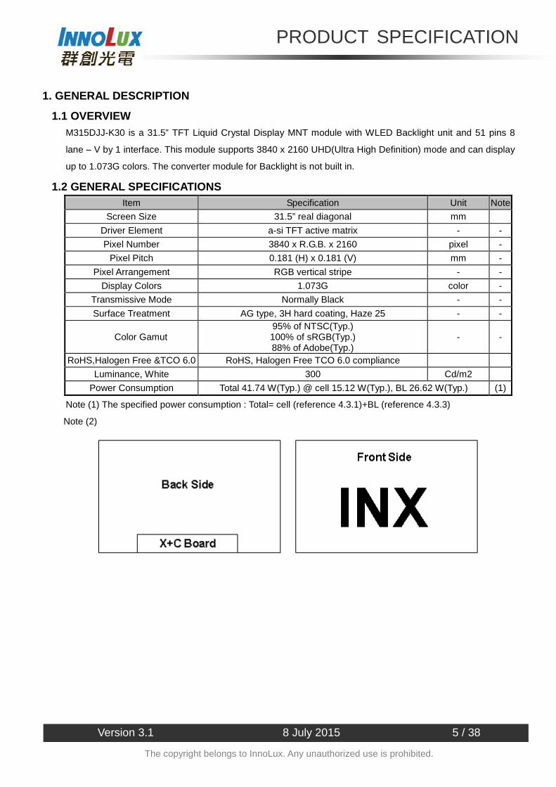
Note (2)
PRODUCT SPECIFICATION
Version 3.1 8 July 2015 6 / 38
The copyright belongs to InnoLux. Any unauthorized use is prohibited.
2. MECHANICAL SPECIFICATIONS Item Min. Typ. Max. Unit Note
Horizontal (H) 716.4 717.4 718.4 mm Vertical (V) 412.85 413.85 414.85- mm Module Size
Thickness (T) 16.9 17.9 18.9 mm (1)
Horizontal 702.4 703.4 704.4 mm Bezel Area
Vertical 396.85 397.85 398.85 mm Horizontal - 698.4 - mm
Active Area Vertical - 392.85 - mm
Weight 3287 3460 3633 g
Note (1) Please refer to the attached drawings for more information of front and back outline dimensions.
3. ABSOLUTE MAXIMUM RATINGS
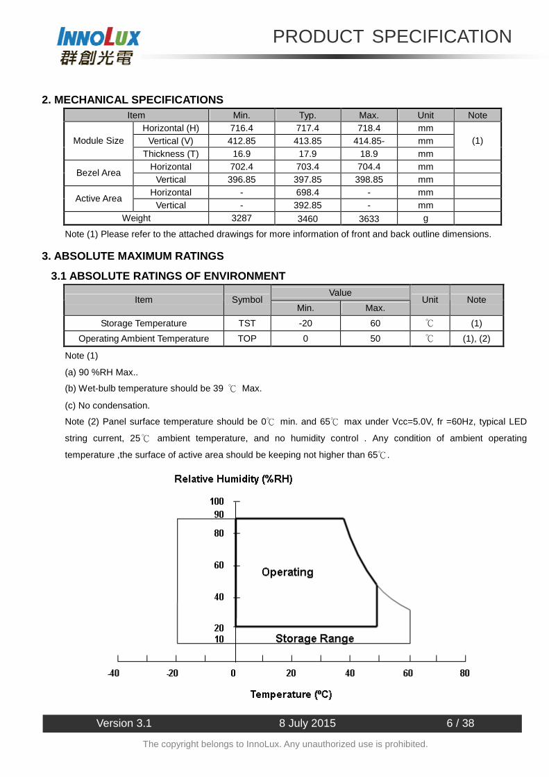
3.1 ABSOLUTE RATINGS OF ENVIRONMENT Value
Item Symbol Min. Max.
Unit Note
Storage Temperature TST -20 60 (1)
Operating Ambient Temperature TOP 0 50 (1), (2)
Note (1)
(a) 90 %RH Max..
(b) Wet-bulb temperature should be 39 Max.
(c) No condensation.
Note (2) Panel surface temperature should be 0 min. and 65 max under Vcc=5.0V, fr =60Hz, typical LED
string current, 25 ambient temperature, and no humidity control . Any condition of ambient operating
temperature ,the surface of active area should be keeping not higher than 65.

PRODUCT SPECIFICATION
Version 3.1 8 July 2015 7 / 38
The copyright belongs to InnoLux. Any unauthorized use is prohibited.
3.2 ELECTRICAL ABSOLUTE RATINGS
3.2.1 TFT LCD MODULE Value
Item Symbol Min. Max.
Unit Note
Power Supply Voltage VCCS -0.3 13.5. V
Logic Input Voltage VIN -0.3 3.6 V (1)
3.2.2 BACKLIGHT UNIT
Note (1) Permanent damage to the device may occur if maximum values are exceeded. Function operation
should be restricted to the conditions described under Normal Operating Conditions.
Note (2) Specified values are for input pin of LED light bar at Ta=25±2 (Refer to 4.3.3 and 4.3.4 for
further information).
4. ELECTRICAL SPECIFICATIONS
4.1 FUNCTION BLOCK DIAGRAM
Value Item Symbol Min. Typ Max.
Unit Note
LED Forward Current Per Input Pin
IF 103.4 110 116.6 mA (1), (2)
Duty=100%
PRODUCT SPECIFICATION
Version 3.1 8 July 2015 8 / 38
The copyright belongs to InnoLux. Any unauthorized use is prohibited.
4.2. INTERFACE CONNECTIONS PIN ASSIGNMENT
Pin Name Description Note 1 Vin Power input (+12V) 2 Vin Power input (+12V) 3 Vin Power input (+12V) 4 Vin Power input (+12V) 5 Vin Power input (+12V) 6 Vin Power input (+12V) 7 Vin Power input (+12V) 8 Vin Power input (+12V) 9 N.C. No Connection (2) 10 GND Ground 11 GND Ground 12 GND. Ground 13 GND. Ground 14 GND. Ground 15 N.C. No Connection (2) 16 N.C. No Connection (2) 17 N.C. No Connection (2) 18 N.C For internal use, no connection 19 N.C For internal use, no connection 20 N.C. No Connection (2) 21 N.C. No Connection (2) 22 N.C. No Connection (2) 23 N.C. No Connection (2) 24 N.C. No Connection (2) 25 HTPDN Hot plug detect output, Open drain. 26 LOCKN Lock detect output, Open drain. 27 GND Ground 28 RX0N 1st Pixel Negative VbyOne differential data input in area A. Lan 0 29 RX0P 1st Pixel Positive VbyOne differential data input in area A. Lan 0
(1)
30 GND Ground 31 RX1N 2nd Pixel Negative VbyOne differential data input in area A. Lan 1 32 RX1P 2nd Pixel Positive VbyOne differential data input in area A. Lan 1
(1)
33 GND Ground 34 RX2N 3rd Pixel Negative VbyOne differential data input in area A. Lan 2 35 RX2P 3rd Pixel Positive VbyOne differential data input in area A. Lan 2
(1)
36 GND Ground 37 RX3N 4th Pixel Negative VbyOne differential data input in area A. Lan 3 38 RX3P 4th Pixel Positive VbyOne differential data input in area A. Lan 3
(1)
39 GND Ground 40 RX4N 5th Pixel Negative VbyOne differential data input in area A. Lan 4 41 RX4P 5th Pixel Positive VbyOne differential data input in area A. Lan 4
(1)
42 GND Ground 43 RX5N 6th Pixel Negative VbyOne differential data input in area A. Lan 5 44 RX5P 6th Pixel Positive VbyOne differential data input in area A. Lan 5
(1)
45 GND Ground 46 RX6N 7th Pixel Negative VbyOne differential data input in area A. Lan 6 47 RX6P 7th Pixel Positive VbyOne differential data input in area A. Lan 6
(1)
48 GND Ground

PRODUCT SPECIFICATION
Version 3.1 8 July 2015 9 / 38
The copyright belongs to InnoLux. Any unauthorized use is prohibited.
Pin Name Description Note 49 RX7N 8th Pixel Negative VbyOne differential data input in area A. Lan 7 50 RX7P 8th Pixel Positive VbyOne differential data input in area A. Lan 7
(1)
51 GND Ground
Connector Information
Item Description Manufacturer FCN/ P-TWO Type part number FCN: WF23-402-5133
P-TWO: 187059-51221 User’s Mating housing part number JAE: FI-RE51HL
*Notice: There would be compatible issues if not using the indicated connectors in the matching list.
Note (1) V-by-OneR HS Data Mapping
Lan Data Stream Lan 0 1, 9, 17, ..........., 3825, 3833 Lan 1 2, 10, 18, ........., 3826, 3834 Lan 2 3, 11, 19, ........., 3827, 3835 Lan 3 4, 12, 20, ........., 3828, 3836 Lan 4 5, 13, 21, ..........., 3829, 3837 Lan 5 6, 14, 22, ........., 3830, 3838 Lan 6 7, 15, 23, ........., 3831, 3839 Lan 7 8, 16, 24, ........., 3832, 3840
Note (2) Reserved for internal use. Please leave it open.
Note (3) VbyOne HS connector pin order defined as following:
Note (4) V-by-One connector mating dimension range request is 0.93mm~1.0mm as below:
Note (5) The first pixel is odd.

PRODUCT SPECIFICATION
Version 3.1 8 July 2015 10 / 38
The copyright belongs to InnoLux. Any unauthorized use is prohibited.
Note (6) Input signal of even and odd clock should be the same timing
1,1 (odd) 1,2
(even) 1,3 (odd) 1,4
(even) 2,1 2,2
3,1
Ymax,1 Ymax, Xmax
1,Xmax
Pitch
Pitch
4.3 ELECTRICAL CHARACTERISTICS
4.3.1 LCD ELETRONICS SPECIFICATION (Ta = 25 ± 2 ºC)
Value Parameter Symbol
Min. Typ. Max. Unit Note
Power Supply Voltage VCC 10.8 12 13.2 V (1) Rush Current IRUSH - - 2.6 A (2)
White Pattern PT - 8.78 9.52 W
Black Pattern PT - 8.18 8.86 W Power Consumption
Horizontal Stripe PT - 15.12 16.38 W
(3)
White Pattern - - 0.73 0.88 A
Black Pattern - - 0.68 0.82 A Power Supply
Current Horizontal Stripe - - 1.26 1.53 A
(3)
Differential Input High Threshold Voltage VLVTH - - +50 mV
Differential Input Low Threshold Voltage VLVTL -50 - - mV VbyOne HS
Differential Input Resistor
RRIN 80 100 120 ohm
Input High Threshold Voltage
VIH 2.7 - 3.3 V CMOS
interface Input Low Threshold Voltage
VIL 0 - 0.7 V

PRODUCT SPECIFICATION
Version 3.1 8 July 2015 11 / 38
The copyright belongs to InnoLux. Any unauthorized use is prohibited.
Note (1) The module should be always operated within the above ranges. The ripple voltage should be
controlled under 10 % of Vcc (Typ.)
Note (2) Measurement Conditions
Note (3) The specified power supply current is under the conditions at Vcc = 12 V, Ta = 25 ± 2 ºC, Fr = 60Hz,
whereas a power dissipation check pattern below is displayed.
PRODUCT SPECIFICATION
Version 3.1 8 July 2015 12 / 38
The copyright belongs to InnoLux. Any unauthorized use is prohibited.
4.3.2.BACKLIGHT UNIT Value Parameter Symbol
Min. Typ. Max. Unit Note
LED Light Bar Input Voltage Per Input Pin
VPIN - 60.5 65.0 V (1),
Duty=100%, IPIN=110mA
LED Light Bar Current Per Input Pin
IPIN 103.4 110 116.6 mA (1), (2)
Duty=100% LED Life Time LLED 30000 Hrs (3)
Power Consumption PBL - 26.62 28.6 W (1)
Duty=100%, IPIN=110mA
Note (1) LED light bar input voltage and current are measured by utilizing a true RMS multimeter as shown
below:
Note (2) PBL = IPIN × VPIN × ( 4 ) input pins.
Note (3) The lifetime of LED is defined as the time when LED packages continue to operate under the
conditions at Ta = 25 ±2 and I= (150)mA (per chip) until the brightness becomes ≦ 50% of its
original value.
Note (4) The module must be operated with constant driving current.
Note (5) If converter has PWM function, the PWM Frequency setting must be over 480Hz.
4.3.3 LIGHTBAR CONNECTOR PIN ASSIGNMENT: (1) Connector Information:
Item Description Manufacturer FCN Type part number WM13-406-083N(FCN) Mating housing part number WF1300108-B (FCN)
*Notice: There would be compatible issues if not using the indicated connectors in the matching list.

PRODUCT SPECIFICATION
Version 3.1 8 July 2015 13 / 38
The copyright belongs to InnoLux. Any unauthorized use is prohibited.
(2) LB Connector drawing:
Pin number Description 1 Cathode of LED string1 2 Cathode of LED string2 3 NC 4 VLED 5 VLED 6 NC 7 Cathode of LED string3 8 Cathode of LED string4

PRODUCT SPECIFICATION
Version 3.1 8 July 2015 14 / 38
The copyright belongs to InnoLux. Any unauthorized use is prohibited.
4.4 V BY ONE INPUT SIGNAL SPECIFICATIONS
4.4.1 V BY ONE DATA MAPPING TABLE Lan Data Stream
Lan 0 1, 9, 17, ..........., 3825, 3833
Lan 1 2, 10, 18, ........., 3826, 3834
Lan 2 3, 11, 19, ........., 3827, 3835
Lan 3 4, 12, 20, ........., 3828, 3836
Lan 4 5, 13, 21, ..........., 3829, 3837
Lan 5 6, 14, 22, ........., 3830, 3838
Lan 6 7, 15, 23, ........., 3831, 3839
Lan 7 8, 16, 24, ........., 3832, 3840
PRODUCT SPECIFICATION
Version 3.1 8 July 2015 15 / 38
The copyright belongs to InnoLux. Any unauthorized use is prohibited.
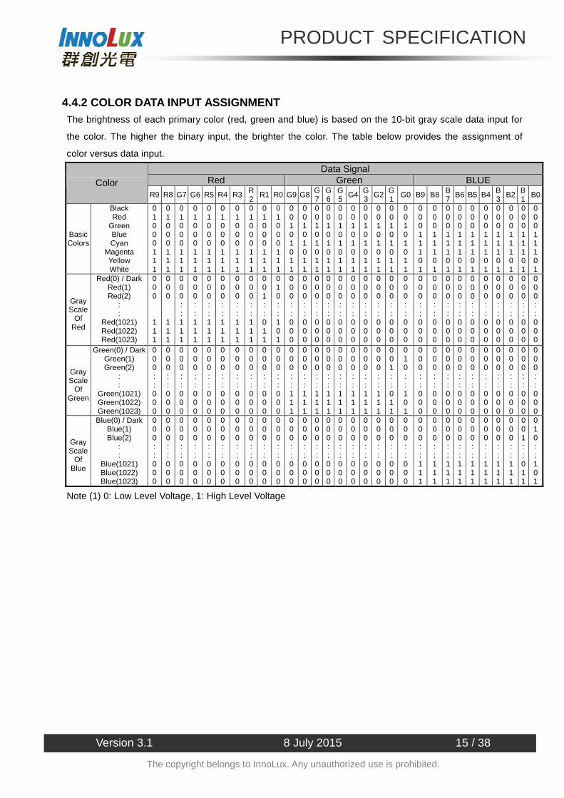
4.4.2 COLOR DATA INPUT ASSIGNMENT The brightness of each primary color (red, green and blue) is based on the 10-bit gray scale data input for
the color. The higher the binary input, the brighter the color. The table below provides the assignment of
color versus data input.
Data Signal Red Green BLUE Color
R9 R8 G7 G6 R5 R4 R3 R2
R1 R0 G9 G8 G7
G6
G5
G4 G3
G2 G1
G0 B9 B8 B7
B6 B5 B4 B3
B2 B1
B0
Basic Colors
Black Red
Green Blue Cyan
Magenta Yellow White
0 1 0 0 0 1 1 1
0 1 0 0 0 1 1 1
0 1 0 0 0 1 1 1
0 1 0 0 0 1 1 1
0 1 0 0 0 1 1 1
0 1 0 0 0 1 1 1
0 1 0 0 0 1 1 1
0 1 0 0 0 1 1 1
0 1 0 0 0 1 1 1
0 1 0 0 0 1 1 1
0 0 1 0 1 0 1 1
0 0 1 0 1 0 1 1
0 0 1 0 1 0 1 1
0 0 1 0 1 0 1 1
0 0 1 0 1 0 1 1
0 0 1 0 1 0 1 1
0 0 1 0 1 0 1 1
0 0 1 0 1 0 1 1
0 0 1 0 1 0 1 1
0 0 1 0 1 0 1 1
0 0 0 1 1 1 0 1
0 0 0 1 1 1 0 1
0 0 0 1 1 1 0 1
0 0 0 1 1 1 0 1
0 0 0 1 1 1 0 1
0 0 0 1 1 1 0 1
0 0 0 1 1 1 0 1
0 0 0 1 1 1 0 1
0 0 0 1 1 1 0 1
0 0 0 1 1 1 0 1
Gray Scale
Of Red
Red(0) / Dark Red(1) Red(2)
: :
Red(1021) Red(1022) Red(1023)
0 0 0 1 1 1
0 0 0 1 1 1
0 0 0 : : 1 1 1
0 0 0 : : 1 1 1
0 0 0 : : 1 1 1
0 0 0 : : 1 1 1
0 0 0 : : 1 1 1
0 0 0 : : 1 1 1
0 0 1 : : 0 1 1
0 1 0 : : 1 0 1
0 0 0 : : 0 0 0
0 0 0 : : 0 0 0
0 0 0 : : 0 0 0
0 0 0 : : 0 0 0
0 0 0 : : 0 0 0
0 0 0 : : 0 0 0
0 0 0 : : 0 0 0
0 0 0 : : 0 0 0
0 0 0 : : 0 0 0
0 0 0 : : 0 0 0
0 0 0 : ; 0 0 0
0 0 0 : : 0 0 0
0 0 0 : : 0 0 0
0 0 0 : : 0 0 0
0 0 0 : : 0 0 0
0 0 0 : : 0 0 0
0 0 0 : : 0 0 0
0 0 0 : : 0 0 0
0 0 0 : : 0 0 0
0 0 0 : : 0 0 0
Gray Scale
Of Green
Green(0) / Dark Green(1) Green(2)
: :
Green(1021) Green(1022) Green(1023)
0 0 0 : : 0 0 0
0 0 0 : : 0 0 0
0 0 0 : : 0 0 0
0 0 0 : : 0 0 0
0 0 0 : : 0 0 0
0 0 0 : : 0 0 0
0 0 0 : : 0 0 0
0 0 0 : : 0 0 0
0 0 0 : : 0 0 0
0 0 0 : : 0 0 0
0 0 0 : : 1 1 1
0 0 0 : : 1 1 1
0 0 0 : : 1 1 1
0 0 0 : : 1 1 1
0 0 0 : : 1 1 1
0 0 0 : : 1 1 1
0 0 0 : : 1 1 1
0 0 0 : : 1 1 1
0 0 1 : : 0 1 1
0 1 0 : : 1 0 1
0 0 0 : : 0 0 0
0 0 0 : : 0 0 0
0 0 0 : : 0 0 0
0 0 0 : : 0 0 0
0 0 0 : : 0 0 0
0 0 0 : : 0 0 0
0 0 0 : : 0 0 0
0 0 0 : : 0 0 0
0 0 0 : : 0 0 0
0 0 0 : : 0 0 0
Gray Scale
Of Blue
Blue(0) / Dark Blue(1) Blue(2)
: :
Blue(1021) Blue(1022) Blue(1023)
0 0 0 : : 0 0 0
0 0 0 : : 0 0 0
0 0 0 : : 0 0 0
0 0 0 : : 0 0 0
0 0 0 : : 0 0 0
0 0 0 : : 0 0 0
0 0 0 : : 0 0 0
0 0 0 : : 0 0 0
0 0 0 : : 0 0 0
0 0 0 : : 0 0 0
0 0 0 : : 0 0 0
0 0 0 : : 0 0 0
0 0 0 : : 0 0 0
0 0 0 : : 0 0 0
0 0 0 : : 0 0 0
0 0 0 : : 0 0 0
0 0 0 : : 0 0 0
0 0 0 : : 0 0 0
0 0 0 : : 0 0 0
0 0 0 : : 0 0 0
0 0 0 : : 1 1 1
0 0 0 : : 1 1 1
0 0 0 : : 1 1 1
0 0 0 : : 1 1 1
0 0 0 : : 1 1 1
0 0 0 : : 1 1 1
0 0 0 : : 1 1 1
0 0 0 : : 1 1 1
0 0 1 : : 0 1 1
0 1 0 : : 1 0 1
Note (1) 0: Low Level Voltage, 1: High Level Voltage
PRODUCT SPECIFICATION
Version 3.1 8 July 2015 16 / 38
The copyright belongs to InnoLux. Any unauthorized use is prohibited.
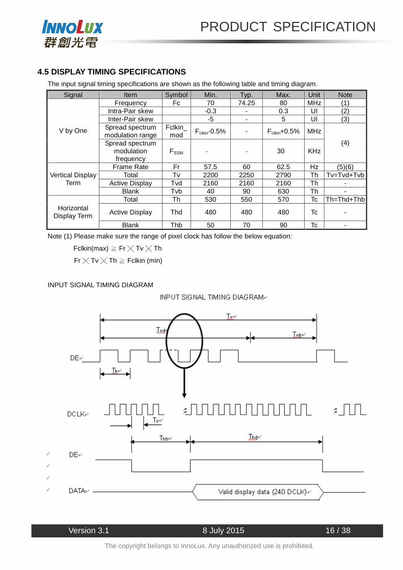
4.5 DISPLAY TIMING SPECIFICATIONS The input signal timing specifications are shown as the following table and timing diagram.
Signal Item Symbol Min. Typ. Max. Unit Note Frequency Fc 70 74.25 80 MHz (1)
Intra-Pair skew -0.3 - 0.3 UI (2) Inter-Pair skew -5 - 5 UI (3)
Spread spectrum modulation range
Fclkin_mod
Fclkin-0.5% - Fclkin+0.5% MHz V by One
Spread spectrum modulation frequency
FSSM - - 30 KHz (4)
Frame Rate Fr 57.5 60 62.5 Hz (5)(6) Total Tv 2200 2250 2790 Th Tv=Tvd+Tvb
Active Display Tvd 2160 2160 2160 Th - Vertical Display
Term Blank Tvb 40 90 630 Th - Total Th 530 550 570 Tc Th=Thd+Thb
Active Display Thd 480 480 480 Tc - Horizontal
Display Term Blank Thb 50 70 90 Tc -
Note (1) Please make sure the range of pixel clock has follow the below equation:
Fclkin(max) ≧ Fr Tv Th
Fr Tv Th ≧ Fclkin (min)
INPUT SIGNAL TIMING DIAGRAM

PRODUCT SPECIFICATION
Version 3.1 8 July 2015 17 / 38
The copyright belongs to InnoLux. Any unauthorized use is prohibited.
Note (2) V-by-One HS Intra-pair skew
Note (3) V-by-One HS Inter-pair skew
Note (4) The SSCG (Spread spectrum clock generator) is defined as below figures.
Note (5) The frame-to-frame jitter of the input frame rate is defined as the above figures. FRn = FRn-1 ±
0.5%.
Note (6) The setup of the frame rate jitter > 0.5% may result in the cosmetic LED backlight symptom and the
electric function is affected.
PRODUCT SPECIFICATION
Version 3.1 8 July 2015 18 / 38
The copyright belongs to InnoLux. Any unauthorized use is prohibited.
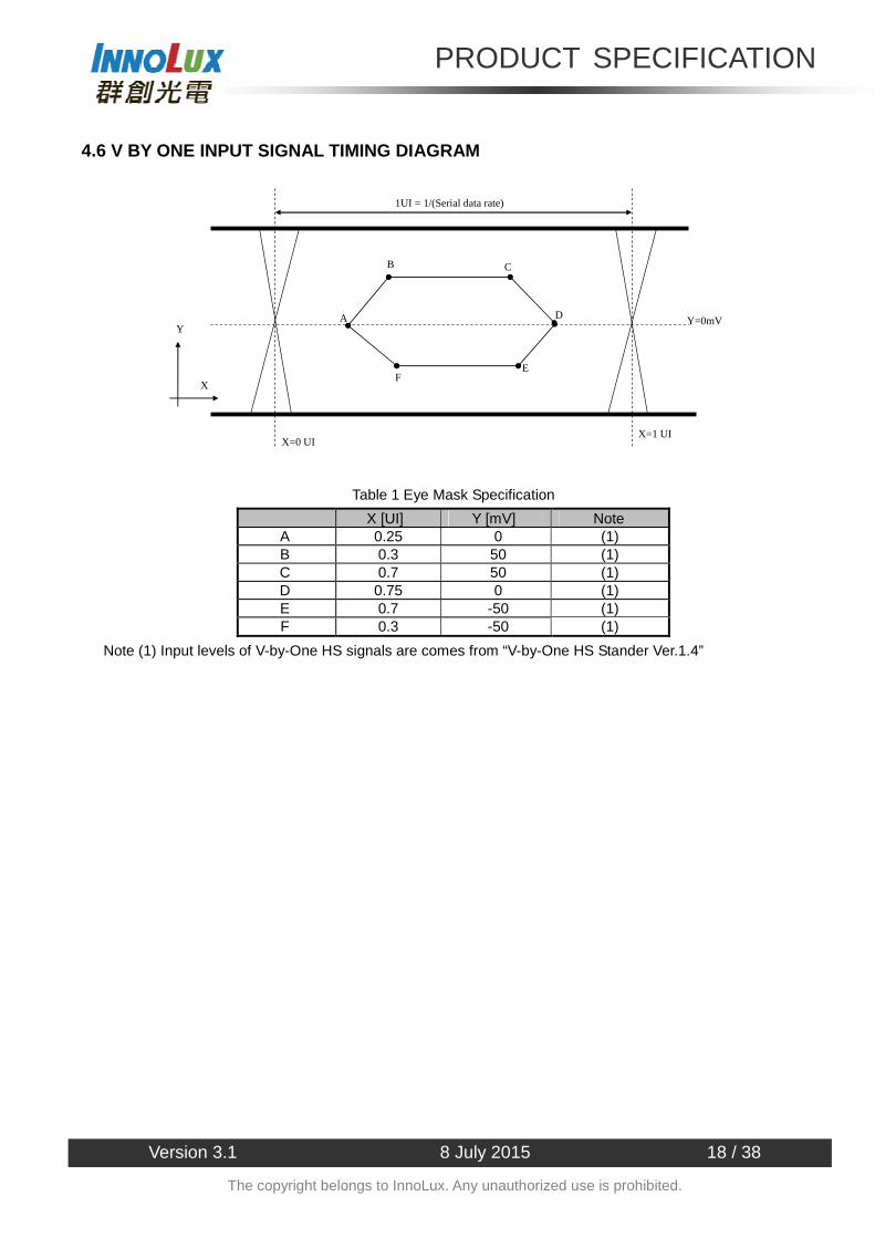
4.6 V BY ONE INPUT SIGNAL TIMING DIAGRAM
Y
X
X=0 UI X=1 UI
1UI = 1/(Serial data rate)
A
B C
D
E F
Y=0mV
Table 1 Eye Mask Specification
X [UI] Y [mV] Note A 0.25 0 (1) B 0.3 50 (1) C 0.7 50 (1) D 0.75 0 (1) E 0.7 -50 (1) F 0.3 -50 (1)
Note (1) Input levels of V-by-One HS signals are comes from “V-by-One HS Stander Ver.1.4”
PRODUCT SPECIFICATION
Version 3.1 8 July 2015 19 / 38
The copyright belongs to InnoLux. Any unauthorized use is prohibited.
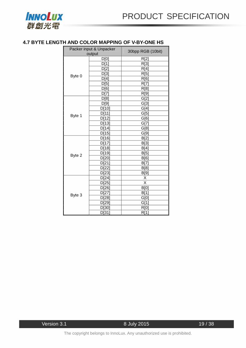
4.7 BYTE LENGTH AND COLOR MAPPING OF V-BY-ONE HS Packer input & Unpacker
output 30bpp RGB (10bit)
D[0] R[2] D[1] R[3] D[2] R[4] D[3] R[5] D[4] R[6] D[5] R[7] D[6] R[8]
Byte 0
D[7] R[9] D[8] G[2] D[9] G[3] D[10] G[4] D[11] G[5] D[12] G[6] D[13] G[7] D[14] G[8]
Byte 1
D[15] G[9] D[16] B[2] D[17] B[3] D[18] B[4] D[19] B[5] D[20] B[6] D[21] B[7] D[22] B[8]
Byte 2
D[23] B[9] D[24] X D[25] X D[26] B[0] D[27] B[1] D[28] G[0] D[29] G[1] D[30] R[0]
Byte 3
D[31] R[1]

PRODUCT SPECIFICATION
Version 3.1 8 July 2015 20 / 38
The copyright belongs to InnoLux. Any unauthorized use is prohibited.
4.8 POWER ON/OFF SEQUENCE (Ta = 25 ± 2 ºC)
To prevent a latch-up or DC operation of LCD module, the power on/off sequence should be as the diagram
below.

PRODUCT SPECIFICATION
Version 3.1 8 July 2015 21 / 38
The copyright belongs to InnoLux. Any unauthorized use is prohibited.
Note (1) The supply voltage of the external system for the module input should follow the definition of Vcc.
Note (2) Apply the LED voltage within the LCD operation range. When the backlight turns on before the LCD
operation or the LCD turns off before the backlight turns off, the display may momentarily become
abnormal screen..
Note (3) In case of Vcc is in off level, please keep the level of input signals on the low or high impedance. If
T2<0,that maybe cause electrical overstress failure.
Note (4) T4 should be measured after the module has been fully discharged between power off and on
period..
Note (5) Interface signal shall not be kept at high impedance when the power is on
Note (6) Vcc must decay smoothly when power-off
PRODUCT SPECIFICATION
Version 3.1 8 July 2015 22 / 38
The copyright belongs to InnoLux. Any unauthorized use is prohibited.
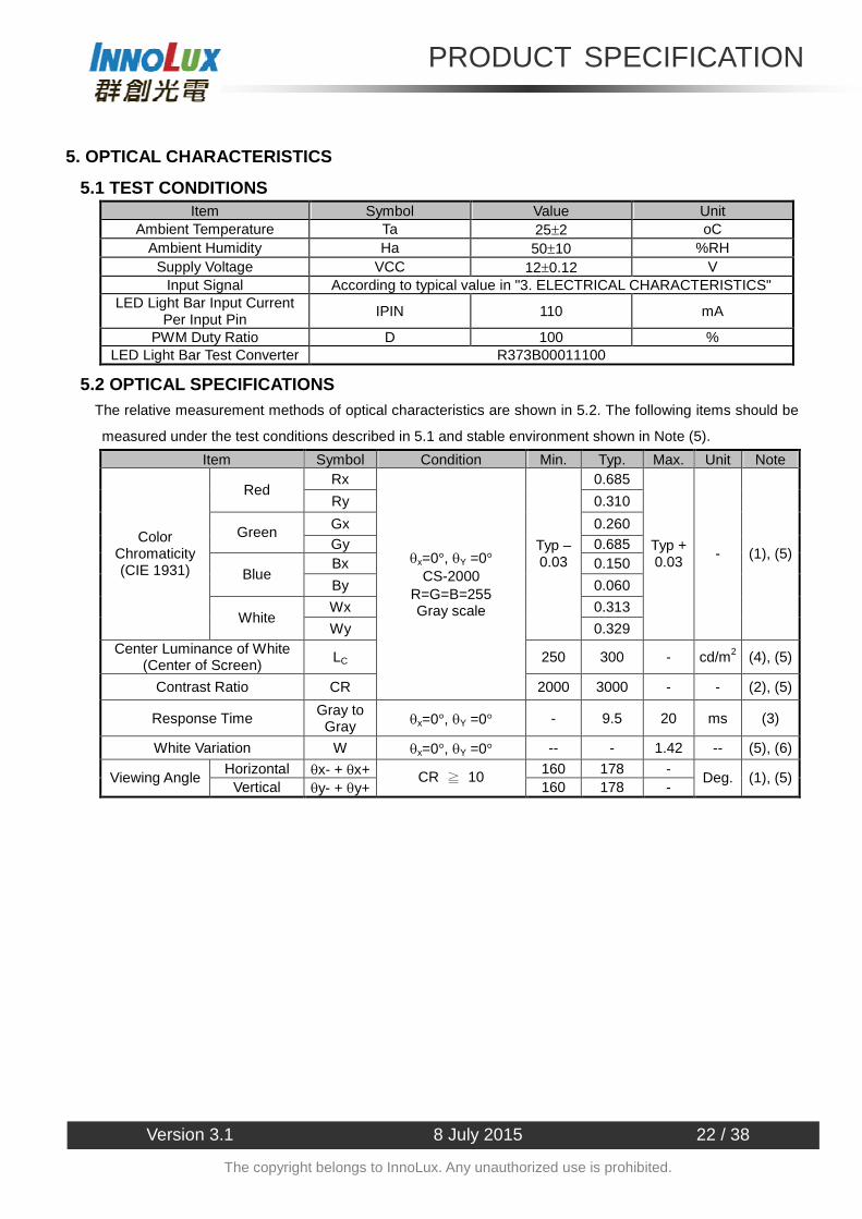
5. OPTICAL CHARACTERISTICS
5.1 TEST CONDITIONS Item Symbol Value Unit
Ambient Temperature Ta 25±2 oC Ambient Humidity Ha 50±10 %RH
Supply Voltage VCC 12±0.12 V Input Signal According to typical value in "3. ELECTRICAL CHARACTERISTICS"
LED Light Bar Input Current Per Input Pin
IPIN 110 mA
PWM Duty Ratio D 100 % LED Light Bar Test Converter R373B00011100
5.2 OPTICAL SPECIFICATIONS The relative measurement methods of optical characteristics are shown in 5.2. The following items should be
measured under the test conditions described in 5.1 and stable environment shown in Note (5).
Item Symbol Condition Min. Typ. Max. Unit Note Rx 0.685
Red Ry 0.310
Gx 0.260 Green
Gy 0.685 Bx 0.150
Blue By 0.060
Wx 0.313
Color Chromaticity (CIE 1931)
White Wy
Typ – 0.03
0.329
Typ + 0.03
- (1), (5)
Center Luminance of White (Center of Screen) LC 250 300 - cd/m2 (4), (5)
Contrast Ratio CR
θx=0°, θY =0° CS-2000
R=G=B=255 Gray scale
2000 3000 - - (2), (5)
Response Time Gray to Gray θx=0°, θY =0° - 9.5 20 ms (3)
White Variation W θx=0°, θY =0° -- - 1.42 -- (5), (6)
Horizontal θx- + θx+ 160 178 - Viewing Angle
Vertical θy- + θy+ CR ≧ 10
160 178 - Deg. (1), (5)

PRODUCT SPECIFICATION
Version 3.1 8 July 2015 23 / 38
The copyright belongs to InnoLux. Any unauthorized use is prohibited.
Note (1) Definition of Viewing Angle (θx, θy):
Note (2) Definition of Contrast Ratio (CR):
The contrast ratio can be calculated by the following expression.
Contrast Ratio (CR) = L255 / L0
L255: Luminance of gray level 255
L 0: Luminance of gray level 0
CR = CR (5)
CR (X) is corresponding to the Contrast Ratio of the point X at Figure in Note (6).
Note (3) Definition of Gray-to-Gray Switching Time:
The driving signal means the signal of gray level 0, 31, 63, 95, 127, 159, 191, 223 and 255.
Gray to gray average time means the average switching time of gray level 0, 31, 63, 95, 127, 159, 191,
223 and 255 to each other
PRODUCT SPECIFICATION
Version 3.1 8 July 2015 24 / 38
The copyright belongs to InnoLux. Any unauthorized use is prohibited.
Note (4) Definition of Luminance of White (LC):
Measure the luminance of gray level 255 at center point
LC = L (5)
L (x) is corresponding to the luminance of the point X at Figure in Note (6).
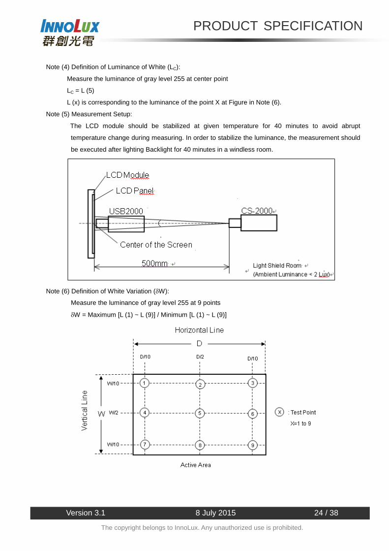
Note (5) Measurement Setup:
The LCD module should be stabilized at given temperature for 40 minutes to avoid abrupt
temperature change during measuring. In order to stabilize the luminance, the measurement should
be executed after lighting Backlight for 40 minutes in a windless room.
Note (6) Definition of White Variation (δW):
Measure the luminance of gray level 255 at 9 points
δW = Maximum [L (1) ~ L (9)] / Minimum [L (1) ~ L (9)]
PRODUCT SPECIFICATION
Version 3.1 8 July 2015 25 / 38
The copyright belongs to InnoLux. Any unauthorized use is prohibited.
6. RELIABILITY TEST ITEM Items Required Condition Note
Temperature Humidity Bias (THB) Ta= 50 , 80%RH, 240hours High Temperature Operation
(HTO) Ta= 50 , 240hours
Low Temperature Operation (LTO) Ta= 0 , 240hours
High Temperature Storage (HTS) Ta= 60 , 240hours
Low Temperature Storage (LTS) Ta= -20 , 240hours
Vibration Test (Non-operation)
Acceleration: 1.5 G Wave: sine
Frequency: 10 - 300 Hz Sweep: 30 Minutes each Axis (X, Y, Z)
Shock Test (Non-operation)
Acceleration: 50 G Wave: Half-sine
Active Time: 11 ms Direction : ± X, ± Y, ± Z.(one time for
each Axis)
Thermal Shock Test (TST) -20/30min , 60 / 30min , 100 cycles
On/Off Test 25 ,On/10sec , Off /10sec , 30,000
cycles
ESD (Electro Static Discharge) Contact Discharge: ± 8KV,
150pF(330Ω)
Air Discharge: ± 15KV, 150pF(330Ω)
Altitude Test Operation:10,000 ft / 24hours
Non-Operation:30,000 ft / 24hours
Note (1) criteria : Normal display image with no obvious non-uniformity and no line defect.
Note (2) Evaluation should be tested after storage at room temperature for more than two hour
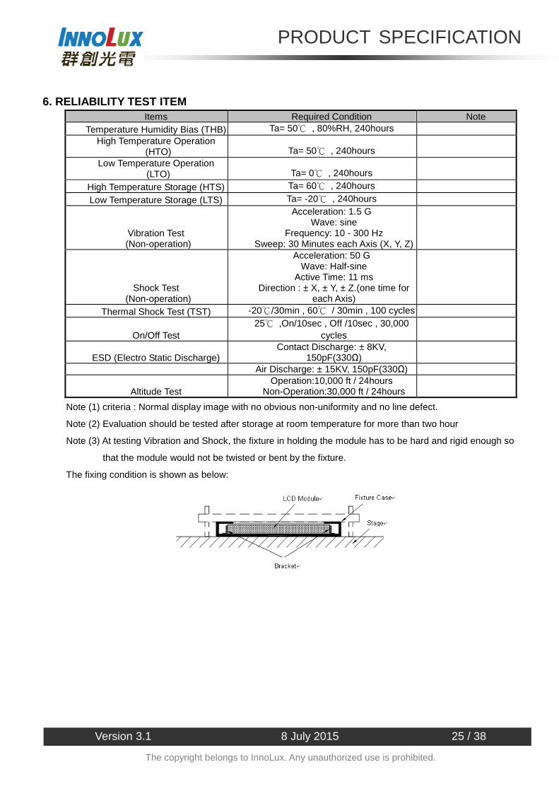
Note (3) At testing Vibration and Shock, the fixture in holding the module has to be hard and rigid enough so
that the module would not be twisted or bent by the fixture.
The fixing condition is shown as below:

PRODUCT SPECIFICATION
Version 3.1 8 July 2015 26 / 38
The copyright belongs to InnoLux. Any unauthorized use is prohibited.
7. MECHANICAL STRENGTH CHARACTERISTICS
7.1 MECHANICAL STRENGTH SPECIFICATIONS Item Condition Min Unit Note
Mechanical Strength 128th Gray Pattern 0.6 Kgf
7.2 TEST CONDITIONS Items Description
Test Condition
1. Ambient Illumination : 10~15 lux 2. Test Pattern : 128 Gray 3. Distance of the judgment : 30cm from the surface of module 4. Viewing angle of the judgment : Front
Gage Information
1. Push pull guage a. Model name : HF-50, maker : ALGOL b. Shape of gage tip - Diameter : 2mm - Thickness : 2mm
Definition of Minimum force
To measure minimum force when operator detects any white spot and light leakage that have occurred while operator presses on back side of module with push pull gage.
7.3 DEFINITION OF TEST POINTS Measure the minimum force of test points at 128th Gray pattern. The test points at back side of module area
is showing as below (If the test points on the PCBA, these points are not included)..
PRODUCT SPECIFICATION
Version 3.1 8 July 2015 27 / 38
The copyright belongs to InnoLux. Any unauthorized use is prohibited.
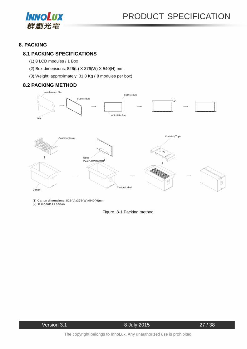
8. PACKING
8.1 PACKING SPECIFICATIONS (1) 8 LCD modules / 1 Box
(2) Box dimensions: 826(L) X 376(W) X 540(H) mm
(3) Weight: approximately: 31.8 Kg ( 8 modules per box)
8.2 PACKING METHOD
(1) Carton dimensions: 826(L)x376(W)x540(H)mm(2) 8 modules / carton
LCD Module
Anti-static Bag
CartonCarton Label
Cushion(down)
LCD Module
panel protect film
tape
Figure. 8-1 Packing method

PRODUCT SPECIFICATION
Version 3.1 8 July 2015 28 / 38
The copyright belongs to InnoLux. Any unauthorized use is prohibited.
8.3 PALLET For ocean shipping
Air Transportation
2 Layer
Corner Protector
PP Belt
(L1080*50*50mm ,t=7mm)
(L1150*W850*140mm,田田田)
(L1000*50*50mm ,t=7mm)
Sea / Land Transportation (40ft HQ Container) Sea / Land Transportation (40ft Container)
3+2 Layer 3 Layer
Corner Protector
(L1350*50*50mm ,t=3mm)
PP Belt
(L1150*W850*140mm,田田田)
Corner Protector
PP Belt
(L1080*50*50mm ,t=7mm)
(L1150*W850*140mm,田田田)
(L1000*50*50mm ,t=7mm)
Figure. 8-2 Packing method

PRODUCT SPECIFICATION
Version 3.1 8 July 2015 29 / 38
The copyright belongs to InnoLux. Any unauthorized use is prohibited.
8.4 UN-PACKING METHOD
Figure. 8-3 UN-Packing method

PRODUCT SPECIFICATION
Version 3.1 8 July 2015 30 / 38
The copyright belongs to InnoLux. Any unauthorized use is prohibited.
9. INX MODULE LABEL The barcode nameplate is pasted on each module as illustration, and its definitions are as following
explanation.
(a) Model Name: M315DJJ-K30
(b) Revision: Rev. XX, for example: A0, A1… B1, B2… or C1, C2…etc.
(c) InnoLux barcode definition:
Serial ID: XX-XX-X-XX-YMD-L-NNNN
Code Meaning Description
XX InnoLux internal use -
XX Revision Cover all the change
X InnoLux internal use -
XX InnoLux internal use -
YMD Year, month, day Year: 0~9, 2001=1, 2002=2, 2003=3…2010=0, 2011=1, 2012=2…
Month: 1~12=1, 2, 3, ~, 9, A, B, C Day: 1~31=1, 2, 3, ~, 9, A, B, C, ~, W, X, Y, exclude I, O, and U.
L Product line # Line 1=1, Line 2=2, Line 3=3, …
NNNN Serial number Manufacturing sequence of product
(d) Customer’s barcode definition:
Serial ID: CM-V5J30-X-X-X-XX-L-XX-L-YMD-NNNN
Code Meaning Description
CM Supplier code INX=CM
V5J30 Model number M315DJJ-K30= V5J30
X Revision code Non ZBD: 1,2,~,8,9 / ZBD: A~Z
X Source driver IC code
X Gate driver IC code
Century=1, CLL=2, Demos=3, Epson=4, Fujitsu=5, Himax=6, Hitachi=7, Hynix=8, LDI=9, Matsushita=A, NEC=B, Novatec=C,
OKI=D, Philips=E, Renasas=F, Samsung=G, Sanyo=H, Sharp=I, TI=J, Topro=K, Toshiba=L, Windbond=M, ILITEK=Q, Fiti=Y, None IC =Z
XX Cell location Tainan Taiwan=TN, Ningbo China=CN, Hsinchu Taiwan=SC
L Cell line # 1,2,~,9,A,B,~,Y,Z
XX Module location Tainan, Taiwan=TN , Ningbo China=NP, Shenzhen China=SH,
Nanhai China=NH
L Module line # 1,2,~,9,A,B,~,Y,Z
YMD Year, month, day Year: 0~9, 2001=1, 2002=2, 2003=3…2010=0, 2011=1, 2012=2…
Month: 1~12=1, 2, 3, ~, 9, A, B, C Day: 1~31=1, 2, 3, ~, 9, A, B, C, ~, T, U, V
NNNN Serial number By LCD supplier

PRODUCT SPECIFICATION
Version 3.1 8 July 2015 31 / 38
The copyright belongs to InnoLux. Any unauthorized use is prohibited.
(e) FAB ID(UL Factory ID):
Region Factory ID
TWINX GEMN
NBCMI LEOO
NBCMI VIRO
NBCME CANO
NHCMI CAPG
10. PRECAUTIONS
10.1 ASSEMBLY AND HANDLING PRECAUTIONS (1) Do not apply rough force such as bending or twisting to the module during assembly.
(2) To assemble or install module into user’s system can be only in clean working areas. The dust and oil
may cause electrical short or worsen the polarizer.
(3) It’s not permitted to have pressure or impulse on the module because the LCD panel and Backlight will
be damaged.
(4) Always follow the correct power sequence when LCD module is connecting and operating. This can
prevent damage to the CMOS LSI chips during latch-up.
(5) Do not pull the I/F connector in or out while the module is operating.
(6) Do not disassemble the module.
(7) Use a soft dry cloth without chemicals for cleaning, because the surface of polarizer is very soft and
easily scratched.
(8) It is dangerous that moisture come into or contacted the LCD module, because moisture may damage
LCD module when it is operating.
(9) High temperature or humidity may reduce the performance of module. Please store LCD module within
the specified storage conditions.
(10)When ambient temperature is lower than 10ºC may reduce the display quality. For example, the
response time will become slowly.
(11) While touching the panel surface under the patterns with higher grey levels, a shadow or mura
phenomenon would be seen.This phenomenon is totally recoverable by switching the patterns to lower
grey levels. It is a product feature
10.2 STORAGE PRECAUTIONS (1) Do not leave the module in high temperature, and high humidity for a long time. It is highly recommended
to store the module with temperature from 0 to 35 and relative humidity of less than 70%
(2) Do not store the TFT – LCD module in direct sunlight
(3) The module should be stored in dark place. It is prohibited to apply sunlight or fluorescent light in storing

PRODUCT SPECIFICATION
Version 3.1 8 July 2015 32 / 38
The copyright belongs to InnoLux. Any unauthorized use is prohibited.
10.3 OPERATION PRECAUTIONS (1) The LCD product should be operated under normal condition.
Normal condition is defined as below :
Temperature : 20±15
Humidity: 65±20%
Display pattern : continually changing pattern(Not stationary)
(2) If the product will be used in extreme conditions such as high temperature,high humidity,high
altitude ,display pattern or operation time etc…It is strongly recommended to contact INX for application
engineering advice . Otherwise , Its reliability and function may not be guaranteed.
10.4 SAFETY PRECAUTIONS (1) If the liquid crystal material leaks from the panel, it should be kept away from the eyes or mouth. In case
of contact with hands, skin or clothes, it has to be washed away thoroughly with soap.
(2) After the module’s end of life, it is not harmful in case of normal operation and storage.
10.5 SAFETY STANDARDS The LCD module should be certified with safety regulations as follows:
Requirement Standard remark UL UL60950-1:2006 or Ed.2:2007
cUL/CSA CAN/CSA C22.2 No.60950-1-03 or 60950-1-07 CB IEC60950-1:2005 / EN60950-1:2006+ A11:2009
10.6 OTHER When fixed patterns are displayed for a long time, remnant image is likely to occur.

PRODUCT SPECIFICATION
Version 3.1 8 July 2015 33 / 38
The copyright belongs to InnoLux. Any unauthorized use is prohibited.
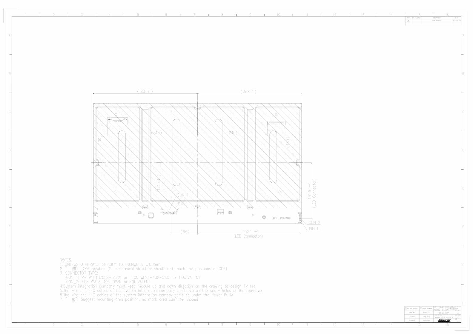
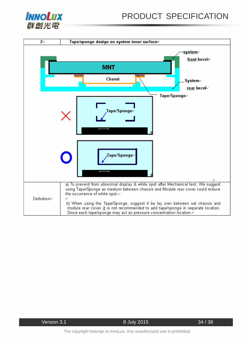
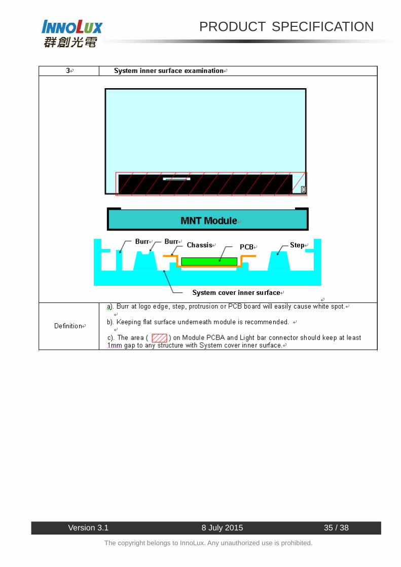
Appendix 1. SYSTEM COVER DESIGN NOTICE
PRODUCT SPECIFICATION
Version 3.1 8 July 2015 34 / 38
The copyright belongs to InnoLux. Any unauthorized use is prohibited.
PRODUCT SPECIFICATION
Version 3.1 8 July 2015 35 / 38
The copyright belongs to InnoLux. Any unauthorized use is prohibited.

PRODUCT SPECIFICATION
Version 3.1 8 July 2015 36 / 38
The copyright belongs to InnoLux. Any unauthorized use is prohibited.
Appendix 2. OUTLINE DRAWING