modeling and control method for high-power electromagnetic
TRANSCRIPT

Journal of Power Electronics, Vol. 13, No. 4, July 2013 679
http://dx.doi.org/10.6113/JPE.2013.13.4.679
JPE 13-4-19
Modeling and Control Method for High-power Electromagnetic Transmitter Power Supplies
Fei Yu† and Yi-ming Zhang*
†*College of Electronic Information and Control Engineering, Beijing University of Technology, Beijing, China
Abstract
High-power electromagnetic transmitter power supplies are an important part of deep geophysical exploration equipment. This is
especially true in complex environments, where the ability to produce a highly accurate and stable output and safety through redundancy have become the key issues in the design of high-power electromagnetic transmitter power supplies. To solve these issues, a high-frequency switching power cascade based emission power supply is designed. By combining the circuit averaged model and the equivalent controlled source method, a modular mathematical model is established with the on-state loss and transformer induction loss being taken into account. A triple-loop control including an inner current loop, an outer voltage loop and a load current forward feedback, and a digitalized voltage/current sharing control method are proposed for the realization of the rapid, stable and highly accurate output of the system. By using a new algorithm referred to as GAPSO, which integrates a genetic algorithm and a particle swarm algorithm, the parameters of the controller are tuned. A multi-module cascade helps to achieve system redundancy. A simulation analysis of the open-loop system proves the accuracy of the established system and provides a better reflection of the characteristics of the power supply. A parameter tuning simulation proves the effectiveness of the GAPSO algorithm. A closed-loop simulation of the system and field geological exploration experiments demonstrate the effectiveness of the control method. This ensures both the system’s excellent stability and the output’s accuracy. It also ensures the accuracy of the established mathematical model as well as its ability to meet the requirements of practical field deep exploration. Key words: Cascade, Current sharing, Modeling, Triple-loop control, Voltage sharing
I. INTRODUCTION Electromagnetic exploration is the most effective
geophysical exploration technique used in the search for metal mineral resources, underground freshwater resources, geothermal fields, as well as the detection of geological disasters. In equipment for electromagnetic exploration, electromagnetic transmitters reverse a steady power supply with a desired frequency and emit the energy through grounding electrodes, in order to obtain an effective electromagnetic field for deep geophysical exploration [1]-[3]. To obtain effective geophysical data from deep exploration, the transmitter needs to be high-voltage and high-current, with a highly accuracy output. These requirements bring technical difficulties to the development of power supplies. Conventionally, non-controlled rectification and excitation
adjustment are applied in the design of a high-power transmitter power supply. However, this approach complicates the manufacturing and control of the power generator, reduces the controllability of the output voltage and the reliability of the system, and causes inconvenience in the transportation of equipment during filed geological exploration.
With the development of high-frequency switching power supplies, their merits of energy efficient, small size, excellent dynamic performance, strong adaptability, etc. have made them popularly in inverter welding machines, high-frequency heating power, electrically operated power supplies and other electronic application fields [4]-[8]. For the development of switching power supplies, digitalizing and modularizing are the current guidelines, especially the series-parallel of multiple power supply modules, which has become a hot topic in the studies of power supplies. Studies have shown that using high-frequency power supply technology and modular design have become the trend in designing transmitter power supplies [8]-[10]. However, such designs usually employ analog devices to control the voltage/current sharing, which adds complexity to the circuit. This also introduces potential problems to the
Manuscript received Jan.21, 2013; revised May 8, 2013 Recommended for publication by Associate Editor Se-Kyo Chung. †Corresponding Author: [email protected] Tel: +86-180-1015-8718, Beijing University of Technology *College of Electronic Information and Control Engineering, Beijing University of Technology, China

680 Journal of Power Electronics, Vol. 13, No. 4, July 2013 stability and safety of a system when it operates in the field for a long period of time. Meanwhile, the earth load exhibits different impedances at different frequencies. Thus ensuring high-accuracy and a stable output from a transmitter power supply in harsh environments has become a key topic in the design of geophysical exploration instruments.
Based on the high-frequency, modularizing, and digitalizing trends of switching power supplies, an electromagnetic transmitter power supply has been designed and its control in complex environments has been studied. First, the topology of the electromagnetic transmitter is introduced, and the mathematic model of a single module of the power supply is established. Then, using triple-loop control including an inner current loop, an outer voltage loop and load current forward feedback, and based on the requirements of series-parallel and voltage/current sharing, a digital voltage/current sharing method is employed to realize the control of the output balance. Finally, simulation and experimental results validate both the correctness of the established model and the effectiveness of the control method. They also demonstrated that the electromagnetic transmitter power supply designed in this study can meet the practical needs of field geological exploration.
II. TOPOLOGY OF THE TRANSMITTER
Considering the practical needs of field deep exploration projects, the transmitter designed in this study has performance indicators of 20KW, 0-1000V wide range stable output. For a high-frequency switching power supply with a high-voltage high-power output, the isolated step-up full-bridge converter topology shown in Fig. 1 is adopted. This kind of topology has a larger step-up ratio and a wider voltage adjustment range. It is highly reliable and widely employed on occasions where a high-voltage high-power output is needed such as in electroplating electrolysis, electrically operating and power testing [4]-[7]. However, as a current-mode topology, it has many shortcomings: (1) It has a startup control problem. The output capacitor voltage is zero when the circuit is started. The boost inductor’s energy cannot be transferred to the load, resulting in a boost inductor current that cannot be controlled. This causes the inductor to be easily saturated or even damaged. As a result, the system needs additional starting circuit, thereby increasing the complexity of the circuit. (2) It has an inductor magnetic reset problem. The converter normally stops working or its failure results in a sudden power switch shutdown. The inductor needs to use the magnetic reset circuit to release the stored energy or the inductor produces high voltage stress that damages the components. Then the inductor needs an additional magnetic reset circuit, thereby increasing the complexity of the circuit. (3) It has a large step-up ratio problem. A large step-up ratio results in a low duty ratio when the system is running with a low voltage output. The low duty
ratio and high-power output situation significantly reduces the efficiency of the power supply and affects the reliability and stability of the system. (4) It also has a component selection problem. The maximum output voltage of the system is up to 1000V, making the selection of the secondary rectifier bridge devices of the transformer extremely difficult.
In view of the above shortcomings of the isolated step-up full-bridge converter topology, a switching frequency of 20KHZ and a full-bridge DC-DC converter are chosen for the transmitter. The system employs a two-way full-bridge converter cascade. The two-way converters are completely symmetrical with consistent parameters. The input is parallel, and the series or parallel output is controlled by a relay. The last stage of the inverters emits energy into the earth at a certain frequency in order to obtain the data needed for geological exploration. The topology of the transmitter is as shown in Fig. 2.
The DC voltage obtained by passing a three-phase AC through an uncontrolled rectifier can be treated as equivalent to a constant voltage source. Thus the system’s modular structure is equivalent to a full-bridge converter, as shown in Fig. 3. The modularized design can help to simplify the structure, reduce costs, and achieve system redundancy. When a transmitter emits in the high voltage range (500-1000V), the parallel input and series output structure is employed. The output current of a single module is equal to the output current of a series-connected transmitter, and the output voltage is the sum of all modules’ output voltage. When the transmitter emits in the range of low voltage (0-500V), the parallel input and parallel output structure is employed. the output voltage of a single module is equal to the output voltage of a parallel-connected transmitter, and the output current is the sum of all the modules’ output current.
III. SYSTEM MODELING The modeling analysis of a switching converter is the
foundation of switching power supply studies because of its great significance in the analysis and design of switching power supplies. Early DC-DC switching converter modeling methods are mainly circuit the averaged modeling, state space method, PWM switching averaged modeling, etc. With the development of switching converter technology, an equivalent controlled source method has emerged recently, and it has been widely applied [11]-[13]. In this study, the circuit averaged
· ·
Fig. 1. Topology of isolated step-up full-bridge converter.

Journal of Power Electronics, Vol. 13, No. 4, July 2013 681
modeling and equivalent controlled source methods are combined for the modeling analysis of a system. This takes into account the on-state loss of the full-bridge converter and the inductance loss of the transformer. The modeling process is elaborated below: (1) Convert the non-ideal devices into an equivalent series of ideal devices and their parasitic parameters. Non-ideal power switches should be converted into a series of ideal switches and the on-state resistance. Non-ideal diodes should be converted to a series of ideal switches, the forward voltage drop, and the forward resistance. The conduction loss and primary windings of the transformer should be series-connected at the primary side of the ideal transformer, and the secondary windings should be series-connected at the secondary side of the ideal transformer.
(2) Based on the principle of conservation of energy, derive the on-state resistance of the switch transistors, the forward voltage drop of the diodes, the forward resistance, and the equivalent average value of the primary and secondary windings of the transformer in the large signal averaged model. Then, convert the values into the inductance branch in order to simplify the model.
(3) Using the circuit substitution theorem, perform alternative replacement of the ideal switches with the controlled voltage source and controlled current source. The controlled current source and voltage source are the average time of the entire cycle.
(4) To make the model concise and practical, replace the
controlled voltage source and current source with an ideal transformer.
A. Large Signal Model Assume a full-bridge converter switch transistor
( ) ( )1 4 2 3, , ,S S S S , with a switching cycle of T, a switching
frequency of 1sf T= , an on-state time of ont , a turn-off time
of offt , where on offT t t= + , and a duty ratio of ontTD = . The
IGBT and the output capacity of the diodes are neglected, the on-state resistance onR is linear, and the turn-off resistance is infinite. The on-state status of the IGBT diodes and rectifier diodes are simulated by the linear forward resistance FR and
the forward voltage FV , when the turn-off resistance is infinite. The distributed capacity and core loss of the transformer are neglected. In the entire switching process, the inductance current is constant.
Then, the equivalent circuit of the full-bridge converter is as shown in Fig. 4, where 1 2,T TR R are the resistances of the
primary and secondary windings of the converter, LR is the
equivalent series resistance of inductor L, CR is the equivalent
series resistance of the filter capacitor, kL is the primary
conduction loss of the transformer, and FV is the forward on-state voltage drop of the diodes.
g g
gg
g
gg
gg
1: n
gg
g
g
g
g
g
gg
gg
g
gg
ggg g
Fig. 2. Topology of the Transmitter.
1S
2S
3S
4S
1: n
L
C R oViV · ·+
-
1zD 2zD
3zD 4zD4D
3D1D
2D
AB
Si
Fig. 3. Structure of full-bridge converter
·
·
·
iV
onR
2 FV
2 FV 2TR
2TR
2 FR
2 FR LR L
CRR
C
·
·
onR
onRonRFRFR
FR FR
FV
FVFV
FV
kL1TR
Fig. 4. Equivalent circuit of full-bridge converter.

682 Journal of Power Electronics, Vol. 13, No. 4, July 2013
In a single switching cycle, the inductance loss can cause both duty ratio loss and a period of reverse voltage of the primary voltage of the transformer when the IGBT is in the turn-off status. Derived from Figure 5, the duty ratio loss of the voltage of the secondary windings of the transformer is:
1 2 k L sl
i
t nL I fDT V
= = (1)
The effective duty ratio loss of the voltage of the secondary windings of the transformer is:
2 k L se l
i
nL I fD D D DV
= - = - (2)
The effective current passed through one group of IGBT is:
( )2
21,4 0
13
l
l
D T DTi lS rms L L eD T
k
V DI t dt ni dt nI DT L
é ùæ öê ú= + = +ò òç ÷ê úè øë û
(3)
The effective current of the first-stage DC bus is: 2=3Srms L e lI nI D D+ (4)
The effective current of the high-frequency rectifier bridge diodes is:
2,3 2,3
20
1 42 12 3Z rms Z
T LD D e l
II i dt D DT
= = + +ò (5)
The effective current of the IGBT diodes is:
( )5
1,4 4
2
41
3rms
t i lD L Lt
k
V DI ni t t dt nIT L
é ù= + - =ò ê ú
ë û (6)
The effective primary current of the transformer is: 4 23rms L l eI nI D D= + (7)
The on-state loss of the IGBT diodes is:
t
t
1, 4S 2,3S
iV
iVABV
t
1,4Si
LnI
t
1,4Di LnI
1t ont 2t2T
3t 4t 5t T0 t
LnI
Si
1,4ZDi
LI
2LI
Fig. 5. Waveform of the switching status of the full-bridge converter.

Journal of Power Electronics, Vol. 13, No. 4, July 2013 683
1
22 2
3rms
lD D F F L
n DP I R R I×= = × (8)
The on-state loss of the secondary windings and the rectifier diodes is:
( )2
22
42 1 23
4T
e l F T
D L
D D R RP I
æ ö+ + +ç ÷è ø= (9)
The on-state loss of the IGBT is:
2 21
13S e l on LP n D D R Iæ ö= +ç ÷
è ø (10)
The on-state loss of the primary windings is:
2 2 21 1 1
423T T Srms e l T LP R I n D D R Iæ ö= = +ç ÷
è ø (11)
According to the principle of the conservation of energy and the principle of the averaging equivalence circuit, the total equivalent resistance ER and the total voltage FEV , which are series-connected with inductors in the averaged model, can be obtained from Equations (8)-(11).
( )
2 21
22
1 44 23 3
4 1 2 2 +3 2 3
E e l on e l T
l F e l F T L
R D D R n n D D R
D n R D D R R R
æ ö æ ö= + × + +ç ÷ ç ÷è ø è ø
æ ö+ × × + + + × +ç ÷è ø
(12)
( )2 1FE l FV nD V= + (13)
1l
dTD i e id T
v nV dt nd VT
= =ò (14)
11,4 10
1 12
ont tiS L l e Lt
k
Vi tdt ni dt D D niT Lé ù æ ö= + = + ×ò òê ú ç ÷
è øë û (15)
2 4
2 5
2
2
1 2 2 2Tt t T
S Ti i i i idT t tv V dt V dt V dt V dt V
Tæ ö
= + + + =ç ÷è øò ò ò ò (16)
In this set of equations, Sv is the average equivalent voltage drop of a group of IGBTs which on-state and turn-off at the same time, 1,4Si is the average equivalent current that
passes through a group of IGBTs, and Dv is the average equivalent voltage drop at the ends of a group of rectifier diodes. The equivalent simplified circuit of the system is presented in Fig. 6.
Convert the controlled source with the equivalent ideal transformer. The full-bridge large signal averaged model which includes the on-state loss and the induction loss of the transformer is as presented in Fig. 7.
B. Small Signal Model
Apply the components ^
iv and ^
ov to the input voltage iV
and output voltage oV of the large signal averaged model and the following equations are obtained:
^ ^ ^ ^ ^ ^ ^l L
S e L L L iL e L e li
nD Ii nI d nD i nI d nD i nD i vV
= + = + - + (17)
iV
FEVER L
CRR
CoV
+
-
DvSv
DvLi
Si
+
+
-
-
Sv
iV
Fig. 6. Equivalent simplified circuit of the system.
L
+
-2 iV
FEV
CR
R
ER
CoV· ·
Si
1: end
^
Li
Fig. 7 Large signal averaged model.
^ ^ ^ ^ ^ ^22 2 2 2 2l ie i L i ii e i l e
L
nDVnV d nD v nV d i nD v nD vI
+ = - + + (18)
From Equation (17), (18) and Fig. 7, the small signal circuit model of the system under the continuous conduction mode is derived and presented in Fig. 8.
The transfer function of ( )^d s and the output voltage
( )^
ov s is:
( ) ( )( ) ( )
( )
( ) ( )
^
^
^
0
2
2 1
2 2
i
ovd
v s
in C
l i l iC C E C E
L L
v sG s
d snV R sCR
nDV nDVs R R LC s L RR C R R R C R RI I
=
= =
× × +é ùæ ö
+ + + + + + + + +ê úç ÷è øë û
(19)
Let ( ) ( )^ ^
0, 0iv s d s= = , the output impedance is:
( )( )
( ) ( )2
21
2 2
o
l iC E
L
l i l iC C E C E
L L
Z snDVR sR C R sLI
nDV nDVs R R LC s L RR C R R R C R RI I
=æ ö
+ + +ç ÷è ø
é ùæ ö+ + + + + + + + +ê úç ÷
è øë û(20)
The transfer function of ( )^d s and the output current ( )
^
Li s is:
( ) ( )( ) ( )
( )
( ) ( )
^
^
^
0
2
2 (1 )
2 2
i
Lid
v s
in C
l i l iC C E C E
L L
i sG s
d snV s R R C
nDV nDVs R R LC s L RR C R R R C R RI I
=
= =
× + +é ùæ ö
+ + + + + + + + +ê úç ÷è øë û
(21)

684 Journal of Power Electronics, Vol. 13, No. 4, July 2013
2nPWMiV
2
14 k sn L f
1sL
-
ER
1R
1CR
sC+
-oV
· ·
- -
Fig. 9. Open-loop diagram of the system.
Where, the break frequency of the system is:
( )
2 l iE
Lo
C
nDV R RIR R LC
w+ +
=+
,
the damping ratio ( )
( )
2
22
l iC E C
L
l iE C
L
nDVL RR C R R R CI
nDV R R R R CI
x
æ ö+ + + +ç ÷
è ø=æ ö
+ + +ç ÷è ø
,
and the quality factor
( )
( )
2
2
l iE C
L
l iC E C
L
nDV R R R R CI
QnDVL RR C R R R CI
æ ö+ + +ç ÷
è ø=æ ö
+ + + +ç ÷è ø
.
IV. CONTROL METHOD OF THE SYSTEM The open-loop diagram of the system, as presented in Fig. 9,
can be derived from Fig. 7. Since the equivalent resistance ER is fairly small, the system can be treated as equivalent to an undamped second-order oscillation loop. At this time, the disturbance-suppression ability of the system is quite weak. Thus effective control must be applied in order to enlarge the damping ratio of the system, so that it can fulfill the speed and stability requirements.
A. Control Method The dual-loop control mode including an outer voltage loop
and an inner current loop controls the system by the sampling filter inductor/capacitor current and the filter capacitor voltage. This is done by using the control signal of the outer voltage loop error to control the current, and forcing the output voltage to follow the reference voltage by adjusting the current. The
inner current loop can enlarge the bandwidth of the control system and improve the dynamic response performance of the system [14]-[17]. This method has been widely employed for high-performance switching power supplies.
Choosing the capacitor current as the inner-loop feedback variable can make the current be tracked quickly. As a result, the output voltage is corrected in advance and benefits from the rapid response of the current. However, this grants the system a strong load capacity, and it cannot provide over-current protection to the output current [17]. Transmitter power supplies need to operate in the field for long time. As a result, over-current protection must be in place so that the safety of the equipment can be ensured. However, the over-current protection for the system output limits the output filter inductor current. Based on these considerations, the inductor current is chosen as the inter-loop feedback in this study. However, since the inductor current is the sum of the capacitor current and the load current, abrupt changes in the load current can also be suppressed while the capacitor current change is suppressed. This results in softer external characteristics of the system. To improve the load disturbance tolerance of the system, a triple-loop control approach, which includes an inner current loop, an outer voltage loop, and a load current forward feedback loop, is employed.
The closed-loop control diagram of the system is as presented in Figure 10. The outer voltage loop adjusts the instantaneous output voltage to keep track with a given reference value; the inner current loop increases the system’s damping coefficient and improve the system’s stability; the load current forward feedback loop rapidly tracks the given reference value of the inner current loop, and by combining the inductor current feedback, it tracks the given values of the capacitor current. Meanwhile the amplitude limit part actually limits the inductor current. The module output has the toughest external characteristics, and the output voltage is independent of the load.
When all of the modules use the same topology and components, their efficiency are basically the same. However, at the start-up of the system or at the earth load changing moments, the imbalance of the output may very likely cause damage to the transmitter power supply, and endanger the safety of the equipment. Therefore, voltage/current sharing
· ·
1: enD^
LnI d
- +
: ^
LlnD i
^2 i
e
Vd
D -
^2 iv
-
^2 ilnD v
^2 l iL
L
nDVi
I^
Si
^l L
i
i
nD Iv
V
L
+
-
CR
R
ER
CoV
^
Li
Fig. 8. Small signal circuit model.

Journal of Power Electronics, Vol. 13, No. 4, July 2013 685
control must be applied to the system’s cascade. For output-parallel systems, the main current sharing
methods are the droop method, the average current method, and the master-slave set method [18]-[21]. The droop method adjusts the external characteristics of each module’s output and it has poor load regulation to the combination system. The master-slave set method has weak fault-tolerant performance. The average current method has softer external characteristics of the output and the system wiring is complex. As for output- series systems, the main voltage sharing methods are the shared duty ratio method, the master-slave set method, and the average voltage method [22]-[24]. However, methods using hardware control usually complicate the system structure, and are not easily implemented.
By combining the idea of digitalized control, the average current method is revised on the basis of the triple-loop control method, making it adaptable for both voltage sharing and
current sharing. For output-parallel systems, the given signals for each module’s inductor current are averaged and then used as a benchmark current shared by all of the modules. As a result, the inductor currents of the modules track the same benchmark and reach consensus. When the output filter capacitors of the modules are equivalent, the output currents are also the same and current-sharing is achieved. For output-series systems, the feedback of each module’s output voltage is the 1/N times the system output. By excluding the process of averaging the inter-loop inductor currents, the synchronization of the control signals can be ensured because of the digitalized control. Therefore the voltage sharing can be controlled easily, and the approach is easy to implement. The general control diagram is as shown in Fig. 11.
B. Parameter Tuning The parameter selection for the controller directly influences
PI PWMK LI
2
14 k sn L f
1sL-
ER
1
oZ
1CR
sC+
-oV
· ·+
-
refVPI
+ + + +
oI
-·
·
·
-
Fig. 10. Closed-loop control diagram of the system.
PI PWMK LI
2
14 k sn L f
1sL-
ER
1
oZ
1CR
sC+
-oV
· ·+
-
refVPI
+ + + +
oI
-·
·
·
12
rI-+
refVPI
+ + +PI PWMK LI
2
14 k sn L f
1sL-
ER
1
oZ
1CR
sC+
-
oV· ·
+
-
+
oI
-·
·
·
-
-
·
+
+
+
·
Fig. 11. General control diagram of the system.

686 Journal of Power Electronics, Vol. 13, No. 4, July 2013 the control ability of the system. Currently the parameter tuning for a PID controller has been combined with natural computation methods such as neural networks, genetic algorithms, immune algorithms, particle swarm optimization, ant colony algorithms, quantum computing and so on. These are very promising research areas in the development of intelligent PID control [25]-[27].
A Genetic Algorithm (GA) is an artificial intelligence technology solving problems by simulating the biological evolution process and mechanisms based on the natural selection and natural genetic theories in biology. Due to its simple ideology and easy implementation, it has been widely used in optimization, machine learning, adaptive control and other engineering practices [25]. A Particle Swarm Optimization (PSO) algorithm finds the optimal solution through collaboration and information sharing between individuals. It is an evolutionary computation technique and because of its easy implementation and small amount of parameter adjustments, it is widely employed in function optimization, neural network training, fuzzy system control and other applications [26], [27]. However, genetic algorithms usually have poor efficiency in the late searching period and immature convergence. In addition, PSO algorithms usually have the shortcomings of premature convergence and poor convergence performance.
In this study, a PSO algorithm and a genetic algorithm are combined to form the proposed Genetic Particle Swarm Optimization (GAPSO) algorithm to optimize the parameters of the dual-loop controller. First, a PSO algorithm is used to update the outstanding individuals in the group and to assign them to the next generation, while other individuals are eliminated. Then the updated individuals receive conducted crossover and mutation through a genetic algorithm, and the same number of offspring are assigned to the next generation. This new algorithm protects the excellent individuals in the group and ensures diversity of the group. Thus it can prevent premature convergence of the algorithm, and avoid the danger of becoming a local optimization. The elaborated procedure of the algorithm is as presented in Fig. 12.
(1) Encode the parameters of the controller. The initial group containing Ps individuals is generated.
(2) Calculate the fitness function value for each individual in the group. Retain the first Ps/2 individuals with a higher fitness and eliminate the rest of the group.
(3) Update the velocity and position of the retained individuals and assign them to the next generation.
(4) Randomly choose two individuals from the Ps/2 individuals in the next generation. Then have them undergo crossover with the probability of Pc and generate two new individuals. Repeat this until Ps/2 offspring are generated.
(5) Perform mutation on the obtained Ps/2 offspring with the probability of Pm. After the mutation, these offspring are then assigned to the next generation and become the individuals of
the next generation group. (6) If the obtained group meets the end conditions or reaches
a preset number of iterations, stop the procedure, otherwise repeat the procedure from step (2).
V. SIMULATION ANALYSIS The main parameters for the simulation are: the input
voltage Vi=310V, the output voltage of the power supply is 600V, the earth impedance is 50Ω, and the emission current is 12A. Therefore, for each single module of the system the output voltage Vo=300V, the load R=25Ω, and the output current IL=12A.
The measured values of the parameters for the full-bridge converter module are: the resistance of the primary windings of the transformer RT1=35mΩ, the resistance of the secondary windings of the transformer RT2=72mΩ, the inductance loss of the transformer L=1.3μH, the transform ratio n=2, the switching frequency fs=20KHZ, the filter inductance L=400μH, the filter capacity C=100μF, the capacitor equivalent series resistance Rc=10mΩ, the inductor inner-resistance RL=80mΩ, the IGBT on-state inner-resistance Ron=10mΩ, the high-frequency rectifier diode on-state inner-resistance Rf=6.1mΩ, and the on-state voltage drop VF=1V.
1) When the induction loss kL increases, lD and
( )oZ jw increase, ( )vdG jw decreases, the resonance peaks
of the curve in the Bode diagram of ( )vdG s and ( )oZ s decrease, and the phase angle change in the oscillation loop
2SP
2 1SP +
2 1SP +2SP
PSO
sP
sP
Crossover MutationGA
N+1 Generation
N Generation
Fig. 12. Workflow of the algorithm.
TABLE I
LOW-FREQUENCY ASYMPTOTE DATA
Lk
/uH n De Dl D
Gvd(0) /V
Zo(0) /Ω
1.3 2 0.2435 0.002 0.2455 1230 0.204 4 0.1218 0.004 0.1258 2401 0.795 6 0.0812 0.006 0.0872 3464 1.72
0 2 0.2435 0 0.2435 1240 0 8 2 0.2436 0.012 0.2560 1180 1.211
Journal of Power Electronics, Vol. 13, No. 4, July 2013 687
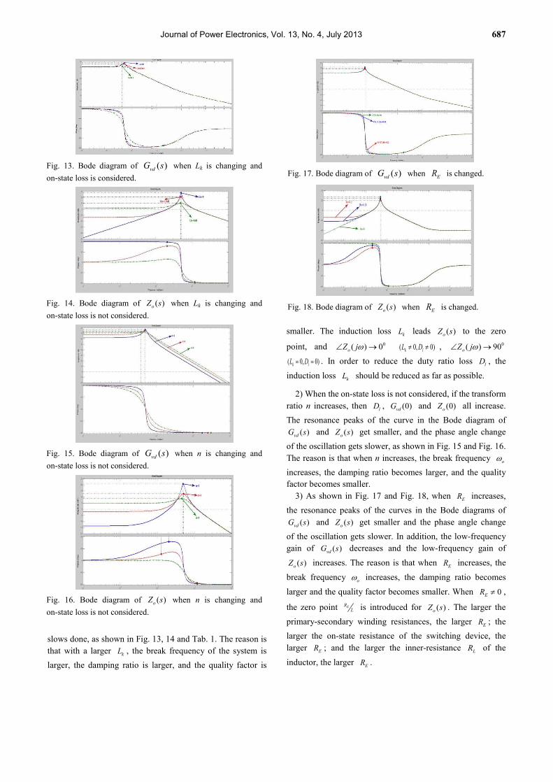
slows done, as shown in Fig. 13, 14 and Tab. 1. The reason is that with a larger kL , the break frequency of the system is larger, the damping ratio is larger, and the quality factor is
smaller. The induction loss kL leads ( )oZ s to the zero
point, and 0( ) 0oZ jwÐ ® ( 0, 0)k lL D¹ ¹ , 0( ) 90oZ jwÐ ® ( 0, 0)k lL D= = . In order to reduce the duty ratio loss lD , the
induction loss kL should be reduced as far as possible.
2) When the on-state loss is not considered, if the transform ratio n increases, then lD , (0)vdG and (0)oZ all increase. The resonance peaks of the curve in the Bode diagram of
( )vdG s and ( )oZ s get smaller, and the phase angle change of the oscillation gets slower, as shown in Fig. 15 and Fig. 16. The reason is that when n increases, the break frequency ow increases, the damping ratio becomes larger, and the quality factor becomes smaller.
3) As shown in Fig. 17 and Fig. 18, when ER increases, the resonance peaks of the curves in the Bode diagrams of
( )vdG s and ( )oZ s get smaller and the phase angle change of the oscillation gets slower. In addition, the low-frequency gain of ( )vdG s decreases and the low-frequency gain of
( )oZ s increases. The reason is that when ER increases, the
break frequency ow increases, the damping ratio becomes
larger and the quality factor becomes smaller. When 0ER ¹ ,
the zero point ERL is introduced for ( )oZ s . The larger the
primary-secondary winding resistances, the larger ER ; the larger the on-state resistance of the switching device, the larger ER ; and the larger the inner-resistance LR of the
inductor, the larger ER .
Fig. 13. Bode diagram of ( )vdG s when Lk is changing and on-state loss is considered.
Fig. 14. Bode diagram of ( )oZ s when Lk is changing and on-state loss is not considered.
Fig. 15. Bode diagram of ( )vdG s when n is changing and on-state loss is not considered.
Fig. 16. Bode diagram of ( )oZ s when n is changing and on-state loss is not considered.
Fig. 17. Bode diagram of ( )vdG s when ER is changed.
Fig. 18. Bode diagram of ( )oZ s when ER is changed.

688 Journal of Power Electronics, Vol. 13, No. 4, July 2013
TABLE II
ITERATION COMPARISON
1000 times of iteration; 60 individuals;
ITSE+IAE PSO GA GAPSO
Optimal fitness 11 5.6 1.9 Number of iteration 260 780 11
Fig. 19. Fitness comparison.
Fig. 20. Comparison of closed-loop response under variable load.
In summary, the analysis of the simulation results is in accordance with the derivation results. This would indicate that the equivalent model with the on-state loss and the transformer induction loss considered can more accurately reflect the characteristics of the full-bridge converter.
The voltage single-loop control is adopted for the full-bridge controller module to search for the optimized PI controller parameters through a comparison of the GA, the PSO algorithm, and the GAPSO algorithm, with 1000 iterations and 60 individuals. The performance indicator is the sum of the Integral Time Square Error (ITSE) and the Integral Absolute Error (IAE).
It can be seen from Fig. 19 and Tab. 2 that the GAPSO algorithm has the fastest convergence speed and the highest accuracy. In addition, when the same target error is received, the number of iterations required by the GAPSO convergence is significantly smaller.
By applying triple-loop control and the dual-loop control to the control module of the single-group full-bridge converter module, the controller parameters are tuned using the deducted mathematical model and the GAPSO algorithm.
Fig. 21 Comparison of Bode diagrams of closed-loop ( )vdG s output.
Fig. 22. Bode diagram of the output impedance of triple-closed-loop system.
It can be seen from Fig. 20 that when compared with the dual-loop control system, the triple-loop control system has a faster response speed and a smaller overshoot. Fig. 21 shows that the frequency curve of the triple-loop control system barely varies when the frequency is low, and that the curve drops rapidly after it passes the end frequency earlier than the dual-loop control system. Meanwhile, the phase frequency curve shows little phase angle change when the frequency is low. This indicates that the triple-loop control system has good stability and a strong turbulence tolerance ability. Fig. 22 shows that at the low-frequency stage, the closed-loop output impedance is small. In addition, the output voltage’s change with the load is small, the output voltage’s accuracy is good, and the ripple is small.
Alter the equivalent resistance of one group of modules when the system output is series-connected and apply the voltage-sharing control to the system. Then the simulation diagram of the system with a variable load is as shown in Fig. 23. When the system output is parallel-connected, apply the current-sharing control to the system, then the simulation diagram of the system with a variable load is as shown in Fig. 24. It can be seen that the system demonstrates an excellent voltage/current sharing effect, a fast dynamic response, and the ability to realize voltage sharing or current sharing rapidly.
VI. EXPERIMENTAL VALIDATION By using a DSP2312 to control the emission power supply,

Journal of Power Electronics, Vol. 13, No. 4, July 2013 689
with an adjustable output voltage spanning a range of 0 to 1000V, the inverse emission bridge can emit energy into the earth with different frequencies and receive GPS signals simultaneously. Simultaneous emitting and receiving experiments are performed in order to obtain the parameters for geological exploration. The physical image of the system is presented in Fig. 25. Long-term field experiments were carried out at Guan, Hebei and Xingcheng, Liaoning, China, with an average daily emitting time of 8 hours. It was observed that when the system is emitting with different frequencies, the emitting voltage can ensure the stability and accuracy of the system output when the earth impedance change is dramatic.
It can be seen from Fig. 26 and 27 that the voltage/current sharing control method of the system received excellent results in practical application. The time required for voltage/current sharing control adjustment is very short, which satisfies the requirements of practical applications perfectly. Fig. 28 shows that when the load variance is large, the DC bus has a small fluctuation, which demonstrates the high accuracy and strong load turbulence tolerance ability of the control system. As can be seen from Fig. 29, 30, and 31, during the emissions of the transmitter, the overshot of the output is small, the adjustment time is short, the accuracy is good, the fluctuations when stable are small, and the load turbulence tolerance ability is strong. Meanwhile, the stable output of the system also demonstrates the correctness of the established mathematical model.
Fig. 25. Physical image of the system.
Fig. 26. Measured waveform of current-sharing control.
Fig. 27. Measured waveform of voltage-sharing control.
Fig. 28. Bus voltages with variable load of the system.
Fig. 29. Low frequency emission waveform of the system.
Fig. 23. Diagram of voltage sharing with variable load.
Fig. 24. Diagram of current sharing with variable load.

690 Journal of Power Electronics, Vol. 13, No. 4, July 2013
Fig. 30. Medium frequency emission waveform of the system.
Fig. 31. High frequency emission waveform of the system.
VII. CONCLUSIONS With high-power high-frequency switching power supply
technology, a high-power electromagnetic transmitter power supply with a switching frequency of 20KHZ and a power of 20KW was designed based on the requirements of practical field geological exploration. A two-stage full-bridge converter module cascade was employed for the system. The continuous small signal mathematic model of the system was established by combining the circuit averaged model and the equivalent controlled source method while taking into account the on-state loss of the system and the induction loss of the transformer. The closed-loop control model of the system was established by using the triple-loop control structure including an outer voltage loop, an inner current loop and load current forward feedback. When the modules are parallel-connected, a uniform averaged reference current is adopted to achieve the uniform current sharing of the modules. When the modules are series-connected, the feedback signal of each module is 1/N times the output signal of the system. Thus the uniform voltage sharing feedback is achieved, and the response speed and accuracy of the output control are improved. Simulation analysis and field experiments proved the accuracy of the established mathematical model, the accuracy of the controller parameter tuning with the GAPSO algorithm, and the effectiveness of the control method. While ensuring a highly stable output, the accuracy of the system is also ensured. Meanwhile, it was demonstrated that the designed high-power electromagnetic transmitter power supply can meet the requirements of practical wild geological exploration perfectly.
REFERENCES [1] Z. Chen and H. Dong, “Development of novel transient
electromagnet tiansmitter,” Progress in Exploration Geophysics, Vol. 27, No. 6, pp. 444-446, Dec. 2004.
[2] G. Tan, Z. Fu, and L. Zhou, “A design of control for transient electromagnetic transmitter,” Electrical Measurement & Instrumentation, Vol. 43, No. 483, pp. 8-12, Mar. 2006.
[3] P. Lin, P. Guo, and F. Shi, “A study of the techniques for large-depth and multi-functional electromagnetic survey,” Acta Geoscientica Sinica, Vol. 4, No. 31, pp. 149-154, Apr. 2010.
[4] S. Wang, “Rectifier-preferred Power Supply for Cleaner Production in Electroplating Industry,” Electroplating & Finishing, Vol. 26, No. 7, pp. 39-41, Jul. 2007.
[5] F. Ma, A. Luo, and H. Xiao, “High-power high-efficient and simplified high-frequency switching power supply for electrolytic plating,” Proceedings of the CSEE, Vol. 32, No. 21, pp. 71-78, Jul. 2012.
[6] P. Hu, Z. Wang, and H. Chen, “Output-voltage-regulated Full-bridge DC-DC Converter,” Journal of Mechanical & Electrical Engineering, Vol. 28, No. 9, pp. 1153-1156, Jan. 2011.
[7] X. Jiang, “Research on the topology theory and control technonogy of isolated boost full bridge dc-dc converter,” PhD. Thesis, Beijing: Institute of Electrical Engineering, Chinese Academy of Sciences, 2006.
[8] C. Ouyang, “Analysis & study on modeling of DC-DC switching converter,” PhD. Thesis, NAN Jing: Nanjing University of Aeronautics & Astronautics, 2005.
[9] Z. Fu and L. Zhou, “Two novel quasi-resonant steep current impulse rectifying circuits,” Proceedings of the CSEE, Vol. 26, No. 5, pp. 70-75, Feb. 2006.
[10] D. Bai, “The effect of two types of turn-off current on TEM responses and the correction techniques,” Seismology and Geology, Vol. 23, No. 2, pp. 245-251, Jun. 2001.
[11] D. Voncina and J. Nastran, “Current source for pulse plating with high di/dt and low ripple in steady state,” Industrial Electronics, 1999, ISIE99, Proceedings of the IEEE International Symposium on Volume 2, pp. 753-756, 1999.
[12] X. Wang, Y. Zou, and J. Liu, “Modeling and control of full-bridge DC/DC switching power supply,” Power Electronics, Vol. 41, No. 7, pp. 86-88, Aug. 2007.
[13] J. Zhou and X. Zeng, “A review of the modeling and analysis of DC-DC switching power converters,” Journal of South China University of Technology (Natural Science Edition), Vol. 28, No. 8, pp. 111-116, Aug. 2000.
[14] D. P. Argo, I. Pandu, and S. Yukihiko, “A control method for single-phase PWM inverters,” Proceedings of the International Conference on Power Electronics and Drive Systems, pp. 282-285, 2001.
[15] R. Chen, W. Liang, and Z. Wei, “Study of inverter with dual-loop control,” Telecom Power Technologies, Vol. 23, No. 1, pp. 19-21, Sep. 2006.
[16] O. Kukrer and H. Komurcugil, “Control strategy for single-phase UPS inverters,” Electric Power Application, IEEE Proc. pp. 743-746, 2003.
[17] H. Yang and J. Song, “Modeling and simulation of a single-phase voltage PWM inverter based on dual-loop control,” Electric Drive Automation, Vol. 31, No. 1, pp. 15-18, Apr. 2009.
[18] J. W. Kim, H. S. Choi and B. H. Cho, “A novel droop method for converter parallel operation,” IEEE Trans. Power Electron., Vol. 17, No. 1, pp. 25-32, Nov. 2001.

Journal of Power Electronics, Vol. 13, No. 4, July 2013 691
[19] Y. Panov and M. Jovanov, “Stability and dynamic performance of current-sharing control for paralleled voltage regulator modules,” IEEE Trans. Power Electron., Vol. 17, No. 2, pp. 172-179, Mar. 2002.
[20] C. Lin and C. Chen, “Single-wire current-share paralleling of current-mode-controlled DC power supplies,” IEEE Trans. Ind. Electron., Vol. 47, No. 4, pp. 780-786, Mar. 2000.
[21] Y. Huang and C. K. Tse, “Circuit theoretic classification of parallel connected DC-DC converters,” IEEE Trans. Circuits Syst. I, Reg. Papers, Vol. 54, No. 5, pp. 1099-1108, Jul. 2007.
[22] L. Zheng, S. Zhao and J. Zhu, “Research on Input-paralleled Output-series Half-bridge Converter,” High Voltage Engineering, Vol. 34, No. 7, pp. 1483-1488, Jul. 2008.
[23] J. Kang, C. Roh and G. Moon, “Phase-shifted parallel-input/series-output dual converter for high power step-up applications,” IEEE Trans. Ind. Appl., Vol. 49, No. 3, pp. 649-652, Aug. 2002.
[24] X. Kong and A. Khambadkone, “Analysis and implementation of a high efficiency, interleaved current-fed full bridge converter for fuel cell system,” IEEE Trans. Power Electron., Vol. 22, No. 2, pp. 543-550, Mar. 2007.
[25] W. DU and Z. Han, “Float-point genetic algorithm with self-adaptive crossover operator,” Journal of System Simulation, Vol. 18, No. 6, pp. 1711-1713, Jul. 2006.
[26] Y. Cen, Y. Qin and D. Sun, “Application of PSO algorithm in wavelet neural network,” Journal of System Simulation, Vol. 16, No. 12, pp. 2783-2788, Feb. 2004.
[27] W. Xiong and B. Xu, “Study on optimization of SVR parameters selection based on PSO,” Journal of System Simulation, Vol. 18, No. 9, pp. 2442-2445, Nov. 2006.
Fei Yu was born in Hubei, China, in 1985. He received his B.E. and M.E. from the College of Electrical and Electronic Engineering, Wuhan Institute of Technology, Wuhan, China in 2006 and 2009, respectively. He is currently working towards his Ph.D. in the College of Electronic Information and Control Engineering,
Beijing University of Technology, Beijing, China. He is participating in research dealing with quality control of electrical equipment, electric tests and tests on the electromagnetic compatibility of electrical and electronic equipment. His current research interests include modeling and control of switching power supplies, system optimization concerning electromagnetic fields and high voltages.
Yi-ming Zhang was born in Hubei, China, in 1964. He received his B.E. from the School of Electronic, Information and Electrical Engineering, Shanghai Jiao Tong University, Shanghai, China, in 1988, and his M.E. from the School of Electrical Engineering and Automation, Harbin Institute of Technology, Harbin, China in 1992. From 2000 to 2007,
he was a Senior Researcher in the Institute of Electrical Engineering, Chinese Academy of Sciences, Beijing, China. Since 2008, he has been an Professor in the College of Electronic Information and Control Engineering, Beijing University of Technology, Beijing, China. His current research interests include intelligent power management, motor speed control, servo drives and motor energy conservation.