molecular sensing using monolayer floating gate, fully depleted soi mosfet acting as an exponential...
TRANSCRIPT

Molecular Sensing Using MonolayerFloating Gate, Fully Depleted SOIMOSFET Acting as an ExponentialTransducerBharath R. Takulapalli†,*
Center for Solid State Electronics Research, Science and Engineering of Materials, Arizona State University, Tempe, Arizona 85287. †Current address: Biodesign Institute,Arizona State University, Tempe, AZ 85287
Current day science and technologyhas far surpassed human sensorycapabilities of sight, sound, and
touch, while electronic technologies that
mimic sense of smell and taste have largely
remained a challenge. The urgency for ul-
trahigh sensitive sensor devices for chemi-
cal, biological, radiological, nuclear, and ex-
plosive (CBRNE) detection in homeland
security and military applications, and the
paradigm of point-of-care diagnostics in fu-
ture healthcare are two major drivers for ad-
vance research in chemical and biological
sensors. Consequently, an increased num-
ber of new material technologies that are
capable of label-free single molecule level
sensing are reported.1�3 However, none of
the technologies available today satisfies all
of the requirements for a robust sensing
platform, viz. high sensitivity, high selectiv-
ity, reusability, inexpensive manufacturing,
miniaturization, systems-on-chip integra-
tion capability, and so on. In this paper, we
present a new field-effect device concept as
a possible solution to some of these chal-
lenges in the field of chemical and biologi-
cal sensing.
Field-effect sensors work on the general
principle of detecting shifts in localized
electric potential due to chemical interac-
tions at the device surface. A chemical-
sensitive thin film deposited on the device
surface undergoes a specific chemical inter-
action with the target species, causing a
change in the charge polarization inside the
thin film and a corresponding shift in elec-
trochemical potential at the device
surface�thin film interface. The resultant
change in electric field at the device sur-
face modulates the density of charge carri-
ers in the semiconductor conduction chan-nel beneath it. In the case of chemiresistoror Schottky-type field-effect sensors,4�8 thedetection of target species is due to thefield-effect modulation of channel majoritycharge carrier density, that is, chemical bind-ing events at the device surface leading toaccumulation and depletion of majoritycharge carriers in the semiconductor con-duction channel. MOSFET-type sensors onthe other hand are operated with the semi-conductor channel biased in inversion.9�11
In this type of device, target molecule bind-ing at the chemical-sensitive device surfacemodulates the minority charge carrier den-sity in the inversion channel. In either case,this Coulombic field-effect modulation ofcharge carriers in the conduction channel,characterized by the carrier Debye length,produces a corresponding change in con-duction current measured across the
*Address correspondence [email protected].
Received for review July 31, 2009and accepted January 5, 2010.
Published online January 19, 2010.10.1021/nn900901f
© 2010 American Chemical Society
ABSTRACT Field-effect transistor-based chemical sensors fall into two broad categories based on the principle
of signal transductionOchemiresistor or Schottky-type devices and MOSFET or inversion-type devices. In this
paper, we report a new inversion-type device conceptOfully depleted exponentially coupled (FDEC) sensor, using
molecular monolayer floating gate fully depleted silicon on insulator (SOI) MOSFET. Molecular binding at the
chemical-sensitive surface lowers the threshold voltage of the device inversion channel due to a unique capacitive
charge-coupling mechanism involving interface defect states, causing an exponential increase in the inversion
channel current. This response of the device is in opposite direction when compared to typical MOSFET-type
sensors, wherein inversion current decreases in a conventional n-channel sensor device upon addition of negative
charge to the chemical-sensitive device surface. The new sensor architecture enables ultrahigh sensitivity along
with extraordinary selectivity. We propose the new sensor concept with the aid of analytical equations and present
results from our experiments in liquid phase and gas phase to demonstrate the new principle of signal
transduction. We present data from numerical simulations to further support our theory.
KEYWORDS: field effect · sensors · pH sensing · exponentialtransduction · sensitivity · selectivity · FDEC
ARTIC
LE
www.acsnano.org VOL. 4 ▪ NO. 2 ▪ 999–1011 ▪ 2010 999

channel source�drain regions, enabling the detection
of target species.
When using SOI thin film field-effect devices in sens-
ing applications, the top thin film silicon can be oper-
ated in four different regimes of interest: (1) in accumu-
lation, (2) inversion with partial depletion of Si film, (3)
inversion with full depletion of the Si film, and (4) in vol-
ume inversion mode where the whole of Si film is in-
verted. Our work discusses the device response in the
case of inversion with full depletion of the Si thin film. We
present here a new class of field-effect devices for
chemical sensing applications, termed fully depleted
exponentially coupled (FDEC) sensors using porphyrin
monolayer floating gate fully depleted SOI MOSFET. In
these novel MOSFET-based sensor devices, ligand bind-
ing at the device surface modulates the inversion
threshold voltage of the device via a second-order ca-
pacitive charge-coupling mechanism involving inter-
face defect states, resulting in an exponential increase
in the device response. This response of the device is in
opposite direction when compared to typical MOSFET-
type sensors, wherein inversion current decreases in a
conventional n-channel device upon addition of nega-
tive charge to the chemical-sensitive device surface.
A conventional thin film SOI MOSFET is a bi-gate
structure with the silicon thin film sandwiched be-
tween top gate insulator and the buried oxide
(BOX).12,13 The substrate silicon contact acts as an addi-
tional gate with buried oxide (BOX) as its gate oxide.
Unlike a regular MOS transistor, the thin film SOI transis-
tor is a two interface problem, viz. top gate
oxide�silicon channel interface and BOX�silicon thin
film interface. When the silicon thin film is fully de-
pleted, the two interfaces are strongly coupled, en-
abling control of either interface with its correspond-
ing secondary gate. In our work, the SOI thin film is
boron-doped (p-type 1015 cm�3) 100 nm in thickness,
and the top gate of the regular SOI MOSFET is replaced
with zinc(II) 5,10,15,20-tetra(3-
carboxylphenyl)porphyrin (ZnTCPP) molecular mono-
layer that now acts as a floating gate; details reported
elsewhere.14 Native oxide (NO) layer that is grown over
the active silicon surface, underneath the molecular
monolayer, acts as the corresponding monolayer gate
oxide (Figure 1a). Electron inversion channel is estab-
lished at the bottom silicon thin film�BOX interface
by applying positive bias to the substrate silicon
contact.
Analytical Model. Threshold voltage (Vt) of a conven-
tional MOS transistor varies directly with the cumula-
tive charge in the depletion region and at its bound-
aries, specifically charge at the Si channel�gate oxide
interface. Variation of threshold voltage with charging
and discharging of donor and acceptor-like interface
trap states located at the gate oxide�silicon interface
is well understood.15 In our case of substrate-gate-
biased fully depleted SOI FET, even charge at the na-
tive oxide (NO)�silicon interface, particularly due to in-
terface states, needs to be considered in evaluating
the threshold voltage of inversion channel formed at
the bottom Si�BOX interface. When a net amount of
charge is added to the molecular monolayer or to the
surface of the native oxide, it causes charging and dis-
charging of interface states at the NO�silicon film inter-
face due to the high capacitance of the very thin na-
tive oxide layer,15,16 ca. 2 nm. Addition of negative
charge to the molecular monolayer causes charging of
donor-like interface trap states (neutral when filled, be-
low EF) and discharging of acceptor-like interface
charge states (neutral when empty, above EF) in
p-silicon, that is, a net increase of positive charge at
the NO�Si interface. This in turn causes a decrease in
threshold voltage of inversion channel formed at the
Si�BOX interface according to �Vt � ��Q/Ceff, where
�Q is the net charge added at the NO�Si interface and
Ceff is the effective capacitance.
To get further qualitative understanding of the pro-
posed coupling mechanism (Figure 2), let us approxi-
mate that the native oxide behaves as a thermal oxide
with 2 nm thickness and dielectric constant kox � 3.9.
Chemical binding of target molecule (amine) at the
chemical-sensitive molecular monolayer (ZnTCPP) de-
posited on the native oxide causes reconfiguration of
charges or shifts in the electrical dipole moments of the
molecules in the monolayer. Any excess charge on the
monolayer due to this is expected to be essentially im-
mobile, acts as static charge, and is in equilibrium with
molecular dipoles in the monolayer phase. When a
negative charge (immobile) is added at the surface of
the native oxide (or to the molecular monolayer), due
Figure 1. (a) Schematic of substrate gate SOI MOSFET with molecular monolayer deposited on native oxide (NO). Expandedview of the silicon channel depicts FDEC charge coupling of surface charge with inversion electrons at the bottom Si�BOX in-terface, indirectly via interface states at NO�Si interface. (b) Equivalent capacitance circuit of SOI MOSFET schematic.A
RTICLE
VOL. 4 ▪ NO. 2 ▪ TAKULAPALLI www.acsnano.org1000

to the high capacitance (�17.2 � 10�7 F cm�2) of thethin oxide, the silicon Fermi level “tends” to bend up-ward at the NO�Si interface (Figure 2c). In a p-type sub-strate (our device), this causes charging of donor inter-face states; that is, neutral traps lose electrons to gainpositive charge (whereby pinning the Fermi level). If weapproximate an interface trap state density of 5 � 1012
cm�2 eV�1 at the NO�Si interface, uniformly dispersedwith respect to energy, a change in Si surface potentialby 0.2 eV (band bending caused upon saturation of na-tive oxide surface with electron charge from ligandbinding) will result in 1 � 1012 cm�2 of extra positivecharge at the NO�Si interface, which in turn results ina decrease in the inversion channel threshold voltage atthe bottom Si�BOX interface. When biased in weak in-version, this threshold voltage decrease causes an ex-ponential increase in device drain current. Due to thehigh density of interface charge at the NO�Si interface,Fermi level pinning occurs and band bending in siliconis expected to be localized to only a few nanometers (tothe extent of the depth of the dangling bonds andother such defects at the NO�Si interface). Hence, weexpect this unique charge coupling to occur only whenthe silicon film is fully depleted, while it behaves as aregular MOSFET-type sensor with standard Coulombicresponse (sensor current response in opposite direc-tion) when partially depleted.
High densities of interface trap states exist at theNO�Si thin film interface. Pb densities of up to 2 �
1013 have been reported at the Si[111]�native oxideinterface,17,18 while the Si[100]�oxide interface is ex-pected to have approximately a third of that.19 A de-tailed study on interface chargegeneration�recombination at ultrathin thermallygrown silicon dioxide�silicon interface as a function ofoxide field strength and surface potential has been re-ported by Ogawa et al.16 Effect of back gate interface
trap density and back gate fixed charge density onfront gate threshold voltage has been analyzed by Bal-estra et al. for the case of p-channel MOSFET.20 Hovelhas discussed in detail the variation with time of the in-version threshold voltage for in situ native oxide growthover the top silicon surface of the Hg-FET pseudo-MOSFET.21 For a more rigorous analysis of the pro-posed capacitive coupling between the charge on thesurface of native oxide and the surface potential at theSi�BOX interface, where the inversion channel is estab-lished, let us consider the equivalent capacitance cir-cuit in Figure 1b. The BOX�silicon thin film interface isdenoted as interface one (i1) and the NO�Si interface asinterface two (i2). Threshold voltage of electron inver-sion channel at the Si�BOX interface (Vt-sub) can be writ-ten in terms of the individual element capacitances us-ing the linearly varying potential (LVP) model as22
In the above, CSi is the capacitance of silicon thinfilm; VFB-G1 is the substrate gate flat band voltage andVFB-G2 is the secondary gate flat band voltage. In thepresent sensor structure contribution due to the VFB-G2
term can be ignored because the secondary gate (thatis over NO) is replaced by a molecular monolayer. Cit1
and Cit2 refer to interface state capacitance across theoxide at the BOX�Si interface and NO�Si interface, re-spectively. As there is no explicit secondary gate, Vg2-L (L
Figure 2. Schematic of energy band diagrams in the FDEC SOI MOSFET sensor device. (a) Flat band diagram with ZnTCPPmonolayer and NO�Si channel shown to the left and Si�BOX interface to the right. (b) Device biased in weak inversion byapplying positive substrate bias. The bands at the Si�BOX interface are pulled down past the intrinsic level, while bands inthe fully depleted silicon channel and at the NO�Si interface follow. (c) Charge due to target molecule binding at the devicesurface tends to bend the bands upward at the NO�Si interface, causing discharge of electrons from donor traps or net in-crease in positive charge at the NO�Si interface. This excess interface positive charge drives the Si�BOX interface into in-version. In the schematic, band bending at the NO�Si interface is exaggerated for visual aid. In reality, Fermi level pinningtends to limit any band bending at the NO�Si interface.
Vt-sub ) VFB-G1 +2ΦF
CSi + CNO+Cit2[CSi + CNO +
CNO
CBOX(CSi + Cit1) +
Cit1CSi
CBOX+
qNatSiCSi
CBOX(2ΦF)] +
CNOCSi
CBOX(CSi + CNO+Cit2)(VFB-G2 - Vg2-L) +
Cit2
CBOX2ΦF
(CBOX + Cit1 + CSi)
(CSi + CNO+Cit2)(1)
ARTIC
LE
www.acsnano.org VOL. 4 ▪ NO. 2 ▪ 999–1011 ▪ 2010 1001
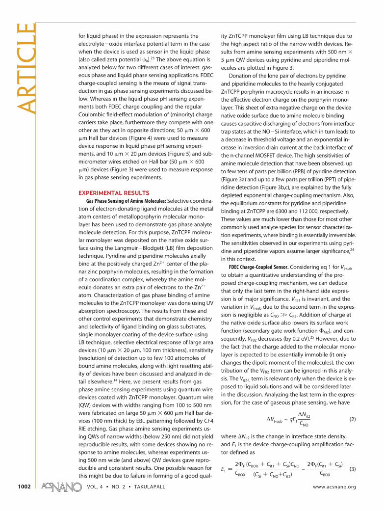
for liquid phase) in the expression represents theelectrolyte�oxide interface potential term in the casewhen the device is used as sensor in the liquid phase(also called zeta potential �0).23 The above equation isanalyzed below for two different cases of interest: gas-eous phase and liquid phase sensing applications. FDECcharge-coupled sensing is the means of signal trans-duction in gas phase sensing experiments discussed be-low. Whereas in the liquid phase pH sensing experi-ments both FDEC charge coupling and the regularCoulombic field-effect modulation of (minority) chargecarriers take place, furthermore they compete with oneother as they act in opposite directions; 50 �m � 600�m Hall bar devices (Figure 4) were used to measuredevice response in liquid phase pH sensing experi-ments, and 10 �m � 20 �m devices (Figure 5) and sub-micrometer wires etched on Hall bar (50 �m � 600�m) devices (Figure 3) were used to measure responsein gas phase sensing experiments.
EXPERIMENTAL RESULTSGas Phase Sensing of Amine Molecules: Selective coordina-
tion of electron-donating ligand molecules at the metalatom centers of metalloporphyrin molecular mono-layer has been used to demonstrate gas phase analytemolecule detection. For this purpose, ZnTCPP molecu-lar monolayer was deposited on the native oxide sur-face using the Langmuir�Blodgett (LB) film depositiontechnique. Pyridine and piperidine molecules axiallybind at the positively charged Zn2� center of the pla-nar zinc porphyrin molecules, resulting in the formationof a coordination complex, whereby the amine mol-ecule donates an extra pair of electrons to the Zn2�
atom. Characterization of gas phase binding of aminemolecules to the ZnTCPP monolayer was done using UVabsorption spectroscopy. The results from these andother control experiments that demonstrate chemistryand selectivity of ligand binding on glass substrates,single monolayer coating of the device surface usingLB technique, selective electrical response of large areadevices (10 �m � 20 �m, 100 nm thickness), sensitivity(resolution) of detection up to few 100 attomoles ofbound amine molecules, along with light resetting abil-ity of devices have been discussed and analyzed in de-tail elsewhere.14 Here, we present results from gasphase amine sensing experiments using quantum wiredevices coated with ZnTCPP monolayer. Quantum wire(QW) devices with widths ranging from 100 to 500 nmwere fabricated on large 50 �m � 600 �m Hall bar de-vices (100 nm thick) by EBL patterning followed by CF4RIE etching. Gas phase amine sensing experiments us-ing QWs of narrow widths (below 250 nm) did not yieldreproducible results, with some devices showing no re-sponse to amine molecules, whereas experiments us-ing 500 nm wide (and above) QW devices gave repro-ducible and consistent results. One possible reason forthis might be due to failure in forming of a good qual-
ity ZnTCPP monolayer film using LB technique due to
the high aspect ratio of the narrow width devices. Re-
sults from amine sensing experiments with 500 nm �
5 �m QW devices using pyridine and piperidine mol-
ecules are plotted in Figure 3.
Donation of the lone pair of electrons by pyridine
and piperidine molecules to the heavily conjugated
ZnTCPP porphyrin macrocycle results in an increase in
the effective electron charge on the porphyrin mono-
layer. This sheet of extra negative charge on the device
native oxide surface due to amine molecule binding
causes capacitive discharging of electrons from interface
trap states at the NO�Si interface, which in turn leads to
a decrease in threshold voltage and an exponential in-
crease in inversion drain current at the back interface of
the n-channel MOSFET device. The high sensitivities of
amine molecule detection that have been observed, up
to few tens of parts per billion (PPB) of pyridine detection
(Figure 3a) and up to a few parts per trillion (PPT) of pipe-
ridine detection (Figure 3b,c), are explained by the fully
depleted exponential charge-coupling mechanism. Also,
the equilibrium constants for pyridine and piperidine
binding at ZnTCPP are 6300 and 112 000, respectively.
These values are much lower than those for most other
commonly used analyte species for sensor characteriza-
tion experiments, where binding is essentially irreversible.
The sensitivities observed in our experiments using pyri-
dine and piperidine vapors assume larger significance,24
in this context.
FDEC Charge-Coupled Sensor. Considering eq 1 for Vt-sub
to obtain a quantitative understanding of the pro-
posed charge-coupling mechanism, we can deduce
that only the last term in the right-hand side expres-
sion is of major significance. VFB1 is invariant, and the
variation in Vt-sub due to the second term in the expres-
sion is negligible as CNO Cit2. Addition of charge at
the native oxide surface also lowers its surface work
function (secondary gate work function M2), and con-
sequently, VFB2 decreases (by 0.2 eV).25 However, due to
the fact that the charge added to the molecular mono-
layer is expected to be essentially immobile (it only
changes the dipole moment of the molecules), the con-
tribution of the VFB2 term can be ignored in this analy-
sis. The Vg2-L term is relevant only when the device is ex-
posed to liquid solutions and will be considered later
in the discussion. Analyzing the last term in the expres-
sion, for the case of gaseous phase sensing, we have
where �Nit2 is the change in interface state density,
and E1 is the device charge-coupling amplification fac-
tor defined as
∆Vt-sub ∼ qE1
∆Nit2
CNO(2)
E1 )2ΦF
CBOX
(CBOX + Cit1 + CSi)CNO
(CSi + CNO+Cit2)∼
2ΦF(Cit1 + CSi)
CBOX(3)
ART
ICLE
VOL. 4 ▪ NO. 2 ▪ TAKULAPALLI www.acsnano.org1002

To get a rough estimate of the numbers, in our
case of boron-doped (1015 cm�3, F � 0.3 eV) thin film
silicon (100 nm) SOI MOSFET with 400 nm thick BOX
and approximate interface state density (assumed) of 5
� 1011 cm�2 at the Si�BOX interface, amplification fac-
tor is calculated to be E1 � 13. If �Nit2 � 1 � 1012 cm�2
and CNO � 17.2 � 10�7 F cm�2, (q�Nit2/CNO) � 0.093.
Hence, the shift in threshold voltage of the inversion
channel formed at the Si�BOX interface is �Vt-sub � 1.2
V. When the surface of a fully depleted device biased
in weak inversion (subthreshold region) is exposed to
ligand molecules, as in the amine sensing experiments,
added negative charge at the native oxide surface
causes amplified modulation of device threshold volt-
age and drives it into strong inversion regime, result-
ing in an exponential gain in drain current response by
a factor of 10 or more. This unique exponential coupling
of the device response to the surface charge imparted
by the target species in a monolayer floating gate, fully
depleted SOI MOSFET leads to terming of the device
structure as a fully depleted exponentially coupled
(FDEC) sensor.
Liquid Phase pH Sensing. The delineation between regu-
lar MOSFET (inversion)-type field-effect response,
termed “Coulombic” response hereafter, and the pro-
posed FDEC response become apparent when the de-
vice with bare native oxide is exposed to aqueous
buffer solutions of varying pH. The active surface (50
Figure 3. (a) Response of a 500 nm wide device coated with ZnTCPP. Saturated pyridine vapor was diluted 105 times with nitro-gen, and 10 mL amount of this was introduced into Teflon cell enclosing the device. Device response to two aliquots introduced10 min apart is shown. The vertical drop in drain current due to device resetting using LED light incidence and nitrogen purgeis explained in ref 14. Inset shows FESEM image of a 500 nm device. (b) Response of 500 nm wide device to piperidine vapor di-luted 107 times with nitrogen (red curve). Device does not exhibit any significant response to pure nitrogen (control), plotted inblue. The large response of device relative to the plot in (a) is understood to be due to higher binding constant and larger basestrength of piperidine compared to pyridine. Inset shows picture of 50 mL internal volume Teflon cell assembly (cap off) with wirebonded device, integrated inside a HP test fixture. (c) Response of 500 nm wide device to piperidine vapor diluted 109 timeswith nitrogen (red curve). Two 10 mL aliquots of 6 PPT vapor, followed by pure nitrogen and 60 PPT vapor (108 times diluted)are introduced. A detailed study of amine sensing is discussed elsewhere.14
ARTIC
LE
www.acsnano.org VOL. 4 ▪ NO. 2 ▪ 999–1011 ▪ 2010 1003

�m wide � 600 �m long) of a well-packaged device
was treated with buffered oxide etch, dried in nitrogen,
and fresh native oxide was grown in clean-room ambi-
ent conditions.26 Threshold voltage of the device was
defined arbitrarily in these experiments as the substrate
bias corresponding to an inversion drain current of 10
nA. Device native oxide surface was exposed to differ-
ent pH buffer solutions, and threshold voltage was
measured with time by maintaining the drain current
constant at 10 nA while varying the substrate bias (gate
voltage) using a feedback circuit. Threshold voltage
variation with time as the device is exposed to differ-
ent pH buffer solutions is plotted in Figure 4a.
In typical FET-based sensor structures, a gradual (lin-
ear or nonlinear) unidirectional variation in threshold
voltage is observed going from pH 11 to pH 3,5,7,10
which in the case of n-channel MOSFET sensors is a
gradual decrease in the threshold voltage, or equiva-
lently decrease in sheet resistance. Whereas, in our ex-
periments when using the FDEC sensor, the device ex-
hibits anomalous shifts at two pH transition points. In
Figure 4a at pH 8�7 and pH 11�10, the direction of
Figure 4. (a) Well encapsulated 50 �m � 600 �m Hall bar device with a 150 �m � 450 �m SU8 window (inset) is exposed to pHbuffer solutions. Measured threshold voltage variation of the device with pH value of solution is plotted vs time. Data labels in theplot are pH values. The device exhibits anomalous shifts transitioning from pH 8 to pH 7 and from pH 11 to pH 10, where the thresh-old voltage increases, in opposite direction compared to other pH transitions. (b) Threshold voltage variation plotted against pHvalue of buffer solution for four different devices. All devices exhibit anomalous responses when transitioning from pH 8 to pH 7and from pH 11 to pH 10. In the inset is plotted device threshold voltage response vs time when the device is exposed alternatelyto pH 7 and pH 8 (also pH 9) buffer solutions. The anomalous response is seen both ways, from acidic to basic solutions and viceversa. (c) Schematic of single (vicinal) silanol and double silanol (geminal) groups on native oxide surface, and formation of nega-tive charge on oxide surface at anomalous pH points.
ART
ICLE
VOL. 4 ▪ NO. 2 ▪ TAKULAPALLI www.acsnano.org1004

threshold voltage shifts at these transition points is op-posite to the rest of the data and various reports in lit-erature. The anomalous shifts at these two transitionpoints occurred both ways (inset in Figure 4b), whengoing from buffer solutions with lower pH values(acidic) to higher pH values (basic) and vice versa. Thisanomalous behavior has been observed consistently inall experiments using at least six different devices.Threshold voltage variations with pH of buffer solu-tions from experiments using four different devices areplotted in Figure 4b. We initially attributed theseanomalies as errors due to imperfections in the experi-mental setup. Even though the observed nonlinearity inresponse can be explained by considering chemical oxi-dation and reduction of the hydroxyl-terminated na-tive oxide surface,27,28 the anomalies at pH 7�8 and pH10�11 cannot be explained by any of these well-understood and established concepts. In the discus-sion below, device threshold voltage variation with re-spect to increase in pH values of buffer solutions, that is,going from acidic to basic solutions, is analyzed forsake of convenience.
The observed anomalous threshold voltage responsecan be understood as the cumulative of two different, op-positely acting effects on the inversion channel carriers:the Coulombic effect due to electrolyte�native oxide in-terface potential (Vg2-L � �0 in eq 1) and the proposedFDEC effect due to charge addition to the native oxidesurface. The Coulombic effect in a regular MOSFET-typesensor is a function of �0
29 and produces an increase inthreshold voltage of electron inversion channel with de-crease in [H�] ion concentration of the solution, from pH2 to pH 12. It is explained using the site binding30 and thesite dissociation models.31
To explain the FDEC charge-coupling effect, weneed to consider the surface terminal groups on the de-vice native oxide surface and the corresponding sur-face charge due to their reactivity in pH buffer solu-tions. The native oxide formed on the active siliconsurface is known to have various different terminatingmolecular groups, viz. single silanol ('SiOH) groups(isolated and vicinal ends), double silanol groupsASi(OH)2 (germinal ends) and'Si�O�Si' bridgebonds.32 When exposed to basic buffer solutions, theSiOH ends are deprotonated to form SiO� ion-terminated ends, depending on the pH value of thebuffer solution. The cumulative density of these sur-face hydroxyl groups is expected to depend on the sur-face preparation method and has been reported tovary from 0.8 to 8 groups per nm�2,33 with a majorityof them being single silanol groups. The dissociationconstant for deprotonation of single silanol groups ispKa � 7 (reports range from 6.5 to 7.5) and for deproto-nation of the second OH group on double silanol(ASiO�OH) is pKa � 9.8 (reports range from 9.3 to 10),approximately.34�36 Hence, at the two anomalous tran-sition points (pH 7�8 and pH 10�11), changing of
buffer solution to higher basic strength results in largeincreases in negative charge terminations at the nativeoxide surface (Figure 4c),37 along with a correspondingdecrease in Vg2-L.38 This net increase in negative chargeterminations at the native oxide surface (immobilecharge, as defined by electrical double layer and triplelayer models for electrolyte�solid interfaces) mirrors anincrease in positive charge at the NO�Si film interfacedue to the high capacitance of native oxide, resulting inloss of electrons from the interface trap states andhence decrease in device threshold voltage. At thesame time, the corresponding decrease inelectrolyte�NO interface potential (Vg2-L) causes an in-crease in threshold voltage due to Coulombic depletionof charge carriers (electrons) far inside the silicon chan-nel. The net result is cumulative of the two competing ef-fects: the decrease in Vg2-L that tends to cause an in-crease in threshold voltage (Coulombic effect) versusthe FDEC effect due to increased negative charge onthe oxide surface that tends to produce a decrease inthreshold voltage.
In contrast, when the native oxide surface was func-tionalized with aminopropyltriethoxysilane (APTES)molecules, the anomalies in threshold voltage responsewere not observed,27 similar to linear versus nonlinearpH response of nanowire devices reported by Cui et al.5
APTES molecule binding consumes most of the surfacesilanol groups, resulting in no observed FDEC capacitivecharge coupling. However, the amine end (pKa � 9.5)of the APTES molecules is free to undergo proton ex-change, but the net charge formed at the amine endsdoes not show any explicit FDEC-type threshold voltagedecrease. This may be due to the screening of thischarge by the solvent molecules along with the re-duced capacitance in this case between charges at theamine ends and interface states at the NO�Si interface.
Liquid Phase Analytical Model, FDEC Potential Coupling. Whileevaluating the sensing response of the device in the liq-uid phase, the Vg2-L term in eq 1 for Vt-sub needs to betaken into account. The Vg2-L term denotes theelectrolyte�insulator interface potential �0 (zeta poten-tial) in this configuration.29 In a fully depleted field-effect sensor structure, even the Coulombic field-effectmodulation of channel carriers by theelectrolyte�oxide interface potential Vg2-L is amplifiedexponentially when compared to a partially depleteddevice structure. Elibol et al. have reported a similaranalysis using a double gated thin film SOI FET struc-ture.39 In our case of n-channel FDEC sensor structure,threshold voltage variation with electrolyte�oxide in-terface potential can be written as
tSiOH 798pH 7 T pH 8
tSiO- + H+
dSiO-(OH) 798pH 10 T pH 11
) SiO22- + H+
ARTIC
LE
www.acsnano.org VOL. 4 ▪ NO. 2 ▪ 999–1011 ▪ 2010 1005

where the amplification factor for electrolyte�oxide in-
terface potential E2 is given by
The amplification factor is negative in the above
equation because a decrease in Vg2-L (�0) produces an
increase in Vt-sub. Also to be noted is that E2 is relatively
independent of interface trap state densities. Using the
device parameters, E2 for our device can be calculated
to be �12. For pH buffer solutions, the
electrolyte�oxide interface potential (zeta potential)
changes by a theoretical maximum of 0.059 V per unit
change in pH at 298 K.23 This translates to a maximum
device threshold voltage variation of �Vt-sub � 0.7 V per
unit pH change due to amplification, for our FDEC de-
vice. This amplified response may explain the large am-
plitude changes in threshold voltage transitioning from
pH 6 to pH 7 in our experiments, compared to reports
of similar experiments with other structures.
Additionally, referring to eq 1 for Vt-sub, since �VFB2
� �M2, where M2 is the work function of a chemical
sensitive thin film deposited on the active surface of the
device, the device can also be used to sense work func-
tion changes caused by target molecule interactions.40
This is the case when a decrease in M2 is accompanied
by formation of free charge carriers (electrons that are
mobile) in the chemical sensitive film, where electron
transfers occur from the chemical-sensitive film to the
fully depleted silicon, resulting in energy bands bend-
ing downward in the silicon film causing a flush of ex-
tra electrons in the channel (similar to functioning of a
MESFET) and hence resulting in a decrease in the
threshold voltage of inversion channel (“MESFET”-type
response, hereafter). In our gas phase amine binding ex-
periments, work function of the porphyrin monolayer
decreases but is accompanied only by a change in di-
pole moment of the porphyrin molecules
(porphyrin�amine coordination complex). There is no
free charge on the porphyrin monolayer due to amine
binding, hence we do not expect any substantial contri-
bution due to the MESFET-type effect. Therefore, FDEC
charge-coupling effect due to capacitive interface state
coupling (as explained previously) is expected to be
the main cause of the observed gas phase amine bind-
ing response.
From eq 1, it can be deduced that the fully de-
pleted device amplification factor for MESFET-type re-
sponse is �E2 � (Csi/CBOX), as a decrease in M2 results
in a decrease in Vt-sub. However, the presence of inter-
face trap states at the NO�Si interface reduces the sen-
sitivity of device to free charge addition on the
chemical-sensitive film. Hence, interface trap states
and other defects need to be reduced when the de-
vice is used as a sensor in this MESFET-type configura-
tion to avoid secondary effects.
Cumulative change in substrate threshold voltage
(�Vt-sub) due to all the different contributions can hence
be written as
Numerical Simulations. To further understand and vali-
date the concepts and the theoretical framework pre-
sented above, we modeled the working of the device
using Atlas numerical simulations software (Silvaco
Corp). Owing to the complex nature of interactions at
the various interfaces of the sensor device and within
the inverted silicon channel, caused by target molecule
binding at the chemical-sensitive film in such hybrid
semiconductor device structures with
organic�inorganic interfaces, and the relative high
level of difficulty in exact modeling of these, we have
developed a simplified model that represents these
complex interactions using the modeling tools avail-
able in Atlas device simulation software. We present
here a simple model, an alternative model to the one
we previously presented,14 that simulates the capacitive
charge coupling, potential coupling, and the work func-
tion coupling interactions within the MOSFET sensor
device and validates the FDEC theory to explain the re-
sults obtained in our experiments. This simplistic model
extended here is to be viewed in terms of a proof of
concept, validating and enabling understanding of the
sensing mechanisms delineated above. A more exact
simulation model involving molecular orbital coupling
with interface states and the energy band levels in sili-
con needs to be developed to better understand the
device physics41 and forms part of the future work.
A SOI MOSFET device (Figure 5) of 10 �m length, 100
nm channel thickness, and 1 �m width controlled by
substrate silicon acting as gate was defined using the
simulation parameters listed in Table 1. The native ox-
ide layer is modeled as a 2 nm thick thermal oxide on
the silicon channel region, and the ZnTCPP porphyrin
monolayer is modeled by defining a 2 nm thin semicon-
ducting layer (with parameters similar to intrinsic sili-
con) on top of the native oxide, while isolated from the
source�drain regions at either ends (by 100 nm) to
avoid conductance through the 2 nm film. The use of
a semiconducting thin film to model ZnTCPP mono-
layer is due to the reported semiconducting nature of
porphyrin molecules in both thin film and bulk solid
phases.42,43 Interface trap states are defined separately
at each of the two interfaces, above and below the sili-
con channel, using Gaussian profiles as plotted in Figure
5a. Lower fixed oxide charge density value at the
NO�SOI interface is used in order to optimize the simu-
lated FDEC response. Also donor states at the NO�SOI
interface above the Fermi level act equivalent to fixed
∆Vt-sub ∼ E2∆Vg2-L (4)
E2 ) -CNOCSi
CBOX(CSi + CNO+Cit2)∼ -
CSi
CBOX(5)
∆Vt-sub ∼ qE1
∆Nit2
CNO+ E2(∆Vg2-L - ∆ΦM2) (6)
ART
ICLE
VOL. 4 ▪ NO. 2 ▪ TAKULAPALLI www.acsnano.org1006

oxide charges. A drain current versus (substrate) gate
bias characteristic curve (blue curve in Figure 5c) be-
fore binding of the target molecules onto the chemical
sensitive film, similar to that measured in our experi-
ment (inset Figure 5c, blue curve), is obtained by vary-
ing the fitting parameters listed in Table 1.
As discussed in the previous sections, amine mol-
ecule binding at the ZnTCPP porphyrin monolayer
causes an effective increase in the negative charge on
the porphyrin monolayer, producing a resultant in-
crease in (electron) inversion channel current. In our
simulations, this effective increase in negative charge
due to target molecule binding events is modeled by
the addition of excess “negative fixed oxide charge” at the
model monolayer�native oxide interface, whereby this
negative fixed oxide charge added on top of the native
oxide is capacitively coupled with the interface trap
states at the native oxide�silicon channel interface,
simulating the proposed FDEC charge-coupling mecha-
nism. Negative fixed oxide charge is used to simulate
the negative charge on molecular monolayer due to the
immobile nature of the fixed oxide charge, compared
to simulating it by changing the work function of the
model porphyrin semiconducting thin film (or a float-
Figure 5. (a) On the top is plotted interface state density profile defined at the top oxide (NO)�Si interface. Donor-type trap states areused as they are expected to interact (FDEC) most below the Fermi level in our boron-doped SOI. Below is plotted donor and acceptorstate profiles defined at the Si�BOX interface. (b) Two-dimensional electron density distribution (Tonyplot, Atlas) plot with no charge(left) defined at the 2 nm model porphyrin semiconducting film�top oxide (NO) interface, and with �3 � 1010 cm�2 fixed oxide chargedefined at the interface (right). Addition of negative fixed oxide charge simulates the amine molecule binding at ZnTCPP monolayer inour experiments. Red color in the plot corresponds to electron density of 1018 cm�3, and pink color to 103 cm�3. As can be seen, addi-tion of charge on the top oxide induces inversion at the Si back channel �1012 cm�2, an order of magnitude higher charge density rela-tive to negative fixed oxide charge added on top. (c) Numerically simulated Id�Vg curves for varying negative fixed oxide charge densi-ties added at the model porphyrin film�top oxide (NO) interface. Data labels are density per cm2. Experimental drain current curvesbefore (blue) and after (red) pyridine binding at ZnTCPP monolayer (ref 14) are plotted in the inset. Drain current crossover going fromdepletion to inversion, and corresponding decrease in threshold voltage can be seen. These characteristics are reproduced in the nu-merical simulations. (d) Numerically simulated threshold voltage variation plotted against negative fixed oxide charge density. Log ofionized donor trap density at the top oxide�Si interface is plotted on the secondary y-axis. (e) Numerically simulated threshold volt-age variation with change in floating gate (defined at the model porphyrin film�top oxide interface) work function and potential (sec-ondary x-axis). Work function variation with high (1013 cm�2 eV�1) and low (1012 cm�2 eV�1) interface state density, at the top oxide�NOinterface is plotted. Slope of linear fit(s) agrees well with the rough estimate of E2 obtained in the previous section.
ARTIC
LE
www.acsnano.org VOL. 4 ▪ NO. 2 ▪ 999–1011 ▪ 2010 1007

ing gate) where transfer of charge carriers invariably oc-
curs. For this reason, to improve the effectiveness of
simulating charge coupling using negative fixed oxide
charge to model target molecule binding, electronic
band parameters of the 2 nm thick model porphyrin
semiconducting thin film are defined such that the in-
teractions between the carriers and energy states inside
the 2 nm thin film, with the interface states and the
charge carriers in the silicon channel are minimized
(electron affinity of 4.9, and density of states (DOS) at
300 K of 1014, in both valence and conduction bands).
By incrementally increasing the negative fixed ox-
ide charge density defined at the model
monolayer�native oxide interface, representing
gradual amine molecular binding with time at the
ZnTCPP chemical sensitive monolayer, back channel
drain current versus (substrate) gate bias curves for
drain�source bias of 0.1 V are numerically simulated,
while keeping all other parameters constant. It is to be
noted that amine molecule binding at the ZnTCPP mol-
ecule is expected to form an electrical dipole on the
amine�ZnTCPP coordination complex, with partial
charge polarization of either moieties. The charge simu-
lated here by defining the negative fixed oxide charge
is the cumulative of these partial charge densities on
the molecular monolayer. Hence, any defined negative
fixed oxide charge density might correspond to as
much as a 10-fold target (amine) molecule binding den-
sity at the chemical-sensitive device surface. Numeri-
cally simulated drain current curves for negative fixed
oxide charge density values ranging from 109 to 1012
cm�2 are plotted in Figure 5c.
Threshold voltage shifts of the simulated curves
from the initial (threshold voltage corresponding to no
binding of target amine molecules) are plotted in Fig-ure 5d against the negative fixed oxide charge definedat the model monolayer�native oxide interface. In thesame figure on the secondary y-axis is plotted the cu-mulative positive charge due to charging and discharg-ing of interface states at the native oxide�silicon chan-nel interface (at initialization, zero bias condition),caused by the capacitive coupling of these interfacestates with the negative fixed oxide charge added atthe simulated monolayer�native oxide interface. Ascan be seen from plot in Figure 5d, the decrease insimulated threshold voltage with increase in negativefixed oxide charge is not a monotonous function. Thismay be due to the complex nature of interactions be-tween the added negative fixed oxide charges, inter-face trap states defined at the top oxide�silicon chan-nel interface, valence and conduction band states in themodel semiconducting porphyrin layer, the electronstates in silicon channel, etc. and the resulting inaccura-cies associated with the initialization and convergenceof numerical simulations. It can be seen that addition of�3 � 1010 cm�2 fixed oxide charge produces over 3 or-ders of magnitude increase in drain current when bi-ased in weak inversion regime. This corresponds to adensity of fewer than two charges per 100 nm2 area, oran order of magnitude increase in drain current corre-sponds to less than two charges per 1 �m2 area. Hence,a 10 �m length � 100 nm width nanowire FDEC de-vice is expected to detect unit charge additions, targetbinding events on the device surface, with up to an or-der of magnitude increases in device drain current.
A linear fit of simulated data (excluding last datapoint) yields a threshold voltage lowering of 0.23 V per1 order increase in negative fixed oxide charge densityfor the set of parameters listed in Table 1, provided theminimum fixed charge density defined is within a feworders of that corresponding to the ionized interfaceand surface states (to avoid charge screening). As thenegative fixed charge density is increased further,above 1011 cm�2, the simulated threshold voltage ofthe device begins to increase. This is expected to oc-cur when Coulombic effect due to added negative fixedoxide charge offsets the FDEC effect due to interfacestate charge coupling, when the effective capacitanceacross the top oxide (NO) due to interface trap statesfalls low compared to the increased negative fixed ox-ide charge density, whereby the latter directly modu-lates the inversion charge density at the BOX�Siinterface.
Comparing the measured device Id�Vg curves be-fore and after exposure to amine molecules, the experi-mental data plotted in the inset of Figure 5c, we ob-serve that the curves exhibit a crossover at 3 V substrategate bias. This crossover point is expected to occurwhen conductance in the Si channel transitions fromdepletion regime to inversion regime, with inversionchannel formed at the BOX�Si channel interface, fur-
TABLE 1. Numerical Simulation Parameters Used forModeling the Fully Depleted SOI FET Device Using AtlasSoftware (Silvaco Corp)
atlas simulation parameter value
SOI channel thickness 100 nmSOI device, length � width 10 �m � 1 �mburied oxide thickness 400 nmSOI channel doping p-type (boron), 1015 cm�3
model porphyrin semiconducting film (2 nm)electron affinity 4.9 eVDOSa at 300 K (in valence and conduction bands) 1014
fixed oxide charge densityat SOI channel-native oxide interface 1 � 108 cm�2
at SOI channel-buried oxide interface 1 � 109 cm�2
at buried oxide-silicon substrate interface 1 � 1011 cm�2
interface trap density, Nit
at SOI channel�native oxide interface 1 � 1013 cm�2
(EV�EGDb � 0.35, 25 degenerate levels) (donors, Gaussian profile)
at SOI channel�buried oxide interface 2 � 1011 cm�2
(EV�EGDb � 0.35, EC�EGA � 0.35, 25 levels) (equal donors and acceptors,
Gaussian profile)
aDOS, density of states. bEv, valence band energy; EGD, peak energy of Gaussianprofile.
ART
ICLE
VOL. 4 ▪ NO. 2 ▪ TAKULAPALLI www.acsnano.org1008
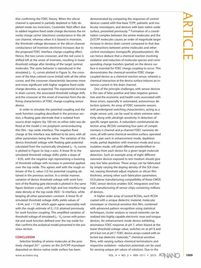
ther confirming the FDEC theory. When the siliconchannel is operated in partially depleted or fully de-pleted mode (no inversion), Coulombic field effect dueto added negative fixed oxide charge decreases the mi-nority charge carrier (electrons) conductance in the sili-con channel, whereas when it is biased in inversion,the threshold voltage decreases or the silicon channelconductance (of inversion electrons) increases due tothe proposed FDEC interface charge-coupling effect.Hence, the two curves crossover, and the red curve isshifted left at the onset of inversion, resulting in lowerthreshold voltage after binding of the target (amine)molecules. The same behavior is reproduced in thesimulated Id�Vg curves plotted in Figure 5c, the cross-over of the blue colored curve (initial) with all the othercurves, and the crossover characteristic becomes moreand more significant with higher negative fixed oxidecharge densities, as expected. The exponential increasein drain current, the associated threshold voltage shift,and the crossover at the onset of inversion form the de-fining characteristics of FDEC charge-coupling sensordevice.
In order to simulate the potential coupling and thework function coupling described in the previous sec-tion, a floating gate electrode that is isolated fromsource drain regions (by 100 nm on either side) was de-fined at the model 2 nm porphyrin semiconductingthin film�top oxide interface. The negative fixedcharge at the interface was defined to be zero, with allother parameters being the same. The variation of thedevice threshold voltage with floating gate potentialcalculated from the numerically simulated Id�Vg curvesis plotted in Figure 5e (top x-axis). A linear fit to thesimulated threshold voltage shifts yields a slope of�8.95, with the negative sign representing a loweringof threshold voltage with increase in potential appliedover the top oxide. This agrees well with the rough es-timate of the E2 value (12) for potential coupling ob-tained in the previous section. In a similar manner,variation of device threshold voltage with work func-tion of the floating gate electrode is plotted in the samefigure (bottom x-axis), with high and low interface trapstate density at the top oxide (NO)�Si interface, whilekeeping all other parameters constant. A linear fit ofsimulated threshold voltage shifts yields values of�8.44, and �11.84, which again agree reasonably wellwith the rough estimate of E2 (12) attained previouslyfor work function coupling. This amplified variation ofthreshold voltage of simulated Id�Vg curves with poten-tial and work function defined over the top oxide fur-ther confirms the analytical model presented in the pre-vious section.
CONCLUSIONSelective binding of amine molecules at the posi-
tively charged Zn2� centers on the ZnTCPP monolayerdeposited on device native oxide surface has been
demonstrated by comparing the responses of controldevices coated with free-base TCPP, palmetic acid mo-lecular monolayers, and devices with bare native oxidesurface, presented previously.14 Formation of a coordi-nation complex between the amine molecules and theZnTCPP molecules causes an order of magnitude largerincrease in device drain current compared to that dueto interactions between amine molecules and othercontrol monolayers (nonspecific physiadsorption). Wecan hence deduce that a chemical reaction involvingoxidation and reduction of molecular species and corre-sponding charge transfers (partial) on the device sur-face is essential for FDEC charge coupling to occur. Thisdemonstrates the chemical-sensitive FDEC charge-coupled device as a chemical reaction sensor, wherein achemical interaction at the device surface induces an in-version current in the drain channel.
One of the principle challenges with sensor devicesis the rate of false positive and false negative genera-tion and the economic and health costs associated withthese errors, especially in automated, autonomous de-tection systems. An array of FDEC nanowire sensorswith predesigned switching characteristics, acting as asingle sensor unit, can be used to attain extreme selec-tivity along with ultrahigh sensitivity in detection ofspecific target species. A redundant combinatorial de-tection array (RCDA) containing four pairs of comple-mentary n-channel and p-channel FDEC nanowire de-vices, all with same chemical-sensitive surface, operatedwith a pair each in enhancement mode, depletionmode, partial depletion with inversion mode and accu-mulation mode, will yield different preidentified re-sponses from each device for a given target moleculedetection. Such an example array of eight differentnanowire devices exposed to test medium should givevery low false positives. These arrays can be fabricatedby simply varying the doping density of the SOI chan-nel, varying threshold adjust implants or silicon filmthickness, among other such fabrication parameters.ULSI planar manufacturing compatibility of these CMOSFDEC sensor devices enables SOC integration and lowcost manufacturing of sensor chips containing millionsof devices.
A higher order array of nested RCDAs, each RCDAcoated with a unique dielectric material, molecularmonolayer or chemical-sensitive thin film, combinedwith advanced pattern recognition using statisticaltechniques, cluster analysis or neural networks can berealized into highly capable electronic nose and tonguedevices. An enhancement mode device exhibitinganomalous FDEC response at pH 7, when biased at thelower threshold voltage value, switches on at pH 8 andpH 6 but not at pH 7. FDEC device arrays coated with se-lected top dielectric materials,35 chemical-sensitivefilms, with varying surface chemical terminations andrespective oxidation�reduction potentials can be usedfor sensing unique pH values of solutions. Due to the
ARTIC
LE
www.acsnano.org VOL. 4 ▪ NO. 2 ▪ 999–1011 ▪ 2010 1009

fact that FDEC charge coupling occurs at specific pHvalue of solution for a given surface chemistry of the de-
vice, these sensor arrays can be used as reference-lesspH sensors.
METHODSDevice Fabrication: Starting material for the back gated SOI
MOSFET transistors used in this work is a p-type SOI wafer (� �2�10 � · cm) with initial SOI film thickness of 200 nm and under-lying buried oxide (BOX) layer thickness of 400 nm, sourcedfrom IBIS Technology Corporation. The SOI channel thickness isthinned to 100 nm by wet oxidation at 1000 °C. Plasma-enhanced chemical vapor deposition (PECVD) is performed tofurther increase the oxide thickness and to obtain an effectiveoxide mask for phosphorus n� doping. Buffered oxide etch(BOE) is used to open windows in the thick oxide layer forsource�drain n� doping. Phosphorus doping is carried out us-ing phosphorus pentoxide solid source wafers in a diffusion fur-nace. The masking oxide is then removed by dipping the wafer inBOE for 15 min. Device isolation is attained by physical separa-tion via reactive ion etching (RIE) of patterned silicon mesas us-ing SF6 etch chemistry. The wafer is then patterned to open win-dows in the buried oxide for deposition of a metal layer to enableelectrical contact to the silicon substrate gate. BOE is used toetch away the buried oxide from the patterned openings. Metalcontacts to substrate and devices are formed by deposition of200 nm of aluminum, using a TorrVac electron beam evapora-tor. Bonding pads are formed by depositing 10 nm of chromiumfollowed by 100 nm gold in an Edwards’s thermal evaporator.Ten micrometer � 20 �m and large 50 �m � 600 �m Hall bardevices were fabricated using these conventional n-MOS processsteps. Submicrometer quantum wire devices from 100 to 500nm wide devices were formed on 50 �m � 600 �m bars by elec-tron beam lithography (EBL) patterning of PMMA resist, fol-lowed by reactive ion etching (RIE) using CF4 etch chemistry.
LB Porphyrin Monolayer Deposition: Zn(II) 5,10,15,20-tetra-(3-carboxylphenyl)porphyrin (ZnTCPP) monolayer deposition bythe Langmuir�Blodgett technique has been done using a con-stant perimeter barrier type Joyce-Loebl Mini LB trough. Twentymicromolar solutions of porphyrin molecules are prepared bydissolving ZnTCPP in 2:1 mixture of dichloromethane andmethanol. Porphyrin monolayers are formed in LB trough overa water subphase with a pH of 4.5, prepared using hydrochloricacid. The deposition of the porphyrin monolayer onto the devicesurface was done by very slow withdrawing of an immersed de-vice, while applying a constant pressure of 20 mN · m�1 on the LBconstant perimeter barrier.
Gas Phase Amine Sensing Experiments: Gas phase amine bindingexperiments were performed inside a custom-built Teflon cell,with inlets and outlets for pumping of analyte gases. Teflon cellwas integrated with white LED for light exposure for device reac-tivation. Dilute amine vapors (pyridine and piperidine) were pre-pared by mixing pure nitrogen gas with saturated amine va-pors formed over nitrogen gas in a conical flask. 0.5 mL ofsaturated amine vapor in a 5 mL disposable syringe was in-jected, mixed into 49.5 mL of pure nitrogen gas in a 50 mL sy-ringe using disposable valve adaptors to yield 100 times dilutedamine vapor. All syringes and valve adaptors were discarded af-ter a single use. A repetition of the above method using newparts yielded 10 000 times diluted amine vapor, and so on. Eachdilution step took about 5 min, much less than few hours’ timescale for significant Brownian particle (molecular) absorptiononto syringe tube walls. The device was illuminated with LEDlight (350 mW/cm2 for 30 min),14 followed by 10 mL aliquots ofdiluted amine vapors introduced into Teflon cell assembly anddevice response measured. A repetition of dilution and mixingprocess with no amine vapor but with just nitrogen gas when in-troduced showed no device response (blue curve in Figure 3b),while diluted pyridine and piperidine vapors showed consistentresponses, that is, progressive lowering of device responses forhigher dilutions and lower base strengths. Vapor pressures of py-ridine (16 mmHg) and piperidine (25 mmHg) at NTP were usedin sensitivity calculations.
Liquid Phase pH Sensing Experiments: For liquid phase experi-ments, device isolation and encapsulation were achieved by us-ing a two-step process. First, 100 �m thick SU8 resist coating wasused to open windows over active area of the device and overbonding pads to enable electric contact with external circuit; 50�m � 600 �m large Hall bar devices were used for pH sensingexperiments due to ease of isolation (inset Figure 4a). The device(die) was glued onto a chip carrier, and electric contacts wereformed by gold wire bonding using ultrasonic ball-wedgebonder. As a second step of encapsulation, 5 min commercial ep-oxy glue was applied to cover bonding pad areas and all otherelectrical contacts to achieve electric insulation when testingwith aqueous pH solutions. Fully encapsulated device with openwindows over active device areas was treated with BOE solu-tion, and fresh native oxide was grown in clean-room condi-tions. The device was inverted surface down, its surface thor-oughly wetted with DI water and immersed into different pHbuffer solutions, and drain current response was measured.
Acknowledgment. The author thanks Professor Trevor Thorn-ton and Professor Devens Gust for helpful discussions, Drs. GezM. Laws, Paul A. Liddell, Joakim Andre’asson, Yuichi Terazono,and Zach Erno for porphyrin monolayer deposition, characteriza-tion, and synthesis. This work was supported partially by the Na-tional Science Foundation, Award Nos. ECS0097434 and CHE-0352599.
REFERENCES AND NOTES1. Schedin, F.; Geim, A. K.; Morozov, S. V.; Hill, E. W.; Blake, P.;
Katsnelson, M. I.; Novoselov, K. S. Detection of IndividualGas Molecules Adsorbed on Graphene. Nat. Mater. 2007, 6,652–655.
2. Armani, A. M.; Kulkarni, R. P.; Fraser, S. E.; Flagan, R. C.;Vahala, K. J. Label-Free, Single-Molecule Detection withOptical Microcavities. Science 2007, 317, 783–787.
3. Kemiktarak, U.; Ndukum, T.; Schwab, K. C.; Ekinci, K. L.Radio-Frequency Scanning Tunnelling Microscopy. Nature2007, 450, 85–88.
4. Kong, J.; Franklin, N. R.; Zhou, C. W.; Chapline, M. G.; Peng,S.; Cho, K. J.; Dai, H. J. Nanotube Molecular Wires asChemical Sensors. Science 2000, 287, 622–625.
5. Cui, Y.; Wei, Q. Q.; Park, H. K.; Lieber, C. M. NanowireNanosensors for Highly Sensitive and Selective Detectionof Biological and Chemical Species. Science 2001, 293,1289–1292.
6. Forzani, E. S.; Zhang, H. Q.; Nagahara, L. A.; Amlani, I.; Tsui,R.; Tao, N. J. A Conducting Polymer Nanojunction Sensorfor Glucose Detection. Nano Lett. 2004, 4, 1785–1788.
7. Stern, E.; Klemic, J. F.; Routenberg, D. A.; Wyrembak, P. N.;Turner-Evans, D. B.; Hamilton, A. D.; LaVan, D. A.; Fahmy,T. M.; Reed, M. A. Label-Free Immunodetection withCMOS-Compatible Semiconducting Nanowires. Nature2007, 445, 519–522.
8. Sysoev, V. V.; Button, B. K.; Wepsiec, K.; Dmitriev, S.;Kolmakov, A. Toward the Nanoscopic “Electronic Nose”:Hydrogen vs Carbon Monoxide Discrimination with anArray of Individual Metal Oxide Nano- and MesowireSensors. Nano Lett. 2006, 6, 1584–1588.
9. Bergveld, P. Thirty years of ISFETOLOGY: What Happenedin the Past 30 Years and What May Happen in the Next 30Years. Sens. Actuators, B 2003, 88, 1–20.
10. Nikolaides, M. G.; Rauschenbach, S.; Bausch, A. R.Characterization of A Silicon-on-Insulator Based Thin FilmResistor in Electrolyte Solutions for Sensor Applications.J. Appl. Phys. 2004, 95, 3811–3815.
ART
ICLE
VOL. 4 ▪ NO. 2 ▪ TAKULAPALLI www.acsnano.org1010

11. He, T.; Corley, D. A.; Lu, M.; Spigna, N. H. D.; He, J.;Nackashi, D. P.; Franzon, P. D.; Tour, J. M. ControllableMolecular Modulation of Conductivity in Silicon-BasedDevices. J. Am. Chem. Soc. 2009, 131, 10023–10030.
12. Colinge, J.-P. Silicon-On-Insulator Technology: Materials toVLSI, 3rd ed.; Springer: Berlin, 2005.
13. Celler, G. K.; Cristoloveanu, S. Frontiers of Silicon-on-Insulator. J. Appl. Phys. 2003, 93, 4955–4978.
14. Takulapalli, B. R.; Laws, G. M.; Liddell, P. A.; Andreasson, J.;Erno, Z.; Gust, D.; Thornton, T. J. Electrical Detection ofAmine Ligation to a Metalloporphyrin via a Hybrid SOI-MOSFET. J. Am. Chem. Soc. 2008, 130, 2226–2233.
15. Schroder, D. K.; Babcock, J. A. Negative Bias TemperatureInstability: Road to Cross in Deep Submicron SiliconSemiconductor Manufacturing. J. Appl. Phys. 2003, 94, 1–18.
16. Ogawa, S.; Shimaya, M.; Shiono, N. Interface-TrapGeneration at Ultrathin SiO2 (4�6nm)�Si InterfacesDuring Negative-Bias Temperature Aging. J. Appl. Phys.1995, 77, 1137–1148.
17. Stesmans, A. Low-Temperature Electron-Spin-ResonanceStudy of Pb0 Defects Residing in the (111) Si/Native OxideInterface. Appl. Surf. Sci. 1987, 30, 134–141.
18. Stesmans, A. Structural Relaxation of Pb Defects at the(111)Si/SiO2 Interface as a Function of OxidationTemperatureOThe Pb-Generation-Stress Relationship.Phys. Rev. B 1993, 48, 2418–2435.
19. Poindexter, E. H.; Caplan, P. J.; Deal, B. E.; Razouk, R. R.Interface States and Electron-Spin Resonance Centers inThermally Oxidized (111) and (100) Silicon-Wafers. J. Appl.Phys. 1981, 52, 879–884.
20. Balestra, F.; Brini, J.; Gentil, P. Deep Depleted SOI MOSFETswith Back Potential ControlOA Numerical-Simulation.Solid-State Electron. 1985, 28, 1031–1037.
21. Hovel, H. J. Si Film Electrical Characterization in SOISubstrates by the HgFET Technique. Solid-State Electron.2003, 47, 1311–1333.
22. Balestra, F.; Benachir, M.; Brini, J.; Ghibaudo, G. AnalyticalModels of Subthreshold Swing and Threshold Voltage forThin-Film and Ultra-Thin-Film SOI MOSFETs. IEEE Trans.Electron Dev. 1990, 37, 2303–2311.
23. Olthuis, W. Chemical and Physical FET-Based Sensors orVariations on an Equation. Sens. Actuators, B 2005, 105,96–103.
24. Dan, Y.; Lu, Y.; Kybert, N. J.; Luo, Z.; Johnson, A. T. C.Intrinsic Response of Graphene Vapor Sensors. Nano Lett.2009, 9, 1472–1475.
25. Grover, R.; Carthy, B. M.; Zhao, Y.; Jabbour, G. E.; Sarid, D.;Laws, G. M.; Takulapalli, B. R.; Thornton, T. J.; Gust, D.Kelvin Probe Force Microscopy as a Tool for CharacterizingChemical Sensors. Appl. Phys. Lett. 2004, 85, 3926–3928.
26. Ashcroft, B.; Takulapalli, B.; Yang, J.; Laws, G. M.; Zhang,H. Q.; Tao, N. J.; Lindsay, S.; Gust, D.; Thornton, T. J.Calibration of a pH Sensitive Buried Channel Silicon-on-Insulator MOSFET for Sensor Applications. Phys. StatusSolidi B 2004, 241, 2291–2296.
27. Takulapalli, B. R.; Thornton T. J. Gust; D. Ashcroft; B.Lindsay; S. M. Zhang; H. Q.; Tao, N. The pH Response of aSilicon-on-Insulator MOSFET with an IntegratedNanofluidic Cell. SOI Conference, IEEE International, 2003;pp 114�116.
28. Allen, L. H.; Matijevi, E; Meties, L. Exchange of Na� forSilanolic Protons of Silica. J. Inorg. Nucl. Chem. 1971, 33,1293–1299.
29. VanHal, R. E. G.; Eijkel, J. C. T.; Bergveld, P. A General Modelto Describe the Electrostatic Potential at Electrolyte OxideInterfaces. Adv. Colloid Interface Sci. 1996, 69, 31–62.
30. Yates, D. E.; Levine, S.; Healy, T. W. Site-Binding Model ofElectrical Double-Layer at Oxide�Water Interface. J. Chem.Soc., Faraday Trans. 1 1974, 70, 1807–1818.
31. Bousse, L.; Derooij, N. F.; Bergveld, P. Operation ofChemically Sensitive Field-Effect Sensors as a Function ofthe Insulator�Electrolyte Interface. IEEE Trans. ElectronDev. 1983, 30, 1263–1270.
32. Legrand, A. P. The Surface Properties of Silicas; John Wiley &Sons: New York, 1998.
33. Fisk, J. D.; Batten, R.; Jones, G.; O’Reilly, J. P.; Shaw, A. M. pHDependence of the Crystal Violet Adsorption Isotherm atthe Silica�Water Interface. J. Phys. Chem. B 2005, 109,14475–14480.
34. Zhdanov, S. P.; Kosheleva, L. S.; Titova, T. I. IR Study ofHydroxylated Silica. Langmuir 1987, 3, 960–967.
35. Hair, M. L.; Hertl, W. Acidity of Surface Hydroxyl Groups. J.Phys. Chem. 1970, 74, 91–94.
36. Dijkstra, T. W.; Duchateau, R.; van Santen, R. A.; Meetsma,A.; Yap, G. P. A. Silsesquioxane Models for Geminal SilicaSurface Silanol Sites. A Spectroscopic Investigation ofDifferent Types of Silanols. J. Am. Chem. Soc. 2002, 124,9856–9864.
37. Carroll, S. A.; Maxwell, R. S.; Bourcier, W.; Martin, S.; Hulsey,S. Evaluation of Silica�Water Surface Chemistry UsingNMR Spectroscopy. Geochim. Cosmochim. Acta 2002, 66,913–926.
38. Hayes, K. F.; Leckie, J. O. Modeling Ionic-Strength Effectson Cation Adsorption at Hydrous Oxide�SolutionInterfaces. J. Colloid Interface Sci. 1987, 115, 564–572.
39. Elibol, O. H.; Reddy, B.; Bashir, R. Nanoscale ThicknessDouble-Gated Field Effect Silicon Sensors for Sensitive pHDetection in Fluid. Appl. Phys. Lett. 2008, 92, 193904.
40. Cahen, D.; Hodes, G. Molecules and Electronic Materials.Adv. Mater. 2002, 14, 789–798.
41. Braun, S.; Salaneck, W. R.; Fahlman, M. Energy-LevelAlignment at Organic/Metal and Organic/OrganicInterfaces. Adv. Mater. 2009, 21, 1450–1472.
42. Savenije, T. J.; Goossens, A. Hole Transport in PorphyrinThin Films. Phys. Rev. B 2001, 64, 115323.
43. Harima, Y.; Takeda, K.; Yamashita, K. Molecular-Solid ofZinc Tetraphenylporphyrin as a Model OrganicSemiconductor with a Well-Defined Depletion Layer. J.Phys. Chem. Solids 1995, 56, 1223–1229.
ARTIC
LE
www.acsnano.org VOL. 4 ▪ NO. 2 ▪ 999–1011 ▪ 2010 1011