morphology evolution of high efficiency perovskite...
TRANSCRIPT

Morphology Evolution of High Efficiency Perovskite Solar Cells viaVapor Induced Intermediate PhasesLijian Zuo,†,‡ Shiqi Dong,† Nicholas De Marco,†,‡ Yao-Tsung Hsieh,†,‡ Sang-Hoon Bae,†,‡ Pengyu Sun,†
and Yang Yang*,†,‡
†Department of Materials Science and Engineering, University of California, Los Angeles, California 90095, United States‡California NanoSystems Institute, University of California, Los Angeles, California 90095, United States
*S Supporting Information
ABSTRACT: Morphology is critical component to achievehigh device performance hybrid perovskite solar cells. Here, wedevelop a vapor induced intermediate phase (VIP) strategy tomanipulate the morphology of perovskite films. By exposing theperovskite precursor films to different saturated solvent vaporatmospheres, e.g., dimethylformamide and dimethylsufoxide,dramatic film morphological evolution occurs, associated withthe formation of different intermediate phases. We observe thatthe crystallization kinetics is significantly altered due to theformation of these intermediate phases, yielding highlycrystalline perovskite films with less defect states and highcarrier lifetimes. The perovskite solar cells with the recon-structed films exhibits the highest power conversion efficiency(PCE) up to 19.2% under 1 sun AM 1.5G irradiance, which isamong the highest planar heterojunction perovskite solar cells. Also, the perovskite solar cells with VIP processing shows lesshysteresis behavior and a stabilized power output over 18%. Our work opens up a new direction for morphology control throughintermediate phase formation, and paves the way toward further enhancing the device performances of perovskite solar cells.
■ INTRODUCTION
Organic−inorganic halide perovskite based solar cells, e.g.,CH3N3HPbI3−xClx, are recognized as one of the mostpromising candidates for future solar energy utilization, whichhave rapidly turned into the focus of intensive academicresearch and industrial interests in recent years.1−4 The activelayers of perovskite solar cells feature of mixed ionic−covalentbonding ABX3 structures (A is cation, B is core metal, X is theanion),5,6 which possess the advantages of a large dielectricconstant,7 high carrier mobility,8 long carrier lifetime,9,10
significantly shallow trap states,11,12 and more. These meritshave enabled perovskite solar cells to reach highest certifiedpower conversion efficiencies (PCE) over 22%, which iscomparable to that of commercial silicon photovoltaic (PV)devices. Moreover, the perovskite film can be easily formulatedusing the facile solution-based processes on the flexibletexture,13,14 which makes perovskite solar cells cost-effectiveand ideally compatible with the roll-to-roll processing.15−17
These achievements have encouraged perovskite solar cells as aprevailing technique in the future photovoltaic market.1,18
However, high device performance critically relies on thequality of the perovskite films,19−21 e.g., high crystallinity andfew defects. The perovskite film quality is intimately related tothe film formation process, which needs to be strictly controlledfor high device performance.22
It has been demonstrated that the organic−inorganic halideperovskite can be prepared through the self-assembly of themixed precursors via annealing.23,24 Thus far, the processingmethods for the perovskite films mainly included the solutionone-25 or two-step(s) methods,26,27 vacuum deposition,28 andvapor-assisted processes.29 Among these, the two-step solutionprocessing has shown great potential to achieve highlycrystalline and homogeneous films, and has been frequentlyemployed as model system for further study.30,31 Themorphology control protocols developed in context of theabove processing methods focus on controlling the kinetics ordynamics of crystallization, e.g., by controlling the solvationstatus of the precursors,32 use of additives,33 tailoring theprecursors compositions,4,34 surface induction,15,30,35 etc.During the crystallization process, the formation of theintermediate phases has shown to be a critical step towardmorphological manipulation.25,36−40 During the transition fromthe precursors to the crystalline perovskite film, theintermediate phases form that can facilitate the filmreconstruction and significantly influence the crystallizationkinetics.25,38 Moreover, reconstructed perovskite film haveshown excellent optoelectronic properties and enabled highlyefficient perovskite solar cells.39,40 However, the current
Received: September 25, 2016Published: November 15, 2016
Article
pubs.acs.org/JACS
© XXXX American Chemical Society A DOI: 10.1021/jacs.6b09656J. Am. Chem. Soc. XXXX, XXX, XXX−XXX
strategy to generate the intermediate phases has utilized theone-step solution processes using dimethyl sufoxide (DMSO)additives.32 Thus, a broad application of intermediate phasestrategies remains unexplored in terms of both processingmethods and intermediate phase species. The formation ofthese intermediate phases originates from coordinated bondsbetween the precursors and the solvent molecules, which makesthe perovskite or the PbI2 films extremely sensitive to thesurrounding vapor atmosphere.41−46
Here, we demonstrated the intermediate phase can also beinduced by exposing the precursor films into the saturatedsolvent vapor atmosphere, e.g., dimethylformamide (DMF) orDMSO. Highly efficient planar heterojunction perovskite solarcells with delicately controlled morphology were achieved viathe vapor induced intermediate phases (VIP) strategy. Byexposing the mixed perovskite precursor films to differentsaturated solvent vapor atmospheres, such as DMF and DMSO,different intermediate phases formed, that were associated withstrong apparent changes of the films colors and surface textures.Subsequently, highly crystalline perovskite films with large grainsizes, less trap states, and long carrier lifetime were obtaineddue to the reconstructed crystallization process. The corre-sponding perovskite solar cells with VIP processing (DMF
vapor) exhibited the highest PCE up to 19.2% (reverse scan),with reduced hysteresis (18.1%, forward scan) and higheststeady state output power over 18 mW/cm2 under 1 sun, AM1.5G irradiance. The improved device performance can beattributed to the reduced defects in the perovskite film asverified by photoluminescence (PL), and transient photo-voltage/photocurrent decay (TPV/TPC) measurements.
■ RESULTS AND DISCUSSION
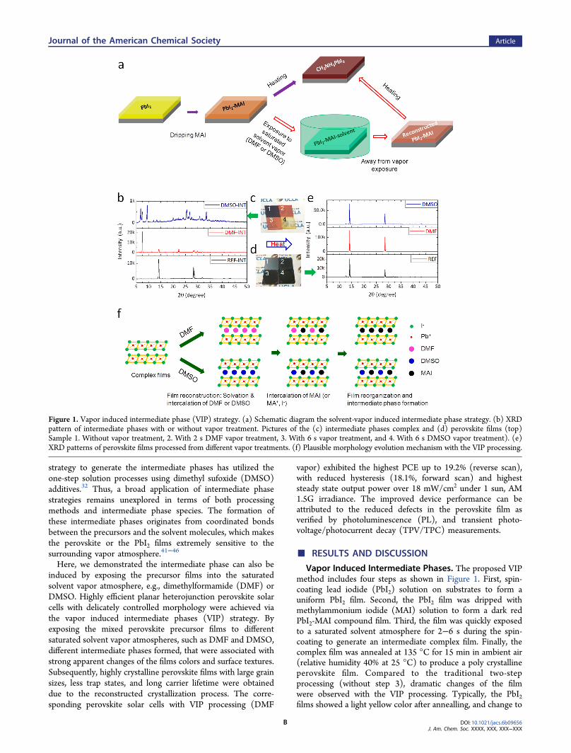
Vapor Induced Intermediate Phases. The proposed VIPmethod includes four steps as shown in Figure 1. First, spin-coating lead iodide (PbI2) solution on substrates to form auniform PbI2 film. Second, the PbI2 film was dripped withmethylammonium iodide (MAI) solution to form a dark redPbI2-MAI compound film. Third, the film was quickly exposedto a saturated solvent atmosphere for 2−6 s during the spin-coating to generate an intermediate complex film. Finally, thecomplex film was annealed at 135 °C for 15 min in ambient air(relative humidity 40% at 25 °C) to produce a poly crystallineperovskite film. Compared to the traditional two-stepprocessing (without step 3), dramatic changes of the filmwere observed with the VIP processing. Typically, the PbI2films showed a light yellow color after annealling, and change to
Figure 1. Vapor induced intermediate phase (VIP) strategy. (a) Schematic diagram the solvent-vapor induced intermediate phase strategy. (b) XRDpattern of intermediate phases with or without vapor treatment. Pictures of the (c) intermediate phases complex and (d) perovskite films (top)Sample 1. Without vapor treatment, 2. With 2 s DMF vapor treatment, 3. With 6 s vapor treatment, and 4. With 6 s DMSO vapor treatment). (e)XRD patterns of perovskite films processed from different vapor treatments. (f) Plausible morphology evolution mechanism with the VIP processing.
Journal of the American Chemical Society Article
DOI: 10.1021/jacs.6b09656J. Am. Chem. Soc. XXXX, XXX, XXX−XXX
B
dark red (Figure 1c) with the dripping of MAI due to theformation of the perovskite structure. With the vaportreatments, the dark red color of the precursor films initiallyfaded and became more transparent, followed by turning to awhite-to-red hazy color (with DMF vapor, top inset of Figure1) or white-to-yellow haze (Figure 1 c).Figure 1b depicts the XRD patterns of the PbI2-MAI
complex films. As shown, the films without vapor treatmentshowed peaks at 14.1° and 28.6°, corresponding to the ⟨110⟩and ⟨220⟩ faces of perovskite crystals as illustrated in previousworks.22 The appearance of perovskite peaks suggested that theprecursors were directly converted into the perovskitestructures upon MAI dripping in the traditional solution two-step method. However, a new peak at 28.3° appeared in theprecursor films, and disappeared after converting into perov-skite films with annealing on hot plate (Figure S1). Theappearance of the peak at 28.3° might result from theincomplete conversion of the precursors into the perovskitestructure after MAI dripping. However, with the VIP process,the XRD peaks corresponding to the perovskite structuredisappeared. Instead, three peaks at low diffraction angles of6.8°, 7.5° and 9.5° emerged with DMSO vapor treatment, andthese peaks were attributed to the formation of PbI2-MAI-DMSO complex as observed in previous work with one-stepsolution process.36,39 Interestingly, with the DMF vaportreatment, a new and distinctly strong peak at 7.5° appeared,corresponding to a lattice spacing of ∼1.17 nm. These resultsclearly show that the solvent vapor treatment is an effectivemethod to induce the formation of different intermediatephases. It is worth noting that the intermediate phases obtainedby VIP processing with DMF vapor is unprecedented inliterature. Thus, our work opens up a novel mechanism toconverting the precursor films into perovskite.To provide an insight into the intermediate phases structures,
we further analyzed the composition of the intermediate phasesvia Fourier transform infrared spectroscopy (FTIR), as shownin Figure S2. Compared to those without any vapor treatment,the precursor complex films with DMSO treatment showed anapparent absorption peak at 1017 cm−1, which can be attributedto the SO vibration. This observation is consistent with theprevious literature report, and confirms the existence of DMSOin the intermediate phases.36 However, the FTIR spectra ofPbI2-MAI precursor complex films with DMF treatment weresimilar to those without vapor exposure, and no peakscorresponding to the DMF molecules were observed inperovskite films with the DMF vapor exposure. This impliesthat the intermediate phases with DMF exposure are free ofDMF solvent molecules. Furthermore, we studied the XRDpatterns of pure PbI2 films with and without DMF or DMSOvapor treatment (Figure S3) and compared them with those ofthe PbI2-MAI intermediate phases. The XRD pattern of purePbI2 showed strong diffraction peak at 12.7°. Additionaldiffraction peaks appeared at 9.5° and 9.0° with DMF vaportreatment, and at 9.9° and 9.4° with the DMSO vaportreatment. It is clear that the peaks positions of pristine PbI2after DMSO or DMF vapor exposure were significant differentfrom that of intermediate phases of the PbI2-MAI complexes.This implied the involvement of both MAI and PbI2component in the intermediate phases. Therefore, it isconcluded that the intermediate phases are composed ofPbI2-MAI with DMF vapor treatment, and PbI2-MAI-DMSOwith the DMSO vapor treatment.
On the basis of the above analysis, plausible phase transitionmechanisms from the vapor treatments are drawn in Figure 1d.First, the DMF or DMSO solvent molecules may facilitate theinterdiffusion between the PbI2 and MAI layers due to thesolvation of the PbI2-MAI complex film by the saturated DMFor DMSO vapor surroundings. Second, the DMF or DMSOvapor treatment assists the intercalation of the MAI moleculeinto the PbI2 crystal lattice. It has been shown that the PbI2crystal exhibits lamellar structure with a plane of Pb2+ ionssandwiched between adjacent layers of hexagonally arrangediodide ions. The large interlayer space and weak interlayerinteraction allow the intercalation of different guest molecules,resulting in the expansion of the interlayer distance along the caxis.47 Due to the strong interaction between the PbI2 and theDMF or DMSO molecules, the interlayer distance of PbI2 isexpanded by DMF or DMSO vapor treatment, as proved by theappearance of low diffraction angle peaks of PbI2 films (FigureS3). Thereafter, the MAI molecules can be easily embeddedinto the lattice structure of PbI2, which accounts for the originof intermediate phase formation. Afterward, the DMF solventmolecule can escape from the intermediate phase due to thelow boiling point and weak interaction with Pb2+, resting theintercalated MAI component in the PbI2 crystal lattice. In thecase of DMSO exposure, the DMSO molecules remain in theintermediate phase due to their high boiling point and thestronger coordinated interaction with the Pb2+. Interdiffusionbetween the PbI2 and MAI is the most important step for thesolution-processed two-step method, and we can see that theformation of intermediate phase can significantly influence thecrystallization kinetics. As a result, changes in the morphologiesof the perovskite films are expected with the solvent vaportreatment on PbI2-MAI complex films, which were examined asfollow.
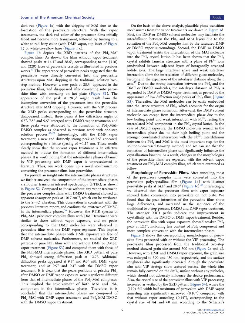
Morphology of Perovskite Films. After annealing, mostof the precursors complex films were converted into theperovskite polycrystalline film (Figure 1d) with distinctperovskite peaks at 14.1° and 28.6° (Figure 1c).28 Interestingly,we observed that the precursor films with vapor exposureshowed faster conversion into perovskite on hot plate. Wefound that the peak intensities of the perovskite films showlarge differences, and increased in the sequence of thetraditional two-step process, DMSO and DMF vapor treatment.The stronger XRD peaks indicate the improvement incrystallinity with the DMSO or DMF vapor treatment. Besides,the perovskite film with vapor exposure showed weaker PbI2peak at 12.7°, indicating less content of PbI2 component andmore complete conversion with the intermediate phases.Figure 2 shows the corresponding morphologies of perov-
skite films processed with or without the VIP processing. Theperovskite films processed from the traditional two-stepmethod showed grain size around 300 nm (Figure 2a and d).However, with DMF and DMSO vapor exposure, the grain sizewas enlarged to 500 and 450 nm, respectively, and the surfaceroughness also significantly increased. Altough the perovskitefilm with VIP strategy show textured surface, the whole filmremain fully covered on the SnO2 surface without any pinholes,which should not adversely influence the device performance.Also, the crystal size of the perovskite films with VIP processingincreased as verified by the XRD pattern (Figure S4), where the⟨110⟩ full-width-half-maximum of perovskite with DMF vaporannealing was significantly narrowed (0.10°) compared withthat without vapor annealing (0.14°), corresponding to thecrystal size of 84 and 60 nm according to the Scherrer’s
Journal of the American Chemical Society Article
DOI: 10.1021/jacs.6b09656J. Am. Chem. Soc. XXXX, XXX, XXX−XXX
C
equation (τ = Kλ/β cos θ, where K is geometry factor, λ is thewavelength of X-ray, β is the half-peak width, and θ is thediffraction angle). Although the perovskite grain size becamesignificantly larger, these large crystals were compactly arrangedon the surface of ITO/SnO2 substrates without any pin-holes,
as confirmed by the cross-sectional images (Figure S5). Theenlarged crystal size and more complete conversion from theprecursor to the perovskite films verifies the vapor inducedintermediate phases as an effective strategy to achieve highquality perovskite film.
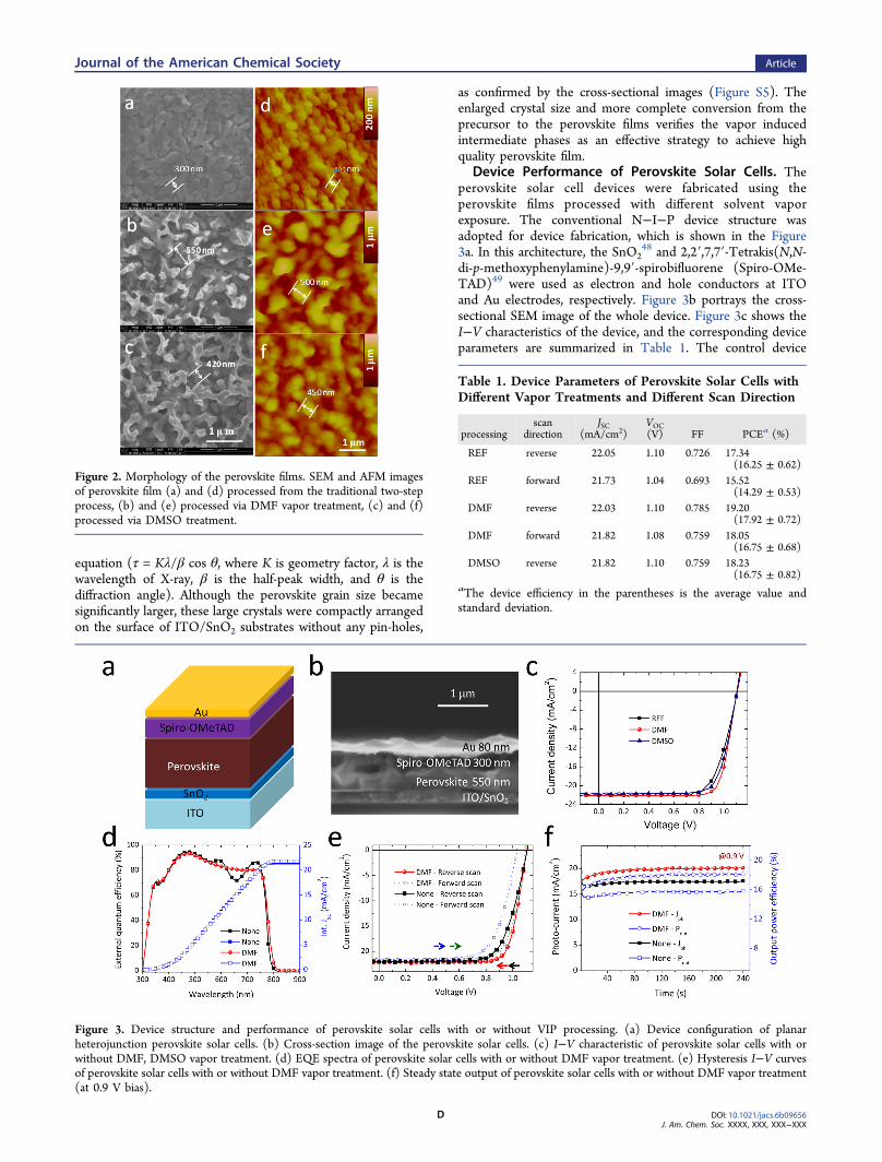
Device Performance of Perovskite Solar Cells. Theperovskite solar cell devices were fabricated using theperovskite films processed with different solvent vaporexposure. The conventional N−I−P device structure wasadopted for device fabrication, which is shown in the Figure3a. In this architecture, the SnO2
48 and 2,2′,7,7′-Tetrakis(N,N-di-p-methoxyphenylamine)-9,9′-spirobifluorene (Spiro-OMe-TAD)49 were used as electron and hole conductors at ITOand Au electrodes, respectively. Figure 3b portrays the cross-sectional SEM image of the whole device. Figure 3c shows theI−V characteristics of the device, and the corresponding deviceparameters are summarized in Table 1. The control device
Figure 2. Morphology of the perovskite films. SEM and AFM imagesof perovskite film (a) and (d) processed from the traditional two-stepprocess, (b) and (e) processed via DMF vapor treatment, (c) and (f)processed via DMSO treatment.
Figure 3. Device structure and performance of perovskite solar cells with or without VIP processing. (a) Device configuration of planarheterojunction perovskite solar cells. (b) Cross-section image of the perovskite solar cells. (c) I−V characteristic of perovskite solar cells with orwithout DMF, DMSO vapor treatment. (d) EQE spectra of perovskite solar cells with or without DMF vapor treatment. (e) Hysteresis I−V curvesof perovskite solar cells with or without DMF vapor treatment. (f) Steady state output of perovskite solar cells with or without DMF vapor treatment(at 0.9 V bias).
Table 1. Device Parameters of Perovskite Solar Cells withDifferent Vapor Treatments and Different Scan Direction
processingscan
directionJSC
(mA/cm2)VOC(V) FF PCEa (%)
REF reverse 22.05 1.10 0.726 17.34(16.25 ± 0.62)
REF forward 21.73 1.04 0.693 15.52(14.29 ± 0.53)
DMF reverse 22.03 1.10 0.785 19.20(17.92 ± 0.72)
DMF forward 21.82 1.08 0.759 18.05(16.75 ± 0.68)
DMSO reverse 21.82 1.10 0.759 18.23(16.75 ± 0.82)
aThe device efficiency in the parentheses is the average value andstandard deviation.
Journal of the American Chemical Society Article
DOI: 10.1021/jacs.6b09656J. Am. Chem. Soc. XXXX, XXX, XXX−XXX
D

processed with the traditional two-step method exhibited a bestPCE of 17.34%, with VOC of 1.10 V, JSC of 22.05 mA/cm2, andFF of 0.726. After the DMSO solvent vapor exposure, thedevice performance appreciably improved to 18.23%, with VOCof 1.10 V, JSC of 21.82 mA/cm2, and FF of 0.759. With theDMF vapor treatment, the device performance was furtherenhanced to 19.20%, with VOC of 1.10 V, JSC of 22.03 mA/cm2,and FF of 0.785, which stand among the highest in perovskitesolar cells with planar heterojunction configuration. Variation inthe device performances of perovskite solar cells from differentbatches were observed, and the statistic histogram for thedevice performance variation is shown in Figure S6. We alsostudied the effect of vapor treatment time on the deviceperformance. As shown in Figure S7, the device performance ofperovskite solar cells with a vapor treatment time from 2 to 6 sshowed improvement, but dropped when exposure time islonger than 6 s due to the poor morphology. Figure 3d showedthe external quantum efficiency of the perovskite solar cell withor without DMF vapor annealing. The highest EQE peak canreach up to 94%, implying the efficacy of the deviceconfiguration for light trapping and charge generation. Theintegrated JSC from the EQE spectra of the perovskite solar cellswithout vapor annealing was as high as 21.44 mA/cm2, andfurther improved to 21.66 mA/cm2 with DMF vapor treatment.These values were consistent (less than 3% deviation) with themeasured JSC from the scanned I−V curves, thus confirming thevalidity of the device performance. Although the integrated JSCsof perovskite solar cells with or without vapor annealing weresimilar, the EQE spectra showed large differences. The EQEprofiles of perovskite solar cells from DMF vapor treatmentwere more similar to the absorption spectra of the perovskitefilms (Figure S8), and the interference-induced peaks andvalleys (EQE spectra of perovskite solar cells without vaporexposure, and Figure S9 for the simulated optical fielddistribution in the control device) disappeared. We simulatedthe EQE spectra of the perovskite solar cells to confirmed the
origin of “V” shape, and ascribe it the a comprehensive effect ofeach layer via optical interference. As can be seen, the positionof the “V” shape can be altered by changing the perovskite andspiro-OMeTAD layer thickness. Thereafter, the diminish of “V”shape EQE can be attributed to the increased surface roughnesswith DMF vapor treatment. The irregular light scattering of therough perovskite layer can weaken the interference effect fromthe flat interface. This results indicates great potential of theVIP processing technique for optical manipulation in perovskitesolar cells.Hysteresis is typically observed in perovskite solar cells due
to the defect states or surface charging induced by ionmigration,50 which can be related to a variety of factors, such asinterfacial contact and morphology. Figure 3e shows thehysteresis effect of the I−V curves for devices with thetraditional two-step method and the DMF VIP processing. Forthe control device, a large discrepancy between the reverse andforward scan is observed, and the forward scan displays a lowerFF (0.693), VOC (1.04 V), and the overall PCE (15.52%),which represents over 10% reduction than that of the reversescan (17.34%). For the devices with DMF vapor exposure, thedevice parameters for the forward scanned show a FF of 0.759,VOC of 1.08 V, and overall PCE of 18.05%, which is within 6%deviation from that with reverse scan (19.20%). Thus,hysteresis can be appreciably suppressed by treating the filmwith DMF vapor. We attributed the alleviated hysteresis issueto the improved perovskite film quality, as described previously.The appearance of I−V hysteresis makes it difficult to
judiciously evaluate true device performance from the I−Vcurve scan. Thus, we further measured the steady state outputat the maximum power point to justify device performanceimprovement from VIP processing. As shown in Figure 3f, theperovskite solar cells without solvent vapor treatment exhibits amaximum photocurrent of 17.5 mA/cm2 at a bias of 0.90 Vunder 1 sun AM 1.5 G solar spectra, corresponding to themaximum power output of 15.75 mW/cm2. With DMF vapor
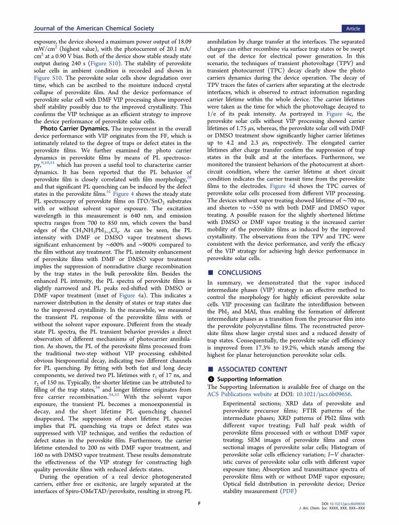
Figure 4. Carrier dynamics in perovskite films and perovskite solar cells. (a) Steady state PL spectra and (b) transient PL of perovskite filmprocessed from different solvent vapors (None, DMF, and DMSO). (c) Transient photovoltage and (d) transient photocurrent of perovskite solarcells processed with different solvent vapor treatments (None, DMF, and DMSO).
Journal of the American Chemical Society Article
DOI: 10.1021/jacs.6b09656J. Am. Chem. Soc. XXXX, XXX, XXX−XXX
E
exposure, the device showed a maximum power output of 18.09mW/cm2 (highest value), with the photocurrent of 20.1 mA/cm2 at a 0.90 V bias. Both of the device show stable steady stateoutput during 240 s (Figure S10). The stability of perovskitesolar cells in ambient condition is recorded and shown inFigure S10. The perovskite solar cells show degradation overtime, which can be ascribed to the moisture induced crystalcollapse of perovskite film. And the device performance ofperovskite solar cell with DMF VIP processing show imporvedshelf stability possibly due to the improved crystallinity. Thisconfirms the VIP technique as an efficient strategy to improvethe device performance of perovskite solar cells.Photo Carrier Dynamics. The improvement in the overall
device performance with VIP originates from the FF, which isintimately related to the degree of traps or defect states in theperovskite films. We further examined the photo carrierdynamics in perovskite films by means of PL spectrosco-py,9,10,51 which has proven a useful tool to characterize carrierdynamics. It has been reported that the PL behavior ofperovskite film is closely correlated with film morphology,20
and that significant PL quenching can be induced by the defectstates in the perovskite films.51 Figure 4 shows the steady statePL spectroscopy of perovskite films on ITO/SnO2 substrateswith or without solvent vapor exposure. The excitationwavelength in this measurement is 640 nm, and emissionspectra ranges from 700 to 850 nm, which covers the bandedges of the CH3NH3PbI3−xClx. As can be seen, the PLintensity with DMF or DMSO vapor treatment showssignificant enhancement by ∼600% and ∼900% compared tothe film without any treatment. The PL intensity enhancementof perovskite films with DMF or DMSO vapor treatmentimplies the suppression of nonradiative charge recombinationby the trap states in the bulk perovskite film. Besides theenhanced PL intensity, the PL spectra of perovskite films isslightly narrowed and PL peaks red-shifted with DMSO orDMF vapor treatment (inset of Figure 4a). This indicates anarrower distribution in the density of states or trap states dueto the improved crystallinity. In the meanwhile, we measuredthe transient PL response of the perovskite films with orwithout the solvent vapor exposure. Different from the steadystate PL spectra, the PL transient behavior provides a directobservation of different mechanisms of photocarrier annihila-tion. As shown, the PL of the perovksite films processed fromthe traditional two-step without VIP processing exhibitedobvious biexponential decay, indicating two different channelsfor PL quenching. By fitting with both fast and long decaycomponents, we derived two PL lifetimes with τ1 of 17 ns, andτ2 of 150 ns. Typically, the shorter lifetime can be attributed tofilling of the trap states,34 and longer lifetime originates fromfree carrier recombination.34,52 With the solvent vaporexposure, the transient PL becomes a monoexponential indecay, and the short lifetime PL quenching channeldisappeared. The suppression of short lifetime PL speciesimplies that PL quenching via traps or defect states wassuppressed with VIP technique, and verifies the reduction ofdefect states in the perovskite film. Furthermore, the carrierlifetime extended to 200 ns with DMF vapor treatment, and160 ns with DMSO vapor treatment. These results demonstratethe effectiveness of the VIP strategy for constructing highquality perovskite films with reduced defects states.During the operation of a real device photogenerated
carriers, either free or excitonic, are largely separated at theinterfaces of Spiro-OMeTAD/perovksite, resulting in strong PL
annihilation by charge transfer at the interfaces. The separatedcharges can either recombine via surface trap states or be sweptout of the device for electrical power generation. In thisscenario, the techniques of transient photovoltage (TPV) andtransient photocurrent (TPC) decay clearly show the photocarriers dynamics during the device operation. The decay ofTPV traces the fates of carriers after separating at the electrodeinterfaces, which is observed to extract information regardingcarrier lifetime within the whole device. The carrier lifetimeswere taken as the time for which the photovoltage decayed to1/e of its peak intensity. As portrayed in Figure 4c, theperovskite solar cells without VIP processing showed carrierlifetimes of 1.75 μs, whereas, the perovskite solar cell with DMFor DMSO treatment show significantly higher carrier lifetimesup to 4.2 and 2.3 μs, respectively. The elongated carrierlifetimes after charge transfer confirm the suppression of trapstates in the bulk and at the interfaces. Furthermore, wemonitored the transient behaviors of the photocurrent at short-circuit condition, where the carrier lifetime at short circuitcondition indicates the carrier transit time from the perovskitefilms to the electrodes. Figure 4d shows the TPC curves ofperovskite solar cells processed from different VIP processing.The devices without vapor treating showed lifetime of ∼700 ns,and shorten to ∼550 ns with both DMF and DMSO vaportreating. A possible reason for the slightly shortened lifetimewith DMSO or DMF vapor treating is the increased carriermobility of the perovskite films as induced by the improvedcrystallinity. The observations from the TPV and TPC wereconsistent with the device performance, and verify the efficacyof the VIP strategy for achieving high device performance inperovskite solar cells.
■ CONCLUSIONSIn summary, we demonstrated that the vapor inducedintermediate phases (VIP) strategy is an effective method tocontrol the morphology for highly efficient perovskite solarcells. VIP processing can facilitate the interdiffusion betweenthe PbI2 and MAI, thus enabling the formation of differentintermediate phases as a transition from the precursor film intothe perovskite polycrystalline films. The reconstructed perov-skite films show larger crystal sizes and a reduced density oftrap states. Consequentially, the perovskite solar cell efficiencyis improved from 17.3% to 19.2%, which stands among thehighest for planar heterojunction perovskite solar cells.
■ ASSOCIATED CONTENT*S Supporting InformationThe Supporting Information is available free of charge on theACS Publications website at DOI: 10.1021/jacs.6b09656.
Experimental sections; XRD data of perovskite andperovskite precursor films; FTIR patterns of theintermediate phases; XRD patterns of PbI2 films withdifferent vapor treating; Full half peak width ofperovskite films processed with or without DMF vaportreating; SEM images of perovskite films and crosssectional images of perovskite solar cells; Histogram ofperovskite solar cells efficiency variation; I−V character-istic curves of perovskite solar cells with different vaporexposure time; Absorption and transmittance spectra ofperovskite films with or without DMF vapor exposure;Optical field distribution in perovskite device; Devicestability measurement (PDF)
Journal of the American Chemical Society Article
DOI: 10.1021/jacs.6b09656J. Am. Chem. Soc. XXXX, XXX, XXX−XXX
F
■ AUTHOR INFORMATION
Corresponding Author*[email protected]
ORCIDYang Yang: 0000-0001-8833-7641NotesThe authors declare no competing financial interest.
■ ACKNOWLEDGMENTS
This work was financially supported by a grant from the Officeof Naval Research (Grant No. N000141110250), UCLAInternal Funds, the UC-Solar Program (Fund Number MRPI328368), and the Enli Tech (in Taiwan) for donating the EQEmeasurement system to UCLA. We also like to acknowledgeMr. Ryan Henry and Prof. Bruce Dunn for helping with theFTIR measurement. We thank Dr. Yajie Jiang, and Prof. AnitoHo-Baillie for providing the n and k values of the layers inperovskite devices.
■ REFERENCES(1) Park, N.-G. Mater. Today 2015, 18, 65.(2) Hodes, G. Science 2013, 342, 317.(3) Stranks, S. D.; Snaith, H. J. Nat. Nanotechnol. 2015, 10, 391.(4) Jeon, N. J.; Noh, J. H.; Yang, W. S.; Kim, Y. C.; Ryu, S.; Seo, J.;Seok, S. I. Nature 2015, 517, 476.(5) Jung, H. S.; Park, N.-G. Small 2015, 11, 10.(6) Chen, Q.; De Marco, N.; Yang, Y.; Song, T.-B.; Chen, C.-C.;Zhao, H.; Hong, Z.; Zhou, H.; Yang, Y. Nano Today 2015, 10, 355.(7) Juarez-Perez, E. J.; Sanchez, R. S.; Badia, L.; Garcia-Belmonte, G.;Kang, Y. S.; Mora-Sero, I.; Bisquert, J. J. Phys. Chem. Lett. 2014, 5,2390.(8) Brenner, T. M.; Egger, D. A.; Kronik, L.; Hodes, G.; Cahen, D.Nat. Rev. Mater. 2016, 1, 15007.(9) Stranks, S. D.; Eperon, G. E.; Grancini, G.; Menelaou, C.;Alcocer, M. J. P.; Leijtens, T.; Herz, L. M.; Petrozza, A.; Snaith, H. J.Science 2013, 342, 341.(10) Szuromi, P. Science 2015, 347, 960.(11) Oga, H.; Saeki, A.; Ogomi, Y.; Hayase, S.; Seki, S. J. Am. Chem.Soc. 2014, 136, 13818.(12) Baumann, A.; Vath, S.; Rieder, P.; Heiber, M. C.; Tvingstedt, K.;Dyakonov, V. J. Phys. Chem. Lett. 2015, 6, 2350.(13) Li, Y.; Meng, L.; Yang, Y.; Xu, G.; Hong, Z.; Chen, Q.; You, J.;Li, G.; Yang, Y.; Li, Y. Nat. Commun. 2016, 7, 10214.(14) Susrutha, B.; Giribabu, L.; Singh, S. P. Chem. Commun. 2015, 51,14696.(15) Gu, Z.; Zuo, L.; Larsen-Olsen, T. T.; Ye, T.; Wu, G.; Krebs, F.C.; Chen, H. J. Mater. Chem. A 2015, 3, 24254.(16) Schmidt, T. M.; Larsen-Olsen, T. T.; Carle, J. E.; Angmo, D.;Krebs, F. C. Adv. Energy Mater. 2015, 5, 1500569.(17) Hwang, K.; Jung, Y.-S.; Heo, Y.-J.; Scholes, F. H.; Watkins, S. E.;Subbiah, J.; Jones, D. J.; Kim, D.-Y.; Vak, D. Adv. Mater. 2015, 27,1241.(18) McGehee, M. D. Nat. Mater. 2014, 13, 845.(19) Salim, T.; Sun, S.; Abe, Y.; Krishna, A.; Grimsdale, A. C.; Lam,Y. M. J. Mater. Chem. A 2015, 3, 8943.(20) de Quilettes, D. W.; Vorpahl, S. M.; Stranks, S. D.; Nagaoka, H.;Eperon, G. E.; Ziffer, M. E.; Snaith, H. J.; Ginger, D. S. Science 2015,348, 683.(21) Eperon, G. E.; Burlakov, V. M.; Docampo, P.; Goriely, A.;Snaith, H. J. Adv. Funct. Mater. 2014, 24, 151.(22) Park, N.-G. CrystEngComm 2016, 18, 5977.(23) Bi, C.; Shao, Y.; Yuan, Y.; Xiao, Z.; Wang, C.; Gao, Y.; Huang, J.J. Mater. Chem. A 2014, 2, 18508.(24) Aharon, S.; Layani, M.; Cohen, B.-E.; Shukrun, E.; Magdassi, S.;Etgar, L. Adv. Mater. Interfaces 2015, 2, 1500118.
(25) Yang, W. S.; Noh, J. H.; Jeon, N. J.; Kim, Y. C.; Ryu, S.; Seo, J.;Seok, S. I. Science 2015, 348, 1234.(26) Burschka, J.; Pellet, N.; Moon, S.-J.; Humphry-Baker, R.; Gao,P.; Nazeeruddin, M. K.; Gratzel, M. Nature 2013, 499, 316.(27) Wang, Q.; Shao, Y.; Dong, Q.; Xiao, Z.; Yuan, Y.; Huang, J.Energy Environ. Sci. 2014, 7, 2359.(28) Liu, M.; Johnston, M. B.; Snaith, H. J. Nature 2013, 501, 395.(29) Chen, Q.; Zhou, H.; Hong, Z.; Luo, S.; Duan, H.-S.; Wang, H.-H.; Liu, Y.; Li, G.; Yang, Y. J. Am. Chem. Soc. 2014, 136, 622.(30) Bi, C.; Wang, Q.; Shao, Y.; Yuan, Y.; Xiao, Z.; Huang, J. Nat.Commun. 2015, 6, 8747.(31) Wang, Q.; Dong, Q.; Li, T.; Gruverman, A.; Huang, J. Adv.Mater. 2016, 28, 6734.(32) Yan, K.; Long, M.; Zhang, T.; Wei, Z.; Chen, H.; Yang, S.; Xu, J.J. Am. Chem. Soc. 2015, 137, 4460.(33) Liang, P.-W.; Liao, C.-Y.; Chueh, C.-C.; Zuo, F.; Williams, S. T.;Xin, X.-K.; Lin, J.; Jen, A. K. Y. Adv. Mater. 2014, 26, 3748.(34) Bi, D.; Tress, W.; Dar, M. I.; Gao, P.; Luo, J.; Renevier, C.;Schenk, K.; Abate, A.; Giordano, F.; Correa Baena, J.-P.; Decoppet, J.-D.; Zakeeruddin, S. M.; Nazeeruddin, M. K.; Gratzel, M.; Hagfeldt, A.Sci. Adv. 2016, 2, e1501170.(35) Zuo, L.; Gu, Z.; Ye, T.; Fu, W.; Wu, G.; Li, H.; Chen, H. J. Am.Chem. Soc. 2015, 137, 2674.(36) Jeon, N. J.; Noh, J. H.; Kim, Y. C.; Yang, W. S.; Ryu, S.; Seok, S.I. Nat. Mater. 2014, 13, 897.(37) Kim, J.; Hwang, T.; Lee, S.; Lee, B.; Kim, J.; Jang, G. S.; Nam, S.;Park, B. Sci. Rep. 2016, 6, 25648.(38) Rong, Y.; Venkatesan, S.; Guo, R.; Wang, Y.; Bao, J.; Li, W.; Fan,Z.; Yao, Y. Nanoscale 2016, 8, 12892−12899.(39) Rong, Y.; Tang, Z.; Zhao, Y.; Zhong, X.; Venkatesan, S.;Graham, H.; Patton, M.; Jing, Y.; Guloy, A. M.; Yao, Y. Nanoscale2015, 7, 10595.(40) Ahn, N.; Son, D.-Y.; Jang, I.-H.; Kang, S. M.; Choi, M.; Park, N.-G. J. Am. Chem. Soc. 2015, 137, 8696.(41) El-Henawey, M. I.; Gebhardt, R. S.; El-Tonsy, M. M.;Chaudhary, S. J. Mater. Chem. A 2016, 4, 1947.(42) Liu, J.; Gao, C.; He, X.; Ye, Q.; Ouyang, L.; Zhuang, D.; Liao,C.; Mei, J.; Lau, W. ACS Appl. Mater. Interfaces 2015, 7, 24008.(43) Li, Y.; Cooper, J. K.; Buonsanti, R.; Giannini, C.; Liu, Y.; Toma,F. M.; Sharp, I. D. J. Phys. Chem. Lett. 2015, 6, 493.(44) Lian, J.; Wang, Q.; Yuan, Y.; Shao, Y.; Huang, J. J. Mater. Chem.A 2015, 3, 9146.(45) Yu, H.; Liu, X.; Xia, Y.; Dong, Q.; Zhang, K.; Wang, Z.; Zhou,Y.; Song, B.; Li, Y. J. Mater. Chem. A 2016, 4, 321.(46) Xiao, Z.; Dong, Q.; Bi, C.; Shao, Y.; Yuan, Y.; Huang, J. Adv.Mater. 2014, 26, 6503.(47) Beckmann, P. A. Cryst. Res. Technol. 2010, 45, 455.(48) Ke, W.; Fang, G.; Liu, Q.; Xiong, L.; Qin, P.; Tao, H.; Wang, J.;Lei, H.; Li, B.; Wan, J.; Yang, G.; Yan, Y. J. Am. Chem. Soc. 2015, 137,6730.(49) Kim, H.-S.; Lee, C.-R.; Im, J.-H.; Lee, K.-B.; Moehl, T.;Marchioro, A.; Moon, S.-J.; Humphry-Baker, R.; Yum, J.-H.; Moser, J.E.; Gratzel, M.; Park, N.-G. Sci. Rep. 2012, 2, 591.(50) Chen, B.; Yang, M.; Priya, S.; Zhu, K. J. Phys. Chem. Lett. 2016,7, 905.(51) Noel, N. K.; Abate, A.; Stranks, S. D.; Parrott, E. S.; Burlakov, V.M.; Goriely, A.; Snaith, H. J. ACS Nano 2014, 8, 9815.(52) Marco, N. D.; Zhou, H.; Chen, Q.; Sun, P.; Liu, Z.; Meng, L.;Yao, E.-P.; Liu, Y.; Schiffer, A.; Yang, Y. Nano Lett. 2016, 16, 1009.
Journal of the American Chemical Society Article
DOI: 10.1021/jacs.6b09656J. Am. Chem. Soc. XXXX, XXX, XXX−XXX
G