motor monitoring preventive maintenance reference … · sensing to determine if preventative...
TRANSCRIPT

TIDA-01469 LaunchPad
CC1350
Flash memory
Coin Cell
Interrupt
TPS61291Boost Converter
REF5030VREF
ADS886616-bit ADC
OPA2325Op Amp
Piezo Accelerometer (66192CPZ1)
LMT01Temperature Sensor
VDD
VDD
VDD SPI
VBATT
VREF
TPS22860Load Switch
DVDD
40-p
in c
onne
ctor
Copyright © 2017, Texas Instruments Incorporated
1TIDUDC2–September 2017Submit Documentation Feedback
Copyright © 2017, Texas Instruments Incorporated
Motor Monitoring Using Wireless Vibration Sensor Reference DesignEnabling Preventive Maintenance
TI Designs: TIDA-01469Motor Monitoring Using Wireless Vibration SensorReference Design Enabling Preventive Maintenance
DescriptionThis reference design is a low-power wirelesssubsystem that monitors motors using vibrationsensing to determine if preventative maintenance isnecessary. An FFT of the vibration data can be sentout to another device using either Bluetooth® lowenergy or Sub-1 GHz wireless protocols. The low-power usage and wireless capabilities of thissubsystem enables it to run on a single coin cellbattery, which allows for the device to be small,inexpensive, and placed in difficult-to-reach locations.These features makes this design an ideal alternativeto both expensive maintenance that could have beenpreventatively avoided as well as larger, moreexpensive monitors that require a wired connection.
Resources
TIDA-01469 Design FolderCC1350 Product FolderADS8866 Product FolderOPA2325 Product FolderTPS61291 Product FolderREF5030 Product FolderTPS22860 Product FolderLMT01 Product FolderLAUNCHXL-CC1350 Tool Folder
ASK Our E2E Experts
Features• Ultra-Low-Power Design Resulting in 10-Year
Battery Life From Single CR2032 Coin Cell• Offers Mechanical Vibration (20 kSPS) and
Temperature Sensing• Local Computation of 2K FFT for Vibration Spectral
Analysis• Programmable Wake-Up Intervals for Motor
Diagnostics• Designed For SimpleLink™ Sub-1 GHz and
Bluetooth Low Energy Wireless ConnectivityLaunchPad™ (LAUNCHXL-CC1350)
Applications• Remote Motor Health Monitoring• Wireless Machine Monitoring• Structural Monitoring

System Description www.ti.com
2 TIDUDC2–September 2017Submit Documentation Feedback
Copyright © 2017, Texas Instruments Incorporated
Motor Monitoring Using Wireless Vibration Sensor Reference DesignEnabling Preventive Maintenance
An IMPORTANT NOTICE at the end of this TI reference design addresses authorized use, intellectual property matters and otherimportant disclaimers and information.
1 System DescriptionMany industrial settings include motors that require maintenance as they age and stop working correctly.This maintenance is expensive, and significant downtime can occur if the need for maintenance is notpredicted and accounted for. Wireless monitors that can run on a single coin cell battery can be placedalmost anywhere and do not need to be accessed often, which is ideal for industrial settings.
The Motor Monitoring Using Wireless Vibration Sensor Reference Design provides a wireless motormonitoring subsystem that can run on a single CR2032 coin cell battery with 10+ year battery life. Thisallows for a small motor monitor that can be placed in difficult-to-reach locations and does not need to bereached often to change the battery or access the data with a wired connection.
This reference design uses Texas Instruments’ CC1350 SimpleLink Ultra-Low Power Dual Band WirelessMicrocontroller to read the sensor data, process this data by computing a 2K FFT, and send the data outover an ultra-low-power 2.4-GHz Bluetooth low energy or Sub-1 GHz network. The firmware provided inthis design guide uses Texas Instruments’ Bluetooth low energy software stack to send the FFT data outin notifications in a connection with another device.
At a high level, this reference design consists of a CR2032 coin cell battery, an ultra-low-power wirelessMCU, a piezoelectric accelerometer to acquire the vibration data, an analog-to-digital converter (ADC) tosample this data, and a load switch and boost convertor to gate power to the system. The real-time clockon the CC1350 MCU is used to only wake the system at configurable time intervals. When the system ispowered up, the accelerometer acquires the vibration data, the ADC converts the data and sends it to theMCU over SPI, the MCU computes the FFT of the data, and the data is sent to another device overBluetooth low energy. The device that receives the data can then indicate that the motor monitor canpower back down until it is time to take vibration measurements again. A temperature sensor is alsoprovided to monitor the ambient temperature and further help to predict the need for motor maintenance.
This design guide addresses component selection, design theory, and the testing results of this referencedesign system. The scope of this design allows designers to develop motor monitoring applications thatuse TI’s components for the analog front end (AFE) and TI’s SimpleLink ultra-low-power wireless MCUplatform.
The following subsections describe the key blocks within the reference design system and whatcharacteristics are most critical to best implement the corresponding functions.
1.1 Key System Specifications
Table 1. Key System Specifications
PARAMETER SPECIFICATIONS DETAILSInput power source CR2032 Lithium-ion coin cell battery (3.0-V nominal voltage) Section 2.2.6Sensor type Accelerometer Section 2.2.2Average standby-state current 879.5 nA Section 3.2.2.1Estimated battery life > 10 years Section 3.2.2.2Fourier transform 2048 points at 20 kSPS Section 3.2.2.3Frequency monitoring range 50 Hz to 10 kHz Section 3.2.2.3Operating temperature –30°C to 85°C Section 2.3Wireless protocol Bluetooth low energy Section 2.4.3Radio transmission range 72 meters Section 3.2.2.5Default reporting interval 8 hours (Can be dynamically selected) Section 2.4.4Form factor (sensor board) 58.50-mm × 95.30-mm rectangular PCB Section 3.1.1

TIDA-01469 LaunchPad
CC1350
Flash memory
Coin Cell
Interrupt
TPS61291Boost Converter
REF5030VREF
ADS886616-bit ADC
OPA2325Op Amp
Piezo Accelerometer (66192CPZ1)
LMT01Temperature Sensor
VDD
VDD
VDD SPI
VBATT
VREF
TPS22860Load Switch
DVDD
40-p
in c
onne
ctor
Copyright © 2017, Texas Instruments Incorporated
www.ti.com System Overview
3TIDUDC2–September 2017Submit Documentation Feedback
Copyright © 2017, Texas Instruments Incorporated
Motor Monitoring Using Wireless Vibration Sensor Reference DesignEnabling Preventive Maintenance
2 System Overview
2.1 Block Diagram
Figure 1. Block Diagram
2.2 Design Considerations
2.2.1 Ultra-Low-Power Wireless MCUIn this reference design, the acquired vibration data and the FFT of the data need to be sent to anotherdevice so that it can be used to determine if maintenance is or will soon be necessary. To allow for asmall device with a long enough battery life to justify putting the monitor in difficult-to-reach locations,however, the radio and processor must also be low power. The CC1350 has two antennas to allow data tobe transmitted over either Bluetooth low energy or Sub-1 GHz networks, depending on what device willreceive the data and how it will be stored and accessed. TI’s SimpleLink ultra-low-power wireless MCUplatform, with a combined radio and MCU, enables an extremely long battery life for wireless motormonitors.
2.2.2 Piezoelectric AccelerometerPiezoelectric accelerometers can accurately measure vibrations, which allows for the health of the motorto be quantified. This reference design uses the 66192CPZ1 from IMI Sensors®. This device has a goodsensitivity for the design, and its 10-kHz frequency range allows for a stable input signal to the ADC afterfiltering. It also has a high linearity, which allows for more accurate data.

System Overview www.ti.com
4 TIDUDC2–September 2017Submit Documentation Feedback
Copyright © 2017, Texas Instruments Incorporated
Motor Monitoring Using Wireless Vibration Sensor Reference DesignEnabling Preventive Maintenance
2.2.3 Analog-to-Digital ConversionThis reference design uses an ADC with external voltage reference to digitize the output of the op-ampstage. The ADS8866 is a 16-bit SAR ADC that provides the necessary resolution and sampling for thewireless motor monitor design. The device communicates with the MCU over SPI, and the high resolutionallows for an accurate FFT to be calculated and observed. The digital power supply of the ADC isconnected directly to the output of the battery to match the digital input/output pin voltage levels of thewireless MCU.
An external voltage reference source is used for the ADC to provide an output voltage that is stableacross ambient temperature, loading, input supply, and time. The REF5030 device provides a low-noise,low-drift, very high-precision voltage reference. The standard grade device has an initial output voltageaccuracy of ±0.1% (max), a temperature drift of 8 ppm/°C (max), a long-term stability of 45 ppm/1000 hrafter 1000 hours (typ), and an output voltage noise of 3 µVPP/V (typ).
At a 100-kHz sampling rate, the ADC consumes 230 µA when operated at 3 V while the voltage referencehas a quiescent current of 800 µA. To meet the battery life target for this reference design, it is necessaryto completely power off the ADC and voltage reference when the system is in standby mode. The ADCand voltage reference are powered on when a vibration measurement is needed.
2.2.4 Low-Leakage Boost ConverterSome sensor end-nodes require a regulated voltage rail to operate at their highest levels of sensingperformance. To provide a well-regulated voltage rail over the entire lifetime of the battery, a boostconverter is necessary. However, to reduce the battery life loss due to converter inefficiency, an extremelyhigh-efficiency boost converter is required.
In this reference design, the TPS61291 device regulates the battery voltage to 3.3 V. With a batteryvoltage of 3.0 V, the TPS61291 maintains an efficiency level greater than 95% at the load currents typicalof a sensor end-node: 1 to 100 mA. Even at the depleted coin cell voltage of 2.0 V, the TPS61291 devicemaintains an efficiency level greater than 90% over the typical load current range of 1 to 100 mA.
The boost converter provides the operating voltage for the sensor subsystem of the design, whichincludes the operational amplifiers, ADC, and voltage reference.
2.2.5 Low-Leakage Load SwitchThis reference design uses a low-leakage load switch to shut off power to the sensor subsystem of thedesign leaving only the CC1350 wireless MCU and temperature sensor with power. The sensorsubsystem includes the boost converter, operational amplifiers, ADC, and voltage reference. The mostimportant characteristic of this switch is the off-state leakage, because that leakage affects the overallbattery life of the system significantly.
In this reference design, the TPS22860 device is the switch used to disconnect the sensor subsystemfrom the battery. The TPS22860 has a typical leakage current of 2 nA at the VIN pin and 10 nA at theVBIAS pin, which enables extremely long battery life in this system.
2.2.6 Coin Cell BatteryThe power source for this reference design is a CR2032 lithium-ion coin cell. The CR2032 coin cell batteryis the power source because of the ubiquity of that battery type.
The voltage characteristics of a lithium-ion CR2032 coin cell battery are also ideal. The output voltageremains relatively flat throughout the discharge life until the cell is nearly depleted. When the cell isdepleted, the output voltage drops off relatively quickly.
Immediately following the battery are two low RDS_ON P-channel MOSFETs and a bulk capacitor. The P-channel MOSFETs prevent damage to the hardware if the coin cell battery is inserted backwards whileminimizing the forward voltage drop in normal operation. The bulk capacitor is sized to prevent too muchvoltage drop, particularly during the transitions into the MCU on-state for radio transmissions.

www.ti.com System Overview
5TIDUDC2–September 2017Submit Documentation Feedback
Copyright © 2017, Texas Instruments Incorporated
Motor Monitoring Using Wireless Vibration Sensor Reference DesignEnabling Preventive Maintenance
2.3 Highlighted ProductsThis motor monitoring reference design features the following devices:• OPA2325 (Section 2.3.1): Dual, precision, low-voltage CMOS operational amplifier• ADS8866 (Section 2.3.2): 16-bit, 100-kSPS, single-ended input, SAR analog-to-digital converter• REF5030 (Section 2.3.3): Low-noise, low-drift, very high precision voltage reference• TPS61291 (Section 2.3.4): Low-IQ boost converter• TPS22860 (Section 2.3.5): Ultra-low leakage current, single-channel load switch• LMT01 (Section 2.3.6): High-accuracy, 2-pin temperature sensor• CC1350 (Section 2.3.7): Ultra-low-power wireless SimpleLink MCU capable of handling both Sub-1
GHz and 2.4-GHz RF frequencies
For more information on each of these devices, see their respective product folders at TI.com.
2.3.1 OPA2325The OPA2325 device is a dual, precision, low-voltage complementary metal oxide semiconductor (CMOS)operational amplifier optimized for very low noise and wide bandwidth when operating on a low quiescentcurrent of only 650 μA.
The OPA2325 features a linear input stage with zero-crossover distortion that delivers excellent common-mode rejection ratio (CMRR) of typically 114 dB over the entire input range. The input common-moderange extends 100 mV beyond the negative and positive supply rails. The output voltage typically swingswithin 10 mV of the rails.
The zero-crossover distortion combined with wide bandwidth (10 MHz), high slew rate (5 V/μs), and lownoise (9 nV/√Hz) make the OPA2325 a very good successive-approximation register (SAR) ADC inputdriver amplifier. The low offset, and 0.2-pA input bias current make this device ideal for a wide range ofprecision applications with high-impedance sensors. The unique feature of interfacing to high-impedancesensors on the input and being able to drive ADC inputs with very little distortion make the OPA2325suitable for various data acquisition and process control applications.
In addition, the OPA2325 has a wide supply voltage range from 2.2 to 5.5 V with excellent power-supplyrejection ratio (PSRR) over the entire supply range, making the device suitable for precision, low-powerapplications that run directly from batteries without regulation.
Key features of this device include:• Precision with zero-crossover distortion:
– Low offset voltage: 150 μV (max)– High CMRR: 114 dB– Rail-to-rail I/O
• Wide bandwidth: 10 MHz• Quiescent current: 650 μA/ch• Single-supply voltage range: 2.2 to 5.5 V• Low input bias current: 0.2 pA• Low noise: 9 nV/√Hz at 10 kHz• Slew rate: 5 V/μs• Unity-gain stable
2.3.2 ADS8866The ADS8866 is a 16-bit, 100-kSPS, single-ended input ADC. The device operates with a 2.5- to 5-Vexternal reference, offering a wide selection of signal ranges without additional input signal scaling. Thereference voltage setting is independent of, and can exceed, the analog supply voltage (AVDD).
The device offers an SPI-compatible serial interface that also supports daisy-chain operation for cascadingmultiple devices.

System Overview www.ti.com
6 TIDUDC2–September 2017Submit Documentation Feedback
Copyright © 2017, Texas Instruments Incorporated
Motor Monitoring Using Wireless Vibration Sensor Reference DesignEnabling Preventive Maintenance
The device supports unipolar single-ended analog inputs in the range of –0.1 V to VREF + 0.1 V.
Device operation is optimized for very low-power operation. Power consumption directly scales withspeed. This feature makes the ADS8866 excellent for lower-speed applications.
Key features of this device include:• Sample rate: 100 kHz• No latency output• Unipolar, single-ended input range: 0 to +VREF• SPI-compatible serial interface with daisy-chain option• Excellent AC and DC performance:
– SNR: 93 dB, THD: –108 dB– INL: ±1.0 LSB (typ), ±2.0 LSB (max)– DNL: ±1.0 LSB (max), 16-bit NMC
• Wide operating range:– AVDD: 2.7 to 3.6 V– DVDD: 1.65 to 3.6 V (independent of AVDD)– Operating temperature: –40°C to 85°C
• Low-power dissipation:– 0.7 mW at 100 kSPS– 70 μW at 10 kSPS
• Power-down current (AVDD): 50 nA• Full-scale step settling to 16 bits: 1200 ns• Packages: MSOP-10 and SON-10
2.3.3 REF5030The REF5030 is a low-noise, low-drift, very high-precision voltage references. These references arecapable of both sinking and sourcing current and have excellent line and load regulation.
Excellent temperature drift (3 ppm/°C) and high accuracy (0.05%) are achieved using proprietary designtechniques. Combined with very low noise, these features make the REF5030 device ideal for use in high-precision data acquisition systems.
Each reference voltage is available in both high grade (REF50xxIDGK and REF50xxID) and standardgrade (REF50xxAIDGK and REF50xxAID). The reference voltages are offered in 8-pin VSSOP and SOICpackages and are specified from –40°C to 125°C.
Key features of this device include:• Low temperature drift:
– High-grade: 3 ppm/°C (Max)– Standard-grade: 8 ppm/°C (Max)
• High accuracy:– High-grade: 0.05% (Max)– Standard-grade: 0.1% (Max)
• Low noise: 3 μVPP/V• Excellent long-term stability:
– 45 ppm/1000 hr (typ) after 1000 hours• High-output current: ±10 mA• Temperature range: –40°C to 125°C

www.ti.com System Overview
7TIDUDC2–September 2017Submit Documentation Feedback
Copyright © 2017, Texas Instruments Incorporated
Motor Monitoring Using Wireless Vibration Sensor Reference DesignEnabling Preventive Maintenance
2.3.4 TPS61291The TPS61291 is a boost converter with pin mode. In bypass operation, the device provides a direct pathfrom the input to the system and allows a low-power MCU such as the MSP430™ to operate directly froma single 3-V Li-MnO2 battery or dual alkaline battery cells. In bypass mode, the integrated feedbackdivider network for boost mode operation is disconnected from the output and the quiescent currentconsumption drops down to only 15 nA (typical).
In boost mode, the device provides a minimum output current of 200 mA at 3.3-V VOUT from 1.8-V VIN. Theboost mode is used for system components that require a regulated supply voltage and cannot directlyoperate from the input source. The boost converter is based on a current-mode controller usingsynchronous rectification to obtain maximum efficiency and consumes typically 5.7 µA from the output.During startup of the boost converter, the VSEL pin is read out and the integrated feedback network setsthe output voltage to 2.5 V, 3 V, or 3.3 V.
Bypass mode or boost mode operation is controlled by the system through the EN/BYP pin.
The device integrates an enhanced bypass mode control to prevent charge, stored in the output capacitorduring boost mode operation, from flowing back to the input and charging the battery.
The device is packaged in a small 6-pin SON package (DRV) measuring 2.0 mm × 2.0 mm x 0.75 mm.
Key features of this device include:• Input voltage range: 0.9 to 5 V• Startup voltage: 1.5 V at 20-mA load• Pin selectable output voltages: 3.3 V, 3 V, 2.5 V• 15-nA typical quiescent current in bypass mode• 5.7-μA typical quiescent current in boost mode• Bypass switch from VIN to VOUT
• IOUT > 200 mA at 3.3-V VOUT, VIN = 1.8 V• Internal feedback divider disconnect (bypass mode)• Controlled bypass transition prevents reverse current into battery• Power-save mode at light loads• Overtemperature protection• Redundant overvoltage protection• Small 2-mm×2-mm SON 6-pin package
2.3.5 TPS22860The TPS22860 is a small, ultra-low leakage current, single-channel load switch. The device requires aVBIAS voltage and can operate over an input voltage range of 0 V to VBIAS. The device can support amaximum continuous current of 200 mA. The switch is controlled by an on/off input (ON), which is capableof interfacing directly with low-voltage control signals. The TPS22860 is available in two small, space-saving 6-pin SOT-23 and SC70 packages. The device is characterized for operation over the free-airtemperature range of –40°C to 85°C.• Integrated single-channel load switch• Bias voltage range (V single channel load switch. The device requires a BIAS): 1.65 to 5.5 V• Input voltage range: 0 V to VBIAS
• ON-resistance (RON)– RON = 0.73 Ω at VIN = 5 V (VBIAS = 5 V)– RON = 0.68 Ω at VIN = 3.3 V (VBIAS = 5 V)– RON = 0.63 Ω at VIN = 1.8 V (VBIAS = 5 V)
• 200-mA maximum continuous switch current• Ultra-low leakage current
– VIN leakage current = 2 nA

System Overview www.ti.com
8 TIDUDC2–September 2017Submit Documentation Feedback
Copyright © 2017, Texas Instruments Incorporated
Motor Monitoring Using Wireless Vibration Sensor Reference DesignEnabling Preventive Maintenance
– VBIAS leakage current at 5.5 V = 10 nA• 6-pin SOT-23 or SC70 package• ESD performance tested per JESD 22
– 2-kV HBM and 1-kV CDM
2.3.6 LMT01The LMT01 device is a high-accuracy, 2-pin temperature sensor with an easy-to-use pulse count currentloop interface, which makes it suitable for onboard and off-board applications in automotive, industrial, andconsumer markets. The LMT01 digital pulse count output and high accuracy over a wide temperaturerange allow pairing with any MCU without concern for integrated ADC quality or availability, whileminimizing software overhead. TI’s LMT01 device achieves a maximum ±0.5°C accuracy with very fineresolution (0.0625°C) over a temperature range of –20°C to 90°C without system calibration or hardwareand software compensation.
The LMT01’s pulse count interface is designed to directly interface with a GPIO or comparator input,thereby simplifying hardware implementation. Similarly, the LMT01's integrated EMI suppression andsimple 2-pin architecture makes it suitable for onboard and off-board temperature sensing in a noisyenvironment. The LMT01 device can be easily converted into a two-wire temperature probe with a wirelength up to two meters. See LMT01-Q1 for the automotive qualified version.
Key features of this device include:• High accuracy over –50°C to 150°C wide temperature range:
– –20°C to 90°C: ±0.5°C (maximum)– 90°C to 150°C: ±0.625°C (maximum)– –50°C to –20°C: ±0.7°C (maximum)
• Precision digital temperature measurement simplified in a 2-pin package• Pulse count current loop easily read by processor
– Number of output pulses is proportional to temperature with 0.0625°C resolution• Communication frequency: 88 kHz• Conversion current: 34 μA• Continuous conversion plus data-transmission period: 100 ms• Floating 2- to 5.5-V (VP–VN) supply operation with integrated EMI immunity• Multiple 2-pin package offerings: TO-92/LPG (3.1 mm × 4 mm × 1.5 mm)
– ½ the size of traditional TO-92 and WSON with wettable flanks
2.3.7 CC1350The CC1350 is a member of the CC26xx and CC13xx family of cost-effective, ultra-low-power, 2.4-GHzand Sub-1 GHz RF devices from Texas Instruments. Very low active RF and MCU current consumption, inaddition to flexible low-power modes, provide excellent battery lifetime and allow long-range operation onsmall coin cell batteries and in energy-harvesting applications.
The CC1350 is the first device in the CC13xx and CC26xx family of cost-effective, ultra-low-powerwireless MCUs capable of handling both Sub-1 GHz and 2.4-GHz RF frequencies. The CC1350 devicecombines a flexible, very low-power RF transceiver with a powerful 48-MHz ARM® Cortex® M3 MCU in aplatform supporting multiple physical layers and RF standards. A dedicated radio controller (Cortex-M0)handles low-level RF protocol commands that are stored in ROM or RAM, thus ensuring ultra-low powerand flexibility to handle both Sub-1 GHz protocols and 2.4-GHz protocols (for example, Bluetooth lowenergy). This enables the combination of a Sub-1 GHz communication solution that offers the bestpossible RF range together with a Bluetooth low energy smartphone connection that enables great userexperience through a phone application. The Sub-1 GHz only device in this family is the CC1310.
The CC1350 device is a highly integrated, true single-chip solution incorporating a complete RF systemand an on-chip DC-DC converter.

www.ti.com System Overview
9TIDUDC2–September 2017Submit Documentation Feedback
Copyright © 2017, Texas Instruments Incorporated
Motor Monitoring Using Wireless Vibration Sensor Reference DesignEnabling Preventive Maintenance
Sensors can be handled in a very low-power manner by a dedicated autonomous ultra-low-power MCUthat can be configured to handle analog and digital sensors; thus the main MCU (Cortex-M3) canmaximize sleep time.
The CC1350 power and clock management and radio systems require specific configuration and handlingby software to operate correctly, which has been implemented in the TI-RTOS. TI recommends using thissoftware framework for all application development on the device. The complete TI-RTOS and devicedrivers are offered in source code free of charge.
Key features of this device include:• Microcontroller:
– Powerful ARM Cortex-M3 processor– EEMBC CoreMark® Score: 142– EEMBC ULPBench™ Score: 158– Clock speed up to 48 MHz– 128kB of in-system programmable flash– 8kB of SRAM for cache (or as general-purpose RAM)– 20kB of ultra-low-leakage SRAM– 2-pin cJTAG and JTAG debugging– Supports over-the-air (OTA) update
• Ultra-low-power sensor controller– Can run autonomously from the rest of the system– 16-bit architecture– 2kB of ultra-low-leakage SRAM for code and data
• Efficient code-size architecture, placing parts of TI-RTOS, drivers, Bluetooth low energy controller, andbootloader in ROM
• RoHS-compliant package– 7-mm×7-mm RGZ VQFN48 (30 GPIOs)– 5-mm×5-mm RHB VQFN32 (15 GPIOs)– 4-mm×4-mm RSM VQFN32 (10 GPIOs)
• Peripherals– All digital peripheral pins can be routed to any GPIO– Four general-purpose timer modules (eight 16-bit or four 32-bit timers, PWM each)– 12-bit ADC, 200 kSPS, 8-channel analog MUX– Continuous time comparator– Ultra-low-power clocked comparator– Programmable current source– UART– 2× SSI (SPI, MICROWIRE, TI)– I2C, I2S– Real-time clock (RTC)– AES-128 security module– True random number generator (TRNG)– Support for eight capacitive sensing buttons– Integrated temperature sensor
• External system– On-chip internal DC-DC converter– Seamless integration with the SimpleLink CC1190 and CC2592 range extenders
• Low power
System Overview www.ti.com
10 TIDUDC2–September 2017Submit Documentation Feedback
Copyright © 2017, Texas Instruments Incorporated
Motor Monitoring Using Wireless Vibration Sensor Reference DesignEnabling Preventive Maintenance
– Wide supply voltage range: 1.8 to 3.8 V– RX: 5.4 mA (Sub-1 GHz), 6.4 mA (Bluetooth low energy, 2.4 GHz)– TX at 10 dBm: 13.4 mA (Sub-1 GHz)– TX at 9 dBm: 22.3 mA (Bluetooth low energy, 2.4 GHz)– TX at 0 dBm: 10.5 mA (Bluetooth low energy, 2.4 GHz)– Active-mode MCU: 48 MHz running Coremark: 2.5 mA (51 μA/MHz)– Active-mode MCU: 48.5 CoreMark/mA– Active-mode sensor controller at 24 MHz: 0.4 mA + 8.2 μA/MHz– Sensor controller, one wakeup every second performing one 12-bit ADC sampling: 0.95 μA– Standby: 0.7 μA (RTC running and RAM and CPU retention)– Shutdown: 185 nA (wakeup on external events)
• RF section– 2.4-GHz RF transceiver compatible with Bluetooth low energy 4.2 specification– Excellent receiver sensitivity: –124 dBm using long-range mode, –110 dBm at 50 kbps (Sub-1
GHz), –87 dBm at Bluetooth low energy– Excellent selectivity (±100 kHz): 56 dB– Excellent blocking performance (±10 MHz): 90 dB– Programmable output power up to 15 dBm (Sub-1 GHz) and 9 dBm at 2.4 GHz (Bluetooth low
energy)– Single-ended or differential RF interface– Suitable for systems targeting compliance with worldwide radio frequency regulations
• ETSI EN 300 220, EN 303 204 (Europe)• EN 300 440 Class 2 (Europe)• EN 300 328 (Europe)• FCC CFR47 Part 15 (US)• ARIB STD-T66 (Japan)• ARIB STD-T108 (Japan)
– Wireless M-Bus and selected IEEE® 802.15.4g PHY• Tools and development environment
– Full-feature and low-cost development kits– Multiple reference designs for different RF configurations– Packet sniffer PC software– Sensor Controller Studio– SmartRF™ Studio– SmartRF Flash Programmer 2– IAR Embedded Workbench® for ARM– Code Composer Studio™

B 2
1
2 R Cp
1 2AMP
1 2 IN 1
C RS 1
C C C R
æ ö= ´ +ç ÷
+ + è ø
1S
1 2 IN
CS
C C C=
+ +
C1
1 V/g C2
Piezo Vibration Sensor
+1.4 V
RB
+
±
OPA325
RL
CL
VOUT
+1.4 VR1
+3.0 V
CF
R2
Copyright © 2017, Texas Instruments Incorporated
www.ti.com System Overview
11TIDUDC2–September 2017Submit Documentation Feedback
Copyright © 2017, Texas Instruments Incorporated
Motor Monitoring Using Wireless Vibration Sensor Reference DesignEnabling Preventive Maintenance
2.4 System Design Theory
2.4.1 Analog Front EndTo monitor machine vibrations, this design uses a piezo vibration sensor. Because piezo sensors havehigh-impedance output nodes, the AFE circuitry was carefully designed to reduce the noise and increasethe sensitivity of the system. For the AFE circuitry with piezo sensor, see Figure 2. The amplifier and thesensor affect the noise and sensitivity values of the AFE. Because of this effect, proper modeling of thesensor helps to analyze the noise and sensitivity of the AFE. Piezoelectric vibration sensors are typicallyused in much lower-frequency domains than resonant frequency. These sensors can be electricallymodeled as a voltage source that converts force to voltage through two capacitors, C1 and C2. For thesecapacitors, see Figure 2. This model disregards the noise of the sensor because it is typically much lessthan the noise of the interface circuitry.
Figure 2. AFE Schematic With Piezo Vibration Sensor
The sensitivity at the sensor output, SS, is defined by Equation 1.
(1)
where:• CIN is the input common-mode capacitor of the amplifier
Because a large CIN reduces the SS, it is desirable to make CIN small in comparison to C2. However,because the piezo sensors are high-impedance output sensors, CMOS or JFET input amplifiers aredesirable but typically have large CIN for low flicker noise. The OPA325 and the PCB Piezotronics sensorresult in good performance when these constraints are taken into consideration because the CIN of theOPA325 is 4 pF, which is very small compared to the 350 pF of the PCB Piezotronics sensor capacitance,and the OPA325 has low-input referred voltage noise, Vn, and low-input referred current noise, In.
The sensitivity of the amplifier output, SAMP, is defined by Equation 2.
(2)
The resistor, RB, is necessary for the DC bias at the amplifier input, and it sets a high-pass filter with thesensor output capacitance.
The cut-off frequency of the high-pass filter ≈ .
The capacitors, CF and CL, set low-pass filters with R2 and RL, respectively.

2 F
1
2 R Cp
L L
1
2 R Cp
System Overview www.ti.com
12 TIDUDC2–September 2017Submit Documentation Feedback
Copyright © 2017, Texas Instruments Incorporated
Motor Monitoring Using Wireless Vibration Sensor Reference DesignEnabling Preventive Maintenance
The cutoff frequency of low-pass filter 1 is shown in Equation 3.
(3)
The cutoff frequency of low-pass filter 2 is shown in Equation 4.
(4)
A TINA-TI™ simulation is run to determine the upper and lower cutoff frequencies. The upper cutofffrequency is shown to be 11.3 kHz, as shown in Figure 3.
Figure 3. Upper Cutoff Frequency TINA-TI Simulation
The lower cutoff frequency is shown to be 45 Hz, as shown in Figure 4.
Figure 4. Lower Cutoff Frequency TINA-TI Simulation
These cutoff frequencies are verified by varying the input signal generated by the function generator givento the reference design and viewing the amplified signal that was provided as an input to the ADC.

S
Noise at the amplifier input
S
( )2 IN
1
2 f C Cp +
( )( )
2
22 2 2
1 2 n n 1 2 n
B 2 IN
4kT 14kT R / /R V I R / /R I
R 2 f C C
æ öæ ö´ + + ´ + + ´ ç ÷ç ÷ ç ÷p ´ +è ø è ø
www.ti.com System Overview
13TIDUDC2–September 2017Submit Documentation Feedback
Copyright © 2017, Texas Instruments Incorporated
Motor Monitoring Using Wireless Vibration Sensor Reference DesignEnabling Preventive Maintenance
The noise at the amplifier input can be calculated as shown in Equation 5.
(5)
Here the assumption is that C1 << CIN and C2, and RB >> .
Finally, the input referred noise of the AFE including the sensor can be calculated as shown in Equation 6.
(6)
The design parameters are shown in Table 2.
Table 2. Design Parameter Examples
DESIGN PARAMETER VALUEC1 5 pFC2 350 pFCIN 4 pFRB 10 MΩ
R1 100 Ω
R2 10 kΩGain 101
The sensitivity at the sensor output, SS 14 mV/gThe sensitivity at the amplifier output, SAMP 1.4 V/g
Noise at the amplifier input at 1 kHz 19.2 nV/√HzInput referred noise of the AFE at 1 kHz 1.4 µg/√Hz
Low cutoff frequency 45 HzHigh cutoff frequency 11.3 kHz
2.4.2 Power Supply DesignBecause of the increasing battery impedance over the life of the battery supply, it is important to designthe power supply network to prevent current spikes generated by the MCU from causing false triggers.While a software algorithm can help to filter such problems, this unwanted power supply feedback loopcan become an issue. Ideally, the sensor supply would be regulated to break this loop; however, in thisdesign, the extra quiescent current of a regulator reduces battery life, so other methods were explored.
Figure 5 shows a simplified schematic of the power supply network. The PMOS transistor is used in placeof the traditional Schottky diode for reversed battery protection. Because the peak currents are in the 10-mA range when the radio transmits, using a low RDS_ON PMOS provides a much lower voltage dropcompared to a Schottky diode, which helps to maximize battery life by allowing the battery to decay to alower voltage before the circuit is no longer able to function (for more on this technique, see theapplication report Reverse Current/Battery Protection Circuits[1] (SLVA139).

2.0 V10 mA 8.32 ms 8.32 ms
1kC1 95.35 F
2.698 V 2.0 V
´ - ´W
= = m-
dis n nQ i t= ´å
MINdis tot
VQ Q t
RintD = - ´
MIN
MAX
QC2 V
V
D= -
Copyright © 2017, Texas Instruments Incorporated
Rint
CR2032+
í
C1100 µF
VBATT
System Overview www.ti.com
14 TIDUDC2–September 2017Submit Documentation Feedback
Copyright © 2017, Texas Instruments Incorporated
Motor Monitoring Using Wireless Vibration Sensor Reference DesignEnabling Preventive Maintenance
Figure 5. Simplified Power Supply Network Schematic
Capacitor C1 supplies the circuit during periods of high and fast peak current demand, which helps tomaximize the battery capacity and minimize voltage droop on the power supply rail, especially as thebattery approaches its end of life and its internal impedance increases (represented by Rint in Figure 5).The calculation for C1 is provided in Equation 7. For more details on this calculation and the effects ofhigh current peaks on battery life and capacity, see the white paper Coin cells and peak current draw[2]
(SWRA349).
(7)
where:
•
•
VMAX is the voltage across the capacitor at the start of the current pulse at the end of the battery’s life, andVMIN is the circuit operating minimum. VMAX is taken to be 2.698 V assuming an unloaded end of life batteryvoltage of 2.7 V (VP ).
Based on the power consumption characterization presented in Section 3.2.2.1, this reference designexperiences the period of highest current consumption when it is advertising. The load profiles based onthis event is shown in Figure 16.
Based on this profile, C1 can be calculated using Equation 8:
(8)
This design uses C1 = 100 μF and additional decades of capacitors in parallel for improved impedance athigher frequencies.
2.4.3 Wireless Network DesignThis design leverages TI's Bluetooth low energy stack to implement a Bluetooth connection over whichdata is sent.
The wireless subsystem (CC1350) is configured for 100-ms advertisement and connection intervals.These intervals may be configured to longer periods through software. Each connection interval enablescommunication of 20 bytes of data.
The firmware for this reference design connects to a central device to transmit sample and FFT data overBluetooth low energy. The central device can then be used to tell the reference design to return to its low-power standby mode.
The antenna on this reference design is the inverted F printed circuit board (PCB) antenna for 2.4-GHztransceivers and transmitters. See the 2.4-GHz Inverted F Antenna application note (SWRU120) for moredetails about layout and performance.

Start
Clock timer timed out?
NoYes
Turn on AFE load switch
Request 2048 samples from the ADC via SPI
Turn on AFE load switch
Turn off AFE load switch
Run 2 k FFT on collected data
Start BLE advertisements
Central device sent done byte?
Central device initiated
connection?
No
Yes Send sample and FFT data to central device
over BLE
Continue advertising
No
Yes
www.ti.com System Overview
15TIDUDC2–September 2017Submit Documentation Feedback
Copyright © 2017, Texas Instruments Incorporated
Motor Monitoring Using Wireless Vibration Sensor Reference DesignEnabling Preventive Maintenance
2.4.4 Firmware ControlFigure 6 describes the firmware operation in this reference design.
Figure 6. Firmware Flow Chart
For this design, a wakeup interval of 8 hours was used. The RTC on the CC1350 was used to keep trackof the wakeup interval. By powering on the load switch only when data was being sampled by the ADCand sent to the MCU, power was conserved. Data was sent out in a connection (as opposed to just usingadvertising packets) due to the large amount of data that is being transmitted.
The task priority for the task containing the code for sampling from the ADC is currently set to a priority of2. A higher number represents a high priority task. This is to prevent it from interfering with any tasks thatare essential to the Bluetooth low energy operation, but it may need to be raised if any other tasks areadded that could possibly preempt the sampling from the ADC. The highest priority task that is ready torun at any point will be run.
Hardware, Software, Testing Requirements, and Test Results www.ti.com
16 TIDUDC2–September 2017Submit Documentation Feedback
Copyright © 2017, Texas Instruments Incorporated
Motor Monitoring Using Wireless Vibration Sensor Reference DesignEnabling Preventive Maintenance
3 Hardware, Software, Testing Requirements, and Test Results
3.1 Required Hardware and SoftwareThe motor monitoring reference design uses the following hardware:• TIDA-01469 PCB (sensor board)• CC1350 LaunchPad (LAUNCHXL-CC1350)• CR2032 Coin cell battery• CC13xx or CC26xx (CC1350, CC2650, CC2640, CC2640R2) device that can be used with the BTool
PC tool (a LaunchPad or SmartRF06 board must be used)
This reference design includes the pre-built images needed for evaluation. For modifying, debugging, andrebuilding custom images the following software is needed:• TI's Code Composer Studio (CCS) version 7.1.0• BLE stack v 2.2.1• Flash Programmer 2• BTool (available with BLE-stack SDK)
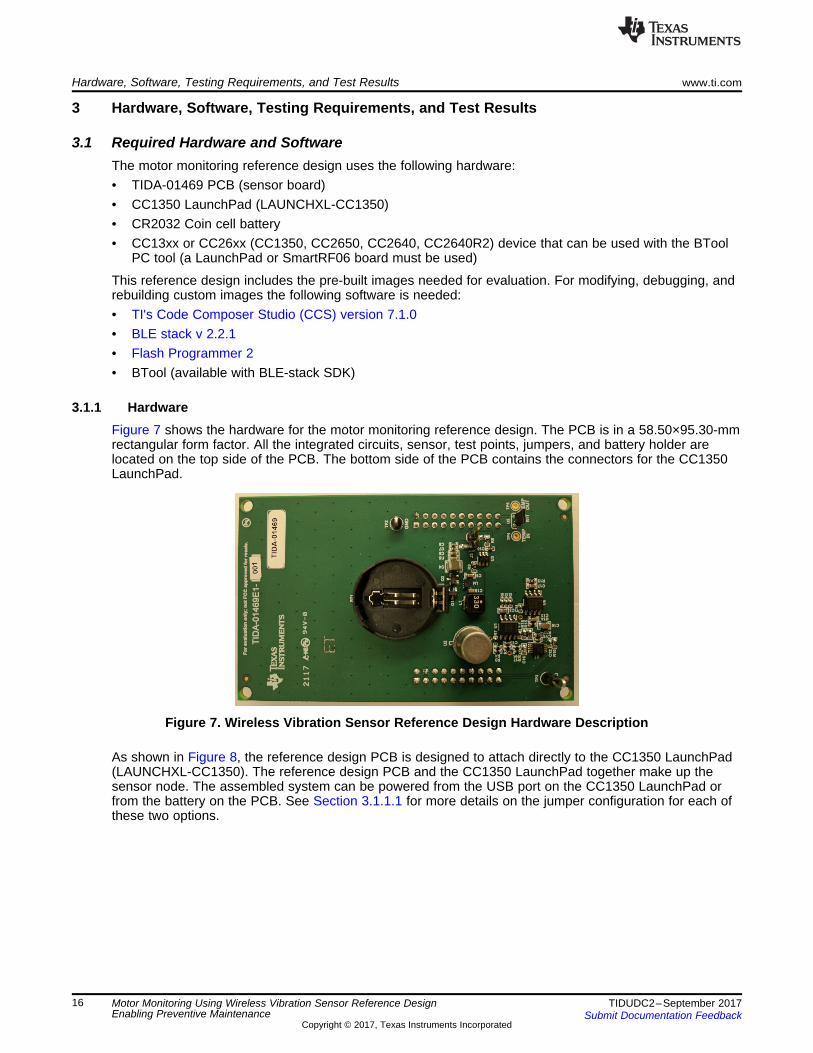
3.1.1 HardwareFigure 7 shows the hardware for the motor monitoring reference design. The PCB is in a 58.50×95.30-mmrectangular form factor. All the integrated circuits, sensor, test points, jumpers, and battery holder arelocated on the top side of the PCB. The bottom side of the PCB contains the connectors for the CC1350LaunchPad.
Figure 7. Wireless Vibration Sensor Reference Design Hardware Description
As shown in Figure 8, the reference design PCB is designed to attach directly to the CC1350 LaunchPad(LAUNCHXL-CC1350). The reference design PCB and the CC1350 LaunchPad together make up thesensor node. The assembled system can be powered from the USB port on the CC1350 LaunchPad orfrom the battery on the PCB. See Section 3.1.1.1 for more details on the jumper configuration for each ofthese two options.

www.ti.com Hardware, Software, Testing Requirements, and Test Results
17TIDUDC2–September 2017Submit Documentation Feedback
Copyright © 2017, Texas Instruments Incorporated
Motor Monitoring Using Wireless Vibration Sensor Reference DesignEnabling Preventive Maintenance
Figure 8. Fully Assembled System
Table 3 lists the assignments of different signals in the reference design PCB to the input/output pins ofthe CC1350 LaunchPad.
Table 3. Pin Assignments When Used with CC1350 LaunchPad
SIGNAL PIN ASSIGNMENTSPI_CLK DIO10SPI_CS DIO21SPI_SDI DIO22LS_INT DIO19
TEMP_IN DIO15TEMP_OUT DIO8
3.1.1.1 Jumper ConfigurationTo properly operate the reference design, the jumpers on the design PCB and the CC1350 LaunchPadmust be installed correctly.
To power the entire system from the CC1350 LaunchPad and enable the onboard emulator configure thejumpers as follows:• TIDA-01469 Board J3 = Opened (disconnects battery from system)• CC1350 LaunchPad P4 = All jumpers on (XDS110 powers CC1350 and TIDA-01469 board, all JTAG
signals connected to CC1350)• CC1350 LaunchPad P10: Set to XDS110 Power (full debug supported)• (Optional) CC1350 LaunchPad P6: Both jumpers on (enables LEDs)
To power the entire system from the coin cell battery and disable the onboard emulator configure thejumpers as follows:• TIDA-01469 Board J3 = Jumper on (connects battery to system)• CC1350 LaunchPad P4 = All jumpers removed (removes XDS power from CC1350 and TIDA-01469
board, disconnects all JTAG signals)• CC1350 LaunchPad P10: Off (removes power from level shifters, disables debug)• (Optional) CC1350 LaunchPad P6: Both jumpers removed (disables LEDs)
3.1.1.2 Test Point DescriptionThis reference design includes several test points to monitor critical signals. The following is a briefdescription of these test points:• TP2, TP3: Ground points for probes or common points for voltage measurements• TP4: Temperature sensor input• TP5: Temperature sensor output

Hardware, Software, Testing Requirements, and Test Results www.ti.com
18 TIDUDC2–September 2017Submit Documentation Feedback
Copyright © 2017, Texas Instruments Incorporated
Motor Monitoring Using Wireless Vibration Sensor Reference DesignEnabling Preventive Maintenance
3.1.1.3 Battery RequirementsOnly insert an Energizer™ CR2032VP lithium battery or battery with equivalent specifications:• CR2032 UL certified battery• Voltage: 3.0 V• Minimum capacity: 240 mAh• Minimum discharge rate: 0.19 mA
NOTE: The battery must be replaced by a trained professional.
3.1.2 Software
3.1.2.1 Compiling FirmwareThe firmware for this reference design is developed using TI's CCS software (version 7.1.0), BLE SDK2.02.01.18, TI-RTOS 2.20.01.08, and ARM Compiler Tools 5.2.6. The instructions in this documentdetailing how to build the firmware assume that CCS and the software packages have been set up andconfigured correctly. For more information on how to set up the development environment, consult theCC2640 BLE Software Developer’s Guide provided in the docs folder of the BLE SDK.
To import the project into CCS:1. Open CCS.2. Click on the Project toolbar.3. Select Import CCS Projects…4. Select the radio option Select archive file.5. Navigate to where the TIDA01469_BLE_Peripheral_App.zip file is installed. If using the default
location, the firmware is at the location, C:\ti\TIDA01469-Firmware.6. Verify that the optionTIDA01469_BLE_Peripheral_Stack is checked.7. Click the Finish button.8. Click on the Project toolbar.9. Select Import CCS Projects…10. Select the radio option Select search-directory.11. Navigate to where the simple_peripheral stack project is located. If using the default location, the
firmware is at the location,C:\ti\simplelink\ble_sdk_2_02_01_18\examples\cc1350lp\simple_peripheral\ccs\stack.
12. Verify that the option simple_peripheral_cc1350lp_stack is checked.13. Click the Finish button.
At this point, the CCS workspace must have both simple_peripheral_cc1350lp_app andsimple_peripheral_cc1350lp_stack projects.
To build the firmware:1. Set the simple_peripheral_cc1350lp_stack project as the active project, and build the project using
Project → Build Project. The generated binary file, simple_peripheral_cc1350lp_stack.hex, is in thesimple_peripheral_cc1350lp_stack/FlashROM folder.
2. Set the simple_peripheral_cc1350lp_app project as the active project, and build the project usingProject → Build Project. The generated binary file, simple_peripheral_cc1350lp_app.hex, is in thesimple_peripheral_cc1350lp_app/FlashROM folder.

www.ti.com Hardware, Software, Testing Requirements, and Test Results
19TIDUDC2–September 2017Submit Documentation Feedback
Copyright © 2017, Texas Instruments Incorporated
Motor Monitoring Using Wireless Vibration Sensor Reference DesignEnabling Preventive Maintenance
3.1.2.2 Loading Firmware on Wireless MCU Using BinariesIncluded in the reference design firmware is a set of pre-built binary images for the application and stack,which can be loaded through the onboard emulator on the CC1350 LaunchPad. Both can be loaded at thesame time. Simply configure the jumpers on the CC1350 LaunchPad to enable the onboard emulator (seeSection 3.1.1.1) and connect a USB cable to the CC1350 LaunchPad. After setting up all the hardware,follow these steps to load the firmware on the sensor and collector using the SmartRF Flash Programmer2:1. Download and install SmartRF Flash Programmer 2 (http://www.ti.com/tool/flash-programmer).2. Open SmartRF Flash Programmer 2.3. In the "Connected devices" window, CC1350 must be listed under XDS110. If it is not listed, check the
USB connection to the CC1350 LaunchPad and click "Refresh" button to rescan for devices. Highlightthe CC1350 device.
4. In the "Main" tab, click the "Multiple" radio button.5. IMPORTANT: In the "Main" tab, under "Actions", click the "All unprotected pages" radio button. This
button erases previous network association information.6. Click on the "Browse" button and navigate to the location of the binary files as described in
Section 3.1.2.1 (see Figure 9).
Figure 9. SmartRF Flash Programmer 2 Configuration
7. Click on the blue circle play button to flash the firmware image onto the sensor. The status bar on thebottom of SmartRF Flash Programmer 2 will show if flashing the image was successful.

Hardware, Software, Testing Requirements, and Test Results www.ti.com
20 TIDUDC2–September 2017Submit Documentation Feedback
Copyright © 2017, Texas Instruments Incorporated
Motor Monitoring Using Wireless Vibration Sensor Reference DesignEnabling Preventive Maintenance
3.1.2.3 Loading Firmware Using CCSFollow these steps to program with CCS:1. Download simple_peripheral_cc1350lp_stack by selecting the simple_peripheral_cc1350lp_stack
project as the active project, and choosing Run → Debug.2. Choose Run → Terminate to stop the debug.3. Download simple_peripheral_cc1350lp_app by selecting the simple_peripheral_cc1350lp_app project
as the active project, and choosing Run → Debug.
NOTE: The preceding steps are needed only for the initial download, and whenever the stackproject is modified. As long as the stack project is not modified, the only required steps are:1. Build the application.2. Download the application.
3.1.2.4 Configuring BToolFollow these steps to set up BTool to act as a central device and communicate with the reference design:
1. Obtain a CC13xx or CC26xx device that can connect to a computer using a USB cable (either aLaunchPad or a SmartRF board) and can run TI's BLE SDK.
2. Plug the device into a computer using the provided USB cable.3. Flash the device with the host_test project, found in the Examples folder of the SDK.4. Run BTool, which can be found in the Tools folder of the SDK.5. In BTool, connect to the correct port corresponding to the device that is connected through USB.
A more detailed description of using BTool can be found in the BTool User's Guide
NOTE: This design guide is written specifically for the CC2640R2 LaunchPad, but very similar stepsare required to use other platforms.
3.1.2.5 Running the FirmwareTo gather motor data, process it, and send it out over a Bluetooth low energy connection, follow thesesteps:1. Disconnect all jumpers from the CC1350 LaunchPad. This prevents the debugging and power interface
of the board from unnecessarily drawing high current when the reference design is running on a coincell battery. See Section 3.1.1.1 for details.
2. Attach the CC1350 LaunchPad to the TIDA-01469 board using four screws and four hex nuts and themounting holes in each corner of both boards. The following parts are used to test this design:• NY PMS 440 0075 PH• NY HN 440
Before using the screws, make sure that the boards are correctly connected using the pin connectors.3. Make sure that a coin cell battery has been inserted into the battery holder. Do not connect the J3
jumper on the design board until the program is ready to start.4. Attach a small magnet to the battery. This magnet couples the reference design to the motor to
accurately detect the vibrations in the motor.5. Connect the J3 jumper on the design board, and use the magnet to attach the reference design to the
motor.6. The program will now begin. For demo purposes, the reference design wakes up after 5 seconds to
take measurements, process the data, and begin sending out Bluetooth low energy advertisements.Every time the reference design goes back into standby, this wake-up interval is the amount of timeafter which the design will wake up to sample data and take the FFT. The code also has an option fora wake-up interval of 8 hours, and any other value can be chosen.

www.ti.com Hardware, Software, Testing Requirements, and Test Results
21TIDUDC2–September 2017Submit Documentation Feedback
Copyright © 2017, Texas Instruments Incorporated
Motor Monitoring Using Wireless Vibration Sensor Reference DesignEnabling Preventive Maintenance
7. Once the device is advertising, the device running BTool can be used to connect to the referencedesign. Follow the BTool User's Guide described in Section 3.1.2.4 for detailed instructions on how todo this.
8. Once connected, BTool can be used to request the desired data from the reference design. Table 4shows what values to write to characteristic 1 to request each block of sample and FFT data.
Table 4. Values for Requesting Data
CHARACTERISTIC 1 VALUE DATA TO REQUEST5D 200 sampled data points5E First 200 FFT points5C Second 200 FFT points5B Third 200 FFT points5A Fourth 200 FFT points59 Fifth 200 FFT points
9. Once notifications have been enabled for characteristic 5 (by writing a value of 1 to characteristic 5'sClient Characteristic Configuration Descriptor), each group of 200 points will be sent to the devicerunning BTool in groups of 20 notifications. The BTool User's Guide describes this process.
10. To tell the design board to go back to standby and wait for the next time to sample data, use BTool towrite any non-zero value to characteristic 3.
3.2 Testing and Results
3.2.1 Test SetupThe Motor Monitoring Using Wireless Vibration Sensor Reference Design has been characterized tosupport all of the critical specifications for this subsystem. The following sections describe the test setupfor these measurements, including the equipment used and the test conditions unless otherwise noted.
3.2.1.1 Power ConsumptionThe power consumption measurements for this reference design are critical in estimating battery life.Measurements of supply current are performed on the reference design hardware.
The majority of the time, the system operates in a very low-power consumption state, often onlyconsuming microamps of current. The test setup for measuring these small currents is illustrated inFigure 10.
The resolution setting of the Agilent 34410A 6½ digit multimeter can place a limit on the amount ofinstantaneous current flowing to the device under test (DUT). This limit can become a problem because atdifferent points during normal operation the current jumps from the microamp range to the milliamp range.For example, when powering on the board, there is an initial inrush of current to the board. Generally, aresolution of 10 mA is enough to prevent any issues with current limits.

+
±ADUT
Agilent34410A
AgilentE3630A Oscilloscope
Tektronix 7104
+
-
+
±
AgilentE3630A
DUT
A
Agilent34410A
Hardware, Software, Testing Requirements, and Test Results www.ti.com
22 TIDUDC2–September 2017Submit Documentation Feedback
Copyright © 2017, Texas Instruments Incorporated
Motor Monitoring Using Wireless Vibration Sensor Reference DesignEnabling Preventive Maintenance
Figure 10. Test Circuit Used for Measuring Small Currents
The system also experiences peaks of high current such as those generated during radio transmission.Measuring these intervals involves using a voltage probe that interfaces to an oscilloscope, which canthen be used to trigger on the high current events. The voltage is measured across a small sense resistor,which allows the current to be calculated. This setup is illustrated in Figure 11.
Figure 11. Test Circuit Used for Measuring Supply Current During High-Peak Currents

+
±
DUTU2-3Agilent
E3630A
TektronixAFG3102
www.ti.com Hardware, Software, Testing Requirements, and Test Results
23TIDUDC2–September 2017Submit Documentation Feedback
Copyright © 2017, Texas Instruments Incorporated
Motor Monitoring Using Wireless Vibration Sensor Reference DesignEnabling Preventive Maintenance
3.2.1.2 Signal Chain TestingThe accelerometer is taken off of this design board so that a function generator could be used to give aknown sine wave input to the AFE. This setup is shown in Figure 12. This test shows that the AFEprovides the correct amplified signal to the ADC, and that the ADC and MCU properly samples the signaland take the FFT. An offset of 1.7 V is used with the function generator to match the reference voltagethat was provided to the accelerometer. An amplitude of 20 mV is used, and the frequency is variedthroughout the range of the reference design (50 Hz to 10 kHz). Because of the output limitations of thefunction generator, a voltage divider is used to get a signal amplitude that is low enough to preventattenuation of the amplified signal.
Figure 12. Setup With Accelerometer Replaced by Function Generator
3.2.1.3 Motor Vibration SensingAn actual industrial motor is used to get motor vibration test data. As described in Section 3.1.2.5, amagnet attached to the battery on the design board couples the reference design to the motor. Figure 13shows the motor, and Figure 14 shows how the reference design is attached to it. Sample and FFT dataare then obtained as described in Section 3.1.2.5.
Figure 13. Motor Setup

Hardware, Software, Testing Requirements, and Test Results www.ti.com
24 TIDUDC2–September 2017Submit Documentation Feedback
Copyright © 2017, Texas Instruments Incorporated
Motor Monitoring Using Wireless Vibration Sensor Reference DesignEnabling Preventive Maintenance
Figure 14. Reference Design Coupled to Motor
3.2.1.4 Wireless RangeThe range of the wireless 2.4-GHz Bluetooth low energy transmission is measured using one CC1350LaunchPad (as part of the reference design) and a Google Pixel with the BLE Scanner app. The referencedesign is set to send out advertisement packets with 100-ms advertising intervals. The phone is thenmoved further away from the reference design and checked to see if the reference design could still beseen advertising. The phone is always in direct sight of the reference design. The distance at whichpackets are no longer received are then measured.

www.ti.com Hardware, Software, Testing Requirements, and Test Results
25TIDUDC2–September 2017Submit Documentation Feedback
Copyright © 2017, Texas Instruments Incorporated
Motor Monitoring Using Wireless Vibration Sensor Reference DesignEnabling Preventive Maintenance
3.2.2 Test Results
NOTE: Unless otherwise noted, the test data in the following sections are measured with the systemat room temperature. All of the measurements in this section are measured with calibratedlab equipment.
3.2.2.1 Power CharacterizationBecause the primary purpose of this reference design is to showcase a battery-powered wireless sensor,characterization of the power consumption of the system is critical.
This reference design remains primarily in the standby state, which is the default state. It is critical that thepower consumption of this state remain as low as possible such that the battery life of the system can bemaximized. In this state, the CC1350 receives power, but will go into its standby mode to minimize powerconsumption. The TPS22860 load switch is turned off to cut off power completely to the op amp, ADC,VREF, and boost converter in the analog input stage.
Table 5 shows the average current consumption of the entire system when it is operating in the standbymode. The current consumption is characterized across different battery voltages. As expected, thecurrent consumption increases at the lower voltage ranges because the internal DC-DC of the CC1350must recharge the bypass capacitors more often to maintain a constant supply voltage. For battery lifecalculations, the average current is calculated over the range of battery voltages from 2.4 to 3.6 V. Theaverage current for standby mode in these voltage ranges is 879.5 nA.
Table 5. Average Current Consumption Across BatteryVoltage in Standby Mode
VBATT (V) AVERAGE SYSTEM CURRENT(nA)
3.6 8013.3 8323.0 8532.8 8852.6 9322.4 974
In addition to the standby state, this reference design consumes varying amounts of power when it isacquiring samples from the ADC, applying the FFT to these samples, sending out Bluetooth low energyadvertisements, and sending out data over a Bluetooth low energy connection. A small sense resistor isused to measure the small amount of current being drawn by the system during each of these periods,and this was confirmed using a digital multimeter. This process is described in Section 3.2.1.1.

Hardware, Software, Testing Requirements, and Test Results www.ti.com
26 TIDUDC2–September 2017Submit Documentation Feedback
Copyright © 2017, Texas Instruments Incorporated
Motor Monitoring Using Wireless Vibration Sensor Reference DesignEnabling Preventive Maintenance
The first state of this reference design after it exits standby mode is sampling data from the ADC throughSPI and performing an FFT on this data. Figure 15 shows the power characterization of the design duringthis state.
Figure 15. ADC Sampling and FFT Power Characterization
The average voltage is 93.31 mV, so dividing by the resistance of the sense resistor gives an averagecurrent of 6.221 mA. This average current is over a period of approximately 109.6 ms. The larger pulsescorrespond to the FFT, and the smaller pulses in between correspond to the ADC sampling through SPI.Only one period is actually performed by this design each time that it wakes up to take data. A loop isused around the ADC sampling and FFT to make it easier to visualize.
www.ti.com Hardware, Software, Testing Requirements, and Test Results
27TIDUDC2–September 2017Submit Documentation Feedback
Copyright © 2017, Texas Instruments Incorporated
Motor Monitoring Using Wireless Vibration Sensor Reference DesignEnabling Preventive Maintenance
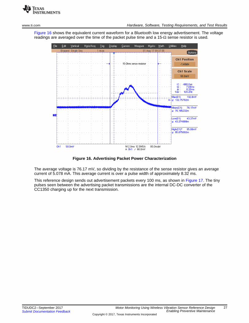
Figure 16 shows the equivalent current waveform for a Bluetooth low energy advertisement. The voltagereadings are averaged over the time of the packet pulse time and a 15-Ω sense resistor is used.
Figure 16. Advertising Packet Power Characterization
The average voltage is 76.17 mV, so dividing by the resistance of the sense resistor gives an averagecurrent of 5.078 mA. This average current is over a pulse width of approximately 8.32 ms.
This reference design sends out advertisement packets every 100 ms, as shown in Figure 17. The tinypulses seen between the advertising packet transmissions are the internal DC-DC converter of theCC1350 charging up for the next transmission.
Hardware, Software, Testing Requirements, and Test Results www.ti.com
28 TIDUDC2–September 2017Submit Documentation Feedback
Copyright © 2017, Texas Instruments Incorporated
Motor Monitoring Using Wireless Vibration Sensor Reference DesignEnabling Preventive Maintenance
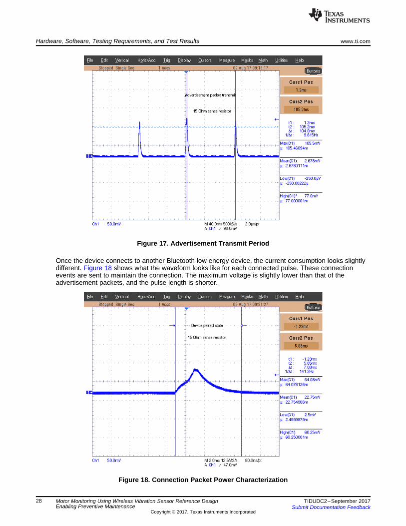
Figure 17. Advertisement Transmit Period
Once the device connects to another Bluetooth low energy device, the current consumption looks slightlydifferent. Figure 18 shows what the waveform looks like for each connected pulse. These connectionevents are sent to maintain the connection. The maximum voltage is slightly lower than that of theadvertisement packets, and the pulse length is shorter.
Figure 18. Connection Packet Power Characterization

www.ti.com Hardware, Software, Testing Requirements, and Test Results
29TIDUDC2–September 2017Submit Documentation Feedback
Copyright © 2017, Texas Instruments Incorporated
Motor Monitoring Using Wireless Vibration Sensor Reference DesignEnabling Preventive Maintenance
The average voltage is 22.755 mV, so dividing by the resistance of the sense resistor gives an averagecurrent of 1.517 mA. This average current is over a pulse width of approximately 7.08 ms. Figure 19shows the period of the device when it is in a connection. The connection interval is 100 ms.
Figure 19. Connection Packet Transmit Period
Figure 20 shows the power characterization of notification pulse. Each pulse corresponds to thetransmission of 20 bytes of data in a single notification.
Figure 20. Notification Power Characterization

( ) ( )( ) ( ) ( ) ( ) ( ) ( ) ( ) ( )mA s mA s mA s mA s
S tandby S tandby Sampling Sampling Advertising Advertising Data Data
(s)Total
Battery Capacity mAh 1 yearBattery Lifetime yr Derating Factor
8760 hoursI t I FFT t FFT I t I t
t
= ´ ´æ ö´ ´ + ´ + + ´ ´ç ÷ç ÷è ø
Hardware, Software, Testing Requirements, and Test Results www.ti.com
30 TIDUDC2–September 2017Submit Documentation Feedback
Copyright © 2017, Texas Instruments Incorporated
Motor Monitoring Using Wireless Vibration Sensor Reference DesignEnabling Preventive Maintenance
For BTool to be able to process the notifications before filling its buffer, a delay is required between eachnotifications. A 20-ms delay is used, so one of these pulses are seen every 20 ms, meaning there are fivepulses for each connection period.
3.2.2.2 Battery Life CalculationsThe main parameters that affect the estimated battery life of the entire system are:• Capacity rating of the battery• Average standby-state current consumption• Standby-state duration• Average sampling and FFT current consumption• Sampling and FFT duration• Average advertising packet current consumption• Advertising duration• Average connection and data transmission current consumption• Connection and data transmission duration
Equation 9 describes the estimated battery life of the system.
(9)
Because this design involves a connection being established between two devices and data being sentover that connection, the exact timing with which the connection is established and data is requestedaffects exactly how long the reference design operates in each power consumption state. For the batterycalculations of the device, the following assumptions are made:• An 8-hour interval is used between wakeup events. This interval is the amount of time that the
reference design is in standby mode before waking up to sample data.• A connection is established after one advertisement packet is received by the central device.• 1000 points of FFT data are sent in five groups that each consisted of 20 10-sample notifications.• After receiving all of the data, the central device immediately sends a byte to the reference design,
indicating that the design must go back into standby mode and wait for the next wakeup event.
With these assumptions considered, Equation 9 can be used to calculate the battery life as 25.112 years.
Table 6 and Figure 21 show the battery life estimates for wakeup intervals ranging from 8 hours down to10 minutes. This is important because, although larger intervals are more useful for low-power periodicmonitoring, a smaller interval may be desired when a motor is showing minor signs of damage so thatmore frequent monitoring can detect when the damage warrants maintenance.
Table 6. Battery Lifetime versus Wakeup Period
WAKEUP PERIOD (MIN) BATTERY LIFE (YEARS)480 25.112064790240 23.248417910120 20.24431778060 16.08842236030 11.40863887020 8.84032514810 5.281879421
Sample
Dat
a V
alue
0 50 100 150 200 250 300 350 40010000
15000
20000
25000
30000
35000
D001 Frequency (× 10 = Hz)
Dat
a
0 200 400 600 800 1000 12000
5000
10000
15000
20000
D002
Wakeup Period (min)
Bat
tery
Life
(ye
ars)
0 50 100 150 200 250 300 350 400 450 5003
6
9
12
15
18
21
24
27
D006
www.ti.com Hardware, Software, Testing Requirements, and Test Results
31TIDUDC2–September 2017Submit Documentation Feedback
Copyright © 2017, Texas Instruments Incorporated
Motor Monitoring Using Wireless Vibration Sensor Reference DesignEnabling Preventive Maintenance
Figure 21. Battery Lifetime versus Wakeup Period
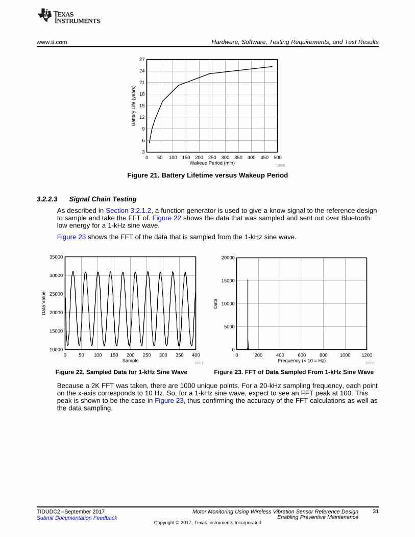
3.2.2.3 Signal Chain TestingAs described in Section 3.2.1.2, a function generator is used to give a know signal to the reference designto sample and take the FFT of. Figure 22 shows the data that was sampled and sent out over Bluetoothlow energy for a 1-kHz sine wave.
Figure 23 shows the FFT of the data that is sampled from the 1-kHz sine wave.
Figure 22. Sampled Data for 1-kHz Sine Wave Figure 23. FFT of Data Sampled From 1-kHz Sine Wave
Because a 2K FFT was taken, there are 1000 unique points. For a 20-kHz sampling frequency, each pointon the x-axis corresponds to 10 Hz. So, for a 1-kHz sine wave, expect to see an FFT peak at 100. Thispeak is shown to be the case in Figure 23, thus confirming the accuracy of the FFT calculations as well asthe data sampling.

Sample
Dat
a
0 50 100 150 200 250 300 350 4000
5000
10000
15000
20000
25000
30000
35000
D007 Frequency (× 10 = Hz)
Dat
a
0 200 400 600 800 1000 12000
20000
40000
60000
80000
D005
Sample
Dat
a
0 50 100 150 200 250 300 350 40015000
20000
25000
30000
35000
D003Frequency (× 10 = Hz)
Dat
a
0 200 400 600 800 1000 12000
5000
10000
15000
20000
25000
D004
Hardware, Software, Testing Requirements, and Test Results www.ti.com
32 TIDUDC2–September 2017Submit Documentation Feedback
Copyright © 2017, Texas Instruments Incorporated
Motor Monitoring Using Wireless Vibration Sensor Reference DesignEnabling Preventive Maintenance
This process is repeated for a 5-kHz sine wave. The results are shown in Figure 24 and Figure 25.
Figure 24. Sampled Data for 5-kHz Sine Wave Figure 25. FFT of Data Sampled From 5-kHz Sine Wave
As described for the 1-kHz sine wave, each point on the x-axis for the FFT corresponds to 10 Hz, soexpect to see a peak at 500. This is the case here, again confirming the accuracy of the sampling andFFT calculation. The sampled data plot shows less resolution than it did for the 1-kHz sine wave becausethe signal frequency is closer to the sampling frequency, but the FFT is still able to identify the frequencycorrectly.
3.2.2.4 Motor Vibration SensingThe sampled data from the motor setup is shown in Figure 26.
The periodicity of the data can be seen. Because of the multiple present frequencies, only 400 points areshown to increase readability. The FFT generated from this data is shown in Figure 27.
Figure 26. Motor Setup Sampled Data Figure 27. FFT From Motor Setup Sampled Data
Multiple FFT peaks can be seen, which correspond to the multiple harmonics that are present in an actualmotor setup. Spectral data generated by the software that is driving the motor is compared to this FFTdata to confirm the accuracy of the reference design's sampling and FFT calculation.

www.ti.com Hardware, Software, Testing Requirements, and Test Results
33TIDUDC2–September 2017Submit Documentation Feedback
Copyright © 2017, Texas Instruments Incorporated
Motor Monitoring Using Wireless Vibration Sensor Reference DesignEnabling Preventive Maintenance
3.2.2.5 Wireless RF RangeThe wireless RF range is measured to be about 72 meters in a typical office environment with a direct lineof sight. The transmit power is set to 0 dBm, which is the default used by the Bluetooth low energy SDK.Radio performance varies in the end-equipment environment because of the number of obstructions in theRF transmit path reduces range. For full verification of the hardware transmitting characteristics of thisreference design, further testing with end-equipment context is required.

Design Files www.ti.com
34 TIDUDC2–September 2017Submit Documentation Feedback
Copyright © 2017, Texas Instruments Incorporated
Motor Monitoring Using Wireless Vibration Sensor Reference DesignEnabling Preventive Maintenance
4 Design Files
4.1 SchematicsTo download the schematics, see the design files at TIDA-01469.
4.2 Bill of MaterialsTo download the bill of materials (BOM), see the design files at TIDA-01469.
4.3 PCB Layout Recommendations
4.3.1 Layout PrintsTo download the layer plots, see the design files at TIDA-01469.
4.4 Altium ProjectTo download the Altium project files, see the design files at TIDA-01469.
4.5 Gerber FilesTo download the Gerber files, see the design files at TIDA-01469.
4.6 Assembly DrawingsTo download the assembly drawings, see the design files at TIDA-01469.
5 Software FilesTo download the software files, see the design files at TIDA-01469.
6 Related Documentation
1. Texas Instruments, Reverse Current/Battery Protection Circuits, Application Report (SLVA139)2. Texas Instruments, Coin cells and peak current draw, White Paper (SWRA349)
6.1 TrademarksSimpleLink, LaunchPad, MSP430, SmartRF, Code Composer Studio, TINA-TI are trademarks of TexasInstruments.ARM, Cortex are registered trademarks of ARM Ltd.Bluetooth is a registered trademark of Bluetooth SIG.ULPBench is a trademark of Embedded Microprocessor Benchmark Consortium.CoreMark is a registered trademark of Embedded Microprocessor Benchmark Consortium.Energizer is a trademark of Energizer Brands, LLC.IAR Embedded Workbench is a registered trademark of IAR Systems AB.IEEE is a registered trademark of IEEE.IMI Sensors is a registered trademark of PCB Group, Inc.All other trademarks are the property of their respective owners.

www.ti.com About the Authors
35TIDUDC2–September 2017Submit Documentation Feedback
Copyright © 2017, Texas Instruments Incorporated
Motor Monitoring Using Wireless Vibration Sensor Reference DesignEnabling Preventive Maintenance
7 About the AuthorsNATHAN SIEGEL is a systems designer at Texas Instruments, where he is responsible for developingreference design solutions for the industrial segment. Nathan earned his bachelor of science (BS) inelectrical engineering from the University of California, Los Angeles (UCLA).
GUSTAVO MARTINEZ is a senior systems architect at Texas Instruments where he is responsible fordeveloping reference designs for industrial applications. Gustavo has ample experience developingsystem reference designs for the Smart Grid and home automation segments, which include highperformance application processors, floating-point digital signal processors, and RF technology. Gustavoobtained his master of electrical engineering degree from the University of Houston and his bachelor ofscience in electrical engineering degree from the University of Texas at El Paso.

IMPORTANT NOTICE FOR TI DESIGN INFORMATION AND RESOURCES
Texas Instruments Incorporated (‘TI”) technical, application or other design advice, services or information, including, but not limited to,reference designs and materials relating to evaluation modules, (collectively, “TI Resources”) are intended to assist designers who aredeveloping applications that incorporate TI products; by downloading, accessing or using any particular TI Resource in any way, you(individually or, if you are acting on behalf of a company, your company) agree to use it solely for this purpose and subject to the terms ofthis Notice.TI’s provision of TI Resources does not expand or otherwise alter TI’s applicable published warranties or warranty disclaimers for TIproducts, and no additional obligations or liabilities arise from TI providing such TI Resources. TI reserves the right to make corrections,enhancements, improvements and other changes to its TI Resources.You understand and agree that you remain responsible for using your independent analysis, evaluation and judgment in designing yourapplications and that you have full and exclusive responsibility to assure the safety of your applications and compliance of your applications(and of all TI products used in or for your applications) with all applicable regulations, laws and other applicable requirements. Yourepresent that, with respect to your applications, you have all the necessary expertise to create and implement safeguards that (1)anticipate dangerous consequences of failures, (2) monitor failures and their consequences, and (3) lessen the likelihood of failures thatmight cause harm and take appropriate actions. You agree that prior to using or distributing any applications that include TI products, youwill thoroughly test such applications and the functionality of such TI products as used in such applications. TI has not conducted anytesting other than that specifically described in the published documentation for a particular TI Resource.You are authorized to use, copy and modify any individual TI Resource only in connection with the development of applications that includethe TI product(s) identified in such TI Resource. NO OTHER LICENSE, EXPRESS OR IMPLIED, BY ESTOPPEL OR OTHERWISE TOANY OTHER TI INTELLECTUAL PROPERTY RIGHT, AND NO LICENSE TO ANY TECHNOLOGY OR INTELLECTUAL PROPERTYRIGHT OF TI OR ANY THIRD PARTY IS GRANTED HEREIN, including but not limited to any patent right, copyright, mask work right, orother intellectual property right relating to any combination, machine, or process in which TI products or services are used. Informationregarding or referencing third-party products or services does not constitute a license to use such products or services, or a warranty orendorsement thereof. Use of TI Resources may require a license from a third party under the patents or other intellectual property of thethird party, or a license from TI under the patents or other intellectual property of TI.TI RESOURCES ARE PROVIDED “AS IS” AND WITH ALL FAULTS. TI DISCLAIMS ALL OTHER WARRANTIES ORREPRESENTATIONS, EXPRESS OR IMPLIED, REGARDING TI RESOURCES OR USE THEREOF, INCLUDING BUT NOT LIMITED TOACCURACY OR COMPLETENESS, TITLE, ANY EPIDEMIC FAILURE WARRANTY AND ANY IMPLIED WARRANTIES OFMERCHANTABILITY, FITNESS FOR A PARTICULAR PURPOSE, AND NON-INFRINGEMENT OF ANY THIRD PARTY INTELLECTUALPROPERTY RIGHTS.TI SHALL NOT BE LIABLE FOR AND SHALL NOT DEFEND OR INDEMNIFY YOU AGAINST ANY CLAIM, INCLUDING BUT NOTLIMITED TO ANY INFRINGEMENT CLAIM THAT RELATES TO OR IS BASED ON ANY COMBINATION OF PRODUCTS EVEN IFDESCRIBED IN TI RESOURCES OR OTHERWISE. IN NO EVENT SHALL TI BE LIABLE FOR ANY ACTUAL, DIRECT, SPECIAL,COLLATERAL, INDIRECT, PUNITIVE, INCIDENTAL, CONSEQUENTIAL OR EXEMPLARY DAMAGES IN CONNECTION WITH ORARISING OUT OF TI RESOURCES OR USE THEREOF, AND REGARDLESS OF WHETHER TI HAS BEEN ADVISED OF THEPOSSIBILITY OF SUCH DAMAGES.You agree to fully indemnify TI and its representatives against any damages, costs, losses, and/or liabilities arising out of your non-compliance with the terms and provisions of this Notice.This Notice applies to TI Resources. Additional terms apply to the use and purchase of certain types of materials, TI products and services.These include; without limitation, TI’s standard terms for semiconductor products http://www.ti.com/sc/docs/stdterms.htm), evaluationmodules, and samples (http://www.ti.com/sc/docs/sampterms.htm).
Mailing Address: Texas Instruments, Post Office Box 655303, Dallas, Texas 75265Copyright © 2017, Texas Instruments Incorporated