mp26123 2a,24v input, 600khz 2/3-cell switching li-ion
TRANSCRIPT

MP26123 2A,24V Input, 600kHz 2/3-Cell Switching Li-ion Battery Charger
MP26123 Rev. 1.01 www.MonolithicPower.com 1 10/28/2011 MPS Proprietary Information. Patent Protected. Unauthorized Photocopy and Duplication Prohibited. © 2011 MPS. All Rights Reserved.
The Future of Analog IC Technology
DESCRIPTION The MP26123 is a monolithic DC-DC step-down switching charger for 2- or 3-cell Li-ion battery packs. It has an integrated high-side power MOSFET can output up to a 2A charge current. It also has peak-current–mode control for fast loop response and easy compensation.
The MP26123 uses a sense resistor to control a programmable charge current, and accurately regulates the charge current and charge voltage using two control loops.
The MP26123 has multiple fault condition protections that include cycle-by-cycle current limiting and thermal shutdown. Other safety features include battery temperature monitoring and protection, charge status indication and programmable timer to cease the charging cycle when timer out.
The MP26123 requires a minimal number of readily-available external components.
The MP26123 is available in a 4mm x 4mm 16-pin QFN package.
FEATURES
Charges 2- or 3-Cell Li-Ion Battery Packs Wide Operating Input Range Programmable Charging Current of up to 2A ±0.75% VBATT Accuracy 0.2Ω Integrated Power MOSFET Up to 90% Efficiency Fixed 600kHz Frequency Preconditioning for Fully Depleted Batteries Charging Status Indicator Input Supply Fault Indicator Thermal Shutdown Cycle-by-Cycle Over-Current Protection Battery Temperature Monitor and Protection
APPLICATIONS Mobile Internet Device Portable Media Player Netbook Charger for 2- or 3-Cell Li-Ion Batteries Distributed Power Systems
For MPS green status, please visit MPS website under Quality Assurance.“MPS” and “The Future of Analog IC Technology” are Registered Trademarks of Monolithic Power Systems, Inc.
TYPICAL APPLICATION

MP26123 – 2A, 24V INPUT, 600kHz 2-3 CELL SWITCHING LI-ION BATTERY CHARGER
MP26123 Rev. 1.01 www.MonolithicPower.com 2 10/28/2011 MPS Proprietary Information. Patent Protected. Unauthorized Photocopy and Duplication Prohibited. © 2011 MPS. All Rights Reserved.
ORDERING INFORMATION Part Number* Package Top Marking Free Air Temperature (TA) MP26123DR QFN16 (4x4mm) M26123 -40°C to +85°C
*For Tape & Reel, add suffix –Z (e.g. MP26123DR–Z)
For RoHS compliant packaging, add suffix –LF (e.g. MP MP26123DR–LF–Z)
PACKAGE REFERENCE TOP VIEW
EXPOSED PADON BACKSIDE
PIN 1 ID
VCC
NTC
ACOK
CHGOK
GND
CSP
BATT
COMPI
1
2
3
4
13141516
8765
COMPVCELLSENVREF33
TMRBSTSWVIN
12
11
10
9
ABSOLUTE MAXIMUM RATINGS (1) Supply Voltage VCC, VIN ............................ 26V VSW..................................... -0.3V to (VIN + 0.3V) VBST ...................................................... VSW + 6V VCSP, VBATT, ...................................-0.3V to +18V VACOK, VCHGOK, ..............................-0.3V to +26V All Other Pins..................................-0.3V to +6V
Continuous Power Dissipation (TA = 25°C) (2)
............................................................. 2.7W Junction Temperature...............................150°C Lead Temperature ....................................260°C Storage Temperature............... -65°C to +150°C
Recommended Operating Conditions (3) Supply Voltage VIN ..............................9V to 24V Maximum Junction Temp. (TJ) ..................125°C
Thermal Resistance (4) θJA θJC QFN16 (4x4mm)..................... 46 ...... 10... °C/W
Notes: 1) Exceeding these ratings may damage the device. 2) The maximum allowable power dissipation is a function of the
maximum junction temperature TJ(MAX), the junction-to-ambient thermal resistance θJA, and the ambient temperature TA. The maximum allowable continuous power dissipation at any ambient temperature is calculated by PD(MAX)=(TJ(MAX)-TA)/θJA. Exceeding the maximum allowable power dissipation will cause excessive die temperature, and the regulator will go into thermal shutdown. Internal thermal shutdown circuitry protects the device from permanent damage.
3) The device is not guaranteed to function outside of its operating conditions.
4) Measured on JESD51-7 4-layer board.

MP26123 – 2A, 24V INPUT, 600kHz 2-3 CELL SWITCHING LI-ION BATTERY CHARGER
MP26123 Rev. 1.01 www.MonolithicPower.com 3 10/28/2011 MPS Proprietary Information. Patent Protected. Unauthorized Photocopy and Duplication Prohibited. © 2011 MPS. All Rights Reserved.
ELECTRICAL CHARACTERISTICS VIN = 19V, TA = 25°C, CELLS=0V, unless otherwise noted.
Parameters Symbol Condition Min Typ Max Units
CELLS=0V 8.337 8.4 8.463Terminal battery voltage VBATT
CELLS=Float 12.505 12.6 12.695V
CSP,BATT current ICSP,IBATT Charging disabled 1 µA
Switch on resistance RDS(ON) 0.2 Ω
Switch leakage EN= 4V, VSW = 0V 0 1 μA
CC(5) 4.1 A Peak current limit
TRICKLE 2 A
CC current ICC RS1=100mΩ 1.8 2.0 2.2 A
Trickle charge current ITRICKLE 10% ICC
Trickle charge voltage threshold VTC 3 V/cell
Trickle charge hysteresis 350 mV
Termination current threshold IBF 5% 10% 15% ICC
Oscillator frequency fSW CELLS=0V, VBATT =7V
600 kHz
Fold-back frequency VBATT =0V 190 kHz
Maximum duty cycle 90 %
Maximum current sense voltage (CSP to BATT)
VSENSE 170 200 230 mV
Minimum on time (5) tON 100 ns
Under-voltage lockout threshold rising
3 3.2 3.4 V
Under-voltage lockout threshold hysteresis
200 1000 mV
Open-drain sink current VDRAIN =0.3V 5 mA
Dead battery indicator In trickle mode CTMR=0.1μF
30 min
Recharge threshold at VBATT VRECHG 4.0 V/cell
Recharge hysteresis 100 mV
NTC low-temp rising threshold RNTC=NCP18X103, 0°C 70.5 73.5 76.5 %of
VREF33
NTC high-temp falling threshold RNTC=NCP18X103, 50°C
27.5 29.5 31.5 %of
VREF33
VIN min head-room (reverse blocking)
VIN−VBATT 180 mV

MP26123 – 2A, 24V INPUT, 600kHz 2-3 CELL SWITCHING LI-ION BATTERY CHARGER
MP26123 Rev. 1.01 www.MonolithicPower.com 4 10/28/2011 MPS Proprietary Information. Patent Protected. Unauthorized Photocopy and Duplication Prohibited. © 2011 MPS. All Rights Reserved.
ELECTRICAL CHARACTERISTICS (continued) VIN = 19V, TA = 25°C, CELLS=0V, unless otherwise noted.
Parameters Symbol Condition Min Typ Max Units
EN input low voltage 0.4 V
EN input high voltage 1.8 V
EN=4V 4 EN input current
EN=0V 0.2 μA
EN =4V 0.5 mA
Supply current (shutdown) EN =4V, Consider VREF33 pin output current, R3=10k,RNTC=10k
0.665 mA
Supply current (quiescent) EN =0V, CELLS=0V 2.0 mA
Thermal shutdown (5) 150 °C
VREF33 output voltage 3.3 V
VREF33 load regulation ILOAD =0 to 10mA 30 mV
Notes: 5) Guaranteed by design.

MP26123 – 2A, 24V INPUT, 600kHz 2-3 CELL SWITCHING LI-ION BATTERY CHARGER
MP26123 Rev. 1.01 www.MonolithicPower.com 5 10/28/2011 MPS Proprietary Information. Patent Protected. Unauthorized Photocopy and Duplication Prohibited. © 2011 MPS. All Rights Reserved.
PIN FUNCTIONS Pin # Name Description
1 VCC IC supply voltage.
2 NTC Thermistor Input. Connect a resistor from this pin to VREF33, and the thermistor from this pin to ground.
3 ACOK Valid Input Supply Indicator. Open drain output. Add pull-up resistor. Logic LOW indicates the presence of a valid input supply.
4 CHGOK Charging Status Indicator. Open drain output. Add pull-up resistor. Logic LOW indicates normal charging. Logic HIGH indicates either a completed charge process or suspendedprocess because of some fault.
5 VREF33 Internal Linear Regulator, 3.3V Reference Output. Bypass to GND with a 1μF ceramic capacitor.
6 EN On/Off Control Input.
7 CELLS Command Input for the Number of Li-ion Cells. Connect to VREF33 or float for 3-cell operation. Ground for 2-cell operation.
8 COMPV V-LOOP Compensation. Decouple this pin with a capacitor and a resistor.
9 COMPI I-LOOP Compensation. Decouple this pin with a capacitor and a resistor.
10 BATT Positive Battery Terminal.
11 CSP
Battery-Charge Current-Sense–Positive Input. Connect a resistor RS1 between CSP and
BATT. The full charge current is: mΩRS1
200mVAICHG .
12 GND Ground. This pin is the voltage reference for the regulated output voltage. This node should be placed outside of the switching diode (D2) to the input ground path to prevent switching current spikes from inducing voltage noise into the part.
13 TMR Set Safe Timer Period. 0.1µA current charges and discharges the external capacitor decoupled to GND. The capacitor value programs the timer period.
14 BST Bootstrap. Requires a charged capacitor to drive the power switch’s gate above the supply voltage. Connect a capacitor between SW and BST pins to form a floating supply across the power switch driver.
15 SW Switch Output.
16 VIN Regulator Input Voltage. The MP26123 regulates a 9V-to-24V input to a voltage suitable for charging either a 2- or 3-cell Li-ion battery. Requires capacitors to prevent large voltage spikes from appearing at the input.

MP26123 – 2A, 24V INPUT, 600kHz 2-3 CELL SWITCHING LI-ION BATTERY CHARGER
MP26123 Rev. 1.01 www.MonolithicPower.com 6 10/28/2011 MPS Proprietary Information. Patent Protected. Unauthorized Photocopy and Duplication Prohibited. © 2011 MPS. All Rights Reserved.
TYPICAL PERFORMANCE CHARACTERISTICS VIN=19V, C1=4.7μF, C2=22μF, L=4.7μH, RS1=100mΩ, Real/Simulation Battery Load, TA=25°C, unless otherwise noted.

MP26123 – 2A, 24V INPUT, 600kHz 2-3 CELL SWITCHING LI-ION BATTERY CHARGER
MP26123 Rev. 1.01 www.MonolithicPower.com 7 10/28/2011 MPS Proprietary Information. Patent Protected. Unauthorized Photocopy and Duplication Prohibited. © 2011 MPS. All Rights Reserved.
TYPICAL PERFORMANCE CHARACTERISTICS (continued) VIN=19V, C1=4.7μF, C2=22μF, L=4.7μH, RS1=100mΩ, Real/Simulation Battery Load, TA=25°C, unless otherwise noted.

MP26123 – 2A, 24V INPUT, 600kHz 2-3 CELL SWITCHING LI-ION BATTERY CHARGER
MP26123 Rev. 1.01 www.MonolithicPower.com 8 10/28/2011 MPS Proprietary Information. Patent Protected. Unauthorized Photocopy and Duplication Prohibited. © 2011 MPS. All Rights Reserved.
TYPICAL PERFORMANCE CHARACTERISTICS (continued) VIN=19V, C1=4.7μF, C2=22μF, L=4.7μH, RS1=100mΩ, Real/Simulation Battery Load, TA=25°C, unless otherwise noted.

MP26123 – 2A, 24V INPUT, 600kHz 2-3 CELL SWITCHING LI-ION BATTERY CHARGER
MP26123 Rev. 1.01 www.MonolithicPower.com 9 10/28/2011 MPS Proprietary Information. Patent Protected. Unauthorized Photocopy and Duplication Prohibited. © 2011 MPS. All Rights Reserved.
FUNCTIONAL BLOCK DIAGRAM
Figure 1—Functional Block Diagram

MP26123 – 2A, 24V INPUT, 600kHz 2-3 CELL SWITCHING LI-ION BATTERY CHARGER
MP26123 Rev. 1.01 www.MonolithicPower.com 10 10/28/2011 MPS Proprietary Information. Patent Protected. Unauthorized Photocopy and Duplication Prohibited. © 2011 MPS. All Rights Reserved.
OPERATION The MP26123 is a peak-current–mode controlled switching charger for use with Li-ion batteries.
At the beginning of a cycle, M1 is off, and the COMP voltage is higher than the output of current sense amplifer, A1. The PWM comparator’s output is low, and the rising edge of the 600kHz CLK signal sets the RS flip-flop, which turns on M1, thus connecting the SW pin and the inductor to the input supply.
As the inductor current increases, the output of A1 increases. While the sum of A1’s output and the slope compensation remains below the COMP voltage, the falled edge of the CLK resets the RS flip-flop. When this signal exceeds the COMP voltage, the RS flip-flop resets and turns M1 off. The external switching diode D2 then conducts the inductor current.
The MP26123 uses COMP to select the smaller value of GMI and GMV to implement either current loop control or voltage loop control. Current loop control occurs when the battery voltage is low, which results in the saturation of the GMV output. GMI compares the charge current (as a voltage sensed through RS1) against the reference voltage to regulate the charge current to a constant value. When the battery voltage charges up to the reference voltage, the output of GMV goes low and initiates voltage loop control to control the duty cycle to regulate the output voltage.
The MP26123 has an internal linear regulator—VREF33—to power internal circuitry. It can also power external circuitry as long as the load does not exceed the maximum current (30mA). Connect a 1μF bypass capacitor from VREF33 to GND to ensure stability.
Charge Cycle (Mode change: Trickle CC CV)
At the start of a charging cycle, the MP26123 monitors VBATT. If VBATT is lower than the trickle-charge threshold, VTC (typically 3.0V/cell), the charging cycle will start in “trickle-charge mode” (10% of the RS1 programmed constant-charge current, ICC) until the battery voltage reaches VTC.
If the charge stays in the “trickle-charging mode” until “time out” condition is triggered, charging terminates and will not resume until the input power or EN signal refreshes. Otherwise, GMI regulates the charge current to the level set by RS1. The charger is operating at “constant current charging mode.” The duty cycle of the switcher is determined by the COMPI voltage that is regulated by the amplifier GMI.
When the battery voltage reaches constant-voltage–mode threshold, GMV regulates the COMP pin and the duty cycle for constant voltage mode. When the charge current drops to the battery-full threshold, IBF (typical 10% CC), the battery is defined as fully charged, the charger stops charging, and CHGOK goes high to indicate the charge-full condition. If the total charge time exceeds the timer period, the charging terminates at once and will resume when either the input power or EN signal can restart the charger.
Figure 2 shows the typical charge profile of MP26123.
Figure 2—Li-Ion Battery Charge Profile

MP26123 – 2A, 24V INPUT, 600kHz 2-3 CELL SWITCHING LI-ION BATTERY CHARGER
MP26123 Rev. 1.01 www.MonolithicPower.com 11 10/28/2011 MPS Proprietary Information. Patent Protected. Unauthorized Photocopy and Duplication Prohibited. © 2011 MPS. All Rights Reserved.
Automatic Recharge After the battery has completely recharged, the charger disables all blocks except the battery voltage monitor to limit leakage current. If the battery voltage falls below 4.0V/Cell, the chip will begin recharging using soft-start. The timer will then reset to avoid timer-related charging disruptions.
Charger Status Indication MP26123 has two open-drain status outputs:
ACOK and CHGOK . The ACOK pin goes low when the IC supply voltage VCC exceeds the under-voltage lockout threshold and the regulated voltage VIN is 300mV higher than VBATT to make sure the regulator can operate normally.
CHGOK indicates charge status. Table 1
describes ACOK and CHGOK outputs under different charge conditions.
Table 1―Charging Status Indication
ACOK CHGOK Charger Status
low low In charging
low high End of charge, NTC fault, timer out, thermal
shutdown, EN disable
high high VIN –VBATT<0.3V. VCC<UVLO,
Timer Operation
MP26123 uses the internal timer to limit the charge period during trickle charge and total charge cycle. Once the charge time exceeds the time limit the MP26123 terminates charging. A good battery should fully recharge within the allotted time period; otherwise the battery has a fault. An external capacitor at the TMR pin programs the time period.
The trickle mode charge time is:
TMRTRICKLE _ TMR
CT 30mins
0.1 F
The total charge time is:
TMRTOTAL _ TMR
CT 3hours
0.1 F
When time-out occurs, charger is suspended. And only refresh the input power or EN signal or
auto-recharge (The event that VBATT falls through 4V/cell) can restart the charge cycle.
Negative Thermal Coefficient (NTC) Thermistor The MP26123 has a built-in NTC-resistance window comparator that allows the MP26123 to sense the battery temperature through the thermistor included in the battery pack. Connect a resistor with an appropriate value from VREF33 to the NTC pin, and connect the thermistor from the NTC pin to GND. A resistor divider determines the voltage on the NTC pin as a function of the battery temperature. Charging halts when the NTC voltage falls below the lower NTC window threshold. Charging resumes when the voltage is within the NTC window range.
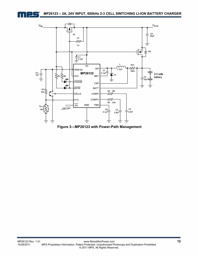
Power Path Management MP26123 is a stand-alone switching charger. Typically, the regulated input voltage VIN receives power from the adapter input, VIN, through a diode that blocks the battery voltage to VCC. For power path application, however, VIN powers the system and charges the battery simultaneously so the user can start-up a device with a drained battery when it is connected to an adapter. Replace the diode from the stand-alone switching charger circuit with a MOSFET to improve system efficiency and reduce voltage drop of the block device.
An additional MOSFET between VIN and the battery allows the battery to charge even in the absence of an adapter or connection to an invalid adapter. Figure 3 shows a typical application circuit with power-path management. When the adapter input is invalid or absent, the block diode
is replaced by a MOSFET controlled by ACOK signal.
MP26123 – 2A, 24V INPUT, 600kHz 2-3 CELL SWITCHING LI-ION BATTERY CHARGER
MP26123 Rev. 1.01 www.MonolithicPower.com 12 10/28/2011 MPS Proprietary Information. Patent Protected. Unauthorized Photocopy and Duplication Prohibited. © 2011 MPS. All Rights Reserved.
D2
R6
10k
Figure 3—MP26123 with Power-Path Management

MP26123 – 2A, 24V INPUT, 600kHz 2-3 CELL SWITCHING LI-ION BATTERY CHARGER
MP26123 Rev. 1.01 www.MonolithicPower.com 13 10/28/2011 MPS Proprietary Information. Patent Protected. Unauthorized Photocopy and Duplication Prohibited. © 2011 MPS. All Rights Reserved.
OPERATION FLOW CHART
Figure 4— Normal Charging Operation Flow Chart

MP26123 – 2A, 24V INPUT, 600kHz 2-3 CELL SWITCHING LI-ION BATTERY CHARGER
MP26123 Rev. 1.01 www.MonolithicPower.com 14 10/28/2011 MPS Proprietary Information. Patent Protected. Unauthorized Photocopy and Duplication Prohibited. © 2011 MPS. All Rights Reserved.
OPERATION FLOW CHART (continued)
Figure 5—Fault Protection Flow Chart

MP26123 – 2A, 24V INPUT, 600kHz 2-3 CELL SWITCHING LI-ION BATTERY CHARGER
MP26123 Rev. 1.01 www.MonolithicPower.com 15 10/28/2011 MPS Proprietary Information. Patent Protected. Unauthorized Photocopy and Duplication Prohibited. © 2011 MPS. All Rights Reserved.
APPLICATION INFORMATION Setting the Charge Current The charge current of MP26123 is set by the sense resistor RS1 (See Typical Application), and determined with the following equation:
mΩRS1
200mVAICHG (1)
Selecting the Inductor Use a 1µH to 10µH inductor for most applications. The inductance value can be derived from the following equation.
OUT IN OUT
IN L OSC
V (V V )L
V I f
(2)
Where ΔIL is the inductor ripple current. Choose ΔIL to be approximately 30% of the maximum charge current, 2A. VOUT is the 2- or 3-cell battery voltage.
The maximum inductor peak current is:
LL(MAX) CHG
II I
2 (3)
Under light load conditions below 100mA, use a larger inductor value to improve efficiency.
Select an inductor with a DC resistance of less than 200mΩ to optimize efficiency.
NTC Function As Figure 6 shows, the low temperature threshold and high-temperature threshold are preset internally to 73.5%·VREF33 and 29.5%·VREF33 using a resistive divider. For a given NTC thermistor, we can select appropriate R3 and R6 resistors to set the NTC window.
For the thermistor (NCP18XH103) noted in above electrical characteristic,
At 0°C, RNTC_Cold = 27.445k;
At 50°C, RNTC_Hot = 4.1601k.
Assuming that the NTC window is between 0°C and 50°C, we can derive the following equations:
NTC _ Cold TH _Low
NTC _ Cold
R6 //R V73.5%
R3 R6 //R VREF33
(4)
TH_ HighNTC _Hot
NTC _ Hot
VR6 //R29.5%
R3 R6 //R VREF33
(5)
According to equation (4) and equation (5), we determine R3 = 9.63k and R6 = 505k.
For simplification, select R3=10k and R6 no connect to approximate the specification.
NTC
VREF33
Low Temp Threshold
High Temp Threshold
RNTC
R3
R6
VTH_Low
VTH_High
Figure 6— NTC function block
Selecting the Input Capacitor The input capacitor reduces the surge current drawn from the input and also the switching noise from the device. Chose an input capacitor with an impedance at the switching frequency less than the input source impedance to prevent high-frequency–switching current. Use ceramic capacitors with X5R or X7R dielectrics with low ESR and small temperature coefficients. A 4.7µF capacitor is sufficient for most applications.
Selecting the Output Capacitor The output capacitor limits output voltage ripple and ensures regulation loop stability. The output capacitor impedance should be low at the switching frequency. Use ceramic capacitors with X5R or X7R dielectrics.
PC Board Layout Connect the high frequency and high current paths (GND, IN and SW) to the device with short, wide, and direct traces. Place the input capacitor as close as possible to the IN and GND pins. Place the external feedback resistors next to the FB pin. Keep the switching node SW short and away from the feedback network.
MP26123 – 2A, 24V INPUT, 600kHz 2-3 CELL SWITCHING LI-ION BATTERY CHARGER
NOTICE: The information in this document is subject to change without notice. Please contact MPS for current specifications. Users should warrant and guarantee that third party Intellectual Property rights are not infringed upon when integrating MPS products into any application. MPS will not assume any legal responsibility for any said applications.
MP26123 Rev. 1.01 www.MonolithicPower.com 16 10/28/2011 MPS Proprietary Information. Patent Protected. Unauthorized Photocopy and Duplication Prohibited. © 2011 MPS. All Rights Reserved.
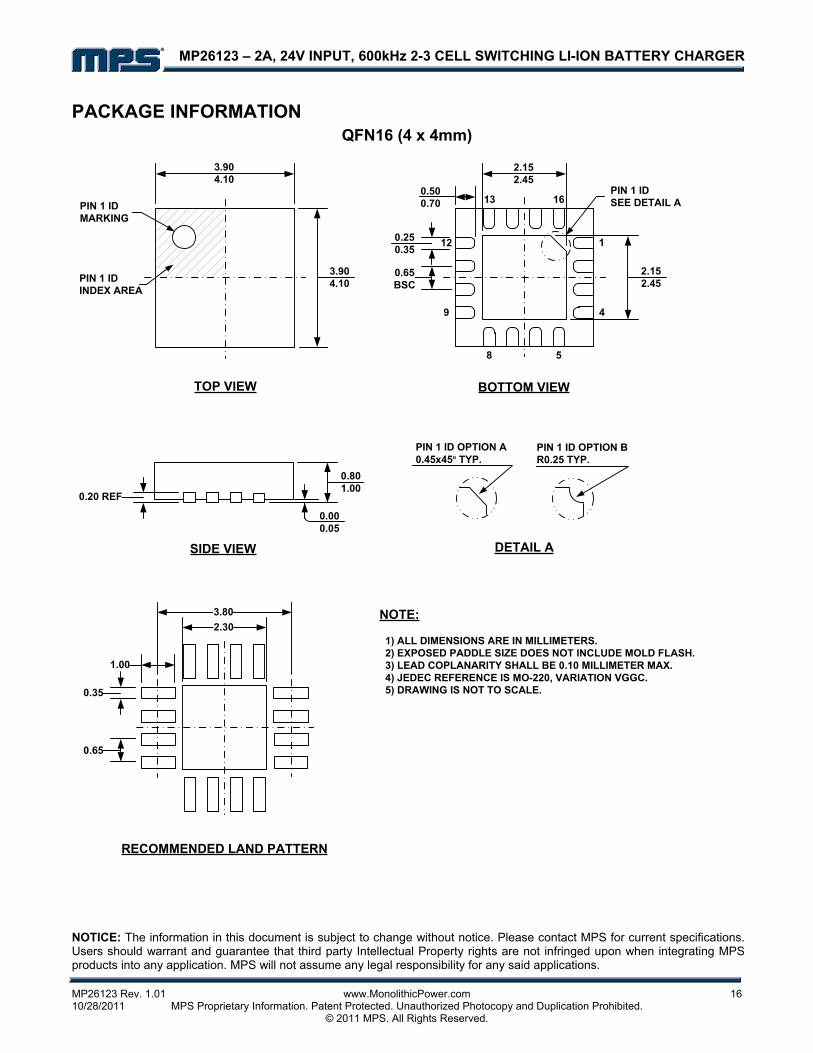
PACKAGE INFORMATION QFN16 (4 x 4mm)
SIDE VIEW
TOP VIEW
1
1613
12
9
8 5
4
BOTTOM VIEW
3.904.10
2.152.45
3.904.10
2.152.45
0.65BSC
0.250.35
0.801.00
0.000.05
0.20 REF
PIN 1 IDMARKING
2.30
0.65
0.35
RECOMMENDED LAND PATTERN
3.80 NOTE:
1) ALL DIMENSIONS ARE IN MILLIMETERS. 2) EXPOSED PADDLE SIZE DOES NOT INCLUDE MOLD FLASH. 3) LEAD COPLANARITY SHALL BE 0.10 MILLIMETER MAX. 4) JEDEC REFERENCE IS MO-220, VARIATION VGGC. 5) DRAWING IS NOT TO SCALE.
PIN 1 IDSEE DETAIL A
PIN 1 ID OPTION A0.45x45º TYP.
PIN 1 ID OPTION BR0.25 TYP.
DETAIL A
PIN 1 IDINDEX AREA
1.00
0.500.70

Mouser Electronics
Authorized Distributor
Click to View Pricing, Inventory, Delivery & Lifecycle Information: Monolithic Power Systems (MPS):
MP26123DR-LF-P MP26123DR-LF-Z