ms thesis of christian birk application and evaluation of
TRANSCRIPT

MS Thesis of Christian Birk
Application and Evaluation of FPAA
Table of contents
1 Introduction 1
2 Elements of filter design 2
3 FPAA technology 4
3.1 Capacitor bank diagram................................................................................................................................... 5
3.2 Switch technology ........................................................................................................................................... 6
4 Analysis of s/c circuits, theory and technique 7
4.1 Basic concept of the s/c technique ................................................................................................................ 7
4.2 Analysis of parasitic insensitive integrators ................................................................................................. 8
4.2.1 Non-inverting integrator ........................................................................................................................................8
4.2.2 Inverting integrator ...............................................................................................................................................10
4.3 Signal flow graph analysis.............................................................................................................................10
5 Sources of error in FPAA operation 13
5.1 Capacitor error model...................................................................................................................................13
5.1.1 Quantization error.................................................................................................................................................13
5.1.2 Macroscopic manufacturing errors.....................................................................................................................14
5.1.3 Microscopic manufacturing errors .....................................................................................................................14
5.2 Additional interconnect capacitances ..........................................................................................................15
5.3 Operational amplifier errors.........................................................................................................................19
5.3.1 Limited bandwidth ................................................................................................................................................19
5.3.2 Finite gain..............................................................................................................................................................19

Table of contents
5.3.3 Finite input and zero output impedance ..............................................................................................................19
6 Errors due to time-discrete filter implementation 21
6.1 Comparison of continuous and s/c biquad filter .........................................................................................21
6.2 Approximation methods for z- to s-domain mapping.................................................................................26
6.2.1 Forward Euler transform......................................................................................................................................27
6.2.2 Backward Euler transform...................................................................................................................................28
6.2.3 Bilinear transform ................................................................................................................................................28
6.3 Calculation of new capacitor size selection rules ......................................................................................29
6.3.1 Low-Q filter implementations.............................................................................................................................30
6.3.2 High-Q filter implementations ............................................................................................................................31
6.4 Low-pass filter realizations ..........................................................................................................................32
6.4.1 Low-pass, low-Q filter .........................................................................................................................................32
6.4.2 Low-pass, high-Q filter ........................................................................................................................................33
6.5 High-pass filter realizations .........................................................................................................................34
6.5.1 High-pass, low-Q filter ........................................................................................................................................35
6.5.2 High-pass, high-Q filter .......................................................................................................................................35
6.6 Band-pass filter realizations .........................................................................................................................36
6.6.1 Band-pass, low-Q filter ........................................................................................................................................36
6.6.2 Band-pass, high-Q filter .......................................................................................................................................37
6.7 Band-stop filter realizations .........................................................................................................................38
6.7.1 Band-stop, low-Q filter ........................................................................................................................................38
6.7.2 Band-stop, high-Q filter .......................................................................................................................................39
6.8 Capacitor size scaling....................................................................................................................................40
7 Filter measurements 41
7.1 Measurement setup........................................................................................................................................41
7.2 Evaluation of the chip performance .............................................................................................................42
7.2.1 Comparison between z-domain analysis and measurements.............................................................................43

Table of contents
7.2.2 Variations among different cells.........................................................................................................................46
7.3 Comparison of capacitor size selection rules.............................................................................................49
7.3.1 Low-pass, low-Q filter measurements................................................................................................................49
7.3.2 Low-pass, high-Q filter measurements...............................................................................................................51
7.3.3 High-pass, low-Q filter measurements...............................................................................................................54
7.3.4 High-pass, high-Q filter measurements..............................................................................................................57
7.3.5 Band-pass, low-Q filter measurements...............................................................................................................60
7.3.6 Band-pass high-Q filter measurements...............................................................................................................63
7.3.7 Band-stop, low-Q filter measurements...............................................................................................................63
7.3.8 Band-stop high-Q filter measurements...............................................................................................................67
8 Analysis of results 68
8.1 Calculation of an overall error bound ..........................................................................................................68
8.2 Definition of error in dB...............................................................................................................................70
8.2.1 Magnitude error in dB..........................................................................................................................................70
8.2.2 Magnitude error bound in dB...............................................................................................................................71
8.3 Error bound graphs ........................................................................................................................................71
8.3.1 Low-Q filter error bound .....................................................................................................................................72
8.3.2 High-Q filter error bound ....................................................................................................................................74
8.4 Comparison of error bounds and measurements ........................................................................................76
8.4.1 Measured error and error bound for low-pass, low-Q filter.............................................................................77
9 Discussion of other filter implementations 81
9.1 Characterisation of s/c circuits ....................................................................................................................81
9.2 Switched current technique...........................................................................................................................81
10 Conclusions and further research 85
11 References 87

Table of contents

1
1 Introduction
This document deals with the design and evaluation of electronic filters implemented on a Field
Programmable Array (FPAA).
Filters occur widely in electronic circuits associated with modern audio, communications, and signal
processing fields. In audio systems, filters are used for pre-amplification, equalization, and tone control.
Communication circuits use them for the tuning of specific frequencies and the elimination of others. In
telephony, filters are used to decode the tone frequencies used for dialing. Digital signal processing
systems incorporate filters to prevent aliasing and to reconstruct the signal. In fact, it is difficult to find
any moderately complex electronic device that does not contain one or more filters.
Variations in filter implementations have evolved drastically over the years as a result of changes in
technology. Originally, electrical filters were realized in the form of RLC circuits. As it is difficult to
have accurate inductors for mass production, the fact that active components of good quality were
developed improved the situation. Especially when operational amplifiers became available in large scale,
they provided a means for eliminating inductors, thus leading to active RC filters. With the introduction
of fully integrated monolithic filters, new techniques like switched capacitors found a very broad range of
applications, as the use of MOS switches and capacitors allowed for eliminating chip-area consuming
resistors on the chip.
Applying the FPAA, filters are set up using switched capacitor (s/c) technology with variable capacitor
sizes to implement a desired filter. As it will be shown, not only the variety of possible circuits that can
be implemented on the chip makes the FPAA so outstanding but also the accuracy of its operation
confirmed by measurements.

2
2 Elements of filter design
Electronic filters comprise a specific class of systems which can be looked at as frequency-selective
signal transmission devices. Signals of certain ranges of frequencies belonging to the pass-bands are
passed from the input to the output, while others in the stop-bands are rejected.
Using a FPAA, numerous applications incorporating filters are possible. Signal conditioning of sensors
may include amplification, linearization and filtering, which all can be done on one FPAA. Apart from
that, filtering in audio-frequency applications, remote sensing, and even adaptive filter implementations
are possible areas were a FPAA can be successfully utilized.
The usual way filters are designed is to have a concrete specification of the transmission characteristics
of the filter. This, of course, does not mean a specification in the form of an ideal characteristic, since
physical circuits are unable to realize idealized characteristics. What we have to specify is bounds for the
deviation of the pass-band transmission from the ideal 0dB and what is allowed to be transmitted in the
stop-band, specified by a minimum attenuation. Apart from that, a transition band is introduced which
extends from the pass-band edge frequency to the stop-band edge frequency in the case of a low-pass
filter. The ratio of these two is a measure for the sharpness of the low-pass filter response. To summarize
the low-pass example, there are four parameters to be set, the pass-band edge frequency, the maximum
allowed variation in pass-band transmission, the stop-band edge frequency, and the minimum required
stop-band attenuation. For high-pass filters the requirements are identical, whereas in the band-pass and
band-stop case there are some more parameters needed.
Once all the specifications are fixed for the respective application, one has to think about how to
transform the filter information into an actual transfer function. This process is called filter
approximation. Usually, this is performed using computer programs. Functions which are frequently used
for the approximation procedure are Butterworth filter functions, Chebyshev filter functions, and Elliptic
or Cauer filter functions. [Huelsman 1993, Van Valkenburg 1982].

2 Elements of filter design 3
As a result of the approximation, we get the transfer function in the s-domain. Its order is dependent on
how tight the specifications are formulated.
The most straightforward way how filters are implemented on the Field Programmable Analog Array is
that we cascade second order filter transfer functions, and, in the case of an odd filter order, one first
order transfer function. As the output impedance of each block is taken at the output terminal of an
operational amplifier where the impedance level is low (ideally zero), the transfer functions of the
individual blocks are not changed by cascading.
Due to the availability of 20 operational amplifier cells, it is possible to realize a filter of 20th order on
one FPAA-chip.
In the following text, we will only concentrate on second order transfer functions, as they are the major
building blocks for higher order filters. If the behavior of the second order transfer function
implementation is known and understood, it is only a very small step to implement filters of higher order.
Then, the main issue is the filter approximation.

4
3 FPAA technology
The FPAA in its current version, the MPAA020, is an “electronic breadboard” that provides an ideal
medium for quickly designing, debugging, and implementing a wide array of analog circuits, which
reduces development cycle times and enables the user to meet market introduction timelines.
The technology for the FPAA is based upon switched capacitor circuit technology. Analog resources in
the MPAA020 are contained in configurable analog blocks (CAB’s) which incorporate a switched
capacitor CMOS operational amplifier, comparator, capacitor banks, CMOS switches and SRAM. The
function of each cell may be programmed to connect with any of the other cells in the array. Data stored
in SRAM control the switches that program various capacitance values, for both static and dynamic
capacitors, in the input and feedback signal paths of the operational amplifier. Analog functions such as
programmable gain stages, adders, subtractors, rectifiers, sample & hold circuits, and first order filters
can be implemented in a single cell (CAB). Higher level functions such as biquad filters, which are
subject of this study, PLL’s, level detectors, and others can be implemented using two or more cells.
The MPAA020 contains 41 operational amplifiers, 100 programmable capacitors, and 6864 switches. The
switches control circuit connectivity, capacitor values, and other selectable features. The array is
structured in a grid that contains 20 CAB’s arranged in a 4 5¥ matrix. The programmable CAB’s rely on
the configuration logic on the chip to control the connectivity within the array and functionality in each
CAB. An 8-bit programmable band-gap voltage reference is available to each cell. Configuring an analog
design within the array is performed by downloading 6K bits of data via RS232 communications from a
PC or EPROM. The data stream contains information to configure the individual cells, the cell to cell
interconnections, internal voltage reference as well as the input and output connections. During the
configuration download process, all cells are placed in a power-down mode, which is exactly what is done
with individual cells not in use by the actual design in order to minimize the power dissipation. [Motorola
1997b, Motorola 1997c, Motorola 1997d].

3 FPAA technology 5
3.1 Capacitor bank diagram
Generally, in s/c circuits unit capacitors within one capacitor bank are connected together in parallel to
obtain the desired capacitor value. The number of possible capacitor values is only limited by the bank
size if a binary configuration is used, which is shown in the following diagram:
Figure 3-1. Schematic of capacitor bank organization.
In Figure 3-1, the squares represent unit capacitors of size u. Their number defines the maximum size of a
capacitor that can be implemented using a single bank. The bank capacitors are arranged in groups of unit
capacitors as shown in Figure 3-1, so that these unit capacitors add up. Such connected capacitors are
called sub-arrays, and these sub-arrays are organized in binary fashion, so one capacitor bank consists of
sub-arrays with capacitor values 1u, 2u, 4u, 8u, 16u, 32u, ... .
In the case of the MPAA020, all capacitor banks consist of 256 unit capacitors, which means that the
largest sub-array is composed of 128u. Altogether, we can realize all integer capacitor sizes between 1u
and 255u. One unit capacitor, in the above diagram the first one, is not used and therefore has only dummy
function. The reason why it has been implemented is to maintain the square symmetry of the whole
capacitor bank layout.
1 2 4 8
16
128
32

3 FPAA technology 6
The fact that we can only realize integer capacitor values will be accounted for in a following section, as
quantization effects significantly contribute to the circuit performance. Wherever the design allows for,
we try to parallel two capacitor banks within on cell to double the maximum capacitor value.
A more detailed description of the capacitor bank including a capacitor error model is presented in
[Palusinski et al. 1997b].
3.2 Switch technology
Dynamic and static switches on the FPAA are implemented in CMOS technology. Not only does a CMOS
transmission gate offer extremely low power consumption, but also effects caused by clock feed-through
can be eliminated or minimized by proper design. Apart from that, CMOS has a wider valid input signal
range than for example a single NMOS switch.
Vdd
Vss
Signal In Signal OutF
F
Figure 3-2. CMOS transmission gate used as a switch.
In the text to follow, wherever a CMOS transmission gate according to Figure 3-2 is employed, we will
simply draw a switch symbol for the sake of drawing simplicity. However, for practical implementations
the actual realization should always be kept in mind.

7
4 Analysis of s/c circuits, theory and technique
Switched capacitor circuits operate as time-discrete signal processors without the use of A/D or D/A
converters. As a result, these circuits are most easily analyzed with the use of z-transform techniques.
Typically, anti-aliasing and smoothing or reconstruction filters are required.
Especially for filtering, switched capacitor circuits have become extremely popular due to their accurate
frequency response as well as good linearity and dynamic range. Accurate discrete-time frequency
responses are obtained since filter coefficients are determined by capacitor ratios which can be set quite
precisely in an integrated circuit (in the order of 0.1 percent). Such an accuracy is orders of magnitude
better than that which occurs for integrated RC time constants (which can vary by as much as 20 percent).
Once the coefficients of a switched capacitor discrete-time filter are accurately determined, the overall
frequency response remains a function of the clock frequency. Fortunately, using crystal oscillators,
clock frequencies can be set very precisely. [Johns and Martin 1997].
4.1 Basic concept of the s/c technique
The switched capacitor technique is based on the realization that a capacitor switched periodically
between two circuit nodes is equivalent to a resistor connecting these nodes if we are interested in an
average value of current over a period of time exceeding a number of times the switching period.
A circuit diagram for this basic s/c circuit is shown in Figure 4-1:
vin vout1 2
C
Figure 4-1. Basic s/c circuit replacing a resistor for high switching frequencies.
During the time when the switch is in position 1, the capacitor is charged to the voltage applied to the
input, v in . So the total charge on the capacitor C is Q C v in1 = in steady state. When the switch changes to

4 Analysis of s/c circuits, theory and technique 8
position 2, the new charge on the capacitor for the steady state will be Q C vout2 = . The net charge
transferred from the input to the output during one switching period is then
DQ Q Q C v vin out= - = -1 2 ( ) . (4-1)
This is equivalent to a current i flowing from the input to the output,
iQ
T
C v v
Tin out= =
-D ( ), (4-2)
and from this equation we can easily calculate an equivalent resistor value
RT
C= . (4-3)
It can be seen that in order to determine the resistance value both, the clock period and the capacitance,
have to have specific values.
4.2 Analysis of parasitic insensitive integrators
4.2.1 Non-inverting integrator
+
_
C2
vout
Φ 2
Φ 1
C1
vin
Φ 1
Φ 2
Figure 4-2. A realization of a non-inverting integrator using s/c circuit simulating a negative
resistor.
The output voltage vout is only valid during clock phase F1 when F1 is high and appropriate switches are
closed.
Figure 4-2 as well as all of the following s/c circuits make use of both clock phases, F1 and F2 , which
are defined according to the following clocking scheme (Figure 4-3):

4 Analysis of s/c circuits, theory and technique 9
Φ1, Φ2
t
T
von
voff
n-3/2 n-1 n-1/2 n n+1/2 n+1
Φ2 Φ1 Φ2 Φ2Φ1 Φ1
Figure 4-3: Two phase non-overlapping clocking scheme used in s/c circuits.
To analyze the circuit in Figure 4-2, the charge behavior has to investigated. Obviously, a virtual ground
appears at the operational amplifier’s negative input. Assuming an initial integrator output voltage of
v nT Tout ( )- , then the charge on C2 is equal to C v nT Tout2 ( )- at time ( )nT T- . At that time, F1 is just
turning off (F2 is off), so the input signal v in is sampled, leading to a charge on C1 being equal to
C v nT Tin1 ( )- . When F2 goes high, C1 is forced to discharge as it is connected to ground with the left
plate and to virtual ground with the right plate. The discharging current flows through C2 , so the charge on
C1 is added to C2 .
A positive input voltage will result in a positive voltage across C2 and therefore a positive output voltage.
At the end of F2 we obtain the charge equation
C v nT T C v nT T C v nT Tout out in2 2 12( / ) ( ) ( )- = - + - . (4-4)
The charge on C2 at time ( )nT at the end of the next F
1 is equal to that at time ( / )nT T- 2 , so we can
write
C v nT C v nT T C v nT Tout out in2 2 1( ) ( ) ( )= - + - . (4-5)
Dividing equation (4-5) by C2 and applying the z-transform yields
V z z V zC
Cz V zout out in( ) ( ) ( )= +- -1 1
2
1 .(4-6)
Therefore, the transfer function can be expressed as
H zV z
V z
C
C
z
zout
in
( )( )
( )= =
-
-
-1
2
1
11 ,
(4-7)

4 Analysis of s/c circuits, theory and technique 10
which comprises a non-inverting discrete-time integrator with a delay of a full clock period from input to
output (represented by the z -1 in the numerator). Or, in other words, equation (4-7) states the Forward
Euler z-transform of a non-inverting continuous-time lossless integrator.
4.2.2 Inverting integrator
+
_
C2
vout
Φ 1
Φ 2
C1Φ 1
Φ 2
vin
Figure 4-4. A realization of an inverting integrator using s/c circuit simulating a positive resistor.
As can be seen from comparison of Figure 4-2 and Figure 4-4, the only difference between these two
circuit diagrams is that two switches with their respective on-phases are exchanged.
Using similar arguments as before, the above circuit (Figure 4-4) can be analyzed which yields the charge
equation
C v nT C v nT T C v nTout out in2 2 1( ) ( ) ( )= - - . (4-8)
Analogously dividing by C2 and taking the z-transform, we get
H zv z
v z
C
C zout
in
( )( )
( )= = -
- -1
2
1
1
1 , (4-9)
which is the transfer function for a delay-free inverting discrete-time integrator or, to be more precise,
the Backward Euler z-transform of an inverting integrator.
4.3 Signal flow graph analysis
It would be quite tedious to perform charge analysis on larger circuits, therefore simpler, more general
analysis rules can be set up on the basis of the discussion of non-inverting and inverting integrators.
Consider the integrator with multiple inputs shown in Figure 4-5.

4 Analysis of s/c circuits, theory and technique 11
+
_
CA
Vout(z)
Φ2C2
Φ1
Φ1
Φ2
C1
V1(z)
V2(z)
Φ1C3
Φ2
Φ1
Φ2
V3(z)
Figure 4-5. Integrator with different input circuits.
Using the principle of superposition, we can analyze the circuit in Figure 4-5 by looking at one input only
and setting the other two inputs to zero. Therefore, the following transfer functions are obtained:
H zV z
V z
C
Cout
A
1
1
1( )( )
( )= = - , (4-10)
H zV z
V z
C
C
z
zout
A
2
2
21
11( )
( )
( )= =
-
-
- ,(4-11)
H zV z
V z
C
C zout
A
3
3
3
1
1
1( )
( )
( )= = -
- - . (4-12)
Summation of (4-10), (4-11), and (4-12) yields the overall transfer function of the circuit in Figure 4-5.
Now, if the operational amplifier stage is expressed as -- -
1 1
1 1C zA
, the formulas for the three input
circuits can be calculated using the transfer functions for each branch.
From H z1 ( ) we get a transfer function of C z1
11( )- - for the non-switched capacitor input, H z2 ( ) yields
- -C z2
1 for the non-inverting input, and from H z3 ( ) the transfer function of the inverting input is simply
C3 .
These results are summarized in the following signal flow graph, Figure 4-6:

4 Analysis of s/c circuits, theory and technique 12
V1(z)
V2(z)
V3(z)
Vout(z)
C 1(1-z-1)
-C2 z-1
C 3
-- -
1 1
1 1C zA
Figure 4-6. Signal flow graph for integrator with different input stages.
It has to be mentioned that all biquad filters can be analyzed using the above derived rules for the different
building blocks. The direction of the signal arrows can be determined by the assumption that the signal
branches have as input signals the operational amplifier output voltages and as output signals the
operational amplifier input currents.
Table 4-1 shows a summary of the derived representations of s/c circuit elements which occur in s/c
biquad circuits:
unswitched capacitorC
C z( )1 1- -
negative resistor
Φ2C
Φ1
Φ1
Φ2- -C z 1
positive resistor
Φ1C
Φ2
Φ1
Φ2C
integrator+
_
C
-- -
1 1
1 1C z
Table 4-1. Basic s/c building blocks.
See [Moschytz 1984] and [Johns and Martin 1997].

13
5 Sources of error in FPAA operation
5.1 Capacitor error model
The existing error model is stated in [Palusinski et al. 1997a] and explained in more detail in [Palusinski
et al. 1997b]. Therefore, a very comprehensive description is not given here, but the resulting relative
error bound equation is stated and its components are explained in detail.
The capacitor error is defined as follows: Cl is the ideal capacitor of size l times the unit capacitance u,
whereas C l is the real capacitor value containing an error. Therefore, the relationship between C l and C l
introducing a relative error, a( )C l , can be written as:
C C Cl l l= +1 a( ) . (5-1)
The relative error bound d ( )C l of the relative error a( )C l is expressed as
ds e
l( )( )
( )Cl
ql u
ll = + +1
2
1 , (5-2)
where 1
2l represents the quantization error, q
l u
1 s e( ) the microscopic manufacturing error and l( )l the
error due to macroscopic manufacturing errors.
5.1.1 Quantization error
The first component in the equation for the capacitor error bound is the quantization error. According to
chapter 3.1, on one capacitor bank we can implement integer multiples of the unit capacitor size u,
expressed as lu with l in the range from 1 to 255. As it is very probable that a non-integer multiple of u is
needed, we have to quantize its value to the nearest integer l in its respective range. Since we can at most
require a capacitance halfway between lu and (l+1)u, we can account for this error with the value of the
worst case. So the relative error bound
d Ql
=1
2(5-3)
accounting for quantization effects is obtained.

5 Sources of error in FPAA operation 14
5.1.2 Macroscopic manufacturing errors
Chip manufacturing errors can be divided into two categories, which are the macroscopic and the
microscopic errors. Macroscopic errors effect all capacitor banks on the chip with negligible variations,
as they have a larger extent. They can even effect all of the chips on a wafer. Possible sources are edge
effects on the perimeter of wafers and gradients in the oxide thickness developed during fabrication. We
try to take this macroscopic errors into account by adding a bias value to the model for the relative error
bound,
d lM l= ( ) . (5-4)
Although we do not know exactly yet in what way the bias l really depends on the selected capacitor size,
the notation l( )l expresses that influence on the bias error could be significant in some way. However,
this is not exploited yet, and more measurements and statistical analysis would be needed.
5.1.3 Microscopic manufacturing errors
Microscopic errors are the error contributions inside a single capacitor bank of unit capacitors. This error
is comprised of random variations between capacitors, like varying oxide thickness, size and shape of the
unit capacitors caused by the plate formation and etching process. Unfortunately, we can account for this
error only by a statistical statement. e is the microscopic error of a unit capacitor and is assumed to be
an independent zero-mean random variable with normal probability distribution, and s e( ) is its standard
deviation. Summing up l times the e in the standard deviation for a capacitor of size Cl=lu yields the
standard deviation of a new random variable z and can be expressed as s s e( ) ( )z l= ◊ . Then a tolerance
level q zs ( ) is chosen, where q=3 defines “6-sigma” quality requirements. So the error contribution
becomes q l us e( ) / , and for the relative error we get
ds e
m = ql u
1 ( ) . (5-5)

5 Sources of error in FPAA operation 15
If we now assume that the macroscopic an microscopic error components are additive and independent,
we obtain the relative error bound expression by adding all relative error components,
d d d d m( )C l Q M= + + , resulting in equation (5-2).
5.2 Additional interconnect capacitances
Apart from the capacitor error model described above, there are more error sources which are caused by
the capacitor layout. Within one capacitor bank and for capacitor bank interconnections, stray capacitors
effect the accuracy of the wanted capacitor size. We will refer to them as additional interconnect
capacitances. Although the effort to compensate those capacitor errors is huge, they cannot be eliminated
totally. Detailed observations of the actual chip behavior and theory developed from the layout diagram
still confirm the existence of errors due to interconnect capacitances.
In the following, we investigate bank interconnection capacitance caused by overlap of the bottom layer
and the metal layer.
bottom plate
top plate
metal layer
metal layer/top plateinterconnection
Figure 5-1: Simplified part of the capacitor bank layout
Figure 5-1 shows a simplified part of the capacitor bank layout, representing a sub-array consisting of two
unit capacitors. We see that the bottom plate of a single unit capacitor is larger than its top plate. To

5 Sources of error in FPAA operation 16
connect a single capacitor either with the other capacitors within a sub-array or to connect two sub-arrays,
metal connections (hatched area) are needed. These interconnections link the respective top plates.
By inspection of Figure 5-1 it can be seen that each sub-array has a specific area of overlap of the metal
layer and the bottom plate (gray-hatched area). These regions of overlap occur either due to
interconnections within the sub-array or due to the connection of different sub-arrays. Therefore,
depending on the capacitor size to be realized in one bank, the additional interconnection capacitor area
will increase or decrease.
At this point it is important to mention that the performance of a s/c circuit is not dependent on a single
capacitor value but on the ratio of two capacitors. Therefore, the main goal is to keep the tracking error
(i.e. the error in the ratio) as small as possible. If we now try and design the capacitor bank to get an
additional interconnect capacitance exactly proportional to each possible capacitor size, the tracking
error will disappear.
To obtain an adequate representation, a new approach to describe the implemented capacitor of size l is
chosen:
C a C a Clk
k
M
k
k
Mlk k
[ ] [ ] [ ] [ ]= + += =
 Â2
0
2
0
D c , a k Π0 1,k p (5-6)
where M equals 7 for a capacitor bank size of 255. a k stands for the binary digits in the digital capacitor
size representation of l, Ck[ ]2 is the ideal capacitance containing 2 k unit capacitors, and DC
k[ ]2 is the error
term due to the aforementioned error sources plus the sub-array internal interconnections. c [ ]l finally
represents the interconnection capacitance between different sub-arrays.
Therefore, the ideal capacitor of size l u◊ can be expressed as
C a C a ulk
k
kk
k
k[ ] [ ]= =LNMM
OQPP= =
 Â2
0
7
0
7
2 . (5-7)
The sub-array internal interconnect capacitance x [ ]l of a capacitor incorporating l unit capacitors can be
written in analogy to (5-7) as

5 Sources of error in FPAA operation 17
x x a[ ] [ ] ( )lk
k
k k
k
a a b uk
= == =
 Â2
0
7
0
7
. (5-8)
The bk whose numerical values are shown in Table 5-1 represent numbers in proportion to the additional
capacitor area obtained by measuring the area size in the capacitor bank layout. A scaling factor a has to
be introduced, so that x [ ]l represents a capacitance. Its numerical value has to be determined by capacitor
error measurements, which has not been done yet.
b7 b6 b5 b4 b3 b2 b1 b0
255.3 124 62 31 16.3 7.3 3.3 1
Table 5-1. Numerical values for bk obtained by capacitor bank layout analysis.
For the interconnection capacitances c [ ]l between different sub-arrays, we get equation (5-9) from
analysis of the layout.
ca
[ ];
;
l k
k
u a a
otherwise
=◊ >
RS|T|
=Â2 0
0
4
0
3
, (5-9)
where again the scaling factor a from above is used.
Applying the above equations for each possible capacitor size to be set up with in bank, a graph (Figure 5-
2) can be plotted showing the results for the different capacitor sizes. It is important to mention that the
scaling factor a from the above equations (5-8) and (5-9) was chosen to be 1 as statistical capacitor error
measurements were not yet available. This has no influence on the general shape of the curves.

5 Sources of error in FPAA operation 18
Title: ic_cap.epsCreator: MATLAB, The Mathworks, Inc.CreationDate: 02/24/98 14:31:36
Figure 5-2. Additional interconnection capacitance and its linearity error.
Looking at the upper half of Figure 5-2, one could suppose that the curve is linear. If there were no error,
we would in fact get an ideal curve of linear shape. But as can be easily seen from the computation of the
relative linearity error in the lower half of Figure 5-3, there are discontinuities at certain capacitor sizes
in the plot. Especially at small capacitor values, these discontinuities introduce a strong non-linearity in
the graph (it “wobbles”). Speaking in terms of the tracking error, it is obvious that using small capacitors
in the s/c circuit decreases the accuracy of the desired capacitor ratio due to the interconnection capacity.
This leads to a deterioration of the overall circuit performance. [Anderson et al. 1998].
5 Sources of error in FPAA operation 19
5.3 Operational amplifier errors
5.3.1 Limited bandwidth
The operational amplifiers used as core amplifiers in each cell are designed in such a way that there is no
deterioration of FPAA signals due to the maximum bandwidth of the amplifier. The maximum clocking
frequency of the MPAA020 is 1MHz, thus the allowable input signal frequency range is limited to
500kHz by the sampling theorem. Now, the core amplifiers are designed to have a bandwidth of more than
one order of magnitude higher than the highest valid input frequency. Therefore, we can neglect the error
caused by bandwidth limitations of the core amplifiers.
5.3.2 Finite gain
The open loop gain of the core amplifiers is higher than 90dB, which in practical terms is quite close to
the ideal operational amplifier with infinite gain. So in comparison with other error sources the deviation
due to the finite but very high open loop gain is negligible.
5.3.3 Finite input and zero output impedance
The core amplifiers are required to have infinite input impedance and zero output impedance. This is very
important for the behavior of higher order filters which are composed of second and first order building
blocks in cascade. Again, due to the extremely well designed core amplifiers, we can neglect any
influence of cascading on the behavior of signals. The largest potential source of error, which may be due
to the connections through input and output pins on the chip is reduced by providing unity gain buffers to
all input and output pins. So, for example, if a current is drawn due to a load at the output, this does not
influence the internal signal at all as the current required is provided by the buffer amplifier. Therefore,
we can assume ideal behavior of core amplifiers also in this case.
5 Sources of error in FPAA operation 20
In general, it is not necessary to include operational amplifier errors (also those ones not mentioned here
like slew rate, CMRR, etc.) in the present analysis as capacitor effects dominate the error behavior of the
MPAA020.

21
6 Errors due to time-discrete filter implementation
6.1 Comparison of continuous and s/c biquad filter
The general second order filter transfer function (also called biquad) is usually expressed in the form
H sK s K s K
sQ
sbiquad ( ) = -
+ +
+ +2
2
1 0
2 00
2ww
,(6-1)
where the parameters K0, K1, K2, w 0 , and Q specify the filtering behavior. [Sedra, Smith 1991].
An active-RC realization of a low-Q biquad filter is shown in Figure 6-1:
+
_
+
_+
_
OP2
RR
OP1
R2 R4
CB
OP3
CA
C1"
R1'
R1
Vin
Vout
R3
Figure 6-1. Active RC-realization of low-Q biquad filter.
The operational amplifier block in Figure 6-1 consisting of OP2 and the two identical resistors R in the
middle of the schematic functions as a unity gain signal inverter, so for the construction of a s/c version
of the circuit, the resistor R3 can be interpreted as a negative resistor. Using KVL and KCL to analyze the
remaining circuit, the ideal transfer function in the s-domain for the low-Q biquad circuit is
H s
C C sC
Rs
R R
C C sC
Rs
R R
ideal low Q
AA
A BA
( )
"
'
= -+ +
+ +
1
2
1 1 3
2
4 2 3
1
1 .
(6-2)

6 Errors due to time-discrete filter implementation 22
Now, if all resistors are replaced by their ideal switched capacitor equivalents, which means that the
resistor values are substituted by RT
C= (holding for very high clock frequencies), we get the following
expression:
H s
C s CT
sC C
C T
C s CT
sC C
C T
cont low QA
B
A
( )
" '
=+ +
+ +
1
2
11 3
2
24
2 32
1 1
1 1.
(6-3)
This is an approximate transfer function, valid only for rough calculations, as the error introduced by the
assumption of an infinite clock frequency increases with increasing signal frequencies.
In the actual circuit implementation, instead of replacing the resistors in Figure 6-1 by the stray sensitive
basic s/c circuit in Figure 3-1, the s/c building blocks from Table 4-1 are used, as these circuits not only
offer insensitivity against stray capacitances but also positive and negative equivalent resistor.
The following schematic given in Figure 6-2 is identical to the circuit of Figure 6-1 with the resistors
simply replaced by their s/c equivalents.
C1"
+
_
CA
Vin
+
_
CB
Vout
Φ2 Φ2
Φ1
C1
Φ1
Φ2 Φ2
Φ1
C1'
Φ 1
Φ1 Φ2
Φ 2
C3
Φ1
Φ2 Φ2
Φ1
C4
Φ1
Φ2 Φ2
Φ1
C2
Φ1
Figure 6-2. Implementation of low-Q biquad filter circuit in s/c technology.

6 Errors due to time-discrete filter implementation 23
To perform exact analysis, it is convenient to transform the original s/c circuit (Figure 6-2) into a signal
flow chart. To do so, we use the rules stated in chapter 4.3, which yield the representation shown in Figure
6-3:
-- -
1 1
1 1C zA
-- -
1 1
1 1C zB
C1
C z1
11" ( )- -
C 2
++Vin Vout
C1
'
- -C z3
1
C 4
Figure 6-3. Signal flow chart representation of the s/c circuit implementing a low-Q biquad.
Analysis of this circuit in the z-domain yields the transfer function
H zC C C z C C C C C C z C C
C C C z C C C C C C z C Cs c lowQ
A A A A
B A A A B A B
/( )
( ) ( )
( ) ( )
' " ' " "
= -+ + - - ++ + - - +
1 1 1 1 1
2
1 3
4
2
2 3 4
2
2 .
(6-4)
At this point it is important to mention that the actual s/c implementation of the above filter circuit looks
slightly different. Careful examination of the circuit in Figure 6-2 reveals that some of the switches are
redundant. Using the technique called switch sharing, circuit designers implement the s/c filter in the
fashion presented in Figure 6-4, without any degradation of performance.

6 Errors due to time-discrete filter implementation 24
C1"
+
_
CA
Vin
+
_
CB
Vout
C4
C2
Φ 2C1
Φ 1
Φ 2
Φ 1
C1'
Φ 2C3
Φ 1
Φ 1
Φ 2
Φ 2
Φ 1
Figure 6-4. Switch sharing applied to the s/c circuit of a low-Q biquad.
As mentioned before, the discussed implementation yields low-Q filters. The same derivation is now done
for a high-Q biquad filter, which can be realized in active-RC fashion as shown in Figure 6-5.
+
_
+
_+
_
OP2
RR
OP1
R2
CB
OP3
CA
C1"
R1
Vin
Vout
R3
C4C1'
Figure 6-5. Active RC-realization of high-Q biquad filter.
Analysis of the circuit in Figure 6-5 yields the s-domain transfer function of this high-Q biquad
implementation:
H s
C C sC
Rs
R R
C C sC
Rs
R R
ideal high Q
A
A B
( )
"'
= -+ +
+ +
1
2 1
3 1 3
2 4
3 2 3
1
1 ,
(6-5)

6 Errors due to time-discrete filter implementation 25
Replacing the resistor values R R R1 2 3, , by their equivalent capacitor values, we obtain the equation
H sC C s C C
Ts C C
T
C C s C CT
s C CT
cont high Q
A
A B
( )
" '
= -+ +
+ +
1
2
1 3 1 3 2
23 4 2 3 2
1 1
1 1 . (6-6)
Analogously, we exchange all resistor symbols in the above circuit diagram by their s/c equivalents.
Applying the aforementioned switch sharing technique, we get the actual s/c circuit implementation of the
high-Q biquad shown in Figure 6-6.
C1"
+
_
CA
+
_
CB
Vout
Φ 2
Φ 1
Φ 1 Φ 2
Φ 2
C3
Φ 1
C4
C2
Φ 2
Φ 1
C1
C1'
Vin
Φ 2
Φ 1
Figure 6-6. Implementation of s/c circuit for high-Q biquad using switch sharing.
Now, we again apply the time discrete analysis in the z-domain by transforming the s/c circuit diagram
into a signal flow chart. The different circuit components are substituted by their proper z-domain
equations, which yields the diagram shown in Figure 6-7.
-- -
1 1
1 1C zA
-- -
1 1
1 1C zB
C z1
11' ( )- -
C 1
C z1
11" ( )- -
C z4
11( )- -
C 2
++Vin Vo u t
- -C z3
1
Figure 6-7. Signal flow chart of s/c high-Q biquad circuit.

6 Errors due to time-discrete filter implementation 26
The z-domain transfer function of the high-Q biquad is
H zC C z C C C C C C z C C C C
C C z C C C C C C z C C C Cs c highQ
A A A
A B A B A B
/( )
( )
( )
" ' " " '
= -+ + - + -+ + - + -
1 1 1 1 1 3
3 4
2
1 3 3
2
2 3 3 4
2
2. (6-7)
A valuable reference for this section is [Gregorian and Temes 1986], where the above transfer functions
are confirmed.
6.2 Approximation methods for z- to s-domain mapping
The capacitor size selection rules implemented for filter design in the EasyAnalogTM software are based
on continuous s/c circuit analysis. However, as is explained before, this analysis does not yield very
accurate solutions. In order to obtain a s/c filter circuit which is as close as possible to the desired
theoretical transfer function, new capacitor size selection rules based on z-domain analysis should be
derived.
To do so, the z-domain equations of the s/c biquad circuits in Figure 6-2 and Figure 6-6 have to be
transformed into s-domain representations and then comparison with the ideal filters may be used to
develop capacitor size selection rules. It is worth mentioning that the capacitor sizes cannot be
completely determined by such comparison, and thus additional assumptions will have to be made.
A very important step influencing the accuracy of the results is the transition of the filter transfer
function from the z-domain into the s-domain.
For the highest possible accuracy, this transform is accomplished by setting z e sT= [Kammeyer and
Kroschel 1996]. If we expand the exponential function into a Taylor series [Bronstein and Semendjajew
1991], zsT sT sT sT
n
n
= + + + + + +11 2 3
2 3
!
( )
!
( )
!. . .
( )
!. . . , it is obvious that replacing all the z in a transfer
function yields to polynomials of infinite order in the numerator as well as in the denominator.
Now if we want to keep the error between the desired theoretical biquad transfer function and the
implemented transfer function as small as possible, the difference between these two has to be minimized

6 Errors due to time-discrete filter implementation 27
(and, to further improve the filter performance, weighting of the variable s with an appropriate weight
function could be performed).
Unfortunately, analytical minimization of the error leads to a highly nonlinear system of equations, such
that this approach is not practical.
Therefore a compromise is needed, which means that precision is traded for an ease of solution.
6.2.1 Forward Euler transform
The easiest way to obtain an approximation function for the transition from a time-discrete to a time
continuous transfer function is to compare continuous integration with a numerical approach (in steps).
The transfer function of an ideal integrator is represented in the s-domain by G sY s
X s s( )
( )
( )= =
1. Numerical
integration algorithms can be expressed by difference equations, the so called Forward Euler integration
method is recursively written as y nT y nT T T x nT T( ) ( ) ( )= - + - . Simple transformation into the z-
domain yields Y z z Y z T z X z( ) ( ) ( )= +- -1 1 , and by rearranging this expression the Forward Euler transfer
function can be derived, and we get G zY z
X z
T z
z( )
( )
( )= =
-
-
-
1
11 . Comparison of the two integrators yields the
expression z sT= +1 , which in general can be used to transform a z-domain transfer function into a s-
domain transfer function by substitution.
It has to be mentioned that Forward Euler is only conditionally stable, i.e. stability is guaranteed only for
sufficiently small T . The two other methods are considered unconditionally stable.
The Forward Euler approximation is used in most of the available literature about switched capacitors for
the transition from the z- to the s-domain. Theoretical capacitor size selection rules for this
approximation exist [Palusinski et al. 1997a], but the practical filter performance using the rules has not
yet been evaluated.

6 Errors due to time-discrete filter implementation 28
6.2.2 Backward Euler transform
Similar to the Forward Euler method, the Backward Euler method can be expressed in difference equation
form as y nT y nT T T x nT( ) ( ) ( )= - + . Transforming this into the z-domain and rearranging the terms, the
transfer function G zY z
X z
T
z( )
( )
( )= =
- -1 1 is obtained, leading to the approximation formula z sT- = -1 1 .
The error caused by the Backward Euler transform has exactly the same magnitude as the error of Forward
Euler, the only difference lies in the inverted phase sign and absolute stability.
6.2.3 Bilinear transform
A more sophisticated approximation method is the bilinear transform, also known as trapezoidal rule with
the difference equation
y nT y nT T Tx nT x nT T
( ) ( )( ) ( )
= - ++ -
2 . (6-8)
Applying the z-domain transform to this equation we get Y z z Y z TX z z X z
( ) ( )( ) ( )
= ++-
-1
1
2. The transfer
function then can be written as G zY z
X z
T z
z( )
( )
( )= = +
-
-
-2
1
1
1
1, so again comparison with the ideal integrator
leads to
zsT
sT- =
-+
1 2
2 . (6-9)
The impact of these three different approximation rules on the resulting filter is shown in Figure 6-8,
which compares the plots of the magnitude of the frequency response H, and the relative errors defined as
e rel
approx ideal
ideal
H H
H=
- . (6-10)

6 Errors due to time-discrete filter implementation 29
Title: bilfe.epsCreator: MATLAB, The Mathworks, Inc.CreationDate: 03/03/98 13:45:23
Figure 6-8. Effects on transfer function using different mapping approximations
Applying one of the mentioned first order approximations to a time discrete filter transfer function, it is
obvious that the filter order is not changed by the transition into a continuous function as it would be the
case for higher order approximation functions. This makes the derivation of new capacitor size selection
rules straightforward [Birk 1998].
6.3 Calculation of new capacitor size selection rules
According to the equations (6-4) and (6-7), which define the transfer functions for the two described s/c
circuits for low-Q and high-Q filter implementations, the transfer function of the s/c biquad
implementation in the z-domain can be written in general as
H za z a z a
b z b z bs c/ ( ) = -
+ ++ +
22
1 0
22
1 0
. (6-11)

6 Errors due to time-discrete filter implementation 30
Substituting the bilinear approximation formula for z- to s-domain mapping, equation (6-9), into equation
(6-11), the general s-domain equivalent for biquad transfer functions is obtained:
H sa a a s T a a sT a a a
b b b s T b b sT b b bs c/ ( )
( ) ( ) ( )
( ) ( ) ( )= -
- + + - + + +- + + - + + +
2 1 02 2
2 0 2 1 0
2 1 02 2
2 0 2 1 0
4 4
4 4 . (6-12)
Subsequent derivations are split into two parts according to the low-Q and high-Q implementations of
biquads.
6.3.1 Low-Q filter implementations
For the low-Q circuit implementation, the parameters a0, a1, a2 and b0, b1, b2 in equation (6-11) are
defined by the s/c low-Q transfer function (6-4). Comparison between these two equation yields the
numerator and denominator coefficients as functions of capacitor values:
a C C A0 1= " a C C C C C CA A1 1 3 1 1
2= - -' " a C C C A2 1 1= +( )' "
b C CA B0 = b C C C C C CA A B1 2 3 4 2= - - b C C CB A2 4= +( )
Inserting these coefficients into the general s-domain representation of the s/c circuit function, Hs/c(s),
which is stated in equation (6-12), the transfer function in the s-domain for the s/c low-Q biquad circuit
with bilinear approximation can be written in the form:
H sC C C C C C s T C C sT C C
C C C C C C s T C C sT C Cs c low Q
A A A
A A B A
/
' " '
( )( )
( )= -
+ - + ++ - + +
2 4 4 4
2 4 4 41 1 1 3
2 21 1 3
4 2 32 2
4 2 3
. (6-13)
Comparison of equation (6-13) with the desired biquad filter transfer function,
H sK s K s K
sQ
sbiquad ( ) = -
+ +
+ +2
2
1 0
2 00
2ww
(6-1) yields the necessary values for the parameters of low-Q filters
dependent as functions of the capacitor values.
KC C C C C C
C C C C C CA A
A A B
21 1 1 3
4 2 3
2 4
2 4=
+ -+ -
' "
(6-14) K TC C
C C C C C CA
A A B
11
4 2 3
4
2 4=
+ -
' (6-15)
K TC C
C C C C C CA A B
02 1 3
4 2 3
4
2 4=
+ -(6-16) w
0
2 3
4 2 3
22 4
TC C
C C C C C CA A B
=+ -
(6-17)
QC C C C C C C C
C C
A A B
A
=+ -2 3 4 2 3
4
2 4
2
( ) . (6-18)

6 Errors due to time-discrete filter implementation 31
6.3.2 High-Q filter implementations
For high-Q biquad filters, we can proceed analogously to the low-Q case. The coefficients in equation (6-
11) are obtained from equation (6-7) and result in
a C C C CA0 1 1 3= -" ' a C C C C C C A1 1 3 1 3 1
2= + -' " a C C A2 1= "
b C C C CA B0 3 4= - b C C C C C CA B1 2 3 3 4 2= + - b C CA B2 = .
Substituting the values a0, a1, a2, b0, b1, and b2 in equation (6-12), we obtain the s-domain transfer
function
H sC C C C C C s T C C sT C C
C C C C C C s T C C sT C Cs chighQ
A
A B
/
" ' '
( )( )
( )= -
- - + +- - + +
4 2 4 4
4 2 4 41 1 3 1 3
2 21 3 1 3
3 4 2 32 2
3 4 2 3
, (6-19)
and comparison with the theoretical biquad transfer function in equation (6-1) yields the coefficients
KC C C C C C
C C C C C CA
A B
21 1 3 1 3
3 4 2 3
4 2
4 2=
- -- -
" '
(6-20) K TC C
C C C C C CA B
11 3
3 4 2 3
4
4 2=
- -
'
(6-21)
K TC C
C C C C C CA B
0
2 1 3
3 4 2 3
4
4 2=
- -(6-22) w 0
2 3
3 4 2 3
24 2
TC C
C C C C C CA B
=- -
(6-23)
QC C C C C C C C
C C
A B=- -2 3 3 4 2 3
3 4
4 2
2
( ) . (6-24)
Additional basic assumptions on which new capacitor size selection rules are based stem from the
developed capacitor error model. The relative quantization error decreases with increasing capacitor size,
the error due to variations of the tracking error (i.e. the error in the capacitor ratio) caused by
manufacturing imperfections exhibits analogous behavior. Consequently for the capacitors CA and CB, the
largest possible values are chosen.
To specify new capacitor size selection rules we rearrange the above equations for the filter coefficients
depending on the capacitor sizes so that we get the capacitor sizes as functions of the coefficients.
These rearrangements cannot be performed analytically for the general case due to the nonlinear system
of equations to solve, we have to do that separately for each filter implementation (low-Q and high-Q
circuit) between low-pass filters, high-pass filters, band-pass filters, and band-stop (notch) filters. Thanks

6 Errors due to time-discrete filter implementation 32
to this distinction we can take advantage of the fact that for each realization different capacitors are set to
zero, which simplifies the equations and allows for an analytical solution of the system.
Considering all possible filter realizations with the two biquad circuits, there are eight sets of new
capacitor size selection rules to derive. This derivation is presented in the following chapters.
6.4 Low-pass filter realizations
To obtain a general low-pass filter response of second order, we are required to realize a transfer function
of the form
H sG
sQ
slow pass ( ) = -
+ +
ww
w0
2
2 00
2
, (6-25)
for both, low-Q and high-Q cases. From the general biquad filter transfer function, equation (6-1), it
becomes evident that to realize equation (6-25), we have to set the numerator parameters K1 and K 2 to
zero.
6.4.1 Low-pass, low-Q filter
Unfortunately, from equation (6-13) in the low-Q case we see that we cannot exactly realize the low-pass
filter function in equation (6-25). Therefore, we go back to equation (6-3), which was obtained by
performing s-domain analysis. Obviously, in order to realize the above ideal function we just have to set
C1
0' = and C1
0" = . Doing so, we conclude that also the z-domain equation (6-13) yields an approximation
close to the ideal transfer function.
In our case of the low-Q filter we can rearrange the equation (6-17) for w0T and (6-18) for Q. These two
equations are independent of the capacitors C1, C
1
' and C1
" , wherever C A and C B are known. An elegant
approach to isolate some of the capacitors is to first compute the product of the coefficients,
w 02 3
4
T QC C
C C A
◊ = , (6-26)
and then the ratio of the same coefficients,

6 Errors due to time-discrete filter implementation 33
ww
0 4
4 0 4
4
2 4
T
Q
C
C C T Q CB
=+ -
. (6-27)
From the latter expression, equation (6-27), the capacitor size selection rule for C4 can be derived:
CT C
T Q Q TB
40
02 2
0
4
4 2=
+ -w
w w . (6-28)
Due to the fact that the capacitors C2 and C3 are both of the same order of magnitude, we further assume
that C2=C3, and so an equation for these two capacitor values can be set up using the equations (6-26) and
(6-28). For simplicity, this common capacitor value of C2 and C3 is called C2,3:
CT Q C C
T Q Q TA B
2 30
2 2
0
2 2
0
22
4 2,=
+ -w
w w . (6-29)
As in the s-domain equation obtained by z-domain analysis for the low-pass low-Q filter, equation (6-13),
the second order term in the numerator does not disappear completely (as the first order term does).
Therefore, we have to treat it as an error term. However, due to the definition of the pass-band gain this
additional term will disappear.
For the DC gain we obtain the exact expression by setting
G H sC
Cs c lowQ C C
= = ==/
,( )
' "0
1 1 0
1
2
(6-30)
in equation (6-13), so rearranging yields the capacitor formula for the last unknown depending on the
pass-band gain G,
C G C1 2
= . (6-31)
6.4.2 Low-pass, high-Q filter
The high-Q transfer function (6-19), reveals that again we cannot exactly realize the low-pass filter
function in equation (6-25). Therefore, going back to the equation obtained by performing s-domain
analysis on the continuous high-Q filter circuit, equation (6-5), we are required to set C1
0' = and C1
0" =
as in the low-Q case. As before, the factor K2 in the general biquad transfer function (6-1) does not
disappear but becomes very small compared to K0, so the error introduced by it is neglected in the further
6 Errors due to time-discrete filter implementation 34
considerations. For the calculation of the gain expression this parasitic term in the numerator of the s/c
transfer function has no impact.
If we use the same approach as above to get new capacitor size selection rules for the high-Q case and
simplify the expressions, we obtain the new equations
w 02
4
T QC
C◊ = (6-32)
and
ww w
0 2 3
0 2 3 2 3 0
4
4 2
T
Q
C C
C C T Q C C C C T QA B
=- -
. (6-33)
Solving this system of the two equations (6-32) and (6-33) for C4 yields the formula
CC C
T Q T Q QA B
4
02 2 2
02
22
2 4=
+ +w w , (6-34)
and with C2=C3=C2,3, we can derive
C TQ C C
T Q T QA B
2 3 0
0
2 2
0
22
2 4,=
+ +w
w w . (6-35)
Analogous to the low-Q filter implementation, the pass-band gain is
G H sC
Cs c highQ C C
= = ==/
,( )
' "0
1 1 0
1
2
, (6-36)
so we obtain the third and last equation specifying the parameters in the low-pass filter high-Q case:
C G C1 2= . (6-37)
6.5 High-pass filter realizations
The general high-pass biquad transfer function is expressed as
H sG s
sQ
shigh pass ( ) = -
+ +
2
2 00
2ww
. (6-38)

6 Errors due to time-discrete filter implementation 35
for both, low-Q and high-Q case, where G is the pass-band gain. Comparing (6-38) with the general biquad
filter transfer function, equation (6-1), it turns out that to realize equation (6-25) the numerator
parameters K1 and K 0 have to be set to zero.
6.5.1 High-pass, low-Q filter
Comparison of the general low-Q biquad transfer function of equation (6-13) with the high-pass filter
transfer function (6-38) indicates that we can realize the exact low-pass transfer function applying
bilinear z- to s-domain mapping on the time discrete transfer function. This leads to the capacitors C1 and
C1
' having to be set to zero in the s/c circuit implementation of equation (6-4).
The capacitor equations in the high-pass, low-Q case are analogous to the equations for low-pass, low-Q
filters, as the same basic circuit is used and therefore especially the equations for C2 3, , (6-29), (again with
the assumption C C2 3= ) and C4 , (6-28), are identical.
The exact pass-band gain G is now obtained from equation (6-1) by calculating the following limit:
G H sK s
sQ
sK
ss c lowQ
C C s
C C
C C= = -
◊
+ +=
Æ• = Æ•
==
lim ( ) lim ( )/,
,
,'
'
'
1 1
1 1
1 10
2 0
2
2 002
2 0w w . (6-39)
With the gain calculated above we see from equation (6-14) for K2 that the only left unknown is C1
" , so
rearranging yields the last equation to synthesize the high-pass, low-Q filter,
CG C C C C C C
CA A B
A
14 2 32 4
4" ( )
=+ -
. (6-40)
6.5.2 High-pass, high-Q filter
In full analogy to high-pass, low-Q filters, for high-pass, high-Q filters the capacitors C1 and C1
' have to be
set to zero in the s/c circuit implementations to achieve the high-pass transfer function, equation (6-38).
The capacitor size selection rules for C C2 3= and C4 are identical to the rules set up for low-pass, high-Q
filters, (6-35) and (6-34). The pass-band gain G is obtained according to equation (6-39), this time
6 Errors due to time-discrete filter implementation 36
however, we take the limit of equation (6-19), where K 2 is defined by equation (6-20). Therefore,
rearranging yields the selection rule for C1
" dependent on G:
CG C C C C C C
CA B
A
13 4 2 34 2
4" ( )
=- -
. (6-41)
6.6 Band-pass filter realizations
The equation for a general band-pass filter of second order can be written as
H s
GQ
s
sQ
s( ) = -
+ +
w
ww
0
2 00
2
.
(6-42)
From equation (6-1) we require the numerator parameters K 2 and K 0 to equal zero, so that the resulting
transfer function has a band-pass filter response.
It is important to mention here that in the case of band-pass filters, the Q factor is not a measure for the
overshoot at the corner frequency of the filter response, but for the 3 dB bandwidth which is defined
according to w 0
Q. Variation of the Q factor therefore results in a change of the pass-band bandwidth.
6.6.1 Band-pass, low-Q filter
To realize a band-pass low-Q response with the available s/c biquad circuit, we have to set C1 0= and
C1
0" = . Again, this is the solution closest to the ideal transfer function, due to the fact that we cannot
realize equation (6-4). Setting K 2 and K 0 to zero would result in K1 0= , so the transfer function would
disappear. To overcome this problem we utilize the ideal transfer function in equation (6-3) to
approximate the band-pass transfer function. Further, as all low-Q implementations have the same
denominator (in terms of involved capacitors), the set up rules stated in equation (6-28) and (6-29)
defining the values for C4 and C2 as well as C3 apply also for band-pass, low-Q filters. The value for C1
' is
obtained by looking at the expression for the pass-band gain G, which itself is derived from comparison of
(6-4) and (6-39), resulting in

6 Errors due to time-discrete filter implementation 37
G H s jC
C
C C C C
C C C C C Cs c lowQ C C
A A B
A A B
= = =+
+ -=/ ,
'
( )"
w 00
1
4
4
4 2 31 1
2 4
2 4 . (6-43)
This yields to an exact capacitor size selection rule for C1
' of
C G CC C
C C C CA A B
1 42 3
4
11
2 2' = -
+ , (6-44)
or in the simplified case using (6-3) and (6-39)
G H s jC
Ccont lowQ C C
= = ==
( ),
'
"w 0
0
1
41 1
. (6-45)
So we get the approximate equation for the value of C1
' :
C G C1 4
' = . (6-46)
6.6.2 Band-pass, high-Q filter
Also in the case of a high-Q band-pass filter the capacitors C1 and C1
" have to be equal to zero to fulfill the
band-pass requirements for the continuous transfer function. It is impossible to realize the exact transfer
function with H ss c high Q/ ( ) in equation (6-19), so the best we can get is the approximate transfer function
with a very small, but not disappearing quadratic factor in the numerator. For the values of C4 , C2 and C3
we obtain the same equations as for all high-Q filter implementations, only for C1
' a new formula has to be
derived. Again, we can calculate an exact expression for the gain including the quadratic term in the
numerator incorporating equation (6-7):
G H s jC
C
C C C C
C C C C C Cs c highQ C C
A B
A B
= = =-
- -=/ ,
'
( )"
w 00
1
4
3 4
3 4 2 31 1
4 2
4 2 . (6-47)
The exact expression for C1
' is obtained by rearranging equation (6-47) as
C G CC C
C C C CA B
1 4
2 3
3 4
11
2 2' = -
- . (6-48)
An approximate gain expression is calculated according to equation (6-6):
G H s jC
Ccont highQ C C
= = ==
( ),
'
"w 0
0
1
41 1
. (6-49)

6 Errors due to time-discrete filter implementation 38
We see from comparing equations (6-47) and (6-49) that the only difference is the missing term -C C2 3
in the numerator below the square root of equation (6-47). As CA and CB are much larger than C2,3 is, the
simplified equation in (6-46) for C1
' should be valid, too.
6.7 Band-stop filter realizations
The second order band-stop or notch filter response can be expressed as
H sG s G
sQ
sband stop
H L( ) = -+
+ +
2
0
2
2 00
2
ww
w , (6-50)
In comparison with equation (6-1) it becomes obvious to set the parameter K1 to zero in order to get a
response as described in (6-50).
Unlike the other filters introduced so far, we have two different gain factors, GL and GH. GL sets the lower
pass-band gain, ideally from DC to the center or notch frequency, whereas GH defines the gain for high
frequencies, which means in our case the allowed frequencies above the notch frequency.
In the ideal case, the notch frequency can be calculated according to w 0 G GL H .
6.7.1 Band-stop, low-Q filter
In order to realize a band-stop, low-Q filter with the general s/c low-Q circuit from Figure 6-4, in can
easily be seen from equation (6-13) that only capacitor C1
' has to be set to zero. Fortunately, the notch
filter can be implemented without any imposed error due to the usage of s/c technology, as the first order
term in equation (6-13) fully disappears, which yields a transfer function of exactly the form described in
(6-50).
As in all the cases before, the low-Q definitions for w 0 and Q (equations (6-17) and (6-18) ) are also
valid for the low-Q notch filters. Therefore, equations (6-28) and (6-29) defining the capacitors C2, C3,
and C4 are valid. In the contrary to the already discussed capacitor size selection rules where there was
only one additional capacitor equation, in the case of a notch filter there are two capacitors, C1 and C1
" ,

6 Errors due to time-discrete filter implementation 39
which are not defined yet. As we have the two gain factors GL and GH and therefore two equations, we can
determine the necessary values for both capacitors.
The low frequency gain is computed employing equation (6-13) according to
G H sC
CL s c lowQ C
= = ==/ ( )
'0
1 0
1
2
, (6-51)
which is the same result as for low-pass filters. As a result, we get in analogy to equation (6-31) the
equation for C1 depending on G L ,
C G CL1 2= . (6-52)
The equation for C1
" is therefore obtained by exploiting the equation for the high frequency gain, GH :
G H sK s K
sQ
sKH
ss c lowQ
C s
C
C= = -
◊ +
+ +=
Æ• = Æ•
==
lim ( ) lim( )/'
'
'
1
1
10
2 0
20
2 00
22 0w w
. (6-53)
Inserting the equation for K2, (6-14), in the above result and rearranging, the formula for the unknown C1
"
can be calculated without big effort. To substitute C1 in the result, we utilize equation (6-52), and finally
we get
CG C C C C C C G C C
CH A A B L
A
14 2 3 2 32 4
4" ( )
=+ - +
. (6-54)
6.7.2 Band-stop, high-Q filter
The band-stop, high-Q filter design equations can be set up according to the same procedure as described
above for the low-Q notch filter. Equivalently, C1
' in the high-Q s/c equation (6-19) has to be set to be
zero. Taking over the equations for w 0 and Q from the low-pass, high-Q filter, we implicitly have the
capacitor size selection rules for C2, C3, and C4, which are stated in equation (6-34) and (6-35). The two
gain factors, GL and GH can be calculated simultaneously to the low-Q notch case, yielding the same
expression for C1, which is given in equation (6-52). To develop the equation for C1
" , we evaluate equation
(6-53) defining GH for the high-Q parameters, and performing analogous rearrangements the result is
CG C C C C C C G C C
CH A B L
A
13 4 2 3 2 34 2
4" ( )
=- - +
. (6-55)

6 Errors due to time-discrete filter implementation 40
6.8 Capacitor size scaling
At this point, the new capacitor size selection rules for all possible second order filter transfer functions
are set up. What has not been mentioned yet is that in some cases for specific filters it happens that the
capacitor size selection rules require capacitors bigger than what is possible to implement on the FPAA.
In that case, we have to proceed according to the following algorithm:
• find the maximum in the set of capacitor values for the filter to be implemented, Crequmax,
• calculate a scaling factor which is defined by the ratio of the largest possible capacitor value that can
be implemented, Cismax, and the required maximum value, Crequmax.
• multiplying all capacitor values of the set with the scaling factor yields the new set of capacitor
values, which can now be implemented on the chip.
We have seen that in some cases it was not possible to realize the exact transfer function with the
available s/c circuits due to constraints on the parameter selection. Nevertheless, as EasyAnalog faces the
same problems according to theory, the derived synthesis rules should compete successfully with the
rules implemented in the EasyAnalog software.

41
7 Filter measurements
7.1 Measurement setup
Measurements are necessary not only to verify the quality of the derived capacitor size selection rules for
filter design but also to evaluate the practical chip performance. A network analyzer is very convenient to
perform those measurements and display the transfer function trace over the swept frequency range.
Thanks to calibration and normalization procedures, a network analyzer minimizes the error sources
which would occur at each individual instrument when measuring the transfer function “by hand” (i.e.
using frequency generator and voltmeters).
The FPAA is based on switched capacitors clocked with a standard frequency of 1MHz. Therefore the
FPAA operation is limited to low frequencies by the Nyquist sampling theorem limiting the maximum
input signal frequency to 500kHz. This caused some problems in performing the measurements. Most of
the available network analyzers show poor behavior for low frequencies, because they are typically
designed for high frequency measurements.
In all of the following measurements a network analyzer of the type HP 8751A was used in a nominal
frequency range from 5Hz to 100MHz. The measurement setup is shown in Figure 7-1:
NetworkAnalyzer
HP 8751A
Power Splitter
source out
input 1
input 2
HP 41802A1MW input adapter(high impedance probe)
to FPAA input
from FPAA output
Figure 7-1. Measurement setup for filter measurements.

7 Filter measurements 42
In some of the measurement graphs a high error for very low frequencies up to frequencies in the kHz-
region was observed. This error is due to inaccurate instrument settings and could be eliminated by more
sophisticated settings. Unfortunately, it was impossible to repeat all of the measurements due to time
constraints. But as the error source is known, we can look at it as a systematic measuring error for the low
frequencies. The mentioned error can be reproduced and is present in the through-connection transfer
function trace. For the erroneous measurements, the standard intermediate frequency bandwidth of 4kHz
was used. This means that the input band-pass filter whose center frequency is swept over the whole
frequency range of interest has a bandwidth of 4kHz. Now to measure signals in the frequency range
below 4kHz, a much narrower bandwidth is required. Unfortunately, the measurement time rises
significantly with decreasing band-pass filter bandwidth.
All measurement curves were obtained applying a network analyzer source power of -10 dBm, with
logarithmic frequency sweep in the range from 5 Hz to 500 kHz. For the measurements with a high error
superimposed on frequencies up to 5 kHz, 300 points per frequency sweep were taken, and the trace was
averaged over 300 sweeps (high-pass filters, band-pass and notch filters). For the low-pass filter
measurements showing high accuracy especially at low frequencies only 20 traces were averaged due to a
much higher sweep time.
The graphs displayed in the sections to follow consist in general of two different plots. In the upper plot
(called a), usually the magnitude in dB of the filter frequency response is shown, whereas in the lower
figure, called b, a relative error curve is plotted. The relative error is computed according to the formula
e relmeasured ideal
ideal
H H
H=
- .
(7-1)
7.2 Evaluation of the chip performance
The performed evaluation of the chip performance can be split into two parts, (a) the investigation of how
close the z-domain theory and practical measurements match, and (b) the differences between the
implementation of the same circuit in different cells using different input/output pins.

7 Filter measurements 43
7.2.1 Comparison between z-domain analysis and measurements
In this section we investigate the chip behavior in comparison with theory. To eliminate errors due to
quantization, the capacitors sizes selected were integer multiples of unit capacitors. In general, it is not
important which capacitor sizes are chosen as we do not want to realize a specific transfer function. For
simplicity, the capacitor sizes to set up a low-pass low-Q filter with fo=22.75kHz, Q=0.9 using
EasyAnalog are implemented (see Table 7-1). Figure 7-2a shows the measured transfer function in
comparison with the theoretical z-domain transfer function which was computed by inserting the actual
capacitor values into equation (6-4). It has to be mentioned that for the theoretical curve no
approximation has been used, which means that for the mapping of z- and s-domain the exponential
approach z e sT= was chosen.
CA CB C1 C2 C3 C4 C1’ C1”
440 251 63 63 36 40 0 0
Table 7-1. Capacitor values implemented for comparison of z-domain analysis and measurements.

7 Filter measurements 44
Title: ea_lp.epsCreator: MATLAB, The Mathworks, Inc.CreationDate: 03/10/98 08:48:34
Figure 7-2. Comparison of theoretical and measured trace to show the FPAA accuracy.
In Figure 7-2 we notice the errors for frequencies up to around 3kHz. In the range above 3kHz up to
100kHz there is almost no error present, which confirms that z-domain analysis can predict the exact
circuit behavior for input signal frequencies lower than 1/10 fc. For higher frequencies up to half of the
sampling frequency the error grows steadily, but it is still within a reasonable limit up to 500kHz.
In the next step we perform similar measurements for a different set of the capacitor values shown in
Table 7-2. For simplicity, these are obtained by manual computation employing the proposed new
capacitor size selection rules for the same filter specifications as before. Here, different analyzer
settings were chosen to eliminate the error at low frequencies, so the intermediate frequency was set to
20Hz, which significantly slows down the sampling speed. 400 points per trace were taken and 20 traces
were averaged.

7 Filter measurements 45
So if the above interpretation of the relative error graph of Figure 7-2b is true, we will expect to see the
same error curve as before. Apart from that, if we are able to repeat the error trace we can obtain a
statement for the reliability of the measurements.
CA CB C1 C2 C3 C4 C1’ C1”
510 255 54 54 54 44 0 0
Table 7-2. Another set of capacitor values implemented for comparison of z-domain analysis and
measurements
Title: l2275_perf.epsCreator: MATLAB, The Mathworks, Inc.CreationDate: 03/30/98 19:29:30
Figure 7-3. Example utilizing a second set of capacitor values to show the FPAA accuracy.
It has to be mentioned here that the magnitude of the filter response, Figure 7-3a, is similar but different
from the one in Figure 7-2a. Nevertheless, the error curve for the second set of capacitor values agrees
very well with the curve obtained before, taking into account that a different scale on the error axis is
used.
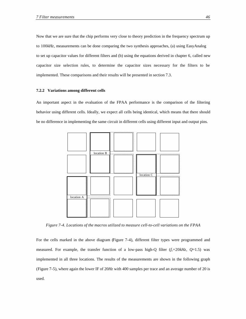
7 Filter measurements 46
Now that we are sure that the chip performs very close to theory prediction in the frequency spectrum up
to 100kHz, measurements can be done comparing the two synthesis approaches, (a) using EasyAnalog
to set up capacitor values for different filters and (b) using the equations derived in chapter 6, called new
capacitor size selection rules, to determine the capacitor sizes necessary for the filters to be
implemented. These comparisons and their results will be presented in section 7.3.
7.2.2 Variations among different cells
An important aspect in the evaluation of the FPAA performance is the comparison of the filtering
behavior using different cells. Ideally, we expect all cells being identical, which means that there should
be no difference in implementing the same circuit in different cells using different input and output pins.
location A
location C
location B
Figure 7-4. Locations of the macros utilized to measure cell-to-cell variations on the FPAA
For the cells marked in the above diagram (Figure 7-4), different filter types were programmed and
measured. For example, the transfer function of a low-pass high-Q filter (fc=20kHz, Q=1.5) was
implemented in all three locations. The results of the measurements are shown in the following graph
(Figure 7-5), where again the lower IF of 20Hz with 400 samples per trace and an average number of 20 is
used.

7 Filter measurements 47
Title: stat_lh20.epsCreator: MATLAB, The Mathworks, Inc.CreationDate: 03/30/98 19:29:11
Figure 7-5. Differences among utilized cells shown for a low-pass filter.
Taking the filter in location A as a reference curve (i.e. assuming that it has no error), we can compare the
same filters implemented in location B and C with the one implemented in A. Therefore the relative error,
which is shown in Figure 7-5b, gives a measure for how different the respective cells are. We can observe
in Figure 7-5b that the relative error in general is very small, although it grows for frequencies higher than
about 300kHz, in analogy to the very low amplitudes of the frequency response, where the signal consists
primarily of noise. Nevertheless, the maximum relative error among the three filters shown is less than
1% if we neglect the uncertainties at very low frequencies caused by instrument inaccuracies and
frequencies higher than 400kHz.
To further test the FPAA chip, similar measurements were done for a high-pass low-Q filter (f0=80kHz,
Q=0.9), but with less accuracy due to different analyzer settings as described above. This second set of
traces is shown in Figure 7-6.

7 Filter measurements 48
Title: hl80k9pr.epsCreator: MATLAB, The Mathworks, Inc.CreationDate: 03/09/98 18:39:22
Figure 7-6. Differences among utilized cells shown for a high-pass filter.
In the frequency response of the high-pass filters in general we observe a lot of noise in the stop-band. As
the magnitudes in this region are -50 dB or less, a big relative error has no practical significance.
Therefore, the relative error is shown starting only at a frequency of 3kHz. It can be seen from Figure 7-6
that the variations in the filter traces above noise level are in fact so small that they are practically
negligible.
To summarize the above results, we can say that within one cell the only deviations from z-domain theory
are expected for frequencies above 100kHz or 1/10fc. For frequencies in the range from DC to about
5kHz not all of the measurements performed here do provide data for reliable evaluation of FPAA
performance. Nevertheless, a few graphs show accuracy even down to 50Hz due to the higher effort in

7 Filter measurements 49
measurements as the intermediate frequency was decreased resulting in a very long sweep time.
Therefore, good behavior can be expected over the whole range for all filters.
As the observed variations among the random sample cells are extremely small, we don’t have to account
for these errors in the error model. In other words, these deviations are close to the accuracy limits
imposed by the error caused by the measurement setup. Therefore, from this point we assume identical
behavior of all the cells on one chip.
7.3 Comparison of capacitor size selection rules
In this section, filter measurements for low-pass, high-pass, band-pass, and notch filters are discussed. A
theoretical filter transfer function, called ideal, is taken and implemented on the FPAA according to
different synthesis approaches. In the following sections we try to find out which synthesis approach
using measurement results leads to more accurate filters in practice. We shall see through measurements
that computing the capacitor values according to the new rules results in most cases in a filter closer to
the specifications than the one designed using EasyAnalog. Errors due to all known error sources stated in
chapter 5 and 6, like necessary approximations in the design rules, quantization error, general capacitor
inaccuracies as well as measurement errors, comprise the deviations which are observed by comparing the
measured traces with the ideal function in the graphs.
7.3.1 Low-pass, low-Q filter measurements
In the following measurements, the implementations of the EasyAnalog design rules in comparison with
the rules developed in chapter 6 are compared. The first filter to be shown is a low-pass low-Q filter with
a corner frequency of 20kHz and pole quality factor of 0.6.

7 Filter measurements 50
Title: ll20k06.epsCreator: MATLAB, The Mathworks, Inc.CreationDate: 03/30/98 18:18:15
Figure 7-7. FPAA low-pass, low-Q filters ( f kHz Q0
20 0 6= =, . ) compared with ideal function
The traces in Figure 7-7 are taken with high accuracy to visualize the almost perfect filtering behavior of
the FPAA also at frequencies down to very low frequencies. In the error curves in Figure 7-7b we see a
smaller error for the filter set up with the new rules, especially in the frequency range below and above
the corner frequency. At exactly the corner frequency, EasyAnalog shows no error in the design. Using
the new capacitor size selection rules, the relative error falls below 5% for frequencies smaller than
200kHz and below 2% for frequencies <100kHz.
Figure 7-8 presents a low-pass, low-Q filter with a corner frequency fc=80kHz and pole quality factor
Q=1. Again, the measurements are taken with high accuracy for in the frequency spectrum above 300Hz,
so the error is significant.

7 Filter measurements 51
Title: ll80k1.epsCreator: MATLAB, The Mathworks, Inc.CreationDate: 03/30/98 18:31:56
Figure 7-8. FPAA low-pass, low-Q filters ( f kHz Q0 80 1= =, ) compared with ideal function
The curve shape of the relative error curve in Figure 7-8b shows very similar behavior as before. Again,
using EasyAnalog , we do not have a relative error at the corner frequency, but below and above there are
two extreme values in the error graph with a relative error around +/-10%. For the design approach using
the new rules, the relative error does not go higher than 3% for frequencies below 200kHz. The new rules
significantly improve the filtering behavior of the FPAA below this margin of 200kHz.
7.3.2 Low-pass, high-Q filter measurements
The first of the low-pass filter measurements, Figure 7-9, shows the behavior of the two low-pass, high-Q
synthesis approaches for a wanted corner frequency of 20kHz and a Q-factor of 1.5.

7 Filter measurements 52
Title: lh20k15.epsCreator: MATLAB, The Mathworks, Inc.CreationDate: 03/30/98 17:43:33
Figure 7-9. FPAA low-pass, high-Q filters ( f kHz Q0 20 1 5= =, . ) compared with ideal function.
In the graph of the frequency response in Figure 7-9a we can observe the inaccuracies for frequencies
below 300Hz which are caused by measurements. Neglecting these low frequency errors, we see from
Figure 7-9b that both implementations have no error up to 5kHz. In the frequency range below 100kHz,
the relative error of the new design method is constantly below +/-1%, whereas EasyAnalog introduces
an almost constant relative error in the range between 30kHz and 200kHz.
A further example of a low-pass, high-Q biquad filter to be realized shows Figure 7-10. Here, the filter
parameters are f0=50kHz and Q=5.

7 Filter measurements 53
Title: lh50k5.epsCreator: MATLAB, The Mathworks, Inc.CreationDate: 03/30/98 17:51:41
Figure 7-10. FPAA low-pass, high-Q filters ( f kHz Q0 50 5= =, ) compared with ideal function
The filter response plotted in Figure 7-10a is very smooth for frequencies higher than 300Hz. We do not
observe any errors for frequencies between 300Hz and 10kHz. The design with EasyAnalog shows
relative errors around the corner frequency of opposite sign to the errors occurring in the design using
the new capacitor size selection rules (Figure 7-10b). On the contrary to the filter set up using
EasyAnalog , especially for frequencies beyond the corner frequency, the filter obtained by the new
design rules shows a very small relative error.
The next measurements are all performed using a much shorter sweeping time, therefore the accuracy
especially for small signal frequencies suffers. But from previous measurements we know that the chip
performance is of the same high quality for frequencies up to 3-5kHz as before.

7 Filter measurements 54
7.3.3 High-pass, low-Q filter measurements
Measurements of high-pass, low-Q filter implementations on the FPAA are shown in the following graph,
Figure 7-11. The parameters for corner frequency and Q-factor are f kHz0 8= and Q = 0 6. .
Title: hl8k06.epsCreator: MATLAB, The Mathworks, Inc.CreationDate: 03/13/98 09:59:28
Figure 7-11. FPAA high-pass, low-Q filters ( f kHz Q0
8 0 6= =, . ) compared with ideal function.
In measured magnitude response traces we observe a very strongly “wobbling” curve for frequencies less
than 500Hz. These errors can be neglected because of the measurement inaccuracies up to frequencies of
3kHz, as was discussed in section 7.1. Nevertheless, it is very interesting to see that it is possible to
obtain a level of attenuation of around 50dB. More reliable quantitative interpretation is possible for
frequencies higher than 3kHz. Thus from Figure 7-11b we see that the error for the two synthesized
filters is decreasing up to the corner frequency. The synthesis error curve using new capacitor size
selection rules shows a very slight overshoot for increasing frequencies which turns into a negligible
error for frequencies from around 30kHz up to the half Nyquist frequency of 500kHz.

7 Filter measurements 55
The same filter type, this time incorporating a corner frequency of f kHz0 20= and a Q-factor of
Q = 0 707. , was implemented with the traces shown in Figure 7-12:
Title: hl20k1.epsCreator: MATLAB, The Mathworks, Inc.CreationDate: 03/13/98 10:12:33
Figure 7-12. FPAA high-pass, low-Q filters ( f kHz Q0 20 1= =, ) compared with ideal function.
The Figure 7-12 is only shown here as there is practically no error present for the design that uses the
new capacitor selection rules, whereas the filter developed using EasyAnalog shows an error higher
than 5% for frequencies lower than the corner frequency. Exactly at 20kHz, the relative error of the
EasyAnalog implementation has a zero transition with increasing error after that, turning into a very
small error for frequencies above 50kHz.
The next figure shows high-pass, low-Q filters with f kHz0 50= and Q = 0 9. (Figure 7-13).

7 Filter measurements 56
Title: hl50k09.epsCreator: MATLAB, The Mathworks, Inc.CreationDate: 03/13/98 10:24:20
Figure 7-13. FPAA high-pass, low-Q filters ( f kHz Q0
50 0 9= =, . ) compared with ideal function.
From Figure 7-13a we see that the dynamic range is quite high, as attenuation levels around 50dB can be
read off for low frequencies. The EasyAnalog error curve in Figure 7-13b shows almost a constant
magnitude of the relative error, with the error sign changing at the corner frequency 50kHz (zero error).
The error curve using the new capacitor size selection rules shows a big relative error at the beginning of
the displayed frequency interval around 3kHz, which is almost monotonously decreasing, and falls within
a virtual 5% line at 7kHz without changing its sign in the whole range. Therefore, the filter designed using
the new rules shows obviously a behavior much closer to the ideal function than the EasyAnalog filter
does.
A last sample of high-pass, low-Q measurements with f0=100kHz and Q=1 is given in Figure 7-14. Again,
we observe very high attenuation levels around 50dB in the stop-band. From the relative error curves in
Figure 7-14b we observe the same error behavior for low frequencies as is present for high frequencies in
the low-pass case. Here, the relative error for both synthesis approaches is very high, for the method
using new rules even higher than for the one employing EasyAnalog . The error curve decreases

7 Filter measurements 57
continuously, in the EasyAnalog case crossing the zero error line exactly at the corner frequency
f0=100kHz and falling further in the negative error range. For the filter set up using the new rules, there is
no zero transition, and for the half sampling frequency (500kHz) the error is zero.
Title: hl00k1.epsCreator: MATLAB, The Mathworks, Inc.CreationDate: 03/13/98 10:36:28
Figure 7-14. FPAA high-pass, low-Q filters ( f kHz Q0
100 1= =, ) compared with ideal function.
7.3.4 High-pass, high-Q filter measurements
The first high-pass, high-Q filters we will have a look at have a corner frequency f0=8kHz and a Q-factor
Q=2.5. Graphs of the magnitude responses in dB and the relative errors are shown in Figure 7-15a and b.

7 Filter measurements 58
Title: hh8k25.epsCreator: MATLAB, The Mathworks, Inc.CreationDate: 03/13/98 10:56:27
Figure 7-15. FPAA high-pass, high-Q filters ( f kHz Q0 8 2 5= =, . ) compared with ideal function.
As we can see from Figure 7-15b, the relative error for both, the EasyAnalog filter and the filter set up
using the new rules, is always within the bound +/-5% for the shown range from 2kHz up to 500kHz.
However, the filter designed using EasyAnalog has a slightly smaller error magnitude for frequencies
below 10kHz. Starting at frequencies between 10kHz and 20kHz, both synthesis approaches have an
identical error of almost constant magnitude.
A reason for the slightly better performance of the filter designed by EasyAnalog could be that the
quantization process involved has much less effect on the EasyAnalog capacitor values, which means
that the calculated values were in general closer to the ones that can be realized, unlike probably in the
case of the new capacitor size selection rules, where it is possible that the quantization error for several
capacitors is close to its maximum value.
Approaches to synthesize different high-pass, high-Q filters (f kHz Q0 50 2 5= =, . ) are shown in the
following graph, Figure 7-16:
7 Filter measurements 59
Title: hh50k25.epsCreator: MATLAB, The Mathworks, Inc.CreationDate: 03/13/98 11:13:05
Figure 7-16. FPAA high-pass, high-Q filters ( f kHz Q0 50 2 5= =, . ) compared with ideal function.
In Figure 7-16a, we see that the FPAA is as powerful as to attenuate a signal with 50dB. The relative error
graphs show two very different traces for the two synthesis methods. The design utilizing the new
capacitor size selection rules has almost no error around 3kHz, then it falls into the region of -5% and
remains almost constant up to 500kHz. The error curve obtained from the EasyAnalog approach in
comparison with the ideal curve shows two extreme values before and behind the corner frequency,
remarkable is the almost disappearing error for frequencies higher than 200kHz.
Unfortunately, it is not possible to compensate the error just by adding an offset value, as one could
wrongly conclude from the relative error graph in Figure 7-16b for the filter using new capacitor rules. As
the relative error is computed according to equation (7-1), we would need a linear curve proportional to
the frequency to compensate the error.
The next diagram shows the last high-pass, high-Q filter measurements presented here, trying to realize a
corner frequency of 100kHz and a Q-factor of 5.

7 Filter measurements 60
Title: hh00k5.epsCreator: MATLAB, The Mathworks, Inc.CreationDate: 03/13/98 11:41:09
Figure 7-17. FPAA high-pass, high-Q filters ( f kHz Q0 100 5= =, ) compared with ideal function.
The curves for the relative error in the above diagram, Figure 7-17, start with a high error, which falls
down to zero error between 10kHz and 20kHz. For the filter implemented using the new rules, the error is
quite small compared to EasyAnalog . EasyAnalog shows better behavior for frequencies starting
between 100kHz and 200kHz up to the half sampling frequency. It is worth mentioning that the relative
error for the filter computed with the new rules has a slightly lower corner frequency than expected, the
filter designed using EasyAnalog a slightly higher corner frequency. From this we conclude, that in
order to improve the filter, there is the potential for even better design rules which would synthesize a
filter with an exact corner frequency, as the capacitor values for both measured implementations are
totally different.
7.3.5 Band-pass, low-Q filter measurements
In the following graph, two possible FPAA implementations and the ideal magnitude response of a band-
pass, low-Q filter with a center frequency f kHz0 20= and a Q-factor Q = 0 707. are shown.

7 Filter measurements 61
Title: bl20k07.epsCreator: MATLAB, The Mathworks, Inc.CreationDate: 03/13/98 09:01:38
Figure 7-18. FPAA band-pass, low-Q filters ( f kHz Q0 20 0 707= =, . ) compared with ideal function.
From the above Figure 7-18a we can observe that the range of “smooth” filter operation starts around
3kHz with almost disappearing error. Below that frequency, where the magnitude levels are less than -
20dB, the measurement inaccuracy comes into play together with noise superimposed onto the highly
damped output signal. Both measurement traces, one where new capacitor size selection rules were used
as well as the one using the design rules implemented in EasyAnalog , show quite accurate behavior for
frequencies up to 20kHz. Furthermore, we see that the EasyAnalog trace is slightly more accurate in
that region, whereas the new capacitor size selection rules show better error behavior in the range from
20kHz to 100kHz. For higher frequencies, better performance of EasyAnalog is due to a turning point
in the error curve at the center frequency and the resulting zero crossing in its trace.
In Figure 7-19, a band-pass, low-Q filter with the parameters f kHz Q0 50 0 9= =, . is shown.

7 Filter measurements 62
Title: bl50k09.epsCreator: MATLAB, The Mathworks, Inc.CreationDate: 03/13/98 09:25:54
Figure 7-19. FPAA band-pass, low-Q filters ( f kHz Q0 50 0 9= =, . ) compared with ideal function.
In comparison with Figure 7-18a, the filters in Figure 7-19a show a similar dynamic range. Again there is
noise present, making the measurements less reliable for low frequencies. It is interesting to see that the
filter for a center frequency f0=50kHz is capable of attenuating the input signal with more than 30dB. The
general shape of the relative error curves in Figure 7-19b is not very different from the curves in Figure
7-18b. This time, however, the turning point at the corner frequency in the EasyAnalog error graph is
more obvious, as the relative error in positive as well as in negative direction is larger. For frequencies up
to 100kHz the new capacitor size rules evidently make a better filter.
For a band-pass filter with f0=100kHz and Q=1, there is no change in the dynamic range, as is seen from
Figure 7-20a below. Again, the error curve in Figure 7-20b for EasyAnalog has zero error at the center
frequency, although the error below and above 100kHz are quite significant. Applying the new capacitor
size selection rules, this filter shows very favorable behavior up to a signal range of 200kHz.

7 Filter measurements 63
Title: bl00k1.epsCreator: MATLAB, The Mathworks, Inc.CreationDate: 03/13/98 09:34:01
Figure 7-20. FPAA band-pass, low-Q filters ( f kHz Q0 100 0 9= =, . ) compared with ideal function.
7.3.6 Band-pass high-Q filter measurements
Unfortunately, it was not possible to set the capacitors for the synthesis approach using the new capacitor
size selection rules because the macro editor did not allow proper setting of capacitor values. However,
with a new version of the macro editor these measurements can be performed in a short time.
7.3.7 Band-stop, low-Q filter measurements
In the following, we will deal with band-pass, low-Q filters having different center frequencies and Q-
factors. In the first graph with measurements to be looked at, Figure 7-21, we try to implement the filter
with a center frequency of 20kHz and a Q-factor of 1.

7 Filter measurements 64
Title: sl20k1.epsCreator: MATLAB, The Mathworks, Inc.CreationDate: 03/13/98 14:04:10
Figure 7-21. FPAA band-stop, low-Q filters ( f kHz Q0
20 1= =, ) compared with ideal function.
In the above diagram, the most remarkable observation is a very high peak for the relative error in the
filter realized with new capacitor design rules as well as with the EasyAnalog rules. Obviously, the
dynamic range of the FPAA does not allow for such small signal magnitudes as the theoretical value
requires. The implemented notch is slightly wider than in the theoretical curve, as the relative error is
smaller than zero to the left and the right of the center frequency. At the center frequency, the magnitude
of the implemented filters is bigger than the theoretical value, because of the reason mentioned before
that we cannot realize the high attenuation factor imposed by the ideal filter.
But apart from the center frequency, the overall performance especially for the solid line filter is almost
perfect. For the frequencies not discussed yet below and above the center frequency, the error almost
disappears, whereas the EasyAnalog filter (represented by the dashed-dotted line) has a constant
negative relative error for higher frequencies.

7 Filter measurements 65
In the next graph, band-stop filters with an ideal center frequency f0=50kHz and Q-factor Q=0.9 are shown
(Figure 7-22).
Title: sl50k09.epsCreator: MATLAB, The Mathworks, Inc.CreationDate: 03/13/98 14:25:05
Figure 7-22. FPAA band-stop, low-Q filters ( f kHz Q0
50 0 9= =, . ) compared with ideal function.
Again, there is a high error peak present in Figure 7-22b. The EasyAnalog filter shows very sound
behavior around the center frequency, as the high peak can be explained using the same arguments as
before. Furthermore, we see that the notch is located exactly at the desired frequency due to a
symmetrical error around f0, on the contrary to the filter implemented according to the new rules. There,
the error is not symmetrical due to a slightly smaller center frequency than required.
At low frequencies, both, the EasyAnalog filter and the one using the new rules have only very little
error. The relative error of the EasyAnalog approach for frequencies above the center frequency is
quite high compared with the almost perfect new-rules filter, as the error in the first has a relatively high
magnitude (note the scale of relative error axis!) and is almost constant.

7 Filter measurements 66
The measurements of the last filter type presented here are band-stop filters with a corner frequency of
100kHz and a Q-factor of 0.707 (Figure 7-23).
Title: sl00k07.epsCreator: MATLAB, The Mathworks, Inc.CreationDate: 03/13/98 14:34:56
Figure 7-23. FPAA band-stop, low-Q filters ( f kHz Q0
100 0 707= =, . ) compared with ideal function.
In Figure 7-23 we can easily notice on the magnitude of the frequency response that the filter using the
new capacitor size selection rules leads an inaccurate solution in terms of the center frequency. Instead of
realizing the center at 100kHz, it must lie approximately around 90kHz. Therefore, the relative error has a
very high peak with asymmetrical side lobes. Although the behavior in the pass-band is quite good, the
filter designed using EasyAnalog is superior.
Again we can see from the band-stop measurements that there is still room for better design rules
incorporating the advantages of both, exact behavior at the center frequency as EasyAnalog can facilitate
or better behavior at high frequencies like in the design using the new rules.

7 Filter measurements 67
7.3.8 Band-stop high-Q filter measurements
Unfortunately, it was not possible to set all the capacitor values which are required for the band-stop,
high-Q filter because of the mentioned software problem. In all the previous designs there were eight or
less capacitor values to be adjusted, whereas here we are required to set the values of nine parameters.
This is not possible without the use of a properly functioning Macro Editor.

68
8 Analysis of results
8.1 Calculation of an overall error bound
In order to predict a worst case in the filtering behavior of the FPAA, we utilize the existing error model
to calculate an overall error bound. If all the measured error curves fall into the region below the error
bound curve, we can say that the error model holds.
To avoid the square root in the expression for the magnitude of the biquad filter transfer function, the
square of the magnitude of H jbiquad ( )w is calculated:
Q = =- + +
- + +H j
K K K
Q
biquad ( )( ) ( )
( ) ( )w
w w
w ww
w
22
2
0
2
1
2
2
0
2 2 0 2
. (8-1)
The given parameters K 2 , K1 , K 0 , w 0 , and Q in (8-1) cannot be realized with perfect accuracy as they are
themselves dependent on imperfect capacitors. Taking this into account, we calculate the deviation in Q ,
d ( )Q , which is due to the deviation in the coefficients, d K 2b g , d K1b g , d K 0b g , d w 0b g, d Qa f . According to
a first order Taylor approximation, the error bound equation becomes:
d∂∂
d∂∂
d∂∂
d∂∂ w
w d w∂∂
dQQ
Q Q Q Q Qa f b g b g b g b g a f= + + + +RS|T|
UV|W|1
2
2 2
1
1 1
0
0 0
0
0 0K
K KK
K KK
K KQ
Q Q .(8-2)
As mentioned before, the error in each coefficient is a function of all the errors in the capacitors
occurring in the respective coefficient equation. Therefore, formulas stating the error bound for each
coefficient can be obtained in the form:
d∂∂
d∂∂
d∂∂
d∂∂
d
∂∂
d∂∂
d∂∂
d∂∂
d
( ) ( ) ( ) ( ) ( )
( ) ( ) ( ) ( )
"
" "
'
' 'KK
K
CC C
K
CC C
K
CC C
K
CC C
K
CC C
K
CC C
K
CC C
K
CC C
A
A A
B
B B
2
2
2
1
1 12 2
1
1 12
3
3 3
2
1
1 12 2
4
4 42
2
2 2
1= + + +
RS|T|+
+ + + +UV|W|
(8-3)
d∂∂
d∂∂
d∂∂
d∂∂
d
∂∂
d∂∂
d
( ) ( ) ( ) ( ) ( )
( ) ( )
'
' 'KK
K
CC C
K
CC C
K
CC C
K
CC C
K
CC C
K
CC C
A
A A
B
B B1
1
1
1
1 11
3
3 31 1
1
4
4 41
2
2 2
1= + + +
RS|T|+
+ +UV|W|
(8-4)

8 Analysis of results 69
d∂∂
d∂∂
d∂∂
d∂∂
d
∂∂
d∂∂
d
( ) ( ) ( ) ( ) ( )
( ) ( )
KK
K
CC C
K
CC C
K
CC C
K
CC C
K
CC C
K
CC C
A
A A
B
B B0
0
0
1
1 10
3
3 30 0
0
4
4 40
2
2 2
1= + + +
RS|T|+
+ +UV|W|
(8-5)
d ww
∂w∂
d∂w∂
d∂w∂
d∂w∂
d∂w∂
d( ) ( ) ( ) ( ) ( ) ( )0
0
0
2
2 20
3
3 30 0 0
4
4 4
1= + + + +
RS|T|UV|W|C
C CC
C CC
C CC
C CC
C CA
A A
B
B B (8-6)
d∂∂
d∂∂
d∂∂
d∂∂
d∂∂
d( ) ( ) ( ) ( ) ( ) ( )QQ
Q
CC C
Q
CC C
Q
CC C
Q
CC C
Q
CC C
A
A A
B
B B= + + + +RS|T|
UV|W|1
2
2 2
3
3 3
4
4 4(8-7)
Fortunately, in both, high-Q and low-Q filter implementations, the same capacitor names are used, so the
above equations need to be written only once. However, when calculating actual error bound values, we
have to respect both cases due to the different definitions of the coefficients K2, K1, K0, w 0 , and Q.
It is important to mention here that the capacitor error model for a single capacitor can be simplified.
This is due to the fact that introducing the new capacitor size selection rules we have full control over the
actually required capacitor size in comparison to the size that can be implemented. In other words, we can
exclude the general quantization error as it is exactly known. The remaining relative error bound
expression for a single capacitor C l becomes then:
ds e
l( )( )
( )C ql u
ll = +1
. (8-8)
Intuitively, we realize that the different types of filters like low-pass, high-pass, band-pass and band-stop,
each of them once more split up into low-Q or high-Q implementation, must have different error bounds.
But in addition to that it can be seen already from (8-8) that each filter, i.e. each different set of capacitor
values, must have its own error bound. This is because the resulting equation is a function of the absolute
number of unit capacitors, l, which are incorporated to set up the needed capacitor value.
Substituting equation (8-8) for each different capacitor into the equations (8-3) to (8-7), and then
inserting the resulting equation into (8-2) gives the overall error bound for the magnitude square of the
biquad filter transfer function. Due to the extent of this single equation it is not shown here. However, this

8 Analysis of results 70
equation has been implemented for both, low-Q and high-Q filters, in the form of a Matlab program,
therefore allowing to compute the desired error bound for all desired sets of capacitors.
8.2 Definition of error in dB
Analogous to the representation of the filter transfer functions, a logarithmic approach is a sound
representation for the error bound.
In this paragraph we will introduce two different error terms which are especially useful in displaying the
error bound and comparing it with actual measurements. These two terms are (a) the magnitude error in
dB, called e dB , and (b) the magnitude error bound in dB, called D dB . We will use them in chapter 8.4 to
plot graphs to visualize the quality of the error model.
8.2.1 Magnitude error in dB
The magnitude error in dB, e dB , of the transfer function is calculated on the basis of the magnitude of the
measured transfer function, GM , and the magnitude of the exact transfer function G .
D DG G G G G GM M= - ¤ = + , (8-9)
where DG is the difference between measured and exact magnitude of the transfer function.
To be able to compare it with the positive error bound, we are only interested in the absolute value of the
logarithmic error:
e dB MG G= -20 20log log = 20 logG
GM =
+20 log
G G
G
D , (8-10)
or, expressed in slightly different terms using (8-9),
e dBMG G
G= +
-20 1log( ) ,
(8-11)
where G G
GM -
is the relative error of GM .

8 Analysis of results 71
8.2.2 Magnitude error bound in dB
To calculate the magnitude error bound in dB, D dB , we use the squared magnitude of the exact transfer
function F = G 2 and ~
maxF F DF= + .
The magnitude error bound is defined as follows:
D F FdB = -20 20log~
log , (8-12)
and because ~F F≥ always holds, we obtain
DFF
DFFdB = = +
FHG
IKJ10 10 1log
~
log max , (8-13)
or, again incorporating ~F ,
DF F
FdB = +-F
HGIKJ10 1log
~
,(8-14)
with ~F F
F-
being the relative error of ~F .
8.3 Error bound graphs
Using the introduced definition of the error bound in dB, sample error bound curves calculated from the
equations stated in chapter 8.1 will be shown, plotted in the form of three dimensional graphs.
Each capacitor in a set contributes with its appropriate value to the error bound. As the error bound
depends on statistical parameters, which are not exactly determined yet, it is interesting to observe how
the overall error bound changes varying the parameters s e( ) and l( )l . Unfortunately, we cannot display
the error bound as a function of frequency and both of the statistical values on the same plot. Therefore,
graphs for a sample low-pass filter are displayed, where either s e( ) is varied and l( )l is fixed or vice
versa.

8 Analysis of results 72
8.3.1 Low-Q filter error bound
The graph in Figure 8-1 shows the error bound when synthesizing a low-pass filter according to the new
capacitor size selection rules. As before, the corner frequency, f0, is 22.75kHz and the Q-factor equals
0.9, resulting in the following rounded capacitor values:
CA CB C1 C2 C3 C4 C1’ C1”
510 255 54 54 54 44 0 0
Table 8-1. Set of low-Q filter capacitor values for which the error bound was computed.
The parameter s e( ) varies in the range between 0 and 0.02, whereas l( )l is held constant at a typical value
of 0.0002.
Title: lq_sigma.epsCreator: MATLAB, The Mathworks, Inc.CreationDate: 03/24/98 21:30:41
Figure 8-1. Low-Q filter error bound with varying s e( ) .
We notice from Figure 8-1 that the error bound has a peak at a frequency around 20kHz and a minimum
close to 320kHz in the allowed frequency range from zero to 500kHz. The frequencies where these two
extreme values occur do not change with varying s e( ) , only the error bound in dB is scaled in magnitude

8 Analysis of results 73
with increasing s e( ) . The error bound is very close to zero for very small values of s e( ) / u and grows in
the maximum around 20kHz to a value higher than 0.5dB.
In the graph shown in Figure 8-2, the same filter parameters are utilized to calculate the error bound.
However, this time the parameter s e( ) / u is fixed at a typical value, s e( ) .= 0 005u and l( )l is varied in
the range from 0 to 0.001.
Title: lq_bias.epsCreator: MATLAB, The Mathworks, Inc.CreationDate: 03/24/98 19:39:05
Figure 8-2. Low-Q filter error bound with varying bias l( )l .
As can be seen from Figure 8-2, variation of the bias parameter l( )l around its typical value of 0.0002
does not cause a big change in the shape of the error bound. Although the bias error is roughly speaking
one order of magnitude smaller than s e( ) / u , we yet see that the influence on the magnitude of the error
bound is not negligible.
It can be said that s e( ) / u is the dominating factor as a small change in s e( ) causes a much bigger change
in the error bound than a small change in l( )l does. Apart from that, the error term incorporating s e( ) in

8 Analysis of results 74
equation (8-8) is explicitly dependent on the square root of the respective capacitor size, whereas l( )l is
not.
For different low-pass, low-Q filters the curve shape looks very similar, so in general at least a qualitative
statement about the shape of the overall error bound for this type of filter is possible. As already
mentioned, if the exact bound for a specific filter is needed, it has to be calculated incorporating the
respective capacitor values.
8.3.2 High-Q filter error bound
According to the evaluation of the error bound according to the equations (8-1) to (8-7) for high-Q filter
coefficients, a high-pass, high-Q filter is used for the demonstration of the overall error bound. The filter
parameters, which are implemented, belong to a high-pass filter with a corner frequency of 20kHz and a Q
factor of 1.5. The capacitor sizes are obtained by applying the respective new capacitor size selection
rules, yielding
CA CB C1 C2 C3 C4 C1’ C1”
267 267 0 33 33 174 0 255
Table 8-2. Set of high-Q filter capacitor values for which the error bound was computed.
Now, again the parameters in the capacitor error model equation (8-8) are varied, as these may vary due to
slight differences between different FPAA chips.
In the first graph, Figure 8-3, we vary s e( ) / u from 0 to 0.02, with l( )l is fixed at the typical value of
0.0002.

8 Analysis of results 75
Title: hq_sigma.epsCreator: MATLAB, The Mathworks, Inc.CreationDate: 03/24/98 20:24:59
Figure 8-3. High-Q filter error bound with varying s e( ) .
From Figure 8-3 in comparison with Figure 8-1 it can be observed that the general curve shape of low-Q
and high-Q error bound does not show very significant differences. However, in Figure 8-3 the maximum
around 20kHz is more acute than before, and there is no minimum detectable at higher frequencies close
to 320kHz. Starting around 40kHz, the error bound magnitude does not change with increasing
frequencies but remains constant.
In the next step, we keep the error model parameter s e( ) / u fixed at its typical value, s e( ) .= 0 005u ,
while l( )l is varied from 0 to 0.001. The filter is the high-pass, high-Q filter from before.

8 Analysis of results 76
Title: hq_bias.epsCreator: MATLAB, The Mathworks, Inc.CreationDate: 03/24/98 20:25:56
Figure 8-4. High-Q filter error bound with varying bias l( )l .
In the high-Q case we can observe the same as in the low-Q case. The parameter s e( ) in the error equation
has more influence on the overall magnitude of the error bound than the parameter l( )l has.
8.4 Comparison of error bounds and measurements
In chapter 5 the capacitor error model is described in detail. Now, as filter measurements are available
and the filter design errors are known, we can quantitatively compare the results. Using the definitions for
the logarithmic errors introduced in paragraph 8.2, a fair and sound comparison is possible.
It is important to mention that the ideal transfer function for calculating the measured error in dB in this
case is the transfer function obtained by z-domain analysis, bilinear transition to the s-domain and setting
the respective capacitor value(s) to zero according to the filter type.
For three example filters, the error bound curves are compared with the curve of the measured error and
displayed.

8 Analysis of results 77
8.4.1 Measured error and error bound for low-pass, low-Q filter
The well known sample low-pass, low-Q filter with f0=22.75kHz and Q=0.9 is used to show the measured
error and its error bound in one graph as an example for low-pass filters.
Title: ll2275k09ebd.epsCreator: MATLAB, The Mathworks, Inc.CreationDate: 03/25/98 11:10:53
Figure 8-5. Comparison of measured error and error bound of low-pass filter; f0=22.75kHz, Q=0.9.
In Figure 8-5 we see that the measured error is below the error bound for frequencies smaller than 20kHz.
For higher frequencies, the error grows above the 1dB point.
Figure 8-6 shows the error bound and the measured error for a high-pass high-Q filter with a corner
frequency of 8kHz and a Q-factor of 2.5.

8 Analysis of results 78
Title: hh8k25ebd.epsCreator: MATLAB, The Mathworks, Inc.CreationDate: 03/25/98 10:36:33
Figure 8-6. Comparison of measured error and error bound of high-pass filter; f0=8kHz, Q=2.5.
The high-pass filter shows a relatively small almost constant error with a high peak close to its corner
frequency 8kHz. What is different in comparison to the low-pass filter is that the error is relatively low
for frequencies above 100kHz. The relative error falls almost entirely below the given bound in the
frequency range below the corner frequency.
An example for a band-pass, low-Q filter is shown in Figure 8-7. The center frequency is 100kHz with a
Q-factor of 1.

8 Analysis of results 79
Title: bl00k1ebd.epsCreator: MATLAB, The Mathworks, Inc.CreationDate: 03/25/98 10:59:04
Figure 8-7. Comparison of measured error and error bound of band-pass filter; f0=100kHz, Q=1.
Again, we can observe Figure 8-7 that the actual error does not completely fall below the predicted error
bound. Only in the region between 40kHz and 100kHz we observe the expected behavior.
To summarize the observations above, roughly speaking we can say that the error in the measurements is
bigger than what we expect from the model. In other words, our error model does not hold. A suspected
reason for the failure of the existing model is that we have to deal with extremely small error magnitudes,
in general a sign for the good quality of the measurements. As can be seen from the above graphs for the
region from 3kHz to 100kHz, the error in dB falls almost wholly below 0.1dB. In general we know that
our error model does not account for the errors caused by the measuring process. So in a next step, the
accuracy of the network analyzer in the frequency band of our interest has to be determined. The
information obtained can be then used to show the region of uncertainty due to the measuring process. If

8 Analysis of results 80
this procedure still does not provide measured curves within the error bound, we have to consider another
source of error in the model.
As the filter response has a magnitude just above noise level in the stop-band, a higher error is justified in
that region. Therefore, it is very difficult to distinguish between signal magnitude and noise magnitude.
This would mean that the error model has to be extended, in other words we have to account for the errors
due to signals close to noise.
81
9 Discussion of other filter implementations
In this chapter some critical aspects of the switched capacitor technique are discussed. The most
important reason why we have to think about a different technique is the restriction to low frequencies
imposed by tiny capacitors which would be required. With higher frequencies, the necessary capacitors
immediately run into dimensions of the order of parasitic capacitances. Therefore, a totally different
technique is required as an alternative to switched capacitors.
9.1 Characterisation of s/c circuits
The following summary with a neutral characterization of switched capacitor circuits can be found in
[Toumazou, Hughes, Battersby 1993], where more details are included.
• Switched capacitor circuits usually make use of well-established active-RC circuit structures by
substitution of integrators. Therefore, its modularity and low sensitivity to component spreads can be
retained.
• The integrators execute algorithms defined by difference equations, thereby manipulating past and
present voltage samples. Low supply voltages necessarily imply degraded performance.
• Switched capacitor circuits are not totally compatible with digital VLSI processes due to the
capacitors needed.
• Switched capacitor circuits are split up in versatile building blocks which have a low design
interaction (loading of a module by other modules does not significantly change the module’s
performance). This means that the design can be automated due to its hierarchy.
9.2 Switched current technique
The switched current technique is a current-mode signal processing technique which utilizes the ability of
an MOS transistor to maintain its drain current when its gate is open-circuited, through the charge stored
on its gate oxide capacitance. Compared to switched capacitors, the switched current technique requires

9 Discussion of other filter implementations 82
only baseline VLSI CMOS processing, so no extra capacitor banks are needed. In general, the range of
applications is pretty much the same as for switched capacitors.
The technique itself is very old (first papers in 1972), but in the late 1980’s it was revived by different
researchers.
Switched current circuits, use current samples instead of voltage samples as is the case in switched
capacitor circuits. An analogy of both implementations is the fact that they are sampled circuits with time
discrete values, so switched current circuit operation can also be described with difference equations
yielding to z-domain analysis.
The general s/c integrator structure from Figure 4-5 is expressed in terms of a difference equation as
follows:
v nT v nT TC
Cv nT v nT T
C
Cv nT T
C
Cv nTout out
A A A
( ) ( ) ( ) ( ) ( ) ( )= - - + - + - -11 1
22
33 (9-1)
To incorporate a switched current system with the same function as the s/c network, we just have to
substitute in equation (9-1) all voltages by currents. This yields the equation
i nT i nT TC
Ci nT i nT T
C
Ci nT T
C
Ci nTout out
A A A
( ) ( ) ( ) ( ) ( ) ( )= - - - - + - -11 1
22
33 . (9-2)
In general, z-domain transform would yield a current transfer function identical to the sum of the voltage
transfer function in equations (4-10), (4-11), and (4-12).
From equation (9-2) we notice that for a realization of the integrator structure the following mathematical
operations on currents are needed: summation/subtraction, scaling and a delay module. Summation (or
subtraction) can be achieved by feeding the currents (or their inverse) into a low impedance circuit node.
Scaling can be accomplished using current mirrors. For the delay operation, however, we need a new
building block, called the current memory cell.

9 Discussion of other filter implementations 83
iin iout
Ibias
C
F1
F2
F1S
Figure 9-1. Single transistor current memory cell.
Figure 9-1 shows a current memory cell using only a single transistor. Its behavior can be described as
follows: when Φ1 goes high, the input current iin adds to the bias current Ibias, so the sum, Ibias+ iin flows
through the closed switch S and charges the discharged gate-source capacitor. Due to the charging
process, the gate-source voltage VGS increases, and when the threshold voltage is reached, the transistor
conducts. Once the capacitance is fully charged, the whole current Ibias+ iin flows into the drain of the
transistor.
At the end of Φ1, the value of VGS is held on the capacitor C and sustains the current Ibias+ iin in the drain,
even when during phase Φ2 switch S is opened. As the input switch is open during Φ2, no current can flow
through it, whereas the output switch conducts. Therefore, a current of the same magnitude as iin has to
flow from the output into the circuit to add up with the bias current to keep the drain current flowing. In
other words, during Φ2 an output current iout with the opposite sign of the current iin during Φ1 is forced to
flow.
Using the memory cell from Figure 9-1, it can easily be seen that cascading of two of those memory cells
with opposite clock phases comprise a delay cell which realizes a delay of the inverse clock frequency T.
[Toumazou, Hughes and Battersby 1993].

9 Discussion of other filter implementations 84
The advantage of this technology is that here we employ the parasitic gate oxide capacitance, whereas in
switched capacitor circuits we try to get rid of parasitics by special arrangements. As a result, in switched
current technology we eliminate large capacitors. In addition, much higher operating frequencies than
with switched capacitors should be possible according to theoretical considerations. However, due to the
lack of interest, switched current technology has not been very well explored, therefore it has not had a
breakthrough yet.
To implement a chip similar to the FPAA in switched current technology, it is necessary to have current
scaling devices with programmable scale factor. So in terms of realizing this idea, one would have to think
about programmable current mirrors or analog multipliers.

85
10 Conclusions and further research
In this work, the technology and behavior of a Field Programmable Analog Array implemented by
Motorola was described, analyzed, and evaluated experimentally.
An overview of the technology was given, followed by the theoretical background necessary to understand
and analyze s/c biquad filter structures. An error model for capacitors, introduced in [Palusinski et al.
1997a], was presented, and a new source of error, namely interconnect effects, was described
qualitatively.
Then detailed z-domain analysis was applied to the low-Q and high-Q implementations of s/c biquad
circuits, resulting in the proposal for new filter synthesis rules for low-pass, high-pass, band-pass, and
notch filters. The new synthesis approach states capacitor size selection rules for the occurring capacitors
in the circuit implementations based on the biquad filter parameters. In theory, these new rules proved by
far superior to the existing rules.
Measurements were taken to confirm the theory, allowing for fair comparison of the new filter synthesis
approach with the conventional method using EasyAnalogTM. Numerous filter implementations were
shown, and although not all filter showed significant improvements, the success of the new capacitor size
selection rules was clearly demonstrated.
Subsequently, an overall filter error bound based on the capacitor model was analytically derived and
compared with the actual error derived from measurements.
Finally, a rough idea with a different technique to implement a Field Programmable Analog Array was
sketched in the hope that the frequency limit imposed by the s/c realization could be moved to much
higher frequencies, which would increase the competitiveness of technology with digital signal
processors.

10 Conclusions and further research 86
Further research should include a quantitative extension of the capacitor error model by specifying the
term accounting for the interconnect capacitance effects presented. Apart from that, supplementary work
improving the FPAA capacitor size selection rules based on the above ideas could be very prolific and
increase the performance of filtering even more. From the error bound considerations, we see that more
accurate statistical information is necessary to derive reliable parameters for the capacitor error model.
This model can only be obtained either from the detailed knowledge of the process conditions or more
likely by sophisticated statistical capacitor error measurements.

87
11 References
Anderson, D., C. Birk, O. A. Palusinski, M. Spitz, K. Reiss. 1998. Interconnect Effects on
Performance of Field Programmable Analog Array. Accepted for presentation at: 2nd IEEE
Workshop "Signal Propagation on Interconnects" (SPI ’98) in Travemuende, Germany, May 13-18,
1998.
Birk, C. 1998. Evaluation of Filters implemented using a Field Programmable Analog Array. WMC
’98 - ICSEE, San Diego, California, Jan. 11-14, 1998.
Bronstein, I. N., K. A. Semendjajew. 1991. Taschenbuch der Mathematik. 25th ed. Stuttgart: B. G.
Teubner. ISBN 3-8154-2000-8.
Gregorian, R., G. C. Temes. 1986. Analog MOS Integrated Circuits for Signal Processing. New York:
John Wiley & Sons. ISBN 0-471-09797-7.
Huelsman, L. P. 1993. Active and Passive Analog Filter Design. New York: McGraw-Hill. ISBN 0-07-
030860-8.
Johns, D. A., K. W. Martin. 1997. Analog integrated circuit design. New York: John Wiley & Sons.
ISBN 0-471-14448-7.
Kammeyer, K. D., K. Kroschel. 1996. Digitale Signalverarbeitung - Filterung und Spektralanalyse.
3rd ed. Stuttgart: B. G. Teubner, ISBN 3-519-26122-7.
Moschytz, G. S. 1984. MOS Switched-Capacitor Filters: Analysis and Design. New York: IEEE Press.
ISBN 0-87942-177-0.
Motorola. 1997a. EasyAnalogTM Design Software User’s Manual. Motorola, Inc. 1997.
Motorola. 1997b. Field Programmable Analog Array MPAA020. Advance Information. Semiconductor
Technical Data. Motorola, Inc. 1997.

11 References 88
Motorola. 1997c. Field Programmable Analog Array Evaluation Board. Advance Information.
Semiconductor Technical Data. Motorola, Inc. 1997.
Motorola. 1997d. Introducing Motorola’s Field Programmable Analog Array. Semiconductor
Technical Summary. Motorola, Inc. 1997.
Palusinski, O. A., D. M. Gettman, D. Anderson, H. Anderson, C. Marcjan. 1997a. Filtering
Applications of Field Programmable Analog Arrays. Journal of Circuits, Systems and Computers.
World Scientific Pub. (in revision).
Palusinski, O. A., D. M. Gettman, M. Spitz, A. Huber, D. Anderson, C. Marcjan. 1997b. Evaluation
of Capacitor Errors in Field Programmable Analog Arrays with Switched Capacitor Circuits.
Journal of Circuits, Systems and Computers. World Scientific Pub. (in revision).
Sedra, A. S., K. C. Smith. 1991. Microelectronic Circuits. 3rd ed. New York: Oxford University Press.
Toumazou, C., J. B. Hughes, N. C. Battersby. 1993. Switched-Currents - An Analogue Technique for
Digital Technology. IEE Circuits and Systems Series. Peter Peregrinus. Chapter 3.
Van Valkenburg, M. E. 1982. Analog Filter Design. New York: Holt, Rinehart and Winston. ISBN 0-
03-059246-1.