m.sc. semester iv paper iii; unit i microprocessor 8085
TRANSCRIPT

Saikumar Chirra @ ECC - PrayagrajBy
Sources:- 1. Microprocessor 8085 – Ramesh Gaonkar
2. A course on 8085 Microprocessor – Prentice Hall
3. Microprocessors & its applications – P Raja
4. Microprocessor and Microcontroller Architecture and Interfacing
(Wikipedia)
M.Sc. Semester – IV
Paper – III; Unit – I
Microprocessor 8085 & Programs

Content :
1) Introduction to Microprocessor 8085
2) Architecture of Microprocessor 8085
3) Instruction set and
4) Simple programs

1) Introduction to Microprocessor 8085
Microprocessor is a Central Processing Unit (CPU) etched on a single chip.
A single Integrated Circuit (IC) has all the functional components of a CPU namely
Arithmetic Logic Unit (ALU), Control Unit and registers.
The 8085 microprocessor is an 8-bit processor that includes on its chip most of the logic
circuitry for performing computing tasks and for communicating with peripherals.

Features
8 bit microprocessor(8085 microprocessor can read or write or perform arithmetic and logical operations on 8-bit data at time)
It has 8 data lines and 16 address lines hence capacity is 216 = 64 kB of memory
Cock frequency is 3 MHz
It requires +5V power supply.
It is a single chip NMOS device implemented with 6200 transistors.
It provides 74 instructions with five addressing modes.
It provides 5 hardware interrupt and 8 software interrupts.
1. Introduction to …. Continue

Processor System Architecture
The typical processor system
consists of:
▪ CPU (central processing unit)
▪ ALU (arithmetic-logic unit)
▪ Control Logic
▪ Registers, etc…
▪ Memory
▪ Input / Output interfaces
Interconnections between these
units:
▪ Address Bus
▪ Data Bus
▪ Control Bus
1. Introduction to …. Continue
Bus and CPU
Bus: A shared group of wires used for
communicating signals among devices
• address bus: the device and the location within
the device that is being accessed
• data bus: the data value being communicated
• control bus: describes the action on the address
and data buses
CPU: Core of the processor, where instructions
are executed
• High-level language: a = b + c
• Assembly language: add r1 r2 r3
• Machine language: 0001001010111010101

Memory and I/O
Memory: Where instructions (programs) and data are stored
• Organized in arrays of locations (addresses), each storing
one byte (8 bits) in general
• A read operation to a particular location always returns the
last value stored in that location
I/O devices: Enable system to interact with the world
• Device interface (a.k.a. controller or adapter) hardware
connects actual device to bus
• The CPU views the I/O device registers just like
memory that can be accessed over the bus. However,
I/O registers are connected to external wires, device
control logic, etc.
• Reads may not return last value written
• Writes may have side effects
1. Introduction to …. Continue

2) Architecture of Microprocessor 8085
I. 8085 ARCHITECTURE
II. FUNCTION OF EACH BLOCK
III. 8085 BUS ORGANIZATION AND STRUCTURE

I. 8085 ARCHITECTURE (OR) BLOCK DIAGRAM
2). Architecture… Continue…

9
I. Intel 8085 CPU Block Diagram2). Architecture… Continue…
ALU
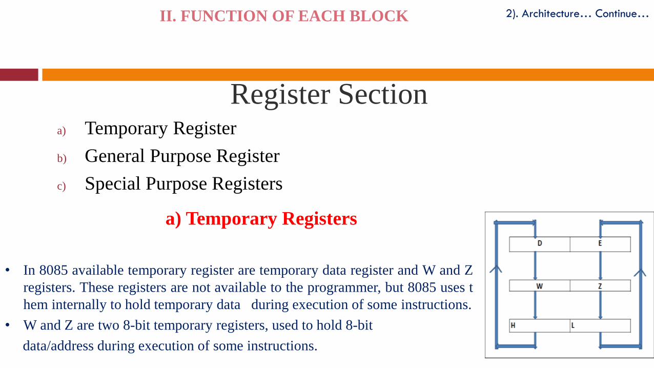
Register Sectiona) Temporary Register
b) General Purpose Register
c) Special Purpose Registers
a) Temporary Registers
• In 8085 available temporary register are temporary data register and W and Z
registers. These registers are not available to the programmer, but 8085 uses t
hem internally to hold temporary data during execution of some instructions.
• W and Z are two 8-bit temporary registers, used to hold 8-bit
data/address during execution of some instructions.
2). Architecture… Continue…II. FUNCTION OF EACH BLOCK

b). General Purpose Registers
B,C,D,E,H &L are used as general purpose register.
Each 8 bit long .
Apart from the above function these registers can also be used to work in pairs to
hold 16-bit data.
They can work in pairs such as B-C, D-E and H-L to store 16-bit data.
The H-L pair works as a memory pointer.
A memory pointer holds the address of a particular memory location.
They can store 16-bit address as they work in pair.
2). Architecture… Continue…II. FUNCTION OF EACH BLOCK

c). Special Purpose Register i. Accumulator
ii. Status or Flag Register
iii. Instruction Register
iv. Program Counter
v. Stack Pointer
i. Accumulator
• The accumulator is an 8-bit register that is a part of arithmetic/logic unit (ALU).
• This register is used to store 8-bit data and to perform arithmetic and logical operatio
ns.
• The result of an operation is stored in the accumulator. The accumulator is also ident
ified as register A.
• It also works as a via register for I/O accesses i.e. it reads data from input device and
similarly can transfer data to output device.
2). Architecture… Continue…II. FUNCTION OF EACH BLOCK

ii. Status or Flag Register
Flag register is a group of flip flops used to give status of different operations result.
The flag register is connected to ALU.
Once an operation is performed by ALU the result is transferred on internal data bus and status
of result will be stored in flip flops.
They are called Zero (Z), Carry (CY), Sign (S), Parity (P), and Auxiliary Carry (AC) flags.
A flag register contains a number of flags either to indicate certain conditions arising
after arithmetic and logical operations or to control certain operations.
2). Architecture… Continue…II. FUNCTION OF EACH BLOCK

The flags which indicate conditions are known as condition flags. The flags which are used to control certain
operations are called control flags.
A flag is a flip-flop which is set or reset by the processor to indicate certain conditions or set/reset by the
programmer to control certain operations.
• Carry flag(CY): If an operation performed in ALU generates the carry from D7 to next stage then CY flag is s
et, else it is reset.
• Auxiliary carry(AC): If an operation performed in ALU generates the carry from lower nibble (D0 to D3) to
upper nibble (D4 to D7) AC flag is set, else it resets.
• Zero flag(z): If an operation performed in ALU results 0value of entire 8-bits then zero flag is set, else it resets
• Sign flag(s): If MSB bit =0 then the number is positive, else it is negative.
• Parity flag(p):If the result contains even no. of ones this flag is set and for odd no. of ones this flag is reset.
2). Architecture… Continue…
ii. Status or Flag Register
II. FUNCTION OF EACH BLOCK

iii. Instruction Register
Temporary store for the current instruction of a program. Latest instruction sent here
from memory prior to execution. Decoder then takes instruction and decodes or interprets
the instruction. Decoded instruction then passed to next stage.
Instruction register is 8-bit register just like every other register of
microprocessor. Consider an instruction. The instruction may be anything like adding two
data's, moving a data, copying a data etc. When such an instruction is fetched from memory,
it is directed to Instruction register. So the instruction registers are specifically to store the
instructions that are fetched from memory.
There is an Instruction decoder which decodes the information's present in the Instruction
register for further processing.
2). Architecture… Continue…II. FUNCTION OF EACH BLOCK

iv. Program Counter
This 16-bit register deals with sequencing the execution of
instructions.
This register is a memory pointer.
Memory locations have 16-bit addresses, and that is why this is a 16-bit
register.
The microprocessor uses this register to sequence the execution of the
instructions.
The function of the program counter is to point to the memory address
from which the next byte is to be fetched. When a byte is being fetched,
the program counter is incremented by one to point to the next memory
location
2). Architecture… Continue…II. FUNCTION OF EACH BLOCK

v. Stack Pointer
The stack pointer is also a 16-bit register used as a memory pointer. It points to a memorylocation in R/W memory, called the stack. The beginning of the stack is defined by loading 16-bit address in the stack pointer.
Stack pointer is also a 16-bit register which is used as a memory pointer.
A stack is nothing but the portion of RAM (Random access memory).
Stack pointer maintains the address of the last byte that is entered into stack.
Each time when the data is loaded into stack, Stack pointer gets decremented.
Conversely it is incremented when data is retrieved from stack
2). Architecture… Continue…II. FUNCTION OF EACH BLOCK

ALU
The ALU performs the actual numerical and logic operation such as add,subtract, AND, OR, etc. Uses data from memory and from Accumulator toperform arithmetic. Always stores result of operation in Accumulator.
It is not accessible by user.
The word length of ALU depends upon of an internal data bus.
IT is 8 bit. It is always controlled by timing and control circuits.
It provides status or result of flag register.
2). Architecture… Continue…II. FUNCTION OF EACH BLOCK

Arithmetic and Logical Section
i. Instruction Decoder and Machine cycle Encoder
ii. Address Buffer
iii. Address/Data Buffer
iv. Increment/Decrement Address Latch
v. Interrupt Control
vi. Serial I/O Control Group
vii. Timing And Control
2). Architecture… Continue…II. FUNCTION OF EACH BLOCK

Instruction Decoder and Machine cycle Encoder
It accepts an OPCODE from instruction register, decodes it and gives
the decoded information to control logic.
The information includes what operation is to be performed, who is
going to perform it, etc. It means it will understand the instruction in
this block.
The decoded information is given to the timing and control unit that
provides control signals
2). Architecture… Continue…II. FUNCTION OF EACH BLOCK

Address Buffer
The contents of the stack pointer and program counter are loaded into the address buffer and address-data buffer.
These buffers are then used to drive the external address bus and address-data bus.
As the memory and I/O chips are connected to these buses, the CPU can exchange desired data to thememory and I/O chips.
The address-data buffer is not only connected to the external data bus but also to the internal data buswhich consists of 8-bits.
The address data buffer can both send and receive data from internal data bus.
The contents of the stack pointer and program counter are loaded into the address buffer and address-data buffer. These buffers are then used to drive the external address bus and address-data bus. As thememory and I/O chips are connected to these buses, the CPU can exchange desired data to the memoryand I/O chips.
The address-data buffer is not only connected to the external data bus but also to the internal data buswhich consists of 8-bits. The address data buffer can both send and receive data from internal data bus.
2). Architecture… Continue…II. FUNCTION OF EACH BLOCK

Increment/Decrement Address Latch
The 8-bit contents of a register or a memory location can be
incremented or decremented by 1.
This 16-bit register is used to increment or decrement the content of
program counter and stack pointer register by 1.
Increment or decrement can be performed on any register or a memory
location.
2). Architecture… Continue…II. FUNCTION OF EACH BLOCK

Interrupt Control
Consider that a microprocessor is executing the main program. Now wheneverthe interrupt signal is enabled or requested the microprocessor shifts thecontrol from main program to process the incoming request and after thecompletion of request, the control goes back to the main program.
For example an Input/output device may send an interrupt signal to notify thatthe data is ready for input. The microprocessor temporarily stops theexecution of main program and transfers control to I/O device. Aftercollecting the input data the control is transferred back to main program.
2). Architecture… Continue…II. FUNCTION OF EACH BLOCK

Serial I/O Control Group
The data transferred on to data bus is parallel data, but under
some conditions it is advantageous to use serial data transfer at
that time this control group is brought into application.
The input and output of serial data can be carried out using 2
instructions in 8085:
1. SID-Serial Input Data
2. SOD-Serial Output Data
2). Architecture… Continue…II. FUNCTION OF EACH BLOCK

Timing And Control
Timing and control unit is a very important unit as it synchronizes the registers and flow of data through
various registers and other units.
It accepts data from instruction decoder and generates micro steps to perform it ,in addition it accepts clock
inputs for synchronizing operations.
This unit consists of an oscillator and controller sequencer which sends control signals needed for internal and
external control of data and other units.
1. Control Signals: READY, RD(bar), WR(bar), ALE
2. Status Signals: S0, S1, IO/M(bar)
3. DMA Signals: HOLD, HLDA
4. RESET Signals: RESET IN(bar), RESET OUT.
2). Architecture… Continue…II. FUNCTION OF EACH BLOCK

Bus Organization
What is a Bus?
It is a set of pins, wires or signals having common functions asbus.
What is system Bus?
A bus is a bundle of wires that are grouped together to serve asingle purpose in microprocessor, generally there are three setsof communication lines that are called buses.
They are address bus, the data bus and control bus.
2). Architecture… Continue…
III. 8085 BUS ORGANIZATION AND STRUCTURE

Bus Structure
2). Architecture… Continue…
System Bus :-wires connecting memory &
I/O to microprocessor
Address Bus
Unidirectional
Identifying peripheral or memory location
Data Bus
Bidirectional
Transferring data
Control Bus
• Synchronization signals
• Timing signals
• Control signal

System Bus :-wires connecting memory &
I/O to microprocessor
Address Bus
Unidirectional
Identifying peripheral or memory location
Data Bus
Bidirectional
Transferring data
Control Bus
• Synchronization signals
• Timing signals
• Control signal
2). Architecture… Continue…

Address Bus
The bus over which the microprocessor sends out the address of a
memory location or I/O location is called as the address bus.
In 8085 microprocessor, Address bus is of 16 bits. This means that
Microprocessor 8085 can transfer maximum 16 bit address which
means it can address 65,536 different memory locations.
This bus is multiplexed with 8 bit data bus. So, the most significant
bits (MSB) of address goes through Address bus and LSB goes
through multiplexed data bus.
In 8085 address bus is 16 bit A0 –A15
2). Architecture… Continue…

Data Bus
It is bi-directional as Microprocessor requires to send orreceiver data. The data bus also works as bus in 8 bits long.
A data bus simply carries data. Internal buses carryinformation within the processor, while external buses carrydata between the processor and the memory. Typically, thesame data bus is used for both read/write operations.
When it is a write operation, the processor will put the data onto the data bus. When it is the read operation, the memorycontroller will get the data from the specific memory blockand put it in to the data bus.
The data bus in8085 is of 8 parallel lines D0 – D7
2). Architecture… Continue…

Control Bus
The control bus is used for sending control signals to the memory and
I/O devices. The CPU sends control signal on the control bus to enable
the outputs of addressed memory devices or I/O port devices.
Some of the control bus signals are as follows:
1.Memory read
2.Memory write
3.I/O read
4.I/O write.
2). Architecture… Continue…

32
The 8085 MP Instruction set has 74 operation codes that results in 246 instructions.
The set includes all the 8080A instructions plus two additional (SIM & RIM related to serial
I/O) instructions.
There are 5 different kinds of I-sets:-
1. Data transfer/copy I-set:
2. Arithmetic I-set:
(*ADD *SUB *INR (increment1) *DCR (decrement1)
3. Logic and Bit Manipulation I-set:
*AND (ANA/I) *OR (ORA/I) *X-OR (XRA/I) *Compare(CMP/CPI)
4. Branch I-set:
5. Stack, Input/output and Machine control I-set:
3) Instruction set of 8085

33
Instruction format
Instructions typically consist of
Opcode (Operation Code)
◼ defines the operation to be performed (e.g. opcode for ADD B is 80H)
(Source/Destination) Operand
◼ what’s being operated on (e.g. In instruction MOV A, B the registers A (Destination) & B (Source) are
operabds)
The 8085 Instruction set typically have 0, 1 or 2 operands and consists of one,
two and three byte instructions. The first byte is always opcode.
(Writing a program using IS)
OpCode (1 byte) OpCode(1 byte)
OpCode (1 byte) Opd2 (1 byte)Opd1 (1 byte)
Opd (1 byte)
3. Instruction set Conti…

One-byte Instructions
Includes Opcode and Operand
in the same byte
Opcode Operand Binary Code Hex Code
MOV C, A 0100 1111 4FH
ADD B 1000 0000 80H
HLT 0111 0110 76H
Opcode Operand Binary Code Hex Code
MVI A, 32H 0011 1110
0011 0010
3EH
32H
MVI B, F2H 0000 0110
1111 0010
06H
F2H
Opcode Operand Binary Code Hex Code
LXI H, 2050H 0010 0001
0101 0000
0010 0000
21H
50H
20H
LDA 3070H 0011 1010
0111 0000
0011 0000
3AH
70H
30H
Two-byte Instructions
First byte specifies Operation Code
Second byte specifies Operand
Examples-
Three-byte Instructions
First byte specifies Operation
Code
Second & Third byte specifies
Operand
Examples-

35
Example (AVR instruction)
Subtraction with carry
Syntax: sbc Rd, Rr
Operation: Rd ← Rd – Rr – C
Rd: Destination register. 0 d 31
Rr: Source register. 0 r 31, C: Carry
Instruction format
OpCode uses 6 bits (bit 10 to bit 15).
Two operands share the remaining 10 bits.
0 0 0 0 1 0 r d r r r rd d d d
015
3. Instruction set Conti…

36
Instruction lengths
The number of bits an instruction has
For some machines – instructions all have the same length
E.g. MIPS machines
For other machines – instructions can have different lengths
E.g. M68K machine
3. Instruction set Conti…

37
Instruction encoding
Operation Encoding
2n operations needs at least n bits
Operand Encoding
Depends on the addressing modes and access space.
◼ For example: An operand in direct register addressing mode requires at most 3 bits if the the number of registers it can be stored is 8.
With a fixed instruction length, more encoding of operations means less available bits for encoding operands
Tradeoffs should be concerned
3. Instruction set Conti…
38
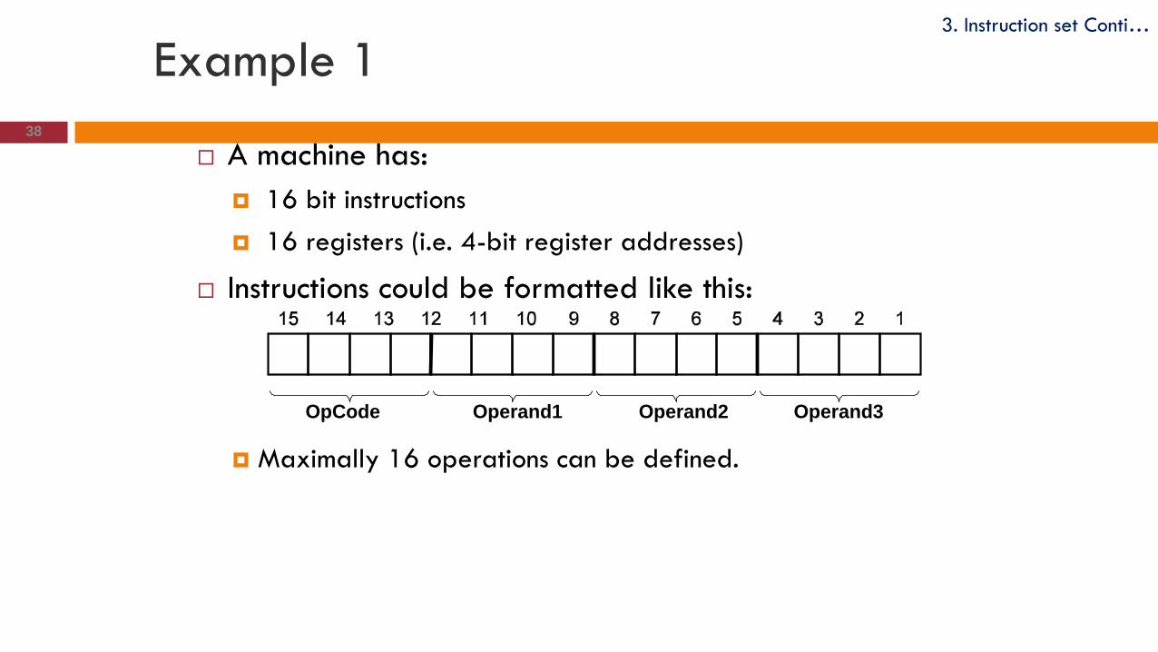
Example 1
A machine has:
16 bit instructions
16 registers (i.e. 4-bit register addresses)
Instructions could be formatted like this:
Maximally 16 operations can be defined.
OpCode Operand1 Operand2 Operand3
3. Instruction set Conti…

39
4) Simple programs
Program:
It is a sequence of instructions written to do specific task.
It instructs the microprocessor to perform a specific function.
Microprocessor understands Machine Language only!
Microprocessor cannot understand a program written
in Assembly language
A program known as Assembler is used to convert a
Assembly language program to machine language
Assembly
Language
Program
Assembler
Program
Machine
Language
Code

Assembly language program
to add two numbers
MVI A, 2H ;Copy value 2H in register A
MVI B, 4H ;Copy value 4H in register B
ADD B ;A = A + B
Note:
Assembly language is specific to a given
processor
For e.g. assembly language of 8085 is
different than that of Motorola 6800
microprocessor
Assembly Language of 8085
It uses English like words to
convey the action/meaning
called as MNEMONICS
For e.g.
MOV to indicate data transfer
ADD to add two values
SUB to subtract two values
4. Simple programs Conti…..

Graphic symbols used in the flow charts
4. Simple programs Conti…..

Steps in Assembly Language Program
Steps to write a program
Analyze the Problem
Sample Problem
Make a Flowchart
Write program Instructions using Assembly language of 8085
4. Simple programs Conti…..
Memory
Address (Hex)
Label Instruction Comments
Opcode Operands
XX00 As per need MOV B, C Move data from C register to B register
XX01 MOV A, M Move data from memory location M to
A register
Ex:
Program Format:

1. Program:
Add two 8-bit numbers and store 8-bit result in register C.
Analyze the Problem◼ Addition of two 8-bit numbers to be done
Sample Problem◼ Add two numbers
◼ Store result in register C
◼ Example
10011001 (99H) A
+00111001 (39H) D
11010010 (D2H) C
4. Simple programs Conti…..

Make a Flowchart:Start
Load Registers D, E
Copy D to A
Add A and E
Copy A to C
Stop
• Load 1st no. in register D
• Load 2nd no. in register E
• Copy register D to A
• Add register E to A
• Copy A to register C
• Stop processing
4. Simple programs Conti…..

Program
4. Simple programs Conti…..
Memory
Address: Opcode: Operands: Comments:
MVI D, 2H ; Load 1st no. in register D
MVI E, 3H ; Load 2nd no. in register E
MOV A, D ; Copy register D to A
ADD E ; Add register E to A
MOV C, A ; Copy A to register C
HLT ; Stop processing

2 Program:
Add two 8-bit numbers. Result can be more than 8-bits (Use Carry).
Sample Problem
◼ Example
10011001 (99H) A
+10011001 (99H) B
100110010 (132H)
◼ The 9th bit in the result is called CARRY bit.
4. Simple programs Conti…..
Analyze the Problem
Result of addition of two 8-bit
numbers can be 9-bit

0
How 8085 does it?
Adds register A and B
Stores 8-bit result in A
SETS carry flag (CY) to indicate carry bit
10011001
10011001
A
B
+
99H
99H
10011001 A1
CY
00110010 99H32H
4. Simple programs Conti…..
Storing result in Register memory
10011001
A
32H1
CY
Register CRegister B
Step-1 Copy A to C
Step-2
a) Clear register B
b) Increment B by 1

Make a Flowchart
Start
Load Registers D, E
Copy D to A
Add A and E
Copy A to CStop
Is
Carry = 1 Clear B
Increment B
No
4. Simple programs Conti…..
Yes

Program
4. Simple programs Conti…..
Memory Mnemonics (OR)
Address: Opcode: Operands: Comments:
MVI D, 2H ; Load 1st no. in register D
MVI E, 3H ; Load 2nd no. in register E
MOV A, D ; Copy register D to A
ADD E ; Add register E to A
MOV C, A ; Copy A to register C
JNC END ; Use Conditional Jump instructions
MVI B, 0H ; Clear register B
INR B ; Increment B
HLT ; Stop processing

3 Program:
Calculate the sum of series of numbers. The length of the series is in memory location 2300H and series itself begins from memory
location 2301H. The result of sum is stored in memory location 2500H and the carry is stored on location 2501H.
Sample Problem
◼ Example
2300H = 04H
2301H = 9AH
2302H = 52H
2303H = 89H
2304H = 3EH
Result = 9A + 52 + 89 + 3E = 1B3 (1 will be carry )
2500H = B3H 2501H = 01H
4. Simple programs Conti…..
Analyze the Problem
Let data of 4 numbers in 2301H to 23004H
Result 2500H and carry in 2501H

Make a Flowchart
Start
Sum = Sum + Pointer
Carry = Carry + 1
Stop
No
4. Simple programs Conti…..
Yes
Sum = 0
Carry = 0
Pointer = 2301
Count = (2300H)
Is
Carry = 1
Pointer = Pointer + 1
Counter = Counter - 1
No
Yes
Is
Count = 0
Load (2500H) = Sum
(2501H) = Carry

Program
4. Simple programs Conti…..
Memory
Address: Opcode: Operands: Comments:
LDA 2300H
MOV C, A ; Initialize counter
LXI H, 23001H ; Initialize pointer
SUB A ; Sum = 0
MOV B, A ; Initialize carry = 0
BACK : ADD M ; Sum (L) = Sum + data
JNC Loop ; Check Carry
INR B ; Add carry
Loop : INX H ; Increment Pointer
DCR C ; Decrement counter
JNZ Back ; Check if counter not 0 repeat
STA 2500H ; Store Sum
MOV A, B
STA 2501H ; Store Carry
HLT ; Stop processing

4 Program: Write an assembly language program in 8085 microprocessor to find maximum and
minimum of 10 numbers.
Sample Problem
1. Maximum number is stored in B register and minimum in C register
2. Load counter in D register
3. Load starting element in Accumulator, B and C register
4. Compare Accumulator and B register
5. If carry flag is not set then transfer contents of Accumulator to B. Else, compare Accumulator with
C register, if carry flag is set transfer contents of Accumulator to C
6. Decrement D register
7. If D>0 take next element in Accumulator and go to point 4
8. If D=0, store B and C register in memory
9. End of program
4. Simple programs Conti…..
Analyze the Problem
List of numbers from 2050H to 2059H and output at 2060H and 2061H.

ADDRESS LABEL INSTRUCTION COMMENT
2000H LXI H, 2050H Load starting address of list
2003H MOV B, M Store maximum
2004H MOV C, M Store minimum
2005H MVI D, 0AH Counter for 10 elements
2007H LOOP MOV A, M Retrieve list element in Accumulator
2008H CMP B Compare element with maximum number
2009H JC MIN Jump to MIN if not maximum
200CH MOV B, A Transfer contents of A to B as A > B
200DH MIN CMP C Compare element with minimum number
200EH JNC SKIP Jump to SKIP if not minimum
2011H MOV C, A Transfer contents of A to C if A < minimum
2012H SKIP INX H Increment memory
2013H DCR D Decrement counter
2014H JNZ LOOP Jump to LOOP if D > 0
2017H LXI H, 2060H Load address to store maximum
201AH MOV M, B Move maximum to 2060H
201BH INX H Increment memory
201CH MOV M, C Move minimum to 2061H
201DH HLT Halt
Draw the Flow
Chart ?
