n94 -18352 - nasa -18352 4.3.1 technology, ... formed on an n-channel junction of a twin-tub cmos...
TRANSCRIPT

3rd NASA Symposium on VLSI Design 1991
N94 -183524.3.1
Technology, Design, Simulation,and Evaluation for SEP-Hardened Circuits
J. R. Adams, D. AUred, M. Barry, and P. Rudeck,
R. Woodruff, J. Hoekstra, and It. Gardner
United Technologies Microelectronics Center
1575 Garden of the Gods Road
Colorado Springs, CO 80907
Abstract- This paper describes the technology, design, simulation, and evalu-
ation for improvement of the $EP hardness of gate-array and SRAM cells.
Through the use of design and processing techniques, it is possible to achieve
an SEP error rate less than 1.0E-10 errors/blt-day for a 90worst-case geosyn-
chronous orbit environment.
1 Single Event Upset
Single Event Phenomenon (SEP) occurs when a particle or heavy ion interacts with the
silicon, depositing charge on critical circuit nodes, causing data loss. Devices that retain
data (RAMs and fllp-flops, for example) are subject to SEP, and a particle interaction
in one part of the chip can cause data loss in a circuit located far away. Non-storage
nodes can propagate the pulse to other circuit nodes, but no permanent data will be lost.
Storage devices like RAMs, latches, and flip-flops may detect false clock pulses, or reset
signals caused by a pulse on a circuit node somewhere in the clock, or reset generation and
buffering circuitry, and lose data.
The storage node critical charge, Qc, is the amount of charge that must be deposited
on the storage node in order to upset the stored data. Increasing the critical charge for
the sensitive nodes in a cell will decrease the SEP error rate by lowering the probability of
encountering an ion with sufficient LET value to upset the cell. This critical charge can
be increased by changing the transistor sizes to make the cell more stable, adding parallel
paths in the cell, and increasing the feedback switching time. A more stable storage cell
will require a greater voltage change on the storage node, or a longer voltage pulse to
disturb the data.
2 Charge Deposition Model
In the past, the literature has implied that the charge generated by a single event may
be modeled by using an ideal current source with an exponential time decay. Using this
method, the current source is connected directly to the sensitive node, and the charge
applied is the time integral of the current pulse. This method can over-predlct the value
of the critical charge for the memory cell because the current source causes the junction
to which the current source is applied to become forward biased and sink a significant
https://ntrs.nasa.gov/search.jsp?R=19940013879 2018-05-16T20:43:36+00:00Z

4.3.2
amount of charge to the power supply. Physically, the charge collection process is self-
limiting, and the junction will never conduct current in the forward direction. This is a
very common error which has led to substantially over-predicting the SEP hardness of a
particular design. This can lead to substantially higher SEP error rates in the circuit than
can be tolerated by file system e_e_h:. I-n _h]s paper, we describe process, simulation, and
design techniques that may b e usedto improve the SEP hardness of CMOS circuits.
3 SEP Simulation
We have used both HSPICE and DAVINCI (tm) [1] to model SEP phenomenon. In the
SPICE simulation, the cell sub-circuit is accurately modeled using device parameters which
have been demonstrated to correlate with rneasure_con values. Figure i shows the sub-
circuits that model the charge deposition. They use idealized MOS devices as switches,
and standard SPICE components for everything else. This modeling techniqti_ pre4rents
forwardLbJasing of the junction and provides a more accurate Simulation of the charge
required for circuit upset [2]. An internad node , Ndep, _s ihlt!_ze_]to a_v_kge, Vd_p,
by switch N3 where Vd_ep x Cdep = Qdep (Qdep is the simulated deposited charge). A
_swiiich, P2 or N2, is turned 6i_ i-n al@roxlm_e]y _I ns, s-hor{ing t_e_nocIe Ul_aer_es{i_
power supply through a resistor that represents the resistance of the bulk silicon.
(LOW PULSE) {,HIGH PULSE)
F
START
CDEP
VSS VS5
VDEP
VSS _/
VDFP 1VSS
T_NODF
0
SWITCH N/I_
VSS
VDD VOO
-- ICDg P| = I(VI),
NDEP
START 4_N
VDD
3
PI:
I1=
o.ov )T_ NODE
VDD _ " --: i _ _ -.
VDEP _ _'-_=
VDDVDEP %
Figure 1: SPICE Charge Deposition Circuit
As charges are added to the node under test,the sameamount of charge is removedfrom
the internal node Ndep. Whenthe internal node Ndep is depleted of charge, a switch, P1
or _, tur_o_lTso tTe _rcu_{ c_ rec_ts nocle voltages. ._ similar but _g_htly _J_eren{
version of this charge deposition modeI is used for p+/n- and n-/p+ junciion interact!ons._ais iechnique has proven extremely valuable to optimize the design and layout of logic
and memory-circu_S-_r-SEP .karclness.
=
!
i
i:
Ei
=
i
i

3rd NASA Symposium on VLSI Design 199I 4.3.3
Numerical simulation of the charge deposition from a heavy ion hit has been attempted
by others. [3,4] We have performed three-dimensional numerical simulation of single event
upset using the three-dimensional simulator, DAVINCI tin. The simulations were per-
formed on an n-channel junction of a twin-tub CMOS device with approximately 4 um of
an epitaxial layer. In figure 2, the potential contours of the device junction are shown 48
ps after a single event hit with a gold ion. Note that the n+ junction is no longer at five
volts and that the distribution of the funnel favors the epi/p-well junction. As the voltage
at the n+ junction is reduced, there is less potential difference to the funnel as opposed to
the potential difference of the funnel to the epi, which is held at five volts.
seuTgoldS0 let Potential 48.0ps sou7- Node Voltages
Figure 2: Junction Potential After Ion
Strike
Figure 3: n+ junction vs. p-weU and sub-
strafe
Figure 3 shows the potential of the n+ junction relative to the p-well contact and epi
substrate contact. Note that the time constant is _5-10 ps. Whether a flip-flop will change
state as a result of this SEP event will depend upon how long the n+ junction potential is
below the switch point of the cell. The n+ junction can go to zero volts and not cause an
upset if it recovers before the zero can propagate back through the cross-coupled logic. We
have found DAVINCI tm useful for looking at wafer fabrication process methods for SEP
hardening of CMOS devices, as it enables the evaluation of effects of doping concentration,
epi thickness, etc.

4.3.4
4 Heavy Ion Testing And SEP Numerical Calculation
Heavy ion testing for this work was performed at Brookhaven National Laboratories, using
their Tandem Van de Graaff system. Three ion conditions were chosen for this testing.
They included Gold at 350 MeV, Iodine at 320 MeV and Bromine at 285 MeV. The LET
values were further varied by adjusting the angle of incidence from 0 to 60 degrees.
To determine the SEP error rate from measured data, the effective cross- section is
selected at an LET or i00 _ x cm_./mg (surface value). The upset rate calculation
can be performed using either CREME [5] or SpaceRad [6] programs. The simulation
conditions for determining the error rates quoted in this paper are as follows:
1. Geosynchronous circular orbit, 35000 km;
5
2. Orbital inclination, 0 degrees;
3. Adams tg0_0 worst-case environment, including the eari h-s s]aad0w and_geom_=a-gnetic
storlllS; - =_:: - --_- ..............
4. All ions from Hydrogen through Uranium 1<Z<92.
Process Techniques For SEI 3 Hardening Of CMOS
Wafer fabrication processing can have a strong effect on the SEP Sensitivity o_MOS
circuits. As shown in the DAVi-NCi tm SimuIation_a_oove, overcharge a_eposited
by a heavy ion can be collected at the epitaxlal junction, away from sensitive circuit nodes,
if the epitaxial layer is sufficiently thin. Also, because the drive curreni of pV-c_aannel devices
is typically less than that of n-channel devices, the most SEP-sensitive nodes tend to be
n-channel nocles Supported by p:c_tanne_l transistors. TIaere_ore,_t0 minimize the charge
collection on these nodes, a p-wen type process is desirable since the p-well-to-substrate
junction will help to collect a substantial portion of the deposited charge.
Also, because n-type dopants (n:_ype Substrates are Used for a p-well process) diffusemuch slower than p-type dopants, it is possible to fabricate much thinner epitaxial lay-
ers for a p-well process, further improving the SEP sensitivity of the technology. The
lower sheet resistances and (typically) higher doping of a p-well process also help to elimi-
nate SEP-induced latch-up. High doping concentrations also help to increase the junction
capacitance, further improving SEP susceptibility. Thin gate oxide also increases node
capacitance, thereby increasing the critical charge on a node and improving SEP hardness.
Poly-resistors or natural p-channel transistors can also be added to the process to allow
the design of high-density SEP-hardened memory cells.
SOS and SOI (Sillcon-On-Sapphire and Silicon-On-Insulator) processes reduce the
amount of charge collected on the junction and the effective critical charge on each node.
Thin-film SOl devices are also sensitive to bipolar snap-back. This has the effect of making
=m_
z
.=m
zLE

3rd NASA Symposium on VLSI Design 1991 4.3.5
the channel region of the n-channel transistors sensitive to SEP upset. Therefore it is not
sufficient to process a design on SOS/SOI substrates to obtain good SEP performance.
Design and special processing techniques must be used also to assure SEP hardness of the
circuits.
Commercial CMOS wafer fabrication processes usually do not consider SEP upset and
latchup in their design. They are optimized for speed and density, both of which east
compromise good SEP performance. UTMC has designed its twin-tub epitaxial p-well
CMOS process (including poly-resistors) and layout rules to provide an optimum balance
between good SEP performance, latchup immunity, speed, and density.
6 SEP Hardening Techniques For Memory Circuits
In the design of memory systems, several techniques may be used to provide SEP-insensitive
memory systems. These include the use of redundant memory with voting logic and/or
error detection and correction. Both of these techniques require additional system overhead
and result in a degradation of system performance, as well as increased cost and weight.
Some systems cannot afford this additional overhead, and therefore require the use of
SEP-hard SRAMs.
Several SEP hardening techniques for SRAM memory cells have been reported in the
literature. These include the use of cross-coupled resistors, cross-coupled capacitors, and
cross-coupled p-channel transistors. [7,8] A schematic diagram of a memory cell with cross-
coupled resistors (as used in UTMC's rad-hard 64K SRAM) is shown in figure 4. All of
these techniques serve to increase the write time constant of the cell, thereby increasing the
effective critical charge on the internal nodes of the cell. All of the techniques increase the
wafer fabrication processing complexity and the area of the SRAM cell. The advantages
and disadvantages of each are shown in Table 1.
ROW _I_ --
VDD VDD
-_--P I P2T
_0_o _ =_---o cL.
N
VSS VSS
Figure 4: Memory Cell Schematic
Today, cross-coupled resistors are used in many SEP-hard designs primarily because
the processing required to add and control the resistors is a relatively straight forward
extension of standard CMOS SRAM processing techniques. However, if proper care is not
taken to optimize the cell layout for performance, SEP sensitivity, and resistor tolerance,
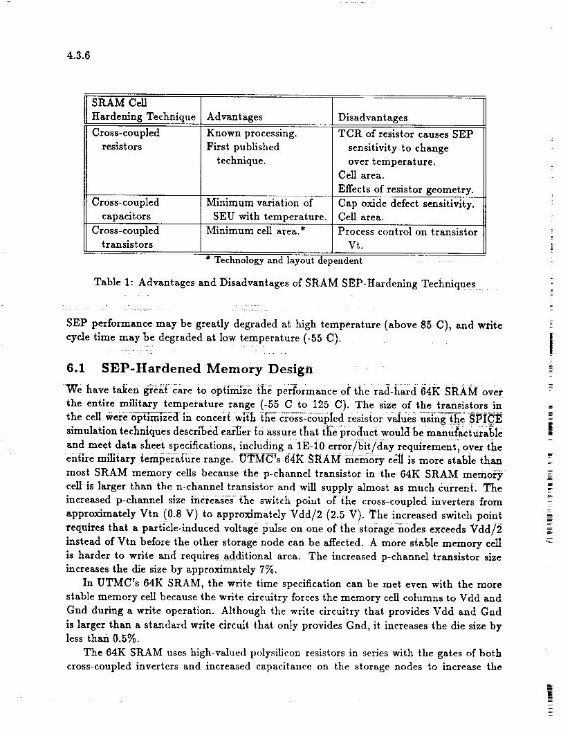
4.3.6
SRAM Cell
Hardening Technique
Cross-coupled
resistors
Cross-coupled
capacitors
Cross-coupled
transistors
Advantages
Known processing.
First published
technique.
Minimum variation of
SEU with temperature.
Minimum cellarea.*
* Technology and layout'de
Disadvantages
TCR of resistorcauses SEP
sensitivityto change
over temperature.
Cell area.
Effects of resistor geometry.
Cap oxide defect sensitivity.Cell area.
Process control on transistor
Vt.
)endent
Table 1: Advantages and Disadvantages of SRAM SEP-Hardening Techniques •
SEP performance may be greatly degraded at high temperature (above 85 C), and write
cycle time may be degraded at low temperature (-55 C).
6.1 SEP-YIardened Memory Design
We have taken great care to optimize the performance oi"the rad-hard 64K SRAM over
the entire military temperature range (-55 C to 125 C). The size of the transistors inthe cell Were optimized in concert with the cross-coupied resistor vaiues using the SPICEsimulation techniques descried earl_& to assure tI_at the product would bemanu_acturabIeand meet data sheet specifications, including a_lE-10 error/bit/day requirement-,-over theentire military temperature range. U'PMC's 64K SRAM memory c_ is more stabie than
most SRAM memory cells because the p-channel transistor in the 64K SRAM memorycelt is larger than the n-channel transistor and will supply almost as much current. Theincreased p-channe! slze increases _-he switch point oi_ the cross-coupled inverters from
approximately Vtn (0.8 V) to approximately Vdd/2 (_..5 V). The increased switch pointrequires that a particle-induced voltage pulse on one of the storagenodes exceeds Vdd/2instead of Vtn before the other storage node can be affected. A more stable memory ceilis harder to write and requires additional area. The increased p-channel transistor sizeincreases the die size by approximately 7%.
In UTMC's 64K SRAM, the write time specification can be met even with the morestable memory cell because the write circuitry forces the memory cell columns to Vdd andGrid during a write operation. Although the write circuitry that provides Vdd and Gnd
is larger than a standard write circuit that only provides Grid, it increases the die size byless than 0.5%.
The 64K SRAM uses high-valued polysilicon resistors in series with the gates of both
cross-coupled inverters and increased capacitance on the storage nodes to increase the
[
|f
E
_e
i
=

3rd NASA Symposium on VLSI Design 1991 4.3.7
feedback switching time. Increased stability and increased feedback switching time pro-
vide improved SEP protection. The 64K SRAM can use a lower valued resistor because
the memory cell is more stable than a typical SRAM. The lower valued resistor is more
manufacturable and is less affected by temperature. The polysilicon resistor process pro-
vides a tighter than typical control over the resistor value. This tight resistaxtee control
provides greater SEP protection over a wider temperature range and also allows shorter
write times. Including a resistor in the memory cell increases the die size by less than 9%.
The cross-coupled resistors are incorporated in the single layer of polysilicon which also
forms the gates of the transistors. Metal contacts for power and ground are incorporated
in every cell to help collect some of the charge deposited by a particle passing through a
nearby junction.
The effect of the cross-coupled resistors is to increase the threshold LET for SEP upset
and reduce the effective saturated cross-section of the device. [9] These effects for UTMC's
64K SRAM are shown in figure 5 and 6. Using the LET threshold and effective cross-section
from these graphs, the error rate in errors/bit/day as a function of resistor value may be
calculated for any space environment using CREME or SpaceRad as described above. The
error rate at 125 C (worst ease) for UTMC's 64K SRAM is shown in figure 7 as a function
of resistor value. By screening devices at the wafer level for resistor value and p-channel
drive current, we can guarantee an error rate of less than 1.0E-10 errors per bit per day at
125 C.
120
"_tl0E
_-_ 100
_0
_ 60v
_ 30
_ 20
_.1
_......._-
$ ............
Cocr Coeff = 0.9939
80 100 120 140 150 180
Resistor Volue (KOHMS)
........ Lineor Fit * DOIO
l.'_'r Thr,lshold (el, 125' C) vo'su$ Resisto¢ Volue (O 25' C)
200
_ 0.1
U_I
o.01
¢,.)
100 120 140 1£,0 18o 200
Resistor Value (KOHMS)
Figure 5: LET Threshold vs. Resistor
Value
Figure 6: Error Rate vs. Resistor Value
6.2 SEP-Hardened Flip-Flop Design
In logic systems, storage nodes such as flip-flops must retain data reliably, or the integrity
of the logic system can be severely compromised. A SEP-induced upset of a single bit in a
microprocessor register can send the system into an irrecoverable state. Detection of these
types of errors can require substantial overhead in software and hardware complexity and

4.3.8
tF O_
1E- 0'_
_'_ IE- 10
I
i_ 1E-.t"
_o IE- I2
o3_L
IE-I _,
IE- 14
%,
....=/_:_-..............___= _-!:'-_t-:!i:?!!-7ili11_::i:_;-iiz:::---:-
............i;i:,i:/IIL.:I£1.......... ..................................
IF- 15
80 90 100 I'I0 120 130 140
Resistor Vcflue (KOHMS)Uf)s_'ts per Bit-Boy (@ 125' C) ;eI'..u:_ F;'e_istor Voluo (_ 25' C in pocl, f].je)
Figure 7: Error Rate vs. Resistor Value
150
Clk
Nl
NCIk pl_--
_L P2
Q
Figure 8: Resistor Application in Flip-flop
is possible to substantially improve the SEP performance without introducing additional
processing complexity. However, there is usually a penalty in increased die area.
If the wafer fabrication process technology has poly-resistors available (used for SEP-
hardening SRAM cells described above), these resistors may be used to increase flip-flop
hardness as shown in figure 8. This technique can result in some performance clegradati6fi
of the flip-flop over temperature as reported by Sexton et al. [10] If resistors are not ave-
able, circuit techniques, coupled with the simulation techniques similar to those described
above, can be used to develop flip-flop register cells which have improved SEP performance
over conventional flip-flop circuits. [11,12]
To determine the effectiveness of the simulation technlques described =above, we Sim-
ulated the SEP upset for a number of the flip-flop cells in UTMC's gate-array library.
The simulations for one of these cells, DFAPCB - a D-type flip-flop whose logic diagram is
shown in figure 9, was compared with experimental data from heavy ion tests performed at
Brookhaven National Laboratory. To accurately determine the Upsetrate Of the flip'flop,
i
£
E
lE

3rd NASA Symposium on VLSI Design 1991 4.3.9
_:C:-_ $YV_C_
I
CL"C
X
x
X
f
j-
-k.
TRL;T_ -A 3.--
x' l _
x 0 0
_, 1 1 1
X I I O
3
CB
LOGIC DIAGRAM
CB CKB PB NANI32 '_v_
h" _,_NO_ I
O _ CK
CK8
CXB
CLK_CK
Figure 9: D-type Flip-flop Logic Diagram
it was necessary to determine the effective critical charge (the charge required to upset the
state of the flip-flop) for every node within the circuit for both a high-node state and a
low-node state. The effective critical charge, along with the junction area for each node,
was then used to determine the upset rate for the node using the SpaceRad program. The
sum of the upset rates for all nodes was then taken as the upset rate for the flip-flop. The
simulated error rate for the DFAPCB flip-flop was 4.24E-8 errors per cell per day. This
compares to an experimentally determined error rate of 3.38E-8 errors per cell per day for
this flip-flop cell.
We have also developed SEP-upset improved cells which support our radiation-hard
gate array cell library. Some of the cells are capable of providing an error rate of 1.0E-
l0 errors per cell per day. Fully redundant cells have also been designed which require
twice as many transistors as a non-redundant design, but are SEP-immune. The results of
this work have provided a number of guidelines for selecting and designing an SEP-hard
flip-flop. These guidelines are discussed in Table 2.
7 Conclusions
Use of the simulation techniques described in this paper substantially increases the con-
fidence that a design will meet its objectives for SEP hardness, and the cell layout can
be optimized without compromising circuit performance. We have demonstrated an SEP
error rate less than 1.0E-10 errors/bit-day for a 90% worst-case geosynchronous orbit en-
vironment over the entire -55 C to +125 C temperature range for a rad-hard 64K SRAM

4.3.!0
lffrobl_ Flip-Flop Design Approach
Minimize stacked
p-channel devices
Eliminate
transmission gates
Remove NOR gates and replace with NAND gates.
Remove transmission gates and replace with docked
inverters.
Minimize sensitive Simplify design as much as possible consistent with
node area functional requirements. Add redundant (parallel)
transistors on sensitive nodes internal to the cell.
Table 2: Design Considerations for Improving. SEP Hardness of Flip-Flops
while maintaining a less than 55 ns cycle time. We have also demonstrated the capability
to model the SEP error rate of gate array cells and have applied the simulation and design
techniques described in this paper to develop SEP-tolerant and SEP-hard flip-flop designs.
SEP hardness of integrated circuits cannot be assured by screening commercial devices,
or by normal system-level or logic-level design techniques. Good SEP hardness can only
be obtained by using a wafer fabrication process _ichprovides {he proper characteristics
and proper attention to good design practices _at_thetr ansistor level. Since commercial
semiconductor manufacturers do not consider SEP effects when designing their circuits,
it w_ Be necessary to develop custom circuits which are designed for SEP hardness _r
nnsslon-crlhcal appIicatmns.
8 Acknowledgmenta•o L ....
The authors would like to thank John Silver for providing valuable inputs to this paper.
References -
[11
[21
[3]
TMA DAVINCI is a trademark of Technology Modeling Associates, Inc._ . . . _ _ ........ - . _ -_ :: = .... : _
J. J.-Sffver/]2ircuit Designs for Relia-bie Ol_eration in Iiazardous Environments,
N3REC Tutorial Short Course, July 1987 an_-re-fereixces therein. - " -
A. Knudson, A. Campbell, Comparison of Experimental Charge Collection Waveforms
with PISCES Calcuia.tiOns, IEEETrans Nucl Sci.' NS-38' i-_i_ _:_ .... =/7_ -
[4] J. Rollins et al., Cost-Effective Numerical Simulation of SEU, IBEE Trans Nucl ,qci.,
NS-35, 1988.
[5] J. H. Adams Jr:,R. Silberberg, and C. H. Tsao, Cosmic Ray Effects on _Mi_cro_elee-
tronics, NRL Memorandum Report H506, Naval Research Laboratory, Washington,
D.C.
=

3rd NASA Symposium on VLSI Design 1991 4.3.11
[6]
[7]
Is]
[9]
[10]
[11]
[12]
SpaceRad is a product of Space Radbrtion, Severn Communications Corp.
S. E. DieM, et al., Error Analysis and Prevention of Cosmic Ion-Induced Soft Errors
in Static CMOS RAMs, IEEE Trans on Nucl Sci, Vol. NS-29, December 1982, page
2032.
L. AUes, K.L. Jones, :I.E. Clark, S.C. Lee, W.F. Kraus, S.E. Kerns, L.W. Massengil,
Rad-Hard SOI/SRAM Design Using a Predictive SEU Device Model, Digest of Papers,
GOMAC, Vol. 16, 1990, page 443.
J.R. Adams, M. Barry, J. Silver, and P. Rudeck, Design, Simulation, and Evaluation
of a SEP-hard SRAM Memory Cell, RADEGS, August 1991.
F.W. Sexton, et al., SEU Simulation and Testing of Resistor-Hardened D-Latches in
the SA-3300 Microprocessor NSREC, July 1991, to be published in IEEE Trans Nucl
5ci., 1991, and references therein.
S. E. Diehl, J. E. Vinson, B.D. Sharer, and T. M. Mnich, Considerations for Single
Event Immune VLSI Logic, IEEE Trans on Nucl Sci., Vol. NS-30, December 1983.
L.R. Rockett, Jr., An SEU-Hardened CMOS Data Latch Design, IEEE Trans Nucl
Sci., Vol. 35, No. 6, December, 1988.
