nanoparticle fabrication by geometrically confined nanosphere lithography
TRANSCRIPT

Nanoparticle fabrication bygeometrically confined nanospherelithography
Ryan C. DenommeKrishna IyerMichael KrederBrendan SmithPatricia M. Nieva
Downloaded From: http://nanolithography.spiedigitallibrary.org/ on 09/06/2013 Terms of Use: http://spiedl.org/terms
Nanoparticle fabrication by geometrically confinednanosphere lithography
Ryan C. DenommeKrishna IyerMichael KrederBrendan SmithPatricia M. NievaUniversity of WaterlooSensors and Integrated Microsystems LaboratoryMechanical Engineering200 University Avenue WestWaterloo, Ontario N2L 3G1, CanadaE-mail: [email protected]
Abstract. Arrays of metal nanoparticles, typically gold or silver, exhibitlocalized surface plasmon resonance, a phenomenon that has manyapplications, such as chemical and biological sensing. However, fabrica-tion of metal nanoparticle arrays with high uniformity and repeatability, at areasonable cost, is difficult. Nanosphere lithography (NSL) has been usedbefore to produce inexpensive nanoparticle arrays through the use ofmonolayers of self-assembled microspheres as a deposition mask.However, control over the size and location of the arrays, as well as uni-formity over large areas is poor, thus limiting its use to research purposes.In this paper, a new NSL method, called here geometrically confined NSL(GCNSL), is presented. In GCNSL, microsphere assembly is confined togeometric patterns defined in photoresist, allowing high-precision andlarge-scale nanoparticle patterning while still remaining low cost. Usingthis newmethod, it is demonstrated that 400 nm polystyrene microspherescan be assembled inside of large arrays of photoresist patterns. Resultsshow that optimal microsphere assembly is achieved with long and narrowrectangular photoresist patterns. The combination of microsphere mono-layers and photoresist patterns is then used as a deposition mask toproduce silver nanoparticles at precise locations on the substrate withhigh uniformity, repeatability, and quality. © 2013 Society of Photo-OpticalInstrumentation Engineers (SPIE) [DOI: 10.1117/1.JMM.12.3.031106]
Subject terms: plasmonics; nanosphere lithography; nanoparticles; biosensors;nanofabrication; microfabrication; self-assembly.
Paper 13049SSP received Apr. 11, 2013; revised manuscript received Jun. 21,2013; accepted for publication Jul. 1, 2013; published online Jul. 26, 2013.
1 IntroductionMetal nanoparticles (NPs), mainly gold and silver, havereceived widespread attention in recent years1–3 in partdue to the optical phenomenon they exhibit, known as local-ized surface plasmon resonance (LSPR). LSPR is caused bythe coherent oscillation of the material’s surface conductionelectrons, which leads to a large absorbance peak in the ultra-violet (UV), visible, or near infrared range.4 The applicationsutilizing this effect are widespread, including chemical sen-sors,5 biological sensors,6 surface-enhanced Raman spectros-copy,7 solar cells,8 and light-emitting diodes.9 Using metalNPs for the development of molecular biosensors is a par-ticularly interesting application, as it is a label-free techniquewith limits of detection that can reach the pico to nanomolarrange.6,10–13 In biosensor applications, binding of moleculesto the surface of the metal NPs causes a large shift in theLSPR peak position, since the position is extremely sensitiveto the local dielectric properties of the particles.14 The highsensitivity, simplicity, and low cost of LSPR sensors makethem suitable for point-of-care diagnostics or other lab-on-a-chip sensor applications.15
Metal NP arrays used in LSPR sensors must be uniform insize, shape, and composition, and should have an economicaland repeatable fabrication method.14 However, the cost andpracticality of existing fabrication methods of metal NParrays are major hurdles in bringing LSPR-based sensors tothe market.16 Among these methods, electron-beam lithography
(EBL) and nanoimprint lithography (NIL) offer high resolu-tion, uniformity, and repeatability for array fabrication, butare costly. On the other hand, a simple and inexpensive tech-nique that is used often to produce LSPR substrates forresearch is nanosphere lithography (NSL).17 In NSL, amonolayer (ML) of hexagonal close-packed (HCP) polysty-rene (PS) microspheres is formed on a substrate through aself-assembly process that is induced by the evaporationof liquid from a colloidal solution [Fig. 1(a)]. A thin layer ofmetal is then deposited, with the HCP microsphere layer act-ing as a mask. Deposition of metal through the interstitialsites of the HCP microsphere layer produces NPs of triangu-lar shape on the substrate, followed by the removal of micro-sphere layer [Fig. 1(b)].18 The size of the microspheresdetermines the size of the NPs. For instance, when using400 nm diameter spheres, the length of the perpendicularbisector of the nanotriangles formed is on the order of100 nm.19
In general, NSL lacks the uniformity, reproducibility, andcontrol for it to be used for the production of practical LSPRsensors requiring localized arrays of uniform size. This ismainly due to the random formation of sub-ML (SML)and double layer (DL) regions.20 Typically, the ML is formedby drop coating and many variations have been investigatedto increase control and uniformity.21 One method is throughconvective self-assembly (CSA) NSL (CSANSL),20,22,23 inwhich a drop of microsphere solution is trapped between aspreader and a substrate. The substrate is mechanicallymoved and the ML grows from the three-phase contact lineof the meniscus as it is dragged across the substrate surface.0091-3286/2013/$25.00 © 2013 SPIE
J. Micro/Nanolith. MEMS MOEMS 031106-1 Jul–Sep 2013/Vol. 12(3)
J. Micro/Nanolith. MEMS MOEMS 12(3), 031106 (Jul–Sep 2013)
Downloaded From: http://nanolithography.spiedigitallibrary.org/ on 09/06/2013 Terms of Use: http://spiedl.org/terms

CSANSL has shown to produce large, uniform ML regions,the location of which is controlled by the spreader position.However, there is still a large amount of area within thespreader region that is not usable, and the exact location ofthe NP arrays cannot be controlled. Control over the arraylocation is important for devices that require multiple masksand processing steps, such as sensors with integrated micro-fluidics and optics, as well as multiplexed sensors. Ideally,one could pattern the NPs in a way similar to typical photo-lithographic patterning, with a set number and size of uniquesensor areas in an array at defined locations on the substrate.To accomplish this level of control with self-assemblytechniques such as NSL, chemical24 and physical,23,25–29
templates have been used to fix the location of the nano/microsphere assemblies. Although some success has beenachieved in assembling microspheres in predetermined loca-tions, these MLs have not been used to produce NP arrays.
In this paper, an improved NSL process, which we havecalled geometrically confined NSL (GCNSL),30 is reported.In GCNSL, traditional photolithography is combined withthe CSANSL process. The microspheres are spread overmicron scale patterns made in photoresist. Due to the geo-metrical confinement of the photoresist patterns, the micro-spheres preferentially assemble into these patterns in HCPMLs. After metal deposition and upon removal of the photo-resist and microspheres, patterned arrays of NPs remain.GCNSL allows for the low-cost fabrication of NPs that ischaracteristic of NSL, but with the patterning quality andcontrol of traditional UV photolithography. This allows NPsto be patterned in exact, predefined locations on the substrateaccording to the desired mask layout, but for a fraction of thecost of using techniques such as EBL or NIL.
Here, the results of NP fabrication via both CSANSL onglass and GCNSL on glass-photoresist substrates are pre-sented and compared. Various pattern geometries, such assquares and rectangles of different sizes, are used to inves-tigate the effects of geometry on the ML assembly inGCNSL. The effects of spreading speed, temperature, andhumidity on the different NSL processes are also discussed.
2 Methodology and Materials
2.1 Substrate Cleaning and Photolithography
Glass wafers (EAGLE2000, Precision Glass and Optics,Santa Ana) 3-in diameter and 1.1 mm thick, were used asthe substrates. Wafers were washed in deionized (DI) water,followed by ultrasonic cleaning in acetone for 10 min, and inisopropanol for 10 min more. Samples were blown dry with
nitrogen, and cleaned for 10 min in a UV-ozone cleaner torender the surface highly hydrophilic and remove anyorganic residue.
For GCNSL, a chrome photomask was designed withvarious geometrical structures, including arrays of squares,rectangles, and parallelograms of various sizes. Followingcleaning, substrates were dehydration baked at 120°C for1 min. Hexamethyldisilazane primer was pipetted onto thewafer, and spun at 4000 RPM for 1 min. Next, 5 mL ofAZ3312 photoresist (AZ Electronic Materials,Branchburg) was added to 2.5 mL of propylene glycolmonomethyl ether acetate (PGMEA, Sigma Aldrich, St.Louis) for a dilution to 67% v∕v. This was done to producea 400 nm thick resist, which is outside of the normal thick-ness range of the AZ3312. The resist was spun at 4000 RPMfor 1 min, and baked at 90°C for 1 min. Resist thickness wasverified with a Dektak 8 Stylus Profilometer. The wafersand mask were loaded into a mask aligner (MA6, SUSSMicroTec, Sunnyvale) and exposed to 365 nm UV lightfor 2.8 to 3.1 s while in vacuum contact. The wafers wereplaced in a beaker of AZ300 MIF developer (AZElectronic Materials) for 30 s, and then placed into a beakerof DI water for rinsing prior to nitrogen blow drying. Finally,the samples were post-baked at 90°C for 1 min and inspectedunder an optical microscope. This process creates 400 nmdeep wells within the photoresist in the patterns definedby the photomask.
2.2 NSL: Microsphere Assembly, Metal Deposition,and Lift-Off
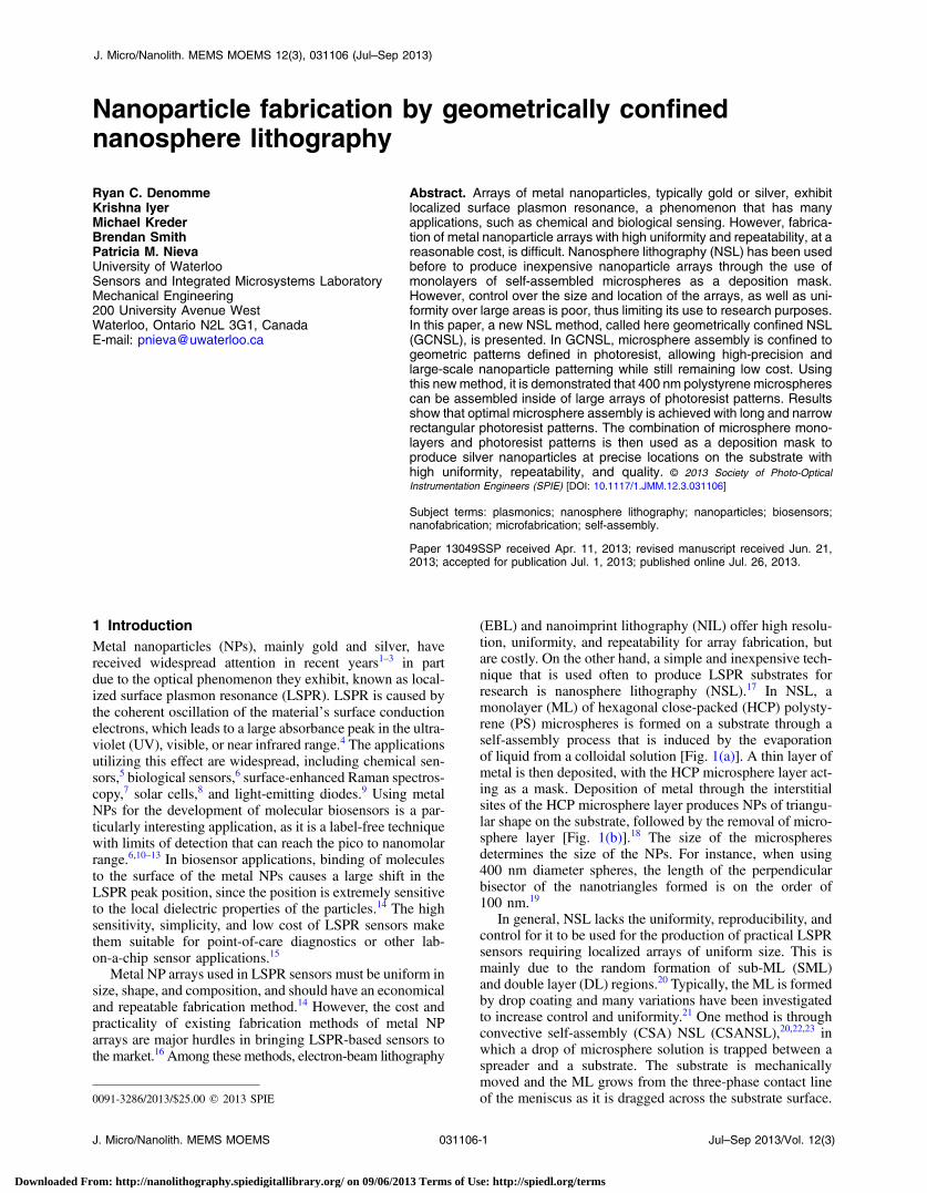
The NSL fabrication tool used in this paper is shown inFig. 2. The same setup was used for both the CSANSLand GCNSL processes. The setup consisted of a manualXY-R stage (Thorlabs Inc., Newton) for positioning thewafer under the spreader. The spreader was made of aglass cover slip approximately 4-mm wide, and was attachedto a z-stage (Thorlabs Inc., Newton) with an adjustable angleto control the spreader height and contact angle. The temper-ature of the wafer was controlled using a Peltier stage (Digi-Key Corp., Thief River Falls) set to 25°C� 0.1°C. A fan andheat sink were used to improve the temperature stability ofthe stage. Finally, a motorized stage (Zaber TechnologiesInc., Vancouver, Canada) was used to move the substrateunder the spreader at a well-controlled velocity.
The fabrication process flow for both the CSANSL andthe GCNSL processes are shown in Fig. 3. PS microspheres,400 nm diameter and carboxyl functionalized (4% w∕v),were purchased from Invitrogen Corp., Carlsbad and used
Fig. 1 Illustration of the NSL fabrication method. (a) Render of the HCPmicrosphere ML that is used as a deposition mask, and (b) render of the NParray that results after metal deposition and removal of the microsphere mask.
J. Micro/Nanolith. MEMS MOEMS 031106-2 Jul–Sep 2013/Vol. 12(3)
Denomme et al.: Nanoparticle fabrication by geometrically confined nanosphere lithography
Downloaded From: http://nanolithography.spiedigitallibrary.org/ on 09/06/2013 Terms of Use: http://spiedl.org/terms
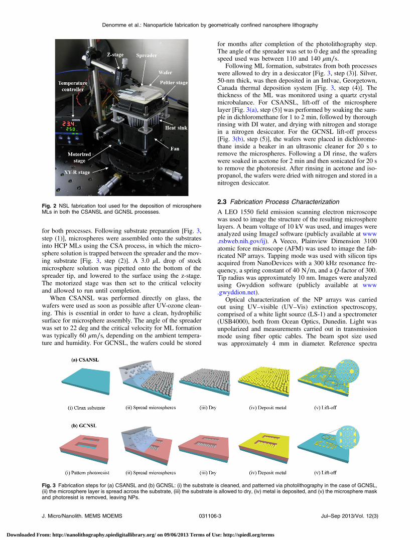
for both processes. Following substrate preparation [Fig. 3,step (1)], microspheres were assembled onto the substratesinto HCP MLs using the CSA process, in which the micro-sphere solution is trapped between the spreader and the mov-ing substrate [Fig. 3, step (2)]. A 3.0 μL drop of stockmicrosphere solution was pipetted onto the bottom of thespreader tip, and lowered to the surface using the z-stage.The motorized stage was then set to the critical velocityand allowed to run until completion.
When CSANSL was performed directly on glass, thewafers were used as soon as possible after UV-ozone clean-ing. This is essential in order to have a clean, hydrophilicsurface for microsphere assembly. The angle of the spreaderwas set to 22 deg and the critical velocity for ML formationwas typically 60 μm∕s, depending on the ambient tempera-ture and humidity. For GCNSL, the wafers could be stored
for months after completion of the photolithography step.The angle of the spreader was set to 0 deg and the spreadingspeed used was between 110 and 140 μm∕s.
Following ML formation, substrates from both processeswere allowed to dry in a desiccator [Fig. 3, step (3)]. Silver,50-nm thick, was then deposited in an Intlvac, Georgetown,Canada thermal deposition system [Fig. 3, step (4)]. Thethickness of the ML was monitored using a quartz crystalmicrobalance. For CSANSL, lift-off of the microspherelayer [Fig. 3(a), step (5)] was performed by soaking the sam-ple in dichloromethane for 1 to 2 min, followed by thoroughrinsing with DI water, and drying with nitrogen and storagein a nitrogen desiccator. For the GCNSL lift-off process[Fig. 3(b), step (5)], the wafers were placed in dichlorome-thane inside a beaker in an ultrasonic cleaner for 20 s toremove the microspheres. Following a DI rinse, the waferswere soaked in acetone for 2 min and then sonicated for 20 sto remove the photoresist. After rinsing in acetone and iso-propanol, the wafers were dried with nitrogen and stored in anitrogen desiccator.
2.3 Fabrication Process Characterization
A LEO 1550 field emission scanning electron microscopewas used to image the structure of the resulting microspherelayers. A beam voltage of 10 kV was used, and images wereanalyzed using ImageJ software (publicly available at www.rsbweb.nih.gov/ij). A Veeco, Plainview Dimension 3100atomic force microscope (AFM) was used to image the fab-ricated NP arrays. Tapping mode was used with silicon tipsacquired from NanoDevices with a 300 kHz resonance fre-quency, a spring constant of 40 N∕m, and a Q-factor of 300.Tip radius was approximately 10 nm. Images were analyzedusing Gwyddion software (publicly available at www.gwyddion.net).
Optical characterization of the NP arrays was carriedout using UV–visible (UV–Vis) extinction spectroscopy,comprised of a white light source (LS-1) and a spectrometer(USB4000), both from Ocean Optics, Dunedin. Light wasunpolarized and measurements carried out in transmissionmode using fiber optic cables. The beam spot size usedwas approximately 4 mm in diameter. Reference spectra
Fig. 2 NSL fabrication tool used for the deposition of microsphereMLs in both the CSANSL and GCNSL processes.
Fig. 3 Fabrication steps for (a) CSANSL and (b) GCNSL: (i) the substrate is cleaned, and patterned via photolithography in the case of GCNSL,(ii) the microsphere layer is spread across the substrate, (iii) the substrate is allowed to dry, (iv) metal is deposited, and (v) the microsphere maskand photoresist is removed, leaving NPs.
J. Micro/Nanolith. MEMS MOEMS 031106-3 Jul–Sep 2013/Vol. 12(3)
Denomme et al.: Nanoparticle fabrication by geometrically confined nanosphere lithography
Downloaded From: http://nanolithography.spiedigitallibrary.org/ on 09/06/2013 Terms of Use: http://spiedl.org/terms
were taken in air. A personal computer with SpectraSuite soft-ware (Ocean Optics) was used to acquire data. Data process-ing was done in MATLAB® software.
3 Results and Discussion
3.1 CSANSL on Glass
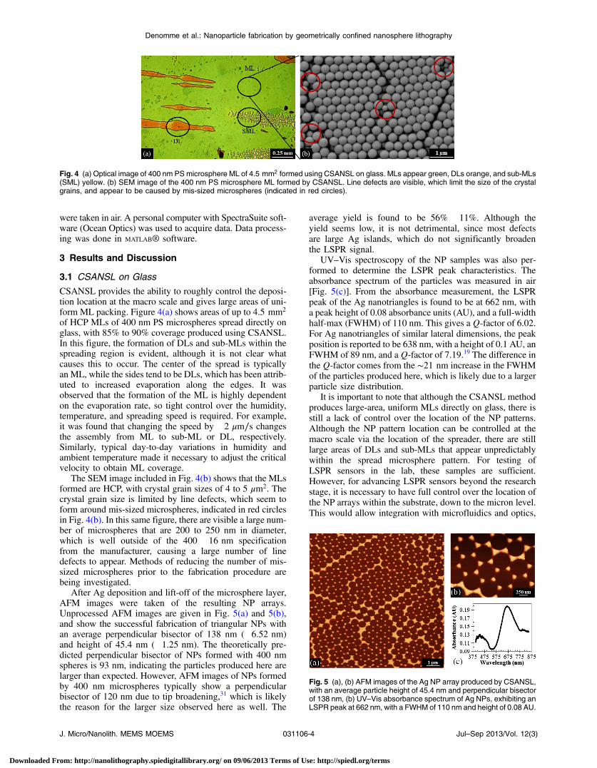
CSANSL provides the ability to roughly control the deposi-tion location at the macro scale and gives large areas of uni-form ML packing. Figure 4(a) shows areas of up to 4.5 mm2
of HCP MLs of 400 nm PS microspheres spread directly onglass, with 85% to 90% coverage produced using CSANSL.In this figure, the formation of DLs and sub-MLs within thespreading region is evident, although it is not clear whatcauses this to occur. The center of the spread is typicallyan ML, while the sides tend to be DLs, which has been attrib-uted to increased evaporation along the edges. It wasobserved that the formation of the ML is highly dependenton the evaporation rate, so tight control over the humidity,temperature, and spreading speed is required. For example,it was found that changing the speed by �2 μm∕s changesthe assembly from ML to sub-ML or DL, respectively.Similarly, typical day-to-day variations in humidity andambient temperature made it necessary to adjust the criticalvelocity to obtain ML coverage.
The SEM image included in Fig. 4(b) shows that the MLsformed are HCP, with crystal grain sizes of 4 to 5 μm2. Thecrystal grain size is limited by line defects, which seem toform around mis-sized microspheres, indicated in red circlesin Fig. 4(b). In this same figure, there are visible a large num-ber of microspheres that are 200 to 250 nm in diameter,which is well outside of the 400� 16 nm specificationfrom the manufacturer, causing a large number of linedefects to appear. Methods of reducing the number of mis-sized microspheres prior to the fabrication procedure arebeing investigated.
After Ag deposition and lift-off of the microsphere layer,AFM images were taken of the resulting NP arrays.Unprocessed AFM images are given in Fig. 5(a) and 5(b),and show the successful fabrication of triangular NPs withan average perpendicular bisector of 138 nm (�6.52 nm)and height of 45.4 nm (�1.25 nm). The theoretically pre-dicted perpendicular bisector of NPs formed with 400 nmspheres is 93 nm, indicating the particles produced here arelarger than expected. However, AFM images of NPs formedby 400 nm microspheres typically show a perpendicularbisector of 120 nm due to tip broadening,31 which is likelythe reason for the larger size observed here as well. The
average yield is found to be 56%� 11%. Although theyield seems low, it is not detrimental, since most defectsare large Ag islands, which do not significantly broadenthe LSPR signal.
UV–Vis spectroscopy of the NP samples was also per-formed to determine the LSPR peak characteristics. Theabsorbance spectrum of the particles was measured in air[Fig. 5(c)]. From the absorbance measurement, the LSPRpeak of the Ag nanotriangles is found to be at 662 nm, witha peak height of 0.08 absorbance units (AU), and a full-widthhalf-max (FWHM) of 110 nm. This gives a Q-factor of 6.02.For Ag nanotriangles of similar lateral dimensions, the peakposition is reported to be 638 nm, with a height of 0.1 AU, anFWHM of 89 nm, and aQ-factor of 7.19.19 The difference inthe Q-factor comes from the ∼21 nm increase in the FWHMof the particles produced here, which is likely due to a largerparticle size distribution.
It is important to note that although the CSANSL methodproduces large-area, uniform MLs directly on glass, there isstill a lack of control over the location of the NP patterns.Although the NP pattern location can be controlled at themacro scale via the location of the spreader, there are stilllarge areas of DLs and sub-MLs that appear unpredictablywithin the spread microsphere pattern. For testing ofLSPR sensors in the lab, these samples are sufficient.However, for advancing LSPR sensors beyond the researchstage, it is necessary to have full control over the location ofthe NP arrays within the substrate, down to the micron level.This would allow integration with microfluidics and optics,
Fig. 4 (a) Optical image of 400 nm PS microsphere ML of 4.5 mm2 formed using CSANSL on glass. MLs appear green, DLs orange, and sub-MLs(SML) yellow. (b) SEM image of the 400 nm PS microsphere ML formed by CSANSL. Line defects are visible, which limit the size of the crystalgrains, and appear to be caused by mis-sized microspheres (indicated in red circles).
Fig. 5 (a), (b) AFM images of the Ag NP array produced by CSANSL,with an average particle height of 45.4 nm and perpendicular bisectorof 138 nm, (b) UV–Vis absorbance spectrum of Ag NPs, exhibiting anLSPR peak at 662 nm, with a FWHM of 110 nm and height of 0.08 AU.
J. Micro/Nanolith. MEMS MOEMS 031106-4 Jul–Sep 2013/Vol. 12(3)
Denomme et al.: Nanoparticle fabrication by geometrically confined nanosphere lithography
Downloaded From: http://nanolithography.spiedigitallibrary.org/ on 09/06/2013 Terms of Use: http://spiedl.org/terms

designing of highly multiplexed sensor arrays, and a morerepeatable sensor response. The GCNSL process was devel-oped to address these issues.
3.2 GCNSL on Glass Photoresist
The newly developed GCNSL method allows full controlover the location of the NP arrays through the use ofphotolithographically generated patterns. For this work, thephotoresist was processed to form 400 nm deep wells (seeSec. 2.1), with patterns of varying size and shape.Assembly of the microsphere ML within the defined tem-plates results in NP arrays that are patterned via photolithog-raphy. By using the patterned photoresist layer, anymicrosphere deposition that occurs outside of the definedpatterns is removed in the lift-off procedure.
In initial attempts, it was difficult to form uniform MLswithin the defined patterns using the fabrication parametersof CSANSL. This was mainly for two reasons: (1) anydefects that occurred outside of the patterns often continueto occur into the patterns because the crystal growth propa-gates, and (2) if ordered ML deposition occurred on the
resist, it was very difficult to achieve ML deposition withinthe patterns; usually, double or triple layers resulted withinthe patterns. To circumvent these problems, experimentswere performed at increased spreading speeds, in the 110 to140 μm∕s range. During these experiments, it was observedthat HCP MLs begin to form on the resist surface at speedsbelow 110 μm∕s, and the problems noted above occur. Onthe other hand, when the speed is above 110 μm∕s, micro-sphere deposition on the resist is randomly distributed asopposed to being close-packed. In this case, the micro-spheres assemble into uniform HCP MLs inside of the pat-terns, and defects that occur on the photoresist are not able topropagate into the wells. Therefore, it was found that byspreading at speeds higher than 110 μm∕s over the photore-sist patterns, microspheres preferentially assemble into high-quality HCP MLs inside of the resist patterns.
Observations under SEM also showed that the degree towhich the patterns are filled is highly dependent on the sizeand shape of the patterns. For instance, it was very difficult toform quality microsphere ML within arrays of squares orparallelograms with side lengths from 2 to 20 μm. Withinthis range, patterns with lengths below 6 μm in size were
Fig. 6 SEM image of (a) a 6 × 6 μm square photoresist well completely filled with microspheres but exhibiting a large number of defects, and (b) a20 × 20 μm photoresist well that is only partially filled with microspheres.
Fig. 7 SEM images of microsphere assembly inside of 20 μm long patterns for widths of (a) 4 μm, (b) 8 μm, and (c) 14 μm. As the width is increased,the coverage of the microsphere ML decreases. Poor coverage is seen for widths larger than 6 μm. Patterns were filled right to left. At the leadingedge (the right edge in the images), the formation of a buffer zone in which no microspheres assemble can be seen.
J. Micro/Nanolith. MEMS MOEMS 031106-5 Jul–Sep 2013/Vol. 12(3)
Denomme et al.: Nanoparticle fabrication by geometrically confined nanosphere lithography
Downloaded From: http://nanolithography.spiedigitallibrary.org/ on 09/06/2013 Terms of Use: http://spiedl.org/terms
typically filled [Fig. 6(a)], while those larger than 6 μm couldonly be partially filled [Fig. 6(b)]. However, using patternssmaller than 6 μm is not practical, as edge and cornerinduced defects dominated the ML, greatly reducing thequality of the NP arrays produced. Therefore, squares andparallelograms were not considered as viable patterns forcontrolling the microsphere assembly, although with furtherprocess optimization of the process this may be possible.
When rectangular patterns with the long axis parallel tothe spreading direction were used, improved microsphereassembly in the patterns was observed when compared tothe square patterns. The arrays of rectangles of 4, 6, 8,10, 14, 20, 30, and 40 μm in width and 20, 100, and
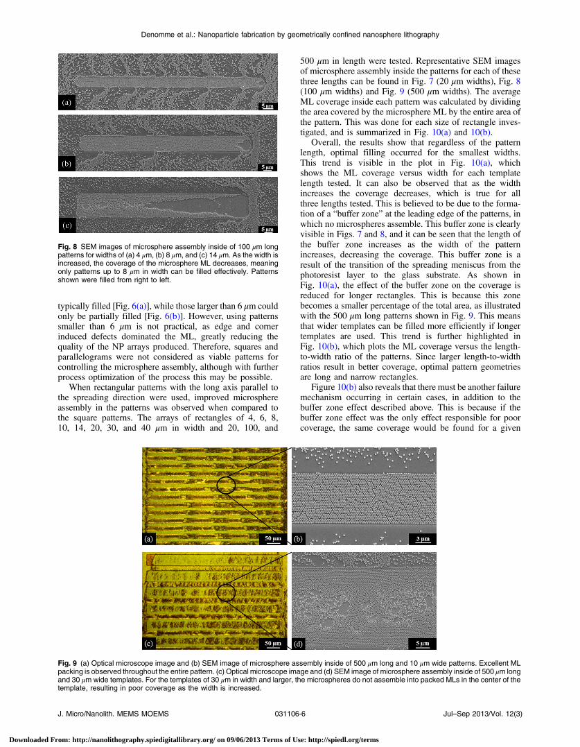
500 μm in length were tested. Representative SEM imagesof microsphere assembly inside the patterns for each of thesethree lengths can be found in Fig. 7 (20 μm widths), Fig. 8(100 μm widths) and Fig. 9 (500 μm widths). The averageML coverage inside each pattern was calculated by dividingthe area covered by the microsphere ML by the entire area ofthe pattern. This was done for each size of rectangle inves-tigated, and is summarized in Fig. 10(a) and 10(b).
Overall, the results show that regardless of the patternlength, optimal filling occurred for the smallest widths.This trend is visible in the plot in Fig. 10(a), whichshows the ML coverage versus width for each templatelength tested. It can also be observed that as the widthincreases the coverage decreases, which is true for allthree lengths tested. This is believed to be due to the forma-tion of a “buffer zone” at the leading edge of the patterns, inwhich no microspheres assemble. This buffer zone is clearlyvisible in Figs. 7 and 8, and it can be seen that the length ofthe buffer zone increases as the width of the patternincreases, decreasing the coverage. This buffer zone is aresult of the transition of the spreading meniscus from thephotoresist layer to the glass substrate. As shown inFig. 10(a), the effect of the buffer zone on the coverage isreduced for longer rectangles. This is because this zonebecomes a smaller percentage of the total area, as illustratedwith the 500 μm long patterns shown in Fig. 9. This meansthat wider templates can be filled more efficiently if longertemplates are used. This trend is further highlighted inFig. 10(b), which plots the ML coverage versus the length-to-width ratio of the patterns. Since larger length-to-widthratios result in better coverage, optimal pattern geometriesare long and narrow rectangles.
Figure 10(b) also reveals that there must be another failuremechanism occurring in certain cases, in addition to thebuffer zone effect described above. This is because if thebuffer zone effect was the only effect responsible for poorcoverage, the same coverage would be found for a given
Fig. 8 SEM images of microsphere assembly inside of 100 μm longpatterns for widths of (a) 4 μm, (b) 8 μm, and (c) 14 μm. As the width isincreased, the coverage of the microsphere ML decreases, meaningonly patterns up to 8 μm in width can be filled effectively. Patternsshown were filled from right to left.
Fig. 9 (a) Optical microscope image and (b) SEM image of microsphere assembly inside of 500 μm long and 10 μm wide patterns. Excellent MLpacking is observed throughout the entire pattern. (c) Optical microscope image and (d) SEM image of microsphere assembly inside of 500 μm longand 30 μm wide templates. For the templates of 30 μm in width and larger, the microspheres do not assemble into packed MLs in the center of thetemplate, resulting in poor coverage as the width is increased.
J. Micro/Nanolith. MEMS MOEMS 031106-6 Jul–Sep 2013/Vol. 12(3)
Denomme et al.: Nanoparticle fabrication by geometrically confined nanosphere lithography
Downloaded From: http://nanolithography.spiedigitallibrary.org/ on 09/06/2013 Terms of Use: http://spiedl.org/terms

length-to-width ratio. However, from Fig. 10(b), it is clearthat patterns of the same length-to-width ratio do not resultin the same coverage. This is evident specifically for lengthsof 100 and 500 μm at length-to-width ratios below 25. To thisregard, SEM images [Fig. 9(b)] show that for widths of 30and 40 μm, sub-ML coverage occurs within the center ofthe template, while ML coverage occurs at the edges. Thisis very different from the buffer zone effect as this occursthroughout the entire length of the template as oppose tojust the leading edge. Although spreading at a slower speedmight allow complete filling of these larger widths, the speedcannot be reduced below 110 μm∕s or ML assembly willoccur on the resist surface, making the deposition much moredifficult to control. Therefore, there may be an upper limit onthe width of template that can be used, regardless of howlong the template is made. In this study, using templatesof 500 μm in length, templates with widths from 4 to20 μm could be filled with close to 100% coverage. The uni-formity and quality of the ML packing throughout thetemplate arrays was found to be very high, as is evidentfrom the optical microscope images in Fig. 9(a). The qualityis maintained almost throughout the entire area of the
pattern, and packing quality between patterns is consistent.This is true for all of the patterns tested.
After Ag deposition and lift-off of the photoresist andmicrospheres, the NP samples were analyzed with AFMand UV–Vis spectroscopy and compared to the resultsobtained from CSANSL. A comparison of the characteristicsof the NPs produced from each technique is given in Table 1.AFM of the particles produced by GCNSL in 10 × 500 μm2
rectangle patterns [Fig. 11(a) and 11(b)] confirms that NPsonly exist inside of the patterns defined by the photoresist.From unprocessed AFM images of the 10 × 500 μm2 rectan-gle patterns, the NPs have an average height of 44.0 nm(�3.47 nm) and average perpendicular bisector of 115 nm(�9.31 nm), which is smaller than the NPs produced byGCNSL. This may indicate more compact packing of themicrospheres in the GCNSL process, but could also be dueto difference in AFM tip quality. The average yield of theGCNSL fabrication process was found to be 52% (�2.6%),which is comparable to the yield from CSANSL, indicatingthat the number of defects is not significantly affected usingthe GCNSL process. The GCNSL fabricated NP arrays retainthe large-scale uniformity observed prior to lift-off, as shownin the post-lift-off microscope image in Fig. 12.
UV–Vis characterization of the 500 μm long templatesconfirms that the NPs formed using GCNSL exhibit theLSPR phenomenon [Fig. 11(c)]. The LSPR peak is found
Fig. 10 (a) Plot of the ML coverage versus the width of the template for each length tested showing that optimal coverage occurs at the narrowestwidths, and that longer templates allow for high coverage to be achieved for larger widths, and (b) plot of the ML coverage versus the length-to-widthratio of the rectangular templates tested, further indicating that long and narrow templates result in optimal coverage. Error bars indicate onestandard deviation above and below the average, taken from three independent measurements.
Table 1 Comparison of Ag NP characteristics produced by CSANSLand GCNSL.
CSANSL GCNSL
Heighta (nm) 45.4 44.0
P. Bisectora (nm) 138 115
Yield (%) 56 52
Peak position (nm) 662 619
Peak height (AU) 0.08 0.03
FWHM (nm) 110 100
Q-factor 6.02 6.2
Cost ($∕mm2) 0.03 0.06
aMeasured from unprocessed AFM images.
Fig. 11 (a and b) AFM images of the Ag NP array produced byGCNSL using 10 μm × 500 μm templates, (c) UV–Vis absorbancespectrum of Ag NPs produced by GCNSL, exhibiting an LSPRpeak at 619 nm, with an FWHM of 100 nm and height of 0.03 AU.
J. Micro/Nanolith. MEMS MOEMS 031106-7 Jul–Sep 2013/Vol. 12(3)
Denomme et al.: Nanoparticle fabrication by geometrically confined nanosphere lithography
Downloaded From: http://nanolithography.spiedigitallibrary.org/ on 09/06/2013 Terms of Use: http://spiedl.org/terms

to be at 619 nm, with a peak height of 0.03 AU and FWHMof 100 nm. This gives a Q-factor of 6.20, which is very closeto the Q-factor of the CSANSL samples, indicating similarLSPR peak quality. Compared to the LSPR peak from theCSANSL sample, the peak is red shifted by 43 nm,which is likely due to the smaller average particle size.32 Thepeak height is also lower in the GCNSL sample, which is dueto a lower overall density of particles in the GCNSL sampledue to the spacing of the rectangular patterns and a smalleroverall pattern size (0.25 μm2 compared with 4 to 5 mm2).The FWHM of the GCNSL peak is improved by 10 nm com-pared to the CSANSL sample, which might indicate higherlarge-scale uniformity amongst the NPs produced with thistechnique.
Overall, the GCNSL process is able to produce NPswithin predefined templates made using photoresist, whichis a major advantage and improvement over previous meth-ods. However, it also offers other advantages. The spreadingspeed can be anywhere from 110 to 135 μm∕s and MLassembly still occurs within the templates, which means theprocess is less dependent on temperature and humidity fluc-tuations. Compared to CSANSL, this makes GCNSL morerobust and repeatable. GCNSL also produced more uniformNPs, with fewer large-scale defects, as any defects that occuron the photoresist are removed in the lift-off process, anddefects are not able to propagate over large distances. It isestimated that the cost of producing NPs with GCNSL is0.06∕mm2, assuming the use of 3 in wafers and using typicallab equipment fee rates and processing times. Similarly, thecost for CSANSL is estimated to be 0.03∕mm2. Therefore,although GCNSL is twice the cost due to the photolithogra-phy steps involved, it is believed that its benefits are wellworth the cost increase. For instance, the cost of GCNSLis still extremely low compared to EBL, which is estimatedto be at 250∕mm2, over 4000 times more expensive.
4 ConclusionsMetal NP arrays suitable for LSPR sensor applications weresuccessfully fabricated using both CSANSL and a newlydeveloped GCNSL technique. CSANSL was capable ofproducing large areas of NP arrays on a substrate, but hadlimited control over the array size and location. The silverNPs produced by CSANSL were 45.5 nm in height andhad a perpendicular bisector of 138 nm, with an LSPRpeak at 662 nm and a Q-factor of 6.02, which is suitablefor sensing applications. With the new GCNSL process,
photolithography defined templates were successfully usedto confine the microsphere ML to the desired locations onthe substrate. Template patterns that gave the optimal MLcoverage were found to be long and narrow, which in thiscase were templates of 500 μm in length and from 4 to20 μm in width. These templates showed close to 100%ML coverage, with high uniformity throughout the pattern.The process was also more robust than CSANSL against fab-rication conditions such as temperature, humidity, andspreading speed. After silver deposition and lift-off, theNPs produced by the GCNSL process were found to be44.0 nm in height with a perpendicular bisector of 115 nm.These NPs produced an LSPR peak at 619 nm with a Q-fac-tor of 6.20, indicating that the GCNSL NPs are of similar ifnot higher quality than those produced by CSANSL. It ishypothesized that more compact microsphere packing anda more uniform ML may be responsible for the improve-ments. Overall, we have demonstrated that the newGCNSL process is capable of producing low-cost NP arrayssuitable for LSPR sensors, with large improvements overpreviously used NSL techniques. Furthermore, GCNSLallows NP arrays to be patterned with the precision and accu-racy of UV photolithography, making them suitable for inte-gration with microfluidic systems and optics, enabling theiruse in practical LSRP sensing devices in the future.
AcknowledgmentsWe acknowledge the Canadian Microelectronics Corpora-tion (CMC) and the Natural Sciences and EngineeringResearch Council (NSERC) of Canada for their supporton this project. We would also like to acknowledge the con-tinued support and research collaboration efforts of Dr. MattVijayan, who is with the Department of Biology at the Uni-versity of Waterloo, and the Foothills Research Institute. Wealso acknowledge the use of equipment provided by the Gigato Nanoelectronics lab and the Nanomechanics ResearchInstitute at the University of Waterloo.
References
1. A. N. Shipway, E. Katz, and I. Willner, “Nanoparticle arrays on surfacesfor electronic, optical, and sensor applications,” Chem. Phys. Chem.1(1), 18–52 (2000).
2. P. K. Jain et al., “Review of some interesting surface plasmon reso-nance-enhanced properties of noble metal nanoparticles and their appli-cations to biosystems,” Plasmonics 2(3), 107–118 (2007).
3. K. M. Mayer and J. H. Hafner, “Localized surface plasmon resonancesensors,” Chem. Rev. 111(6), 3828–3857 (2011).
4. K. A. Willets and R. P. Van Duyne, “Localized surface plasmon resonancespectroscopy and sensing,” Annu. Rev. Phys. Chem. 58(1), 267–297(2007).
5. K. J. Chen and C. J. Lu, “A vapor sensor array using multiple localizedsurface plasmon resonance bands in a single UV–vis spectrum,” Talanta81(4–5), 1670–1675 (2010).
6. A. J. Haes et al., “Detection of a biomarker for Alzheimer’s disease fromsynthetic and clinical samples using a nanoscale optical biosensor,”J. Am. Chem. Soc. 127(7), 2264–2271 (2005).
7. A. Campion and P. Kambhampati, “Surface-enhanced Raman scatter-ing,” Chem. Soc. Rev. 27(4), 241–250 (1998).
8. F. J. Beck, A. Polman, and K. R. Catchpole, “Tunable light trapping forsolar cells using localized surface plasmons,” J. Appl. Phys. 105(11),114310 (2009).
9. D. M. Yeh et al., “Localized surface plasmon-induced emissionenhancement of a green light-emitting diode,” Nanotechnology 19(34),1–4 (2008).
10. A. Haes and R. Van Duyne, “A highly sensitive and selective surface-enhanced nanobiosensor,”Mat. Res. Soc. Symp. Proc. 723, 133–139 (2002).
11. A. Haes et al., “A localized surface plasmon resonance biosensor:first steps toward an assay for Alzheimer’s disease,” Nano Lett. 4(6),1029–1034 (2004).
12. S. Zhu, C. Du, and Y. Fu, “Fabrication and characterization of rhombicsilver nanoparticles for biosensing,”Opt. Mater. 31(6), 769–774 (2009).
Fig. 12 Optical microscope image of 10 μm wide lines of silver NPsproduced via GCNSL showing large-scale patterning quality. Notethat the dark spots are microscope artifacts.
J. Micro/Nanolith. MEMS MOEMS 031106-8 Jul–Sep 2013/Vol. 12(3)
Denomme et al.: Nanoparticle fabrication by geometrically confined nanosphere lithography
Downloaded From: http://nanolithography.spiedigitallibrary.org/ on 09/06/2013 Terms of Use: http://spiedl.org/terms

13. K. Mayer et al., “A label-free immunoassay based upon localized sur-face plasmon resonance of gold nanorods,” ACS Nano 2(4), 687–692(2008).
14. J. N. Anker et al., “Biosensing with plasmonic nanosensors,” Nat.Mater. 7(6), 442–453 (2008).
15. A. J. Haes and R. P. Van Duyne, “A unified view of propagating andlocalized surface plasmon resonance biosensors,” Anal. Bioanal. Chem.379(7–8), 920–930 (2004).
16. B. Sepulveda et al., “LSPR-based nanobiosensors,” Nano Today 4(3),244–251 (2009).
17. X. Zhang et al., “Advances in contemporary nanosphere lithographictechniques,” J. Nanosci. Nanotechnol. 6(5), 1–15 (2006).
18. J. Zhao et al., “Localized surface plasmon resonance biosensors,”Nanomedicine 1(2), 219–228 (2006).
19. T. R. Jensen et al., “Nanosphere lithography: tunable localized surfaceplasmon resonance spectra of silver nanoparticles,” J. Phys. Chem. B104(45), 10549–10556 (2000).
20. A. D. Ormonde et al., “Nanosphere lithography: fabrication of large-area Ag nanoparticle arrays by convective self-assembly and their char-acterization by scanning UV–visible extinction spectroscopy,”Langmuir 20(20), 6927–6931 (2004).
21. S. M. Yang et al., “Nanomachining by colloidal lithography,” Small2(4), 458–475 (2006).
22. K. Chen et al., “Restricted meniscus convective self-assembly,”J. Colloid Interface Sci. 344(2), 315–320 (2010).
23. L. Malaquin et al., “Controlled particle placement through convectiveand capillary assembly,” Langmuir 23(23), 11513–11521 (2007).
24. P. Maury et al., “Directed assembly of nanoparticles onto polymer-imprinted or chemically patterned templates fabricated by nanoimprintlithography,” Adv. Mater. 17(22), 2718–2723 (2005).
25. B. Varghese et al., “Size selective assembly of colloidal particles ona template by directed self-assembly technique,” Langmuir 22(19),8248–8252 (2006).
26. N. V. Dziomkina and G. J. Vancso, “Colloidal crystal assembly on topo-logically patterned templates,” Soft Matter 1(4), 265–279 (2005).
27. D. Wang and H. Mohwald, “Template-directed colloidal self-assembly—the route to ‘top down’ nanochemical engineering,” J. Mater. Chem.14(4), 459–468 (2004).
28. T. Kraus et al., “Closing the gap between self-assembly and microsys-tems using self-assembly, transfer, and integration of particles,” Adv.Mater. 17(20), 2438–2442 (2005).
29. J. Henzie et al., “Oriented assembly of polyhedral plasmonic nanopar-ticle clusters,” Proc. Natl. Acad. Sci. 110(17), 6640–6645 (2013).
30. R. C. Denomme et al., “Fabrication of large-area metal nanoparticlearrays by nanosphere lithography for localized surface plasmon reso-nance biosensors,” Proc. SPIE 7927, 79270B (2011).
31. J. C. Hulteen et al., “Nanosphere lithography: size-tunable silvernanoparticle and surface cluster arrays,” J. Phys. Chem. B 103(19),3854–3863 (1999).
32. C. L. Haynes and R. P. Van Duyne, “Nanopshere lithography: a versatilenanofabrication tool for studies of size-dependent nanoparticle optica,”J. Phys. Chem. B 105(24), 5599–5611 (2001).
Ryan C. Denomme received his BASc innanotechnology engineering in 2010 fromthe University of Waterloo in Waterloo, Can-ada. As an NSERC Graduate Scholar, hewent on to study mechanical engineeringalso at the University of Waterloo, andobtained his MASc in 2012. He founded Nic-oya Lifesciences Inc. in 2012 with the goal ofdeveloping and commercializing point-of-care diagnostic technologies for the health-care industry. He currently serves as theCEO.
Krishna Iyer is a BASc candidate at theUniversity of Waterloo studying nanotechnol-ogy engineering. Working at the Sensorsand Integrated Microsystems Laboratory(SIMSLab), he worked on the developmentof optical biosensors. Since then, he hasdiversified to other types of sensors for esti-mation of charge as well as health of lithiumion batteries especially for electric vehicleapplications.
Michael Kreder is a candidate for a BASc innanotechnology engineering at the Universityof Waterloo. He has previously held under-graduate research positions with theOrthopaedic Biomechanics Laboratory atSunnybrook Hospital, the NSERC Institutefor Fuel Cell Innovation in Vancouver, theSensors and Integrated Microsystems Labo-ratory at the University of Waterloo, and withthe Aizenberg Lab at Harvard University.
Brendan Smith is a candidate for a BASc innanotechnology engineering at the Universityof Waterloo. His research to date hasfocused on optical bio-sensing with the useof nano-structured materials. Recently, healso worked on the development of an anti-oxidation coating for hard metals with theAustrian metallurgy firm Plansee. Brendanhas been accepted to the MassachusettsInstitute of Technology for a doctorate inMaterials Science and Engineering begin-
ning in the fall of 2013.
Patricia M. Nieva received her MSc degreein mechanical engineering and PhD degreein electrical engineering from NortheasternUniversity, Boston, MA, USA, in 1997 and2004, respectively. She is currently an asso-ciate professor in the Department ofMechanical and Mechatronics Engineeringand the director of the Sensors and Inte-grated Microsystems Laboratory at the Uni-versity of Waterloo, Canada. Her currentwork focuses on the development of multi-
functional micro and nanosystems for sensing and in-line monitoringof different parameters in automotive applications, with emphasis onharsh environments. She is also working on the development ofmicrofluidic-based plasmonic sensor systems for handheld andpoint-of-care biomedical applications.
J. Micro/Nanolith. MEMS MOEMS 031106-9 Jul–Sep 2013/Vol. 12(3)
Denomme et al.: Nanoparticle fabrication by geometrically confined nanosphere lithography
Downloaded From: http://nanolithography.spiedigitallibrary.org/ on 09/06/2013 Terms of Use: http://spiedl.org/terms