nanoscale memristor device as synapse in neuromorphic...
TRANSCRIPT
Nanoscale Memristor Device as Synapse inNeuromorphic SystemsSung Hyun Jo, Ting Chang, Idongesit Ebong, Bhavitavya B. Bhadviya, Pinaki Mazumder, andWei Lu*
Department of Electrical Engineering and Computer Science, University of Michigan, Michigan 48109
ABSTRACT A memristor is a two-terminal electronic device whose conductance can be precisely modulated by charge or flux throughit. Here we experimentally demonstrate a nanoscale silicon-based memristor device and show that a hybrid system composed ofcomplementary metal-oxide semiconductor neurons and memristor synapses can support important synaptic functions such asspike timing dependent plasticity. Using memristors as synapses in neuromorphic circuits can potentially offer both high connectivityand high density required for efficient computing.
KEYWORDS Nanoelectronics, neuromorphic system, memristor, synaptic adaptation, spike-timing dependent plasticity
The sequential processing of fetch, decode, and execu-tion of instructions through the classical von Neu-mann bottleneck of conventional digital computers
has resulted in less efficient machines as their eco-systemshave grown to be increasingly complex. Though the currentdigital computers can now possess the computing speed andcomplexity to emulate the brain functionality of animals likea spider, mouse, and cat,1-4 the associated energy dissipa-tion in the system grows exponentially along the hierarchyof animal intelligence. For example, to perform certaincortical simulations at the cat scale even at 83 times slowerfiring rate, the IBM team in ref 2 has to employ Blue Gene/P(BG/P), a super computer equipped with 147 456 CPUs and144 TB of main memory. On the other hand, brains ofbiological creatures are configured dramatically differentlyfrom the von Neumann digital architecture. The key to thehigh efficiency of biological systems is the large connectivity(∼104 in a mammalian cortex) between neurons that offershighly parallel processing power.5 The synaptic weightbetween two neurons can be precisely adjusted by the ionicflow through them and it is widely believed that the adapta-tion of synaptic weights enables the biological systems tolearn and function.1,4,6-9
A synapse is essentially a two-terminal device and bearsstriking resemblance to an electrical device termed mem-ristor10,11 (memory + resistor). Similar to a biological syn-apse, the conductance of a memristor can be incrementallymodified by controlling charge or flux through it. In thisstudy we demonstrate the experimental implementation ofsynaptic functions in nanoscale silicon-based memristors.In particular we verify that STDP, an important synapticmodification rule for competitive Hebbian learning,6-8 canbe achieved in a hybrid synapse/neuron circuit composed
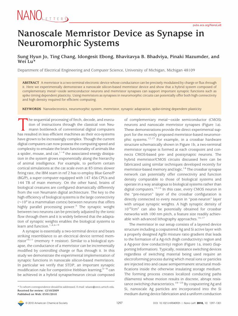
of complementary metal-oxide semiconductor (CMOS)neurons and nanoscale memristor synapses (Figure 1a).These demonstrations provide the direct experimental sup-port for the recently proposed memristor-based neuromor-phic systems.12,13 For example, in a crossbar hardwarestructure schematically shown in Figure 1b, a two-terminalmemristor synapse is formed at each crosspoint and con-nects CMOS-based pre- and postsynaptic neurons. Thehybrid memristor/CMOS circuits discussed here can befabricated using similar techniques developed recently formemristor-based memory and logic.14 The crossbar synapsenetwork can potentially offer connectivity and functiondensity comparable to those of biological systems andoperate in a way analogous to biological systems rather thandigital computers.12,15 In this case, every CMOS neuron inthe “pre-neuron” layer of the crossbar configuration isdirectly connected to every neuron in “post-neuron” layerwith unique synaptic weights. A high synaptic density of1010/cm2 can also be potentially obtained for crossbarnetworks with 100 nm pitch, a feature size readily achiev-able with advanced lithography approaches.16,17
The memristor in our setup consists of a layered devicestructure including a cosputtered Ag and Si active layer witha properly designed Ag/Si mixture ratio gradient that leadsto the formation of a Ag-rich (high conductivity) region anda Ag-poor (low conductivity) region (Figure 1a, inset) (Sup-porting Information). Typically, resistance switching devicesregardless of switching material being used require anelectroforming process during which metal ions or particlesare injected into and cause semipermanent structural modi-fications inside the otherwise insulating storage medium.The forming process creates localized conducting paths(filaments) whose motion results in discrete, abrupt resis-tance switching characteristics.18-23 By cosputtering Ag andSi, nanoscale Ag particles are incorporated into the Simedium during device fabrication and a uniform conduction
*To whom correspondence should be addressed. E-mail: [email protected] for review: 12/10/2009Published on Web: 03/01/2010
pubs.acs.org/NanoLett
© 2010 American Chemical Society 1297 DOI: 10.1021/nl904092h | Nano Lett. 2010, 10, 1297–1301
front between the Ag-rich and Ag-poor regions can beformed. As a result, the forming process can be eliminated.In addition, under applied bias the continuous motion ofthe conduction front in the cosputtered memristor devicereplaces discrete, localized conducting filament forma-tion22 and results in reliable “analog” switching behaviors(Figure 1c).
Figure 1c shows the measured device current i(t) (bluelines) as a function of the applied voltage across the mem-ristor v(t) for five consecutive positive voltage sweeps andfive consecutive negative voltage sweeps. Distinct fromdevices that show abrupt conductance jumps,18-23 here theconductance continuously increases (decreases) during thepositive (negative) voltage sweeps, and the I-V slope of eachsubsequent sweep picks up where the last sweep left off. Infact, the device I-V can be well fitted by a simple memristorcircuit model11 (orange lines, Figure 1c)
Here w(t) stands for the normalized position of theconduction front between the Ag-rich and Ag-poor regions
within the active device layer and has the value between 0and 1. Upon the application of a positive voltage bias, Agions move from the Ag-rich region to the Ag-poor region andincreases w, and vice versa. As w(t) approaches to 0(1), thedevice reaches the lowest (highest) conductance state withresistance of ROFF (RON). In this model we further assumedthe position w(t) is a linear function of the flux-linkage �(t)) ∫v(t)dt through the device. Equation 1 can then berewritten as
This is the equation for a flux-controlled memristor10 andG(�(t)) is the so-called memductance. In addition, for thedevices studied here bias voltages with amplitude < VT ) 2.2V are not sufficient to drive the Ag ions inside the a-Si matrixand have negligible effect on the memristor resistance. Thethreshold effect and the value of the threshold voltage VT
have been consistently obtained in all the devices tested inthis study.
The calculated current values during the voltage sweepsbased on the memristor model discussed above were shownas orange lines in Figure 1c together with the measuredcurrent (blue lines). The inset to Figure 1c shows the values
FIGURE 1. Nanoscale memristor characteristics and its application as a synapse. (a) Schematic illustration of the concept of using memristorsas synapses between neurons. The insets show the schematics of the two-terminal device geometry and the layered structure of the memristor.(b) Schematic of a neuromorphic with CMOS neurons and memristor synapses in a crossbar configuration. (c) Measured (blue lines) andcalculated (orange lines) I-V characteristics of the memristor. Inset: calculated (orange lines) and extracted (blue lines) values of the normalizedAg front position w during positive DC sweeps. (d) The current and voltage data versus time for the device in (c) highlighting the change incurrent in sequential voltage sweeps.
i(t) ) 1RONw(t) + ROFF(1 - w(t))
v(t) (1)
i(t) ) G(�(t))v(t) (2)
© 2010 American Chemical Society 1298 DOI: 10.1021/nl904092h | Nano Lett. 2010, 10, 1297-–1301
of w(t) (orange lines) used to calculate the current during thefive consecutive positive voltage sweeps by assuming w(t)to be a linear function of the flux-linkage �. In addition, thevalues of w(t) can also be directly extracted from the datausing eq 1 and are shown in the inset to Figure 1c as theblue lines. The relative good agreements between the cal-culated and the measured values in i(t) and w(t) verify thatthe device characteristics above the threshold voltage canindeed be explained by the memristor-model using eqs 1and 2, where the front position is roughly a linear functionof the flux-linkage �(t) ) ∫v(t)dt. However, strictly speakingthe device is not a true memristor due to the threshold effectbut falls in the more broadly defined memristive devicecategory.24 On the other hand, the threshold effect makesit possible to perform nondisturbing read of the device stateby using read pulses with Vread < VT and can in fact bebeneficial in practical applications.
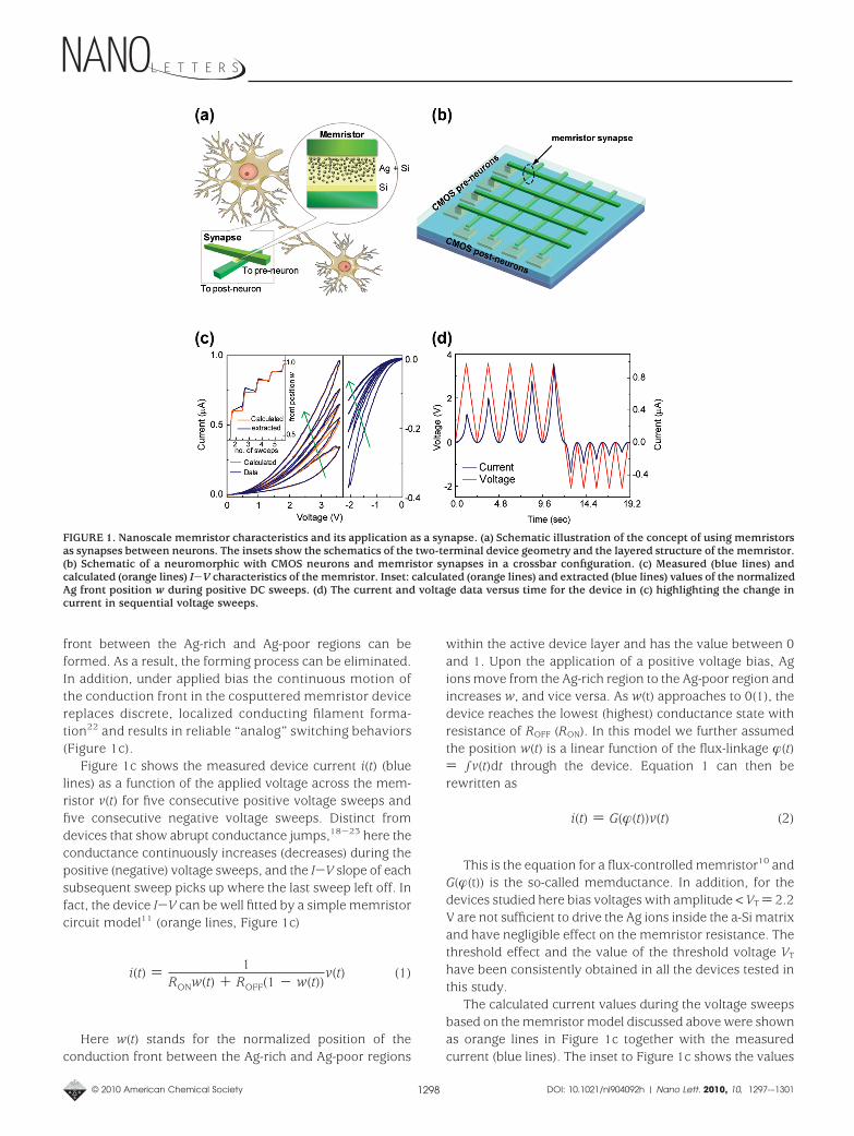
The flux-controlled memristor model suggests that thedevice conductance (memductance) can be incrementallyadjusted by tuning the duration and sequence of the appliedprogramming voltage. Figure 2a shows the results when thedevice was programmed by a series of 100 identical positive(3.2 V, 300 µs) pulses followed by a series of 100 identicalnegative voltage pulses (-2.8 V, 300 µs). The device con-ductance (represented by the measured current at a smallread voltage of 1 V) was measured after each programmingpulse. As expected from the DC characteristics of the device,the application of positive potentiating voltage pulses (P)incrementally increases the memristor conductance, and theapplication of negative depressing voltage pulses (D) incre-mentally decreases the memristor conductance. We notethat unlike results from devices with abrupt switchingcharacteristics where the programming signals control thefinal device state,22 here the flux-linkage �(t) during eachprogramming pulse controls the relative change of thememristor conductance. This effect was further demon-strated in Figure 2b. Here mixed positive (P) and negative(D) voltage pulses with constant pulse height but differentpulse widths were applied to the device and the change inmemristor conductance ∆G were measured and recordedafter each P/D pulse. A clear correlation between ∆G andthe pulse width of the applied P/D signals was observed; theapplication of a longer positive (negative) pulse resulted ina larger increase (decrease) of memristor conductance, andvice versa.
These results suggest the memristor devices are capableto emulate the biological synapses with properly designedCMOS neuron components to provide local programmingvoltages with controlled pulse width and height. For ex-ample, to demonstrate advanced synaptic functions such asSTDP, an important synaptic adaptation rule for competitiveHebbian learning that demands the change of synapticweight to be a strong function of the timing of the pre/postneuron spikes,6-8 we have implemented a CMOS neu-ron circuit to convert the relative timing information of the
neuron spikes into pulse width information seen by thememristor synapse (Supporting Information). Briefly, theneuron circuit consists of two CMOS based integrate-and-fire neurons25 connected by a nanoscale memristor withactive device area of 100 nm × 100 nm. The neuron circuitinvolves a mixed analog-digital design and employs a timedivision multiplexing (TDM) approach with globally synchro-nized time frames to convert the timing information into apulse width.12 Specifically, the neuron circuit generates apotentiating (depressing) pulse across the memristor syn-apse when the presynaptic neuron spikes before (after) thepostsynaptic neuron, with the pulse width being an expo-nentially decaying function of the relative neuron spiketiming ∆t ) tpre - tpost, where tpre (tpost) is the time when thepresynaptic neuron (postsynaptic neuron) spikes (SupportingInformation).
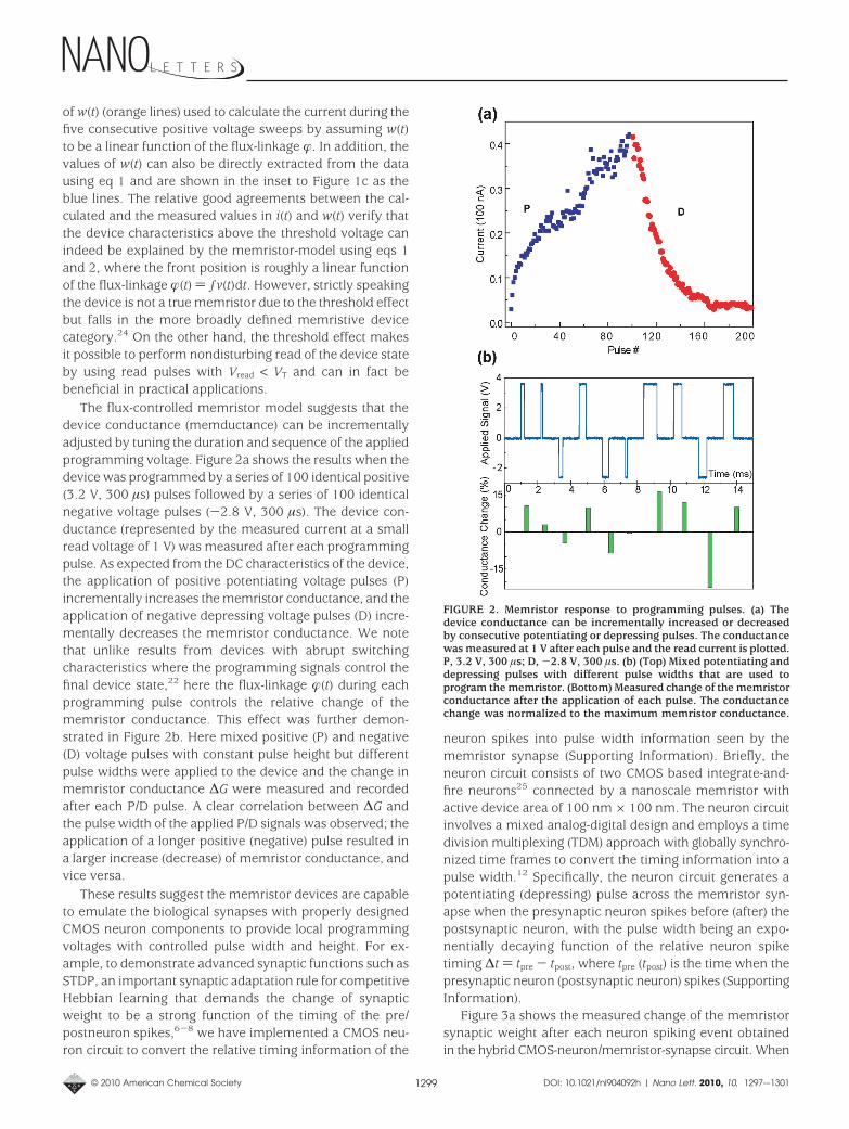
Figure 3a shows the measured change of the memristorsynaptic weight after each neuron spiking event obtainedin the hybrid CMOS-neuron/memristor-synapse circuit. When
FIGURE 2. Memristor response to programming pulses. (a) Thedevice conductance can be incrementally increased or decreasedby consecutive potentiating or depressing pulses. The conductancewas measured at 1 V after each pulse and the read current is plotted.P, 3.2 V, 300 µs; D, -2.8 V, 300 µs. (b) (Top) Mixed potentiating anddepressing pulses with different pulse widths that are used toprogram the memristor. (Bottom) Measured change of the memristorconductance after the application of each pulse. The conductancechange was normalized to the maximum memristor conductance.
© 2010 American Chemical Society 1299 DOI: 10.1021/nl904092h | Nano Lett. 2010, 10, 1297-–1301
the preneuron spikes before (after) the postneuron, thememristor synaptic weight increases (decreases). In addi-tion, the change in the synaptic weight versus the spiketiming difference ∆t can be well fitted with exponentialdecay functions, verifying that STDP characteristics similarto that of biological synaptic systems (e.g., Figure 3b) canindeed be obtained in memristor synapses.7,8
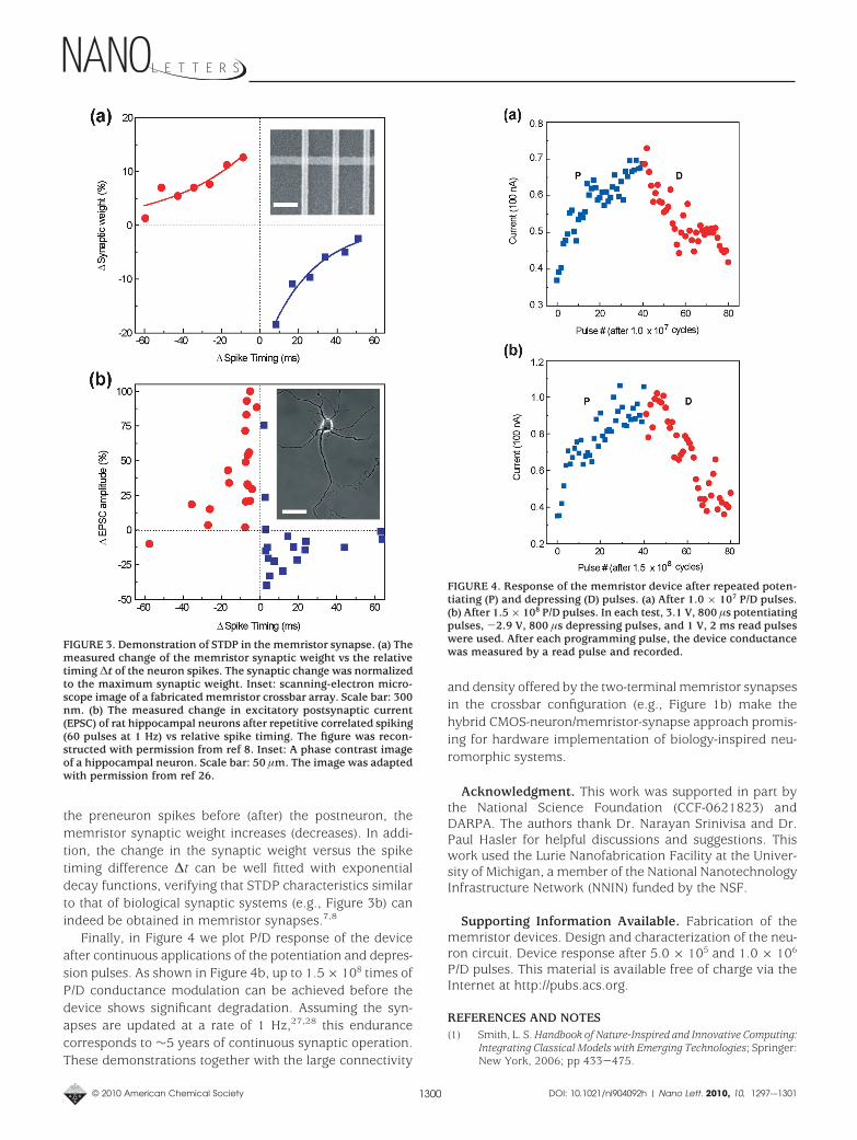
Finally, in Figure 4 we plot P/D response of the deviceafter continuous applications of the potentiation and depres-sion pulses. As shown in Figure 4b, up to 1.5 × 10⁸ times ofP/D conductance modulation can be achieved before thedevice shows significant degradation. Assuming the syn-apses are updated at a rate of 1 Hz,27,28 this endurancecorresponds to ∼5 years of continuous synaptic operation.These demonstrations together with the large connectivity
and density offered by the two-terminal memristor synapsesin the crossbar configuration (e.g., Figure 1b) make thehybrid CMOS-neuron/memristor-synapse approach promis-ing for hardware implementation of biology-inspired neu-romorphic systems.
Acknowledgment. This work was supported in part bythe National Science Foundation (CCF-0621823) andDARPA. The authors thank Dr. Narayan Srinivisa and Dr.Paul Hasler for helpful discussions and suggestions. Thiswork used the Lurie Nanofabrication Facility at the Univer-sity of Michigan, a member of the National NanotechnologyInfrastructure Network (NNIN) funded by the NSF.
Supporting Information Available. Fabrication of thememristor devices. Design and characterization of the neu-ron circuit. Device response after 5.0 × 10⁵ and 1.0 × 10⁶
P/D pulses. This material is available free of charge via theInternet at http://pubs.acs.org.
REFERENCES AND NOTES(1) Smith, L. S. Handbook of Nature-Inspired and Innovative Computing:
Integrating Classical Models with Emerging Technologies; Springer:New York, 2006; pp 433-475.
FIGURE 3. Demonstration of STDP in the memristor synapse. (a) Themeasured change of the memristor synaptic weight vs the relativetiming ∆t of the neuron spikes. The synaptic change was normalizedto the maximum synaptic weight. Inset: scanning-electron micro-scope image of a fabricated memristor crossbar array. Scale bar: 300nm. (b) The measured change in excitatory postsynaptic current(EPSC) of rat hippocampal neurons after repetitive correlated spiking(60 pulses at 1 Hz) vs relative spike timing. The figure was recon-structed with permission from ref 8. Inset: A phase contrast imageof a hippocampal neuron. Scale bar: 50 µm. The image was adaptedwith permission from ref 26.
FIGURE 4. Response of the memristor device after repeated poten-tiating (P) and depressing (D) pulses. (a) After 1.0 × 10⁷ P/D pulses.(b) After 1.5 × 10⁸ P/D pulses. In each test, 3.1 V, 800 µs potentiatingpulses, -2.9 V, 800 µs depressing pulses, and 1 V, 2 ms read pulseswere used. After each programming pulse, the device conductancewas measured by a read pulse and recorded.
© 2010 American Chemical Society 1300 DOI: 10.1021/nl904092h | Nano Lett. 2010, 10, 1297-–1301
(2) Ananthanarayanan, R.; Esser, S. K.; Simon, H. D.; Modha, D. S.Proceedings of 2009 IEEE/ACM Conference High PerformanceNetworking Computing; Portland, OR, November, 2009.
(3) Izhikevich, E. M.; Edelman, G. M. Proc. Natl. Acad. Sci. U.S.A.2008, 105, 3593–3598.
(4) Indiveri, G.; Chicca, E.; Douglas, R. IEEE Trans. Neural Networks2006, 17, 211–221.
(5) Tang, Y.; Nyengaard, J. R.; De Groot, D. M. G.; Gundersen, H. J. G.Synapse 2001, 41, 258–273.
(6) Hebb, D. O. The organization of behavior. A neuropsychologicaltheory; John Wiley and Sons, Inc.: New York, 1949.
(7) Song, S.; Miller, K. D.; Abbott, L. F. Nature Neurosci. 2000, 3, 919–926.
(8) Bi, G. Q.; Poo, M. M. J. Neurosci. 1998, 18, 10464–10472.(9) Douglas, R.; Mahowald, M.; Mead, C. Annu. Rev. Neurosci. 1995,
18, 255–281.(10) Chua, L. O. IEEE Trans. Circuit Theory 1971, 18, 507–519.(11) Strukov, D. B.; Snider, G. S.; Stewart, D. R.; Williams, R. S. Nature
2008, 453, 80–83.(12) Snider, G. S. IEEE/ACM International Symposium on Nanoscale
Architectures; Anaheim, CA, June, 2008; 85-92.(13) Pershin, Y. V.; La Fontaine, S.; Di Ventra, M. Phys. Rev. E 2009,
80, No. 021926.(14) Borghetti, J.; Li, Z.; Straznicky, J.; Li, X.; Ohlberg, D. A. A.; Wu,
W.; Stewart, D. R.; Williams, R. S. Proc. Natl. Acad. Sci. U.S.A.2009, 106, 1699–1703.
(15) Lu, W.; Lieber, C. M. Nat. Mater. 2007, 6, 841–850.
(16) Green, J. E.; Choi, J. W.; Boukai, A.; Bunimovich, Y.; Johnston-Halperin, E.; DeIonno, E.; Luo, Y.; Sheriff, B. A.; Xu, K.; Shin, Y. S.;Tseng, H. R.; Stoddart, J. F.; Heath, J. R. Nature 2007, 445, 414–417.
(17) Jung, G. Y.; Johnston-Halperin, E.; Wu, W.; Yu, Z. N.; Wang, S. Y.;Tong, W. M.; Li, Z. Y.; Green, J. E.; Sheriff, B. A.; Boukai, A.;Bunimovich, Y.; Heath, J. R.; Williams, R. S. Nano Lett. 2006, 6,351–354.
(18) Kund, M.; Beitel, G.; Pinnow, C. U.; Rohr, T.; Schumann, J.;Symanczyk, R.; Ufert, K. D.; Muller, G. 2005 IEEE InternationalElectron Devices Meeting; Technical Digest: Washington, DC,December, 2005; pp 773-776.
(19) Waser, R.; Aono, M. Nat. Mater. 2007, 6, 833–840.(20) Yang, J. J.; Pickett, M. D.; Li, X. M.; Ohlberg, D. A. A.; Stewart,
D. R.; Williams, R. S. Nat. Nanotechnol. 2008, 3, 429–433.(21) Jo, S. H.; Lu, W. Nano Lett. 2008, 8, 392–397.(22) Jo, S. H.; Kim, K. H.; Lu, W. Nano Lett. 2009, 9, 496–500.(23) Liu, M.; Abid, Z.; Wang, W.; He, X. L.; Liu, Q.; Guan, W. H. Appl.
Phys. Lett. 2009, 94, 233106.(24) Chua, L. O.; Kang, S. M. Proc. IEEE 1976, 64, 209–223.(25) Brette, R.; Gerstner, W. J. Neurophysiol. 2005, 94, 3637–3642.(26) Kaech, S.; Banker, G. Nat Protoc. 2006, 1, 2406–2415.(27) Lev-Ram, V.; Wong, S. T.; Storm, D. R.; Tsien, R. Y. Proc. Natl.
Acad. Sci. U.S.A. 2002, 99, 8389–8393.(28) Bear, M. F. Proc. Natl. Acad. Sci. U.S.A. 1996, 93, 13453–
13459.
© 2010 American Chemical Society 1301 DOI: 10.1021/nl904092h | Nano Lett. 2010, 10, 1297-–1301