naval postgraduate school - dtic.mil · naval postgraduate school ... different locations on the...
TRANSCRIPT

NAVAL
POSTGRADUATE SCHOOL
MONTEREY, CALIFORNIA
THESIS
Approved for public release; distribution is unlimited
DYNAMIC RESPONSE OF SOLDERED ELECTRONIC COMPONENTS UNDER IMPACT LOADING
by
Andrew Calvin Wood
December 2011
Thesis Advisor: Young W. Kwon Thesis Co-Advisor: Jarema M. Didoszak

THIS PAGE INTENTIONALLY LEFT BLANK

i
REPORT DOCUMENTATION PAGE Form Approved OMB No. 0704–0188 Public reporting burden for this collection of information is estimated to average 1 hour per response, including the time for reviewing instruction, searching existing data sources, gathering and maintaining the data needed, and completing and reviewing the collection of information. Send comments regarding this burden estimate or any other aspect of this collection of information, including suggestions for reducing this burden, to Washington headquarters Services, Directorate for Information Operations and Reports, 1215 Jefferson Davis Highway, Suite 1204, Arlington, VA 22202–4302, and to the Office of Management and Budget, Paperwork Reduction Project (0704–0188) Washington DC 20503. 1. AGENCY USE ONLY (Leave blank)
2. REPORT DATE December 2011
3. REPORT TYPE AND DATES COVERED Master’s Thesis
4. TITLE AND SUBTITLE Dynamic Response of Soldered Electronic Components under Impact Loading
5. FUNDING NUMBERS
6. AUTHOR(S) Andrew Calvin Wood 7. PERFORMING ORGANIZATION NAME(S) AND ADDRESS(ES)
Naval Postgraduate School Monterey, CA 93943–5000
8. PERFORMING ORGANIZATION REPORT NUMBER
9. SPONSORING /MONITORING AGENCY NAME(S) AND ADDRESS(ES) N/A
10. SPONSORING/MONITORING AGENCY REPORT NUMBER
11. SUPPLEMENTARY NOTES The views expressed in this thesis are those of the author and do not reflect the official policy or position of the Department of Defense or the U.S. Government. IRB Protocol Number: N/A
12a. DISTRIBUTION / AVAILABILITY STATEMENT Approved for public release; distribution is unlimited
12b. DISTRIBUTION CODE A
13. ABSTRACT
The objective of this research was to analyze the effects of impact loading on electronic component failure. A standard fiberglass composite printed circuit board (PCB) card was used in two impact tests. The first test consisted of a PCB card with four adhered strain gauges, which were mounted inside an aluminum box fabricated for testing. Impact testing was conducted with weights ranging from 0 to 30 lb., and the corresponding strain values were recorded. For the second set of impact tests, a new circuit card was mounted inside the aluminum box. The new circuit card maintained the same dimensions, but no strain gauges were attached. Solder joints were placed at nine different locations on the card, and testing was conducted to determine the impact load at solder joint failure. Both visual and resistance inspections were conducted after each impact. After seven drop tests were conducted, no failure had been detected. This lack of failure was attributed to the rigidity and substantial nature of the aluminum box used in testing. Upon completion of both impact tests, two Finite Element Method (FEM) models were built. The first FEM model represented a scaled version of the PCB card, four solder joints, and a silicon computer chip. Strain data from the PCB card testing was input into the model, and a corresponding solder joint strain was calculated. The second FEM model was a full-scale version of the aluminum box and mounted circuit card. A force was applied to the box, and the various stains were recorded on the PCB card. The collection of this data has helped to establish a valuable relationship between the strains in PCB cards and solder joints, and it will increase the understanding of electronic component failure under impact loading conditions.
14. SUBJECT TERMS solder joint, impact loading, electronic component failure 15. NUMBER OF
PAGES 81
16. PRICE CODE
17. SECURITY CLASSIFICATION OF REPORT
Unclassified
18. SECURITY CLASSIFICATION OF THIS PAGE
Unclassified
19. SECURITY CLASSIFICATION OF ABSTRACT
Unclassified
20. LIMITATION OF ABSTRACT
UU NSN 7540–01–280–5500 Standard Form 298 (Rev. 2–89) Prescribed by ANSI Std. 239–18

ii
THIS PAGE INTENTIONALLY LEFT BLANK

iii
Approved for public release; distribution is unlimited
DYNAMIC RESPONSE OF SOLDERED ELECTRONIC COMPONENTS UNDER IMPACT LOADING
Andrew Calvin Wood Lieutenant, United States Navy
B.S., United States Naval Academy, 2005
Submitted in partial fulfillment of the requirements for the degree of
MASTER OF SCIENCE IN MECHANICAL ENGINEERING
from the
NAVAL POSTGRADUATE SCHOOL December 2011
Author: Andrew Calvin Wood
Approved by: Young W. Kwon Thesis Advisor
Jarema M. Didoszak Thesis Co-Advisor
Knox T. Millsaps Chair, Department of Mechanical and Aerospace Engineering

iv
THIS PAGE INTENTIONALLY LEFT BLANK

v
ABSTRACT
The objective of this research was to analyze the effects of impact loading on electronic
component failure. A standard fiberglass composite printed circuit board (PCB) card was
used in two impact tests. The first test consisted of a PCB card with four adhered strain
gauges, which were mounted inside an aluminum box fabricated for testing. Impact
testing was conducted with weights ranging from 0 to 30 lb., and the corresponding strain
values were recorded. For the second set of impact tests, a new circuit card was mounted
inside the aluminum box. The new circuit card maintained the same dimensions, but no
strain gauges were attached. Solder joints were placed at nine different locations on the
card, and testing was conducted to determine the impact load at solder joint failure. Both
visual and resistance inspections were conducted after each impact. After seven drop
tests were conducted, no failure had been detected. This lack of failure was attributed to
the rigidity and substantial nature of the aluminum box used in testing. Upon completion
of both impact tests, two Finite Element Method (FEM) models were built. The first
FEM model represented a scaled version of the PCB card, four solder joints, and a silicon
computer chip. Strain data from the PCB card testing was input into the model, and a
corresponding solder joint strain was calculated. The second FEM model was a full-scale
version of the aluminum box and mounted circuit card. A force was applied to the box,
and the various stains were recorded on the PCB card. The collection of this data has
helped to establish a valuable relationship between the strains in PCB cards and solder
joints, and it will increase the understanding of electronic component failure under
impact loading conditions.

vi
THIS PAGE INTENTIONALLY LEFT BLANK

vii
TABLE OF CONTENTS
I. INTRODUCTION .......................................................................................................1 A. BACKGROUND ..............................................................................................1
1. Ground Combat Application ..............................................................1 2. Maritime Combat Application ............................................................2
B. LITERATURE SURVEY ................................................................................2 1. Vibration Effects on Solder Joint Failure ..........................................2 2. Varying Strain Rates and Solder Joint Failure .................................3 3. Drop Impact Analysis on Sn-Ag-Cu Solder Joints ...........................4
C. OBJECTIVE OF STUDY ...............................................................................4
II. EXPERIMENTAL .......................................................................................................7 A. IMPACT TESTING FOR STRAIN ...............................................................7
1. Drop Weight Vertical Impact Test Apparatus ..................................7 2. Data Collection .....................................................................................8 3. Strain Gauges .......................................................................................9 4. Test Setup and Procedures ................................................................11
B. IMPACT TESTING FOR SOLDER JOINT FAILURE ...........................12 1. Preliminary PCB Card Design with BGA Solder Joints ................12 2. Secondary PCB Card Design with Resistor Packs..........................14 3. Tertiary PCB Card Design with Soldered Bridge ..........................16 4. Test Setup and Procedures ................................................................16
III. ANALYTICAL ...........................................................................................................19 A. FEM MODEL OF SOLDERED ELECTRONIC COMPONENT ............19 B. FEM MODEL OF BOX WITH MOUNTED PCB CARD ........................21
IV. RESULTS AND DISCUSSION ................................................................................25 A. LONGITUDINAL AND LATERAL STRAIN IN PCB CARD .................25
1. Longitudinal and Lateral Strain as a Function of Time ................25 2. Longitudinal and Lateral Strain as a Function of Added
Weight .................................................................................................33 B. FEM ANALYSIS OF SOLDERED ELECTRONIC COMPONENT ......38 C. FEM ANALYSIS OF BOX WITH MOUNTED PCB CARD ...................45 D. STRAIN RELATIONSHIP BETWEEN PCB CARD AND SOLDER
JOINT .............................................................................................................56
V. CONCLUSIONS AND RECOMMENDATIONS ...................................................59 LIST OF REFERENCES ......................................................................................................61
INITIAL DISTRIBUTION LIST .........................................................................................63

viii
THIS PAGE INTENTIONALLY LEFT BLANK

ix
LIST OF FIGURES
Figure 1. Drop weight vertical impact test apparatus. .......................................................7 Figure 2. Drop weight and Al box. ....................................................................................8 Figure 3. Trigger mechanism and sensor. .........................................................................9 Figure 4. Rectangular, three element 45º rosette (After [6]). ..........................................10 Figure 5. Strain gauges mounted on PCB card. ..............................................................10 Figure 6. PCB card quadrant numbers. ...........................................................................11 Figure 7. PCB card and Al bracket mounted for testing. ................................................12 Figure 8. PGA component bottom view (After [7]). .......................................................13 Figure 9. BGA component prior to assembly (After [8]). ...............................................14 Figure 10. PCB card mounting pad w/o resistor pack. ......................................................15 Figure 11. Resistor pack (After [9]). .................................................................................15 Figure 12. PCB card with soldered bridge. .......................................................................16 Figure 13. FLUKE™ multimeter. .....................................................................................17 Figure 14. ANSYS™ FEM model of soldered electronic component. .............................19 Figure 15. SolidWorks™ wire frame view of Al box and mounted PCB card. ................22 Figure 16. ANSYS™ FEM model of Al box and mounted PCB card. .............................22 Figure 17. ANSYS™ tabular data input. ..........................................................................23 Figure 18. ANSYS™ plot of force vs. time for a 0.1 s interval. .......................................24 Figure 19. Longitudinal and lateral strain with 0 lb. added weight. ..................................26 Figure 20. Longitudinal and lateral strain with 5 lb. added weight. ..................................27 Figure 21. Longitudinal and lateral strain with 10 lb. added weight. ................................28 Figure 22. Longitudinal and lateral strain with 15 lb. added weight. ................................29 Figure 23. Longitudinal and lateral strain with 20 lb. added weight. ................................30 Figure 24. Longitudinal and lateral strain with 25 lb. added weight. ................................31 Figure 25. Longitudinal and lateral strain with 30 lb. added weight. ................................32 Figure 26. Max Longitudinal strain with 0 lb. added weight. ...........................................33 Figure 27. Max Longitudinal strain with 5 lb. added weight. ...........................................34 Figure 28. Max Longitudinal strain with 10 lb. added weight. .........................................34 Figure 29. Max Longitudinal strain with 15 lb. added weight. .........................................35 Figure 30. Max Longitudinal strain with 20 lb. added weight. .........................................35 Figure 31. Max Longitudinal strain with 25 lb. added weight. .........................................36 Figure 32. Max Longitudinal strain with 30 lb. added weight. .........................................36 Figure 33. Max Longitudinal and lateral strain as a function of added weight. ................37 Figure 34. Max principal strain. ........................................................................................39 Figure 35. Normal strain in the longitudinal (Y) axis. ......................................................40 Figure 36. Normal strain in the lateral (X) axis. ...............................................................40 Figure 37. Shear strain in the XY plane. ...........................................................................41 Figure 38. Shear strain in the YZ plane. ............................................................................41 Figure 39. Max principal strain on solder joint. ................................................................42 Figure 40. Normal strain on solder joint in the longitudinal (Y) axis. ..............................43 Figure 41. Normal strain on solder joint in the lateral (X) axis. .......................................43 Figure 42. Shear strain on solder joint in the XY plane. ...................................................44

x
Figure 43. Shear strain on solder join in the YZ plane. .....................................................44 Figure 44. Max principal strain in Al box and PCB card. .................................................47 Figure 45. Normal strain in the longitudinal (X) axis in Al box and PCB card. ...............48 Figure 46. Normal strain in the lateral (Y) axis in Al box and PCB card. ........................49 Figure 47. Max shear strain in Al box and PCB card. .......................................................50 Figure 48. Shear strain in XY plane on Al box and PCB card. .........................................51 Figure 49. Shear strain in XZ plane on Al box and PCB card. .........................................52 Figure 50. Max principal strain on PCB card. ...................................................................53 Figure 51. Normal strain in the longitudinal (X) axis on PCB card. .................................53 Figure 52. Normal strain in the lateral (Y) axis on PCB card. ..........................................54 Figure 53. Max shear strain on PCB card. ........................................................................54 Figure 54. Shear strain in XY plane on PCB card. ............................................................55 Figure 55. Shear strain in XZ plane on PCB card. ............................................................55 Figure 56. Theoretical relationship between normal and shear strains in PCB cards
and corresponding solder joints. ......................................................................57

xi
LIST OF TABLES
Table 1. FEM model component material properties. ...................................................20 Table 2. FEM model deformation inputs. ......................................................................21 Table 3. FEM model dimensions. ..................................................................................21 Table 4. Al box and PCB card dimensions. ...................................................................23 Table 5. Max Longitudinal and lateral strain values. .....................................................37 Table 6. Max longitudinal, lateral, and principal strain values for the model. ..............38 Table 7. Shear in the XY and YZ plane. ........................................................................38 Table 8. Max longitudinal, lateral, and principal strain values in ANSYS™ PCB
card. ..................................................................................................................45 Table 9. XY, XZ, and max shear strain values in ANSYS™ PCB card. .......................45 Table 10. Shear in the XY and YZ plane, and max shear strain for the model. ..............46 Table 11. Theoretical and ANSYS™ strain comparison. ................................................58

xii
THIS PAGE INTENTIONALLY LEFT BLANK

xiii
LIST OF ACRONYMS AND ABBREVIATIONS
Ag Element symbol for silver
Al Element symbol for aluminum BGA Ball-Grid Array
CAD Computer Aided Design Cu Element symbol for copper
ε Strain (mm/mm)
µε Microstrain (mm/mm) FEM Finite Element Method
ft Feet kN Kilonewton
IED Improvised Explosive Device in Inches
kg Kilogram l Length
lb.(s) Pound(s) MPa Megapascal
mm Millimeters ms Milliseconds
Pb Element symbol for lead PCB Printed Circuit Board PGA Pin-Grid Array
s Seconds Si Element symbol for silicon
Sn Element symbol for tin

xiv
THIS PAGE INTENTIONALLY LEFT BLANK

xv
ACKNOWLEDGMENTS
I would like to thank Professor Young Kwon for his guidance and patience
throughout the course of this thesis work. I would also like to thank Professor Jarema
Didoszak for his insight in completing this research. Finally, I would like to thank my
wife and best friend, Lindy, for all her love and support. God has truly blessed me and
my family during our time here in Monterey.

xvi
THIS PAGE INTENTIONALLY LEFT BLANK

1
I. INTRODUCTION
A. BACKGROUND
The vast majority of failures in electronic equipment are due to failures in the
solder joint that connects the electronic component to the printed circuit board (PCB).
With the increased use of improvised explosive devices (IED), we have seen failure of
electronic components in many military applications [1]. Often, the boxes or cases
holding these components withstood the blast impact without failure. However, the
failure is found to be occurring at the solder joint interface between the component itself
and PCB mounted inside the equipment box or case.
Similar results have been seen in Naval application when ships have impacted
underwater obstructions or have been in close proximity to an underwater explosion. The
integrity of the ship and its equipment housings remains intact, but the solder joints
attaching the electronic components to the PCB cards are failing. Therefore, continued
research on the effect of impact and shock loading on electronic component failure is
beneficial to the design of electronic equipment and the formulation of a criterion for
predicting failure of solder joints.
1. Ground Combat Application
The wars in Iraq and Afghanistan reveal vulnerabilities in U.S. Armed Forces
defenses against IEDs. As a result, building and designing war fighting equipment to
withstand IEDs has become a high priority. Military vehicles and equipment are now
able to withstand much greater impact forces due to close range explosions caused by
IEDs. However, failure is still occurring in the onboard electronic equipment due to the
shock and impact forces resulting from the explosion [1]. More specifically, failure is
occurring at the PCB card and solder joint interface of individual electronic components.
The vehicles and the boxes holding the PCB cards are remaining intact, but the
components themselves are breaking free from their soldered mounts.

2
2. Maritime Combat Application
Where ground forces face the challenge of overcoming IEDs and the damage they
inflict on equipment and personnel, the Navy is exposed to an entirely different set of
threatening devices. Underwater mines and torpedoes each have the ability to inflict
catastrophic damage to a ship and its crew. In addition, uncharted sea mounts and shoal
water present very real threats to the structural integrity of a war ship. To improve design
and survivability, one ship from each class of war ship will normally undergo shock
trials. The data gathered from each shock test provides valuable information to ship
designers and engineers on how to improve the survivability of that vessel. However,
despite the advancements made in structural integrity and survivability following an
underwater explosion or impact, electronic components are still experiencing failure at
the PCB card and solder joint interface.
B. LITERATURE SURVEY
1. Vibration Effects on Solder Joint Failure
Military environments expose war fighting equipment to numerous sources of
harmful vibrations. Over time, these vibrations cause failure at the PCB card and solder
joint interface. Though military grade equipment is often built to withstand these harsh
conditions, many of the components used are commercial-off-the-shelf (COTS). Celik
and Genc [1] state that the life expectancy of military grade electronics is 20 years, but
COTS electronics will only last 7 to 10 years.
Attempts have been made to reduce the effects of these harmful vibrations by
implementing vibration isolators. Though widely accepted as a solution to the problem
of premature solder joint failures do to vibration, Celik and Genc [1] argue that these
isolators have significant drawbacks. Their research suggests that the silicone used to
isolate the component to the PCB card is not appropriate for high temperature
environments. In addition, the adhesive will stiffen the component and cause excess
flexural stresses. Lastly, manufacture and repair are often cost prohibitive.
Celik and Genc [1] conducted vibration testing on axial leaded capacitors. They
found that the components could withstand more vibration as solder joint diameter

3
increased. Also, the length and width of the card had a direct effect on a components life
span. As the width of the PCB card increased and the length decreased, the components
saw a higher failure rate.
Celik and Genc [1] concluded that more computer simulation needs to be
conducted on electronic components prior to their introduction into the fleet. Significant
problems can be addressed through a computer modeling program long before it fails in
combat application. COTS electronic components have a life expectancy that is half that
of their military counterparts. However, sufficient simulation and testing is the first step
in fixing the problems caused by premature solder joint failure due to vibration.
2. Varying Strain Rates and Solder Joint Failure
Luteran [2] focused his research in the area constant and varying strain rates and
their effect on solder joint reliability. He conducted uniaxial testing to investigate the
mechanical behaviors of a solder joint under single and varying strain rate loading. He
determined that the elastic modulus of all test samples decreased as strain rate increased.
Conversely, he found that yield and ultimate strengths increased as a result of an
increased strain rate. It was also noted the fracture strains, ultimate strengths, and total
strain energy densities had higher values when tested with a fast strain rate followed by a
slow strain rate. A slow strain rate followed by a fast strain rate resulted in lower fracture
strains, ultimate strengths, and total strain energy densities. Luteran’s [2] research and
experimentation led to the establishment of a failure criteria for lead free solder joints
under varying strain rates.
Boyce et al. [3] studied the thermomechanical strain rate sensitivity of Sn-Pb
solder over a wide range of strain rates. Failure rates occurred between 1 ms and 1 hr.
They concluded that the standard Johnson-Cook constitutive model for strain rate
sensitivity was insufficient for representing observed behavior. Boyce et al. [3]
determined that a unified creep plasticity formulation offers an improved representation
of the observed behavior. They also concluded that there was an absence of significant
internal grain rotation, and that it consistent at all strain-rates.

4
3. Drop Impact Analysis on Sn-Ag-Cu Solder Joints
Pang and Che [4] discuss the complexities of drop test analysis and the dangers of
over simplifying Sn-Ag-Cu solder joint deformation response. Solder joint failure is a
combination of fatigue crack growth and brittle fracture of the intermetallic interfaces.
Oversimplification can lead to a misunderstanding of the actual cause of failure due to
drop impact testing. Pang and Che [4] use a split Hopkinson pressure bar (SHPB) test
system to study the solder joint failure due to impact loading.
Pang and Che [4] argue that during drop testing, dynamic hardening will occur in
the Sn-Ag-Cu solder joint. This hardening will cause the yield stress to rise several times
higher than the nominal yield stress in the Sn-Ag-Cu solder joint. This increase in
dynamic strength will cause strain cycling in the material and potentially lead to
premature fatigue failure. Conversely, if the impact loading is excessive, impact failure
strength of the intermetallic surface can lead to brittle failure.
Pang and Che [4] used multiple components in testing, and concluded that BGA
components had the highest failure rate. They concluded that the strain rate effect had a
large influence on the Sn-Ag-Cu solder joint reliability, and that lead free solder had a
higher failure rate than the solder with lead.
C. OBJECTIVE OF STUDY
The objective of this study is to examine the strain in the PCB card and its solder
joints, as a result of impact loading, in order to better understand failure in electronic
components. Due to their small size and inaccessibility, it is impractical and cost
prohibitive to directly mount strain gauges to many solder joints. Upon completion of
impact testing for strain in the PCB card, this study will attempt to establish a relationship
between the strains in the PCB card and the corresponding solder joint. A FEM model
representing a small cutout of the PCB card, four solder joints, and mounted silicon
processing chip will help to provide the data required to verify this relationship.
In addition, this study will use further impact testing to establish a relationship
between impact loading and solder joint failure. A second FEM model, a full-scale
representation of the aluminum (Al) box and mounted circuit card, will be used to verify

5
failure results. Once a relationship is established, this model will provide researchers
with an efficient means of modifying the box design. Quick and efficient modifications
to the computer model will help to determine how dimensional changes to the box affect
solder joint reliability.
Chapter II of this thesis describes the experimental impact testing for both strain
and solder joint failure. Chapter III introduces two FEM models representing a section of
the PCB card, solder joint and silicon chip, as well as the full-scale model of the Al box
and mounted PCB card. Chapter IV addresses the behaviors of both lateral and
longitudinal strain in the PCB card in addition to providing an analysis of both FEM
models. Chapter IV will also explore the relationship between the stresses in both the
PCB card and its corresponding solder joints. Chapter V will consist of both conclusions
and any furthering research recommendations.

6
THIS PAGE INTENTIONALLY LEFT BLANK

7
II. EXPERIMENTAL
A. IMPACT TESTING FOR STRAIN
1. Drop Weight Vertical Impact Test Apparatus
The impact test platform used for both experimental studies was a Drop Weight
Vertical Impact Test Apparatus pictured in Figure 1. The test rig consisted of a drop
weight with a 7.6 x 7.6 cm steel base, approximately 1.9 cm thick. The drop weight
allowed up to 30 lb. of added weight to be bolted to the apparatus. The drop weight was
raised to a height of 91.4 cm above the Al box. Upon release, the drop weight would fall
vertically and impact the Al box. Four guide rods with linear bearings insured a uniaxial
loading of the Al box upon impact. The test rig frame was constructed from an Al alloy.
Figure 1. Drop weight vertical impact test apparatus.

8
The Al box was designed and built to withstand repeated impacts without failure.
The box top dimensions are 27.9 x 27.9 cm with a thickness of 1.9 cm. The sides are all
10.2 cm tall with a thickness of 1.3 cm. The box is mounted to the test rig by way of two
vertical supports and four set screws. The drop weight is designed to impact the exact
center of the box top.
2. Data Collection
Data collection for all impact testing was conducted using LabVIEW™. Prior to
impact, a vertical trigger mechanism passes through a sensor and starts a data recorder.
1,000 samples of strain data are recorded over a 0.1 s time period. The software is set to
record at 10,000 Hz. Figure 2 and Figure 3 show the vertical trigger mechanism and the
sensor.
Figure 2. Drop weight and Al box.

9
Figure 3. Trigger mechanism and sensor.
3. Strain Gauges
The strain gauges used in both impact tests were three element, 45º rosettes
shown in Figure 4. The three readings collected from the elements are referred to as
gauge strain. The gauge strain must then be converted into principal strain by means of
the following transformation equations [5]:
𝜀! = 𝜀! + 𝜀!2 +
12
𝜀! − 𝜀! ! + 𝜀! − 𝜀! !
𝜀! = 𝜀! + 𝜀!2 −
12
𝜀! − 𝜀! ! + 𝜀! − 𝜀! !

10
Figure 4. Rectangular, three element 45º rosette (After [6]).
The strain gauges are mounted on the PCB card 90º from positioning shown in
Figure 4. This orientation will allow the center strain gauge element to align itself with
the x-axis. Therefore, 𝜀! is equal to 𝜀!. Figure 5 pictures the strain gauges mounted to
the PCB card and wired for impact testing.
Figure 5. Strain gauges mounted on PCB card.

11
Figure 6 depicts the four quadrants, beginning with number 1 in the lower right
and moving counter clockwise to number 4 in the lower left. The x-axis and y-axis will
be referred to as the lateral and longitudinal axis, respectively. Each strain gauge was
mounted in the center of its quadrant and numbered accordingly.
Figure 6. PCB card quadrant numbers.
4. Test Setup and Procedures
The impact test for strain required the PCB card with strain gauges to be mounted
inside the Al box as shown in Figure 7. The PCB card was bolted to a small Al bracket,
and the assembled PCB card and bracket were then secured to the Al box. This proved to
be the most efficient means of switching the PCB cards used in testing. Securing the
PCB card to the bracket required both a screw driver and an adjustable wrench to tighten
the five bolts, washers and nuts. The Al bracket mounted to the Al box using four hex-
head screws that were easily accessible from the bottom opening with an Allen wrench.
For each impact test, the drop weight was raised to a height of 91.4 cm above the
Al box. The drop weight was held in place by a steel pin while the data collection was
1
2
4
3
x
y

12
prepared. Hearing protection and a safety observer were required at all times. A ladder
was necessary to both insert and remove the steel pin used to hold the drop weight. Once
the pin was removed, the drop weight would fall and trigger the sensor to collect strain
data. Weight was added in 5 lb. increments, starting with no additional weight added and
finishing with 30 lb. of weight added. Altogether, seven drop tests were conducted and
strain data was collected for each.
Figure 7. PCB card and Al bracket mounted for testing.
B. IMPACT TESTING FOR SOLDER JOINT FAILURE
1. Preliminary PCB Card Design with BGA Solder Joints
Determining solder joint failure is a difficult process due in part to the small size
and location of each joint. Preliminary research was focused on the ball-grid array
(BGA) solder joints manufacturing process, as many military applications have begun
using BGA technology in the design and manufacture of their electronic components.
The traditional solder joint process is known as pin-grid array (PGA). PGA
components have metal pins that must be fit into corresponding holes on the PCB card.

13
Once the pins have been aligned and pushed through the holes, they are soldered to the
bottom side of the PCB card. The soldering connects the pins to connectors called traces.
Traces are conductive paths embedded into the PCB card. Once secured and soldered in
place, any excess metal wire on the pin is trimmed flush with the solder joint. Figure 8
depicts a typical PGA component.
Figure 8. PGA component bottom view (After [7]).
BGA components allow for automated precision in the manufacturing process.
Contact pads flush with the surface of the PCB card are connected to each of the traces.
A BGA component will have corresponding contact pads on its bottom side. The
automated process allows a machine to simultaneously lay an array of solder beads to
each of PCB cards contact pads. The BGA component is then aligned and joined to the
PCB card by way of the heating the solder beads. Figure 9 shows a standard BGA
component prior to assembly.

14
Figure 9. BGA component prior to assembly (After [8]).
The preliminary design for the circuit card used in testing for solder joint failure
was to use a BGA component soldered to a standard PCB card. However, determining
failure in the interior solder joints proved to be a difficult and labor-intensive process. In
addition, it was cost prohibitive to design and build multiple BGA test cards.
2. Secondary PCB Card Design with Resistor Packs
In order to simulate the solder joint interface of a BGA component, the decision
was made to design a test card using resistor packs with corresponding mounting pads
embedded in the PCB card. The mounting pads connect to the traces on the PCB card, as
shown in Figure 10. The traces from each mounting pad leads to an exposed test point on
the PCB card. These test points allow the resistance to be measured across each resistor
by use of a mulitmeter. This enables both a visual and resistance inspection to be
conducted after each impact test.

15
Figure 10. PCB card mounting pad w/o resistor pack.
However, after design and fabrication of the PCB card was complete, an
insufficient number of resistor packs, similar to those in Figure 11, were available for
procurement due to manufacturing constraints. The 10 PCB cards ordered required nine
resistor packs each. A total of 90 resistor packs were required, but the manufacturer only
possessed four resistor packs. Thus, a third testing design was necessary.
Figure 11. Resistor pack (After [9]).

16
3. Tertiary PCB Card Design with Soldered Bridge
A decision was made to proceed with the current PCB card with the resistor pack
mounting pads. In order to test for solder joint failure, a ball of solder was welded across
the resistor pack mounting pads embedded into the PCB card, as shown in Figure 12.
Figure 12. PCB card with soldered bridge.
This soldered bridge solution satisfied the requirement for both visual and
resistance inspections to be conducted after each impact test.
4. Test Setup and Procedures
Impact testing for solder joint failure was conducted in a similar fashion to the
impact testing for strain. The PCB card with nine soldered bridges was mounted to the
Al bracket and in turn mounted inside the Al box, as shown in Figure 7. Weight was
added in 5 lb. increments, starting with 0 lb. of weight added and finishing with 30 lb. of
weight added. The PCB card was removed from the test platform after each impact test

17
and was visually inspected for solder joint failure. In addition, the resistance was
measured and recorded across each test point. Figure 13 is a picture of the multimeter
used for all resistance testing. Altogether, seven drop tests were conducted. Failure
never occurred at the solder joint and PCB card interface, and the resistance
measurements remained constant throughout each of the seven tests conducted. This lack
of failure and degradation can be attributed to the rigidity and substantial nature of the Al
box.
Figure 13. FLUKE™ multimeter.

18
THIS PAGE INTENTIONALLY LEFT BLANK
19
III. ANALYTICAL
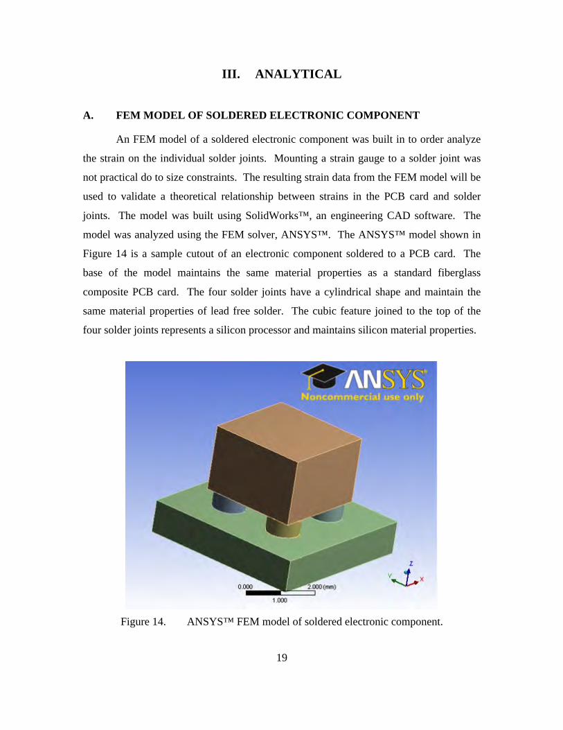
A. FEM MODEL OF SOLDERED ELECTRONIC COMPONENT
An FEM model of a soldered electronic component was built in to order analyze
the strain on the individual solder joints. Mounting a strain gauge to a solder joint was
not practical do to size constraints. The resulting strain data from the FEM model will be
used to validate a theoretical relationship between strains in the PCB card and solder
joints. The model was built using SolidWorks™, an engineering CAD software. The
model was analyzed using the FEM solver, ANSYS™. The ANSYS™ model shown in
Figure 14 is a sample cutout of an electronic component soldered to a PCB card. The
base of the model maintains the same material properties as a standard fiberglass
composite PCB card. The four solder joints have a cylindrical shape and maintain the
same material properties of lead free solder. The cubic feature joined to the top of the
four solder joints represents a silicon processor and maintains silicon material properties.
Figure 14. ANSYS™ FEM model of soldered electronic component.
20
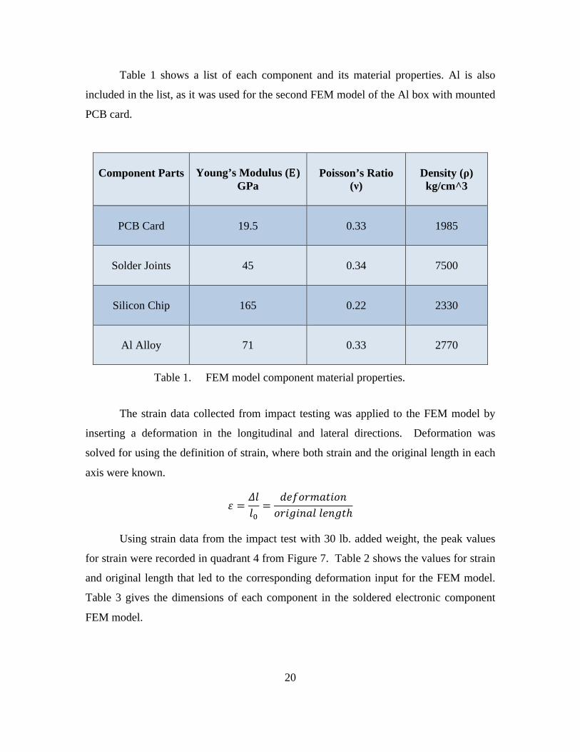
Table 1 shows a list of each component and its material properties. Al is also
included in the list, as it was used for the second FEM model of the Al box with mounted
PCB card.
Component Parts
Young’s Modulus (E) GPa
Poisson’s Ratio
(ν)
Density (ρ) kg/cm^3
PCB Card
19.5
0.33
1985
Solder Joints
45
0.34
7500
Silicon Chip
165
0.22
2330
Al Alloy
71
0.33
2770
Table 1. FEM model component material properties.
The strain data collected from impact testing was applied to the FEM model by
inserting a deformation in the longitudinal and lateral directions. Deformation was
solved for using the definition of strain, where both strain and the original length in each
axis were known.
𝜀 =𝛥𝑙𝑙!=
𝑑𝑒𝑓𝑜𝑟𝑚𝑎𝑡𝑖𝑜𝑛𝑜𝑟𝑖𝑔𝑖𝑛𝑎𝑙 𝑙𝑒𝑛𝑔𝑡ℎ
Using strain data from the impact test with 30 lb. added weight, the peak values
for strain were recorded in quadrant 4 from Figure 7. Table 2 shows the values for strain
and original length that led to the corresponding deformation input for the FEM model.
Table 3 gives the dimensions of each component in the soldered electronic component
FEM model.

21
Axis
Strain (µε) mm/mm
Original length (𝒍𝟎)
mm
Deformation (Δl) mm
Longitudinal
11.6
5.0
5.8e-5
Lateral
1.12
5.0
5.6e-6
Table 2. FEM model deformation inputs.
Component
Length (l) mm
Width (w)
mm
Height (h)
mm
Diameter (d) mm
PCB Card
5.0
5.0 1.0
-
Solder Joints
-
- 0.5
1.0
Silicon Chip
3.0
3.0 2.0
-
Table 3. FEM model dimensions.
B. FEM MODEL OF BOX WITH MOUNTED PCB CARD
The second model built in SolidWorks™ was a full-scale version of the Al box,
Al bracket and mounted PCB card. Figure 15 is a wire frame picture of the model in
SolidWorks™ prior to analysis in ANSYS™. This view clearly shows the orientation
and location of the Al bracket mounted inside the Al box. Figure 16 is a picture of the
model following the strain analysis in ANSYS™.
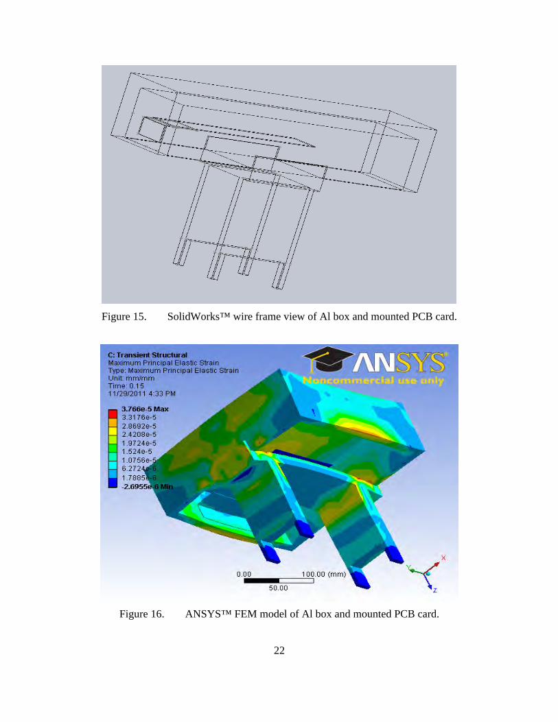
22
Figure 15. SolidWorks™ wire frame view of Al box and mounted PCB card.
Figure 16. ANSYS™ FEM model of Al box and mounted PCB card.

23
The Al Box with mounted PCB card model was designed to exact specifications
and dimensions as the Al box and PCB card used in the experimental impact testing.
Table 4 shows the dimensions for both the Al box and the PCB card.
Component
Length (l) cm
Width (w)
cm
Thickness (t)
cm
Al Box Top
27.9
27.9 1.9
Al Box Sides
27.9
7.6 1.3
PCB Card
15.2
12.7 0.1
Table 4. Al box and PCB card dimensions.
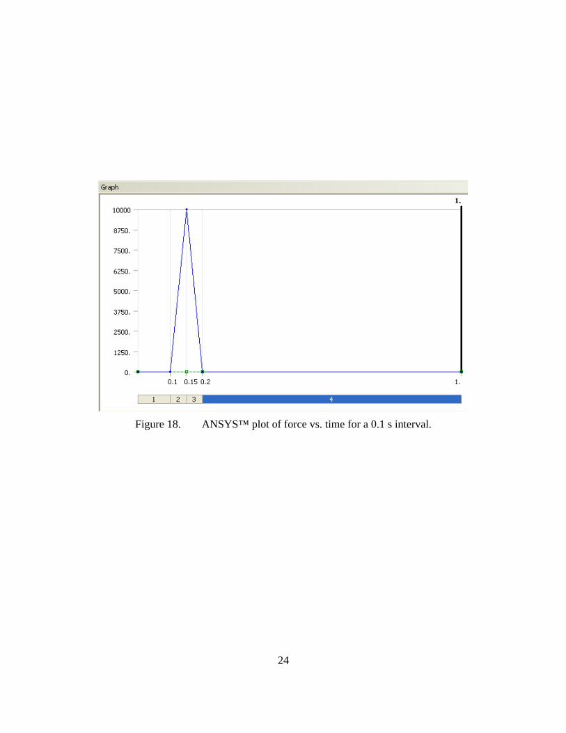
Fixed conditions were applied to the vertical mounting brackets extending down
from the Al box. A vertical impact force of 10 kN was applied to the top of the Al box.
The total test interval was set to 0.1 s. The impact was simulated by turning on and off
the force over a 0.01 s interval. Force data was input into a table within ANSYS™ as
shown in Figure 17. These data point were then plotted as a function of time. Figure 18
is a plot in ANSYS™ of the impact force as a function of time. The number 1 at the far
right hand side of the graph represents 0.1 s and the end of the test interval. The graph
shows the impulse turn on at 0.1, peak at 0.15, and return to zero at 0.2.
Figure 17. ANSYS™ tabular data input.
24
Figure 18. ANSYS™ plot of force vs. time for a 0.1 s interval.

25
IV. RESULTS AND DISCUSSION
A. LONGITUDINAL AND LATERAL STRAIN IN PCB CARD
1. Longitudinal and Lateral Strain as a Function of Time
Seven impact tests were conducted with added weights of 0, 5, 10, 15, 20, 25, and
30 lb. For each impact test, the max values for strain were found in the longitudinal axis
in quadrant 4 from strain gauge number 4. Quadrants 1 and 4 saw higher strain values as
they were closest to the mounted Al bracket. Figures 19 through 25 are plots of both
longitudinal and lateral strain versus time over a period of 0.1 s.

26
Figure 19. Longitudinal and lateral strain with 0 lb. added weight.

27
Figure 20. Longitudinal and lateral strain with 5 lb. added weight.

28
Figure 21. Longitudinal and lateral strain with 10 lb. added weight.

29
Figure 22. Longitudinal and lateral strain with 15 lb. added weight.

30
Figure 23. Longitudinal and lateral strain with 20 lb. added weight.

31
Figure 24. Longitudinal and lateral strain with 25 lb. added weight.

32
Figure 25. Longitudinal and lateral strain with 30 lb. added weight.

33
2. Longitudinal and Lateral Strain as a Function of Added Weight
A second series of plots, Figures 26 through 32, were created in order to show the
maximum longitudinal strain values recorded during each impact test. These values,
recorded in Table 5, were plotted as a function of added weight as shown in Figure 33.
The maximum values for longitudinal strain ranged from 5.04 µε at 0 lb. added weight to
11.60 µε at 30 lb. added weight. The increase in longitudinal strain was roughly linear
over the 0 to 30 lb. range, where the lateral strain remained constant at approximately 1
µε.
Figure 26. Max Longitudinal strain with 0 lb. added weight.

34
Figure 27. Max Longitudinal strain with 5 lb. added weight.
Figure 28. Max Longitudinal strain with 10 lb. added weight.

35
Figure 29. Max Longitudinal strain with 15 lb. added weight.
Figure 30. Max Longitudinal strain with 20 lb. added weight.

36
Figure 31. Max Longitudinal strain with 25 lb. added weight.
Figure 32. Max Longitudinal strain with 30 lb. added weight.

37
Strain (µε)
0 lb. added WT
5 lb.
added WT
10 lb. added WT
15 lb. added WT
20 lb. added WT
25 lb. added WT
30 lb. added WT
Longitudinal
5.04 5.20 7.12 9.00 10.94 11.27 11.60
Lateral
0.80 0.85 0.91 1.12 1.13 0.81 1.06
Table 5. Max Longitudinal and lateral strain values.
Figure 33. Max Longitudinal and lateral strain as a function of added weight.

38
B. FEM ANALYSIS OF SOLDERED ELECTRONIC COMPONENT
The FEM analysis of the soldered electronic component provided both visual and
numerical solder joint strain results. Tables 6 and 7 list the magnitudes of the five
different strains analyzed in ANSYS™. Included in the tables are the maximum values
for normal strain in the longitudinal and lateral axis, as well as the maximum principal
strain for the model. Also found in the tables are max values for shear strain in the XY
and YZ plane and the max shear strain for the model.
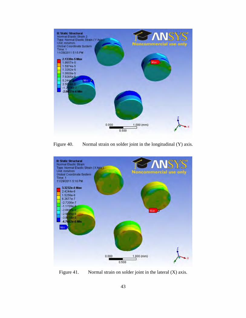
Strain Axis
Normal Strain (µε)
Max Principal Strain
(µε)
Longitudinal
(Y)
21.34
28.15 Lateral
(X)
3.32
Table 6. Max longitudinal, lateral, and principal strain values for the model.
Strain Plane
Shear Strain (µε)
XY
13.19
YZ
40.33
Table 7. Shear in the XY and YZ plane.

39
The ANSYS™ images produced following the analysis of the five strain values
provide a visual reference to the location of the strain. Figures 34 through 43 are color
coded to show the maximum and minimum values for strain. Locations on the model
colored red represent maximum strains, and those locations colored blue represent
minimums. The included legend on the far left hand side of each image represents all
values between the maximums and minimums. Images showing only four cylindrical
solder joints were created by suppressing all other bodies in the model. This allows the
viewer to observe strain characteristics on all surfaces of the solder joint.
Figures 34 through 38 are full model views of the maximum principal, normal,
and shear strains on the soldered electronic component. From top to bottom, the silicon
ship is joined to the PCB card by means of four lead free solder joints.
Figure 34. Max principal strain.

40
Figure 35. Normal strain in the longitudinal (Y) axis.
Figure 36. Normal strain in the lateral (X) axis.

41
Figure 37. Shear strain in the XY plane.
Figure 38. Shear strain in the YZ plane.

42
The maximum values for strain are consistently found at the solder joint and PCB
card interface. Figures 39 through 43 show a suppressed view of the model with only the
four solder joints and their corresponding strains solder joint. These images provide an
unobstructed view of the strains on the PCB card and solder joint interface.
Figure 39. Max principal strain on solder joint.
43
Figure 40. Normal strain on solder joint in the longitudinal (Y) axis.
Figure 41. Normal strain on solder joint in the lateral (X) axis.

44
Figure 42. Shear strain on solder joint in the XY plane.
Figure 43. Shear strain on solder join in the YZ plane.

45
C. FEM ANALYSIS OF BOX WITH MOUNTED PCB CARD
The second FEM model analysis conducted in ANSYS™ was a full-scale version
of the Al box and PCB card used in experimental testing. A 10 kN impact force was used
simulate the experimental impact test using the 30 lb. of added weight. Tables 8 and 9
list the maximum values of strain observed in the ANSYS™ analysis of the PCB card.
The results from ANSYS™ are compared to the values of strain found on the PCB card
from the experimental testing.
Strain Axis
Normal Strain (µε)
Max Principal Strain
(µε)
Longitudinal
(X)
12.5
10.75 Lateral
(Y)
0.75
Table 8. Max longitudinal, lateral, and principal strain values in ANSYS™ PCB card.
Strain Plane
Shear Strain (µε)
Max Shear Strain
(µε)
XY
13.50
22.10 XZ
7.95
Table 9. XY, XZ, and max shear strain values in ANSYS™ PCB card.

46
Table 10 compares the experimental values for both longitudinal and lateral
strains with those found in the ANSYS™ analysis of the PCB card. The difference in
values can be attributed to the approximated 10 kN impact force used in the FEM model.
In addition, the location of the strain gauges in the experimental testing was not identical
to the location of the strains used from the FEM model. Although variations exist, the
error between the ANSYS™ and experimental values of strain in the PCB card are
negligible.
PCB Card
Normal Strain
Longitudinal (µε)
Normal Strain Lateral (µε)
ANSYS™
12.50 0.75
Experimental
11.60 1.06
Table 10. Shear in the XY and YZ plane, and max shear strain for the model.
Figures 44 through 49 depict both a top and bottom view of the 6 different strains
analyzed on the Al box and mounted PCB card. Figures 50 through 55 are top down
views of the PCB card and the six different strains analyzed, with the Al box and Al
bracket suppressed. Each image was captured at the peak of impact force at time step
0.15. Consistent with the experimental impact results, max strain values on the PCB card
were seen closest to the mounting location on the Al bracket.

47
Figure 44. Max principal strain in Al box and PCB card.

48
Figure 45. Normal strain in the longitudinal (X) axis in Al box and PCB card.

49
Figure 46. Normal strain in the lateral (Y) axis in Al box and PCB card.

50
Figure 47. Max shear strain in Al box and PCB card.

51
Figure 48. Shear strain in XY plane on Al box and PCB card.

52
Figure 49. Shear strain in XZ plane on Al box and PCB card.

53
Figure 50. Max principal strain on PCB card.
Figure 51. Normal strain in the longitudinal (X) axis on PCB card.

54
Figure 52. Normal strain in the lateral (Y) axis on PCB card.
Figure 53. Max shear strain on PCB card.

55
Figure 54. Shear strain in XY plane on PCB card.
Figure 55. Shear strain in XZ plane on PCB card.

56
D. STRAIN RELATIONSHIP BETWEEN PCB CARD AND SOLDER JOINT
Establishing a relationship between strains in the PCB card and corresponding
solder joints was a critical objective in this study. A FEM model’s accuracy will greatly
depend on the size or detail of the applied mesh. A very fine mesh can take days or
weeks to solve. Solder joints present a difficult problem in the fact that they are often on
the scale of 1.0 mm or less at their diameter. In the FEM model of the soldered electronic
component, a 5 mm x 5 mm PCB card cutout was use for analysis. This zoomed in view
of the card and component allowed a medium sized mesh to provide accurate results.
The reason this model worked was the minimal size difference between the solder
joints and the PCB card cutout. A very specific location and value for strain were known
from experimental testing, and this allowed a corresponding deformation to be applied at
a precise point on the FEM model. In order to find accurate results using this zoomed in
approach, an additional FEM model would need to be created for every location of
known strain. This method is extremely time intensive and unrealistic in large scale
applications.
The second FEM model of the Al box and the mounted PCB card did not include
any solder joints. Since the model was built to the exact specifications of the
experimental test platform, the size difference between the PCB card and individual
solder joints would have been too great to apply an accurate mesh. Therefore,
establishing a strain relationship would allow this second model to provide PCB card
strain values corresponding potential solder joints in the same location.
A theoretical strain relationship was developed. Figure 56 shows this relationship
between the normal and shear strains in the PCB card and corresponding solder joints.

57
Figure 56. Theoretical relationship between normal and shear strains in PCB cards
and corresponding solder joints.
The solder joint average strain values were collected from the FEM analysis of
the soldered electronic component. Each ANSYS™ image provided a range of strain
values at each solder joint. These values were interpolated and input into the strain
relationships. Table 11 shows the results of this comparison between the theoretical and
the ANSYS™ FEM model of the soldered electronic component. As the results show,
the differences found between the theoretical and ANSYS™ values were very small.
What little error that does exist can be attributed to the average values of strain collected
from the ANSYS™ images. Therefore, the theoretical strain relationships have been
validated by the FEM model, and a relationship has been established between PCB card
and solder joint strain.
• Relationship between PCB and solder joint strains !
εsx!=!!epx ! ! ! ! ! !!
εsy!=!!epy ! ! ! ! ! ! ! !!γsxy!=!!epx+epy ! ! ! ! ! ! !!
γsyz!=!!epy(a/h) ! ! ! ! ! ! !!γsxz!=!!epx(a/h) !!!
s = solder joint p = PCB card a = 1.0 mm (diameter of solder joint) h = 0.5mm (height of solder joint)

58
Analysis Method
𝜺𝒚 (µε)
𝜺𝒙 (µε)
𝜸𝒙𝒚 (µε)
𝜸𝒚𝒛 (µε)
Theoretical
11.40 1.05 12.50 22.80
ANSYS™
12.20 1.06 11.50 22.10
Table 11. Theoretical and ANSYS™ strain comparison.

59
V. CONCLUSIONS AND RECOMMENDATIONS
Testing was conducted in order to analyze the effects of impact loading on
electronic component failure. An existing impact test platform was modified to
incorporate the use of an Al test box. This design and modification allowed for both
impact testing for PCB card strain as well as solder joint failure. Experimental impact
testing for strain revealed an approximately linear relationship between longitudinal
strain and added weight, where lateral strain remained constant throughout. In addition,
analytical results from the FEM model of the soldered electronic component have
verified a valuable theoretical relationship between strain in a PCB card and
corresponding solder joints. Though a failure criteria was not established by means of
experimental impact testing, the FEM model of the Al box and PCB card will allow
improvements and optimizations for future impact study.
The current study may be extended in the following ways:
(i) Further FEM modeling should be conducted to modify existing impact test
apparatus, in order to produce solder joint failure and develop failure criteria.
(ii) Extensive testing should be conducted on various electronic components
and solder joint methods, to include a variation in size and orientation.
(iii) Analyze the effects of underwater impact loading on solder joint failure.

60
THIS PAGE INTENTIONALLY LEFT BLANK

61
LIST OF REFERENCES
[1] M. Celik and C. Genc, “Mechanical fatigue of an electronic component under random vibration,” Fatigue & Fracture of Engineering Materials & Structures, vol. 31, pp. 505–516.
[2] A. Luteran, “Experimental study of solder/copper interface under varying strain
rates,” M.S. thesis, Mech. Eng., Naval Postgraduate School, Monterey, CA, 2011. [3] B. Boyce, L. Brewer, M. Neilsen, and M. Perricone, “On the strain rate and
temperature dependent tensile behavior of eutectic Sn-Pb solder,” ASME Journal of Electronic Packaging, 2011, vol. 133.
[4] H. Pang and X. Che, “Drop impact analysis of sn-ag-cu solder joints using
dynamic high strain rate plastic strain as the impact driving force,” in Electronics Components and Technology Conference, Singapore, 2006, pp. 49–54.
[5] A. Ugural and S. Fenster, Advanced Strength and Applied Elasticity. Upper
Saddle, NJ: Prentice Hall Professional Technical Reference, 2003. [6] A. Owens, “An experimental study of fluid structure interaction of carbon
composites under low velocity impact,” M.S. thesis, Mech. Eng., Naval Postgraduate School, Monterey, CA, 2009.
[7] D. Monniaux. The Pin Grid Array at the Bottom of a Motorola XC68020,
January 2003, http://en.wikipedia.org/wiki/File:XC68020_bottom_p1160085.jpg. Accessed November 5, 2011.
[8] Digi-Key Corporation: IC OMAP DUAL CORE PROC 289-BGA, January 1995,
http://media.digikey.com/Renders/Texas Instr Renders/ZZG-289-BGA Pkg.jpg. Accessed November 5, 2011.
[9] Digi-Key Corporation: BI Technologies 668-A-1002DLF Resistor Pack, January
1995, http://octopart.com/668-a-1002dlf-bi+technologies-2485938. Accessed November 5, 2011.

62
THIS PAGE INTENTIONALLY LEFT BLANK

63
INITIAL DISTRIBUTION LIST
1. Defense Technical Information Center Ft. Belvoir, Virginia
2. Dudley Knox Library Naval Postgraduate School Monterey, California
3. Young W. Kwon Naval Postgraduate School Monterey, California
4. Jarema M. Didoszak Naval Postgraduate School Monterey, California
5. Andrew C. Wood Naval Postgraduate School Monterey, California