ncp4620 - 150 ma, 10 v, low dropout regulator
TRANSCRIPT

© Semiconductor Components Industries, LLC, 2012
May, 2012 − Rev. 41 Publication Order Number:
NCP4620/D
NCP4620
150 mA, 10 V, Low DropoutRegulator
The NCP4620 is a CMOS Linear voltage regulator with 150 mAoutput current capability. The device is capable of operating with inputvoltages up to 10 V, with high output voltage accuracy and lowtemperature−drift coefficient. The NCP4620 is easy to use, withoutput current fold−back protection and a thermal shutdown circuitincluded. A Chip Enable function is included to save power bylowering supply current.
Features• Operating Input Voltage Range: 2.6 V to 10 V
• Output Voltage Range: 1.2 V to 6.0 V (available in 0.1 V steps)
• Output Voltage Accuracy: ±1.0%
• Low Supply Current: 23 �A
• Low Dropout: 165 mV (IOUT = 100 mA, VOUT = 3.3 V) 400 mV (IOUT = 150 mA, VOUT = 2.8 V)
• High PSRR: 70 dB at 1 kHz
• Line Regulation 0.02%/V Typ
• Current Fold Back Protection
• Thermal Shutdown Protection
• Stable with Ceramic Capacitors
• Available in SC−70 and SOT23 Packages
• These are Pb−Free Devices*
Typical Applications• Battery products powered by 2 Lithium Ion cells
• Networking and Communication Equipment
• Cameras, DVRs, STB and Camcorders
• Toys, industrial applications
VIN VOUT
CEGND
C1 C 21� 1�
VIN VOUTNCP4620x
Figure 1. Typical Application Schematic
*For additional information on our Pb−Free strategy and soldering details, pleasedownload the ON Semiconductor Soldering and Mounting TechniquesReference Manual, SOLDERRM/D.
http://onsemi.com
See detailed ordering and shipping information in the packagedimensions section on page 14 of this data sheet.
ORDERING INFORMATION
SC−70CASE 419A
XXXX, XXX= Specific Device CodeMM = Date Code
MARKINGDIAGRAMS
XXXXMM
SOT−23−5CASE 1212 1
XXXMM
1
NCP4620
http://onsemi.com2
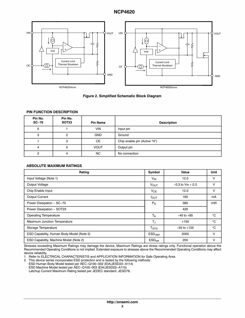
Current LimitThermal Shutdown
VIN
GND
Vref
CE
VOUT
NCP4620Hxxxx
Current LimitThermal Shutdown
VIN
GND
Vref
CE
VOUT
NCP4620Dxxxx
Figure 2. Simplified Schematic Block Diagram
PIN FUNCTION DESCRIPTION
Pin No.SC−70
Pin No.SOT23 Pin Name Description
5 1 VIN Input pin
3 2 GND Ground
1 3 CE Chip enable pin (Active “H”)
4 5 VOUT Output pin
2 4 NC No connection
ABSOLUTE MAXIMUM RATINGS
Rating Symbol Value Unit
Input Voltage (Note 1) VIN 12.0 V
Output Voltage VOUT −0.3 to VIN + 0.3 V
Chip Enable Input VCE 12.0 V
Output Current IOUT 165 mA
Power Dissipation − SC−70 PD 380 mW
Power Dissipation − SOT23 420
Operating Temperature TA −40 to +85 °C
Maximum Junction Temperature TJ +150 °C
Storage Temperature TSTG −55 to +125 °C
ESD Capability, Human Body Model (Note 2) ESDHBM 2000 V
ESD Capability, Machine Model (Note 2) ESDMM 200 V
Stresses exceeding Maximum Ratings may damage the device. Maximum Ratings are stress ratings only. Functional operation above theRecommended Operating Conditions is not implied. Extended exposure to stresses above the Recommended Operating Conditions may affectdevice reliability.1. Refer to ELECTRICAL CHARACTERISTIS and APPLICATION INFORMATION for Safe Operating Area.2. This device series incorporates ESD protection and is tested by the following methods:
ESD Human Body Model tested per AEC−Q100−002 (EIA/JESD22−A114)ESD Machine Model tested per AEC−Q100−003 (EIA/JESD22−A115)Latchup Current Maximum Rating tested per JEDEC standard: JESD78.
NCP4620
http://onsemi.com3
THERMAL CHARACTERISTICS
Rating Symbol Value Unit
Thermal Characteristics, SOT23 Thermal Resistance, Junction−to−Air
R�JA 238 °C/W
Thermal Characteristics, SC−70Thermal Resistance, Junction−to−Air
R�JA 263 °C/W
ELECTRICAL CHARACTERISTICS −40°C ≤ TA ≤ 85°C; VIN = VOUT(NOM) + 1 V; IOUT = 1 mA, CIN = COUT = 0.47 �F, unlessotherwise noted. Typical values are at TA = +25°C.
Parameter Test Conditions Symbol Min Typ Max Unit
Operating Input Voltage VIN 2.6 10 V
Output Voltage TA = +25°C VOUT > 1.5 VVOUT ≤ 1.5 V
VOUT x0.99−15
x1.0115
VmV
−40°C ≤ TA ≤ 85°C VOUT > 1.5 VVOUT ≤ 1.5 V
x0.974−40
x1.02335
VmV
Output Voltage Temp. Coeffi-cient
−40°C ≤ TA ≤ 85°C ±80 ppm/°C
Line Regulation VOUT(NOM) + 0.5 V or 2.6 V (whichever is higher)≤ VIN ≤ 10 V
LineReg 0.02 0.2 %/V
Load Regulation IOUT = 0.1 mA to 150 mA LoadReg 5 40 mV
Dropout Voltage IOUT = 150 mA 1.2 V ≤ VOUT < 1.3 V1.3 V ≤ VOUT < 1.5 V1.5 V ≤ VOUT < 1.8 V1.8 V ≤ VOUT < 2.3 V2.3 V ≤ VOUT < 3.0 V3.0 V ≤ VOUT < 4.0 V4.0 V ≤ VOUT < 6.0 V
VDO
0.400.300.25
1.401.301.100.800.580.480.40
V
Output Current IOUT 150 mA
Short Current Limit VOUT = 0 V ISC 40 mA
Quiescent Current IQ 23 40 �A
Standby Current VIN = 10 V, VCE = 0 V, TA = 25°C ISTB 0.1 1.0 �A
CE Pin Threshold Voltage CE Input Voltage “H” VCEH 1.7 V
CE Input Voltage “L” VCEL 0.8
CE Pull Down Current ICEPD 0.3 �A
Power Supply Rejection Ratio VIN = VOUT + 1 V or 3.0 V whichever is higher,�VIN = 0.2 Vpk−pk, IOUT = 30 mA, f = 1 kHz
PSRR 70 dB
Output Noise Voltage f = 10 Hz to 100 kHz, IOUT = 30 mA, VOUT =1.5 V, VIN = 2.6 V
VN 90 �Vrms
Low Output N−ch Tr. On Resist-ance
VIN = 7 V, VCE = 0 V RLOW 250 �
Thermal Shutdown Temperature TTSD 165 °C
Thermal Shutdown Release TTSR 110 °C
NCP4620
http://onsemi.com4
TYPICAL CHARACTERISTICS
0.0
0.2
0.4
0.6
0.8
1.0
1.2
1.4
1.6
0 50 100 150 200 250IOUT (mA)
VO
UT (
V)
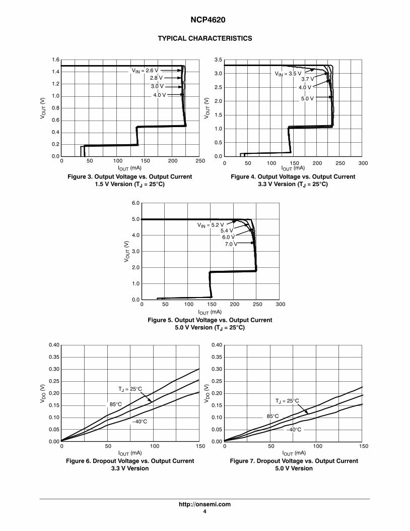
Figure 3. Output Voltage vs. Output Current1.5 V Version (TJ = 25�C)
VIN = 2.6 V2.8 V
4.0 V
3.0 V
0.0
0.5
1.0
1.5
2.0
2.5
3.0
3.5
0 50 100 150 200 250 300IOUT (mA)
Figure 4. Output Voltage vs. Output Current3.3 V Version (TJ = 25�C)
VIN = 3.5 V3.7 V
5.0 V
4.0 V
0.0
1.0
2.0
3.0
4.0
5.0
6.0
0 50 100 150 200 250 300IOUT (mA)
VO
UT (
V)
Figure 5. Output Voltage vs. Output Current5.0 V Version (TJ = 25�C)
VIN = 5.2 V5.4 V
7.0 V6.0 V
VO
UT (
V)
0.00
0.05
0.10
0.15
0.20
0.25
0.30
0.35
0.40
0 50 100 150
VD
O (
V)
IOUT (mA)
Figure 6. Dropout Voltage vs. Output Current3.3 V Version
TJ = 25°C
85°C
−40°C
0.00
0.05
0.10
0.15
0.20
0.25
0.30
0.35
0.40
0 50 100 150IOUT (mA)
Figure 7. Dropout Voltage vs. Output Current5.0 V Version
TJ = 25°C
85°C
−40°C
VD
O (
V)
NCP4620
http://onsemi.com5
TYPICAL CHARACTERISTICS
1.45
1.46
1.47
1.48
1.49
1.50
1.51
1.52
1.53
1.54
1.55
−40 −20 0 20 40 60 80
TJ, JUNCTION TEMPERATURE (°C)
VO
UT (
V)
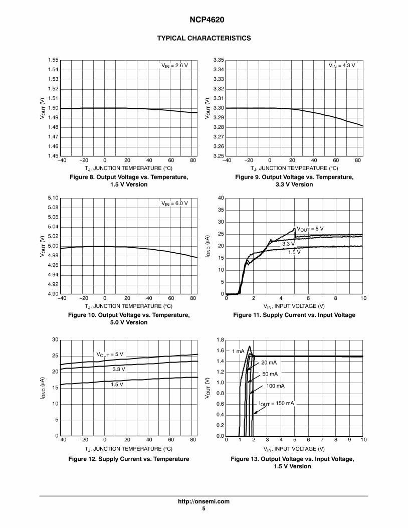
VIN = 2.6 V
Figure 8. Output Voltage vs. Temperature,1.5 V Version
3.25
3.26
3.27
3.28
3.29
3.30
3.31
3.32
3.33
3.34
3.35
TJ, JUNCTION TEMPERATURE (°C)
Figure 9. Output Voltage vs. Temperature,3.3 V Version
VO
UT (
V)
VIN = 4.3 V
−40 −20 0 20 40 60 80
4.90
4.92
4.94
4.96
4.98
5.00
5.02
5.04
5.06
5.08
5.10
−40 −20 0 20 40 60 80
TJ, JUNCTION TEMPERATURE (°C)
VO
UT (
V)
VIN = 6.0 V
Figure 10. Output Voltage vs. Temperature,5.0 V Version
0
5
10
15
20
25
30
35
40
0 2 4 6 8 10
3.3 V
VOUT = 5 V
1.5 V
VIN, INPUT VOLTAGE (V)
I GN
D (�A
)
Figure 11. Supply Current vs. Input Voltage
0
5
10
15
20
25
30
−40 −20 0 20 40 60 80
TJ, JUNCTION TEMPERATURE (°C)
I GN
D (�A
)
Figure 12. Supply Current vs. Temperature
3.3 V
VOUT = 5 V
1.5 V
0.0
0.2
0.4
0.6
0.8
1.0
1.2
1.4
1.6
1.8
0 1 2 3 4 5 6 7 8 9 10
VO
UT (
V)
VIN, INPUT VOLTAGE (V)
IOUT = 150 mA
100 mA
50 mA
20 mA
1 mA
Figure 13. Output Voltage vs. Input Voltage,1.5 V Version

NCP4620
http://onsemi.com6
TYPICAL CHARACTERISTICS
0.0
0.5
1.0
1.5
2.0
2.5
3.0
3.5
0 1 2 3 4 5 6 7 8 9 10
VO
UT (
V)
VIN, INPUT VOLTAGE (V)
IOUT = 150 mA
100 mA
50 mA
20 mA
1 mA
Figure 14. Output Voltage vs. Input Voltage,3.3 V Version
0.0
1.0
2.0
3.0
4.0
5.0
6.0
0 1 2 3 4 5 6 7 8 9 10
VO
UT (
V)
VIN, INPUT VOLTAGE (V)
Figure 15. Output Voltage vs. Input Voltage,5.0 V Version
IOUT = 150 mA
100 mA50 mA
20 mA
1 mA
0
20
40
60
80
100
120
0.01 0.1 1 10 100 1000
Figure 16. PSRR, 1.5 V Version, VIN = 3.5 V
PS
RR
(dB
)
FREQUENCY (kHz)
IOUT = 100 mA
30 mA
1 mA
0
20
40
60
80
100
120
0.01 0.1 1 10 100 1000
PS
RR
(dB
)
Figure 17. PSRR, 3.3 V Version, VIN = 5.3 VFREQUENCY (kHz)
1 mA
30 mA
IOUT = 100 mA
0
20
40
60
80
100
120
0.01 0.1 1 10 100 1000
Figure 18. PSRR, 5.0 V Version, VIN = 7.0 V
PS
RR
(dB
)
FREQUENCY (kHz)
1 mA
30 mA
IOUT = 100 mA
Figure 19. Output Voltage Noise, 1.5 V Version,VIN = 2.6 V, IOUT = 30 mA
0
0.5
1.0
1.5
2.0
2.5
3.0
0.01 0.1 1 10 100 1000
VN
(�V
rms/
√Hz)
FREQUENCY (kHz)

NCP4620
http://onsemi.com7
TYPICAL CHARACTERISTICS
Figure 20. Output Voltage Noise, 3.3 V Version,VIN = 4.3 V, IOUT = 30 mA
VN
(�V
rms/
√Hz)
FREQUENCY (kHz)
Figure 21. Output Voltage Noise, 5.0 V Version,VIN = 6.0 V, IOUT = 30 mA
VN
(�V
rms/
√Hz)
FREQUENCY (kHz)
Figure 22. Line Transients, 1.5 V Version,tR = tF = 5 �s, IOUT = 30 mA
1.47
1.48
1.49
1.50
1.51
0 10 20 30 40 50 60 70 80 90 100
2.5
3.0
3.5
4.0
VO
UT (
V)
t (�s)
VIN
(V
)
Figure 23. Line Transients, 3.3 V Version,tR = tF = 5 �s, IOUT = 30 mA
3.27
3.28
3.29
3.30
0 10 20 30 40 50 60 70 80 90 100
4.3
4.8
5.3
5.8
3.31VO
UT (
V)
t (�s)
VIN
(V
)
10
9.0
8.0
7.0
6.0
5.0
4.0
3.0
2.0
1.0
00.01 0.1 1 10 100 1000 0.01 0.1 1 10 100 1000
25
20
15
10
5
0

NCP4620
http://onsemi.com8
TYPICAL CHARACTERISTICS
Figure 24. Line Transients, 5.0 V version,tR = tF = 5 �s, IOUT = 30 mA
4.97
4.98
4.99
5.00
5.01
0 10 20 30 40 50 60 70 80 90 100
6.0
6.5
7.0
7.5
VO
UT (
V)
t (�s)
VIN
(V
)
Figure 25. Load Transients, 1.5 V Version,IOUT = 50 – 100 mA, tR = tF = 0.5 �s, VIN = 2.6 V
1.42
1.44
1.46
1.48
1.50
1.52
1.54
0 20 40 60 80 100 120 140 160 180 200
0
25
50
75
100
125
VO
UT (
V)
t (�s)
I OU
T (
mA
)
Figure 26. Load Transients, 3.3 V Version,IOUT = 50 – 100 mA, tR = tF = 0.5 �s, VIN = 4.3 V
3.22
3.24
3.26
3.28
3.30
3.32
3.34
3.36
0 20 40 60 80 100 120 140 160 180 200
0
25
50
75
100
125
VO
UT (
V)
t (�s)
I OU
T (
mA
)

NCP4620
http://onsemi.com9
TYPICAL CHARACTERISTICS
Figure 27. Load Transients, 5.0 V Version,IOUT = 50 – 100 mA, tR = tF = 0.5 �s, VIN = 6.0 V
4.80
4.85
4.90
4.95
5.00
5.05
5.10
0 20 40 60 80 100 120 140 160 180 200
0
25
50
75
100
125
VO
UT (
V)
t (�s)
I OU
T (
mA
)
Figure 28. Load Transients, 1.5 V Version,IOUT = 1 – 30 mA, tR = tF = 0.5 �s, VIN = 2.6 V
1.42
1.44
1.46
1.48
1.50
1.52
1.54
0 20 40 60 80 100 120 140 160 180 200
0
15
30
45
VO
UT (
V)
t (�s)
I OU
T (
mA
)
Figure 29. Load Transients, 3.3 V Version,IOUT = 1 – 30 mA, tR = tF = 0.5 �s, VIN = 4.3 V
3.22
3.24
3.26
3.28
3.30
3.32
3.34
0 20 40 60 80 100 120 140 160 180 200
0
15
30
45
VO
UT (
V)
t (�s)
I OU
T (
mA
)
NCP4620
http://onsemi.com10
TYPICAL CHARACTERISTICS
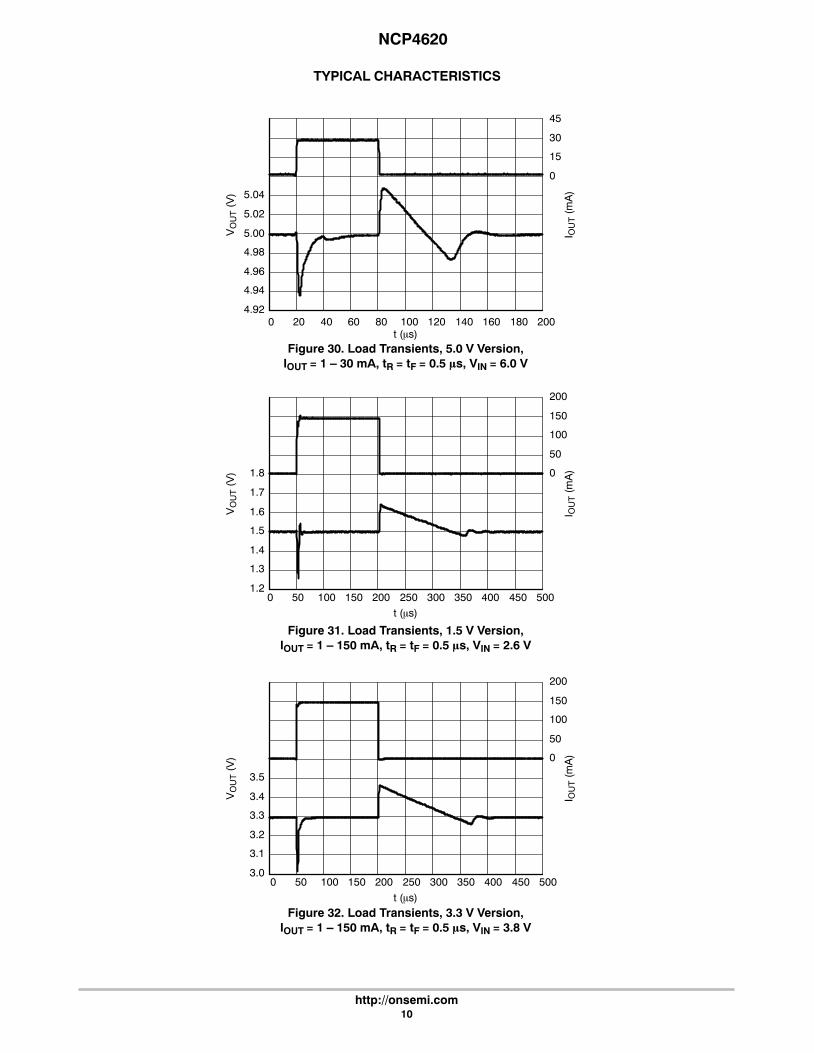
Figure 30. Load Transients, 5.0 V Version,IOUT = 1 – 30 mA, tR = tF = 0.5 �s, VIN = 6.0 V
4.92
4.94
4.96
4.98
5.00
5.02
5.04
0 20 40 60 80 100 120 140 160 180 200
0
15
30
45
VO
UT (
V)
t (�s)
I OU
T (
mA
)
Figure 31. Load Transients, 1.5 V Version,IOUT = 1 – 150 mA, tR = tF = 0.5 �s, VIN = 2.6 V
1.2
1.3
1.4
1.5
1.6
1.7
1.8
0 50 100 150 200 250 300 350 400 450 500
0
50
100
150
200
VO
UT (
V)
t (�s)
I OU
T (
mA
)
Figure 32. Load Transients, 3.3 V Version,IOUT = 1 – 150 mA, tR = tF = 0.5 �s, VIN = 3.8 V
3.0
3.1
3.2
3.3
3.4
3.5
0 50 100 150 200 250 300 350 400 450 500
0
50
100
150
200
VO
UT (
V)
t (�s)
I OU
T (
mA
)

NCP4620
http://onsemi.com11
TYPICAL CHARACTERISTICS
Figure 33. Load Transients, 5.0 V Version,IOUT = 1 – 150 mA, tR = tF = 0.5 �s, VIN = 6.0 V
4.4
4.6
4.8
5.0
5.2
5.4
5.6
0 50 100 150 200 250 300 350 400 450 500
0
50
100
150
200
VO
UT (
V)
I OU
T (
mA
)
t (�s)
Figure 34. Start−up, 1.5 V Version, VIN = 2.6 V
−0.5
0
0.5
1.0
1.5
2.0
0 20 40 60 80 100 120 140 160 180 200
0
1
2
3
VO
UT (
V)
t (�s)
VC
E (
V)
Chip Enable
IOUT = 150 mA
IOUT = 30 mA
IOUT = 1 mA
Figure 35. Start−up, 3.3 V Version, VIN = 4.3 V
−1.0
0
1.0
2.0
3.0
4.0
0 20 40 60 80 100 120 140 160 180 200
0
2
4
6
VO
UT (
V)
t (�s)
VC
E (
V)
Chip Enable
IOUT = 150 mA
IOUT = 30 mA
IOUT = 1 mA

NCP4620
http://onsemi.com12
TYPICAL CHARACTERISTICS
Figure 36. Start−up, 5.0 V Version, VIN = 6.0 V
−1.0
0
1.0
2.0
3.0
4.0
0 20 40 60 80 100 120 140 160 180 200
0
3
6
9
VO
UT (
V)
t (�s)
VC
E (
V)
Chip Enable
IOUT = 150 mA
IOUT = 30 mA
IOUT = 1 mA
Figure 37. Shutdown, 3.3 V Version D,VIN = 4.3 V
−1.0
0
1.0
2.0
3.0
4.0
0 200 400 600 800 1000 1200 1400 1600 1800 2000
0
2
4
6
VO
UT (
V)
t (�s)
VC
E (
V)
Chip Enable
IOUT = 150 mA
IOUT = 30 mA
IOUT = 1 mA
NCP4620
http://onsemi.com13
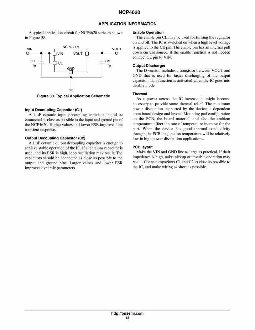
APPLICATION INFORMATION
A typical application circuit for NCP4620 series is shownin Figure 38.
VIN VOUT
CE
GND
C1 C21� 1�
VIN VOUTNCP4620x
Figure 38. Typical Application Schematic
Input Decoupling Capacitor (C1)A 1 �F ceramic input decoupling capacitor should be
connected as close as possible to the input and ground pin ofthe NCP4620. Higher values and lower ESR improves linetransient response.
Output Decoupling Capacitor (C2)A 1 �F ceramic output decoupling capacitor is enough to
achieve stable operation of the IC. If a tantalum capacitor isused, and its ESR is high, loop oscillation may result. Thecapacitors should be connected as close as possible to theoutput and ground pins. Larger values and lower ESRimproves dynamic parameters.
Enable OperationThe enable pin CE may be used for turning the regulator
on and off. The IC is switched on when a high level voltageis applied to the CE pin. The enable pin has an internal pulldown current source. If the enable function is not neededconnect CE pin to VIN.
Output DischargerThe D version includes a transistor between VOUT and
GND that is used for faster discharging of the outputcapacitor. This function is activated when the IC goes intodisable mode.
ThermalAs a power across the IC increase, it might become
necessary to provide some thermal relief. The maximumpower dissipation supported by the device is dependentupon board design and layout. Mounting pad configurationon the PCB, the board material, and also the ambienttemperature affect the rate of temperature increase for thepart. When the device has good thermal conductivitythrough the PCB the junction temperature will be relativelylow in high power dissipation applications.
PCB layoutMake the VIN and GND line as large as practical. If their
impedance is high, noise pickup or unstable operation mayresult. Connect capacitors C1 and C2 as close as possible tothe IC, and make wiring as short as possible.
NCP4620
http://onsemi.com14
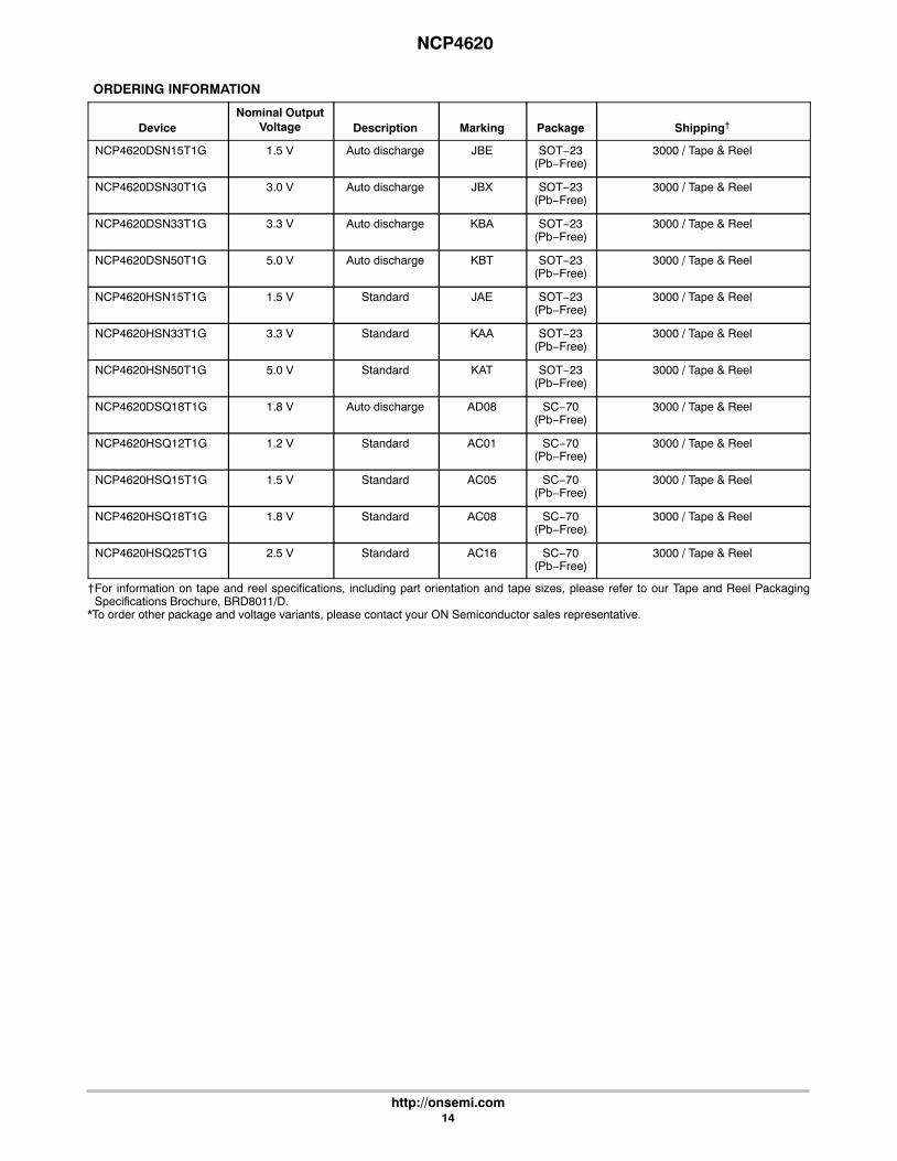
ORDERING INFORMATION
DeviceNominal Output
Voltage Description Marking Package Shipping†
NCP4620DSN15T1G 1.5 V Auto discharge JBE SOT−23(Pb−Free)
3000 / Tape & Reel
NCP4620DSN30T1G 3.0 V Auto discharge JBX SOT−23(Pb−Free)
3000 / Tape & Reel
NCP4620DSN33T1G 3.3 V Auto discharge KBA SOT−23(Pb−Free)
3000 / Tape & Reel
NCP4620DSN50T1G 5.0 V Auto discharge KBT SOT−23(Pb−Free)
3000 / Tape & Reel
NCP4620HSN15T1G 1.5 V Standard JAE SOT−23(Pb−Free)
3000 / Tape & Reel
NCP4620HSN33T1G 3.3 V Standard KAA SOT−23(Pb−Free)
3000 / Tape & Reel
NCP4620HSN50T1G 5.0 V Standard KAT SOT−23(Pb−Free)
3000 / Tape & Reel
NCP4620DSQ18T1G 1.8 V Auto discharge AD08 SC−70(Pb−Free)
3000 / Tape & Reel
NCP4620HSQ12T1G 1.2 V Standard AC01 SC−70(Pb−Free)
3000 / Tape & Reel
NCP4620HSQ15T1G 1.5 V Standard AC05 SC−70(Pb−Free)
3000 / Tape & Reel
NCP4620HSQ18T1G 1.8 V Standard AC08 SC−70(Pb−Free)
3000 / Tape & Reel
NCP4620HSQ25T1G 2.5 V Standard AC16 SC−70(Pb−Free)
3000 / Tape & Reel
†For information on tape and reel specifications, including part orientation and tape sizes, please refer to our Tape and Reel PackagingSpecifications Brochure, BRD8011/D.
*To order other package and voltage variants, please contact your ON Semiconductor sales representative.

SOT−23 5−LEADCASE 1212−01
ISSUE ADATE 28 JAN 2011
DIM MIN MAXMILLIMETERS
A1 0.00 0.10A2 1.00 1.30b 0.30 0.50c 0.10 0.25D 2.70 3.10E 2.50 3.10E1 1.50 1.80e 0.95 BSCLL1 0.45 0.75
NOTES:1. DIMENSIONING AND TOLERANCING PER
ASME Y14.5M, 1994.2. CONTROLLING DIMENSIONS: MILLIMETERS.3. DATUM C IS THE SEATING PLANE.
A
1
5
2 3
4
D
E1
B
L1
E
e CM0.10 C SB SAb5X
A2A1S0.05
C
L
0.20 ---
SCALE 2:1
GENERICMARKING DIAGRAM*
XXX = Specific Device CodeM = Date Code� = Pb−Free Package
*For additional information on our Pb−Free strategy and solderingdetails, please download the ON Semiconductor Soldering andMounting Techniques Reference Manual, SOLDERRM/D.
SOLDERING FOOTPRINT*
*This information is generic. Please refer todevice data sheet for actual part marking.Pb−Free indicator, “G” or microdot “ �”,may or may not be present.
0.95
DIMENSIONS: MILLIMETERS
PITCH
5X3.30
0.565X
0.85
XXX M�
�
A --- 1.45
RECOMMENDED
A
(Note: Microdot may be in either location)
MECHANICAL CASE OUTLINE
PACKAGE DIMENSIONS
ON Semiconductor and are trademarks of Semiconductor Components Industries, LLC dba ON Semiconductor or its subsidiaries in the United States and/or other countries.ON Semiconductor reserves the right to make changes without further notice to any products herein. ON Semiconductor makes no warranty, representation or guarantee regardingthe suitability of its products for any particular purpose, nor does ON Semiconductor assume any liability arising out of the application or use of any product or circuit, and specificallydisclaims any and all liability, including without limitation special, consequential or incidental damages. ON Semiconductor does not convey any license under its patent rights nor therights of others.
98ASH70518ADOCUMENT NUMBER:
DESCRIPTION:
Electronic versions are uncontrolled except when accessed directly from the Document Repository.Printed versions are uncontrolled except when stamped “CONTROLLED COPY” in red.
PAGE 1 OF 1SOT−23 5−LEAD
© Semiconductor Components Industries, LLC, 2019 www.onsemi.com

NOTES:1. DIMENSIONING AND TOLERANCING
PER ANSI Y14.5M, 1982.2. CONTROLLING DIMENSION: INCH.3. 419A−01 OBSOLETE. NEW STANDARD
419A−02.4. DIMENSIONS A AND B DO NOT INCLUDE
MOLD FLASH, PROTRUSIONS, OR GATEBURRS.
DIMA
MIN MAX MIN MAXMILLIMETERS
1.80 2.200.071 0.087
INCHES
B 1.15 1.350.045 0.053C 0.80 1.100.031 0.043D 0.10 0.300.004 0.012G 0.65 BSC0.026 BSCH --- 0.10---0.004J 0.10 0.250.004 0.010K 0.10 0.300.004 0.012N 0.20 REF0.008 REFS 2.00 2.200.079 0.087
STYLE 1:PIN 1. BASE
2. EMITTER 3. BASE 4. COLLECTOR 5. COLLECTOR
STYLE 2:PIN 1. ANODE
2. EMITTER 3. BASE 4. COLLECTOR 5. CATHODE
B0.2 (0.008) M M
1 2 3
45
A
G
S
D 5 PL
H
C
N
J
K
−B−
STYLE 3:PIN 1. ANODE 1
2. N/C 3. ANODE 2 4. CATHODE 2 5. CATHODE 1
STYLE 4:PIN 1. SOURCE 1
2. DRAIN 1/2 3. SOURCE 1 4. GATE 1 5. GATE 2
STYLE 5:PIN 1. CATHODE
2. COMMON ANODE 3. CATHODE 2 4. CATHODE 3 5. CATHODE 4
STYLE 7:PIN 1. BASE
2. EMITTER 3. BASE 4. COLLECTOR 5. COLLECTOR
STYLE 6:PIN 1. EMITTER 2
2. BASE 2 3. EMITTER 1 4. COLLECTOR 5. COLLECTOR 2/BASE 1
XXXM�
�
XXX = Specific Device CodeM = Date Code� = Pb−Free Package
GENERIC MARKINGDIAGRAM*
STYLE 8:PIN 1. CATHODE
2. COLLECTOR 3. N/C 4. BASE 5. EMITTER
STYLE 9:PIN 1. ANODE
2. CATHODE 3. ANODE 4. ANODE 5. ANODE
Note: Please refer to datasheet forstyle callout. If style type is not calledout in the datasheet refer to the devicedatasheet pinout or pin assignment.
SC−88A (SC−70−5/SOT−353)CASE 419A−02
ISSUE LDATE 17 JAN 2013SCALE 2:1
(Note: Microdot may be in either location)
� mminches
�SCALE 20:1
0.650.025
0.650.025
0.500.0197
0.400.0157
1.90.0748
SOLDER FOOTPRINT
*This information is generic. Please refer todevice data sheet for actual part marking.Pb−Free indicator, “G” or microdot “�”, mayor may not be present. Some products maynot follow the Generic Marking.
MECHANICAL CASE OUTLINE
PACKAGE DIMENSIONS
ON Semiconductor and are trademarks of Semiconductor Components Industries, LLC dba ON Semiconductor or its subsidiaries in the United States and/or other countries.ON Semiconductor reserves the right to make changes without further notice to any products herein. ON Semiconductor makes no warranty, representation or guarantee regardingthe suitability of its products for any particular purpose, nor does ON Semiconductor assume any liability arising out of the application or use of any product or circuit, and specificallydisclaims any and all liability, including without limitation special, consequential or incidental damages. ON Semiconductor does not convey any license under its patent rights nor therights of others.
98ASB42984BDOCUMENT NUMBER:
DESCRIPTION:
Electronic versions are uncontrolled except when accessed directly from the Document Repository.Printed versions are uncontrolled except when stamped “CONTROLLED COPY” in red.
PAGE 1 OF 1SC−88A (SC−70−5/SOT−353)
© Semiconductor Components Industries, LLC, 2018 www.onsemi.com

onsemi, , and other names, marks, and brands are registered and/or common law trademarks of Semiconductor Components Industries, LLC dba “onsemi” or its affiliatesand/or subsidiaries in the United States and/or other countries. onsemi owns the rights to a number of patents, trademarks, copyrights, trade secrets, and other intellectual property.A listing of onsemi’s product/patent coverage may be accessed at www.onsemi.com/site/pdf/Patent−Marking.pdf. onsemi reserves the right to make changes at any time to anyproducts or information herein, without notice. The information herein is provided “as−is” and onsemi makes no warranty, representation or guarantee regarding the accuracy of theinformation, product features, availability, functionality, or suitability of its products for any particular purpose, nor does onsemi assume any liability arising out of the application or useof any product or circuit, and specifically disclaims any and all liability, including without limitation special, consequential or incidental damages. Buyer is responsible for its productsand applications using onsemi products, including compliance with all laws, regulations and safety requirements or standards, regardless of any support or applications informationprovided by onsemi. “Typical” parameters which may be provided in onsemi data sheets and/or specifications can and do vary in different applications and actual performance mayvary over time. All operating parameters, including “Typicals” must be validated for each customer application by customer’s technical experts. onsemi does not convey any licenseunder any of its intellectual property rights nor the rights of others. onsemi products are not designed, intended, or authorized for use as a critical component in life support systemsor any FDA Class 3 medical devices or medical devices with a same or similar classification in a foreign jurisdiction or any devices intended for implantation in the human body. ShouldBuyer purchase or use onsemi products for any such unintended or unauthorized application, Buyer shall indemnify and hold onsemi and its officers, employees, subsidiaries, affiliates,and distributors harmless against all claims, costs, damages, and expenses, and reasonable attorney fees arising out of, directly or indirectly, any claim of personal injury or deathassociated with such unintended or unauthorized use, even if such claim alleges that onsemi was negligent regarding the design or manufacture of the part. onsemi is an EqualOpportunity/Affirmative Action Employer. This literature is subject to all applicable copyright laws and is not for resale in any manner.
PUBLICATION ORDERING INFORMATIONTECHNICAL SUPPORTNorth American Technical Support:Voice Mail: 1 800−282−9855 Toll Free USA/CanadaPhone: 011 421 33 790 2910
LITERATURE FULFILLMENT:Email Requests to: [email protected]
onsemi Website: www.onsemi.com
Europe, Middle East and Africa Technical Support:Phone: 00421 33 790 2910For additional information, please contact your local Sales Representative
◊