ncv7471 - system basis chip with a high-speed can, two
TRANSCRIPT

© Semiconductor Components Industries, LLC, 2015
April, 2018 − Rev. 51 Publication Order Number:
NCV7471/D
NCV7471, NCV7471A
System Basis Chip with aHigh-Speed CAN, Two LINsand a Boost-Buck DC/DCConverter
NCV7471(A) is a System Basis Chip (SBC) integrating functionstypically found in automotive Electronic Control Units (ECUs) in thebody domain. NCV7471 provides and monitors the low−voltagepower supplies for the application microcontroller and other loads,monitors the application software via a watchdog and includeshigh−speed CAN and LIN transceivers allowing the ECU to hostmultiple communication nodes or to act as a gateway unit. Theon−chip state controller ensures safe power−up sequence and supportslow−power modes with a configurable set of features includingwakeup from the communication buses or by a local digital signalWU. The status of several NCV7471(A) internal blocks can be read bythe microcontroller through the serial peripheral interface or can beused to generate an interrupt request.
Features• Control Logic
♦ Ensures safe power−up sequence and the correct reaction todifferent supply conditions
♦ Controls mode transitions including the power management andwakeup treatment − bus wakeups, local wakeups (via WU pin) andcyclic wakeups (through the on−chip timer)
♦ Generates reset and interrupt requests• Serial Peripheral Interface
♦ Operates with 16−bit frames♦ Ensures communication with the ECU’s microcontroller unit♦ Mode settings, chip status feedback and watchdog are accessible
through eight twelve−bits registers• 5 V VOUT Supply from a DC/DC Converter
♦ Can deliver up to 500 mA with accuracy of ±2%♦ Supplies typically the ECU’s microcontroller
• 5 V VOUT2 Low−drop Output Regulator♦ Can supply external loads – e.g. sensors♦ Controlled by SPI and the state machine♦ Protected against short to the car battery
• A High−speed CAN Transceiver♦ ISO11898−2 and ISO11898−5 compliant♦ Communication speed up to 1 Mbps♦ TxD dominant time−out protection
• Two LIN Transceivers♦ LIN2.X and J2602 compliant♦ TxD dominant time−out protection
• Wakeup Input WU♦ Edge−sensitive high−voltage input
♦ Can be used as a wake−up source or as a logicalinput polled through SPI
• Protection and Monitoring Functions♦ Monitoring of the main supply through the V_MID
point♦ Monitoring of VOUT supply output with
programmable threshold♦ VOUT2 supply diagnosis through SPI and interrupt♦ Thermal warning and thermal shutdown protection♦ Programmable watchdog monitoring the ECU
software• NCV Prefix for Automotive and Other Applications
Requiring Unique Site and Control ChangeRequirements; AEC−Q100 Qualified and PPAPCapable
• These Devices are Pb−Free, Halogen Free/BFR Freeand are RoHS Compliant
www.onsemi.com
SSOP36−EPDQ SUFFIX
CASE 940AB
MARKING DIAGRAM
XXXXAWLYYWW�
�
XXXX = NCV7471−5 or NCV7471A−5A = Assembly LocationWL = Wafer LotYY = YearWW = Work Week� = Pb−Free Package
See detailed ordering and shipping information on page 49 ofthis data sheet.
ORDERING INFORMATION
(Note: Microdot may be in either location)

NCV7471, NCV7471A
www.onsemi.com2
Pin Connections
V_MIDBOOSTCFGFSO1FSO2FSO3GND_SMPSWUVSVS_VOUT2GNDCANHCANLTEST/GNDLIN1GNDLIN2SWDM
1
18 19
36RSTNINTN
UVN_VOUTSDI
SCKSDOCSN
BUCKGND_SENSE
VOUTVCC_CAN
VOUT2TxDCRxDCTxDL1RxDL1TxDL2RxDL2
Table of ContentsBlock Diagram 3. . . . . . . . . . . . . . . . . . . . . . . . . . . . . . . . . . . . . . . . . . . . . . . . . . . . . . . . . . . . . . . . . . . . . . . . . . . . . . . . . . . . . . . . . . . . . .Pin Description 4. . . . . . . . . . . . . . . . . . . . . . . . . . . . . . . . . . . . . . . . . . . . . . . . . . . . . . . . . . . . . . . . . . . . . . . . . . . . . . . . . . . . . . . . . . . . . .Application Information 5. . . . . . . . . . . . . . . . . . . . . . . . . . . . . . . . . . . . . . . . . . . . . . . . . . . . . . . . . . . . . . . . . . . . . . . . . . . . . . . . . . . . . . .Example Application Diagram 5. . . . . . . . . . . . . . . . . . . . . . . . . . . . . . . . . . . . . . . . . . . . . . . . . . . . . . . . . . . . . . . . . . . . . . . . . . . . . . . . . .External Components 6. . . . . . . . . . . . . . . . . . . . . . . . . . . . . . . . . . . . . . . . . . . . . . . . . . . . . . . . . . . . . . . . . . . . . . . . . . . . . . . . . . . . . . . . .Functional Description 7. . . . . . . . . . . . . . . . . . . . . . . . . . . . . . . . . . . . . . . . . . . . . . . . . . . . . . . . . . . . . . . . . . . . . . . . . . . . . . . . . . . . . . . .Power Supplies 7. . . . . . . . . . . . . . . . . . . . . . . . . . . . . . . . . . . . . . . . . . . . . . . . . . . . . . . . . . . . . . . . . . . . . . . . . . . . . . . . . . . . . . . . . . . . . .Communication Transceivers 10. . . . . . . . . . . . . . . . . . . . . . . . . . . . . . . . . . . . . . . . . . . . . . . . . . . . . . . . . . . . . . . . . . . . . . . . . . . . . . . . . .WU – Local Wakeup Input 14. . . . . . . . . . . . . . . . . . . . . . . . . . . . . . . . . . . . . . . . . . . . . . . . . . . . . . . . . . . . . . . . . . . . . . . . . . . . . . . . . . .Operating Modes 15. . . . . . . . . . . . . . . . . . . . . . . . . . . . . . . . . . . . . . . . . . . . . . . . . . . . . . . . . . . . . . . . . . . . . . . . . . . . . . . . . . . . . . . . . . .Watchdog 19. . . . . . . . . . . . . . . . . . . . . . . . . . . . . . . . . . . . . . . . . . . . . . . . . . . . . . . . . . . . . . . . . . . . . . . . . . . . . . . . . . . . . . . . . . . . . . . . .System Reset 21. . . . . . . . . . . . . . . . . . . . . . . . . . . . . . . . . . . . . . . . . . . . . . . . . . . . . . . . . . . . . . . . . . . . . . . . . . . . . . . . . . . . . . . . . . . . . .Event Flags and Interrupt Requests 22. . . . . . . . . . . . . . . . . . . . . . . . . . . . . . . . . . . . . . . . . . . . . . . . . . . . . . . . . . . . . . . . . . . . . . . . . . . . .Junction Temperature Monitoring 25. . . . . . . . . . . . . . . . . . . . . . . . . . . . . . . . . . . . . . . . . . . . . . . . . . . . . . . . . . . . . . . . . . . . . . . . . . . . . .FSO1/2/3 – Fail-Safe Outputs 25. . . . . . . . . . . . . . . . . . . . . . . . . . . . . . . . . . . . . . . . . . . . . . . . . . . . . . . . . . . . . . . . . . . . . . . . . . . . . . . . .SWDM and CFG Digital Inputs 27. . . . . . . . . . . . . . . . . . . . . . . . . . . . . . . . . . . . . . . . . . . . . . . . . . . . . . . . . . . . . . . . . . . . . . . . . . . . . . . .SPI – Serial Peripheral Interface 28. . . . . . . . . . . . . . . . . . . . . . . . . . . . . . . . . . . . . . . . . . . . . . . . . . . . . . . . . . . . . . . . . . . . . . . . . . . . . . .Absolute Maximum Ratings 38. . . . . . . . . . . . . . . . . . . . . . . . . . . . . . . . . . . . . . . . . . . . . . . . . . . . . . . . . . . . . . . . . . . . . . . . . . . . . . . . . .Operating Ranges 39. . . . . . . . . . . . . . . . . . . . . . . . . . . . . . . . . . . . . . . . . . . . . . . . . . . . . . . . . . . . . . . . . . . . . . . . . . . . . . . . . . . . . . . . . . .Electrical Characteristics 40. . . . . . . . . . . . . . . . . . . . . . . . . . . . . . . . . . . . . . . . . . . . . . . . . . . . . . . . . . . . . . . . . . . . . . . . . . . . . . . . . . . . .Power Supply 40. . . . . . . . . . . . . . . . . . . . . . . . . . . . . . . . . . . . . . . . . . . . . . . . . . . . . . . . . . . . . . . . . . . . . . . . . . . . . . . . . . . . . . . . . . . . . .CAN Transceiver 43. . . . . . . . . . . . . . . . . . . . . . . . . . . . . . . . . . . . . . . . . . . . . . . . . . . . . . . . . . . . . . . . . . . . . . . . . . . . . . . . . . . . . . . . . . .LIN Transceivers 45. . . . . . . . . . . . . . . . . . . . . . . . . . . . . . . . . . . . . . . . . . . . . . . . . . . . . . . . . . . . . . . . . . . . . . . . . . . . . . . . . . . . . . . . . . .Digital Control Timing and SPI Timing 47. . . . . . . . . . . . . . . . . . . . . . . . . . . . . . . . . . . . . . . . . . . . . . . . . . . . . . . . . . . . . . . . . . . . . . . . . .Thermal Protection 48. . . . . . . . . . . . . . . . . . . . . . . . . . . . . . . . . . . . . . . . . . . . . . . . . . . . . . . . . . . . . . . . . . . . . . . . . . . . . . . . . . . . . . . . . .Digital IO Pins 48. . . . . . . . . . . . . . . . . . . . . . . . . . . . . . . . . . . . . . . . . . . . . . . . . . . . . . . . . . . . . . . . . . . . . . . . . . . . . . . . . . . . . . . . . . . . .CFG and SWDM Pins 49. . . . . . . . . . . . . . . . . . . . . . . . . . . . . . . . . . . . . . . . . . . . . . . . . . . . . . . . . . . . . . . . . . . . . . . . . . . . . . . . . . . . . . .FSO Pins 49. . . . . . . . . . . . . . . . . . . . . . . . . . . . . . . . . . . . . . . . . . . . . . . . . . . . . . . . . . . . . . . . . . . . . . . . . . . . . . . . . . . . . . . . . . . . . . . . .WU Pin 49. . . . . . . . . . . . . . . . . . . . . . . . . . . . . . . . . . . . . . . . . . . . . . . . . . . . . . . . . . . . . . . . . . . . . . . . . . . . . . . . . . . . . . . . . . . . . . . . . . .Device Ordering information 49. . . . . . . . . . . . . . . . . . . . . . . . . . . . . . . . . . . . . . . . . . . . . . . . . . . . . . . . . . . . . . . . . . . . . . . . . . . . . . . . . .

NCV7471, NCV7471A
www.onsemi.com3
Figure 1. Block Diagram
CAN transceiver
LIN transceiver
LIN transceiver
TxDC
RxDC
TxDL1
RxDL1
TxDL2
RxDL2
RSTN
INTN
SDI
SDO
SCK
CSN
FSO
FSO
FSO
FSO1
FSO2
FSO3
LIN1
LIN2
CANH
CANL
SWDM
CFG
CONTROL
DC/DC CONVERTER
VOUT2LDO50 mA
VCC_CAN
GND
WU
NCV7471(A)
BOOST
GND_SMPS
VS_VOUT2
Supply monitoringAuxiliary blocks
VS
V_MID BUCK VOUT
UVN_VOUT
GND_SENSE
TEST/GND

NCV7471, NCV7471A
www.onsemi.com4
Table 1. PIN DESCRIPTION
PinNumber Pin Name
Pin Type(LV = Low Voltage; HV = High Voltage) Pin Function
1 RSTN LV digital input/output; open drain;internal pull−up
System reset
2 INTN LV digital output; open drain; internal pull−up Interrupt request to the MCU
3 UVN_VOUT VOUT under−voltage signal to the MCU
4 SDI LV digital input; internal pull−down SPI data input
5 SCK LV digital input; internal pull−down SPI clock input
6 SDO LV digital output; push−pull with tri−state SPI data output
7 CSN LV digital input (HV tolerant); internal pull−up SPI chip select input
8 BUCK HV analog input/output Connection of Lbuck coil to the integrated serial switch
9 GND_SENSE Ground connection Ground sense for the internal circuitry (e.g. VOUT2 regulator)
10 VOUT LV supply input Feedback of the DC/DC converter output; main 5 V LVsupply for the digital IO’s
11 VCC_CAN LV supply input Core supply for the CAN transceiver
12 VOUT2 LV supply output Output of the 5 V/50 mA low−drop regulator for external loads
13 TxDC LV digital input; internal pull−up Input of the data to be transmitted on CAN bus
14 RxDC LV digital output; push−pull Output of data received from CAN bus
15 TxDL1 LV digital input; internal pull−up Input of the data to be transmitted from LIN1 bus
16 RxDL1 LV digital output; push−pull Output of data received on LIN1 bus
17 TxDL2 LV digital input; internal pull−up Input of the data to be transmitted from LIN2 bus
18 RxDL2 LV digital output; push−pull Output of data received on LIN2 bus
19 SWDM HV digital input; internal pull−down Input to select the SW Development configuration
20 LIN2 LIN bus interface LIN2 bus line
21 GND Ground connection Ground connection
22 LIN1 LIN bus interface LIN1 bus line
23 TEST/GND LV digital input; internal pull−down Test−mode entry pin for production testing; should begrounded in the application
24 CANL CAN bus interface CANL line of the CAN bus
25 CANH CAN bus interface CANH line of the CAN bus
26 GND Ground connection Ground connection
27 VS_VOUT2 HV supply input Separate line input for the VOUT2 low−drop regulator
28 VS HV supply input Line supply for the battery−related core blocks
29 WU HV digital input Input for monitoring of external contacts
30 GND_SMPS Ground connection Power ground connection for the DC/DC converter
31 FSO3 HV digital output; open drain low−side Indication of a fail−safe event by rectangular signal of 100 Hzwith 20% duty cycle; high−impedant in normal operation
32 FSO2 HV digital output; open drain low−side Indication of a fail−safe event by rectangular signal of 1.25 Hzwith 50% duty cycle; high−impedant in normal operation
33 FSO1 HV digital output; open drain low−side Indication of a fail−safe event by static Low level;high−impedant in normal operation
34 CFG HV digital input; internal pull−down Configuration of fail−safe behavior; in SW Development,CFG enables boost stage operation
35 BOOST HV analog input/output Connection of Lboost coil to the integrated switch to ground.
36 V_MID HV analog input/output Intermediate point connecting the step−up and step−downstages of the DC/DC converter

NCV7471, NCV7471A
www.onsemi.com5
APPLICATION INFORMATION
Figure 2. Example Application Diagram

NCV7471, NCV7471A
www.onsemi.com6
External Components
Overview of external components from application schematic in Figure 2 is given in Table 2 together with their recommendedor required values.
Table 2. EXTERNAL COMPONENTS OVERVIEW
Component Name Description Value Note
Drev Reverse−protection diode parameters application−specific;e.g. 0.5 A / 50 V
Values and types dependon the application needs
and conditions. Guidelinesfor their selection can be
found in the product’sapplication note.
The given examples aresuitable for VOUT loads of
up to 250 mA, and forV_IN above 3.3 V.
Cin Filtering capacitor for the DC/DCconverter input
≥ 1 �F ceramic;e.g. 1 �F / 40 V
Lboost Inductor for the converter boost stage;EMC filtering inductance
recommended range 3.3 �H – 10 �H;e.g. 3.3 �H / 0.77 A,
type B82422H1332+000
D1 Diode for the converter boost stage Shottky or ultra−fast; parametersapplication−specific; e.g. 0.5 A / 50 V
Cmid Filtering and stabilization capacitor for theconverter intermediate voltage
≥ 1 �F ceramic;e.g. 1 �F / 40 V
D2 Diode for the converter buck stage Shottky or ultra−fast;parameters application−specific;
e.g. 0.25 A / 50 V
Lbuck Inductor for the converter buck stage recommended range 10 �H – 22 �H;e.g. 10 �H / 0.5 A,
type B82422H1103+000
Cout Filtering and stabilization capacitor for theconverter output voltage
≥ 10 �F ceramic; e.g. 10 �F / 10 V
CVS Filtering capacitor for the VS inputsupplying LIN and auxiliary internal circuitry
recommended >100 nF ceramic optional; depends on theapplication PCB
Cin2 Filtering capacitor for the VOUT2regulator input
recommended >100 nF ceramic optional; depends on theapplication PCB
Cout2 Filtering and stabilization capacitor for theVOUT2 regulator output
>1 �F ceramic(recommended 2.2 �F nominal)
required forVOUT2 stability
RWU Protection and filtering resistorfor the WU input
recommended 33 k� nominal optional; depends on theapplication needs
RFSO depends on theapplication needs
DPU_LIN Pull−up diode on LIN line required only for masterLIN node
RPU_LIN Pull−up resistor on LIN line 1 k� nominal
CLIN Filtering capacitor on LIN line Typically 100 pF – 220 pF nominal optional; is function of theentire LIN network
CVCC_CAN Filtering capacitor on the CAN transceiversupply input
recommended >100 nF ceramic optional; depends on theapplication PCB
CAN terminationand protection
optional; is function of theentire CAN network
RPU_DIG Pull−up resistor for the open−drain digitaloutputs (INTN, RSTN, UVN_VOUT)
recommended 10 k� nominal optional; only if theintegrated pull−ups are
not sufficient for theapplication
RSWDM Protection resistor on SWDM input recommended 10 k� nominal optional; depends on theapplication
RCFG Protection resistor on CFG input recommended 10 k� nominal optional; depends on theapplication
CFG connection detailscan be found in the
product’s application note.

NCV7471, NCV7471A
www.onsemi.com7
FUNCTIONAL DESCRIPTION
POWER SUPPLIES
VS Supply InputVS pin of NCV7471(A) is typically connected to the car
battery through a reverse−protection diode and can beexposed to all relevant automotive disturbances (ISO7637pulses, system ESD...). VS supplies mainly the integratedLIN transceivers. Filtering capacitors should be connectedbetween VS and GND.
V_MID Supply PointV_MID node is the connection point between the two
stages of the DC/DC converter. If only the buck (i.e.step−down) function of the converter is active (because theinput voltage is sufficient or because boosting is notenabled), V_MID level stays two diode drops below thebattery input to the application – see Figure 2. In case theboost stage of the converter is active, V_MID voltage isregulated to V_MID_reg (6.5 V typically).
V_MID pin is used to supply the core auxiliary blocks ofthe device – namely the voltage reference, biasing, internalregulator and the wakeup detector of the CAN bus. When theDC/DC converter is boosting, it is ensured that the internalcore blocks remain functional even for low input supply level.
During power−up of the battery supply, V_MID pointmust reach V_MID_PORH level in order for the circuit tobecome functional – the internal state machine is initiatedand the converter is activated in buck−only mode. The
circuit remains functional until V_MID falls back belowV_MID_PORL level, when the device enters the Shut−downmode.
VOUT DC/DC ConverterThe main application low−voltage supply is provided by
an integrated boost−buck DC/DC converter, delivering a5 V output VOUT. The converter can work in two modes:• Buck−only mode is the default mode of the VOUT
power−supply. In this mode, the boosting part of theconverter is never activated and the resulting VOUTvoltage can be only lower than the input line voltage.Buck−only mode is applied during the initial power−up(after the V_IN connection), wakeup from Sleep−modeand also recovery from the Fail−safe mode.
• Boost−buck mode ensures that the correct VOUTvoltage is generated even if the input line voltage fallsbelow the required VOUT level. This mode can berequested through the corresponding SPI controlregister. If selected, the boost−buck mode is usedduring Reset, Start−up, Normal, Standby, and Flashmodes. It is also preserved during VOUTunder−voltage recovery through Power−up mode. InSW Development configuration, boost−buck mode canbe additionally enabled by High level on CFG pin. NoSPI communication is therefore necessary to select theDC/DC mode in SW Development – see Table 3.
Table 3. CONTROL OF DC/DC CONVERTER MODES (“X” Means “Don’t Care”)
Device Configuration SPI enBOOST Bit Signal on CFG Pin Applied DC/DC Mode
Config 1, 2, 3, 4Low
XBuck−Only
High Boost−Buck
SW DevelopmentLow
Low Buck−Only
High Boost−Buck
High X Boost−Buck
By default, the converter works with a fixed switchingfrequency fsw_DCDC (typ. 485 kHz). Through the SPIsettings, a switching frequency modulation can be appliedwith fixed modulation frequency of 10 kHz and threeselectable modulation depth values – 10%, 20% or 30% ofthe nominal frequency.
VOUT level is monitored by an under−voltage detectorwith multiple thresholds:• Comparison with selectable threshold VOUT_RESx. By
default, the lowest threshold (typ. 3.1 V) applies for thestate machine control and the activation of the RSTNsignal. This reset threshold can be changed via SPI toany of the four programmable values.
• A second monitoring signal – UVN_VOUT − isgenerated based on comparison of the VOUT level withthe highest monitoring level (typ. 4.65 V).
• VOUT is compared with a fixed threshold VOUT_FAIL(typ. 2 V). If VOUT stays below VOUT_FAIL level forlonger than t_VOUT_powerup, a VOUT short−circuit isdetected and Fail−safe mode is entered with thecorresponding fail−safe information stored in SPI.
Both UVN_VOUT and RSTN pins provide an open drainoutput with integrated pull−up resistor. The split betweenreset−generating level VOUT_RESx and an under−voltageindication allows coping with VOUT dips in case of highloads coinciding with low input line voltages. The functionof the VOUT and V_MID monitoring is illustrated inFigure 3 and Figure 4. FSO1 output activation and Fail−safemode entry caused by VOUT undervoltage are shown inFigure 5 and Figure 6 (NCV7471A only).

NCV7471, NCV7471A
www.onsemi.com8
Figure 3. V_MID and VOUT Supply Monitoring (Filtering times are neglected)
Figure 4. VOUT Monitoring

NCV7471, NCV7471A
www.onsemi.com9
Figure 5. VOUT Monitoring (NCV7471A Only)
Figure 6. VOUT Monitoring (NCV7471A Only)

NCV7471, NCV7471A
www.onsemi.com10
VOUT2 Auxiliary SupplyAn integrated low−drop regulator provides a second 5 V
supply VOUT2 to external loads, typically sensors. Theregulator’s input is taken from a dedicated pin VS_VOUT2,which does not feature an explicit under−voltagemonitoring. VS_VOUT2 would be typically connected tothe VS pin or, in function of the application needs, might betaken from other nodes like, e.g., the DC/DC converter’sauxiliary node V_MID.
After a power−up or a reset event, as well as in Sleepmode, VOUT2 regulator is switched off. In Start−up,Normal, Standby and Flash modes, it can be freely activatedor deactivated via SPI control register.
VOUT2 is diagnosed for under−voltage and over−voltagevia comparators with fixed thresholds VOUT2_UV andVOUT2_OV, respectively. Under−voltage detection isworking only when VOUT2 regulator is on, while theover−voltage is monitored regardless the VOUT2 regulatoractivation. Output of both detectors can be polled via SPIstatus bits. Change of the detection status (in eitherdirection) is recorded as an SPI flag bit and, if enabled, canlead to an interrupt.
VCC_CAN Transceiver SupplyThe integrated CAN transceiver uses a dedicated supply
input VCC_CAN. The transceiver is supplied byVCC_CAN when configured for full−speed transmission orreception. When configured for wakeup detection, thetransceiver is internally supplied from the V_MID pin.
A 5 V supply must be externally connected to VCC_CANpin for the correct transceiver’s functionality in full−speedmode (“CAN Normal” or “CAN Receive−only”).VCC_CAN input has no dedicated monitoring and itscorrect level shall be ensured by the application – e.g. ifVOUT is connected to VCC_CAN, then VOUTunder−voltage monitoring can also cover the correctVCC_CAN level.
Communication Transceivers
High−Speed CAN TransceiverNCV7471(A) contains a high−speed CAN transceiver
compliant with ISO11898−2 and ISO11898−5 standards,consisting of a transmitter, receiver and wakeup detector.The CAN transceiver can be connected to the bus line via apair of pins CANH and CANL, and to the digital controlthrough pins TxDC and RxDC. The functional mode of theCAN transceiver depends on the chip operating mode and onthe status of the corresponding SPI bits – see Table 4, Table 5and Figure 7.
Table 4. CAN TRANSCEIVER SPI CONTROL
SPI Control Bits CAN Transceiver Function in Operating Modes
modCAN.1 modCAN.0Power−up
ResetStart−up
Normal Flash Standby SleepFail−safe
(except thermal shut−down)
0 0 CAN Off CAN Off CAN Off CAN Off CAN Wakeup
0 1 CAN Off CAN Wakeup CAN Wakeup CAN Wakeup CAN Wakeup
1 0 CAN Off CANReceive−only
CANReceive−only
CAN Off CAN Wakeup
1 1 CAN Off CAN Normal CAN Off CAN Off CAN Wakeup
Table 5. CAN TRANSCEIVER MODES
Mode Transceiver RxDC Pin TxDC Pin CANH/CANL Pins Supply
CAN Off Fully off High (if VOUT available) Ignored Biased to GND n.a.
CAN Wakeup Wakeupdetector active
Low if wakeup detected;High otherwise
(if VOUT available)
Ignored Biased to GND V_MID
CAN Receive−Only Receiver active Received data Ignored Biased to VCC_CAN/2 VCC_CAN
CAN Normal Transmitter andReceiver active
Received data Data to transmit;checked for time−out
Biased to VCC_CAN/2 VCC_CAN

NCV7471, NCV7471A
www.onsemi.com11
Figure 7. CAN Transceiver Modes
CAN Off CAN Wake−up CAN Receive−only CAN NormalCAN Mode
CANH/CANL
TxDC
RxDC
t_TxDC_timeout
V_MIDCAN Supply VCC_CAN
Bias of BusPins
to GND to VCC_CAN/2
CAN wakeupdetected
Wakeup flagread & cleared
In CAN Off mode, the CAN transceiver is fullydeactivated. Pin RxDC stays High (as long as VOUT isprovided) and logical level on TxDC is ignored. The buspins are weakly biased to ground via the input impedance.
In CAN Wakeup mode, the CAN transceiver, beingsupplied purely from V_MID pin, detects wakeups on theCAN lines. A valid wakeup on the CAN bus corresponds toa pattern of two dominants at least t_CAN_wake_dom long,interleaved by a recessive at least t_CAN_wake_rec long.
The total length of the pattern may not exceedt_CAN_wake_timeout. The CAN wakeup handling isillustrated in Figure 8.
In function of the current operating mode, a CAN wakeupcan lead either to an interrupt request or to a reset. A CANwakeup is also indicated by a Low level on the RxDC pin(which otherwise stays High as long as VOUT is available).Logical level on TxDC pin is ignored. The bus pins remainweakly biased to ground in the wakeup CAN mode.
Figure 8. CAN Wakeup Detection
< t_CAN_wake_dom
> t_CAN_wake_dom > t_CAN_wake_dom
> t_CAN_wake_rec
< t_CAN_wake_timeout
CANH/CANL
RxDC
dominant tooshort
RSTN
INTN
CAN wakeupdetected
Wakeup flag read&clearedvia SPI
INTN
wak
eup
from
Sle
ep m
ode
wak
eup
inS
tart−
up, N
orm
al,
Sta
ndby
, Fla
sh

NCV7471, NCV7471A
www.onsemi.com12
In CAN Receive−Only mode, the receiver part of theCAN block detects data on the bus with the full speed andsignals them on the RxDC pin. Logical level on TxDC pinis ignored. The receiver is supplied from the VCC_CANsupply input. The bus pins are biased to VCC_CAN/2 levelthrough the input circuitry.
In CAN Normal mode, the full CAN transceiverfunctionality is available. Both reception and transmissionat the full speed can be used. Received data are signaled viaRxDC pin, while logical level on TxDC pin is translated intothe corresponding bus level (TxDC = High or Low leadingto a recessive or dominant being transmitted, respectively).Both the receiving and the transmitting part are suppliedfrom the VCC_CAN supply input. The bus pins are biasedto VCC_CAN/2 level through the input circuitry. TxDCinput signal is monitored with a time−out timer. If adominant longer than t_TxDC_timeout is requested (i.e.
TxDC is Low for longer than t_TxDC_timeout), thetransmission is internally disabled. The reception from theCAN bus remains functional and the internally set CANtransceiver mode does not change. The transmission is againenabled when TxDC becomes High.
LIN TransceiversNCV7471(A) integrates two on−chip LIN transceivers −
interfaces between physical LIN buses and the LIN protocolcontrollers compatible to LIN2.1 and J2602 specifications− consisting of a transmitter, receiver and wakeup detector.Each LIN transceiver can be connected to the bus line viaLINx pin, and to the digital control through pins TxDLx andRxDLx. The functional mode of the LIN transceiversdepends on the chip operating mode and on the status of thecorresponding SPI bits – see Table 6, Table 7, and Figure 9.The LIN transceivers are supplied directly from the VS pin.
Table 6. LIN TRANSCEIVERS SPI CONTROL
SPI Control Bits x = 1 ... 2 LINx Transceiver Function in Operating Modes
modLINx.1 modLINx.0Power−up
ResetStart−up
Normal Flash Standby SleepFail−safe
(except thermal shut−down)
0 0 LINx Off LINx Off LINx Off LINx Off LINx Wakeup
0 1 LINx Off LINx Wakeup LINx Wakeup LINx Wakeup LINx Wakeup
1 0 LINx Off LINx Receive−only
LINxReceive−only
LINx Off LINx Wakeup
1 1 LINx Off LINx Normal LINx Normal LINx Off LINx Wakeup
Table 7. LIN TRANSCEIVERS MODES
Mode Transceiver RxDLx Pin TxDLx Pin LINx Pin Bias
LINx Off Fully off High (if VOUT available) Ignored Pull−up current source to VS
LINx Wakeup Wakeupdetector active
Low if wakeup detected;High otherwise
(if VOUT available)
Ignored Pull−up current source to VS
LINx Receive−Only Receiver active Received data Ignored Pull−up current source to VS
LINx Normal Transmitter andReceiver active
Received data Data to transmit;checked for time−out(if enabled via SPI);
transmitted ifVS>VS_MON
30 k� pull−up

NCV7471, NCV7471A
www.onsemi.com13
Figure 9. LIN Transceiver Modes
LINx Off LINx Wake−up LINx Receive−only LINx NormalLINx Mode
LINx
TxDLx
RxDLx
t_TxDL_timeout
Bus PinPull−up Current Source
LIN wakeupdetected
recessive
dominant
Wakeup flagread & cleared
30 k� Resistor
if TxDL time−out disabled
In LINx Off mode, the respective LIN transceiver is fullydeactivated. Pin RxDLx stays High (as long as VOUT isprovided) and logical level on TxDLx is ignored. The buspin is internally pulled to VS with a current source (thuslimiting VS consumption in case of a permanent LINx shortto GND).
In LINx Wakeup mode, the LIN transceiver detectswakeups on the LIN line. A valid wakeup on the LIN buscorresponds to a dominant at least t_LIN_wake long,followed by a recessive. Thus the wakeup will not be
detected in case of a permanent LIN short to GND, becausea rising edge on LIN is necessary for the wakeup detection– see Figure 10.
In function of the current operating mode, a LIN wakeupcan lead to an interrupt request or to a reset. A LIN wakeupis also indicated by a Low level on the correspondingRxDLx pin (which otherwise stays High as long as VOUTis available). Logical level on TxDLx pin is ignored; bus pinis internally pulled to VS with a current source.
Figure 10. LIN Wakeup Detection
< t_LIN_wake
LINx
recessive
dominant
t_LIN_wakeLIN wakeup
detected
Wakeup flag read&clearedvia SPI
RxDLx
RSTN
INTN
INTNwak
eup
from
Sle
ep m
ode
wak
eup
inS
tart−
up, N
orm
al,
Sta
ndby
, Fla
sh

NCV7471, NCV7471A
www.onsemi.com14
In LINx Receive−Only mode, the receiver part of theLINx block detects data on the bus with the normal speedand signals them on the RxDLx pin. Logical level on TxDLxpin is ignored; bus pin is internally pulled to VS with acurrent source.
In LINx Normal mode, the full LIN transceiverfunctionality is available. Both reception and transmissionat the normal speed can be used. Received data are signaledvia RxDLx pin, while logical level on TxDLx pin istranslated into the corresponding bus level (TxDLx = Highor Low leading to a recessive or dominant being transmitted,respectively). The LINx pin is internally pulled to VS via a30 k� resistive path. TxDLx input signal is monitored witha time−out timer. If a dominant longer than t_TxDL_timeoutis requested (i.e. TxDLx is Low for longer thant_TxDL_timeout), the transmission is internally disabled.The reception from the LINx bus remains functional and theinternally set LINx transceiver mode does not change. Thetransmission is again enabled when TxDLx becomes High.The TxDL dominant time−out feature can be disabled viaSPI (a common setting for both LIN blocks).
Transmission onto the bus is blocked if VS supply fallsbelow VS_MON level. VS monitoring does not influence theLIN reception or the TxDLx time−out detection. Indicationof the VS monitoring is accessible through SPI bitstatVS_LOW.
For applications with lower required bit rates, thetransmitted LIN signal slope can be decreased by a dedicatedSPI setting (“LIN low−slope mode”).
WU − Local Wakeup InputWU pin is a high−voltage input typically used to monitor
an external contact or switch. A stable logical level of theWU signal is ensured even without an external connection:• if the WU level is High for longer than t_WU_filt, an
internal pull−up current source is connected to WU• if the WU level stays Low for longer than t_WU_filt, an
internal pull−down current source is connected to WU
The logical level on pin WU can be polled through SPI orused as a wakeup source:• WU Signal Polling: in Start−up, Normal, Standby and
Flash modes, the current WU logical level is directlyreflected in SPI bit statWU, available for readout
• WU Edge Detection / Wake−up: by setting SPI bitsmodWU.1 and modWU.0, edge detection is applied toWU signal. The device can be set to detect rising,falling or both edges on the WU signal. When theselected edge is detected, the event is latched in SPI bitflagWakeWU. In function of the current operatingmode, edge on WU leads to an interrupt request(Start−up, Normal, Standby and Flash modes) or reset(Sleep mode). More details on the event handling,applicable also to WU edges, are given in the EventFlags and Interrupt Requests section.
Handling of the WU pin signal is illustrated in Figure 11.
Figure 11. WU Pin Handling
WU
t_WU_filt t_WU_filt< t_WU_filt< t_WU_filt
Vth_WU(with hystheresis)
Pull−up current Pull−down current Pull−up current
t_WU_del t_WU_del
internal WUconnection
WU falling edgedetected
WU rising edgedetected
SPI read−out(if available)

NCV7471, NCV7471A
www.onsemi.com15
Operating ModesThe principal operating modes of NCV7471(A) are shown in Figure 12 and described in the following paragraphs.
Figure 12. Operating Modes
Mis
sed
Wat
chd
og
RS
TN
Pin
Fo
rced
Lo
w
Anymode
FAIL−SAFE
− VOUT: off− VOUT2: off− Watchdog: off− RSTN: Low− UVN_VOUT: Low− SPI: off− CAN, LINx, WU: wake−up(except thermal shutdown)
POWER−UP
− VOUT: on− VOUT2: off− Watchdog: off− RSTN: Low− UVN_VOUT: Low (=UV indication)− SPI: off− CAN, LINx: off
RESETstart timer t_VOUT_reset
− VOUT: on− VOUT2: off− Watchdog: off− RSTN: Low− UVN_VOUT: UV indication− SPI: off− CAN, LINx: off
START−UP
− VOUT: on− VOUT2: per SPI− Watchdog: time−out− RSTN: High− UVN_VOUT: UV indication− SPI: on− CAN, LINx: per SPI (normal in SWD configuration)
NORMAL
− VOUT: on− VOUT2: per SPI− Watchdog: window/time−out− RSTN: High− UVN_VOUT: UV indication− SPI: on− CAN, LINx: per SPI
STANDBY
− VOUT: on− VOUT2: per SPI− Watchdog: time−out/off/cyclicwake− RSTN: High
− UVN_VOUT: UV indication− SPI: on− CAN, LINx: per SPI
SLEEP
− VOUT: off− VOUT2: off− Watchdog: off− RSTN: Low− UVN_VOUT: Low− SPI: off− CAN, LINx: per SPI
FLASH
− VOUT: on− VOUT2: per SPI− Watchdog: time−out− RSTN: High− UVN_VOUT: UV indication− SPI: on− CAN, LINx: per SPI
SHUT−DOWN
− VOUT: off− VOUT2: off− Watchdog: off− RSTN: Low− UVN_VOUT: Low− SPI: off− CAN, LINx: off
Any Modewith VOUT Active
V_M
ID <
V_M
ID_P
OR
L
V_MID > V_MID_PORH
VOUT > VOUT_RESx
SPI
VO
UT
< V
OU
T_R
ES
x
SPI
wake−upWD service OK
(if enabled)
FailureEvent
t_VOUT_resetelapsed
CONFIGURATION
− read and store SWDMN pin state− read and store CFG pin state− VOUT: off
SPI
WD service OK
wake−up or
thermal shut−down recovery
SPI
SPI
WD service OK
Res
et M
od
eR
equ
este
d
Wro
ng
Mo
de
Req
ues
t
Flash modeSPI request
After FlashSPI request
Nor
mal
mod
eS
PI r
eque
st

NCV7471, NCV7471A
www.onsemi.com16
Shut−Down ModeThe Shut−down mode is a passive state, in which all
NCV7471(A) resources are inactive. The Shut−down modeprovides a defined starting point for the circuit in case ofsupply under−voltage or the first supply connection.
Both on−chip power−supplies – VOUT and VOUT2 – areswitched off and the CAN/LINx transceiver pins (CANH,CANL and LINx) remain passive so that they do not disturbthe communication of other nodes connected to the buses.No wakeups can be detected. The SPI interface is disabled(SDO pin remains high−impedant). Pins RSTN andUVN_VOUT are forced Low – RSTN/UVN_VOUT Lowlevel is guaranteed, when V_MID supply is aboveV_MID_DigOut_Low or VOUT pin is aboveVOUT_DigOut_Low. Pins RxDx are kept High (i.e. atVOUT level).
The Shut−down mode is entered asynchronouslywhenever the V_MID level falls below the power−on−resetlevel V_MID_PORL.
The Shut−down mode is left only when the V_MIDsupply exceeds the high power−on−reset levelV_MID_PORH. When exiting the Shut−down mode,NCV7471(A) always enters the Configuration mode.
Configuration ModeConfiguration is a transient mode, in which NCV7471(A)
reads logical input levels on pins SWDM and CFG. TheSWDM and CFG values in Configuration mode define
watchdog and fail−safe behavior of the chip, respectively.After leaving the Configuration mode, the deviceconfiguration can be changed neither by the SPIcommunication nor by signal modifications on the SWDMand CFG pins and is kept until the next V_MIDunder−voltage. The application software can also forceConfiguration mode by an SPI request from Start−up orNormal mode. Table 8 summarizes the availableconfigurations and their characteristics. After reading bothpins’ levels, NCV7471(A) automatically transitions into thePower−up mode. Because the SMPS is off in Configurationmode, SPI−initiated transition from a functional mode toConfiguration may result in a short dip on VOUT, which isnot disturbing the device operation and which is recoveredimmediately after the Configuration mode is left.
CFG pin connection details can be found in the product’sapplication note.
Two SPI bits are foreseen to reflect the state of SWDMand CFG pins:• statSWDM bit latches the SWDM pin logical value read
during Configuration mode. The bit remains unchangeduntil the Configuration mode is entered again.
• statCFG bit either latches the CFG value read inConfiguration mode and remains unchanged afterwards(in Config 1,2,3,4), or keeps reflecting the current CFGsignal throughout the IC operation (in SWDevelopment).
Table 8. POSSIBLE CONFIGURATIONS (“X” Means “Don’t care”)
FastFSONSPI bit
Values Latchedin Configuration Mode
ResultingConfiguration Behavior
SWDM CFG At Watchdog Failure At RSTN Clamped Low
1 0 1 Config 1 1st failure activates FSOx;Fail−safe mode not entered
FSOx activated;external reset controls the
operating mode
1 0 0 Config 2 1st failure puts the chip intoFail−safe mode
FSOx activated;Fail−safe mode entered
0 0 1 Config 3 2nd failure activates FSOx;Fail−safe mode not entered
FSOx activated; external resetcontrols the operating mode
0 0 0 Config 4 2nd failure activates FSOx andputs the chip into Fail−safe mode
FSOx activated;Fail−safe mode entered
X 1 X SW Development No FSOx activation; no Fail−safemode entry; stored in SPI, can
lead to interrupt (if enabled)
External reset controls theoperating mode; no FSOx
activation
Power−Up ModeThe Power−up mode ensures correct activation of the
on−chip VOUT DC/DC converter or recovery of VOUTafter an under−voltage event.
In the Power−up mode, the VOUT DC/DC converter isswitched on (or kept on) while VOUT2 regulator remains inthe previous state (e.g. VOUT2 is off coming from theShut−down and Configuration modes). The CAN/LINxtransceiver pins (CANH, CANL and LINx) remain passiveso that they do not disturb the communication of other nodesconnected to the buses. No wakeups can be detected. The
SPI interface is disabled (SDO pin remains high−impedant).Pins RSTN and UVN_VOUT are forced Low. Pins RxDxare kept High (i.e. at VOUT level).
The Power−up mode is entered from the Configurationmode or after a wakeup from Sleep mode (in both cases,VOUT DC/DC converter needs to be activated). It will bealso entered from any state with VOUT already active(Normal, Standby, Reset, Start−up, Flash) if the VOUT levelfalls below the VOUT_RESx level (the valid VOUT_RESxlevel is set via SPI).

NCV7471, NCV7471A
www.onsemi.com17
The Power−up mode is correctly left when VOUTexceeds the SPI−selected VOUT_RESx level. Anoverload/short−circuit failure is detected if VOUT does notreach the failure threshold VOUT_FAIL within timet_VOUT_powerup. NCV7471(A) then goes to the Fail−safemode. VOUT staying between VOUT_FAIL andVOUT_RESx levels will keep the device in the Power−upmode, unless the thermal shutdown temperature is reached(e.g. because of VOUT overload).
Reset ModeThe Reset mode is a transient mode providing a defined
RSTN pulse for the application microcontroller.VOUT supply is kept on, while VOUT2 regulator remains
in its previous state. The CAN/LINx transceiver pins(CANH, CANL and LINx) are passive so that they do notdisturb the communication of other nodes connected to thebuses. No wakeups can be detected. The SPI interface isdisabled (SDO pin remains high−impedant). Pin RSTN isforced Low while pin UVN_VOUT indicates the VOUTunder−voltage with respect to the highest reset level. PinsRxDx are kept High (i.e. at VOUT level).
Reset mode will be entered as a consequence of one of thefollowing events:• Power−up mode is exited
• RSTN pin is forced Low externally
• Flash mode has been requested via SPI
• Flash mode exit has been requested via SPI
• Reset mode has been requested via SPI
• An un−authorized operating mode has been requestedvia SPI
• Watchdog has been missed in Config 1 or Config 3
Normally, the Reset mode is left after a defined timet_VOUT_reset when the RSTN pin is internally released toHigh – the chip then goes to the Start−up mode. Overdrivingthe RSTN pin to Low externally will extend the Reset modeduration. If RSTN is still forced Low externally even aftertime t_VOUT_Clamped_Low elapses, a “RSTN clampedLow” event is detected. The reaction depends on the chipconfiguration (SW Development or Config 1/2/3/4).“RSTN clamped Low” can lead to FSOx signal activation,Fail−safe mode entry or just to the Reset mode being kept aslong as RSTN is driven Low – see Table 9.
If the Reset mode is entered due to external RSTN Lowpulse during Start−up mode, FSOx outputs are activated(unless the device is in the SW Development configuration).This condition fosters that the external MCU sends at leastone correct watchdog message before applying an externalreset.
Information about the cause of a reset pulse is stored in theSPI registers and can be read by the application software.The “Reset source” information is kept unchanged until thenext reset event.
Start−Up ModeDuring the Start−up mode, the microcontroller supplied
by VOUT is expected to initialize correctly and to performsuccessful communication via the SPI interface.
Start−up mode is the first mode in which SPI is enabledand the watchdog is started. The application software is ableto read any SPI register. Write access to SPI depends on theFSO_internal flag (i.e. whether a failure condition precededthe Start−up mode – see the FSO1/2/3 − Fail−safe Outputssection for details):• In case FSO_internal = 0 (inactive), any SPI register
can be written and all features can be configured in theStart−up mode (e.g. CAN/LIN transceivers can beactivated, VOUT2 can be activated)
• In case FSO_internal = 1 (active), all SPI write frameswill be ignored by the chip, with the exception of thewatchdog service frame (write access to theMODE_CONTROL register).
The watchdog is activated and works in the timeout mode.A correct watchdog service is expected from the MCUbefore the watchdog period elapses. The correctwatchdog−serving SPI message should arrive in time andshould contain either a request to enter Normal mode or arequest to enter the Flash mode. The Start−up mode is thenexited into the requested mode.
If the microcontroller software fails to serve the watchdogin time, the chip detects the “1st Watchdog Missed” eventwhich is handled according the configuration (SWDevelopment or Config 1/2/3/4) – see the FSO1/2/3 −Fail−safe Outputs section.
In the SW Development configuration, the followingexceptions are applied for the Start−up mode:• the device remains in the Start−up mode as long as the
watchdog is not served correctly – thus also in case nomicroprocessor is connected.
• when entering the Start−up mode, CAN and both LINtransceivers are automatically put to their Normal mode
As a result, device in SW Development mode keeps onproviding VOUT supply and full CAN and LINfunctionality even if no application software is available orif no microprocessor is connected. In addition, no RSTNpulses are generated and FSOx pins remain inactive.
Normal ModeThe Normal mode allows using all NCV7471(A)
resources (VOUT2, CAN transceiver, LINx transceivers)which can be monitored and configured by themicrocontroller via the SPI interface. The watchdog isworking in the window mode with selectable period whichcan be changed at each watchdog−service SPI message.
VOUT is kept on. INTN pin provides the InterruptRequests (IRQ’s) depending on the device status and theinterrupt mask settings. The application software can poll all

NCV7471, NCV7471A
www.onsemi.com18
SPI status bits or enable the corresponding interruptrequests. Pin RSTN remains High while pin UVN_VOUTindicates the VOUT under−voltage with respect to thehighest reset level. WU pin and transceivers can beconfigured for wake−up recognition which is then signalledas an interrupt request.
In a software−controlled way, the microcontroller caneither keep NCV7471(A) in the Normal mode or request atransition into another mode (including Reset andConfiguration).
Standby ModeStandby is the first low−power mode of NCV7471(A). It
is entered after the corresponding SPI request is made in theNormal mode. In the Standby mode, the applicationmicrocontroller remains supplied by VOUT DC/DCconverter and can continue the SPI communication. VOUTremains monitored by the reset and failure comparators. Thefunctionality of the LINx blocks remains fully availablewhile the CAN transceiver is limited – it can be put toReceive−only, Wakeup or Off mode. Active CANtransmission is not available.
Three types of wakeup can be used during the Standbymode – a local wakeup through the WU pin change, a buswakeup (via a CAN or LINx bus) and a cyclic wakeupgenerated by the watchdog timer. A detected wakeup willcause an interrupt request through INTN pin.
During Standby mode, at least one of the followingconditions must be fulfilled:• Watchdog is requested to be on
• Cyclic wakeup is enabled
• CAN wakeup is enabled
• LIN wakeup is enabled at least on one of the LINxchannels
If none of the above conditions is respected, all CAN andLIN wakeups will be automatically enabled as well as WUwakeup on both edges. Note, that allowing only the localWU wakeup is not sufficient for successful Standby modeentry without watchdog. This SPI setting condition ismonitored and fostered throughout the Standby modeduration.
Standby will be kept as long as the microcontroller cancorrectly serve the watchdog and the interrupts accordingthe SPI settings. Standby is left either by an SPI request fora mode change or by a reset event.
Sleep ModeSleep mode is the second low−power mode of
NCV7471(A). The microcontroller is not supplied and mostresources are inactive beside the blocks needed for wakeupdetection.
Sleep mode can be entered from Normal mode by thecorresponding SPI request. Immediately after the Sleepmode entry, RSTN and UVN_VOUT pins are pulled Low inorder to stop the microcontroller software. Both powersupplies – VOUT and VOUT2 – are switched off; SPI and
watchdog are de−activated. Depending on the SPI settingsprior to the Sleep mode entry, CAN and LINx transceiverscan be either switched off or configured for bus wakeupdetection.
Two types of wakeup can be used during the Sleep mode– a local wakeup through the WU pin change, and a buswakeup (via a CAN or LINx bus). A detected wakeup willcause entry into Power−up mode.
When Sleep mode is requested, at least one of thefollowing conditions must be fulfilled:• CAN wakeup is enabled
• LIN wakeup is enabled at least on one of the LINxchannels
If none of the above conditions is respected, all CAN andLIN wakeups will be automatically enabled as well as WUwakeup on both edges. Note, that allowing only the localWU wakeup is not sufficient. Sleep mode can be only leftthrough a wakeup or V_MID under−voltage.
Fail−Safe ModeFail−safe mode ensures a defined reaction of
NCV7471(A) to a failure event. Both power supplies –VOUT and VOUT2 – are switched off, and the Fail−safeoutputs are activated. RSTN and UVN_VOUT pins arepulled Low in order to ensure that the microcontrollersoftware execution stops immediately.
Fail−safe mode will be entered as a consequence of one ofthe following events:• Watchdog has been missed in Config 2 or Config 4
• “RSTN clamped Low” has been detected in Config 2 orConfig 4
• “RSTN clamped High” has been detected
• VOUT power supply has not reached the failure levelVOUT_FAIL after t_VOUT_powerup – this situationcan be encountered during failed chip start−up orduring too long and deep under−voltage
• Fail−safe mode has been requested via SPI (in SWDevelopment only)
• Thermal shut−down has been encountered
All CAN and LINx transceivers are automaticallyconfigured to wakeup detection; wakeup from WU pin isalso enabled on both edges. A detected bus or WU wakeupwill bring NCV7471(A) into Power−up mode. Only in caseof a thermal shut−down, no wakeups are detected and theFail−safe mode is exited as soon as the junction temperaturedecreases below the warning level.
Throughout the Fail−safe mode, some SPI settings andstatus bits are preserved, and become effective afterFail−safe mode recovery. Namely CONTROL2 register(with SMPS mode settings and VOUT reset level settings),STATUS1 register (with wake−up flags and FSO flags) andGENERAL PURPOSE register are not reset when Fail−safeis entered, and keep their previous content. Fail−safe

NCV7471, NCV7471A
www.onsemi.com19
recovery is therefore different compared to wakeup fromSleep mode, after which CONTROL2 is reset.
Flash ModeFlash mode offers a relaxed watchdog timing enabling
transfer of bigger amounts of data between themicrocontroller software and, e.g., an external programmerconnected to a CAN or LIN bus. The watchdog is runningin time−out mode and its period can be selected from the fullrange of available values including longer times comparedto Normal mode. The control of other resources – powersupplies, transceivers, WU pin, interrupt requests, etc. –remains identical to Normal mode.
Flash mode can be entered by a specific SPI request inStart−up or Normal mode. The entry into Flash isaccompanied by a reset pulse with “Flash requested” flag.Similarly, Flash mode can be left by an SPI request whichwill result in a reset pulse with “Flash exit requested” flag.Reset−source information in the SPI flags then allows theapplication to branch in function of the Flash mode. Thehandling of Flash mode requests is shown in Figure 13.
In SW Development configuration, CAN and both LINtransceivers are automatically put to their Normal modewhen the device enters Flash operating mode.
Figure 13. Flash Mode Sequence
Start−up/NormalOperating
mode
SPI moderequest
Reset sourceflag in SPI
Flash
RSTN
Flash
Flash
Flash
Res
et
Flash
Flash
Flash
Flash
Normal
Res
et
Start−up Normal
Normal
XXXXX Flash mode requested Flash mode exited
Opmode SPIread−back Start−up/Normal Flash Start−up Normaln/
a
n/a
WatchdogThe NCV7471(A) watchdog timer monitors the correct
function of the application software – the microcontroller isrequired to send correct and timely watchdog−service (or“WD trigger”) SPI messages. A failure in the watchdogservice is handled in function of the chip’s configuration(see the Configuration Mode section): it leads to a reset, tothe Fail−safe mode entry or – in the SW Developmentconfiguration – generates an interrupt event (maskable).
The available modes of the watchdog timer are shown inFigure 14, with the watchdog period specified in Figure 15:• Time−out mode watchdog: the microcontroller is
expected to send the watchdog−service SPI messageany time before the watchdog period elapses. Thetime−out watchdog mode is automatically used duringStart−up and Flash modes. It can be used in Standbyand Normal modes. In Standby and Flash modes, thewatchdog period can be selected from a broader rangeof values compared to the Normal mode.
• Window mode watchdog: the microcontroller mustsend the required SPI message during an “openwindow” – this window is situated between 50% and100% of the watchdog period. A watchdog−service SPImessage sent before or after the open window is treatedas a watchdog failure. The window watchdog can beused during the Normal mode.
• Off: the watchdog will be inactive by default inShut−down, Configuration, Power−up, Reset, andFail−safe modes. It can be requested to be off in theStandby mode.
• Timer Wakeup: in the Standby mode, the watchdogtimer can be configured to generate wakeup events. Inthe Standby mode an interrupt request will be generatedwith a period defined by the watchdog setting.

NCV7471, NCV7471A
www.onsemi.com20
Figure 14. Watchdog Modes
Start−up mode
Time−outWatchdog
default period used
Normal mode
Window or Time−outWatchdog
Period can be changed atevery watchdog service
Flash mode
Time−outWatchdog
Period can be changed atevery watchdog service
Watchdog Off
Watchdog timer stopped;SPI period definitionignored in Standby;
SPI blocked in Sleep
Time−outWatchdog
Period fixed @
SPI period definition
Timer wakeup
Watchdog used to
through INTN;SPI period definition
Resetmode
SPICorrect WD service
SPI
SPISPICorrect
WD service Cyclic IRQ
Watchdog Off
Watchdog timer stopped;SPI period definition
SPI blocked in Sleep
Standby mode Sleep mode
Failed WD service (*)or SPI request
SPI
Failed WD service (*)
(*) Exact handling of a failedwatchdog service depends on theconfiguration
Wakeup
mode entry;
ignored
generated wakeup
ignored
ignored in Sleep;
After FlashSPI request
Flash modeSPI request
A watchdog−service corresponds to a write access to SPICONTROL0 register, containing watchdog mode,watchdog period and operating mode settings. The CSNrising edge of the CONTROL0 SPI write access isconsidered as the watchdog trigger moment. The watchdogservice is evaluated as successful if all below conditions arefulfilled:• The write SPI frame is valid
• The watchdog trigger moment falls into the correctwatchdog trigger interval (see Figure 15) – in the caseof the time−out watchdog, it arrives before thewatchdog period expires; in the case of the windowwatchdog, it arrives during the second half of thewindow interval. In both cases, tolerance of thewatchdog timing parameters shall be taken intoaccount.
• The requested watchdog mode and the requestedoperating mode form an allowed combination
The watchdog period value written during a successfulwatchdog service is immediately used during the subsequentoperation.
In the SW Development configuration, a failed watchdogservice does not lead either to Reset or to Fail−safe mode:• A failed WD service event is stored into the
corresponding SPI register• If the event is not masked, an interrupt request is
generated.• If a time−out watchdog is missed in the Start−up
operating mode, Start−up mode is kept, and thewatchdog is restarted with the default time−out period.
• If a too early window WD service is encountered in theNormal mode, a new watchdog period will beimmediately started with the newly written settings;Normal mode is preserved
• If a window−watchdog is missed in the Normal mode(no service arrives), a new watchdog period will beimmediately started with the current settings; Normalmode is preserved
• If a time−out watchdog is missed in the Standby mode,a new time−out watchdog period is immediately startedwith the same period; Standby mode is preserved

NCV7471, NCV7471A
www.onsemi.com21
Figure 15. Structure of the Time−out and Window Watchdog Period
Safe trigger of time−out WD
Reset or previous WD service
nominal t_WD_TOx
t_WD_TOxtolerance
Time−out
Safe trigger of window WD
50% of nominal t_WD_WINx
t_WD_WINx tolerance
Window WDperiod
nominal t_WD_WINx
50% oft_WD_WINx tolerance
Previous WD service
Closed window(WD trigger would be too early)
t_WD_WINx_trig
recommended WD trigger
WD expiredWD period
System ResetA reset to the application microcontroller is signaled by
Low level on the RSTN pin. RSTN pin is a bidirectionaldigital pin using an open−drain output structure with aninternal pull−up resistor. An external reset source canoverrule the High level generated by NCV7471(A) onRSTN pin. The RSTN logical level is then a superpositionof the internally and externally driven reset request.
The RSTN pin level is compared with the internallydriven RSTN signal – the comparison is used to control theoperating mode of the circuit and to monitor a clampedcondition of the RSTN pin – see Table 9.
With the exception of the SW Developmentconfiguration, applying an external reset during the Start−upmode will result in the FSO outputs activation. Thiscondition fosters that the external MCU sends at least onecorrect watchdog message before applying an external reset.
Table 9. RSTN PIN FUNCTION (“X” Means “Don’t Care”)
RSTN
Configuration Mode Actioninternally
drivensensed
at the pin
RSTN pinfollows internal
drive
Low Low X X Follow normal state diagram
High High X X Follow normal state diagram
RSTN pinclamped High
Low High X Configuration,Power−up,
Reset, Sleep
Go to Fail−safe after t_RSTN_ClampedHigh
RSTN pinclamped Low
High Low X Normal,Standby, Flash
Go to Reset mode after t_RSTN_filt
Config 1, 2, 3, 4 Start−up Go to Reset mode after t_RSTN_filt;activate FSO
SWDevelopment
Start−up Go to Reset mode after t_RSTN_filt;do NOT activate FSOx
Config 1 and 3 Trying to exitReset mode
Keep Reset mode;activate FSOx after t_RSTN_ClampedLow
Config 2 and 4 Trying to exitReset mode
Keep Reset modeGo to Fail−safe after t_RSTN_ClampedLow
SWDevelopment
Trying to exitReset mode
Keep Reset modedo NOT go to Fail−safedo NOT activate FSOx
NCV7471, NCV7471A
www.onsemi.com22
Event Flags and Interrupt RequestsAn interrupt request can be signaled by the NCV7471(A)
to the attached microcontroller via the open−drain output pinINTN. The active level of the INTN pin is logical Low. PinINTN is provided with an internal pull−up resistor. Anadditional external pull−up is recommended − see Figure 2.The interrupt request generation is available during theStart−up, Normal, Standby and Flash modes.
The following events are handled by the interruptsub−system:• CAN, LIN and WU wakeups (cannot be masked)
• Timer wakeup in Standby mode (cannot be masked)
• VOUT2 supply crossing the under−voltage level ineither direction if VOUT2 is on
• VOUT2 supply crossing the over−voltage level in eitherdirection
• TxD dominant time−out for CAN or LINx (valid only ifthe respective transceiver is configured in its normalmode)
• The junction temperature crosses the thermal warninglevel in either direction
• Internal DC/DC converter signals changing their status– these events indicate entering or leaving limitconditions for both stages of the converter (run−state ofthe boost, overload of the boost or buck,out−of−regulation state of buck)
• Watchdog missed in SW Development configuration
If an event is encountered, it always causes thecorresponding SPI flag go High. If the event is masked bythe SPI interrupt mask setting (the corresponding mask bitis Low), pin INTN will not be forced Low and no interruptrequest will be issued. The interrupt flag remains availablefor later readout until the next read−and−clear accessthrough the SPI interface. TxD dominant time−out flags willremain set even after a read&clear access if the excessivelylong dominant signal is still present on the correspondingTxD pin. Note, that wakeup events cannot be masked. Anoverview of event flags is given in Table 10.
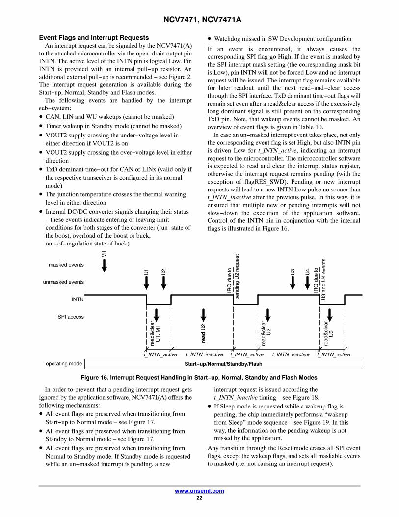
In case an un−masked interrupt event takes place, not onlythe corresponding event flag is set High, but also INTN pinis driven Low for t_INTN_active, indicating an interruptrequest to the microcontroller. The microcontroller softwareis expected to read and clear the interrupt status register,otherwise the interrupt request remains pending (with theexception of flagRES_SWD). Pending or new interruptrequests will lead to a new INTN Low pulse no sooner thant_INTN_inactive after the previous pulse. In this way, it isensured that multiple new or pending interrupts will notslow−down the execution of the application software.Control of the INTN pin in conjunction with the internalflags is illustrated in Figure 16.
Figure 16. Interrupt Request Handling in Start−up, Normal, Standby and Flash Modes
U1
U2
M1
read
&cl
ear
U1,
M1
read
U2
read
&cl
ear
U2
masked events
unmasked events
INTN
SPI access
U3
read
&cl
ear
U3
U4
t_INTN_active t_INTN_active t_INTN_activet_INTN_inactive t_INTN_inactive
IRQ
due
tope
ndin
g U
2 re
ques
t
IRQ
due
to
U3
and
U4
even
ts
operating mode Start−up/Normal/Standby/Flash
In order to prevent that a pending interrupt request getsignored by the application software, NCV7471(A) offers thefollowing mechanisms:• All event flags are preserved when transitioning from
Start−up to Normal mode – see Figure 17.• All event flags are preserved when transitioning from
Standby to Normal mode – see Figure 17.• All event flags are preserved when transitioning from
Normal to Standby mode. If Standby mode is requestedwhile an un−masked interrupt is pending, a new
interrupt request is issued according thet_INTN_inactive timing – see Figure 18.
• If Sleep mode is requested while a wakeup flag ispending, the chip immediately performs a “wakeupfrom Sleep” mode sequence – see Figure 19. In thisway, the information on the pending wakeup is notmissed by the application.
Any transition through the Reset mode erases all SPI eventflags, except the wakeup flags, and sets all maskable eventsto masked (i.e. not causing an interrupt request).

NCV7471, NCV7471A
www.onsemi.com23
Table 10. EVENT FLAGS SUMMARY
Event Flag BitRelated
Status Bit (Note 1)Related
Interrupt Mask Bit Set Condition Reset Condition
TxD
x Ti
me−
out flagTO_TxDC
none
intenTO_TxDCTxDx (Note 2) pin is kept Low forlonger than the time−out period
andcorresponding transceiver
in normal mode
read&clear access toregister STATUS0
and{TxDx (Note 2)
dominant time−outcondition disappeared
ortransceiver mode other
then “normal”}
flagTO_TxDL1 intenTO_TxDL1
flagTO_TxDL2 intenTO_TxDL2
SM
PS
flagBUCK_NOREG statBUCK_NOREG intenBUCK_NOREG
BUCK SMPS stage enters or leavesrange of no regulation (i.e. extreme
switching duty cycle); indicates(in)ability to reach nominal VOUT
read&clear access toregister STATUS0
flagBUCK_OL statBUCK_OL intenBUCK_OLBUCK SMPS stage enters or leaves
over−load condition (i.e. currentlimitation encountered or disappeared)
flagBOOST_RUN statBOOST_RUN intenBOOST_RUNBOOST SMPS stage changes activity– it starts or stops
flagBOOST_OL statBOOST_OL intenBOOST_OL
BOOST SMPS stage enters orleaves over−load condition (i.e.current limitation encountered or
disappeared)
flagTWAR statTWAR intenTWARjunction temperature crosses thewarning level in either direction
flagRES_SWD(Note 4) none intenRES_SWD
incorrect watchdog serviceencountered
anddevice in SW Development
configuration
VO
UT
2 flagVOUT2_UV statVOUT2_UV intenVOUT2_UV
VOUT2 under−voltage detectorchanges state in either direction
andVOUT2 is switched on
flagVOUT2_OV statVOUT2_OV intenVOUT2_OVVOUT2 over−voltage detector
changes state in either direction
flagSPIFail(Note 5) none intenSPIFail
SPI frame failure occurs:− number of SPI clocks differentfrom 0 or 16, or− SCK High when CSN changesstate
Wak
eups
flagWakeWU
none none
WU wakeup detected (Note 3)
Read&clear access toregister STATUS1
flagWakeCAN CAN wakeup detected (Note 3)
flagWakeLIN1 LIN1 wakeup detected (Note 3)
flagWakeLIN2 LIN2 wakeup detected (Note 3)
flagWakeTimer Timer wakeup detected (Note 3)
1. When a related status bit exists, the event is linked to a change (in either direction) of the status bit. Even if the event flag is cleared, thecorresponding status bit still indicates the current status of the observed feature and can be polled by SPI at any time.
2. “x” = “C”, “L1 or “L2”. In case of LIN transceivers, the time−out feature can be enabled/disabled by SPI.3. The respective wakeup source must be enabled through the corresponding control SPI register – timer wakeup in CONTROL0; CAN, LIN1/2
and WU wakeups in CONTROL14. For a missed WD in SW Development, INTN pulse is generated only once per event – it is not repeated even if the corresponding flag is
still set. New INTN pulse occurs only if WD is missed again in SW Development.5. During VOUT power−up (e.g. when going from Shut−down mode, or when waking−up from Sleep or Fail−safe mode), flagSPIFail can be
set because of transient toggling of internal CSN and SCK signals. It is therefore recommended to ignore flagSPIFail immediately after VOUTpower−up, until the STATUS0 register is reset. Except flagSPIFail, the remaining SPI register content is not influenced by the possible internaltoggling of CSN and SCK signals during power−up.

NCV7471, NCV7471A
www.onsemi.com24
Figure 17. Interrupt Request Handling during a Transition to Normal Mode
IRQ
due
to
pend
ing
U1
requ
est
U1
read
&cl
ear
U1
INTN
SPI access
t_INTN_inactivet_INTN_active t_INTN_active
Go
to N
orm
alor
Fla
sh
Start−up/Standby Normal/Flash
unmasked events
operating mode
Figure 18. Transition to Standby Mode with a Pending Interrupt Request
U1
read
&cl
ear
U1
INTN
SPI access
t_INTN_inactivet_INTN_active t_INTN_active
Go
toS
tand
by
IRQ
due
to
pend
ing
U1
requ
est
Normal Standby
unmasked events
operating mode
Figure 19. Attempted Transition to Sleep Mode with a Pending Wakeup Flag
U1
wakeup event
INTN
SPI access
Go
to
Normal Reset Start−up
RSTN
RS
TN
due
to
pend
ing
wak
eup
Inte
rrup
t fla
gs a
nd
mas
ks r
eset
in S
PI
read
&cl
ear
wak
eup
flag
Sleep(transient)
Sle
ep
After reset, WU and CAN/LIN wakeups disabled;pending flags will not cause additional INTN pulse
operatingmode

NCV7471, NCV7471A
www.onsemi.com25
Junction Temperature MonitoringThe device junction temperature is monitored in order to
avoid permanent degradation or damage of the chip. Twodistinct junction temperature thresholds are used:• Thermal warning level Tj_WAR. The status of the
current junction temperature compared with theTj_WAR threshold is available in the correspondingSPI status register. A change of the junctiontemperature across the warning threshold in eitherdirection sets the SPI bit flagTWAR. If not masked, aninterrupt request can be generated in order to signal tothe application that the junction temperature exceededor cooled below the warning level.
• Thermal shut−down level Tj_SD. Junction temperatureexceeding the shut−down level puts the chip intoFail−safe mode. In this specific case, no wakeups aredetected in the Fail−safe mode; the mode is auto−matically left only when the junction cools down belowthe warning level, thus providing a thermal margin forthe application software to cope with the event.
The junction temperature monitoring circuit is active in alloperating modes with VOUT supply switched on(Power−up, Reset, Start−up, Standby, Flash) and also in theFail−safe, provided that it has been entered as theconsequence of a thermal shut−down. The function of thejunction temperature monitoring of NCV7471(A) is shownin Figure 20.
Figure 20. Junction Temperature Monitoring
Power−up, Reset, Start−up, Normal, Stand−by, Flash
Tjunction belowwarning threshold
SPI TWAR status bit = 0
Tjunction abovewarning threshold
SPI TWAR bit = 1
Fail−safe mode
Tjunction aboveshutdown threshold
no wakeup detectionVOUT, VOUT2: offRSTN: Low
(if enabled)
flagTWAR −> 1;interrupt request
(if enabled)
Tj > Tj_WAR
Tj < Tj_WAR
Tj >
Tj_
SD
Tj < Tj_WAR
flagTWAR −> 1;interrupt request

NCV7471, NCV7471A
www.onsemi.com26
FSO1/2/3 – Fail−Safe OutputsNCV7471(A) offers three digital outputs dedicated to
control a fail−safe circuitry in the application under specificfailure conditions. All three outputs are high−voltagelow−side open drain drivers simultaneously activated by acommon internal signal FSO_internal and providingdifferent behavior:• FSO1 is constantly pulled Low if FSO_internal is active
• FSO2 provides 50% rectangular signal with 1.25 Hzfrequency
• FSO3 provides 20% rectangular signal with 100 Hzfrequency
Figure 21 illustrates the FSOx pins function with respect tothe internal FSO_internal signal.
Figure 21. Operation of FSOx Pins
FSO_internal is set to High as soon as a failure conditionis recognized or as soon as an SPI command is given toactivate FSO. Overview of situations leading toFSO_internal activation is given in Table 11. The handlingof the different failure conditions depends on the chipconfiguration (see the Configuration Mode section) –specifically in the SW development configuration, thewatchdog−related failures and “RSTN clamped Low”failure do not lead either to the FSO_internal activation orto the Fail−safe mode entry.
FSO_internal signal will be reset (and the FSOx outputsare subsequently de−activated) under the followingconditions:
• If FSO_internal was set by setting the FSO_ON SPI bit,it will be reset by writing “0” to FSO_ON SPI bit
• If FSO_internal was set because of a failure condition,a read−and−clear access to the flagFSO SPI status bitswill reset it.
In Start−up mode, FSO_internal High level limits SPIfunctionality – no register can be written or read&clearedwith the exception of CONTROL0 register. Attempts toperform a write or read&clear access to other registers willbe ignored – including attempts to reset bit FSO_ON or theflagFSO.x bits. This condition ensures that the applicationsoftware performs at least one successful watchdog serviceafter a failure occurs.

NCV7471, NCV7471A
www.onsemi.com27
Table 11. CONDITIONS FOR ACTIVATION OF FSO_INTERNAL SIGNAL (“X” Means “Don’t Care”)
FSO Activation Event Detected in Modes Detected in Configurations Fail−safe Mode Entered
Thermal Shutdown(Tj > Tjsd)
Power−upReset
Start−upNormalStandby
Flash
all yes
Fatal VOUT failure(VOUT < VOUT_FAIL for longer than
t_VOUT_powerup)
Power−up entered fromall the modes
all yes
VOUT undervoltage(VOUT < VOUT_RESx for longer thant_VOUT_powerup) (NCV7471A only)
Power−up entered fromConfiguration, Sleep or
Fail−safe
all no
VOUT undervoltage(VOUT < VOUT_RESx for longer than
t_VOUT_UV_filt) (NCV7471A only)
Power−up entered fromStart−up, Normal, Standby,
Flash
all no
RSTN Clamped High Reset all yes
External RSTN withoutprevious WD service
Start−up Config 1,2,3,4 no
RSTN Clamped Low when trying to leave Reset Config 1,3 no
Config 2,4 yes
1st Watchdog Missed Start−upNormalFlash
Standby (if WD on)
Config 1 no
Config 2 yes
2nd Watchdog Missed Start−upNormalFlash
Standby (if WD on)
Config 3 no
Config 4 yes
SPI control bit FSO set Start−upNormalStandby
Flash
all no
SWDM and CFG Digital InputsSWDM and CFG pins are high−voltage compliant digital
inputs enabling NCV7471(A) flexibility with respect to thefail−safe behavior. Their logical value (compared to alow−voltage digital threshold) is sensed and latchedexclusively in the Configuration operating mode – i.e. whenthe chip leaves the Shut−down mode. Subsequently, thelatched values are not changed by any signal on SWDM orCFG pin or by any SPI communication.
Latched active level on SWDM pin (i.e. High input levelin the Configuration mode) causes the chip to enter the SWdevelopment configuration regardless the state of CFG pin.When the latched SWDM value is inactive (i.e. Low in theConfiguration mode), the latched CFG value then controlswhether a failure condition (missed watchdog or RSTNclamped Low) results in the Fail−safe entry or only in a resetpulse generation. More details are given in the ConfigurationMode and FSO1/2/3 – Fail−Safe Outputs sections.

NCV7471, NCV7471A
www.onsemi.com28
SPI – Serial Peripheral Interface
SPI Frame FormatThe Serial Peripheral Interface ensures control of
NCV7471(A) operating modes, configuration of itsfunctions and read−out of internal status and systeminformation. The serial communication is achieved via SPIframes shown in Figure 22.
As long as the CSN chip select is High, the SCK and SDIinputs are not relevant and the SDO output is kepthigh−impedant. The signals on the SDI and SCK inputs aretaken into account only when CSN chip select input is set toLow. Data incoming on pin SDI are then sampled at thefalling edge of SCK clock signal; output data are shifted topin SDO at the rising edge of SCK clock signal. Bits aretransmitted MSB (most significant bit) first.
Figure 22. SPI Frame Format
A2 A1 A0 ReadOnly DI11 DI10 DI9 DI8 DI7 DI6 DI5 DI4 DI3 DI2 DI1 DI0
DO11 DO10 DO9 DO8 DO7 DO6 DO5 DO4 DO3 DO2 DO1 DO0HZ HZ
header data
X X
CSN
SCK
SDI
A2 A1 A0 ReadOnly
SPIreadySDO
One frame consists of exactly sixteen bits transferred fromthe microcontroller to NCV7471(A) through input pin SDI.The input bits are interpreted as follows:• Immediately after CSN falling edge, SDO pin shows an
internal “SPI ready” flag. Under normal conditions,when the inter−frame space is respected, the “SPIready” flag is set to High and the device is available forSPI communication. If the SPI inter−frame space isviolated, the previous SPI data might not be processedat the moment of the next CSN Low level; this situationis signaled by Low “SPI ready” flag. If the applicationsoftware still attempts to perform SPI communication,incoming data will be completely ignored and the SDOsignals “Low” throughout the SPI frame. The status ofthe flag is latched at the CSN falling edge – theapplication software might use short Low pulses onCSN (without SCK) in order to poll the flag.
• Four most significant bits form the header of the SPIframe. During the reception of the header bits, the SDIsignal is looped back to the SDO pin starting with thefirst rising edge of SCK – except for the internal delay,signals SDO and SDI are equal during the headertransmission. The header bits have the followingfunction:♦ Bits A2, A1, and A0 form a 3−bit address of an
internal SPI register. NCV7471(A) contains eighttwelve−bit registers addressable by these threeheader bits.
♦ Bit “ReadOnly” contains the “read−only” flag. IfReadOnly=High, the current SPI frame represents aread−only access to the SPI register. IfReadOnly=Low, then the current SPI framerepresents either a write or read−and−clear access toan SPI register – the distinction between “write” and“read−and−clear” access depends on the specificregister.
• Bits DI11−DI0 are the SPI data. In case of a read−onlyor read−and−clear access, these bits are ignored. In caseof a write−frame, these bits are taken as the new SPIregister content at the moment of the CSN rising edge(when the frame is considered finished). Regardless theaccess type, the output data DO11−DO0 represent theSPI register content as valid at the beginning of the SPIframe. The output bits are shifted−out at the rising edgeof the SCK clock so that they can be sampled by themicrocontroller at the SCK falling edge.The following checks are performed on every SPI frame:
• The SCK clock input must be Low at both edges of theCSN chip select signal
• There must be exactly sixteen SCK clock cycles whenCSN=Low (or no SCK edge if only the “SPI ready”flag is polled).
If any of the above conditions is not fulfilled, the SPI frameis considered incorrect and the “SPI Fail” event is internallygenerated.

NCV7471, NCV7471A
www.onsemi.com29
SPI Register Mapping
Table 12. SPI REGISTERS MAPPING
AddressRegister Name
Register Content
A2 A1 A0 D11 D10 D9 D8 D7 D6 D5 D4 D3 D2 D1 D0
0 0 0 CONTROL0
OP
MO
DE
.2
OP
MO
DE
.1
OP
MO
DE
.0
WD
_MO
D.1
WD
_MO
D.0
WD
_PE
R.2
WD
_PE
R.1
WD
_PE
R.0
CH
EC
KS
UM
rese
rved
rese
rved
rese
rved
inpu
t
RE
S_S
RC
.3
RE
S_S
RC
.2
RE
S_S
RC
.1
RE
S_S
RC
.0
outp
ut
0 0 1 CONTROL1re
serv
ed
enV
OU
T2
mod
WU
.1
mod
WU
.0
mod
CA
N.1
mod
CA
N.0
enLI
N_L
SLP
disT
O_T
xDL
mod
LIN
2.1
mod
LIN
2.0
mod
LIN
1.1
mod
LIN
1.0
0 1 0 CONTROL2
rese
rved
rese
rved
rese
rved
rese
rved
rese
rved
FS
O_O
N
FAS
T_F
SO
VO
UT
_RE
S.1
VO
UT
_RE
S.0
mod
DC
DC
.1
mod
DC
DC
.0
enB
OO
ST
0 1 1 CONTROL3
inte
nTO
_TxD
C
inte
nTO
_TxD
L1
inte
nTO
_TxD
L2
inte
nBU
CK
_NO
RE
G
inte
nBU
CK
_OL
inte
nBO
OS
T_R
UN
inte
nBO
OS
T_O
L
inte
nTW
AR
inte
nRE
S_S
WD
inte
nVO
UT
2_U
V
inte
nVO
UT
2_O
V
inte
nSP
IFai
l
1 0 0 STATUS0
flagT
O_T
xDC
flagT
O_T
xDL1
flagT
O_T
xDL2
flagB
UC
K_N
OR
EG
flagB
UC
K_O
L
flagB
OO
ST
_RU
N
flagB
OO
ST
_OL
flagT
WA
R
flagR
ES
_SW
D
flagV
OU
T2_
UV
flagV
OU
T2_
OV
flagS
PIF
ail
1 0 1 STATUS1
rese
rved
rese
rved
rese
rved
flagF
SO
.3
flagF
SO
.2
flagF
SO
.1
flagF
SO
.0
flagW
akeW
U
flagW
akeC
AN
flagW
akeL
IN1
flagW
akeL
IN2
flagW
akeT
imer
1 1 0 STATUS2
rese
rved
stat
VS
_LO
W
stat
BU
CK
_NO
RE
G
stat
BU
CK
_OL
stat
BO
OS
T_R
UN
stat
BO
OS
T_O
L
stat
SW
DM
stat
CF
G
stat
WU
stat
TW
AR
stat
VO
UT
2_U
V
stat
VO
UT
2_O
V
1 1 1 GENERAL PURPOSE
GP
D.1
1
GP
D.1
0
GP
D.9
GP
D.8
GP
D.7
GP
D.6
GP
D.5
GP
D.4
GP
D.3
GP
D.2
GP
D.1
GP
D.0
NOTE: “reserved” bits in input data are ignored; they are set to Low in output data.

NCV7471, NCV7471A
www.onsemi.com30
Table 13. SPI REGISTERS INITIALIZATION
AddressRegister
Name
Initialization ReadOnly bit
A2 A1 A0 Initialized in (Note 6) Initial content Low (Note 7) High
0 0 0 CONTROL0 Reset mode(except Flashmode entry)
Watchdog set totime−out @
256 ms nominal
Mode and Watchdogsettings (bits DI11−DI4)written into the register ifchecksum (bit DI3) is OK.Input bits DI2−DI0 ignored.
Input dataignored;currentregister
content sentto SPI output
0 0 1 CONTROL1 Power−up mode all bits Low(Note 9)
Bits DI11−DI0 written intothe register
Reset mode all bits Low(Note 9)
0 1 0 CONTROL2 Configuration all bits Low Bits DI11−DI0 written intothe register
Sleep all bits Low
0 1 1 CONTROL3 Reset mode all bits Low Bits DI11−DI0 written intothe register
1 0 0 STATUS0 Reset mode all bits Low read&clear access;all bits reset to Low (Note 8);
input data ignored
1 0 1 STATUS1 Configuration mode all bits Low read&clear access;all bits reset to Low; input
data ignored
1 1 0 STATUS2 n.a. Reflects status ofinternal blocks
input data ignored
1 1 1 GENERALPURPOSE
Configurationmode
register filled withdevice ID data
Bits DI11−DI0 written intothe register
6. In modes not explicitly listed in “Initialized in” column, the register content is preserved7. Regardless the access type (the “ReadOnly” bit), the current register content is always sent to the SPI output8. Bits containing TxD dominant timeout flags will remain set if the excessively long dominant signal persists on the respective TxDx pin9. Exception: in SW Development configuration, CONTROL1 bits modCAN.x, modLIN1.x and modLIN2.x are all set to “High”, corresponding
to the default “Normal” mode of all transceivers

NCV7471, NCV7471A
www.onsemi.com31
CONTROL0 Register (Address 000)By a write access to the CONTROL0 register
(“ReadOnly” = Low), the application software can controlthe operating mode of NCV7471(A) and the watchdogsettings. A write access represents a watchdog service. Anoperating mode change is therefore always synchronizedwith the watchdog trigger message. In order to provide moresafety to the mode control, the input data are protected witha check−sum (input bit DI3). The checksum mustcorrespond to the following formula (symbol “⊕” denotingthe exclusive−or operation):
In case of incorrect checksum in written data, the devicereacts identically to a wrong opmode situation. During aread−only access to the CONTROL0 register (“ReadOnly”= High), the input data are completely ignored and no checkis performed on them.
The output data of the CONTROL0 register – regardlessthe access type − indicate the current operating mode, thecurrent watchdog settings and the cause of the last reset.
The initialization of the CONTROL0 register content isperformed after every reset, when the watchdog type is fixedto time−out, and the watchdog period to nominally 256 ms.
DI3 = DI11 ⊕ DI10 ⊕ DI9 ⊕ DI8 ⊕ DI7 ⊕ DI6 ⊕ DI5 ⊕ DI4
Table 14. CONTROL0 REGISTER: OPMODE.x Encoding
OP
MO
DE
.2
OP
MO
DE
.1
OP
MO
DE
.0
OPMODE.x in Input Data
OPMODE.xin Output
Data
RequestedMode
Reactionin Start−up
Reactionin Normal
Reactionin Standby
Reactionin Flash
CurrentMode
0 0 0 forbidden “Wrong Opmode” Reset Start−up
0 0 1 Normal go to Normal keep Normal go to Normal return fromFlash viaReset andStart−up
Normal
0 1 0 Standby “Wrong Opmode”Reset
go to Standby keep Standby “WrongOpmode”
Reset
Standby
0 1 1 Sleep “Wrong Opmode”Reset
go to Sleep “Wrong Opmode” Reset not used
1 0 0 Flash go to Flash viaReset
go to Flash viaReset
“WrongOpmode” Reset
keep Flash Flash
1 0 1 Fail−safe in SW development configuration, go to Fail−safe;otherwise “Wrong Opmode” Reset
not used
1 1 0 Reset go to Reset not used
1 1 1 Configuration go toConfiguration
go to Configuration “Wrong Opmode” Reset not used
Table 15. CONTROL0 REGISTER: WD_MOD.x Encoding
WD
_MO
D.1
WD
_MO
D.0
Watchdog Timer ModeLimitations
(if not respected, the write access is considered as a missed watchdog)
0 0 Watchdog off Can be used only with a Standby or a Sleep mode request
0 1 Window Watchdog Can be used only for Normal mode request
1 0Time−out Watchdog Must be used with every Flash mode request;
can be used with a Standby or Normal mode request;default in Start−up mode
1 1 Timer Wakeup Can be used only with a Standby mode request

NCV7471, NCV7471A
www.onsemi.com32
Table 16. CONTROL0 REGISTER: WD_PER.x EncodingW
D_P
ER
.2
WD
_PE
R.1
WD
_PE
R.0
Watchdog Peri-od Nominal Duration Note
0 0 0 WD_PER_0 8 ms
0 0 1 WD_PER_1 16 ms
0 1 0 WD_PER_2 32 ms
0 1 1 WD_PER_3 64 ms
1 0 0 WD_PER_4 128 ms
1 0 1 WD_PER_5 256 ms WD_PER_5 is automatically used in Start−up mode
1 1 0 WD_PER_6 512 ms Can be used only for Standby and Flash modes (otherwise the watchdog SPI frame is considered wrong)
1 1 1 WD_PER_7 1024 ms
Table 17. CONTROL0 REGISTER: RES_SRC.x Encoding
RE
S_S
RC
.3
RE
S_S
RC
.2
RE
S_S
RC
.1
RE
S_S
RC
.0
Cause of the Last RSTN Pulse
Reset EventPriority
(Note 10)
0 0 0 0 V_MID under−voltage recovery (V_IN connection) 12
0 0 0 1 External reset outside Start−up mode (not accompanied by FSO activation) 10
0 0 1 0 Recovery from Fail−safe (through wakeup or thermal shutdown recovery) 8
0 0 1 1 Wakeup from Sleep 7
0 1 0 0 Flash mode requested 6
0 1 0 1 Flash mode exited 5
0 1 1 0 Reset mode requested 4
0 1 1 1 Configuration requested 3
1 0 0 0 Failed Watchdog (WD missed, wrong WD mode or period requested) − will not be used inSW Development configuration (Note 11)
2
1 0 0 1 Wrong operating mode requested; wrong checksum during write access to the Mode Con-trol register
1
1 0 1 0 External reset in Start−up mode (accompanied by FSO activation if not in SW Develop-ment configuration)
9
1 0 1 1 reserved −
1 1 0 0 reserved −
1 1 0 1 reserved −
1 1 1 0 reserved −
1 1 1 1 VOUT under−voltage recovery 11
10.The “Reset Event Priority” reflects the order, in which the reset events are processed by the on−chip digital. In case more events occursimultaneously, the one with the lower priority number would be stored in CONTROL0 register.
11. WD period and WD mode settings are not checked in the following situations: Configuration mode request, Reset mode request, Flash exit(i.e. Normal mode request in the course of Flash mode)

NCV7471, NCV7471A
www.onsemi.com33
CONTROL1 Register (Address 001)CONTROL1 register defines the mode of individual CAN and LINx transceivers, of the VOUT2 regulator and the WU pin.
The encoding of the CONTROL1 bits is defined in Table 18.
Table 18. CONTROL1 REGISTER ENCODING
enVOUT2 VOUT2 control
0 VOUT2 regulator is OFF
1 VOUT2 regulator is ON
modWU.1 modWU.0 WU mode control
0 0 WU wakeup detection disabled
0 1 WU monitored for falling edge
1 0 WU monitored for rising edge
1 1 WU monitored for both edges
modCAN.1 modCAN.0 CAN transceiver mode
0 0 CAN transceiver in Off mode
0 1 CAN transceiver in Wakeup mode
1 0 CAN transceiver in Receive−only mode
1 1 CAN transceiver in Normal mode
enLIN_LSLP LIN slope control – common for both LIN channels
0 LIN transmission with normal bus signal slopes (according LIN2.1 specification)
1 LIN transmission with slow bus signal slopes (for limited bit−rate)
disTO_TxDL LIN dominant time−out control – common for both LIN channels
0 Dominant time−out applied on TxDL pins
1 Dominant time−out not−applied on TxDL pins – unlimited dominant symbols can be transmitted
modLINx.1 modLINx.0 LINx transceiver mode (x=1,2)
0 0 LINx transceiver in Off mode
0 1 LINx transceiver in Wakeup mode
1 0 LINx transceiver in Receive−only mode
1 1 LINx transceiver in Normal mode
CONTROL1 register is initialized at every reset event with all−zeros content

NCV7471, NCV7471A
www.onsemi.com34
CONTROL2 Register (Address 010)Content of CONTROL2 register is defined in Table 19. The CONTROL2 register content is initialized to all−zeros content
in the Configuration and Sleep modes.
Table 19. CONTROL2 REGISTER ENCODING
Bit Definition
FSO_ON If High, FSOx outputs are forced active
FAST_FSO If High, already the 1st missed watchdog will be treated as a failure;the exact reaction depends on the configuration
VOUT_RES.1 VOUT_RES.0 Selection of VOUT under−voltage threshold for RSTN Pin
0 0 VOUT_RES4 threshold selected (the lowest threshold) for RSTN indication
0 1 VOUT_RES3 threshold selected for RSTN indication
1 0 VOUT_RES2 threshold selected for RSTN indication
1 1 VOUT_RES1 threshold selected for RSTN indication
modDCDC.1 modDCDC.0 DCDC Converter mode selection
0 0 DCDC Converter switching with fixed frequency
0 1 Converter switching frequency modulated with modulation depth dmod_DCDC_1
1 0 Converter switching frequency modulated with modulation depth dmod_DCDC_2
1 1 Converter switching frequency modulated with modulation depth dmod_DCDC_3
enBOOST If High, BOOST (step−up) stage of the DCDC converter is enabled
CONTROL3 Register (Address 011)The individual bits in the CONTROL3 register determine
whether the corresponding interrupt event leads to aninterrupt request via INTN pin or if it is only stored as a flagfor later SPI retrieval. If the bit is High, the interrupt request
is enabled. All bits of the CONTROL3 register are reset toLow at every reset event (i.e. all interrupt sources aredisabled).
Table 20. CONTROL3 REGISTER ENCODING
Bit Definition
intenTO_TxDC Enables interrupt after dominant time−out on TxDC
intenTO_TxDL1 Enables interrupt after dominant time−out on TxDL1
intenTO_TxDL2 Enables interrupt after dominant time−out on TxDL2
intenBUCK_NOREG Enables interrupt after a change of the internal converter signal indicating, that the buck stage cannot reach theoutput nominal voltage (typically due to too low line voltage)
intenBUCK_OL Enables interrupt after a change of the internal converter signal indicating, that the buck stage is overloaded
intenBOOST_RUN Enables interrupt when the boost stage is activated or de−activated – indicating a change in supply line conditions
intenBOOST_OL Enables interrupt after a change of the internal converter signal indicating, that the boost stage is overloaded
intenTWAR Enables interrupt when the junction temperature crosses the thermal warning level (in either direction)
intenRES_SWD In SW Development configuration only – incorrect watchdog service will lead to an interrupt request(outside SW Development configuration, this event would lead to reset).
intenVOUT2_UV Enables interrupt when VOUT2 crosses its under−voltage level (in either direction).Event registered only if VOUT2 is on.
intenVOUT2_OV Enables interrupt when VOUT2 crosses its over−voltage level (in either direction).
intenSPIFail Enables interrupt when an SPI frame failure is encountered

NCV7471, NCV7471A
www.onsemi.com35
STATUS0 Register (Address 100)STATUS0 bits latch information on individual events
which can potentially lead to interrupt requests. All bits havetheir position corresponding to the CONTROL3 registerbits. The details of the STATUS0 bits are given in Table 21.
A read−and−clear access to STATUS0 register isconsidered “interrupt service” for all pending interruptrequests. A read−only access does not change the flags andthe active interrupt requests remain pending.
Specifically, flags corresponding to dominant time−outscan be cleared only when the respective time−outdisappeared; otherwise, they will remain set even afterread&clear access and, if enabled, the interrupt linked tothem will remain pending.
STATUS0 register is reset to all−zeros content at everyreset event.
Table 21. STATUS0 REGISTER ENCODING
Bit Definition
flagTO_TxDC TxDC dominant time−out occurred. The bit can be cleared only when the time−out condition disappeared(or when the CAN transceiver mode was changed to other than “CAN Normal”).
flagTO_TxDL1 TxDL1 dominant time−out occurred. The bit can be cleared only when the time−out condition disappeared (orwhen the LIN1 transceiver mode was changed to other than “LIN Normal”).
flagTO_TxDL2 TxDL2 dominant time−out occurred. The bit can be cleared only when the time−out condition disappeared (orwhen the LIN2 transceiver mode was changed to other than “LIN Normal”).
flagBUCK_NOREG Flags a change of the internal converter signal indicating, that the buck stage cannot reach the output nominalvoltage (typically due to too low line voltage)
flagBUCK_OL Flags a change of the internal converter signal indicating, that the buck stage is overloaded
flagBOOST_RUN Boost stage toggled its state (was activated or de−activated) – indicating a change in supply line conditions
flagBOOST_OL Flags a change of the internal converter signal indicating, that the boost stage is overloaded
flagTWAR Junction temperature crossed the thermal warning level (in either direction)
flagRES_SWD In SW Development configuration only – incorrect watchdog service occurred
flagVOUT2_UV VOUT2 crossed its under−voltage level (in either direction). Event registered only if VOUT2 is on.
flagVOUT2_OV VOUT2 crossed its over−voltage level (in either direction).
flagSPIFail SPI frame failure was encountered (Note 12)
12.During VOUT power−up (e.g. when going from Shut−down mode, or when waking−up from Sleep or Fail−safe mode), flagSPIFail can beset because of transient toggling of internal CSN and SCK signals. It is therefore recommended to ignore flagSPIFail immediately after VOUTpower−up, until the STATUS0 register is reset. Except flagSPIFail, the remaining SPI register content is not influenced by the possible internaltoggling of CSN and SCK signals during power−up.

NCV7471, NCV7471A
www.onsemi.com36
STATUS1 Register (Address 101)STATUS1 register contains flags for fail−safe events and
wakeups. A specific bit (flag) is set High when thecorresponding event was recognized and is set to Low onlywhen the STATUS1 register is read and cleared. The
STATUS1 register is initialized in Configuration mode toall−zeros content. It is not reset in Reset or Start−up mode inorder to preserve the wakeup and failure flags coming fromSleep or Fail−safe mode. Encoding of the FSO−related flagbits is defined in Table 22.
Table 22. STATUS1 REGISTER: flagFSO.x Encoding
flagFSO.3 flagFSO.2 flagFSO.1 flagFSO.0 Failure event leading to FSOx activation
0 0 0 0 no failure, FSOx inactive (unless over−ruled by FSO_ON bit)
0 0 0 1 FSOx active due to missed watchdog; without entry into Fail−safe mode
0 0 1 0 FSOx active due to “RSTN clamped Low”; without entry into Fail−safe mode
0 0 1 1 FSOx active due to external reset in Start−up mode; without entry into Fail−safe mode (not detected in SW Development configuration)
0 1 0 0 reserved
0 1 0 1 reserved
0 1 1 0 reserved
0 1 1 1 reserved
1 0 0 0 FSOx active; coming from Fail−safe mode requested by SPI
1 0 0 1 FSOx active; coming from Fail−safe mode caused by missed watchdog
1 0 1 0 FSOx active; coming from Fail−safe mode caused by “RSTN clamped Low”
1 0 1 1 FSOx active; coming from Fail−safe mode caused by “RSTN clamped High”
1 1 0 0 FSOx active; coming from Fail−safe mode caused by thermal shutdown
1 1 0 1 FSOx active; coming from Fail−safe mode caused by VOUT undervoltagetime−out (short−circuit detected) or FSOx active due to VOUT undervoltage(NCV7471A only)
1 1 1 0 reserved
1 1 1 1 reserved
Wakeup flag bits are summarized in Table 23. Detectionof individual wakeup events is controlled by transceivermode settings (for LIN and CAN wakeup), WU pin modesettings (for WU wakeup) and watchdog settings (for timerwakeup). A wakeup event is indicated either by an interrupt
request (in Normal or Standby mode) or by a reset pulse(wakeups from Sleep mode). In Normal and Standby mode,a wakeup causes pending interrupt request until aread−and−clear access to STATUS1 register.
Table 23. STATUS1 REGISTER: Wakeup Flags
Bit Definition
flagWakeWU Wakeup on WU pin was detected (for non−zero setting of modWU.x SPI bits)
flagWakeCAN Wakeup on CAN bus was detected (CAN transceiver in “CAN Wakeup” mode)
flagWakeLIN1 Wakeup on LIN1 bus was detected (LIN1 transceiver in “LIN Wakeup” mode)
flagWakeLIN2 Wakeup on LIN2 bus was detected (LIN2 transceiver in “LIN Wakeup” mode)
flagWakeTimer Wakeup by timer (“Timer wakeup” selected through CONTROL0 register)

NCV7471, NCV7471A
www.onsemi.com37
STATUS2 Register (Address 110)STATUS2 register bits reflect the state of several internal blocks of the device. Read−and−clear or write access does not
change the register content. The STATUS2 bits are defined in Table 24.
Table 24. STATUS2 REGISTER ENCODING
Bit Definition
statVS_LOW Indication of the VS monitoring output. If VS<VS_MON, then statVS_LOW = 1
statBUCK_NOREG Indication of the buck DCDC stage not being able to reach the nominal VOUT voltage
statBUCK_OL Indication of the buck DCDC stage overload
statBOOST_RUN Indication that the boost DCDC stage is running(boost stage must be enabled and the input voltage requires step−up operation)
statBOOST_OL Indication of the boost DCDC stage overload
statSWDM Logical level of the SWDM pin latched during Configuration mode
statCFG Logical level on the CFG pin latched during Configuration mode (in Config 1,2,3,4)orCurrent logical level on CFG pin (in SW Development)
statWU Logical level on the WU pin
statTWAR Output of the thermal warning comparator (if High, junction temperature is above the warning level)
statVOUT2_UV Output of the VOUT2 under−voltage comparator (if High, VOUT2 is below the under−voltage level).Available only if VOUT2 regulator is on.
statVOUT2_OV Output of the VOUT2 over−voltage comparator (if High, VOUT2 is above the over−voltage level)
GENERAL PURPOSE Register (Address 111)General Purpose register allows storing general 12−bit
information in the NCV7471(A) memory. The register isinitialized only in Configuration mode, when a deviceversion ID is loaded. Any data written to the registeroverwrite the initial content and are kept throughout the
operation of the device until device enters Shut−down modeor until Configuration is requested.
The device ID is:• 0x103 or 0x143 for NCV7471,
• 0x144 or 0x184 for NCV7471A.

NCV7471, NCV7471A
www.onsemi.com38
Table 25. ABSOLUTE MAXIMUM RATINGS
Symbol Parameter Min Max Units
Vmax_VS Maximum voltage at VS pin −0.3 40 V
Vmax_VS_VOUT2 Maximum voltage at VS_VOUT2 pin −0.3 40 V
Vmax_BOOST Maximum voltage at BOOST pin −0.3 V_MID+2 V
Vmax_V_MID Maximum voltage at V_MID pin −0.3 40 V
Vmax_BUCK Maximum DC voltage at BUCK pinMaximum transient voltage on BUCK pin (Note 13)
−1−3
V_MID+0.3 V
Vmax_VOUT Maximum voltage at VOUT pin −0.3 6 V
Vmax_VOUT2 Maximum voltage at VOUT2 pin −1 40 V
Vmax_VCC_CAN Maximum voltage at VCC_CAN pin −0.3 6 V
Vmax_CANH,Vmax_CANL
Maximum voltage at CAN bus pins(0 < VCC_CAN < 5.25 V; no time limit)
−50 50 V
Vmax_LINx Maximum voltage at LIN bus pins −45 45 V
Vmax_FSOx Maximum voltage at FSOx pins −0.3 40 V
Vmax_WU Maximum voltage at WU pin −40 40 V
Vmax_CFG; Vmax_SWDM Maximum voltage at CFG and SWDM pins −0.3 40 V
Vmax_digIn Maximum voltage at digital input and open−drain pins(TxDLx, TxDC, SCK, SDI, INTN, RSTN, UVN_VOUT)
−0.3 6 V
Vmax_digOut Maximum voltage at digital push−pull output pins(RxDLx, RxDC, SDO)
−0.3 VOUT+0.3 V
Vmax_CSN Maximum voltage at CSN pin −0.3 40 V
Tjunc_max Junction temperature −40 +170 °C
V_ESD System ESD on pins CANH, CANL, LIN1, LIN2, VOUT2, VS,VS_VOUT2, WU as per IEC 61000−4−2: 330 � / 150 pF
≥ ±6 kV
Human body model on pins CANH, CANL, LIN1, LIN2stressed towards GND with 1500 � / 100 pF
≥ ±6 kV
Human body model on pins VS, VS_VOUT2, WUstressed towards GND with 1500 � / 100 pF
≥ ±4 kV
Human body model on all pinsas per JESD22−A114 / AEC−Q100−002
≥ ±2 kV
Charge device model on all pinsas per JESD22−C101 / AEC−Q100−011
≥ ±500 V
MSL Moisture Sensitivity Level 2
Stresses exceeding those listed in the Maximum Ratings table may damage the device. If any of these limits are exceeded, device functionalityshould not be assumed, damage may occur and reliability may be affected.13.BUCK pin tolerates transient voltage excursions below −1 V, caused by the buck−converter switching and the non−ideal characteristics of
diode D2 (see Figure 2). It is not implied that a hard voltage source of less than −1 V can be connected to the pin externally.
Table 26. THERMAL CHARACTERISTICS
Symbol Parameter Value Units
R�JC Thermal resistance junction−to−case 3.9 °C/W

NCV7471, NCV7471A
www.onsemi.com39
Table 27. OPERATING RANGES
Symbol Parameter Min Max Units
Vop_V_IN_boostbuck V_IN operating voltage for boost/buck operation 2.5 28 V
Vop_V_IN_buck V_IN operating voltage for buck−only operation 6 28 V
Vop_VS Operating voltage at VS pin 6 28 V
Vop_VS_VOUT2 Operating DC voltage at VS_VOUT2 pin 6 28 V
Vop_BOOST Operating voltage at BOOST pin 0 V_MID+V_D1 V
Vop_V_MID Operating voltage at V_MID pin 5.5 28 V
Vop_BUCK Operating voltage at BUCK pin −V_D2 V_MID V
Vop_VOUT Regulated voltage at VOUT2 supply output 4.9 5.1 V
Vop_VOUT2 Regulated voltage at VOUT2 supply output 4.9 5.1 V
Vop_VCC_CAN_normal Operating voltage at VCC_CAN pin for normal andreceive only CAN modes
4.75 5.25 V
Vop_VCC_CAN_lowpower Operating voltage at VCC_CAN pin for wakeup and offCAN modes
0 5.25 V
Vop_CANH,Vop_CANL
Operating voltage at CAN bus pins 0 VCC_CAN V
Vop_LINx Operating voltage at LIN bus pins 0 VS V
Vop_FSOx Operating voltage at FSOx pins 0 VS V
Vop_WU Operating voltage at WU pin 0 VS V
Vop_CFG; Vop_SWDM
Operating voltage at CFG and SWDM pins 0 VS V
Vop_digIO Operating voltage at digital input and output pins(TxDLx, RxDLx, TxDC, RxDC, SCK, CSN, SDI, SDO,INTN, RSTN, UVN_VOUT)
0 VOUT V
Tjunc_op Junction temperature −40 +150 °C
Functional operation above the stresses listed in the Recommended Operating Ranges is not implied. Extended exposure to stresses beyondthe Recommended Operating Ranges limits may affect device reliability.
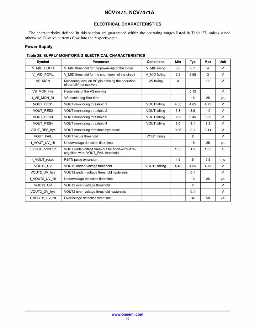
NCV7471, NCV7471A
www.onsemi.com40
ELECTRICAL CHARACTERISTICS
The characteristics defined in this section are guaranteed within the operating ranges listed in Table 27, unless statedotherwise. Positive currents flow into the respective pin.
Power Supply
Table 28. SUPPLY MONITORING ELECTRICAL CHARACTERISTICS
Symbol Parameter Conditions Min Typ Max Unit
V_MID_PORH V_MID threshold for the power−up of the circuit V_MID rising 3.3 3.7 4 V
V_MID_PORL V_MID threshold for the shut−down of the circuit V_MID falling 2.2 2.65 3 V
VS_MON Monitoring level on VS pin defining the operationof the LIN transceivers
VS falling 3 5.2 V
VS_MON_hys Hysteresis of the VS monitor 0.12 V
t_VS_MON_filt VS monitoring filter time 16 25 �s
VOUT_RES1 VOUT monitoring threshold 1 VOUT falling 4.55 4.65 4.75 V
VOUT_RES2 VOUT monitoring threshold 2 VOUT falling 3.8 3.9 4.0 V
VOUT_RES3 VOUT monitoring threshold 3 VOUT falling 3.35 3.45 3.55 V
VOUT_RES4 VOUT monitoring threshold 4 VOUT falling 3.0 3.1 3.2 V
VOUT_RES_hys VOUT monitoring threshold hysteresis 0.03 0.1 0.14 V
VOUT_FAIL VOUT failure threshold VOUT rising 2 V
t_VOUT_UV_filt Undervoltage detection filter time 16 25 �s
t_VOUT_powerup VOUT undervoltage time−out for short−circuit re-cognition w.r.t. VOUT_FAIL threshold
1.35 1.5 1.65 s
t_VOUT_reset RSTN pulse extension 4.5 5 5.5 ms
VOUT2_UV VOUT2 under−voltage threshold VOUT2 falling 4.45 4.65 4.75 V
VOUT2_UV_hys VOUT2 under−voltage threshold hysteresis 0.1 V
t_VOUT2_UV_filt Undervoltage detection filter time 16 25 �s
VOUT2_OV VOUT2 over−voltage threshold 7 V
VOUT2_OV_hys VOUT2 over−voltage threshold hysteresis 0.1 V
t_VOUT2_OV_filt Overvoltage detection filter time 32 50 �s

NCV7471, NCV7471A
www.onsemi.com41
Table 29. DC/DC CONVERTER ELECTRICAL CHARACTERISTICS
Symbol Parameter Conditions Min Typ Max Unit
VOUT DCDC output voltage NCV7471(A) in Normal or Standby;Suitable external components for
the required load current and inputvoltage used.
4.9 5.0 5.1 V
I_OUT DCDC output current available for ex-ternal loads (see Figure 2)
NCV7471(A) in Normal or Standby;function of external components
500 mA
Imaxpeak_BOOST Maximum peak−current detectionthreshold in BOOST stage
Tj ≤ 0°CTj > 0°C
1.61.6
2.22.0
A
Imaxpeak_BUCK Maximum peak−current detectionthreshold in BUCK stage
0.8 1.0 A
V_MID_reg Middle voltage level Boosting active 6.175 6.5 6.825 V
Ron_BOOST On−resistance of the boost−stageswitch
0.45 �
Ron_BUCK On−resistance of the buck−stage switch 0.6 �
V_MID_Ron V_MID level for parametrical on−resist-ance of the converter switches
5 V
fsw_DCDC Constant switching frequency 450 485 520 kHz
fmod_DCDC Modulation frequency Modulation enabled via SPI 8 10 13 kHz
dmod_DCDC_1 Modulation depth 1 10 %
dmod_DCDC_2 Modulation depth 2 20 %
dmod_DCDC_3 Modulation depth 3 30 %
Product parametric performance is indicated in the Electrical Characteristics for the listed test conditions, unless otherwise noted. Productperformance may not be indicated by the Electrical Characteristics if operated under different conditions.
Table 30. VOUT2 REGULATOR ELECTRICAL CHARACTERISTICS
Symbol Parameter Conditions Min Typ Max Unit
VOUT2 VOUT2 regulator output voltage VOUT2 regulator active;Iload(VOUT2) ≤ 5 mA
4.95 5.0 5.05 V
VOUT2 regulator active;Iload(VOUT2) ≤ 50 mA
4.9 5.0 5.1 V
VOUT2_drop Drop−out voltage between VS_VOUT2and VOUT2
Iload(VOUT2) = 50 mA 0.35 0.6 V
Ilim_VOUT2 VOUT2 current limitation VOUT2 regulator active −80 mA

NCV7471, NCV7471A
www.onsemi.com42
Table 31. CURRENT CONSUMPTIONS
Symbol Parameter Conditions Min Typ Max Unit
I_VS(Note 14)
VS consumption in LIN nor-mal mode
LIN1 and LIN2 in Normal mode;recessive on both LIN buses
3.2 mA
VS consumption with LIN inWakeup or Off mode
LIN1 and LIN2 in LIN−wakeup or Off mode;no activity on both LIN buses; Tj ≤ 85°C
8 �A
I_VS_VOUT2(Note 14)
VS_VOUT2 consumption ifVOUT2 is on
VOUT2 regulator is active 30 �A+
1.1 xI(VOUT2)
−
VS_VOUT2 consumption ifVOUT2 is off
VOUT2 regulator is off;VS_VOUT2 ≤ 13.5 V; Tj ≤ 85°C
1 �A
I_VCC_CAN(Note 14)
VCC_CAN consumption fordominant transmission
CAN in Normal mode driving dominant onthe CAN bus; 60 � load on the CAN pins
75 mA
VCC_CAN consumption forrecessive transmission
CAN in Receive−only mode or CAN inNormal mode with recessive on the bus
10 mA
VCC_CAN consumption inCAN Wakeup mode
CAN Wakeup mode (CAN supplied from V_MID);
Device in Standby or Sleep mode;no wakeup detected; Tj ≤ 85°C
2 �A
I_IN(Notes 14, 16)
DCDC input current inStandby or Normal mode
NCV7471(A) in Standby or Normal mode;V_IN (Note 15) = 13.5 V; Tj ≤ 85°C;
no external VOUT loadenBoost = Low;
CAN in Off mode
70 95 �A
DCDC input current inSleep mode
NCV7471(A) in Sleep mode;5.5 V ≤ V_IN (Note 15) ≤ 18 V; Tj ≤ 85°C;
enBoost = Low;CAN in Off mode
55 70 �A
I_IN adder for CAN wakeup NCV7471(A) in Normal, Standby or Sleepmode; 5.5 V ≤ V_IN (Note 15) ≤ 18 V;
Tj ≤ 85°C; CAN in Wakeup mode
10 �A
I_IN adder forBOOST stage
NCV7471(A) in Standby or Normal mode;5.5 V ≤ V_IN (Note 15) ≤ 18 V; Tj ≤ 85°C;
enBoost = High; Boost−stage not switching
10 �A
14.The supply currents are depicted in Figure 2.15.V_IN is the DCDC input voltage – see Figure 2.16. I_IN is the total DCDC input current, covering the quiescent consumption of the device (through pins BOOST, V_MID, BUCK and VOUT),
the current into the external load, and the losses associated with the DCDC conversion.

NCV7471, NCV7471A
www.onsemi.com43
CAN Transceiver
Table 32. CAN TRANSCEIVER ELECTRICAL CHARACTERISTICS
Symbol Parameter Conditions Min Typ Max Unit
CAN TRANSMITTER DC CHARACTERISTICS
Vo(reces)(CANH) recessive bus voltage at pin CANH V(TxDC) = VOUTno load transmitter on
2 2.5 3 V
Vo(reces)(CANH) recessive bus voltage at pin CANH no load transmitter off −0.1 0 0.1 V
Vo(reces)(CANL) recessive bus voltage at pin CANL V(TxDC) = VOUTno load transmitter on
2 2.5 3 V
Vo(reces)(CANL) recessive bus voltage at pin CANL no load transmitter off −0.1 0 0.1 V
Io(reces)(CANH) recessive output current at pinCANH
−35 V < V(CANH) < 35 V(Note 17),
0 V < VCC_CAN < 5.25 V
−2.5 − 2.5 mA
Io(reces)(CANL) recessive output current at pinCANL
−35 V < V(CANL) < 35 V(Note 17),
0 V < VCC_CAN < 5.25 V
−2.5 − 2.5 mA
Vo(dom)(CANH) dominant output voltage at pinCANH
V(TxDC) = 0 V42.5 � < RL < 60 �
3 3.6 4.25 V
Vo(dom)(CANL) dominant output voltage at pinCANL
V(TxDC) = 0 V42.5 � < RL < 60 �
0.5 1.4 1.75 V
Vo(dif)(bus_dom) differential bus output voltage(V(CANH) – V(CANL))
V(TxDC) = 0 V42.5 � < RL < 60 �
1.5 2.25 3 V
Vo(sym)(bus_dom) bus output voltage symmetry(V(CANH) + V(CANL))
V(TxDC) = 0 V 0.9 1.1 VCC_CAN
Vo(dif)(bus_rec) differential bus output voltage(V(CANH) – V(CANL))
V(TxDC) = VOUTrecessive, no load
−120 0 50 mV
Io(SC)(CANH) short−circuit output current at pinCANH
V(CANH) = 0 V,V(TxDC) = 0 V
−100 −70 −45 mA
Io(SC)(CANL) short−circuit output current at pinCANL
V(CANL) = 36 V,V(TxDC) = 0 V
45 70 100 mA
CAN RECEIVER DC CHARACTERISTICS
Vi(dif)(th) Differential receiver thresholdvoltage
−12 V < V(CANH) < 12 V−12 V < V(CANL) < 12 V
0.5 0.7 0.9 V
Vihcm(dif)(th) Differential receiver thresholdvoltage for high common mode
−35 V < V(CANH) < 35 V−35 V < V(CANL) < 35 V
(Note 17)
0.4 0.7 1 V
Ri(cm)CANH Common mode input resistance atpin CANH
15 26 37 k�
Ri(cm)CANL Common mode input resistance atpin CANL
15 26 37 k�
Ri(cm)(m) Matching between pin CANH andpin CANL common mode input
resistance
V(CANH) = V(CANL) −3 0 3 %
Ri(dif) Differential input resistance 25 50 75 k�
CI(CANH) input capacitance at pin CANH V(TxDC) = VCC_CAN,not tested in production
− 7.5 20 pF
CI(CANL) input capacitance at pin CANL V(TxDC) = VCC_CAN,not tested in production
− 7.5 20 pF
CI(dif) differential input capacitance V(TxDC) = VCC_CAN,not tested in production
− 3.75 10 pF
17. In production, the parameter is measured for common−mode range from −30 V to +35 V. The common mode range down to −35 V is guar-anteed by design.

NCV7471, NCV7471A
www.onsemi.com44
Table 32. CAN TRANSCEIVER ELECTRICAL CHARACTERISTICS
Symbol UnitMaxTypMinConditionsParameter
CAN RECEIVER DC CHARACTERISTICS
ILI_CANH Input leakage current at pin CANH 0 � < R(VCC_CAN to GND)< 1 M�
V(CANH) = V(CANL) = 5 V
−5 0 5 �A
ILI_CANL Input leakage current at pin CANL −5 0 5 �A
Vi(dif)(th) Differential receiver thresholdvoltage for the wakeup detection
−12 V < V(CANH) < 12 V−12 V < V(CANL) < 12 V
0.4 0.8 1.15 V
CAN TRANSCEIVER DYNAMIC CHARACTERISTICS
td(TxDC−BusOn) delay TxDC to bus active CL = 100 pFbetween CANH − CANL
5 85 110 ns
td(TxDC−BusOff) delay TxDC to bus inactive CL = 100 pFbetween CANH − CANL
5 30 110 ns
td(BusOn−RxDC) delay bus active to RxDC C(RxDC) = 15 pF 5 55 110 ns
td(BusOff−RxDC) delay bus inactive to RxDC C(RxDC) = 15 pF 5 100 110 ns
tdPD(TxDC−RxDC)dr Propagation delay TxDC to RxDC CL = 100 pFbetween CANH − CANL
45 245 ns
tdPD(TxDC−RxDC)rd Propagation delay TxDC to RxDC CL = 100 pFbetween CANH − CANL
45 230 ns
t_CAN_wake_dom Dominant time for CAN wakeup LP mode Vdif(dom) > 1.4 V 0.5 2.5 5 �s
LP mode Vdif(dom) > 1.2 V 0.5 3 5.8 �s
t_CAN_wake_rec Recessive time for CAN wakeup 0.5 2.5 5 �s
t_CAN_wake_timeout Maximum length of the CANwakeup pattern
0.9 1 1.1 ms
T_TxDC_timeout TxDC dominant time for time out VTxDC = 0 V 2.9 3.7 4.5 ms
17. In production, the parameter is measured for common−mode range from −30 V to +35 V. The common mode range down to −35 V is guar-anteed by design.
Figure 23. Definition of CAN Dynamic Parameters
Vdiff=V(CANH)−V(CANL)
dominant
0.9 V
0.5 V
recessive
50%
recessive
50%TxDC
CANH
CANL
RxDC
td(TxDC−BusOn)td(BusOn−RxDC)
td(TxDC−RxDC)rd
td(TxDC−BusOff)td(BusOff−RxDC)
td(TxDC−RxDC)dr

NCV7471, NCV7471A
www.onsemi.com45
LIN Transceivers
Table 33. LINx TRANSCEIVER ELECTRICAL CHARACTERISTICS
Symbol Parameter Conditions Min Typ Max Unit
LINx TRANSMITTER DC CHARACTERISTICS
VLIN_dom_LoSup LIN dominant output voltage TxDLx = Low; VS = 7.3 V 1.2 V
VLIN_dom_HiSup LIN dominant output voltage TxDLx = Low; VS = 18 V 2.0 V
VLIN_REC LIN recessive output voltage TxDLx = High; I(LIN) = 0 mA VS −1.2
VS −0.3
V
ILIN_lim Short circuit current limitation VLIN = VS = 18 V 40 200 mA
Rslave Internal pull−up resistance LIN Normal or Receive−only mode 20 33 47 k�
LINx RECEIVER DC CHARACTERISTICS
Vbus_dom Bus voltage for dominant state 0.4 VS
Vbus_rec Bus voltage for recessive state 0.6 VS
Vrec_dom Receiver threshold LIN bus going from recessive to dominant 0.4 0.6 VS
Vrec_rec Receiver threshold LIN bus going from dominant to recessive 0.4 0.6 VS
Vrec_cnt Receiver center voltage (Vrec_dom + Vrec_rec)/2 0.475 0.525 VS
Vrec_hys Receiver hysteresis Vrec_rec − Vrec_dom 0.05 0.175 VS
ILIN_off_dom LIN output current,bus in dominant state
Normal LIN Mode, Driver Off;VS = 12 V; VLIN = 0 V
−1 mA
ILIN_off_dom_slp LIN output current,bus in dominant state
LIN Wake Mode, VS = 12 V; VLIN = 0 V −20 −15 −2 �A
ILIN_off_rec LIN output current,bus in recessive state
Driver Off;VS < 18 V; VS < VLIN < 18 V
1 �A
ILIN_no_GND LIN current with missing GND VS = GND = 12 V; 0 V < VLIN < 18 V −1 1 mA
ILIN_no_VS LIN current with missing VS VS = GND = 0 V; 0 V < VLIN < 18 V 5 �A
LINx TRANSCEIVER DYNAMIC CHARACTERISTICS
D1 Duty Cycle 1 =tBUS_REC(min) / (2 x TBit)
THREC(max) = 0.744 x VSTHDOM(max) = 0.581 x VS
TBit = 50 �sV(VS) = 7 V to 18 V
0.396 0.5
D2 Duty Cycle 2 =tBUS_REC(max) / (2 x TBit)
THREC(min) = 0.422 x VSTHDOM(min) = 0.284 x VS
TBit = 50 �sV(VS) = 7.6 V to 18 V
0.5 0.581
D3 Duty Cycle 3 =tBUS_REC(min) / (2 x TBit)
THREC(max) = 0.778 x VSTHDOM(max) = 0.616 x VS
TBit = 96 �sV(VS) = 7 V to 18 V
0.417 0.5
D4 Duty Cycle 4 =tBUS_REC(max) / (2 x TBit)
THREC(min) = 0.389 x VSTHDOM(min) = 0.251 x VS
TBit = 96 �sV(VS) = 7.6 V to 18 V
0.5 0.590
T_fall LIN falling edge Normal Mode; VS = 12 V 22.5 �s
T_rise LIN rising edge Normal Mode; VS = 12 V 22.5 �s
T_sym LIN slope symmetry Normal Mode; VS = 12 V −4 0 4 �s
Trec_prop_down Propagation delay of receiver Falling edge 0.1 6 �s
Trec_prop_up Rising edge 0.1 6 �s
Trec_sym Propagation delay symmetry Trec_prop_down − Trec_prop_up −2 2 �s
t_LIN_wake Dominant duration for wakeup LIN in wakeup mode 30 90 150 �s
T_TxDLx_timeout TxDLx dominant time−out TxDLx = Low; LIN dominant time−out enabled 6 13 20 ms
C_LINx Capacitance of the LINx pins Guaranteed by design;not tested in production
15 25 pF

NCV7471, NCV7471A
www.onsemi.com46
Figure 24. Definition of LINx Duty Cycle Parameters
LINx
t
50%
Thresholds ofreceiving node 1
Thresholds ofreceiving node 2
TxDLx
t
tBIT tBIT
tBUS_dom(max) tBUS_rec(min)
tBUS_dom(min) tBUS_rec(max)
THRec(max)THDom(max)
THRec(min)THDom(min)
Figure 25. Definition of LINx Edge Parameters
T_fall T_rise
LINx
t
60%
40%
60%
40%
100%
0%
Figure 26. Definition of LINx Receiver Timing Parameters
50%
Trec_prop_upRxDLx
t
LINx
t
VS
Trec_prop_down
60% VS
40% VS

NCV7471, NCV7471A
www.onsemi.com47
Digital Control Timing and SPI Timing
Table 34. DIGITAL CONTROL CHARACTERISTICS
Symbol Parameter Conditions Min Typ Max Unit
t_WD_TOt_WD_WIN
Duration of the total watchdogperiod
WD_PER_0 selected in SPI 7.2 8 8.8 ms
WD_PER_1 selected in SPI 14.4 16 17.6 ms
WD_PER_2 selected in SPI 28.8 32 35.2 ms
WD_PER_3 selected in SPI 57.6 64 70.4 ms
WD_PER_4 selected in SPI 115.2 128 140.8 ms
WD_PER_5 selected in SPI 230.4 256 281.6 ms
WD_PER_6 selected in SPI 460.8 512 563.2 ms
WD_PER_7 selected in SPI 921.6 1024 1126.4 ms
f_FSO2 FSO2 toggling frequency FSO_internal = 1 1.125 1.25 1.375 Hz
dc_FSO2 FSO2 duty cycle 45 50 55 %
f_FSO3 FSO3 toggling frequency 90 100 110 Hz
dc_FSO3 FSO3 duty cycle 18 20 22 %
t_INTN_active Active (Low) pulse on INTN pin 0.9 1 1.1 ms
t_INTN_inactive Minimum time between twoconsecutive interrupt requests
4.5 5 5.5 ms
t_RSTN_filt RSTN input signal filter time 1 10 �s
t_RSTN_Clamped_High Timeout for “RSTN clampedHigh” detection
0.9 1 1.1 ms
t_RSTN_Clamped_Low Timeout for “RSTN clampedLow” detection
225 250 275 ms
Table 35. SPI INTERFACE TIMING CHARACTERISTICS
Symbol Parameter Conditions Min Typ Max Unit
tCSN_SCK First SPI clock edge after CSN active 100 ns
tSCK_CSN Last SPI clock edge to CSN inactive 100 ns
tCSN_SDO SDO output stable after CSN active 100 ns
tCSN_High Inter−frame space (CSN inactive) 10 �s
tSCK_High Duration of SPI clock High level 100 ns
tSCK_Low Duration of SPI clock Low level 100 ns
tSCK_per SPI clock period 250 ns
tSDI_set Setup time of SDI input towards SPI clock 50 ns
tSDI_hold Hold time of SDI input towards SPI clock 50 ns
tSCK_SDO delay of SDO output stable after an SPI clock edge 50 ns

NCV7471, NCV7471A
www.onsemi.com48
Figure 27. Definition of SPI Timing Parameters
CSN
SCK
SDI
SDO
tSCK_SDOtCSN_SDO
tCSN_SCK tSCK_per tSCK_CSN tCSN_High
tSCK_HightSCK_Low
tSDI_holdtSDI_set
Thermal Protection
Table 36. THERMAL PROTECTION CHARACTERISTICS
Symbol Parameter Conditions Min Typ Max Unit
Tj_WAR Junction temperature for thermal warning 130 140 150 °C
Tj_SD Junction temperature for thermal shut−down 150 160 170 °C
Digital IO Pins
Table 37. ELECTRICAL CHARACTERISTICS OF LOW VOLTAGE DIGITAL INPUTS/OUTPUTS
Symbol Parameter Conditions Min Typ Max Unit
VinL_pinx Low−level input threshold pinx = SDI, SCK, CSN, TxDC,TxDL1/2, RSTN
0 0.8 V
VinH_pinx High−level input threshold 2 VOUT V
Rpullup_pinx Integrated pull−up resistorto VOUT
pinx = CSN, TxDC, TxDL1/2,INTN, RSTN, UVN_VOUT
55 100 185 k�
Rpulldown_pinx Integrated pull−down resistorto GND
pinx = SDI, SCK 55 100 185 k�
IoutL_pinx Low−level output drivingcurrent
pinx is logical Low;forced Vpinx = 0.4 V;
pinx = SDO, RxDC, RxDL1/2,RSTN, INTN, UVN_VOUT
2 6 12 mA
IoutH_pinx High−level output drivingcurrent
pinx is logical High;forced Vpinx = VOUT−0.4 V;pinx = SDO, RxDC, RxDL1/2
−12 −6 −2 mA
Ileak_HZ_pinx Leakage in the tristate pinx in HZ state;forced 0 V < Vpinx < VOUT;
pinx = SDO
−10 10 �A
Ileak_OD Leakage of an open−drainoutput
open−drain pinx in High state;forced Vpinx = VOUT; pinx =INTN, RSTN, UVN_VOUT
−10 10 �A
V_MID_DigOut_Low V_MID value guaranteeingLow level on RSTN and
UVN_VOUT pins
Shut−down mode; RSTN andUVN_VOUT connected to fixed5 V through a 10 k� resistor.
If V_MID > V_MID_DigOut_Lowor VOUT > VOUT_DigOut_Low,
then RSTN and UVN_VOUTstay below 400 mV
Not tested in production;guaranteed by design
1.9 V
VOUT_DigOut_Low VOUT value guaranteeingLow level on RSTN and
UVN_VOUT pins
2.7 V

NCV7471, NCV7471A
www.onsemi.com49
CFG and SWDM Pins
Table 38. ELECTRICAL CHARACTERISTICS OF CFG AND SWDM INPUTS
Symbol Parameter Conditions Min Typ Max Unit
VinL_HV_pinx Low−level input threshold pinx = CFG, SWDM 0 0.8 V
VinH_HV_pinx High−level input threshold 2 VS V
Rpulldown_HV_pinx Internal pull−down to GND pinx = CFG, SWDM 55 100 185 k�
FSO Pins
Table 39. FSOx PIN ELECTRICAL CHARACTERISTICS
Symbol Parameter Conditions Min Typ Max Unit
I_FSOx_inactive FSOx current in inactive state FSOx inactive (no failure),or
HZ−part of the FSO2/3 pattern.0 V < V(FSOx) < 28 V
−2 2 �A
V_FSOx_active Voltage drop at FSOx whenactive
FSO1 active orLow−part of the FSO2/3 pattern;
I(FSOx) = 5 mA
0.4 V
FSO1 active orLow−part of the FSO2/3 pattern;
I(FSOx) = 10 mA
0.8 V
WU Pin
Table 40. WU PIN ELECTRICAL CHARACTERISTICS
Symbol Parameter Conditions Min Typ Max Unit
Vth_WU WU pin threshold 2 4 V
Vhys_WU WU pin threshold hysteresis 0.03 0.25 V
t_WU_filt WU wakeup filter time 10 50 �s
Ipu_WU Pull−up current on WU pin V(WU) = 4 V −11 −3 �A
Ipd_WU Pull−down current on WU pin V(WU) = 2 V 3 11 �A
Table 41. DEVICE ORDERING INFORMATION
Part Number Description Package Type Shipping†
NCV7471DQ5R2G 1500 / Tape & Reel
NCV7471ADQ5R2G System Basis Chip with Dual LIN,HS−CAN and 500 mA Boost−Buck DCDC,FSOx outputs active during VOUT undervoltage
1500 / Tape & Reel
†For information on tape and reel specifications, including part orientation and tape sizes, please refer to our Tape and Reel PackagingSpecifications Brochure, BRD8011/D.

ÉÉÉÉÉÉÉÉÉ
SSOP36 EPCASE 940AB
ISSUE ADATE 19 JAN 2016SCALE 1:1
DIM MIN MAXMILLIMETERS
E2 3.90 4.10
A 2.65A1 --- 0.10
L 0.50 0.90
e 0.50 BSC
c 0.23 0.32
h 0.25 0.75
b 0.18 0.30
D2 5.70 5.90
L2 0.25 BSCM 0 8 � �
NOTES:1. DIMENSIONING AND TOLERANCING PER
ASME Y14.5M, 1994.2. CONTROLLING DIMENSION: MILLIMETERS.3. DIMENSION b DOES NOT INCLUDE DAMBAR
PROTRUSION. ALLOWABLE DAMBARPROTRUSION SHALL BE 0.13 TOTAL INEXCESS OF THE b DIMENSION AT MMC.
4. DIMENSION b SHALL BE MEASURED BE-TWEEN 0.10 AND 0.25 FROM THE TIP.
5. DIMENSIONS D AND E1 DO NOT INCLUDEMOLD FLASH, PROTRUSIONS OR GATEBURRS. DIMENSIONS D AND E1 SHALL BEDETERMINED AT DATUM H.
6. THIS CHAMFER FEATURE IS OPTIONAL. IFIT IS NOT PRESENT, A PIN ONE IDENTIFIERMUST BE LOACATED WITHIN THE INDICAT-ED AREA.
PIN 1REFERENCE
D
E1
0.10SEATINGPLANE
36X b
E
e
DETAIL A
---
GENERICMARKING DIAGRAM*
*This information is generic. Please referto device data sheet for actual partmarking.
XXXXXXXXXXXXXXXXXXXXXXXXXXXXXXAWLYYWWG
SOLDERING FOOTPRINT
L
L2
GAUGE
DETAIL A
e/2
DETAIL B
A2 2.15 2.60
E1 7.50 BSC
PLANE
SEATINGPLANEC
X
c
h
END VIEW
AM0.25 BTTOP VIEW
SIDE VIEW
A-B0.20 C
1 18
1936A
B
DDETAIL B
36X
A1
A2
C
C
D2
E2
BOTTOM VIEW
XXXX = Specific Device CodeA = Assembly LocationWL = Wafer LotYY = YearWW = Work WeekG = Pb−Free Package
36X
D 10.30 BSC
E 10.30 BSC
M1 5 15 � �
5.90 36X1.06
36X0.360.50
DIMENSIONS: MILLIMETERSPITCH
4.10 10.76
1
0.25 C
S S
4X
H A
X = A or B
h
NOTE 6
M1
M
36X
MECHANICAL CASE OUTLINE
PACKAGE DIMENSIONS
ON Semiconductor and are trademarks of Semiconductor Components Industries, LLC dba ON Semiconductor or its subsidiaries in the United States and/or other countries.ON Semiconductor reserves the right to make changes without further notice to any products herein. ON Semiconductor makes no warranty, representation or guarantee regardingthe suitability of its products for any particular purpose, nor does ON Semiconductor assume any liability arising out of the application or use of any product or circuit, and specificallydisclaims any and all liability, including without limitation special, consequential or incidental damages. ON Semiconductor does not convey any license under its patent rights nor therights of others.
98AON46215EDOCUMENT NUMBER:
DESCRIPTION:
Electronic versions are uncontrolled except when accessed directly from the Document Repository.Printed versions are uncontrolled except when stamped “CONTROLLED COPY” in red.
PAGE 1 OF 1SSOP36 EXPOSED PAD
© Semiconductor Components Industries, LLC, 2019 www.onsemi.com

onsemi, , and other names, marks, and brands are registered and/or common law trademarks of Semiconductor Components Industries, LLC dba “onsemi” or its affiliatesand/or subsidiaries in the United States and/or other countries. onsemi owns the rights to a number of patents, trademarks, copyrights, trade secrets, and other intellectual property.A listing of onsemi’s product/patent coverage may be accessed at www.onsemi.com/site/pdf/Patent−Marking.pdf. onsemi reserves the right to make changes at any time to anyproducts or information herein, without notice. The information herein is provided “as−is” and onsemi makes no warranty, representation or guarantee regarding the accuracy of theinformation, product features, availability, functionality, or suitability of its products for any particular purpose, nor does onsemi assume any liability arising out of the application or useof any product or circuit, and specifically disclaims any and all liability, including without limitation special, consequential or incidental damages. Buyer is responsible for its productsand applications using onsemi products, including compliance with all laws, regulations and safety requirements or standards, regardless of any support or applications informationprovided by onsemi. “Typical” parameters which may be provided in onsemi data sheets and/or specifications can and do vary in different applications and actual performance mayvary over time. All operating parameters, including “Typicals” must be validated for each customer application by customer’s technical experts. onsemi does not convey any licenseunder any of its intellectual property rights nor the rights of others. onsemi products are not designed, intended, or authorized for use as a critical component in life support systemsor any FDA Class 3 medical devices or medical devices with a same or similar classification in a foreign jurisdiction or any devices intended for implantation in the human body. ShouldBuyer purchase or use onsemi products for any such unintended or unauthorized application, Buyer shall indemnify and hold onsemi and its officers, employees, subsidiaries, affiliates,and distributors harmless against all claims, costs, damages, and expenses, and reasonable attorney fees arising out of, directly or indirectly, any claim of personal injury or deathassociated with such unintended or unauthorized use, even if such claim alleges that onsemi was negligent regarding the design or manufacture of the part. onsemi is an EqualOpportunity/Affirmative Action Employer. This literature is subject to all applicable copyright laws and is not for resale in any manner.
PUBLICATION ORDERING INFORMATIONTECHNICAL SUPPORTNorth American Technical Support:Voice Mail: 1 800−282−9855 Toll Free USA/CanadaPhone: 011 421 33 790 2910
LITERATURE FULFILLMENT:Email Requests to: [email protected]
onsemi Website: www.onsemi.com
Europe, Middle East and Africa Technical Support:Phone: 00421 33 790 2910For additional information, please contact your local Sales Representative
◊