ncv8187 - voltage regulator - low iq, low dropout, power
TRANSCRIPT
DATA SHEETwww.onsemi.com
© Semiconductor Components Industries, LLC, 2018
August, 2021 − Rev. 81 Publication Order Number:
NCV8187/D
Voltage Regulator - Low Iq,Low Dropout, Power GoodOutput1.2 A
NCV8187The NCV8187 is 1.2 A LDO Linear Voltage Regulator. It is a very
stable and accurate device with low quiescent current consumption(typ. 30 �A over the full temperature range), low dropout, low outputnoise and very good PSRR. The regulator incorporates severalprotection features such as Thermal Shutdown, Soft Start, CurrentLimiting and also Power Good Output signal for easy MCUinterfacing.
Features• Operating Input Voltage Range: 1.5 V to 5.5 V
• Adjustable and Fixed Voltage Options Available: 0.8 V to 5.2 V
• Low Quiescent Current: typ. 30 �A over Temperature
• ±2% Accuracy Over Full Load, Line and Temperature variations
• PSRR: 75 dB at 1 kHz
• Low Noise: typ. 15 �VRMS from 10 Hz to 100 kHz
• Stable With Small 10 �F Ceramic Capacitor
• Soft−start to Reduce Inrush Current and Overshoots
• Thermal Shutdown and Current Limit Protection
• Power Good Signal Extends Application Range
• Available in WDFN6 and WDFNW6 2x2, DFN6 3x3, DFNW6 3x3,DFNW8 3x3 and DPAK−5 with Wettable Flank (pin edge plating)
• NCV Prefix for Automotive and Other Applications RequiringUnique Site and Control Change Requirements; AEC−Q100Qualified and PPAP Capable
• These Devices are Pb−Free, Halogen Free/BFR Free and are RoHSCompliant
Typical Applications• Wireless Chargers and Portable Equipment
• Smart Camera and Robotic Vision Systems
• Telecommunication and Networking Systems
• Infotainment and Cluster
• Modular Platforms for Dashboard Display
• Internet Connection Sharing (ICS) Gateway Server Applications
• General Purpose Automotive
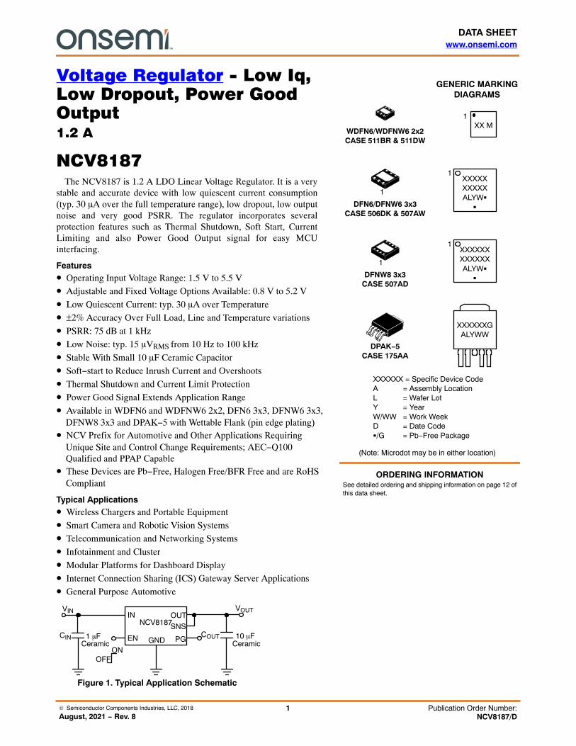
Figure 1. Typical Application Schematic
OUTIN
EN GND
SNS
PG
NCV8187
ONOFF
Ceramic10 �F
VOUT
COUTCIN 1 �FCeramic
VIN
See detailed ordering and shipping information on page 12 ofthis data sheet.
ORDERING INFORMATION
GENERIC MARKINGDIAGRAMS
WDFN6/WDFNW6 2x2CASE 511BR & 511DW
1
DFN6/DFNW6 3x3CASE 506DK & 507AW
DFNW8 3x3CASE 507AD
DPAK−5CASE 175AA
1
XXXXXXXXXXXXALYW�
�
1
XXXXXXXXXXALYW�
�
1
XXXXXXGALYWW
XXXXXX = Specific Device CodeA = Assembly LocationL = Wafer LotY = YearW/WW = Work WeekD = Date Code�/G = Pb−Free Package
(Note: Microdot may be in either location)
XX M1
NCV8187
www.onsemi.com2
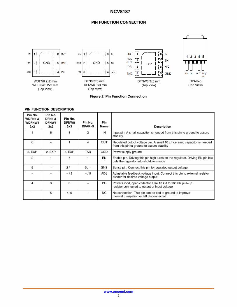
PIN FUNCTION CONNECTION
Figure 2. Pin Function Connection
WDFN6 2x2 mmWDFNW6 2x2 mm
(Top View)
DFN6 3x3 mm, DFNW6 3x3 mm
(Top View)
DFNW8 3x3 mm(Top View)
DPAK−5(Top View)
PIN FUNCTION DESCRIPTION
Pin No.WDFN6 &WDFNW6
2x2
Pin No.DFN6 &DFNW6
3x3
Pin No.DFNW8
3x3Pin No.DPAK−5
PinName Description
1 6 8 2 IN Input pin. A small capacitor is needed from this pin to ground to assurestability
6 4 1 4 OUT Regulated output voltage pin. A small 10 �F ceramic capacitor is neededfrom this pin to ground to assure stability
3, EXP 2, EXP 5, EXP TAB GND Power supply ground
2 1 7 1 EN Enable pin. Driving this pin high turns on the regulator. Driving EN pin lowputs the regulator into shutdown mode
5 − 2 / − 5 / − SNS Sense pin. Connect this pin to regulated output voltage
− − − / 2 − / 5 ADJ Adjustable feedback voltage input. Connect this pin to external resistordivider for desired voltage output
4 3 3 − PG Power Good, open collector. Use 10 k� to 100 k� pull−up resistor connected to output or input voltage
− 5 4, 6 − NC No connection. This pin can be tied to ground to improve thermal dissipation or left disconnected
NCV8187
www.onsemi.com3
ABSOLUTE MAXIMUM RATINGS
Ratings Symbol Value Unit
Input Voltage (Note 1) VIN −0.3 to 6 V
Enable Voltage VEN −0.3 to 6 V
Power Good Current IPG 30 mA
Power Good Voltage VPG −0.3 to 6 V
Output Voltage VOUT −0.3 to VIN + 0.3 (max. 5.5) V
Output Short Circuit Duration tSC Indefinite s
Maximum Junction Temperature TJ(MAX) 150 °C
Storage Temperature TSTG −55 to 150 °C
ESD Capability, Human Body Model (Note 2) ESDHBM 2000 V
ESD Capability, Machine Model (Note 2) ESDMM 200 V
Stresses exceeding those listed in the Maximum Ratings table may damage the device. If any of these limits are exceeded, device functionalityshould not be assumed, damage may occur and reliability may be affected.1. Refer to ELECTRICAL CHARACTERISTICS and APPLICATION INFORMATION for Safe Operating Area.2. This device series incorporates ESD protection and is tested by the following methods:
ESD Human Body Model tested per AEC−Q100−002 (EIA/JESD22−A114)ESD Machine Model tested per AEC−Q100−003 (EIA/JESD22−A115)
THERMAL CHARACTERISTICS
Rating Symbol Value Unit
THERMAL CHARACTERISTICS, WDFN6, 2x2, 0.65 PITCH PACKAGE
Thermal Resistance, Junction−to−Ambient (Note 3) R�JA 51 °C/W
Thermal Resistance, Junction−to−Case (top) R�JC(top) 142 °C/W
Thermal Resistance, Junction−to−Case (bottom) (Note 4) R�JC(bot) 7.8 °C/W
Thermal Resistance, Junction−to−Board R�JB 125 °C/W
Characterization Parameter, Junction−to−Top �JT 2.0 °C/W
Characterization Parameter, Junction−to−Board �JB 7.7 °C/W
THERMAL CHARACTERISTICS, DFN6 / DFNW6, 3x3, 0.95 PITCH PACKAGES
Thermal Resistance, Junction−to−Ambient (Note 3) R�JA 50 °C/W
Thermal Resistance, Junction−to−Case (top) R�JC(top) 142 °C/W
Thermal Resistance, Junction−to−Case (bottom) (Note 4) R�JC(bot) 7.9 °C/W
Thermal Resistance, Junction−to−Board R�JB 125 °C/W
Characterization Parameter, Junction−to−Top �JT 2.0 °C/W
Characterization Parameter, Junction−to−Board �JB 7.5 °C/W
3. The junction−to−ambient thermal resistance under natural convection is obtained in a simulation on a high−K board, following the JEDEC51.7guidelines with assumptions as above, in an environment described in JESD51−2a.
4. The junction−to−case (bottom) thermal resistance is obtained by simulating a cold plate test on the IC exposed pad. Test description canbe found in the ANSI SEMI standard G30−88.
NCV8187
www.onsemi.com4
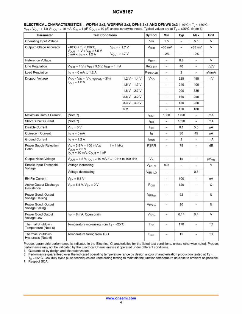
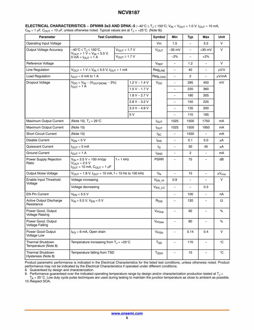
ELECTRICAL CHARACTERISTICS − WDFN6 2x2, WDFNW6 2x2, DFN6 3x3 AND DFNW6 3x3 (−40°C ≤ TJ ≤ 150°C; VIN = VOUT + 1.0 V; IOUT = 10 mA, CIN = 1 �F, COUT = 10 �F, unless otherwise noted. Typical values are at TJ = +25°C. (Note 6))
Parameter Test Conditions Symbol Min Typ Max Unit
Operating Input Voltage VIN 1.5 − 5.5 V
Output Voltage Accuracy −40°C ≤ TJ ≤ 150°C,VOUT +1 V < VIN < 5.5 V,0 mA < IOUT < 1.2 A
VOUT < 1.7 V VOUT −35 mV − +35 mV V
VOUT ≥ 1.7 V −2% − +2%
Reference Voltage VREF − 0.8 − V
Line Regulation VOUT + 1 V ≤ VIN ≤ 5.5 V, IOUT = 1 mA RegLINE − 40 − �V/V
Load Regulation IOUT = 0 mA to 1.2 A RegLOAD − 2 − �V/mA
Dropout Voltage VDO = VIN – (VOUT(NOM) – 3%)IOUT = 1.2 A
1.2 V – 1.4 V VDO − 325 495 mV
1.5 V – 1.7 V − 240 400
1.8 V – 2.7 V − 200 335
2.8 V – 3.2 V − 165 250
3.3 V – 4.9 V − 150 220
5 V − 120 180
Maximum Output Current (Note 7) IOUT 1300 1750 − mA
Short Circuit Current (Note 7) ISC − 1850 − mA
Disable Current VEN = 0 V IDIS − 0.1 5.0 �A
Quiescent Current IOUT = 0 mA IQ − 30 45 �A
Ground Current IOUT = 1.2 A IGND − 2 − mA
Power Supply Rejection Ratio
VIN = 3.5 V + 100 mVppVOUT = 2.5 VIOUT = 10 mA, COUT = 1 �F
f = 1 kHz PSRR − 75 − dB
Output Noise Voltage VOUT = 1.8 V, IOUT = 10 mA, f = 10 Hz to 100 kHz VN − 15 − �Vrms
Enable Input Threshold Voltage
Voltage increasing VEN_HI 0.9 − − V
Voltage decreasing VEN_LO − − 0.3
EN Pin Current VEN = 5.5 V − 100 − nA
Active Output Discharge Resistance
VIN = 5.5 V, VEN = 0 V RDIS − 120 − �
Power Good, Output Voltage Raising
VPGup − 92 − %
Power Good, Output Voltage Falling
VPGdw − 80 − %
Power Good Output Voltage Low
IPG = 6 mA, Open drain VPGlo − 0.14 0.4 V
Thermal Shutdown Temperature (Note 5)
Temperature increasing from TJ = +25°C TSD − 170 − °C
Thermal Shutdown Hysteresis (Note 5)
Temperature falling from TSD TSDH − 15 − °C
Product parametric performance is indicated in the Electrical Characteristics for the listed test conditions, unless otherwise noted. Productperformance may not be indicated by the Electrical Characteristics if operated under different conditions.5. Guaranteed by design and characterization.6. Performance guaranteed over the indicated operating temperature range by design and/or characterization production tested at TJ =
TA = 25�C. Low duty cycle pulse techniques are used during testing to maintain the junction temperature as close to ambient as possible.7. Respect SOA.
NCV8187
www.onsemi.com5
ELECTRICAL CHARACTERISTICS − DFNW8 3x3 AND DPAK−5 (−40°C ≤ TJ ≤ 150°C; VIN = VOUT + 1.0 V; IOUT = 10 mA, CIN = 1 �F, COUT = 10 �F, unless otherwise noted. Typical values are at TJ = +25°C. (Note 9))
Parameter Test Conditions Symbol Min Typ Max Unit
Operating Input Voltage VIN 1.5 − 5.5 V
Output Voltage Accuracy −40°C ≤ TJ ≤ 150°C,VOUT + 1 V < VIN < 5.5 V,0 mA < IOUT < 1 A
VOUT < 1.7 V VOUT −35 mV − +35 mV V
VOUT ≥ 1.7 V −2% − +2%
Reference Voltage VREF − 1.2 − V
Line Regulation VOUT + 1 V ≤ VIN ≤ 5.5 V, IOUT = 1 mA RegLINE − 40 − �V/V
Load Regulation IOUT = 0 mA to 1 A RegLOAD − 2 − �V/mA
Dropout Voltage VDO = VIN – (VOUT(NOM) – 3%)IOUT = 1 A
1.2 V – 1.4 V VDO − 295 450 mV
1.5 V – 1.7 V − 220 360
1.8 V – 2.7 V − 180 305
2.8 V – 3.2 V − 150 225
3.3 V – 4.9 V − 135 200
5 V − 110 165
Maximum Output Current (Note 10), TJ = 25°C IOUT 1025 1500 1750 mA
Maximum Output Current (Note 10) IOUT 1025 1500 1950 mA
Short Circuit Current (Note 10) ISC − 1550 − mA
Disable Current VEN = 0 V IDIS − 0.1 5.0 �A
Quiescent Current IOUT = 0 mA IQ − 30 45 �A
Ground Current IOUT = 1 A IGND − 2 − mA
Power Supply Rejection Ratio
VIN = 3.5 V + 100 mVppVOUT = 2.5 VIOUT = 10 mA, COUT = 1 �F
f = 1 kHz PSRR − 75 − dB
Output Noise Voltage VOUT = 1.8 V, IOUT = 10 mA, f = 10 Hz to 100 kHz VN − 15 − �Vrms
Enable Input Threshold Voltage
Voltage increasing VEN_HI 0.9 − − V
Voltage decreasing VEN_LO − − 0.3
EN Pin Current VEN = 5.5 V − 100 − nA
Active Output Discharge Resistance
VIN = 5.5 V, VEN = 0 V RDIS − 120 − �
Power Good, Output Voltage Raising
VPGup − 92 − %
Power Good, Output Voltage Falling
VPGdw − 80 − %
Power Good Output Voltage Low
IPG = 6 mA, Open drain VPGlo − 0.14 0.4 V
Thermal Shutdown Temperature (Note 8)
Temperature increasing from TJ = +25°C TSD − 170 − °C
Thermal Shutdown Hysteresis (Note 8)
Temperature falling from TSD TSDH − 15 − °C
Product parametric performance is indicated in the Electrical Characteristics for the listed test conditions, unless otherwise noted. Productperformance may not be indicated by the Electrical Characteristics if operated under different conditions.8. Guaranteed by design and characterization.9. Performance guaranteed over the indicated operating temperature range by design and/or characterization production tested at TJ =
TA = 25�C. Low duty cycle pulse techniques are used during testing to maintain the junction temperature as close to ambient as possible.10.Respect SOA.
NCV8187
www.onsemi.com6
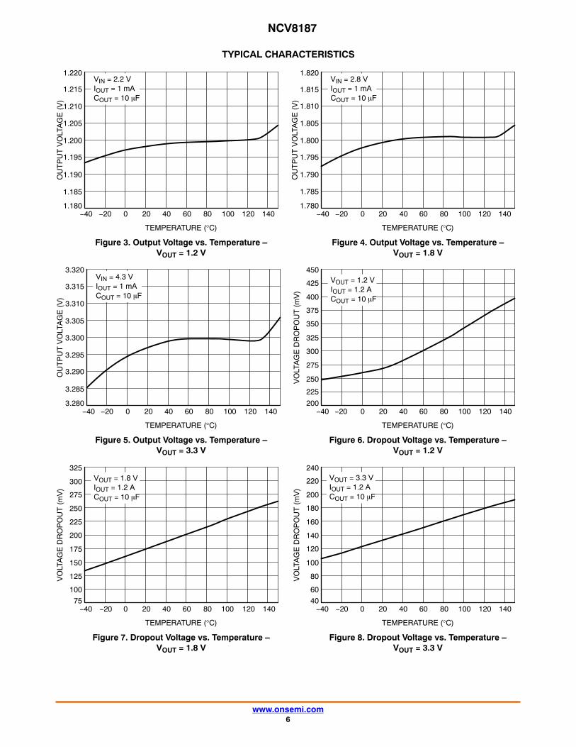
TYPICAL CHARACTERISTICS
Figure 3. Output Voltage vs. Temperature –VOUT = 1.2 V
Figure 4. Output Voltage vs. Temperature –VOUT = 1.8 V
TEMPERATURE (°C) TEMPERATURE (°C)
1201006040200−20−401.180
1.185
1.190
1.200
1.205
1.210
1.215
1.220
1201008060200−20−401.780
1.785
1.790
1.795
1.800
1.805
1.815
1.820
Figure 5. Output Voltage vs. Temperature –VOUT = 3.3 V
Figure 6. Dropout Voltage vs. Temperature –VOUT = 1.2 V
TEMPERATURE (°C) TEMPERATURE (°C)
1201008060200−20−403.280
3.285
3.290
3.300
3.305
3.310
3.315
3.320
1201008060200−20−40200
225
275
300
350
375
400
450
Figure 7. Dropout Voltage vs. Temperature –VOUT = 1.8 V
Figure 8. Dropout Voltage vs. Temperature –VOUT = 3.3 V
TEMPERATURE (°C) TEMPERATURE (°C)
1201008060400−20−4075
100
150
175
200
250
275
325
1201008060400−20−4040
60
80
120
160
180
200
240
OU
TP
UT
VO
LTA
GE
(V
)
OU
TP
UT
VO
LTA
GE
(V
)
OU
TP
UT
VO
LTA
GE
(V
)
VO
LTA
GE
DR
OP
OU
T (
mV
)
VO
LTA
GE
DR
OP
OU
T (
mV
)
VO
LTA
GE
DR
OP
OU
T (
mV
)
80 140
1.195
VIN = 2.2 VIOUT = 1 mACOUT = 10 �F
VIN = 2.8 VIOUT = 1 mACOUT = 10 �F
40 140
1.810
VOUT = 1.2 VIOUT = 1.2 ACOUT = 10 �F
VIN = 4.3 VIOUT = 1 mACOUT = 10 �F
40 140
3.295
40 140
250
325
425
20 140
100
140
220 VOUT = 3.3 VIOUT = 1.2 ACOUT = 10 �F
VOUT = 1.8 VIOUT = 1.2 ACOUT = 10 �F
20 140
125
225
300
NCV8187
www.onsemi.com7
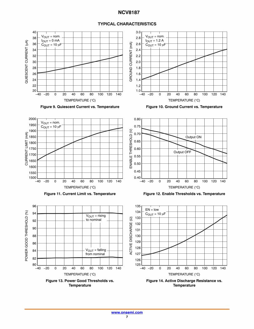
TYPICAL CHARACTERISTICS
Figure 9. Quiescent Current vs. Temperature Figure 10. Ground Current vs. Temperature
TEMPERATURE (°C) TEMPERATURE (°C)
1201008060200−20−4020
22
26
28
30
34
38
40
1201008060400−20−401.01.2
1.6
1.8
2.2
2.4
2.6
3.0
Figure 11. Current Limit vs. Temperature Figure 12. Enable Thresholds vs. Temperature
TEMPERATURE (°C) TEMPERATURE (°C)
1201008060400−20−4015001550
1650
1700
1800
1850
1950
2000
1201008060200−20−400.40
0.45
0.50
0.55
0.60
0.70
0.75
0.80
Figure 13. Power Good Thresholds vs.Temperature
Figure 14. Active Discharge Resistance vs.Temperature
TEMPERATURE (°C) TEMPERATURE (°C)
1401008060400−20−4080
82
84
86
88
92
94
96
1201008060400−20−40125126
128
129
131
132
133
135
QU
IES
CE
NT
CU
RR
EN
T (�A
)
GR
OU
ND
CU
RR
EN
T (
mA
)
CU
RR
EN
T L
IMIT
(m
A)
EN
AB
LE T
HR
ES
HO
LD (
V)
PO
WE
R G
OO
D T
HR
ES
HO
LD (
%)
AC
TIV
E D
ISC
HA
RG
E (�
)
VOUT = nom.IOUT = 0 mACOUT = 10 �F
24
32
36
40 140 20 140
1.4
2.0
2.8 VOUT = nom.IOUT = 1.2 ACOUT = 10 �F
Output ON
Output OFF
40 140
0.65
VOUT = nom.COUT = 10 �F
20 140
1600
1750
1900
VOUT = risingto nominal
90
VOUT = fallingfrom nominal
20 120
127
130
134
20 140
EN = lowCOUT = 10 �F
NCV8187
www.onsemi.com8
TYPICAL CHARACTERISTICS
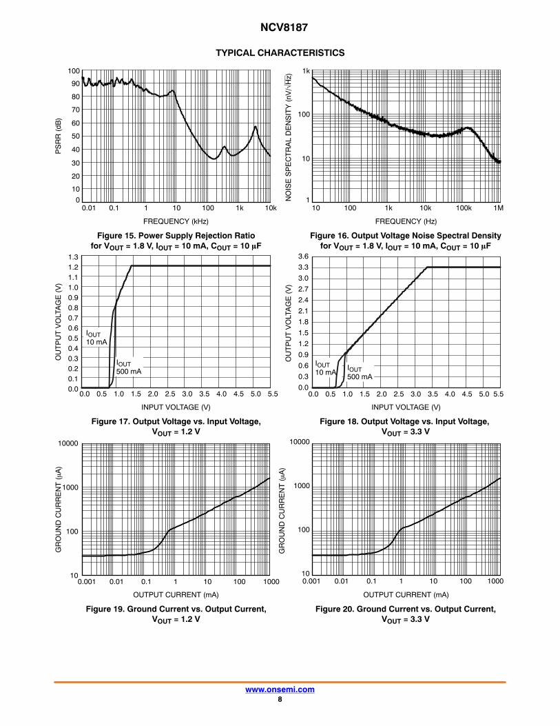
Figure 15. Power Supply Rejection Ratiofor VOUT = 1.8 V, IOUT = 10 mA, COUT = 10 �F
Figure 16. Output Voltage Noise Spectral Densityfor VOUT = 1.8 V, IOUT = 10 mA, COUT = 10 �F
FREQUENCY (kHz) FREQUENCY (Hz)
1k10010 10k10.10.010
10
30
40
60
70
90
100
100k10k1k 1M100101
10
100
1k
PS
RR
(dB
)
NO
ISE
SP
EC
TR
AL
DE
NS
ITY
(nV
/√H
z)
80
50
20
Figure 17. Output Voltage vs. Input Voltage,VOUT = 1.2 V
Figure 18. Output Voltage vs. Input Voltage, VOUT = 3.3 V
INPUT VOLTAGE (V) INPUT VOLTAGE (V)
OU
TP
UT
VO
LTA
GE
(V
)
OU
TP
UT
VO
LTA
GE
(V
)
0.00.10.20.30.40.50.60.70.80.91.01.11.21.3
0.0 0.5 1.0 1.5 2.0 2.5 3.0 3.5 4.0 4.5 5.0 5.5
IOUT10 mA
IOUT500 mA
0.0
0.3
0.6
0.9
1.2
1.5
1.8
2.1
2.4
2.7
3.0
3.3
3.6
0.0 0.5 1.0 1.5 2.0 2.5 3.0 3.5 4.0 4.5 5.0 5.5
IOUT10 mA
IOUT500 mA
Figure 19. Ground Current vs. Output Current,VOUT = 1.2 V
Figure 20. Ground Current vs. Output Current,VOUT = 3.3 V
OUTPUT CURRENT (mA) OUTPUT CURRENT (mA)
GR
OU
ND
CU
RR
EN
T (�A
)
GR
OU
ND
CU
RR
EN
T (�A
)
10
100
1000
10000
0.001 0.01 0.1 1 10 100 100010
100
1000
10000
0.001 0.01 0.1 1 10 100 1000
NCV8187
www.onsemi.com9
TYPICAL CHARACTERISTICS
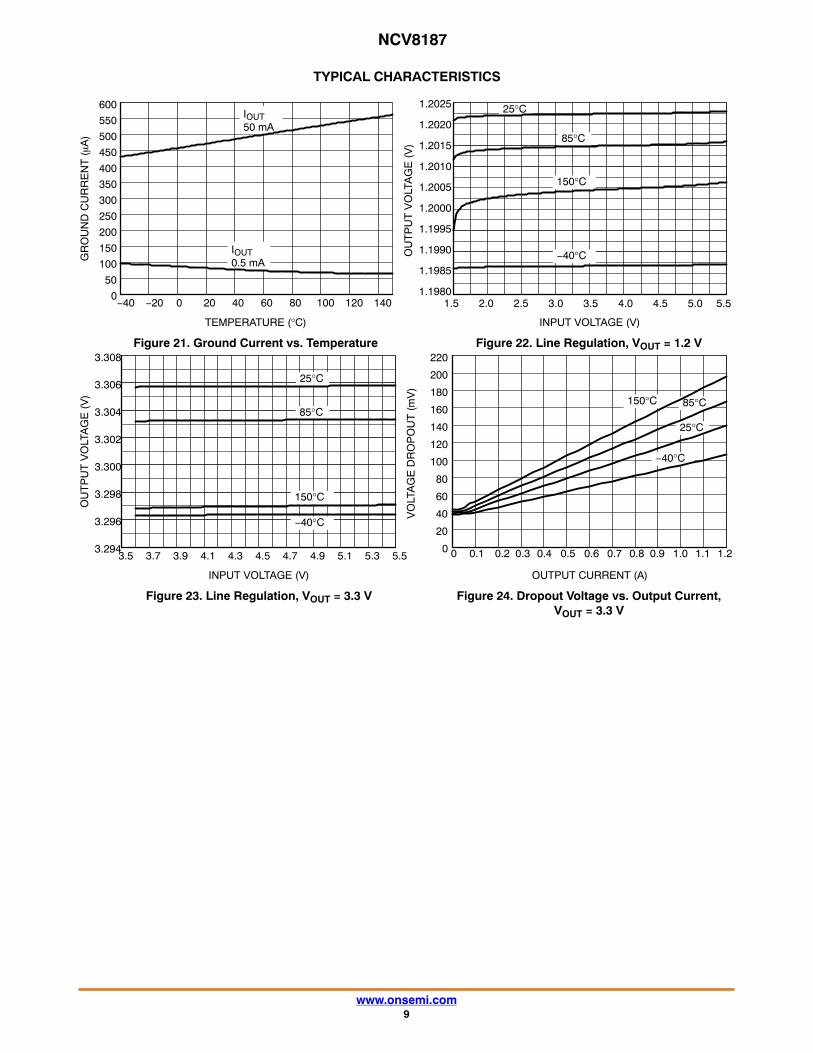
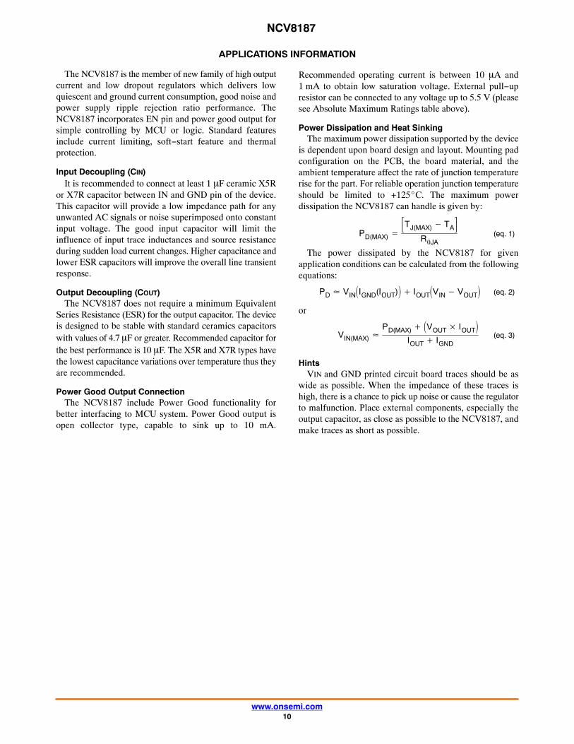
Figure 21. Ground Current vs. Temperature Figure 22. Line Regulation, VOUT = 1.2 V
TEMPERATURE (°C) INPUT VOLTAGE (V)
GR
OU
ND
CU
RR
EN
T (�A
)
OU
TP
UT
VO
LTA
GE
(V
)
0
50
100
150
200
250
300
350
400
450
500
550
600
−40 −20 0 20 40 60 80 100 120 140
IOUT0.5 mA
IOUT50 mA
1.1980
1.1985
1.1990
1.1995
1.2000
1.2005
1.2010
1.2015
1.2020
1.2025
1.5 2.0 2.5 3.0 3.5 4.0 4.5 5.0 5.5
−40°C
25°C
85°C
150°C
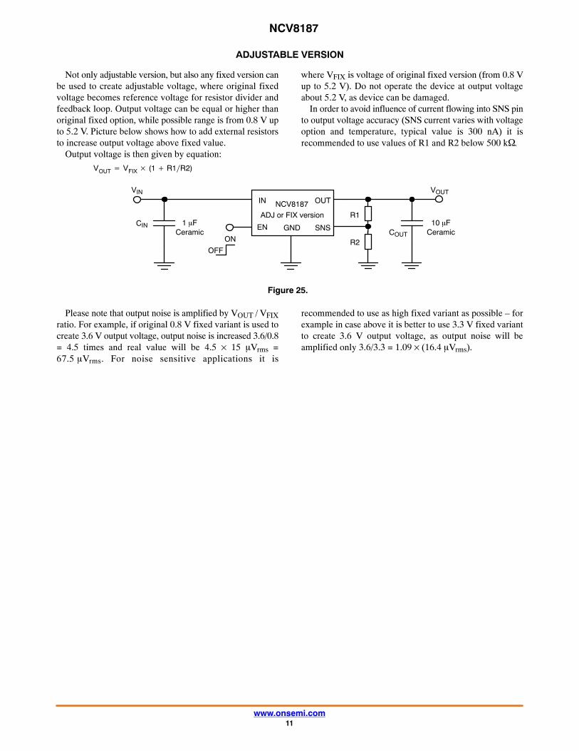
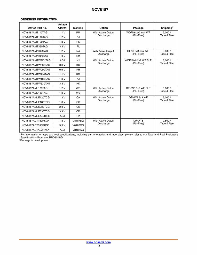
Figure 23. Line Regulation, VOUT = 3.3 V Figure 24. Dropout Voltage vs. Output Current,VOUT = 3.3 V
INPUT VOLTAGE (V) OUTPUT CURRENT (A)
OU
TP
UT
VO
LTA
GE
(V
)
VO
LTA
GE
DR
OP
OU
T (
mV
)
3.294
3.296
3.298
3.300
3.302
3.304
3.306
3.308
3.5 3.7 3.9 4.1 4.3 4.5 4.7 4.9 5.1 5.3 5.5
−40°C
25°C
85°C
150°C
0
20
40
60
80
100
120
140
160
180
200
220
−40°C
25°C
85°C150°C
1.00.9 1.21.10.80.70 0.1 0.2 0.3 0.4 0.5 0.6
NCV8187
www.onsemi.com10
APPLICATIONS INFORMATION
The NCV8187 is the member of new family of high outputcurrent and low dropout regulators which delivers lowquiescent and ground current consumption, good noise andpower supply ripple rejection ratio performance. TheNCV8187 incorporates EN pin and power good output forsimple controlling by MCU or logic. Standard featuresinclude current limiting, soft−start feature and thermalprotection.
Input Decoupling (CIN)It is recommended to connect at least 1 �F ceramic X5R
or X7R capacitor between IN and GND pin of the device.This capacitor will provide a low impedance path for anyunwanted AC signals or noise superimposed onto constantinput voltage. The good input capacitor will limit theinfluence of input trace inductances and source resistanceduring sudden load current changes. Higher capacitance andlower ESR capacitors will improve the overall line transientresponse.
Output Decoupling (COUT)The NCV8187 does not require a minimum Equivalent
Series Resistance (ESR) for the output capacitor. The deviceis designed to be stable with standard ceramics capacitorswith values of 4.7 �F or greater. Recommended capacitor forthe best performance is 10 �F. The X5R and X7R types havethe lowest capacitance variations over temperature thus theyare recommended.
Power Good Output ConnectionThe NCV8187 include Power Good functionality for
better interfacing to MCU system. Power Good output isopen collector type, capable to sink up to 10 mA.
Recommended operating current is between 10 �A and1 mA to obtain low saturation voltage. External pull−upresistor can be connected to any voltage up to 5.5 V (pleasesee Absolute Maximum Ratings table above).
Power Dissipation and Heat SinkingThe maximum power dissipation supported by the device
is dependent upon board design and layout. Mounting padconfiguration on the PCB, the board material, and theambient temperature affect the rate of junction temperaturerise for the part. For reliable operation junction temperatureshould be limited to +125�C. The maximum powerdissipation the NCV8187 can handle is given by:
PD(MAX) ��TJ(MAX) � TA
�R�JA
(eq. 1)
The power dissipated by the NCV8187 for givenapplication conditions can be calculated from the followingequations:
PD � VIN�IGND(IOUT)� IOUT
�VIN � VOUT� (eq. 2)
or
VIN(MAX) �PD(MAX) �VOUT IOUT
�IOUT IGND
(eq. 3)
HintsVIN and GND printed circuit board traces should be as
wide as possible. When the impedance of these traces ishigh, there is a chance to pick up noise or cause the regulatorto malfunction. Place external components, especially theoutput capacitor, as close as possible to the NCV8187, andmake traces as short as possible.
NCV8187
www.onsemi.com11
ADJUSTABLE VERSION
Not only adjustable version, but also any fixed version canbe used to create adjustable voltage, where original fixedvoltage becomes reference voltage for resistor divider andfeedback loop. Output voltage can be equal or higher thanoriginal fixed option, while possible range is from 0.8 V upto 5.2 V. Picture below shows how to add external resistorsto increase output voltage above fixed value.
Output voltage is then given by equation:
VOUT � VFIX (1 R1�R2)
where VFIX is voltage of original fixed version (from 0.8 Vup to 5.2 V). Do not operate the device at output voltageabout 5.2 V, as device can be damaged.
In order to avoid influence of current flowing into SNS pinto output voltage accuracy (SNS current varies with voltageoption and temperature, typical value is 300 nA) it isrecommended to use values of R1 and R2 below 500 k�.
Figure 25.
VIN
CIN
OFF
ON
1 �FCeramic
IN
EN
OUT
SNSGND
NCV8187ADJ or FIX version R1
R2COUT
10 �FCeramic
VOUT
Please note that output noise is amplified by VOUT / VFIXratio. For example, if original 0.8 V fixed variant is used tocreate 3.6 V output voltage, output noise is increased 3.6/0.8= 4.5 times and real value will be 4.5 × 15 �Vrms =67.5��Vrms. For noise sensitive applications it is
recommended to use as high fixed variant as possible – forexample in case above it is better to use 3.3 V fixed variantto create 3.6 V output voltage, as output noise will beamplified only 3.6/3.3 = 1.09 × (16.4 �Vrms).
NCV8187
www.onsemi.com12
ORDERING INFORMATION
Device Part No.VoltageOption Marking Option Package Shipping†
NCV8187AMT110TAG 1.1 V PM With Active OutputDischarge
WDFN6 2x2 non WF(Pb−Free)
3,000 / Tape & Reel
NCV8187AMT120TAG 1.2 V PJ
NCV8187AMT180TAG 1.8 V PK
NCV8187AMT330TAG 3.3 V PL
NCV8187AMN120TAG 1.2 V NA With Active Output Discharge
DFN6 3x3 non WF (Pb−Free)
3,000 / Tape & Reel
NCV8187AMN180TAG 1.8 V NH
NCV8187AMTWADJTAG ADJ K2 With Active OutputDischarge
WDFNW6 2x2 WF SLP(Pb−Free)
3,000 / Tape & Reel
NCV8187AMTW080TAG 0.8 V KG
NCV8187AMTW090TAG 0.9 V KH
NCV8187AMTW110TAG 1.1 V KM
NCV8187AMTW180TAG 1.8 V KJ
NCV8187AMTW330TAG 3.3 V KK
NCV8187AML120TAG 1.2 V WD With Active OutputDischarge
DFNW6 3x3 WF SLP(Pb−Free)
3,000 / Tape & Reel
NCV8187AML180TAG 1.8 V WE
NCV8187AMLE120TCG 1.2 V CA With Active OutputDischarge
DFNW8 3x3 WF(Pb−Free)
3,000 / Tape & Reel
NCV8187AMLE180TCG 1.8 V CC
NCV8187AMLE280TCG 2.8 V CE
NCV8187AMLE330TCG 3.3 V CD
NCV8187AMLEADJTCG ADJ C2
NCV8187ADT180RKG* 1.8 V V8187BG With Active OutputDischarge
DPAK−5(Pb−Free)
2,500 / Tape & Reel
NCV8187ADT330RKG* 3.3 V V8187CG
NCV8187ADTADJRKG* ADJ V8187AG
†For information on tape and reel specifications, including part orientation and tape sizes, please refer to our Tape and Reel PackagingSpecifications Brochure, BRD8011/D.
*Package in development.
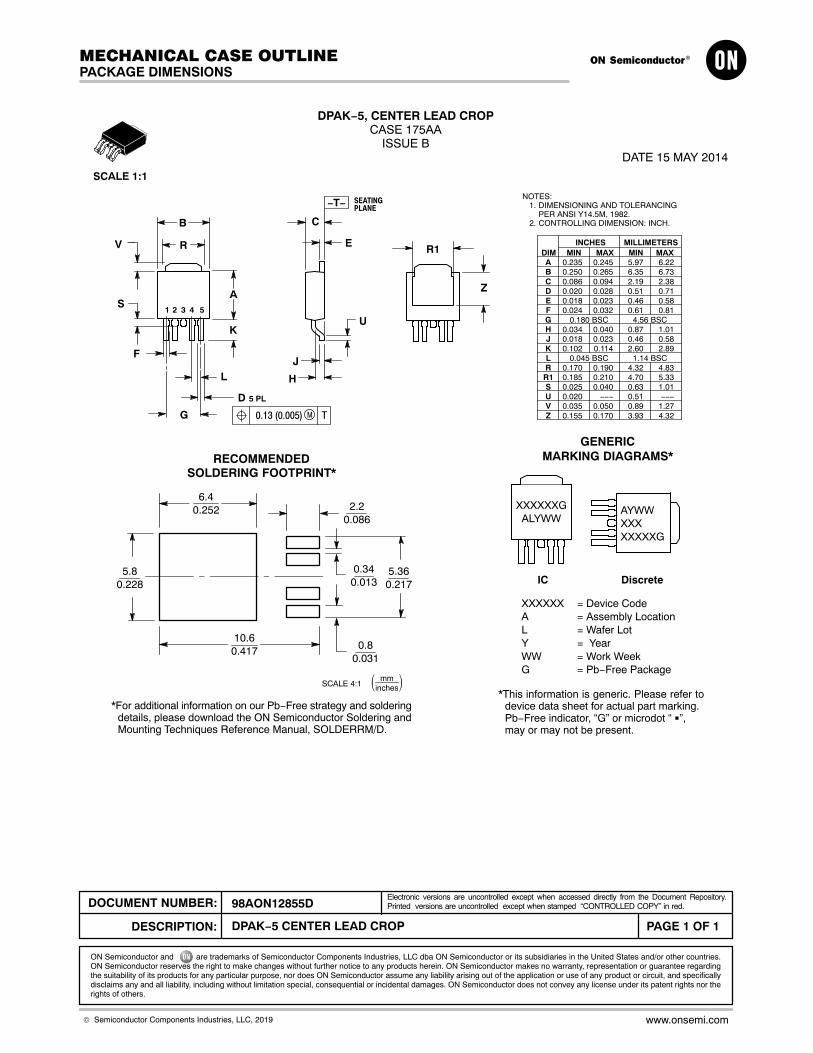
DPAK−5, CENTER LEAD CROPCASE 175AA
ISSUE BDATE 15 MAY 2014
D
A
K
B
RV
S
F
L
G
5 PL
M0.13 (0.005) T
E
C
U
J
H
−T− SEATINGPLANE
Z
DIM MIN MAX MIN MAXMILLIMETERSINCHES
A 0.235 0.245 5.97 6.22B 0.250 0.265 6.35 6.73C 0.086 0.094 2.19 2.38D 0.020 0.028 0.51 0.71E 0.018 0.023 0.46 0.58F 0.024 0.032 0.61 0.81G 0.180 BSC 4.56 BSCH 0.034 0.040 0.87 1.01J 0.018 0.023 0.46 0.58K 0.102 0.114 2.60 2.89L 0.045 BSC 1.14 BSCR 0.170 0.190 4.32 4.83
S 0.025 0.040 0.63 1.01U 0.020 −−− 0.51 −−−V 0.035 0.050 0.89 1.27Z 0.155 0.170 3.93 4.32
NOTES:1. DIMENSIONING AND TOLERANCING
PER ANSI Y14.5M, 1982.2. CONTROLLING DIMENSION: INCH.
XXXXXXGALYWW
R1 0.185 0.210 4.70 5.33
R1
GENERICMARKING DIAGRAMS*
1 2 3 4 5
6.40.252
0.80.031
10.60.417
5.80.228
SCALE 4:1 � mminches
�
0.340.013
5.360.217
2.20.086
*This information is generic. Please refer todevice data sheet for actual part marking.Pb−Free indicator, “G” or microdot “ �”,may or may not be present.
SCALE 1:1
*For additional information on our Pb−Free strategy and solderingdetails, please download the ON Semiconductor Soldering andMounting Techniques Reference Manual, SOLDERRM/D.
SOLDERING FOOTPRINT*RECOMMENDED
AYWWXXXXXXXXG
DiscreteIC
XXXXXX = Device CodeA = Assembly LocationL = Wafer LotY = YearWW = Work WeekG = Pb−Free Package
MECHANICAL CASE OUTLINE
PACKAGE DIMENSIONS
ON Semiconductor and are trademarks of Semiconductor Components Industries, LLC dba ON Semiconductor or its subsidiaries in the United States and/or other countries.ON Semiconductor reserves the right to make changes without further notice to any products herein. ON Semiconductor makes no warranty, representation or guarantee regardingthe suitability of its products for any particular purpose, nor does ON Semiconductor assume any liability arising out of the application or use of any product or circuit, and specificallydisclaims any and all liability, including without limitation special, consequential or incidental damages. ON Semiconductor does not convey any license under its patent rights nor therights of others.
98AON12855DDOCUMENT NUMBER:
DESCRIPTION:
Electronic versions are uncontrolled except when accessed directly from the Document Repository.Printed versions are uncontrolled except when stamped “CONTROLLED COPY” in red.
PAGE 1 OF 1DPAK−5 CENTER LEAD CROP
© Semiconductor Components Industries, LLC, 2019 www.onsemi.com
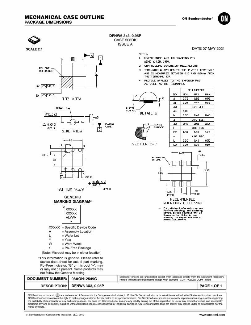
DFNW6 3x3, 0.95PCASE 506DK
ISSUE ADATE 07 MAY 2021SCALE 2:1
GENERICMARKING DIAGRAM*
XXXXX = Specific Device CodeA = Assembly LocationL = Wafer LotY = YearW = Work Week� = Pb−Free Package
1
XXXXXXXXXXALYW�
�
(Note: Microdot may be in either location)
*This information is generic. Please refer todevice data sheet for actual part marking.Pb−Free indicator, “G” or microdot “�”, mayor may not be present. Some products maynot follow the Generic Marking.
MECHANICAL CASE OUTLINE
PACKAGE DIMENSIONS
ON Semiconductor and are trademarks of Semiconductor Components Industries, LLC dba ON Semiconductor or its subsidiaries in the United States and/or other countries.ON Semiconductor reserves the right to make changes without further notice to any products herein. ON Semiconductor makes no warranty, representation or guarantee regardingthe suitability of its products for any particular purpose, nor does ON Semiconductor assume any liability arising out of the application or use of any product or circuit, and specificallydisclaims any and all liability, including without limitation special, consequential or incidental damages. ON Semiconductor does not convey any license under its patent rights nor therights of others.
98AON12549GDOCUMENT NUMBER:
DESCRIPTION:
Electronic versions are uncontrolled except when accessed directly from the Document Repository.Printed versions are uncontrolled except when stamped “CONTROLLED COPY” in red.
PAGE 1 OF 1DFNW6 3X3, 0.95P
© Semiconductor Components Industries, LLC, 2019 www.onsemi.com
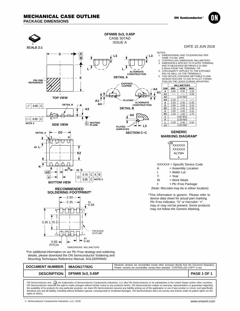
DFNW8 3x3, 0.65PCASE 507AD
ISSUE ADATE 15 JUN 2018SCALE 2:1
NOTES:1. DIMENSIONING AND TOLERANCING PER
ASME Y14.5M, 1994.2. CONTROLLING DIMENSION: MILLIMETERS.3. DIMENSION b APPLIES TO PLATED TERMINAL
AND IS MEASURED BETWEEN 0.15 AND0.30mm FROM THE TERMINAL TIP.
4. COPLANARITY APPLIES TO THE EXPOSEDPAD AS WELL AS THE TERMINALS.
5. THIS DEVICE CONTAINS WETTABLE FLANKDESIGN FEATURE TO AID IN FILLET FORMA-TION ON THE LEADS DURING MOUNTING.
ÉÉÉÉÉÉÉÉÉÉÉÉ
AB
E
D
D2
E2
BOTTOM VIEW
b
e
8X
0.10 B
0.05
AC
C NOTE 3
PIN ONEREFERENCE
TOP VIEW
AA3
0.05 C
0.05 C
C SEATINGPLANESIDE VIEW
L8X
1 4
58
1
*For additional information on our Pb−Free strategy and solderingdetails, please download the ON Semiconductor Soldering andMounting Techniques Reference Manual, SOLDERRM/D.
RECOMMENDED
DETAIL B
DETAIL A
NOTE 4
e/2
GENERICMARKING DIAGRAM*
XXXXXX = Specific Device CodeA = Assembly LocationL = Wafer LotY = YearW = Work Week� = Pb−Free Package
XXXXXXXXXXXXALYW�
�
1
(Note: Microdot may be in either location)SOLDERING FOOTPRINT*
DIM MIN NOMMILLIMETERS
A 0.80 0.90A1 −−− −−−
b 0.25 0.30DD2 2.30 2.40E
E2 1.55 1.65e 0.65 BSC
L 0.30 0.40
A3 0.20 REF
2.90 3.00
K
A4
L3
MAX
2.90 3.00
1.000.05
0.35
2.50
1.75
0.50
3.10
3.10
ALTERNATECONSTRUCTION
DETAIL A
L3
SECTION C−C
PLATED
A4
SURFACESL3
L3
L
DETAIL B
PLATING
EXPOSED
ALTERNATECONSTRUCTION
COPPER
A4A1
A4A1
L
CC
PACKAGEOUTLINE1 4
8 5
8X0.58
2.50
1.75
0.400.65PITCH
3.30
8X
DIMENSIONS: MILLIMETERS
2.35
K
0.28 REF
0.05 REF
*This information is generic. Please refer todevice data sheet for actual part marking.Pb−Free indicator, “G” or microdot “ �”,may or may not be present. Some productsmay not follow the Generic Marking.
0.10 −−− −−−
MECHANICAL CASE OUTLINE
PACKAGE DIMENSIONS
ON Semiconductor and are trademarks of Semiconductor Components Industries, LLC dba ON Semiconductor or its subsidiaries in the United States and/or other countries.ON Semiconductor reserves the right to make changes without further notice to any products herein. ON Semiconductor makes no warranty, representation or guarantee regardingthe suitability of its products for any particular purpose, nor does ON Semiconductor assume any liability arising out of the application or use of any product or circuit, and specificallydisclaims any and all liability, including without limitation special, consequential or incidental damages. ON Semiconductor does not convey any license under its patent rights nor therights of others.
98AON17792GDOCUMENT NUMBER:
DESCRIPTION:
Electronic versions are uncontrolled except when accessed directly from the Document Repository.Printed versions are uncontrolled except when stamped “CONTROLLED COPY” in red.
PAGE 1 OF 1DFNW8 3x3, 0.65P
© Semiconductor Components Industries, LLC, 2018 www.onsemi.com
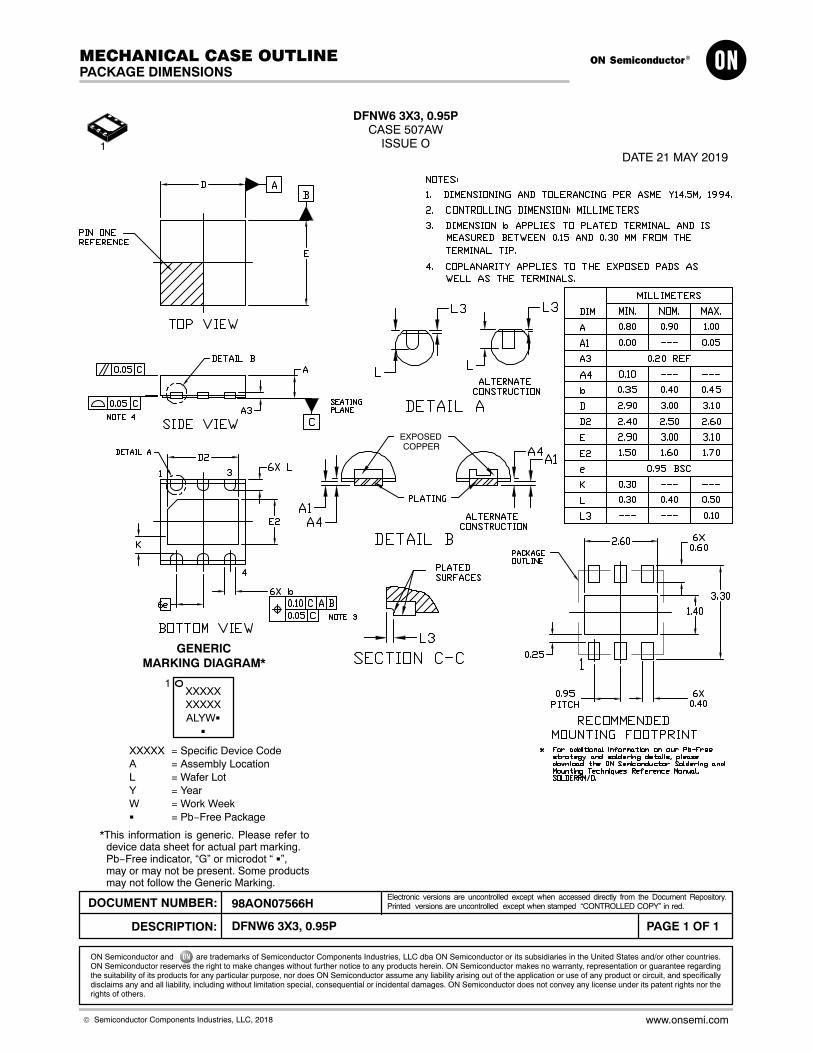
DFNW6 3X3, 0.95PCASE 507AW
ISSUE ODATE 21 MAY 2019
GENERICMARKING DIAGRAM*
XXXXX = Specific Device CodeA = Assembly LocationL = Wafer LotY = YearW = Work Week� = Pb−Free Package
XXXXXXXXXXALYW�
�
1
*This information is generic. Please refer todevice data sheet for actual part marking.Pb−Free indicator, “G” or microdot “ �”,may or may not be present. Some productsmay not follow the Generic Marking.
EXPOSED COPPER
1
MECHANICAL CASE OUTLINE
PACKAGE DIMENSIONS
ON Semiconductor and are trademarks of Semiconductor Components Industries, LLC dba ON Semiconductor or its subsidiaries in the United States and/or other countries.ON Semiconductor reserves the right to make changes without further notice to any products herein. ON Semiconductor makes no warranty, representation or guarantee regardingthe suitability of its products for any particular purpose, nor does ON Semiconductor assume any liability arising out of the application or use of any product or circuit, and specificallydisclaims any and all liability, including without limitation special, consequential or incidental damages. ON Semiconductor does not convey any license under its patent rights nor therights of others.
98AON07566HDOCUMENT NUMBER:
DESCRIPTION:
Electronic versions are uncontrolled except when accessed directly from the Document Repository.Printed versions are uncontrolled except when stamped “CONTROLLED COPY” in red.
PAGE 1 OF 1DFNW6 3X3, 0.95P
© Semiconductor Components Industries, LLC, 2018 www.onsemi.com
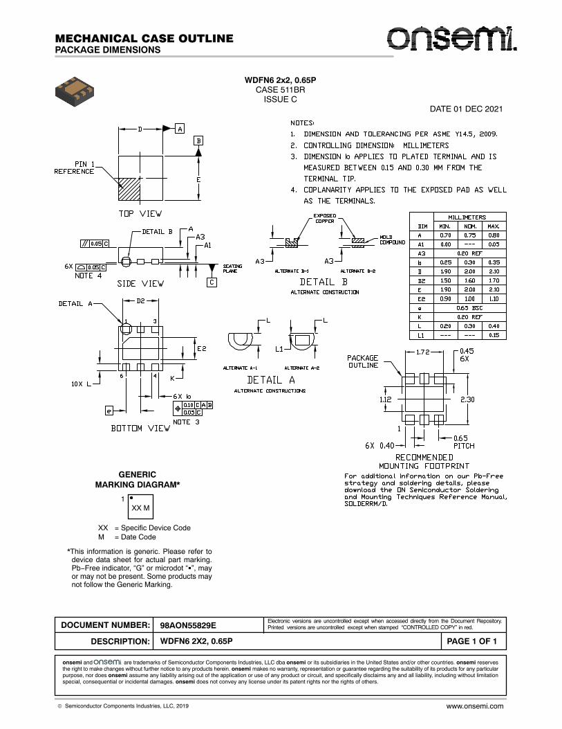
WDFN6 2x2, 0.65PCASE 511BR
ISSUE CDATE 01 DEC 2021
GENERICMARKING DIAGRAM*
XX = Specific Device CodeM = Date Code
XX M1
*This information is generic. Please refer todevice data sheet for actual part marking.Pb−Free indicator, “G” or microdot “�”, mayor may not be present. Some products maynot follow the Generic Marking.
MECHANICAL CASE OUTLINE
PACKAGE DIMENSIONS
98AON55829EDOCUMENT NUMBER:
DESCRIPTION:
Electronic versions are uncontrolled except when accessed directly from the Document Repository.Printed versions are uncontrolled except when stamped “CONTROLLED COPY” in red.
PAGE 1 OF 1WDFN6 2X2, 0.65P
onsemi and are trademarks of Semiconductor Components Industries, LLC dba onsemi or its subsidiaries in the United States and/or other countries. onsemi reservesthe right to make changes without further notice to any products herein. onsemi makes no warranty, representation or guarantee regarding the suitability of its products for any particularpurpose, nor does onsemi assume any liability arising out of the application or use of any product or circuit, and specifically disclaims any and all liability, including without limitationspecial, consequential or incidental damages. onsemi does not convey any license under its patent rights nor the rights of others.
© Semiconductor Components Industries, LLC, 2019 www.onsemi.com
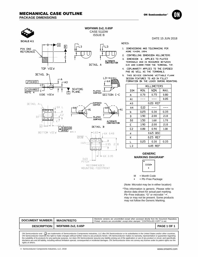
WDFNW6 2x2, 0.65PCASE 511DW
ISSUE BDATE 15 JUN 2018
M = Month Code� = Pb−Free Package
*This information is generic. Please refer todevice data sheet for actual part marking.Pb−Free indicator, “G” or microdot “ �”,may or may not be present. Some productsmay not follow the Generic Marking.
GENERICMARKING DIAGRAM*
XXM�
�
(Note: Microdot may be in either location)
SCALE 4:1
MECHANICAL CASE OUTLINE
PACKAGE DIMENSIONS
ON Semiconductor and are trademarks of Semiconductor Components Industries, LLC dba ON Semiconductor or its subsidiaries in the United States and/or other countries.ON Semiconductor reserves the right to make changes without further notice to any products herein. ON Semiconductor makes no warranty, representation or guarantee regardingthe suitability of its products for any particular purpose, nor does ON Semiconductor assume any liability arising out of the application or use of any product or circuit, and specificallydisclaims any and all liability, including without limitation special, consequential or incidental damages. ON Semiconductor does not convey any license under its patent rights nor therights of others.
98AON79327GDOCUMENT NUMBER:
DESCRIPTION:
Electronic versions are uncontrolled except when accessed directly from the Document Repository.Printed versions are uncontrolled except when stamped “CONTROLLED COPY” in red.
PAGE 1 OF 1WDFNW6 2x2, 0.65P
© Semiconductor Components Industries, LLC, 2018 www.onsemi.com
onsemi, , and other names, marks, and brands are registered and/or common law trademarks of Semiconductor Components Industries, LLC dba “onsemi” or its affiliatesand/or subsidiaries in the United States and/or other countries. onsemi owns the rights to a number of patents, trademarks, copyrights, trade secrets, and other intellectual property.A listing of onsemi’s product/patent coverage may be accessed at www.onsemi.com/site/pdf/Patent−Marking.pdf. onsemi reserves the right to make changes at any time to anyproducts or information herein, without notice. The information herein is provided “as−is” and onsemi makes no warranty, representation or guarantee regarding the accuracy of theinformation, product features, availability, functionality, or suitability of its products for any particular purpose, nor does onsemi assume any liability arising out of the application or useof any product or circuit, and specifically disclaims any and all liability, including without limitation special, consequential or incidental damages. Buyer is responsible for its productsand applications using onsemi products, including compliance with all laws, regulations and safety requirements or standards, regardless of any support or applications informationprovided by onsemi. “Typical” parameters which may be provided in onsemi data sheets and/or specifications can and do vary in different applications and actual performance mayvary over time. All operating parameters, including “Typicals” must be validated for each customer application by customer’s technical experts. onsemi does not convey any licenseunder any of its intellectual property rights nor the rights of others. onsemi products are not designed, intended, or authorized for use as a critical component in life support systemsor any FDA Class 3 medical devices or medical devices with a same or similar classification in a foreign jurisdiction or any devices intended for implantation in the human body. ShouldBuyer purchase or use onsemi products for any such unintended or unauthorized application, Buyer shall indemnify and hold onsemi and its officers, employees, subsidiaries, affiliates,and distributors harmless against all claims, costs, damages, and expenses, and reasonable attorney fees arising out of, directly or indirectly, any claim of personal injury or deathassociated with such unintended or unauthorized use, even if such claim alleges that onsemi was negligent regarding the design or manufacture of the part. onsemi is an EqualOpportunity/Affirmative Action Employer. This literature is subject to all applicable copyright laws and is not for resale in any manner.
PUBLICATION ORDERING INFORMATIONTECHNICAL SUPPORTNorth American Technical Support:Voice Mail: 1 800−282−9855 Toll Free USA/CanadaPhone: 011 421 33 790 2910
LITERATURE FULFILLMENT:Email Requests to: [email protected]
onsemi Website: www.onsemi.com
Europe, Middle East and Africa Technical Support:Phone: 00421 33 790 2910For additional information, please contact your local Sales Representative
◊