neotec semiconductor ltd. - crystalfontz
TRANSCRIPT

Neotec Semiconductor Ltd. 新 德 科 技 股 份 有 限 公 司
NT7086PQ
LCD Driver Version 1.0
INTRODUCTION The NT7086PQ is a LCD driver LSI that is fabricated by low power CMOS high voltage process
technology. In segment drive mode, it can be interfaced in 1-bit serial or 4-bit parallel method by the controller. In common drive mode, dual type mode is applicable. And in segment mode application, the power down
function reduces power consumption. FEATURES
•Power supply voltage:+5 V±10%, + 3V±10% •Supply voltage for display: 6 to 28 V (VDD-VEE) •4-bit parallel/1-bit serial data processing (in segment mode).. •Single mode operation / dual mode operation (in common mode). •Power down function (in segment mode).
•Applicable LCD duty:1/64 ~ 1/256 •Interface
DRIVERS
COM(cascade) SEG(cascade) NT7086PQ NT7086PQ
•High voltage CMOS process. •Available PKG type : bare chip, 100-LQFP, 100-QFP
1/31
2005/11/28
This controller datasheet was downloaded from http://www.crystalfontz.com/controllers/Crystalfontz

Neotec Semiconductor Ltd. 新 德 科 技 股 份 有 限 公 司
NT7086PQ
LCD Driver Version 1.0
2/31
2005/11/28
PKG TYPE = 100-LQFP PKG THICKNESS = 1.40 (± 0.05) mm PKG SIZE = 14.00 (± 0.10) X 14.00 (± 0.10) mm PAD PITCH = 0.5 mm PAD WIDTH = 0.20 ( +0.07,-0.03) mm PAD LENGTH = 1.0 (±0.1) mm
This controller datasheet was downloaded from http://www.crystalfontz.com/controllers/Crystalfontz

Neotec Semiconductor Ltd. 新 德 科 技 股 份 有 限 公 司
NT7086PQ
LCD Driver Version 1.0
3/31
2005/11/28
PKG TYPE = 100-QFP PKG THICKNESS = 3.00 (± 0.40) mm PKG SIZE = 24.80(± 0.20) X 18.8 (± 0.20) mm PAD PITCH = 0.65 mm PAD WIDTH = 0.30 (± 0.10) mm PAD LENGTH = 2.4 (± 0.20) mm
This controller datasheet was downloaded from http://www.crystalfontz.com/controllers/Crystalfontz
Neotec Semiconductor Ltd. 新 德 科 技 股 份 有 限 公 司
NT7086PQ
LCD Driver Version 1.0
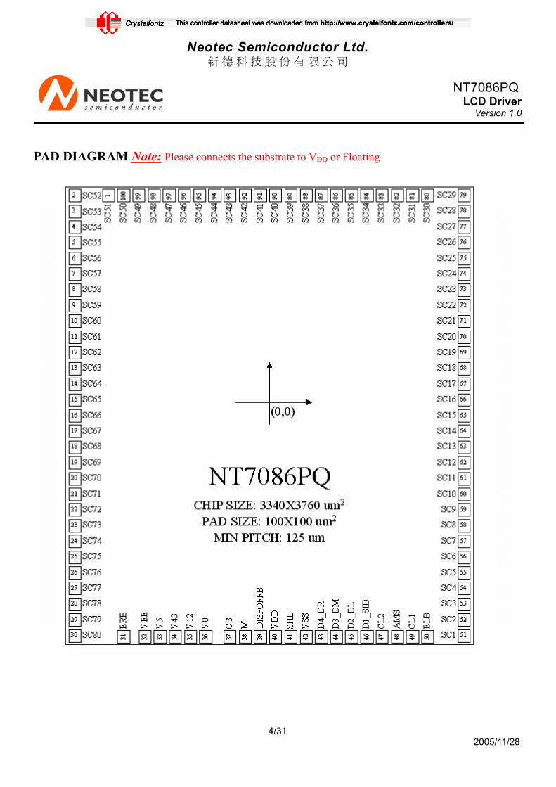
PAD DIAGRAM Note: Please connects the substrate to VDD or Floating
4/31
2005/11/28
This controller datasheet was downloaded from http://www.crystalfontz.com/controllers/Crystalfontz

Neotec Semiconductor Ltd. 新 德 科 技 股 份 有 限 公 司
NT7086PQ
LCD Driver Version 1.0
PAD LOCATION
Pad No. Pad name X Y Pad No. Pad name X Y 1 SC51 -1313.50 1746.00 51 SC1 -1754.00 2 SC52 1746.00 52 SC2 -1629.00 3 SC53 1621.00 53 SC3 -1504.00 4 SC54 1496.00 54 SC4 -1379.00 5 SC55 1371.00 55 SC5 -1254.00 6 SC56 1246.00 56 SC6 -1129.00 7 SC57 1121.00 57 SC7 -1004.00 8 SC58 996.00 58 SC8 -879.00 9 SC59 871.00 59 SC9 -754.00 10 SC60 746.00 60 SC10 -629.00 11 SC61 621.00 61 SC11 -504.00 12 SC62 496.00 62 SC12 -379.00 13 SC63 371.00 63 SC13 -254.00 14 SC64 246.00 64 SC14 -129.00 15 SC65 121.00 65 SC15 -4.00 16 SC66 -4.00 66 SC16 121.00 17 SC67 -129.00 67 SC17 246.00 18 SC68 -254.00 68 SC18 371.00 19 SC69 -379.00 69 SC19 496.00 20 SC70 -504.00 70 SC20 621.00 21 SC71 -629.00 71 SC21 746.00 22 SC72 -754.00 72 SC22 871.00 23 SC73 -879.00 73 SC23 996.00 24 SC74 -1004.00 74 SC24 1121.00 25 SC75 -1129.00 75 SC25 1246.00 26 SC76 -1254.00 76 SC26 1371.00 27 SC77 -1379.00 77 SC27 1496.00 28 SC78 -1504.00 78 SC28 1621.00 29 SC79 -1629.00 79 SC29
1542.00
30 SC80
-1544.00
80 SC30 1311.50 31 ERB -1218.40 81 SC31 1186.50 32 VEE -1048.70 82 SC32 1061.50 33 V5 -923.70 83 SC33 936.50 34 V43 -798.70 84 SC34 811.50 35 V12 -673.70 85 SC35 686.50 36 V0 -548.70 86 SC36 561.50 37 CS -380.00 87 SC37 436.50 38 M -255.00 88 SC38 311.50 39 DISPOFFB -130.00 89 SC39 186.50 40 VDD -5.00 90 SC40 61.50 41 SHL 120.10 91 SC41 -63.50 42 VSS 245.10 92 SC42 -188.50 43 D4_DR 370.10 93 SC43 -313.50 44 D3_DM 495.10 94 SC44 -438.50 45 D2_DL 620.10 95 SC45 -563.50 46 D1_SID 745.10 96 SC46 -688.50 47 CL2 870.10 97 SC47 -813.50 48 AMS 995.10 98 SC48 -938.50 49 CL1 1120.10 99 SC49 -1063.50 50 ELB 1245.10
-1754.00
100 SC50 -1188.50
1746.00
5/31
2005/11/28
This controller datasheet was downloaded from http://www.crystalfontz.com/controllers/Crystalfontz

Neotec Semiconductor Ltd. 新 德 科 技 股 份 有 限 公 司
NT7086PQ
LCD Driver Version 1.0
BLOCK DIAGRAM
80-bit 4-level driver
80-bit level driver
80 bit data latch /common data bidirectional shift register
20 X 4-bits segment databidirectional shift register
Data latch control
Power downfunction
Clockcontrol
Outputlevel
selector
VEE
DISPOFFBM
CL1CL2
CSAMS
ELB
VDDVSS
D1_SID
ERB
/
D2_DLD3_DMD4_DR
SCK
LCK
. . . . . . . . . . . . . .
. . . . . . . . . . . . . .
. . . . . . . . . . . . . .
V0V12V43V5
SC78 SC80SC79SC3SC2SC1. . . . . .
6/31
2005/11/28
This controller datasheet was downloaded from http://www.crystalfontz.com/controllers/Crystalfontz

Neotec Semiconductor Ltd. 新 德 科 技 股 份 有 限 公 司
NT7086PQ
LCD Driver Version 1.0
BLOCK DESCRIPTION
NAME FUNCTION COM / SEG
Clock control
Generates latch clock (LCK), shift clock (SCK) and control clock timing according to the input of CL1, CL2 and control inputs (CS, AMS). In common driver application mode, this block generates the shift clock (LCK) for the common data Bi-directional shift register.
COM / SEG
Data latch control
Determines the direction of segment data shift, and input data of each Data latch Bi-directional shift register. In 4-bit segment data parallel transfer mode, data is shifted by a 4-bit unit. In common driver application mode, data is transferred to the common data shift register directly, which disables this block.
SEG
Power down function
Controls the clock enable state of the current driver according to the input value of enable pin (ELB or ERB). If enable input value is “Low”, every clock of the current driver is enabled and the clock control block works. But if enable input is “High”, current driver is disabled and the input data value has no effect on the output level. So power consumption can be lowered.
SEG
Output level selector
Controls the output voltage level according to the input control pin (M and DISPOFFB) (refer to PIN DESCRIPTION). COM / SEG
20x4-bitsegment data
bi-directional shift register
Stores output data value by shifting the input values. In 1-bit serial interface mode application, all 80 shift clocks (SCK) are needed to store all the display data. But in 4-bit parallel transfer mode application, only 20 clocks are needed. In common driver application mode, this block does not work.
SEG
80-bit data latch /
common data bi-directional shift register
In segment driver application mode, the data from the 20x4-bit segment data shift register are latched for segment driver output. In single-type common driver application, 1-bit input data (from DL or DR pin) is shifted and latched by the direction according to the SHL signal input. In dual-type common application mode, 80-bit registers are divided by two blocks and controlled Independently (refer to NOTE 3).
COM / SEG
80-bit level shifter
Voltage level shifter block for high voltage part. The inputs of this block are of logical voltage level and the outputs of this block are at high voltage level value. These values are input in to the driver.
SEG
80-bit 4-level driver
Selects the output voltage level according to M and latched data value. If the data value is "High" the driver output is at selected voltage level (V0 or V5), and in the reverse case the driver output value is at the non-selected level (V12 or V43). In segment driver application mode, non-selected output value is V2 or V3 and when in common driver application, this value becomes V1 or V4.
SEG
7/31
2005/11/28
This controller datasheet was downloaded from http://www.crystalfontz.com/controllers/Crystalfontz

Neotec Semiconductor Ltd. 新 德 科 技 股 份 有 限 公 司
NT7086PQ
LCD Driver Version 1.0
PIN DESCRIPTION
PIN I/O NAME FUNCTION INTERFACE
VDD Logical "High" input port (+5V±10%, +3V± 10%)
VSS 0V (GND) VEE
Power supply
Logical "Low" for high voltage part
Power
V0,V12, V43,V5 I
LCD driver output voltage level
Bias supply voltage input to drive the LCD. Bias voltage divided by the resistance is usually used as a supply voltage source (refer to NOTE 2).
Power
SC1~SC80 O LCD driver output
Display data output pin which corresponds to the respective latch contents. One of V0, V12, V34 and V5 is selected as a display driving voltage source according to the combination of the latched data level and M signal (refer to NOTE 1).
LCD
CL2 I Data shift clock
Clock pulse input for the bi-directional shift register.
– In segment driver application mode, the data is shifted to 20 x4-bit segment data shift. The clock pulse, which was input when the enable bit (ELB/ERB) is in not active condition, is invalid.
– In common driver application mode, the data is shifted to 80-bit common data bi-directional shift register by the CL1 clock. Hence, this clock pin is not used (Open or connect this pin to VDD).
Controller
M I
AC signal for LCD
driver output
Alternate signal input pin for LCD driving. Normal frame inversion signal is input in to this pin.
Controller
CL1 I Data latch clock
– In segment driver application mode, this signal is used for latching the shift register contents at the falling edge of this clock pulse. CL1 pulse "High" level initializes power-down function block.
– In common driver application mode, CL1 is used as a shifting clock of common output data.
Controller
8/31
2005/11/28
This controller datasheet was downloaded from http://www.crystalfontz.com/controllers/Crystalfontz

Neotec Semiconductor Ltd. 新 德 科 技 股 份 有 限 公 司
NT7086PQ
LCD Driver Version 1.0
PIN DESCRIPTION (CONTINUED)
PIN I/O NAME FUNCTION INTERFACE
DISPOFFB I Display OFF control
Control input pin to fix the driver output (SC1~SC80) to V0 level, during "Low" value input. LCD becomes non-selected by V0 level output from every output of segment drivers and every output of common drivers.
Controller
CS I COM / SEG
mode control
When CS = "Low", NT7086PQ is used as an 80-bit segment driver. When CS = "High", NT7086PQ is set to an 80-bit common driver
VDD/VSS
According to the input value of the AMS and the CS pin, application mode of NT7086PQ is differs as shown below.
CS AMS Application mode COM/SEG
0 0 4-bit parallel interface mode
0 1 1-bit serial interface mode
SEG
1 0 Single type application Mode
1 1 Dual type application mode
COM
AMS I Application mode select
VDD/VSS
D1_SID, D2_DL, D3_DM, D4_DR
I/O
Display data input/ serial input data/ left , right data input
output
-In segment driver mode, these pins are used as 4-bit data input pin (when 4-bit parallel interface mode AMS= ”low”), or D1_SID is used as serial data input pin and other pins are not used (connect these to VDD) (when 1-bit serial interface mode AMS= ”high”).
-In common driver mode, the data is shifted from D2_DL (D4_DR) to D4_DR (D2_DL), when in single interface mode (AMS= ”Low”). In dual-type application case, the data are shifted from D2_DL and D3_DM (D4_DR and D3_DM) to D4_DR(D2_DL). In each case the direction of the data shift and the connection of data pins are determined by SHL input (refer to NOTE 3, NOT 4).
Controller
9/31
2005/11/28
This controller datasheet was downloaded from http://www.crystalfontz.com/controllers/Crystalfontz

Neotec Semiconductor Ltd. 新 德 科 技 股 份 有 限 公 司
NT7086PQ
LCD Driver Version 1.0
PIN DESCRIPTION (CONTINUED)
PIN I/O NAME FUNCTION INTERFACE
SHL I Shift
direction control
When SHL = "Low", data is shifted from left to right. When SHL = "High", the direction is reversed. (refer to NOTE3)
-In segment driver mode, the internal operation is enabled only when enable input (ELB or ERB) is "Low" (power down function). When several drivers a serially connected, the enable state of each driver is shifted according to the SHL input. Connect these pins as below.
Segment driver SHL ELB ERB L Output (open) Input (VSS) H Input (VSS) Output(open)
ELB, ERB I/O Enable data
input/ output
-In common driver mode, the power down
function is not used. Open these pins.
VDD/VSS
NOTE 1. Output level control "X": don't care
Output level (CS1~CS80) M Latched data DISPOFFB SEG Mode COM Mode L L H V12(V2) V12(V1) L H H V0 V5 H L H V43(V3) V43(V4) H H H V5 V0 X X L V0 V0
10/31
2005/11/28
This controller datasheet was downloaded from http://www.crystalfontz.com/controllers/Crystalfontz

Neotec Semiconductor Ltd. 新 德 科 技 股 份 有 限 公 司
NT7086PQ
LCD Driver Version 1.0
NOTE 2. LCD Driving Voltage Application Circuit (1) Segment driver application (CS = “Low”)
(2) Common driver application (CS = “High”)
11/31
2005/11/28
This controller datasheet was downloaded from http://www.crystalfontz.com/controllers/Crystalfontz

Neotec Semiconductor Ltd. 新 德 科 技 股 份 有 限 公 司
NT7086PQ
LCD Driver Version 1.0
NOTE 3. Data Shift Direction according to Control Signals (1) When CS = “Low” (segment driver application)
AMS SHL Application mode Data Direction Input pin
L
D1D2D3D4
D1
D2
D3
D4
SC1
SC2
SC3
SC4
D1
D2
D3
D4
SC73
SC74
SC75
SC76
D1
D2
D3
D4
SC77
SC78
SC79
SC80. . . . . . . .
. . . . . . . .
Shift direction
Last data Frist data
L
H
4-bit parallel data transfer mode (SEG)
Frist data
Shift direction
SC1
SC2
SC3
SC4
D4
D3
D2
D1
SC73
SC74
SC75
SC76
D4
D3
D2
D1
SC77
SC78
SC79
SC80. . . . . . . .
. . . . . . . .
D1D2D3D4
Last data
D1
D2
D3
D4
D1_SID, D2_DL, D3_DM, D4_DR
L
SC1
SC2
SC3
SC4
SC73
SC74
SC75
SC76
SC77
SC78
SC79
SC80
. . . . . . . .
Shift direction
Last data (D1_SID) Frist data H
H
1-bit serial data transfer mode (SEG) S
C1
SC2
SC3
SC4
SC73
SC74
SC75
SC76
SC77
SC78
SC79
SC80
. . . . . . . .
Shift direction
Frist data Last data
D1_SID
12/31
2005/11/28
This controller datasheet was downloaded from http://www.crystalfontz.com/controllers/Crystalfontz

Neotec Semiconductor Ltd. 新 德 科 技 股 份 有 限 公 司
NT7086PQ
LCD Driver Version 1.0
(2) When CS = “High” (common driver application)
AMS SHL Application mode Data Direction Input pin
L
SC78
SC79
SC80
. . . . .
Shift direction
SC1
SC2
SC3
. . . . .
Input data(D2_DL)
Output data(D4_DR)
. . . . .SC38
SC39
SC40
SC41
SC42
SC43 . . . . .
D2_DL
L
H
Single-type Application mode (COM) S
C78
SC79
SC80
. . . . .
Shift direction
SC1
SC2
SC3
. . . . .
Output data(D2_DL)
Input data(D4_DR)
. . . . .SC38
SC39
SC40
SC41
SC42
SC43 . . . . .
D4_DR
L
SC78
SC79
SC80
. . . . .SC1
SC2
SC3
. . . . .
Input data 1(D2_DL)
Output data(D4_DR)
. . . . .SC38
SC39
SC40
SC41
SC42
SC43 . . . . .
Shift direction
Input data 2(D3_DM)
D2_DL, D3_DM
H
H
Dual-type Application mode (COM)
SC78
SC79
SC80
. . . . .SC1
SC2
SC3
. . . . .
Output data(D2_DL)
Input data 1(D4_DR)
. . . . .SC38
SC39
SC40
SC41
SC42
SC43 . . . . .
Shift direction
Input data 2(D3_DM)
D4_DR, D3_DM
13/31
2005/11/28
This controller datasheet was downloaded from http://www.crystalfontz.com/controllers/Crystalfontz
Neotec Semiconductor Ltd. 新 德 科 技 股 份 有 限 公 司
NT7086PQ
LCD Driver Version 1.0
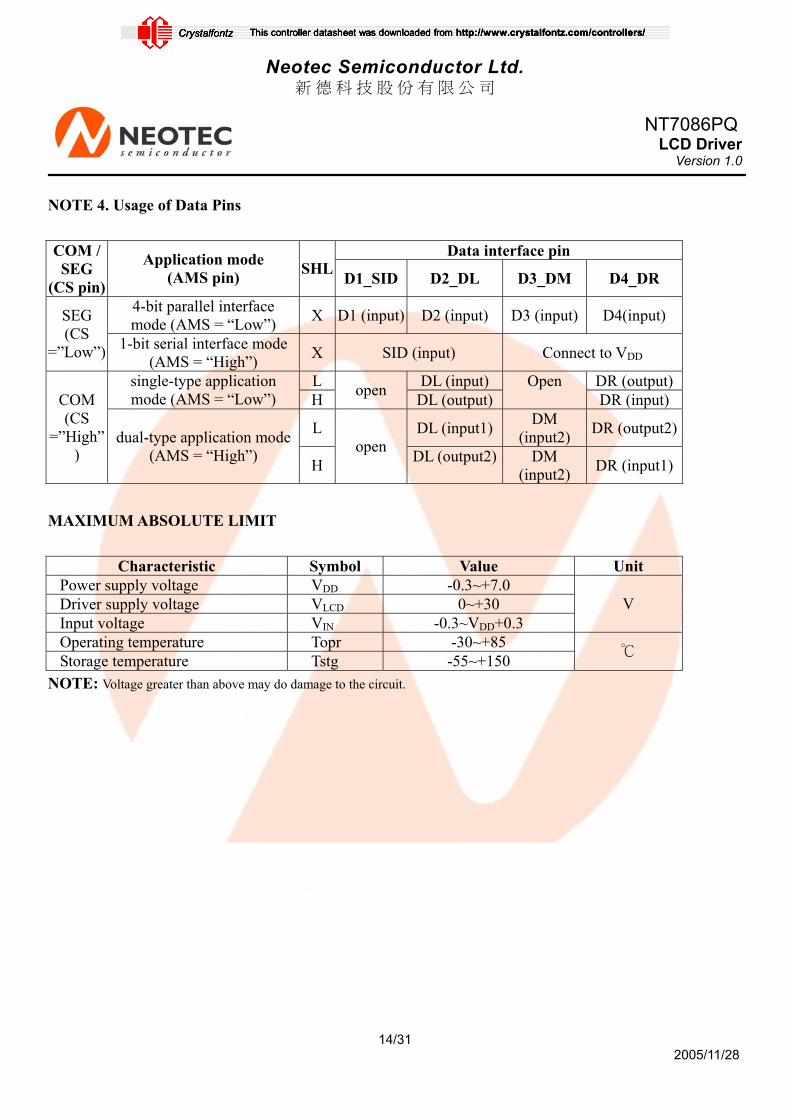
NOTE 4. Usage of Data Pins
Data interface pin COM / SEG
(CS pin)
Application mode (AMS pin) SHL D1_SID D2_DL D3_DM D4_DR
4-bit parallel interface mode (AMS = “Low”) X D1 (input) D2 (input) D3 (input) D4(input) SEG
(CS =”Low”) 1-bit serial interface mode
(AMS = “High”) X SID (input) Connect to VDD
L DL (input) DR (output)single-type application mode (AMS = “Low”) H open DL (output)
Open DR (input)
L DL (input1) DM (input2) DR (output2)
COM (CS
=”High”)
dual-type application mode (AMS = “High”) H
open DL (output2)
DM (input2) DR (input1)
MAXIMUM ABSOLUTE LIMIT
Characteristic Symbol Value Unit Power supply voltage VDD -0.3~+7.0 Driver supply voltage VLCD 0~+30 Input voltage VIN -0.3~VDD+0.3
V
Operating temperature Topr -30~+85 Storage temperature Tstg -55~+150
℃
NOTE: Voltage greater than above may do damage to the circuit.
14/31
2005/11/28
This controller datasheet was downloaded from http://www.crystalfontz.com/controllers/Crystalfontz

Neotec Semiconductor Ltd. 新 德 科 技 股 份 有 限 公 司
NT7086PQ
LCD Driver Version 1.0
ELECTRICAL CHARACTERISTICS DC CHARACTERISTICS (1) Segment Driver Application
(VSS = 0V, Ta = - 30 ~ +85°C) Characteristic Symbol Test Condition Min. Typ. Max. Unit
VDD - 2.7 - 5.5 Operating Voltage 1 VLCD VIN=VDD-VEE 6 - 28
VIH - 0.8VDD - VDD Input voltage (1) VIL - 0 - 0.2VDD
V
VOH ICH=-0.4mA VDD-0.4 - - Input voltage (2) VOL IOH=-0.4mA - - 0.4 V
Input leakage current 1 (1) IIL1 VIN=VDD to VSS -10 - 10
Input leakage current 2 (3) IIL2 VIN=VDD to VEE -25 - 25
μA
On resistance(4) RON ION=100μA - 2 4 kΩ
ISTBY fCL1=32kHZ, M=VSS VSS PIN - - 100 μAVDD=5V - - 5 IDD VDD=3V - - 2 mASupply
current(5) IEE
fCL1=32kHZ FM=80HZVDD=5V - - 500 μA
NOTES: 1. Applied to CL1, CL2, ELB, ERB, D1_SID - D4_DR, SHL, DISPOFFB, M, CS, AMS pin 2. ELB, ERB pin 3. V0, V12, V43, V5 pin 4. VLCD = VDD - VEE, V0 = VDD = 5V, V5= VEE = -23 V V12 = VDD-2/n(VLCD), V43 = VEE+2/n(VLCD), n = 17 (1/256 duty, 1/17 bias) 5. V0 = VDD, V12 = 1.71V(VDD = 5V) or -0.06V (VDD = 3V), V43 = -19.71 V(VDD = 5V) or -19.94V (VDD = 3V), V5 = VEE = -23V, no-load condition (1/256 duty, 1/17 bias) 4-bit parallel interface mode ISTBY : VDD = 5V, fCL2 = 5.12MHz, SHL = VSS, DISPOFFB = VDD, M = VSS, display data pattern = 0000 IDD : VDD = 3V, fCL2 = 4MHz, display data pattern = 0101 VDD = 5 V, fCL2 = 5.12MHz, display data pattern = 0101 IEE : VDD = 5V, fCL2 = 5.12MHz, display data pattern = 0101, VEE pin
15/31
2005/11/28
This controller datasheet was downloaded from http://www.crystalfontz.com/controllers/Crystalfontz

Neotec Semiconductor Ltd. 新 德 科 技 股 份 有 限 公 司
NT7086PQ
LCD Driver Version 1.0
DC CHARACTERISTICS (CONTINUED) (2) Common Driver Application
(VSS = 0V, Ta = - 30 ~ +85°C) Characteristic Symbol Test Condition Min. Typ. Max. Unit
VDD - 2.7 - 5.5 Operating Voltage 1 VLCD VIN=VDD-VEE 6 - 28
VIH - 0.8VDD - VDD Input voltage (1) VIL - 0 - 0.2VDD
V
VOH ICH=-0.4mA VDD-0.4 - - Input voltage (3) VOL IOH=-0.4mA - - 0.4 V
Input leakage current 1 (1) IIL1 VIN=VDD to VSS -10 - 10
Input leakage current 2 (2) IIL2 VIN=0V, VDD=5V(Pull up) -50 -125 -250
μA
Input leakage current 3 (4) IIL3 VIN=VDD to VEE -25 - 25
On resistance(5) RON ION=100μA - 2 4 kΩ
ISTBY fCL1=32kHZ, M=VSS VSS PIN - - 100 VDD=5V - - 200 IDD VDD=3V - - 120
Supply current(6)
IEE fCL1=32kHZ FM=80HZ
VDD=5V - - 150
μA
NOTES: 1. Applied to CL1, D2_DL (SHL = LOW), D4_DR (SHL = HIGH), SHL, DISPOFFB, M, CS, AMS pin 2. Pull-up input pins : CL2, D1_SID, D3_DM (AMS = HIGH), ELB (SHL = LOW), ERB (SHL = HIGH) 3. D2_DL (SHL = HIGH) , D4_DR (SHL = LOW) pin 4. V0, V12, V43, V5 pin 5. VLCD = VDD-VEE, V0 = VDD = 5V, V5 = VEE = -23V V12 = VDD-1/n(VLCD), V43 = VEE+1/n(VLCD), n = 17(1/256 duty, 1/17 bias) 6. V0 = VDD, V12 = 3.35V (VDD = 5V) or 1.47V (VDD = 3V), V43 = -21.35V (VDD = 5 V) or -21.47V (VDD = 3 V), V5 = VEE = -23 V, no-load condition (1/256 duty, 1/17 bias) single-type mode operation : AMS = VSS, SHL = VSS, DISPOFFB = VDD D1_SID = D3_DM = VDD, D4_DR = OPEN, ELB = ERB = OPEN, ISTBY : VDD = 5V, M = VSS, D2_DL = VSS IDD : fM = 80Hz, D2_DL = VDD VDD = 3 V, display data pattern = 10000000..., 01000000..., 00100000..., 00010000..., .. VDD = 5 V, display data pattern = 10000000..., 01000000..., 00100000..., 00010000..., .. IEE : fM = 80Hz, D2_DL = VDD VDD = 5V, current through VEE Pin, display data pattern = 10000000..., 01000000..., 00100000..., 00010000...
16/31
2005/11/28
This controller datasheet was downloaded from http://www.crystalfontz.com/controllers/Crystalfontz

Neotec Semiconductor Ltd. 新 德 科 技 股 份 有 限 公 司
NT7086PQ
LCD Driver Version 1.0
AC CHARACTERISTICS (1) Segment Driver Application
(VSS = 0V, Ta = - 30 ~ +85°C) (1) VDD=5V±10% (2) VDD=3V±10% Characteristic Symbol Test condition Min. Typ. Max. Min. Typ. Max. Unit
Clock cycle time tCY Duty=50% 125 - - 250 - - Clock pulse width tWCK - 45 - - 95 - - Clock rise/ fall time tR / tF - - - - - - 30 Data set-up time tDS - 30 - 65 - - Data hold time tDH - 30 - 65 - - Clock set-up time tCS - 80 - 120 - - Clock hold time tCH - 80 - 120 - -
ELB output 60 125 Propagation delay time tPHL ERB output - - 60 - - 125 ELB input 30 65 ELB,ERB set-up time tPSU ERB input 30 - - 65 - -
ns
DISPOFFB low pulse width tWDL - 1.2 - - 1.2 - - μs
DISPOFFB clear time tCD - 100 - - 100 - - ns M – OUT propagation delay time tPD1 - - 1.0 - - 1.2
CL1 – OUT propagation delay time tPD2 - - 1.0 - - 1.2
DISPOFFB – OUT propagation delay time tPD3
CL=15pF
- - 1.0 - - -
μs
(2) Common Driver Application
(VSS = 0V, Ta = - 30 ~ +85°C) (1) VDD=5V±10% (2) VDD=3V±10% Characteristic Symbol Test condition Min. Typ. Max. Min. Typ. Max. Unit
Clock cycle time tCY Duty=50% 250 - - 500 - - Clock pulse width tWCK - 45 - - 95 - - Clock rise/ fall time tR / tF - - - 50 - - 50 Data set-up time tDS - 30 - 65 - - Data hold time TDH - 30 - 65 - -
ns
DISPOFFB low pulse width tWDL - 1.2 - - 1.2 - - μs
DISPOFFB clear time tCD - 100 - - 100 - - Output delay time tDL - - 200 - - 250 ns
M – OUT propagation delay time tPD1 - - 1.0 - - 1.2
CL1 – OUT propagation delay time tPD2 - - 1.0 - - 1.2
DISPOFFB – OUT propagation delay time tPD3
CL=15pF
- - 1.0 - - 1.2
μs
17/31
2005/11/28
This controller datasheet was downloaded from http://www.crystalfontz.com/controllers/Crystalfontz

tWCK
CL2
0.8VDD
0.2VDD0.8VDD
0.2VDD
0.2VDD
0.2VDD0.8VDD
0.2VDD0.8VDD 0.8VDD
tWCK
tR tFtCY
tCS
tWCK
tCH
D1_SID - D4_DR
DISPOFFB
0.2VDD0.8VDD
tDS tDH
tCDtWDL
CL1
CL1
CL2
ELB, ERB(Output 1)
1 2 3 19 200.8VDD
0.2VDD
M
tPHL
ELB, ERB(Input 2)
0.2VDD
0.2VDDtPSU
CL1
DISPOFFB
SC1 - SC80(Latched data)
0.2VDD
0.8VDD0.2VDD
0.8VDD0.2VDD
tPD1tPD2
tPD3
Neotec Semiconductor Ltd. 新 德 科 技 股 份 有 限 公 司
NT7086PQ
LCD Driver Version 1.0
18/31
2005/11/28
(3) Segment Driver Application Timing
This controller datasheet was downloaded from http://www.crystalfontz.com/controllers/Crystalfontz

(*1) When in single-type interface mode DI=>DDL(SHL=L), D4_DR(SHL=H) DO=>D4_DR(SHL=L), D2_DL(SHL=H) When in dual-type interface mode DI=>D2_DL and D3_DM(SHL=L),D4_DR and D3_DM(SHL=H) DO=>D4_DR(SHL=L), D2_DL(SHL=H)
CL1 tDWCKH
tR tF
0.8VDD
0.2VDDtF
tCY
0.8VDD
0.2VDD
0.8VDD0.2VDD
tDS tDH
0.8VDD0.2VDD
tDL
(*1) DI
tWDLtCD
DISPOFFB
(*1) DO 0.8VDD0.2VDD
CL1 0.2VDD
0.8VDD0.2VDDM
DISPOFFB 0.8VDD0.2VDD
SC1 - SC80(Latched data)
tPD1tPD2
tPD3
Neotec Semiconductor Ltd. 新 德 科 技 股 份 有 限 公 司
NT7086PQ
LCD Driver Version 1.0
19/31
2005/11/28
(4) Common Driver Application Timing
This controller datasheet was downloaded from http://www.crystalfontz.com/controllers/Crystalfontz
Neotec Semiconductor Ltd. 新 德 科 技 股 份 有 限 公 司
NT7086PQ
LCD Driver Version 1.0
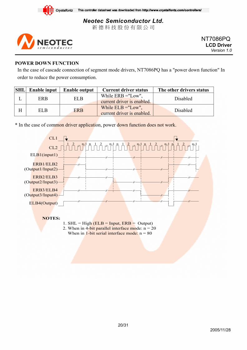
POWER DOWN FUNCTION In the case of cascade connection of segment mode drivers, NT7086PQ has a "power down function" In order to reduce the power consumption.
SHL Enable input Enable output Current driver status The other drivers status
L ERB ELB While ERB ="Low", current driver is enabled. Disabled
H ELB ERB While ELB ="Low", current driver is enabled. Disabled
* In the case of common driver application, power down function does not work.
CL11 2 n-1 n 1 2 n-1 n 1 2 n-1 n 1 2 n-1 n 1 2 n-1
CL2
ELB1(input1)
ERB1/ELB2(Output1/Input2)
ERB2/ELB3(Output2/Input3)
ERB3/ELB4(Output3/Input4)
ELB4(Output)
NOTES:1. SHL = High (ELB = Input, ERB = Output)2. When in 4-bit parallel interface mode: n = 20 When in 1-bit serial interface mode: n = 80
20/31
2005/11/28
This controller datasheet was downloaded from http://www.crystalfontz.com/controllers/Crystalfontz

Neotec Semiconductor Ltd. 新 德 科 技 股 份 有 限 公 司
NT7086PQ
LCD Driver Version 1.0
21/31
2005/11/28
OPERATION TIMING DIAGRAM (1) 4-bit parallel mode interface segment driver When SHL= ”Low”
CL219 20 1 2 3 19 20 1 2
D1_SID SC5 SC1 SC77 SC73 SC5 SC1 SC77 SC73
D2_DL SC6 SC2 SC78 SC74 SC6 SC2 SC78 SC74
D3_DM SC7 SC3 SC79 SC75 SC7 SC3 SC79 SC75
D4_DR SC8 SC4 SC80 SC76 SC8 SC4 SC80 SC76
SC69
SC70
SC71
SC72ERB(Input)
ELB(Onput)CL1
SC1 - SC80
When SHL= ”High”
CL219 20 1 2 3 19 20 1 2
D1_SID SC76 SC80 SC4 SC8 SC76 SC80 SC4 SC8
D2_DL SC75 SC79 SC3 SC7 SC75 SC79 SC3 SC7
D3_DM SC74 SC78 SC2 SC6 SC74 SC78 SC2 SC6
D4_DR SC73 SC77 SC1 SC5 SC73 SC77 SC1 SC5
SC12
SC11
SC10
SC9ELB(Input)
ERB(Onput)CL1
SC1 - SC80
This controller datasheet was downloaded from http://www.crystalfontz.com/controllers/Crystalfontz

CL279 80 1 2 3 79 80 1 2
D1_SID SC2 SC1 SC80 SC79 SC2 SC1 SC80 SC79SC78
ERB(Input)
ELB(Onput)CL1
SC1 - SC80
Neotec Semiconductor Ltd. 新 德 科 技 股 份 有 限 公 司
NT7086PQ
LCD Driver Version 1.0
22/31
2005/11/28
(2) 1-bit serial mode interface segment driver When SHL= ”Low”
When SHL= “High”
CL279 80 1 2 3 79 80 1 2
D1_SID SC79 SC80 SC1 SC2 SC79 SC80 SC1 SC2SC3
ELB(Input)
ERB(Onput)CL1
SC1 - SC80
This controller datasheet was downloaded from http://www.crystalfontz.com/controllers/Crystalfontz

79 80 1 2 79 80 1 2CL1
D2_DL
D4_DR
COM_DATA1
COM_DATA3
COM_DATA2
COM_DATA79
COM_DATA80
Current Driver's COMMON area
Neotec Semiconductor Ltd. 新 德 科 技 股 份 有 限 公 司
NT7086PQ
LCD Driver Version 1.0
23/31
2005/11/28
(3) Single type interface mode common driver When SHL= “Low”
When SHL= ”High”
79 80 1 2 79 80 1 2CL1
D4_DR
D2_DL
COM_DATA1
COM_DATA3
COM_DATA2
COM_DATA79
COM_DATA80
Current Driver's COMMON area
This controller datasheet was downloaded from http://www.crystalfontz.com/controllers/Crystalfontz

1 2 3 39 40 1 2 3 39 40CL1
D2_DL
D3_DM
D4_DR
COM_DATA1
COM_DATA2
COM_DATA3
COM_DATA39
COM_DATA40
COM_DATA41
COM_DATA42
COM_DATA43
COM_DATA79
COM_DATA80
Neotec Semiconductor Ltd. 新 德 科 技 股 份 有 限 公 司
NT7086PQ
LCD Driver Version 1.0
24/31
2005/11/28
(4) Dual-type interface mode common driver When SHL= “Low”
When SHL= “High”
1 2 3 39 40 1 2 3 39 40CL1
D2_DL
D3_DM
D4_DR
COM_DATA1
COM_DATA2
COM_DATA3
COM_DATA39
COM_DATA40
COM_DATA41
COM_DATA42
COM_DATA43
COM_DATA79
COM_DATA80
This controller datasheet was downloaded from http://www.crystalfontz.com/controllers/Crystalfontz

199 200 1 200 1 199 200 1 199 200CL1
M
Latched data (SEG)
COM1
COM_DATA1
COM_DATA200
COM_DATA199
SEG_DATA1
COM199
V0V1
V4V5
V0V1
V4V5
COM200V0V1
V4V5
SEG1V0V1
V4V5
CL2
V2V3
CL1
1 2 18 19 20 1
D1 - D4
Latched data
M
Enable Out
Neotec Semiconductor Ltd. 新 德 科 技 股 份 有 限 公 司
NT7086PQ
LCD Driver Version 1.0
25/31
2005/11/28
(5) Common / Segment driver timing (1/200 duty)
This controller datasheet was downloaded from http://www.crystalfontz.com/controllers/Crystalfontz

Neotec Semiconductor Ltd. 新 德 科 技 股 份 有 限 公 司
NT7086PQ
LCD Driver Version 1.0
26/31
2005/11/28
APPLICATION INFORMATION 1-bit serial interface mode (80 Ch. Segment mode) a) Lower view (SHL= L, AMS= H)
b) Upper view (SHL= H, AMS= H)
This controller datasheet was downloaded from http://www.crystalfontz.com/controllers/Crystalfontz

Neotec Semiconductor Ltd. 新 德 科 技 股 份 有 限 公 司
NT7086PQ
LCD Driver Version 1.0
27/31
2005/11/28
4-bit parallel interface mode (80 Ch. Segment driver) a) Lower view (SHL= L, AMS = L)
b) Upper view (SHL= H, AMS = L)
This controller datasheet was downloaded from http://www.crystalfontz.com/controllers/Crystalfontz
Neotec Semiconductor Ltd. 新 德 科 技 股 份 有 限 公 司
NT7086PQ
LCD Driver Version 1.0
28/31
2005/11/28
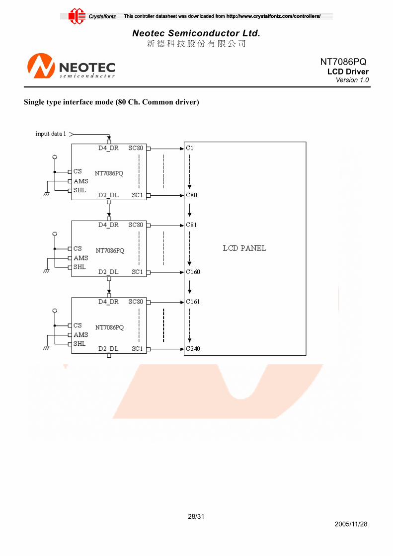
Single type interface mode (80 Ch. Common driver)
This controller datasheet was downloaded from http://www.crystalfontz.com/controllers/Crystalfontz

Neotec Semiconductor Ltd. 新 德 科 技 股 份 有 限 公 司
NT7086PQ
LCD Driver Version 1.0
29/31
2005/11/28
Dual-type interface mode (40 Ch. + 40Ch. Common driver)
NOTE: Using this application mode (dual-type common mode), the duty ratio can be reduced to half. In case, 1/200 duty can be used to driver the 400 common LCD panel.
This controller datasheet was downloaded from http://www.crystalfontz.com/controllers/Crystalfontz

Neotec Semiconductor Ltd. 新 德 科 技 股 份 有 限 公 司
NT7086PQ
LCD Driver Version 1.0
30/31
2005/11/28
APPLICATION CIRCUIT EXAMPLE
This controller datasheet was downloaded from http://www.crystalfontz.com/controllers/Crystalfontz

VDD
/DISPOFF
VEE
VDD
VSS
VDD
VSS
VSS
VEE
Neotec Semiconductor Ltd. 新 德 科 技 股 份 有 限 公 司
NT7086PQ
LCD Driver Version 1.0
31/31
2005/11/28
PRECAUTIONS Precautions when connecting or disconnecting the power supply
This IC has a high-voltage LCD driver, so it may be permanently damaged by a high current which may flow if voltage is supplied to the LCD drive power supply while the logic system power supply is floating. The details are as follows.
When connecting the power supply, connect the LCD drive power after connecting the logic system power. Furthermore, when disconnecting the power, disconnect the logic system power after disconnecting the LCD drive power.
And when connecting the logic power supply, the logic condition of this IC inside is insecure. Therefore connect the LCD drive power supply after resetting logic condition of this IC inside on /DISPOFF function. After that, cancel the /DISPOFF function after the LCD drive power supply has become stable. Furthermore, when disconnecting the power, set the LCD drive output pins to level V5 on /DISPOFF function. Then, disconnect the logic system power after disconnecting the LCD drive power.
When connecting the power supply, follow the recommended sequence shown here.
This controller datasheet was downloaded from http://www.crystalfontz.com/controllers/Crystalfontz

This controller datasheet was downloaded from http://www.crystalfontz.com/controllers/Crystalfontz