new experiment for understanding the physical mechanisms
TRANSCRIPT
HAL Id: tel-01281828https://tel.archives-ouvertes.fr/tel-01281828v2
Submitted on 18 Apr 2016
HAL is a multi-disciplinary open accessarchive for the deposit and dissemination of sci-entific research documents, whether they are pub-lished or not. The documents may come fromteaching and research institutions in France orabroad, or from public or private research centers.
L’archive ouverte pluridisciplinaire HAL, estdestinée au dépôt et à la diffusion de documentsscientifiques de niveau recherche, publiés ou non,émanant des établissements d’enseignement et derecherche français ou étrangers, des laboratoirespublics ou privés.
New experiment for understanding the physicalmechanisms of ultrafast laser-induced electron emission
from novel metallic nanotipsMina Bionta
To cite this version:Mina Bionta. New experiment for understanding the physical mechanisms of ultrafast laser-inducedelectron emission from novel metallic nanotips. Physics [physics]. Université Paul Sabatier - ToulouseIII, 2015. English. �NNT : 2015TOU30220�. �tel-01281828v2�
THÈSEEn vue de l’obtention du
DOCTORAT DE L’UNIVERSITÉ DE TOULOUSEDélivré par l’Université Toulouse III – Paul Sabatier
Discipline ou spécialité: Physique
New experiment for understanding the physicalmechanisms of ultrafast laser-induced electron emission
from novel metallic nanotips
Présentée et soutenue parMina R. BIONTA
15 September 2015
JURY
Mme Béatrice CHATEL Directrice de recherche, CNRS, LCAR, Toulouse Directrice de ThèseM. Benoît CHALOPIN Maître de conferences, LCAR, Université Paul Sabatier Toulouse III Co-directeur de ThèseM.me Natalia DEL FATTI Professeur, Université Lyon I, ILM, Lyon RapporteurM. Eric CONSTANT Directeur de recherche, CNRS, CELIA, Bordeaux RapporteurM. Jesse GROENEN Professeur, CEMES, Université Paul Sabatier Toulouse III Président du JuryM. Hamed MERDJI Chercheur, CEA, IRAMIS - LIDYL, Saclay Examiner
École doctorale: Sciences de la Matière (SDM)Unité de recherche: Laboratoire Collisions Agrégats Réactivité (LCAR IRSAMC UMR5589)
Directrice de Thèse: Béatrice CHATELCo-directeur de Thèse: Benoît CHALOPIN


Ph.D. Thesis
New experiment for understanding the physicalmechanisms of ultrafast laser-induced electron emission
from novel metallic nanotips
presented by:Mina R. BIONTA
A thesis submitted to theGraduate School Sciences de la Matière (SDM) of the
Université Toulouse III – Paul Sabatierin partial fulfillment of the requirements for the degree of
Doctor of Philosophy (Ph.D.) of the Université de Toulouse
Toulouse, France. 15 September 2015
JURY
Mme Béatrice CHATEL Directrice de recherche, CNRS, LCAR, Toulouse AdvisorM. Benoît CHALOPIN Maître de conferences, Université Paul Sabatier Toulouse III, LCAR, Toulouse Co-advisorM.me Natalia DEL FATTI Professeur, Université Lyon I, ILM, Lyon ReviewerM. Eric CONSTANT Directeur de recherche, CNRS, CELIA, Bordeaux ReviewerM. Jesse GROENEN Professeur, Université Paul Sabatier Toulouse III, CEMES, Toulouse Jury PresidentM Hamed MERDJI Chercheur, CEA, IRAMIS - LIDYL, Saclay Examiner
Graduate School: Sciences de la Matière (SDM)Research laboratory: Laboratoire Collisions Agrégats Réactivité (LCAR IRSAMC UMR5589)
Supervisor: Béatrice CHATELCo-supervisor: Benoît CHALOPIN

c© 2015 by Mina R. BIONTANew experiment for understanding the physical mechanisms of ultrafast laser-induced elec-tron emission from novel metallic nanotips
Ph.D. thesis, 15 September 2015
Supervisor: Béatrice CHATEL
Co-Supervisor: Benoît CHALOPIN
Reviewers: Natalia DEL FATTI and Eric CONSTANT
Examiners: Jesse GROENEN and Hamed MERDJI
Université Toulouse III – Paul SabatierSciences de la Matière (SDM)
Laboratoire Collisions Agrégats Réactivité (LCAR IRSAMC UMR5589)
118 Rue de Narbonne – 31062 Toulouse – France


To my parents


Stories are light. Light is precious ina world so dark. Begin at thebeginning. Tell Gregory a story.Make some light.
– Kate DiCamillo,
The Tale of Despereaux


Acknowledgments
First and foremost I would like to thank my advisors Béatrice and Benoît. Their continual
guidance has been amazing and could not be better. This includes not only in terms of scientific
help and direction, but also with helping me with my cross-continental + trans-Atlantic move
and dealing with all the little (and big!) nuances that are the difference between French and
American culture and administration. By the end I was thinking of you as my surrogate French
parents.
I’d also like to thank the rest of our group: Elsa, Stéphane, Laurent, Julien and Sébastien. With-
out you certainly our experiments would not have been able to run so smoothly and I wouldn’t
have been able to get such great data. I’d especially like to thank Sébastien. Thanks for doing
a post-doc in England and coming to LCLS for a beam time. Without you I’d never have found
such a great Ph.D. and would probably still be looking for the perfect project.
I’d also like to thank our collaboration with CEMES, especially Aurélien for teaching me how
to make tips and answering my many questions about materials, and everyone else in the group
with whom I interacted with a lot: Florent, Ludvig, Robin. And of course there was our other
collaboration with GPM in Rouen: Ivan, Jonathan, Angela, Bernard. A great thanks for your
kindness and hospitality and sharing of ideas, and a huge thanks to Ivan for making my silver
tips! And a special thank you to Jean-Philippe and Patrick from the I2M group at LCAR for
help with the construction and design of the spectrometer as well.
There’s the rest of the researchers at LCAR: Chris, Jacques, Sébastien, Jean-Marc, David,
Juliette, Alex, Valérie, Matthias. Thank you so much for always being so friendly towards me
and for welcoming me into your little community. And a big thanks to Sylvie and Christine for
helping me figure out the endless French paperwork and solving any administration problem I
may have had!
I’d like to thank my core German contingency: Peter, Sarah, Philipp and my office-mate
David,. Thanks for integrating with me and all those adventures by the Garonne and getting
Lebanese Sandwiches. Not to mention teasing GinTonic and endless balcony sessions. I’d also
like to thank the Foreign kids (mostly) from my first year: Arun, Ayhan (and for taking me to
Ikea!), Marina, Wes, Alex. I would not have been able to find all the culinary deliciousness
of Toulouse without you guys and our Sunday dinners. The “Spanish” kids: Patricia and Ori-

ana. All our explorations of Toulouse and the area. Bar hopping, Café Populaire, Montpellier,
finding cheap places to go shopping! And of course all the other (effective) PhD students:
Maummar and Claudia, Aéla, Simon, François, Florian, Isabelle, Etienne, Boris, Julien, An-
naël, Medha, Lionel, Guillaume, Morane (invitée non-scientifique), Romain, Chiara, Citlali.
Seriously guys! I finished! I’m not kidding you! I’m glad you got over your fear of the scary
foreign new girl to accept me as one of your own. All those nights at Dubliners, I will remem-
ber them fondly. I now have to find myself a new “Irish” bar now! It won’t be easy.
There are a few non-IRSAMC related folks to mention. First I’d like to thank my econ friends:
Adrian, Jakob, Shenkar, Shagun, Rodrigo. Thanks for speaking English with me, and provid-
ing some refreshing non-scientific conversation and points of view. I’d also like to thank the
Saarbrücken kids: Daniel, Per, Pierre-Luc, Louise Anne, Bruno. Thanks for putting up with
me and my frequent visits. You’re welcome to come stay with us in Montréal at any time!
Caitlin and Jen, your continued presence over the internet provided a reassuring connection to
home. Even if you both weren’t physically located at “home”. Caitlin your understanding of
#french problems was comforting that I wasn’t the only one with these issues. And Jen, your
simultaneous #expatproblems with mine were a great help when feeling like everything was
too different and I would never survive.
I’d like to thank my parents. Thank you for supporting me all these years in my academic (and
non) endeavors. Thank you for allowing me to take risks and pursue my dreams of physics,
even when it seemed like I might be lost. Thank you for letting your only daughter move to
France and finish her Ph.D. Thank you.
I never would have thought that a summer school in a tiny town in Germany on not-quite my
field would lead to such an important connection. Luke, since the moment I met you, your
continual support and guidance has been unwavering. Your constant love and encouragement
has kept me focused and on the right path to finish. Without you I would not have been able
to finish (even though you claim otherwise). I am lucky to have you.
Finally, to all those that are mentioned here, and those that are not (sorry I forgot you) a huge
thank you. Your support has shaped me into the woman (doctor!) I am today.
Merci beaucoup!
x Acknowledgments
Abstract
This thesis concerns the interaction of a sharp nanotip with an ultrashort laser pulse for the
observation of emission of photoelectrons. An electron can be emitted from a sharp nanotip
system by many different mechanisms. Each mechanism gives a unique signature that can be
identified by the photoelectron energy spectrum.
We developed a new experiment to observe and identify these emission mechanisms. This con-
sists of a flexible laser system (including the development of a high repetition rate, variable
repetition rate noncollinear optical parametric amplifier (NOPA)), ultra high vacuum chamber,
electron detector (electron spectrometer with 2D resolution), nanopositioning of a sharp nano-
tip in the focus of the laser, and fabrication of these nanotip samples in a variety of materials
(in collaboration with CEMES (Toulouse) and GPM (Rouen)).
We observed the emission of photoelectrons from various nanotips based on different materi-
als: tungsten, silver, and a new type of carbon-based nanotip formed around a single carbon
nanotube. We confirm the observation of above threshold photoemission (ATP) peaks from
a tungsten nanotip. We detected the first laser induced electron emission from a carbon cone
based on a single carbon nanotube. We observed a plateau in the electron spectra from a silver
nanotip, the signature of electron recollision and rescattering in the tip. Various studies were
performed in function of the voltage applied, repetition rate of the laser, laser polarization,
energy and wavelength of the laser in order to understand these phenomena. From spectral
features we were able to extract information about the system such as the enhancement fac-
tor of the laser electric field near the nanotip and the probability of above threshold photon
absorption. Comparisons of the various spectra observed allowed us to spectrally identify the
mechanisms for photoemission for tip based systems.

Résumé
Cette thèse étudie l’interaction de nanopointes avec des impulsions laser ultracourtes pour
observer l’émission photo-assistée d’électrons. Plusieurs mécanismes physiques entrent en jeu,
chacun ayant une signature unique identifiable dans le spectre d’énergie des électrons.
Nous avons développé une nouvelle expérience pour observer et identifier ces mécanismes
d’émission. Ceci inclut le développement complet d’un système laser flexible (notamment un
amplificateur optique non colinéaire (NOPA) haute cadence), une chambre ultra-vide avec dé-
tecteur d’électrons (mesure de spectre d’électrons et carte 2D de l’émission) et un dispositif
de nanopositionnement de la pointe dans le foyer du laser, et enfin la fabrication et caractéri-
sation de pointes diverses (en collaboration avec les laboratoires CEMES (Toulouse) et GPM
(Rouen)).
Nous avons observé l’émission photo-induite d’électrons à partir de nanopointes de différents
matériaux (tungstène, argent, et une nouvelle pointe formée autour d’un nanotube de carbone
unique). Nous avons confirmé l’observation de pics ATP (signature de la photoémission au
dessus du seuil) sur une pointe de tungstène. Nous avons détecté la première émission induite
par laser à partir de nanocône de carbone unique. Enfin, nous avons observé un plateau dans
le spectre d’énergie des électrons d’une pointe d’argent, signature de la recollision et redif-
fusion des électrons sur la pointe. Pour identifier et caractériser ces mécanismes, des études
variées ont été faites en fonction de la tension appliquée sur la pointe, du taux de répétition
du laser, de sa polarisation, de sa puissance et de sa longueur d’onde. En étudiant la forme
du spectre des photoélectrons, nous avons pu extraire des informations sur l’interaction : le
facteur d’amplification du champ laser proche de la nanopointe et la probabilité d’absorption
d’un photon au dessus du seuil.


Contents
List of Figures xxii
List of Tables xxiii
Introduction 1
1 Theory of electron emission mechanisms 51.1 Generalities of the system . . . . . . . . . . . . . . . . . . . . . . . . . . . 5
1.1.1 Electron potential at a metal/vacuum interface . . . . . . . . . . . . 6
1.1.2 Description of an ultrashort laser pulse . . . . . . . . . . . . . . . . 8
1.1.3 Observables . . . . . . . . . . . . . . . . . . . . . . . . . . . . . . . 10
1.1.4 Space charge effects . . . . . . . . . . . . . . . . . . . . . . . . . . 10
1.2 Mechanisms of electron emission . . . . . . . . . . . . . . . . . . . . . . 101.2.1 Thermonic emission . . . . . . . . . . . . . . . . . . . . . . . . . . 11
1.2.2 Cold field emission . . . . . . . . . . . . . . . . . . . . . . . . . . 12
1.2.3 Thermally enhanced field emission . . . . . . . . . . . . . . . . . . 13
1.3 Other mechanisms: emission processes induced by a laser field . . . . . . 141.3.1 Photofield emission . . . . . . . . . . . . . . . . . . . . . . . . . . 14
1.3.2 Intense laser induced emission processes . . . . . . . . . . . . . . . 14
1.3.3 Electron recollision and rescattering . . . . . . . . . . . . . . . . . . 18
1.4 Peculiarities arising from a nanotip geometry . . . . . . . . . . . . . . . 201.4.1 Geometric field enhancement . . . . . . . . . . . . . . . . . . . . . 20
1.4.2 Optical field enhancement . . . . . . . . . . . . . . . . . . . . . . . 21
1.4.3 Facet emission . . . . . . . . . . . . . . . . . . . . . . . . . . . . . 22
1.4.4 Electron propagation in the vicinity of a nanotip . . . . . . . . . . . . 23
1.5 Summary . . . . . . . . . . . . . . . . . . . . . . . . . . . . . . . . . . . . 24
2 Optical setup and development of a NOPA 272.1 Optical setup . . . . . . . . . . . . . . . . . . . . . . . . . . . . . . . . . . 27
2.1.1 The laser system . . . . . . . . . . . . . . . . . . . . . . . . . . . . 28
2.1.2 Oscillator . . . . . . . . . . . . . . . . . . . . . . . . . . . . . . . . 28
2.1.3 Regenerative Amplifier: . . . . . . . . . . . . . . . . . . . . . . . . 28
2.1.4 1030 nm fiber laser . . . . . . . . . . . . . . . . . . . . . . . . . . . 29
2.2 Laser characterization diagnostics . . . . . . . . . . . . . . . . . . . . . . 30

2.2.1 Spot Size Characterization . . . . . . . . . . . . . . . . . . . . . . . 30
2.2.2 Pulse duration and phase . . . . . . . . . . . . . . . . . . . . . . . . 32
2.2.3 Peak Intensity . . . . . . . . . . . . . . . . . . . . . . . . . . . . . . 33
2.3 Noncollinear Optical Parametric Amplifier (NOPA) . . . . . . . . . . . . 332.3.1 Optical parametric amplification . . . . . . . . . . . . . . . . . . . . 34
2.3.2 NOPA overview . . . . . . . . . . . . . . . . . . . . . . . . . . . . 36
2.3.3 NOPA setup . . . . . . . . . . . . . . . . . . . . . . . . . . . . . . . 37
2.3.4 Characterization of the NOPA output . . . . . . . . . . . . . . . . . 38
2.4 Summary . . . . . . . . . . . . . . . . . . . . . . . . . . . . . . . . . . . . 43
3 Experimental setup and methods 473.1 Nanotip fabrication and characterization . . . . . . . . . . . . . . . . . . 48
3.1.1 Tungsten tips . . . . . . . . . . . . . . . . . . . . . . . . . . . . . . 48
3.1.2 Carbon Cone nanoTips (CCnT) . . . . . . . . . . . . . . . . . . . . 52
3.1.3 Silver Tips . . . . . . . . . . . . . . . . . . . . . . . . . . . . . . . 54
3.2 Vacuum chamber . . . . . . . . . . . . . . . . . . . . . . . . . . . . . . . 563.3 Tip holder and manipulator . . . . . . . . . . . . . . . . . . . . . . . . . 58
3.3.1 Holder for tungsten based tips . . . . . . . . . . . . . . . . . . . . . 59
3.3.2 Holder for silver tips . . . . . . . . . . . . . . . . . . . . . . . . . . 59
3.3.3 Laser focus and intensity on the tip . . . . . . . . . . . . . . . . . . 59
3.3.4 Anode . . . . . . . . . . . . . . . . . . . . . . . . . . . . . . . . . . 61
3.3.5 Voltage applied to the tip, Vtip . . . . . . . . . . . . . . . . . . . . . 62
3.4 Evolution of the setup . . . . . . . . . . . . . . . . . . . . . . . . . . . . . 623.5 Electron emission and detection: the electron spectrometer . . . . . . . . 623.6 Alignment Procedure . . . . . . . . . . . . . . . . . . . . . . . . . . . . . 67
3.6.1 Laser Alignment . . . . . . . . . . . . . . . . . . . . . . . . . . . . 67
3.6.2 Spectrometer Alignment . . . . . . . . . . . . . . . . . . . . . . . . 69
3.7 Summary . . . . . . . . . . . . . . . . . . . . . . . . . . . . . . . . . . . . 69
4 Results from tungsten nanotips 714.1 In-situ tip characterization . . . . . . . . . . . . . . . . . . . . . . . . . . 71
4.1.1 Fowler-Nordheim plots . . . . . . . . . . . . . . . . . . . . . . . . . 71
4.1.2 Field emission microscopy . . . . . . . . . . . . . . . . . . . . . . 73
4.2 Thermal damage studies . . . . . . . . . . . . . . . . . . . . . . . . . . . 744.3 Laser induced emission . . . . . . . . . . . . . . . . . . . . . . . . . . . . 76
4.3.1 Laser polarization dependence . . . . . . . . . . . . . . . . . . . . . 76
4.3.2 Laser power dependence . . . . . . . . . . . . . . . . . . . . . . . . 78
4.3.3 Two pulse interferometry . . . . . . . . . . . . . . . . . . . . . . . . 80
4.3.4 Photoelectron spectra . . . . . . . . . . . . . . . . . . . . . . . . . 81
4.4 Above Threshold Photoemission . . . . . . . . . . . . . . . . . . . . . . . 824.5 Summary . . . . . . . . . . . . . . . . . . . . . . . . . . . . . . . . . . . . 84
5 Carbon Cone nanoTips (CCnT) 855.1 Description of a Carbon Cone nanoTip (CCnT) . . . . . . . . . . . . . . 855.2 CCnT characterization . . . . . . . . . . . . . . . . . . . . . . . . . . . . 87
5.2.1 Scanning electron microscopy . . . . . . . . . . . . . . . . . . . . . 87
5.2.2 Fowler-Nordheim plots . . . . . . . . . . . . . . . . . . . . . . . . . 88
5.2.3 Field emission microscopy . . . . . . . . . . . . . . . . . . . . . . . 89
5.3 First CCnT results . . . . . . . . . . . . . . . . . . . . . . . . . . . . . . . 90
xvi Contents
5.4 Thermal damage studies . . . . . . . . . . . . . . . . . . . . . . . . . . . 915.5 Laser emission . . . . . . . . . . . . . . . . . . . . . . . . . . . . . . . . . 93
5.5.1 Polarization studies . . . . . . . . . . . . . . . . . . . . . . . . . . . 93
5.5.2 Laser induced spectra . . . . . . . . . . . . . . . . . . . . . . . . . 93
5.6 Perspectives on laser-induced CCnT emission . . . . . . . . . . . . . . . . 945.7 Summary . . . . . . . . . . . . . . . . . . . . . . . . . . . . . . . . . . . . 95
6 Silver nanotip results 976.1 Why silver? . . . . . . . . . . . . . . . . . . . . . . . . . . . . . . . . . . . 976.2 In-situ tip characterization . . . . . . . . . . . . . . . . . . . . . . . . . . 98
6.2.1 Scanning electron microscopy . . . . . . . . . . . . . . . . . . . . . 98
6.2.2 Field emission microscopy . . . . . . . . . . . . . . . . . . . . . . . 99
6.2.3 Fowler-Nordheim plots . . . . . . . . . . . . . . . . . . . . . . . . . 100
6.3 High repetition rate laser induced emission results . . . . . . . . . . . . . 1016.3.1 First Ag nanotip results . . . . . . . . . . . . . . . . . . . . . . . . . 101
6.3.2 Second Ag tip results . . . . . . . . . . . . . . . . . . . . . . . . . . 102
6.4 Low repetition rate emission results . . . . . . . . . . . . . . . . . . . . . 1046.4.1 Non kinetically resolved electron results at 1 kHz . . . . . . . . . . . 104
6.4.2 Kinetically resolved analysis at 1 kHz . . . . . . . . . . . . . . . . . 106
6.5 Preliminary 400 nm results . . . . . . . . . . . . . . . . . . . . . . . . . . 1126.6 Summary . . . . . . . . . . . . . . . . . . . . . . . . . . . . . . . . . . . . 114
7 Re-examining emission mechanisms using spectral shape 1177.1 ATP peaks: probability of free-free transitions . . . . . . . . . . . . . . . 1177.2 Spectral shape . . . . . . . . . . . . . . . . . . . . . . . . . . . . . . . . . 119
7.2.1 Different shapes for different mechanisms . . . . . . . . . . . . . . . 119
7.2.2 Comparisons of photoemission spectra . . . . . . . . . . . . . . . . 120
7.2.3 Spectral simulations . . . . . . . . . . . . . . . . . . . . . . . . . . 122
7.3 Summary . . . . . . . . . . . . . . . . . . . . . . . . . . . . . . . . . . . . 123
Conclusion and Perspectives 125
A List of Symbols and Abbreviations 129
B Thermal studies on W 131
C Thermal studies on CCnTs 139C.1 First tests: on-axis spherical focusing mirror . . . . . . . . . . . . . . . . 139C.2 Second tests: off-axis parabolic focusing mirror . . . . . . . . . . . . . . 141
D Résumé en français 143D.1 Théorie des mécanismes d’émission d’électrons . . . . . . . . . . . . . . . 145D.2 Dispositifs optiques et développement d’un NOPA . . . . . . . . . . . . . 147D.3 Dispositif expérimental . . . . . . . . . . . . . . . . . . . . . . . . . . . . 150D.4 Résultats avec une nanopointe de tungstène . . . . . . . . . . . . . . . . . 151D.5 Résultats avec un nanocône de carbone . . . . . . . . . . . . . . . . . . . 155D.6 Résultats avec une nanopointe d’argent . . . . . . . . . . . . . . . . . . . 158D.7 Re-examen des mécanismes d’émission en utilisant la forme spectrale . . 161
References 165
Contents xvii


List of Figures
1.1 Schematic of the laser-tip interaction . . . . . . . . . . . . . . . . . . . . . . 5
1.2 Cold field emission . . . . . . . . . . . . . . . . . . . . . . . . . . . . . . . 7
1.3 Schottky effect . . . . . . . . . . . . . . . . . . . . . . . . . . . . . . . . . 8
1.4 Thermonic emission . . . . . . . . . . . . . . . . . . . . . . . . . . . . . . . 11
1.5 Thermally enhanced field emission . . . . . . . . . . . . . . . . . . . . . . . 13
1.6 Photofield emission . . . . . . . . . . . . . . . . . . . . . . . . . . . . . . . 14
1.7 Photofield emission spectrum . . . . . . . . . . . . . . . . . . . . . . . . . . 15
1.8 Strong-field emission . . . . . . . . . . . . . . . . . . . . . . . . . . . . . . 16
1.9 ATP peaks in Cu . . . . . . . . . . . . . . . . . . . . . . . . . . . . . . . . 17
1.10 ATI spectrum with plateau in Xe . . . . . . . . . . . . . . . . . . . . . . . . 19
1.11 3 step model of recollision . . . . . . . . . . . . . . . . . . . . . . . . . . . 19
1.12 Optical field enhancement . . . . . . . . . . . . . . . . . . . . . . . . . . . 21
1.13 W facet emission . . . . . . . . . . . . . . . . . . . . . . . . . . . . . . . . 22
1.14 Electron Quiver Motion . . . . . . . . . . . . . . . . . . . . . . . . . . . . . 24
1.15 Emission mechanisms . . . . . . . . . . . . . . . . . . . . . . . . . . . . . . 24
2.1 Kerr lens modelocking principle . . . . . . . . . . . . . . . . . . . . . . . . 28
2.2 Laser beamline schematic . . . . . . . . . . . . . . . . . . . . . . . . . . . . 29
2.3 Knife edge for OAP . . . . . . . . . . . . . . . . . . . . . . . . . . . . . . . 31
2.4 LX SPIDER . . . . . . . . . . . . . . . . . . . . . . . . . . . . . . . . . . . 32
2.5 Schematic of DFG . . . . . . . . . . . . . . . . . . . . . . . . . . . . . . . 34
2.6 DFG vector schematic . . . . . . . . . . . . . . . . . . . . . . . . . . . . . 35
2.7 NOPA phase matching curves . . . . . . . . . . . . . . . . . . . . . . . . . 36
2.8 NOPA schematic and photo . . . . . . . . . . . . . . . . . . . . . . . . . . . 37
2.9 WLC spctra for different repetition rates . . . . . . . . . . . . . . . . . . . . 39
2.10 NOPA chirp correction . . . . . . . . . . . . . . . . . . . . . . . . . . . . . 40
2.11 NOPA spectrum for different repetition rates . . . . . . . . . . . . . . . . . . 40
2.12 NOPA spectra . . . . . . . . . . . . . . . . . . . . . . . . . . . . . . . . . . 41
2.13 NOPA energy measurements for different repetition rates . . . . . . . . . . . 42
2.14 NOPA gain . . . . . . . . . . . . . . . . . . . . . . . . . . . . . . . . . . . 42
2.15 Prism compressor schematic . . . . . . . . . . . . . . . . . . . . . . . . . . 43
2.16 NOPA autocorrelation for 750 nm . . . . . . . . . . . . . . . . . . . . . . . 44
3.1 Schematic of the experimental setup . . . . . . . . . . . . . . . . . . . . . . 47
3.2 Tip base schematic . . . . . . . . . . . . . . . . . . . . . . . . . . . . . . . 48

3.3 SEM of tip micro-welding . . . . . . . . . . . . . . . . . . . . . . . . . . . 49
3.4 Electrochemical chemical etching setup . . . . . . . . . . . . . . . . . . . . 50
3.5 SEM of tip micro-welding . . . . . . . . . . . . . . . . . . . . . . . . . . . 50
3.6 Failed etch of W tip . . . . . . . . . . . . . . . . . . . . . . . . . . . . . . . 51
3.7 CCnT . . . . . . . . . . . . . . . . . . . . . . . . . . . . . . . . . . . . . . 52
3.8 TEM of CCnT . . . . . . . . . . . . . . . . . . . . . . . . . . . . . . . . . . 53
3.9 CCnT mounting process . . . . . . . . . . . . . . . . . . . . . . . . . . . . 54
3.10 SEM of mounted CCnT . . . . . . . . . . . . . . . . . . . . . . . . . . . . . 55
3.11 SEM of tip microwelding . . . . . . . . . . . . . . . . . . . . . . . . . . . . 55
3.12 Chamber schematic . . . . . . . . . . . . . . . . . . . . . . . . . . . . . . . 57
3.13 Photo of chamber geometry . . . . . . . . . . . . . . . . . . . . . . . . . . . 58
3.14 Photo and schematic of the tip manipulating ensemble . . . . . . . . . . . . . 59
3.15 Photos of the tip holders . . . . . . . . . . . . . . . . . . . . . . . . . . . . 60
3.16 Focusing mirror geometries . . . . . . . . . . . . . . . . . . . . . . . . . . . 60
3.17 Photo of the anode . . . . . . . . . . . . . . . . . . . . . . . . . . . . . . . 61
3.18 Photo and schematic of the electron spectrometer . . . . . . . . . . . . . . . 63
3.19 MCP signal amplifier . . . . . . . . . . . . . . . . . . . . . . . . . . . . . . 64
3.20 Derivation of the spectrum . . . . . . . . . . . . . . . . . . . . . . . . . . . 64
3.21 Static spectrum . . . . . . . . . . . . . . . . . . . . . . . . . . . . . . . . . 65
3.22 Electron energies from angled tips . . . . . . . . . . . . . . . . . . . . . . . 66
3.23 Projection of electron trajectories . . . . . . . . . . . . . . . . . . . . . . . . 67
3.24 On-axis spherical mirror focus alignment . . . . . . . . . . . . . . . . . . . 68
3.25 OAP alignment . . . . . . . . . . . . . . . . . . . . . . . . . . . . . . . . . 68
3.26 Experimental setup schematic . . . . . . . . . . . . . . . . . . . . . . . . . 70
4.1 Fowler-Nordheim plots for W . . . . . . . . . . . . . . . . . . . . . . . . . 72
4.2 SEM of FN-ed tips . . . . . . . . . . . . . . . . . . . . . . . . . . . . . . . 73
4.3 FEM of tungsten tips . . . . . . . . . . . . . . . . . . . . . . . . . . . . . . 74
4.4 SEM of B1 before and after . . . . . . . . . . . . . . . . . . . . . . . . . . . 75
4.5 SEM of C2 before and after . . . . . . . . . . . . . . . . . . . . . . . . . . . 76
4.6 W polarization dependence . . . . . . . . . . . . . . . . . . . . . . . . . . . 77
4.7 Misaligned tip polarization dependence . . . . . . . . . . . . . . . . . . . . 77
4.8 Derivation of the power law exponent . . . . . . . . . . . . . . . . . . . . . 78
4.9 PCW power law . . . . . . . . . . . . . . . . . . . . . . . . . . . . . . . . . 79
4.10 Michelson interferometer schematic . . . . . . . . . . . . . . . . . . . . . . 80
4.11 Electron emission for two interfering pulses . . . . . . . . . . . . . . . . . . 80
4.12 W(310) photoelectron spectrum . . . . . . . . . . . . . . . . . . . . . . . . 81
4.13 W spectra for increasing laser intensity . . . . . . . . . . . . . . . . . . . . . 82
4.14 ATP power law for peaks . . . . . . . . . . . . . . . . . . . . . . . . . . . . 83
5.1 TEM and profile of interior of CCnT . . . . . . . . . . . . . . . . . . . . . . 86
5.2 SEM of CCnT . . . . . . . . . . . . . . . . . . . . . . . . . . . . . . . . . . 86
5.3 SEM of CCnT . . . . . . . . . . . . . . . . . . . . . . . . . . . . . . . . . . 87
5.4 FN for CCnT . . . . . . . . . . . . . . . . . . . . . . . . . . . . . . . . . . 88
5.5 FEM of CCnT . . . . . . . . . . . . . . . . . . . . . . . . . . . . . . . . . . 89
5.6 Spectra from unknown source . . . . . . . . . . . . . . . . . . . . . . . . . 90
5.7 Destroyed CCnT . . . . . . . . . . . . . . . . . . . . . . . . . . . . . . . . 91
5.8 Damaged CCnT . . . . . . . . . . . . . . . . . . . . . . . . . . . . . . . . . 91
5.9 First CCnT thermal tests . . . . . . . . . . . . . . . . . . . . . . . . . . . . 92
xx List of Figures

5.10 Second CCnT thermal tests . . . . . . . . . . . . . . . . . . . . . . . . . . . 93
5.11 CCnT polarization dependence . . . . . . . . . . . . . . . . . . . . . . . . . 94
5.12 Spectrum from CCnT . . . . . . . . . . . . . . . . . . . . . . . . . . . . . . 95
6.1 First Ag tip in chamber . . . . . . . . . . . . . . . . . . . . . . . . . . . . . 98
6.2 First Ag after laser irradiation . . . . . . . . . . . . . . . . . . . . . . . . . . 99
6.3 Second Ag tip in chamber . . . . . . . . . . . . . . . . . . . . . . . . . . . . 99
6.4 FEM of PC Ag tip . . . . . . . . . . . . . . . . . . . . . . . . . . . . . . . . 100
6.5 Ag FN plot . . . . . . . . . . . . . . . . . . . . . . . . . . . . . . . . . . . 101
6.6 First silver tip polarization scans . . . . . . . . . . . . . . . . . . . . . . . . 102
6.7 First silver tip spectra . . . . . . . . . . . . . . . . . . . . . . . . . . . . . . 102
6.8 Ag tip MHz polarization scans . . . . . . . . . . . . . . . . . . . . . . . . . 103
6.9 Ag tip MHz spectra . . . . . . . . . . . . . . . . . . . . . . . . . . . . . . . 103
6.10 kHz polarization curve for Ag . . . . . . . . . . . . . . . . . . . . . . . . . 105
6.11 Power law exponent for Ag . . . . . . . . . . . . . . . . . . . . . . . . . . . 106
6.12 kHz uncorrected spectra for Ag . . . . . . . . . . . . . . . . . . . . . . . . . 106
6.13 kHz Fermi corrected spectra for Ag . . . . . . . . . . . . . . . . . . . . . . 109
6.14 Cutoff linear fit . . . . . . . . . . . . . . . . . . . . . . . . . . . . . . . . . 110
6.15 Ag spectra corrected Fermi . . . . . . . . . . . . . . . . . . . . . . . . . . . 111
6.16 Ag spectrum for 400 nm and 800 nm . . . . . . . . . . . . . . . . . . . . . . 113
6.17 Fermi corrected spectra for 400 nm and 800 Nm . . . . . . . . . . . . . . . . 114
7.1 Probability of photon absorption, P1 . . . . . . . . . . . . . . . . . . . . . 118
7.2 P1 vs Intensity . . . . . . . . . . . . . . . . . . . . . . . . . . . . . . . . . 118
7.3 Schematic of spectral shapes . . . . . . . . . . . . . . . . . . . . . . . . . . 119
7.4 Spectral comparisons . . . . . . . . . . . . . . . . . . . . . . . . . . . . . . 121
B.1 W comb . . . . . . . . . . . . . . . . . . . . . . . . . . . . . . . . . . . . . 132
B.2 Alignment of W comb in laser . . . . . . . . . . . . . . . . . . . . . . . . . 132
B.3 Tip A1 . . . . . . . . . . . . . . . . . . . . . . . . . . . . . . . . . . . . . . 133
B.4 Tip A2 . . . . . . . . . . . . . . . . . . . . . . . . . . . . . . . . . . . . . . 133
B.5 Tip A4 . . . . . . . . . . . . . . . . . . . . . . . . . . . . . . . . . . . . . . 133
B.6 Tip A5 . . . . . . . . . . . . . . . . . . . . . . . . . . . . . . . . . . . . . . 134
B.7 Tip A6 . . . . . . . . . . . . . . . . . . . . . . . . . . . . . . . . . . . . . . 134
B.8 Tip A7 . . . . . . . . . . . . . . . . . . . . . . . . . . . . . . . . . . . . . . 134
B.9 Tip B1 . . . . . . . . . . . . . . . . . . . . . . . . . . . . . . . . . . . . . . 135
B.10 Tip B2 . . . . . . . . . . . . . . . . . . . . . . . . . . . . . . . . . . . . . . 135
B.11 Tip B3 . . . . . . . . . . . . . . . . . . . . . . . . . . . . . . . . . . . . . . 135
B.12 Tip B4 . . . . . . . . . . . . . . . . . . . . . . . . . . . . . . . . . . . . . . 136
B.13 Tip B5 . . . . . . . . . . . . . . . . . . . . . . . . . . . . . . . . . . . . . . 136
B.14 Tip B6 . . . . . . . . . . . . . . . . . . . . . . . . . . . . . . . . . . . . . . 136
B.15 Tip B7 . . . . . . . . . . . . . . . . . . . . . . . . . . . . . . . . . . . . . . 137
B.16 Tip B8 . . . . . . . . . . . . . . . . . . . . . . . . . . . . . . . . . . . . . . 137
B.17 Tip C1 . . . . . . . . . . . . . . . . . . . . . . . . . . . . . . . . . . . . . . 137
B.18 Tip C2 . . . . . . . . . . . . . . . . . . . . . . . . . . . . . . . . . . . . . . 138
C.1 Tip 1, thermal test 1 . . . . . . . . . . . . . . . . . . . . . . . . . . . . . . . 139
C.2 Tip 2, thermal test 1 . . . . . . . . . . . . . . . . . . . . . . . . . . . . . . . 140
C.3 Tip 3, thermal test 1 . . . . . . . . . . . . . . . . . . . . . . . . . . . . . . . 140
List of Figures xxi

C.4 Tip 4, thermal test 1 . . . . . . . . . . . . . . . . . . . . . . . . . . . . . . . 140
C.5 Tip 1, thermal test 2 . . . . . . . . . . . . . . . . . . . . . . . . . . . . . . . 141
C.6 Tip 2, thermal test 2 . . . . . . . . . . . . . . . . . . . . . . . . . . . . . . . 141
C.7 Tip 3, thermal test 2 . . . . . . . . . . . . . . . . . . . . . . . . . . . . . . . 142
C.8 Tip 4, thermal test 2 . . . . . . . . . . . . . . . . . . . . . . . . . . . . . . . 142
D.1 Mécanismes d’émission . . . . . . . . . . . . . . . . . . . . . . . . . . . . . 146
D.2 Dispositif optique . . . . . . . . . . . . . . . . . . . . . . . . . . . . . . . . 148
D.3 Dispositif expérimental . . . . . . . . . . . . . . . . . . . . . . . . . . . . . 151
D.4 Dépendance en polarisation pour une pointe de W . . . . . . . . . . . . . . . 152
D.5 Spectre des photoélectrons d’une pointe de W(310) . . . . . . . . . . . . . . 153
D.6 Pics d’ATP . . . . . . . . . . . . . . . . . . . . . . . . . . . . . . . . . . . 154
D.7 CCnT endommagée . . . . . . . . . . . . . . . . . . . . . . . . . . . . . . . 156
D.8 Spectre d’un CCnT . . . . . . . . . . . . . . . . . . . . . . . . . . . . . . . 157
D.9 Spectre au MHz pour une nanopointe d’Ag . . . . . . . . . . . . . . . . . . 158
D.10 Spectre au kHz pour une nanopointe d’Ag . . . . . . . . . . . . . . . . . . . 159
D.11 Linéarité de l’énergie de coupure . . . . . . . . . . . . . . . . . . . . . . . . 160
D.12 Comparaison des spectres . . . . . . . . . . . . . . . . . . . . . . . . . . . . 163
xxii List of Figures

List of Tables
1.1 Cold field emission thresholds . . . . . . . . . . . . . . . . . . . . . . . . . 21
2.1 WLC characterization . . . . . . . . . . . . . . . . . . . . . . . . . . . . . . 39
2.2 NOPA Fourier limit . . . . . . . . . . . . . . . . . . . . . . . . . . . . . . . 41
2.3 Laser characteristics summary . . . . . . . . . . . . . . . . . . . . . . . . . 45
4.1 Fowler-Nordheim calculations . . . . . . . . . . . . . . . . . . . . . . . . . 73
6.1 Calculated Keldysh . . . . . . . . . . . . . . . . . . . . . . . . . . . . . . . 107
6.2 Up from peak shifting . . . . . . . . . . . . . . . . . . . . . . . . . . . . . . 108
6.3 Measured cutoff . . . . . . . . . . . . . . . . . . . . . . . . . . . . . . . . . 109
6.4 Corrected cutoff and enhancement . . . . . . . . . . . . . . . . . . . . . . . 110
6.5 Adiabaticity parameter . . . . . . . . . . . . . . . . . . . . . . . . . . . . . 111
6.6 Calculated effective E0 . . . . . . . . . . . . . . . . . . . . . . . . . . . . . 112
6.7 Up from peak shifting . . . . . . . . . . . . . . . . . . . . . . . . . . . . . . 113
6.8 Measured cutoff at 400 nm . . . . . . . . . . . . . . . . . . . . . . . . . . . 114
7.1 Probability of photon absorption, P1 . . . . . . . . . . . . . . . . . . . . . 119
B.1 W thermal tests . . . . . . . . . . . . . . . . . . . . . . . . . . . . . . . . . 131
C.1 CCnT on-axis spherical mirror thermal tests . . . . . . . . . . . . . . . . . . 139
C.2 CCnT OAP thermal tests . . . . . . . . . . . . . . . . . . . . . . . . . . . . 141
D.1 Résumé des caractéristiques du laser . . . . . . . . . . . . . . . . . . . . . . 149
D.2 Énergie de coupure corrigé et amplification . . . . . . . . . . . . . . . . . . 161

Introduction
Electron emission from materials is a fundamental physical problem of great interest. Un-
derstanding the mechanisms behind the emission of an electron is a foundation for material
properties as well as for particular physical processes. The emission of electrons from a mate-
rial induced by light, the photoelectric effect [Einstein05], has historically been of interest to
study due to its potential applications. With the advent of lasers, laser-assisted emission from
metallic surfaces has been systematically studied [Lee73, Venus83]. This has led to the study
of physics interactions of light and matter and the resulting phenomena. Potential applications
include electron sources for microscopy, accelerators and free electron lasers.
At high enough laser intensity, the electric field of the laser is strong enough to control
the motion of an emitted electron. This means the field of the laser can drive the electron
back to the parent material to be rescattered and absorb more energy from the laser acceler-
ation. We call this the strong field regime. In atomic and molecular systems, the interaction
of electrons with strong laser fields approaching or exceeding the interatomic field strength
gives rise to interesting phenomena such as above threshold ionization (ATI)1 [Agostini79],
attosecond streaking [Itatani02], the generation of attosecond electron wave packets for to-
mographic imaging of molecular orbitals [Itatani04] or high harmonic generation (HHG)2
[Burnett77, McPherson87, Ferray88, L’Huillier93]. These phenomena have been extensively
studied in atoms and molecules [Joachain12] as well as in solid-state nanostructures such as
dielectric nanospheres [Zherebtsov11], or gold nanoparticles [Schertz12] and surfaces such as
in photocathodes.
One such source of strong-field investigations can be in sharp nanotips. These have the benefit
of the natural optical field enhancement that arise from their sharp geometric shapes. This
means that the optical field is amplified simply due the shape of the sample, and thus do not
have to be as high to reach strong field regimes. Sharp nanotips can be used as a source of
ultrashort electron pulses with high spatial and temporal coherence for use in matter wave ex-
1 ATI: the emission of an electron with more energy than what is needed to remove it from the system (the ionization
potential)2 HHG: the recollision of a laser accelerated electron with its parent ion leading to the emission of a photon
corresponding to a high harmonic of the fundamental photon from the laser
periments [Barwick08]. This has direct applications for femtosecond imaging and as ultrafast
electron diffraction sources.
My thesis is concerned with the physical mechanisms behind photoelectron emission induced
by an ultrafast laser from a sharp nanotip. This is a new scientific direction for my group
involving the complete development of a new experimental setup and apparatus. Prior to my
arrival, the research of our group has been involved with the experimental development of
coherent control schemes using tailored ultrashort pulses [Monmayrant10] on various systems
from atoms to molecules and quantum dots, including scattered media [McCabe11]. This
expertise in laser development and control techniques adds parameters with which we can use
to investigate photoelectron emission mechanisms. I worked to incorporate these techniques
to our new experimental setup for precise studies of the light-matter interaction at a sharp
nanotip.
Sharp nanotips have a long history of usage as field emitters [Gomer61]. Emission from sur-
faces, atoms and molecules has long been studied [Wood97, Joachain12, Agostini79, Luan89,
Kupersztych01]. Metals require a large electric field application to promote electric field emis-
sion, and the usage of nanotips exploits their sharp shape to naturally enhance the applied field.
Emission from a nanotip is determined by a variety of parameters. The tip radius and applied
voltage determine the applied field seen by the system [Gomer61]. Changing the tip material
changes the corresponding work function and therefore how much energy the system must
acquire to overcome it. Some materials have a plasmonic response, or surface resonance, that
may be excited when irradiated by specific laser wavelengths.
Laser induced field emission experiments on sharp nanotips to study strong field physics are
a recent domain, with experiments first performed in 2006 [Hommelhoff06b] by the Kasevich
group at Stanford, and independently in 2007 [Ropers07] by the Ropers group. Nanotips act
a bridge between the atomic and condensed states creating a unique regime for studying light-
matter interactions. Electron emission has been investigated on nanotips made of tungsten
[Hommelhoff06b, Barwick07] and gold [Ropers07, Park12] and HfC [Kealhofer12]. Strong
field phenomena were studied by investigating kinetically resolved electron spectrum. Multi-
photon photoemission and in particular above threshold photoemission has been observed
in many experiments [Barwick07, Ropers07, Schenk10, Krüger11, Krüger12a, Park12]. A
spectral plateau – a signature of optical field emission and rescattering – was observed by
[Krüger11, Krüger12b]. Other evidence for optical field emission has been found based on
deviations from the multiphoton intensity scaling of the emitted photocurrent [Bormann10].
Beyond these signatures of strong-field phenomena, no high harmonic generation has been
demonstrated yet. Moreover a comment has been published recently in Nature [Sivis12] to
contest the observation by Kim et al. [Kim08] of nanostructure-enhanced HHG. Until now,
only second and third harmonics have been observed on a nanotip in a different excitation
geometry configuration [Bouhelier03].
The strong field steering of the electron motion was observed and characterized for gold nano-
tips. In this case, the strong field of the laser suppresses the natural quiver motion of the
2 Introduction
electrons promoting the acceleration of the electrons away from the tip [Herink12], and lead-
ing to the narrowing of the kinetic energy spectrum of the emitted electrons [Park12].
Combining a strong applied electric field and a weak laser intensity can lead to tunneling
effects, photofield emission. These were identified by comparing the emitted current from tips
with and without laser illumination [Hommelhoff06b]. It was also identified in the electron
energy spectra by the asymetrical shape of the field emission and the sharp edges around the
energies of one-photon and two-photon absorptions [Yanagisawa11].
Spatially resolved electron emission also known as field emission microscopy (FEM) is used
to study the crystallographic dependency of emission [Yanagisawa09, Yanagisawa10]. These
studies show the suppression of emission on the side relative to the laser irradiation. Polariza-
tion dependent studies show field enhancement is maximized, and therefore emission is most
efficient for polarizations parallel to the axis of the tip [Yanagisawa09, Barwick07]. Ther-
mal effects have been carefully studied in the case of hafnium carbide tip [Kealhofer12] and
aluminum [Houard11].
Numerical investigations into the enhancement have been studied for a variety of materials
and using several different methods. These include dyadic numerical approaches [Arbouet12]
and finite element modeling [Thomas13, Kealhofer12]. Aside from investigating a variety of
materials, such as tungsten [Thomas13, Arbouet12], gold [Arbouet12] and HfC [Kealhofer12],
other considerations such as the tip geometries [Thomas14] have been modeled.
The applications of electrons emitted from a sharp nanotip are many. The emitted electrons
have an ultrashort temporal duration [Hommelhoff06b, Barwick07] with a high spatial and
temporal coherence, measured by the brightness of the source. This means that they are ideal
for use as an ultrafast electron diffraction source [Baum13]. Up until now, existing time-
resolved electron microscopy [Aidelsburger10, Sciaini11, Zewail10] is based on photocath-
odes where electron emission is a photoelectric process on a large area (i.e. associated with low
brightness). Therefore there is a demand for high-brightness and ultra-fast electron sources
[Arbouet12] that would also be attractive for free electron lasers [Ganter08]. This has been
realized with the recent creation of ultrafast tip enhanced microscopy techniques as a pulsed
electron gun [Gulde14, Quinonez13, Yang10]. The bunches that are emitted can be acceler-
ated [Breuer13] and can be optimized for use in Free Electron Lasers [Hoffrogge14] unlike
those from the customary copper surface cathodes used in these facilities [Emma10].
This research aims to combine existing electron spectroscopy techniques and laser develop-
ment expertise with novel tip materials to understand and identify various emission mecha-
nisms. Our new experimental setup expands upon existing electron spectroscopy experiments
by adding coherent control elements in combination with novel nanotip materials. Our col-
laboration with the Nanomaterials group at the Centre d’Élaboration de Matériaux et d’Etudes
Structurales (CEMES) allows us access to a carbon based nanotip. The carbon cone nanotip
(CCnT) [Houdellier12] is formed with a central single carbon nanotube surrounded by concen-
tric graphene sheets. Also investigated are silver nanotips [Sasaki13, Zhang11], which allow
us to probe regimes of emission and enhancement factors that are different than that of conven-
tional tungsten field emitters. By changing the various parameters of the experiments—laser
3

factors, applied voltage, tip composition, etc.—we are able to explore the different regimes of
electron emission.
This thesis is organized as follows:
Chapter 1 introduces the generalities to our system and the variables with which we can adjust.
I also discuss physical mechanisms behind electron emission from a surface and the particu-
larities that arise from a sharp nanotip geometry.
Chapter 2 describes the laser system used in the experiment including the development of a
NOPA system of variable repetition rate and wavelength.
Chapter 3 gives an overview of the experimental techniques and setup used in our investiga-
tions. This includes nanotip sample preparation as well as construction of the sample manip-
ulators and a field retarding electron spectrometer.
Chapter 4 describes results obtained from a tungsten nanotip. These provide a baseline with
which we can compare our new experimental setup and results to existing experiments. This
includes description of emission with and without a laser as well as systematic studies on ther-
mal effects of the system.
Chapter 5 describes results obtained on a new type of nanotip based on concentric graphene
sheets surrounding a central carbon nanotube (CCnT). This includes spatially resolved mea-
surements and the first laser induced photoelectron spectra taken from a carbon nanotube based
nanotip.
Chapter 6 presents results from a silver nanotip. By lowering the repetition rate of the laser,
we observe strong field effects in the resulting electron spectra. From this we can measure the
effective optical field enhancement from the silver.
Chapter 7 compares all the emitted spectrum from all the various parameters that are changed
(laser intensity, laser repetition rate, tip material, etc.) and shows how the dominant emission
mechanism can change.
4 Introduction
1Theory of electron emission mechanisms
In this chapter, I describe the physical processes and theory for electron emission from a sharp
metallic nanotip system. Emission is induced by several parameters, such as: temperature,
applied static electric field, or laser illumination. Electron emission has been studied towards
fundamental understanding of electron processes. It has been used as a source for electron
microscopy revealing unprecedented spatial resolution for material studies [Gomer61]. I will
first discuss emission from the general case of a metal surface, and detail the effects induced
by laser illumination. I will then discuss the particularities arising from an ultrasharp nano-
tip geometry. Before explaining the different processes, I will describe the system and its
environment.
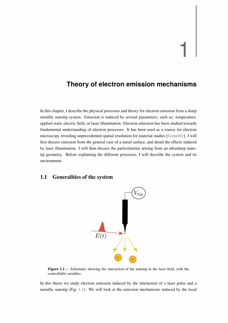
1.1 Generalities of the system
�� ��
Figure 1.1 – Schematic showing the interaction of the nanotip in the laser field, with the
controllable variables.
In this thesis we study electron emission induced by the interaction of a laser pulse and a
metallic nanotip (Fig. 1.1). We will look at the emission mechanisms induced by the local
temperature of the system (T [K]), the static electric field (F [V/m]), which is linked to the
applied tip bias (Vtip [V]) and nanotip size by the relation F “ βVtip [Gomer61], with β [m´1]
taking into account the tip geometry and the electric field of the laser E .
In this section I will introduce the system and the variables we use to describe it.
1.1.1 Electron potential at a metal/vacuum interface
The energy states of the electrons in a metallic system can be described according to the
Fermi-Dirac distribution. This distribution is given by
f pE,T q “ 1
1` exp´
E´μkbT
¯ , (1.1)
where T is the electron temperature, kB is the Boltzman constant, and μ is the Fermi energy.
The Fermi energy is the maximum energy an electron can have in a metal when the system
is at T “ 0 K. This equation refers to the number of electrons for a given energy E, where
E “ EK ` E‖. EK is the normal part of the kinetic energy and E‖ is the transverse. For
our system, what matters is the component that is normal to the surface, which is found by
integrating over the transverse components of the electron energy. Using the Sommerfeld
model of free electrons inside a metal, we get the electronic distribution
DpEK,T qdEK “ 4πmekBTh3
ln
ˆ1` exp
ˆμ´EK
kBT
˙˙dEK, (1.2)
where me is the mass of an electron and h is the Planck constant.
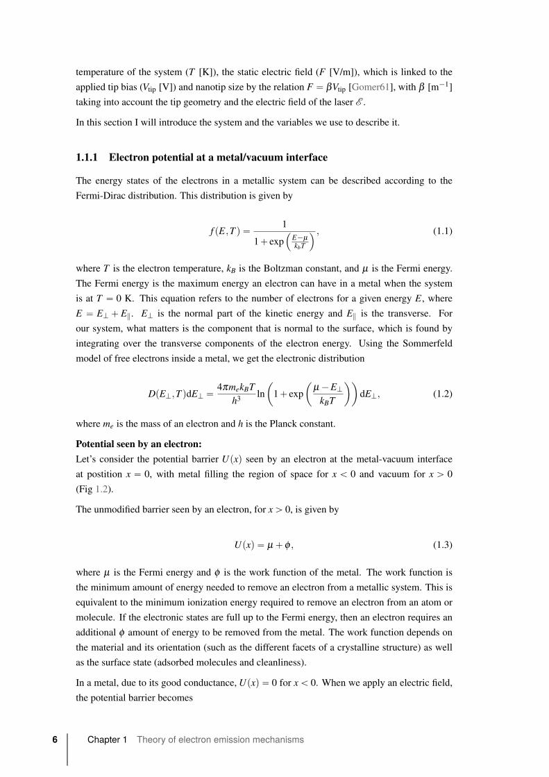
Potential seen by an electron:Let’s consider the potential barrier Upxq seen by an electron at the metal-vacuum interface
at postition x “ 0, with metal filling the region of space for x ă 0 and vacuum for x ą 0
(Fig 1.2).
The unmodified barrier seen by an electron, for xą 0, is given by
Upxq “ μ`φ , (1.3)
where μ is the Fermi energy and φ is the work function of the metal. The work function is
the minimum amount of energy needed to remove an electron from a metallic system. This is
equivalent to the minimum ionization energy required to remove an electron from an atom or
molecule. If the electronic states are full up to the Fermi energy, then an electron requires an
additional φ amount of energy to be removed from the metal. The work function depends on
the material and its orientation (such as the different facets of a crystalline structure) as well
as the surface state (adsorbed molecules and cleanliness).
In a metal, due to its good conductance, Upxq “ 0 for xă 0. When we apply an electric field,
the potential barrier becomes
6 Chapter 1 Theory of electron emission mechanisms
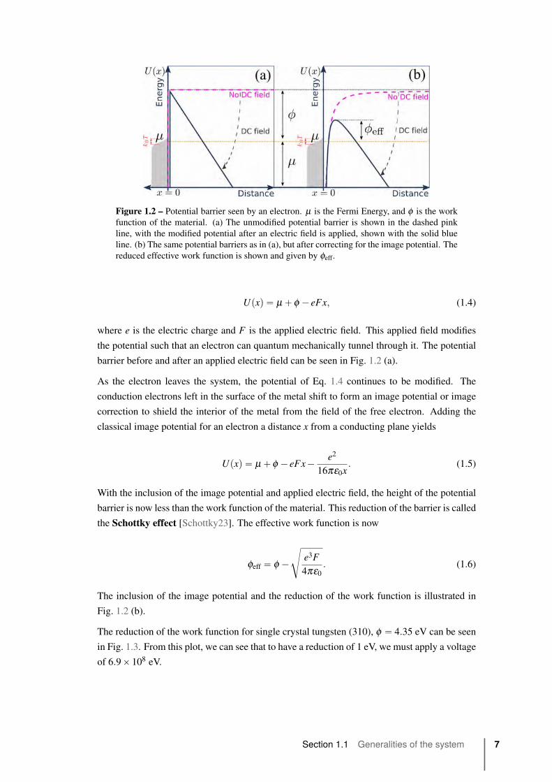
Figure 1.2 – Potential barrier seen by an electron. μ is the Fermi Energy, and φ is the work
function of the material. (a) The unmodified potential barrier is shown in the dashed pink
line, with the modified potential after an electric field is applied, shown with the solid blue
line. (b) The same potential barriers as in (a), but after correcting for the image potential. The
reduced effective work function is shown and given by φeff.
Upxq “ μ`φ ´ eFx, (1.4)
where e is the electric charge and F is the applied electric field. This applied field modifies
the potential such that an electron can quantum mechanically tunnel through it. The potential
barrier before and after an applied electric field can be seen in Fig. 1.2 (a).
As the electron leaves the system, the potential of Eq. 1.4 continues to be modified. The
conduction electrons left in the surface of the metal shift to form an image potential or image
correction to shield the interior of the metal from the field of the free electron. Adding the
classical image potential for an electron a distance x from a conducting plane yields
Upxq “ μ`φ ´ eFx´ e2
16πε0x. (1.5)
With the inclusion of the image potential and applied electric field, the height of the potential
barrier is now less than the work function of the material. This reduction of the barrier is called
the Schottky effect [Schottky23]. The effective work function is now
φeff “ φ ´d
e3F4πε0
. (1.6)
The inclusion of the image potential and the reduction of the work function is illustrated in
Fig. 1.2 (b).
The reduction of the work function for single crystal tungsten (310), φ “ 4.35 eV can be seen
in Fig. 1.3. From this plot, we can see that to have a reduction of 1 eV, we must apply a voltage
of 6.9ˆ108 eV.
Section 1.1 Generalities of the system 7

0 0.5 1 1.5 2x 10⁹
2.5
3
3.5
4
4.5
Applied Voltage (V)
Effe
ctiv
e W
ork
func
tion,
(eV)
Schottky Effect
Figure 1.3 – This shows effective work function from the Schottky effect as a function of the
applied DC electric field to the system.
1.1.2 Description of an ultrashort laser pulse
The laser light is described as an electric field which is the solution of Maxwell’s equations.
The complex electric field of an ultrashort laser pulse can be written as
Eptq “ Aptqeipω0t`Φptqqεεε, (1.7)
where Aptq is the temporal envelope of the pulse, ω0 is the frequency of the light, Φptq is thetemporal phase, and εεε is the laser polarization. For a Gaussian envelope, the real part of the
electric field becomes
ℜpE ptqq “ 1
2E0exp
ˆ´2ln2
t2
Δt2
˙¨ cospω0t`Φptqq , (1.8)
where E0 is the amplitude of the field and Δt is the pulse duration at full width at half maximum
(fwhm) of the intensity.
The temporal structure of an ultrashort pulse is easier to define in frequency space as the
Fourier transform of electric field
rE pωq “ rApωqeiϕpωq, (1.9)
where ϕpωq is the spectral phase of the pulse and rApωq is the spectral envelope. The spectral
phase can be expanded as a Taylor Expansion:
ϕpωq “ ϕpω0q`ϕ 1pω0qpω´ω0q` 1
2ϕ2pω0qpω´ω0q2` 1
6ϕ3pω0qpω´ω0q3 . . . , (1.10)
8 Chapter 1 Theory of electron emission mechanisms
in which ϕ describes the phase within the pulse envelope width of the carrier oscillation phase,
carrier envelope phase (CEP); the first order ϕ 1 describes the relative delay of the pulse; the
second order ϕ2 is the group delay dispersion (GDD) or chirp; the third order ϕ3 is the third
order dispersion (TOD).
The easiest way to conceptualize the temporal chirp of a pulse is to think about the relative
arrival time of the different frequency components of a pulse at a certain point in space. For
a pulse with a GDD of 0 (assuming all other dispersion orders are also 0), the frequency
components all arrive at the same time and the pulse duration is the minimum achievable as
determined by the time-bandwidth product. Since the speed of light in a material is dependent
on the wavelength of the light, as the pulse passes through a dispersive material the different
frequency components slow down respectively, thus arrive at our point in space at different
times, stretching out the pulse duration. A positively chirped pulse is one in which the lower
energy components (redder end of the spectrum) arrive before the higher energy components
(bluer end of the spectrum) and as such, with negatively chirped pulses the higher energy
components arrive first.
The relationship between the pulse duration and the spectral bandwidth can be given by the
energy-time uncertainty (recall the energy relation: E “ hω):
ΔωΔt ě 2πK, (1.11)
where Δω is the frequency bandwidth fwhm and K is a constant that depends on the pulse
envelope shape. For Gaussian pulses K “ 2ln2. This inequality defines a relationship between
the spectral bandwidth and minimum achievable pulse duration, i.e. the shorter the pulse
duration, the larger the spectral width and is known as the time-bandwidth product. As such,
the minimum pulse duration achievable, or Fourier transform or bandwidth limited pulse, is
given by:
Δt “ 2πKΔω
“ Kλ 20
cΔλ, (1.12)
where λ0 is the central wavelength of the pulse, Δλ is the wavelength bandwidth at fwhm,
and c is the speed of light in a vacuum with c “ 12π λω . Since fundamentally the relation-
ship is between energy and time, a higher energy overall allows for shorter pulses, and thus
less bandwidth is required to have equivalent pulse durations for pulses with a shorter central
wavelength.
In practice we measure the mean power of a laser. Given a repetition rate R of the laser, the
average power is
Pmean “ EˆR, (1.13)
where E is the pulse energy.
In our experimental setup we measure the spectrum, and pulse duration, energy per pulse,
mean power. The peak power of the laser pulse depends on the pulse duration, Δt, of the pulse
and is given by
Section 1.1 Generalities of the system 9
Ppeak “ EΔt“ Pmean
RΔt. (1.14)
With the spot size of the laser pΔxq2, we can also calculate the peak intensity.
Ipeak “ Ppeak
pΔxq2 . (1.15)
The cycle averaged intensity of the laser (I) is given by
I “ 1
2cε0E 2
0 , (1.16)
where ε0 is the permittivity of free space. From this we can calculate the amplitude of the
electric field of the laser E0.
1.1.3 Observables
We are interested in the electron emission mechanisms. The physical quantities that can be
measured are:
• emitted current
• energy distribution of emitted electrons
• spatial distribution of emitted electrons
• temporal aspects (however this is not discussed in this thesis)
1.1.4 Space charge effects
Space charge effects occur when more than one electron is emitted at the same time and are
then repelled from each other by Couloumb repulsion. The number of electrons emitted and
detected depends on many factors including the applied voltage and the laser intensity as
well as the geometrical constraints of the spectrometer and detector. For our experiment and
the theory presented in the rest of this chapter, we consider that there are no space charge
effects.
1.2 Mechanisms of electron emission
The emission of electrons from the surface of a condensed phase (generally a metallic surface)
into another phase (generally a vacuum) due to a high externally applied electric field is called
field emission [Good Jr56, Gomer61]. This means that when a high enough direct current (DC)
electric field is applied to the system, electrons can quantum mechanically tunnel through the
metal/vacuum interface. This interface forms a potential barrier through with electrons must
either tunnel through, or acquire enough energy to escape from the system. Field emission
was first observed and described by R.W. Wood in 1897 [Wood97], in which Wood describes a
10 Chapter 1 Theory of electron emission mechanisms

cathode discharge. W. Schottky, in 1923, described the mechanisms behind field emission, and
a connection between the applied field and a reduction in the height of the potential barrier (the
Schottky effect, Sec. 1.1.1) [Schottky23]. The emission current rate was described by Fowler
and Nordheim in 1928 [Fowler28] (Sec. 1.2.2). In the 1930s, E. W. Müller started using
field emission to study the surface properties of materials from nanotip based experiments
[Müller36]. From these experiments was developed the technique of exploiting the nanometer
sized termination from nanotip emitters to obtain high fields. This paved the path towards
field emission microscopy (FEM), scanning electron microscopy (SEM), and other techniques
[Gomer61].
1.2.1 Thermonic emission
Figure 1.4 – This shows the thermonic emission process where the system is heated enough
that some of the excited electrons have enough energy to overcome the work function and
classically escape. Note there is no externally applied DC field.
As the system heats up, the Fermi-Dirac distribution changes with temperature until a por-
tion of the electrons have sufficient energy to escape the work function. This is called ther-
monic emission. This process is governed by the Richardson-Dushman equation [Murphy56,
Herring49]
J “ AηT 2exp
ˆ´φkbT
˙, (1.17)
where J is the emitted current density, φ is the material work function, η is a material depen-
dent pre-factor and A is the Richardson constant defined as
A“ 4πmek2beh3
, (1.18)
where me is the mass of an electron, e is the charge of an electron and h is the Planck con-
stant. Note that in thermonic emission, there is no need for an externally applied electric field.
Instead, the system is heated enough such that some of the excited electrons have sufficient
energy to overcome the work function and classically escape from the metal [Lee73] as seen
in Fig. 1.4. The emission is governed by electrons whose energies are on the tail end of the
Section 1.2 Mechanisms of electron emission 11
Fermi-Dirac distribution and have energies greater than that of the barrier height. This means
that kbT must be on the order of φ . For single crystal W(310), with φ “ 4.35 eV, this corre-
sponds to a temperature of 5ˆ 104 K. This is historically the first emission which has been
observed experimentally, but we did not observe this process in our experiment as it requires
a very high temperature.
1.2.2 Cold field emission
Cold field emission is found to be extremely useful in electron microscopy as its spectrum is
spectrally coherent and yields a very narrow energy bandwidth [Gomer61, Murphy56]. The
theory present below describes field emission from a metal surface. Application of the nanotip
geometry is presented in Sec. 1.4.1.
A strongly applied electric field will create a finite potential barrier through which an electron
may quantum mechanically tunnel. In this case, calculations are made with an assumption that
the temperature is 0 K. This is called cold field emission. In cold field emission we apply a
large voltage to the system resulting in a large electric field, typically on the order of „1–10
GV/m. This enables electron tunneling emission.
Considering a Fermi-Dirac electron distribution, an electron has a probability PK to tunnel
through the potential barrier, the current density is given by J “ şE PK ¨DpEK,T qdEK, where
DpEK,T qdEK is the electron distribution given by Eq. 1.2.
The Fowler-Nordheim (FN) equation [Fowler28, Hommelhoff06b, Gomer61] describes the
emission current density from the system for an applied field, F , at 0 K
J 9 e3F2
4πhφ¨ exp
˜´4?2meφ 3{23heF
vpwq¸9 F2 ¨ exp
´´α
F
¯, (1.19)
with
α “ 4?2me
3heFvpwq ¨φ 3{2, (1.20)
and J is the current density of the emission, e is the electron charge, φ is the work function, me
is the electron mass, h is the reduced Planck constant and vpwq is a slowly varying function, the
Nordheim function [Murphy56, Hommelhoff06b, Gomer61], that takes into account the image
force of the tunneling electron (from the Schottky effect), with w, the Nordheim parameter
given by w“ e3{2a
F{4πε0{φ [Murphy56, Hommelhoff06b]. The function can be determined
by an iterative method described in [Gomer61]. The parameter w is simply the ratio between
the effective work function from the Schottky effect to the work function. At a low applied
field, there is minimal image force and vpwq “ 1. The Nordheim function is valued between
0.4 ă vpwq ă 0.8 [Hommelhoff06b] and can be determined by an iterative method described
in [Gomer61]. vpwq depends on the material and geometry of the tip. For our tungsten tips,
we use vpwq “ 0.6 [Hommelhoff06b].
12 Chapter 1 Theory of electron emission mechanisms
The FN equation relates the evolution of the current density to F . Since F is proportional
to the applied tip bias, Vtip, by a constant relating to the tip radius and material. The effects
of a nanotip geometry are explained in more detail in Sec. 1.4.1. Experimentally we can
plot ln´
J{V 2tip
¯as a function of 1{Vtip to determine the tip radius. This is discussed more in
Sec. 4.1.1.
1.2.3 Thermally enhanced field emission
Cold field emission is dominated by tunneling of electrons near the Fermi level of the system.
Likewise, thermonic emission is governed by electrons whose energies are on the tail end of the
Fermi-Dirac distribution and have energies greater than that of the barrier height. In between
these two processes is the regime of thermally enhanced field emission, where the electrons
are thermally excited, in our case, by laser light, but not enough to overcome the barrier and
instead are emitted via tunneling. This emission is caused by laser heating and for our purposes
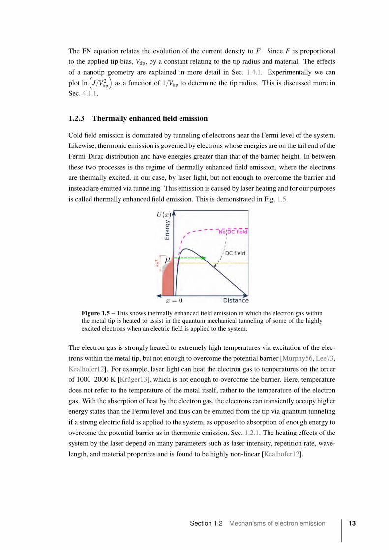
is called thermally enhanced field emission. This is demonstrated in Fig. 1.5.
Figure 1.5 – This shows thermally enhanced field emission in which the electron gas within
the metal tip is heated to assist in the quantum mechanical tunneling of some of the highly
excited electrons when an electric field is applied to the system.
The electron gas is strongly heated to extremely high temperatures via excitation of the elec-
trons within the metal tip, but not enough to overcome the potential barrier [Murphy56, Lee73,
Kealhofer12]. For example, laser light can heat the electron gas to temperatures on the order
of 1000–2000 K [Krüger13], which is not enough to overcome the barrier. Here, temperature
does not refer to the temperature of the metal itself, rather to the temperature of the electron
gas. With the absorption of heat by the electron gas, the electrons can transiently occupy higher
energy states than the Fermi level and thus can be emitted from the tip via quantum tunneling
if a strong electric field is applied to the system, as opposed to absorption of enough energy to
overcome the potential barrier as in thermonic emission, Sec. 1.2.1. The heating effects of the
system by the laser depend on many parameters such as laser intensity, repetition rate, wave-
length, and material properties and is found to be highly non-linear [Kealhofer12].
Section 1.2 Mechanisms of electron emission 13

1.3 Othermechanisms: emission processes induced by a laser field
Since the invention of lasers, laser-assisted electron emission from metallic surfaces has been
extensively studied [Lee73, Venus83]. This translates to the emission of electrons via the
absorption of energy quanta, or photons, of light and is analogous to the photoelectric ef-
fect [Einstein05]. Using continuous wave (cw) lasers, the process of photofield emission
(Sec. 1.3.1) was identified [Lee73, Venus83], in which energy from a laser is absorbed by
the system to promote an electron to a higher energy state and aid in tunneling. With the ad-
vent of ultrafast laser systems, the laser intensity can be greatly increased, and other emission
processes begin to dominate, namely above threshold photoemission and eventually optical
induced electron tunneling.
1.3.1 Photofield emission
Figure 1.6 – The system absorbs 1 photon, exciting the electrons, causing them to see an
effective barrier of φ 1eff “ φschottky´nhω promoting tunneling.
In photofield emission the system absorbs less photons than are needed to overcome the bar-
rier. With an externally applied electric field, a penetrable barrier is formed through which
electrons can tunnel as seen in Fig. 1.6. The emission rate can be described by the Fowler-
Nordheim equation (Eq. 1.19), with the work function replaced by the effective barrier height
φ 1eff “ φschottky´nhω , where φschottky is the effective work function described by the Schottky
reduction in Sec. 1.1.1 and n is the number of photons absorbed with nhω ă φ .
Photofield emission can be identified by comparing the emitted current from tips with and
without laser illumination [Hommelhoff06b]. Assuming the tip radius does not change, the
effective work function can be deduced from the FN equation. Photofield emission can also be
identified in the electron energy spectra by the asymetrical shape of the field emission and the
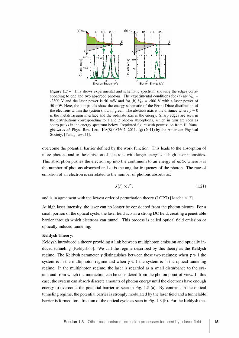
sharp edges around the energies of one-photon and two-photon absorptions [Yanagisawa11].
These one and two photon edges and asymetrical spectra can be seen in Fig. 1.7.
1.3.2 Intense laser induced emission processes
By increasing the laser intensity, the absorption of many photons is more likely, and it is
therefore possible for the system to absorb more photons than necessary for the electron to
14 Chapter 1 Theory of electron emission mechanisms
��� ���
Figure 1.7 – This shows experimental and schematic spectrum showing the edges corre-
sponding to one and two absorbed photons. The experimental conditions for (a) are Vtip =
-2300 V and the laser power is 50 mW and for (b) Vtip = -500 V with a laser power of
50 mW. Here, the top panels show the energy schematic of the Fermi-Dirac distribution of
the electrons within the system show in green. The abscissa axis is the distance where y“ 0
is the metal/vacuum interface and the ordinate axis is the energy. Sharp edges are seen in
the distributions corresponding to 1 and 2 photon absorptions, which in turn are seen as
sharp peaks in the energy spectrum below. Reprinted figure with permission from H. Yana-
gisawa et al. Phys. Rev. Lett. 108(8) 087602, 2011. c© (2011) by the American Physical
Society. [Yanagisawa11].
overcome the potential barrier defined by the work function. This leads to the absorption of
more photons and to the emission of electrons with larger energies at high laser intensities.
This absorption pushes the electron up into the continuum to an energy of nhω , where n is
the number of photons absorbed and ω is the angular frequency of the photon. The rate of
emission of an electron is correlated to the number of photons absorbs as:
JpIq 9 In, (1.21)
and is in agreement with the lowest order of perturbation theory (LOPT) [Joachain12].
At high laser intensity, the laser can no longer be considered from the photon picture. For a
small portion of the optical cycle, the laser field acts as a strong DC field, creating a penetrable
barrier through which electrons can tunnel. This process is called optical field emission or
optically induced tunneling.
Keldysh Theory:Keldysh introduced a theory providing a link between multiphoton emission and optically in-
duced tunneling [Keldysh65]. We call the regime described by this theory as the Keldysh
regime. The Keldysh parameter γ distinguishes between these two regimes; when γ " 1 the
system is in the multiphoton regime and when γ ! 1 the system is in the optical tunneling
regime. In the multiphoton regime, the laser is regarded as a small disturbance to the sys-
tem and from which the interaction can be considered from the photon point-of-view. In this
case, the system can absorb discrete amounts of photon energy until the electrons have enough
energy to overcome the potential barrier as seen in Fig. 1.8 (a). By contrast, in the optical
tunneling regime, the potential barrier is strongly modulated by the laser field and a tunnelable
barrier is formed for a fraction of the optical cycle as seen in Fig. 1.8 (b). For the Keldysh the-
Section 1.3 Other mechanisms: emission processes induced by a laser field 15

ory to be applicable, the photon energy from the laser must be smaller than the work function
of the metal, or ionization potential for an atom.
Figure 1.8 – (a) multiphoton regime, γ " 1 (b) tunneling regime, γ ! 1
The Keldysh parameter is given by
γ “d
φ2Up
, (1.22)
where φ is the work function of the material andUp is the ponderomotive energy. The pondero-
motive energy is the cycle-averaged quiver energy, or mean kinetic free energy, of an electron
oscillating in the electromagnetic field of a laser light field. Up is given by
Up “ e2E 20
4meω2, (1.23)
where e is the electron charge, me is the electron mass and E0 is the peak electric field of
the laser with frequency ω . Recalling the cycle-averaged laser intensity from Eq. 1.16, the
ponderomotive energy becomes
Up “ e2
2ε0meˆ I
ω29 Iλ 2. (1.24)
From this relation we can see that the tunneling regime (i.e. large Up) can be reached by either
increasing the laser intensity or decreasing its frequency. Emission from this regime is called
optical field emission.
The general rate of photoemission [Keldysh65, Bunkin65, Tóth91], Jpγq, derived from the
sum of all the contributions of photoemission from different multiphoton orders, can then be
given as
Jpγq 9 exp
ˆ´ 2φ
hω
ˆˆ1` 1
2γ2
˙asinhpγq´ 1
2γa
1` γ2
˙˙. (1.25)
This relation is applicable for all γ . The full derivation is found in [Bunkin65].
It is useful to express Eq. 1.25 in the limiting cases where γ " 1 and γ ! 1.
16 Chapter 1 Theory of electron emission mechanisms
Above Threshold Photoemission:In the case where γ ě 1, the case with small field amplitude, or large frequency, the system
can be thought of in the photon point of view. We have asinhpγq « lnp2γq giving
Jpγq 9 exp
ˆ´ 2φ
hωlnp2γq
˙9
ˆ1
2γ
˙2φ
hω 9 E2
φhω
0 . (1.26)
Recall from Eq. 1.16 that the intensity of the laser scales as E 20 of the laser field. This means
that the photocurrent is proportional to Inmin with nmin “ φ{hω , approximately the minimum
number of photons needed to overcome the potential barrier of the system. We can think of
the energy absorption of the system from the photon point of view.
The system absorbs n photons, increasing the energy by nhω . This pushes a portion of
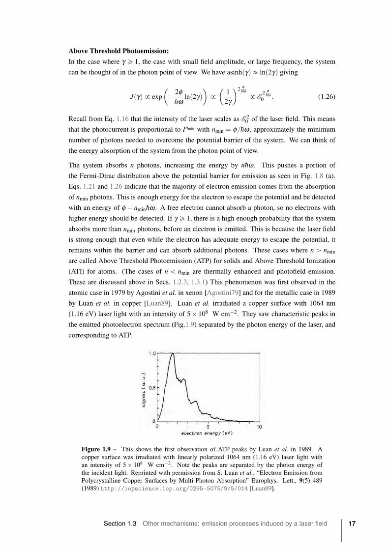
the Fermi-Dirac distribution above the potential barrier for emission as seen in Fig. 1.8 (a).
Eqs. 1.21 and 1.26 indicate that the majority of electron emission comes from the absorption
of nmin photons. This is enough energy for the electron to escape the potential and be detected
with an energy of φ ´ nminhω . A free electron cannot absorb a photon, so no electrons with
higher energy should be detected. If γ ě 1, there is a high enough probability that the system
absorbs more than nmin photons, before an electron is emitted. This is because the laser field
is strong enough that even while the electron has adequate energy to escape the potential, it
remains within the barrier and can absorb additional photons. These cases where n ą nmin
are called Above Threshold Photoemission (ATP) for solids and Above Threshold Ionization
(ATI) for atoms. (The cases of n ă nmin are thermally enhanced and photofield emission.
These are discussed above in Secs. 1.2.3, 1.3.1) This phenomenon was first observed in the
atomic case in 1979 by Agostini et al. in xenon [Agostini79] and for the metallic case in 1989
by Luan et al. in copper [Luan89]. Luan et al. irradiated a copper surface with 1064 nm
(1.16 eV) laser light with an intensity of 5ˆ 108 W cm´2. They saw characteristic peaks in
the emitted photoelectron spectrum (Fig.1.9) separated by the photon energy of the laser, and
corresponding to ATP.
Figure 1.9 – This shows the first observation of ATP peaks by Luan et al. in 1989. A
copper surface was irradiated with linearly polarized 1064 nm (1.16 eV) laser light with
an intensity of 5ˆ 108 W cm´2. Note the peaks are separated by the photon energy of
the incident light. Reprinted with permission from S. Luan et al., “Electron Emission from
Polycrystalline Copper Surfaces by Multi-Photon Absorption” Europhys. Lett., 9(5) 489
(1989) http://iopscience.iop.org/0295-5075/9/5/014 [Luan89].
Section 1.3 Other mechanisms: emission processes induced by a laser field 17
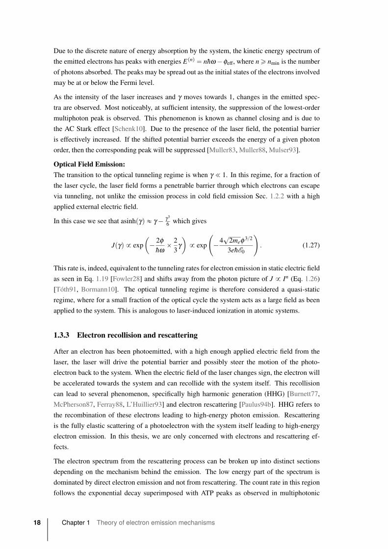
Due to the discrete nature of energy absorption by the system, the kinetic energy spectrum of
the emitted electrons has peaks with energies Epnq “ nhω´φeff, where ně nmin is the number
of photons absorbed. The peaks may be spread out as the initial states of the electrons involved
may be at or below the Fermi level.
As the intensity of the laser increases and γ moves towards 1, changes in the emitted spec-
tra are observed. Most noticeably, at sufficient intensity, the suppression of the lowest-order
multiphoton peak is observed. This phenomenon is known as channel closing and is due to
the AC Stark effect [Schenk10]. Due to the presence of the laser field, the potential barrier
is effectively increased. If the shifted potential barrier exceeds the energy of a given photon
order, then the corresponding peak will be suppressed [Muller83, Muller88, Mulser93].
Optical Field Emission:The transition to the optical tunneling regime is when γ ! 1. In this regime, for a fraction of
the laser cycle, the laser field forms a penetrable barrier through which electrons can escape
via tunneling, not unlike the emission process in cold field emission Sec. 1.2.2 with a high
applied external electric field.
In this case we see that asinhpγq « γ´ γ3
6which gives
Jpγq 9 exp
ˆ´ 2φ
hωˆ 2
3γ˙9 exp
˜´4?2meφ 3{23ehE0
¸. (1.27)
This rate is, indeed, equivalent to the tunneling rates for electron emission in static electric field
as seen in Eq. 1.19 [Fowler28] and shifts away from the photon picture of J 9 In (Eq. 1.26)
[Tóth91, Bormann10]. The optical tunneling regime is therefore considered a quasi-static
regime, where for a small fraction of the optical cycle the system acts as a large field as been
applied to the system. This is analogous to laser-induced ionization in atomic systems.
1.3.3 Electron recollision and rescattering
After an electron has been photoemitted, with a high enough applied electric field from the
laser, the laser will drive the potential barrier and possibly steer the motion of the photo-
electron back to the system. When the electric field of the laser changes sign, the electron will
be accelerated towards the system and can recollide with the system itself. This recollision
can lead to several phenomenon, specifically high harmonic generation (HHG) [Burnett77,
McPherson87, Ferray88, L’Huillier93] and electron rescattering [Paulus94b]. HHG refers to
the recombination of these electrons leading to high-energy photon emission. Rescattering
is the fully elastic scattering of a photoelectron with the system itself leading to high-energy
electron emission. In this thesis, we are only concerned with electrons and rescattering ef-
fects.
The electron spectrum from the rescattering process can be broken up into distinct sections
depending on the mechanism behind the emission. The low energy part of the spectrum is
dominated by direct electron emission and not from rescattering. The count rate in this region
follows the exponential decay superimposed with ATP peaks as observed in multiphotonic
18 Chapter 1 Theory of electron emission mechanisms
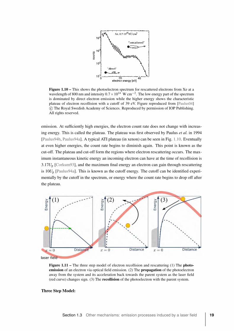
Figure 1.10 – This shows the photoelectron spectrum for rescattered electrons from Xe at a
wavelength of 800 nm and intensity 0.7ˆ1014 W cm´2. The low energy part of the spectrum
is dominated by direct electron emission while the higher energy shows the characteristic
plateau of electron recollision with a cutoff of 39 eV. Figure reproduced from [Paulus04]c© The Royal Swedish Academy of Sciences. Reproduced by permission of IOP Publishing.
All rights reserved.
emission. At sufficiently high energies, the electron count rate does not change with increas-
ing energy. This is called the plateau. The plateau was first observed by Paulus et al. in 1994
[Paulus94b, Paulus94a]. A typical ATI plateau (in xenon) can be seen in Fig. 1.10. Eventually
at even higher energies, the count rate begins to diminish again. This point is known as the
cut-off. The plateau and cut-off form the regions where electron rescattering occurs. The max-
imum instantaneous kinetic energy an incoming electron can have at the time of recollision is
3.17Up [Corkum93], and the maximum final energy an electron can gain through rescattering
is 10Up [Paulus94a]. This is known as the cutoff energy. The cutoff can be identified experi-
mentally by the cutoff in the spectrum, or energy where the count rate begins to drop off after
the plateau.
Figure 1.11 – The three step model of electron recollision and rescattering (1) The photo-emission of an electron via optical field emission. (2) The propagation of the photoelectron
away from the system and its acceleration back towards the parent system as the laser field
(red curve) changes sign. (3) The recollision of the photoelectron with the parent system.
Three Step Model:
Section 1.3 Other mechanisms: emission processes induced by a laser field 19
The rescattering process can be easily envisioned using the Three Step Model (TSM), formu-
lated by Paul Corkum in 1993 [Corkum93]. The three steps are given as:
1. Photoemission of an electron generally via tunneling in optical field emission
2. Propagation of the photoelectron away from system and then acceleration back towards
the system as the field changes sign
3. Recollision of the photoelectron with the parent system. Many physical phenomena are
possible at this stage such as recombination and reabsorption with the parent system
itself, however we are only concerned with recollision and rescattering of the photo-
electron with the parent system in this thesis
By applying Eq. 1.23 to Eq. 1.22, we can rewrite the Keldysh parameter as the ratio of two
frequencies
γ “ ωωt
, (1.28)
where ω is the optical driving frequency of the laser and ωt is a characteristic tunneling fre-
quency given by ωt “ eE0{?2meφ [Herink12]. The parameter can be thought of as an adia-
baticity parameter to define the different photoemission regimes. As discussed in above the
resulting electron movement in the driving field, and energy cutoff, scale with the ponderomo-
tive energy, Up (Eq. 1.23), forming the first two steps of the three step model.
1.4 Peculiarities arising from a nanotip geometry
The laser emission phenomenon described thus far hold true for atomic systems and metallic
surfaces [Joachain12], however we must take into account that in this thesis, investigations
are on photoemission from nanotip systems. As such, the geometry of these systems must
be taken into account when considering the applied DC field as well as optical field from the
laser.
1.4.1 Geometric field enhancement
To achieve cold field emission by applying reasonable voltages, etched field emission nanotips
are generally used, which have a half-sphere termination on a nanometer size. This is due to
the accumulation of charge within the surface apex of the tip, called the lightning rod effect.
For tips, the field at the end of the apex is given by
F “ βVtip, (1.29)
whereVtip is the applied voltage, and β is related to the tip radius r with β “ 1{kr, with k being
a dimensionless factor depending on the shape of the tip and the extraction geometry typically
on the order of k „ 5 near the apex [Gomer61]. β can be thought of as the field amplification
factor and can reach factors varying from 106 to 107 m´1 from tip to tip. Thus, the high fields
needed to achieve emission can be enhanced geometrically by the sharpness of the tips.
20 Chapter 1 Theory of electron emission mechanisms
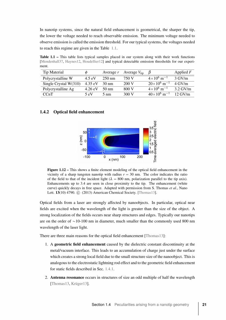
In nanotip systems, since the natural field enhancement is geometrical, the sharper the tip,
the lower the voltage needed to reach observable emission. The minimum voltage needed to
observe emission is called the emission threshold. For our typical systems, the voltages needed
to reach this regime are given in the Table 1.1.
Table 1.1 – This table lists typical samples placed in our system along with their work functions
[Mendenhall37, Haynes12, Houdellier12] and typical detectable emission thresholds for our experi-
ment.
Tip Material φ Average r Average Vtip β Applied F
Polycrystalline W 4.5 eV 250 nm 750 V 4ˆ106 m´1 3 GV/m
Single Crystal W(310) 4.35 eV 30 nm 200 V 20ˆ106 m´1 4 GV/m
Polycrystalline Ag 4.26 eV 50 nm 800 V 4ˆ106 m´1 3.2 GV/m
CCnT 5 eV 5 nm 300 V 40ˆ106 m´1 12 GV/m
1.4.2 Optical field enhancement
Figure 1.12 – This shows a finite element modeling of the optical field enhancement in the
vicinity of a sharp tungsten nanotip with radius r “ 30 nm. The color indicates the ratio
of the field to that of the incident light (λ “ 800 nm, polarization parallel to the tip axis).
Enhancements up to 3.4 are seen in close proximity to the tip. The enhancement (white
curve) quickly decays in free space. Adapted with permission from S. Thomas et al., Nano
Lett. 13(10) 4790. c© (2013) American Chemical Society. [Thomas13].
Optical fields from a laser are strongly affected by nanoobjects. In particular, optical near
fields are excited when the wavelength of the light is greater than the size of the object. A
strong localization of the fields occurs near sharp structures and edges. Typically our nanotips
are on the order of „10-100 nm in diameter, much smaller than the commonly used 800 nm
wavelength of the laser light.
There are three main reasons for the optical field enhancement [Thomas13]:
1. A geometric field enhancement caused by the dielectric constant discontinuity at the
metal/vacuum interface. This leads to an accumulation of charge just under the surface
which creates a strong local field due to the small structure size of the nanoobject. This is
analogous to the electrostatic lightning rod effect and to the geometric field enhancement
for static fields described in Sec. 1.4.1.
2. Antenna resonance occurs in structures of size an odd multiple of half the wavelength
[Thomas13, Krüger13].
Section 1.4 Peculiarities arising from a nanotip geometry 21

3. Plasmonic effects in plasmonic materials such as silver or gold create a surface or plas-
mon resonance when the optical frequency is close to the resonance frequency of the
plasmon [Sasaki13, Stockman11]. These resonances are highly material, shape and
wavelength dependent.
This means that the typical laser intensities needed to reach the strong-field regime are greatly
reduced due to optical field enhancement and the need for an amplified laser chain is much
less.
The optical field enhancement in the vicinity of a sharp tungsten nanotip, with radius r “30 nm can be calculated using finite element modeling. This is seen in Fig. 1.12 (calculation
performed by [Thomas13]). The tip is illuminated with a laser pulse of wavelength 800 nm and
polarization parallel to the tip axis. From this we that the optical field of the laser is enhance
up to 3.4 in close proximity of the tip. This enhancement exponentially decays away in free
space. Inside the tip, the metal is nearly field free.
The optical field enhancement depends on the both the geometry of the tip and its material.
Gold and Silver have plasmonic resonances in the visible domain, which lead to higher field
enhancement [Arbouet12]. The radius of the tip and the opening angle also greatly influence
the field enhancement. A smaller radius tip has higher enhancement, as discussed above,
but the dependence of the angle is not straightforward. In [Thomas14], Thomas (group of
P. Hommelhoff) calculated that there is an optimal angle for which the field enhancement is
highest. For tungsten, this is a half opening angle of 30˝; for gold it is 15˝.
1.4.3 Facet emission
The metallic nature of tip means that the atoms in the tip are oriented in a crystalline structure.
Each crystal orientation has a slightly different work function [Mendenhall37, Haynes12], and
thus electron emission is easier or harder from a particular orientation. In an etched nanotip,
this corresponds to each side, or facet, having a different crystal orientation. Etching a nanotip
from a single crystal oriented wire ensures the location of each facet orientation with respect
to the detector.
Figure 1.13 – (a) This shows emission sites from a (011) oriented W nanotip illustrating
that the (310) facet has the most intense electron emission. The schematic shows the crystal
facet orientations of the nanotip. (b) This shows the emission patterns with laser irradiation.
The schematic shows the side view of the laser-induced field-emission geometry. Reprinted
figure with permission from H. Yanagisawa et al. Phys. Rev. Lett. 103(25) 257603, 2009.c© (2009) by the American Physical Society. [Yanagisawa09]
22 Chapter 1 Theory of electron emission mechanisms

In tungsten, the (310) orientation has the lowest work function [Mendenhall37]. In Fig. 1.13 (a),
Yanagisawa et al. [Yanagisawa09, Yanagisawa10] show that the most intense electron emis-
sion comes from the (310) oriented facets. When illuminated by a laser (Fig.1.13 (b)), the
emission pattern becomes strongly asymmetrical. Here the most intense emission is opposite
the exposed side relative to the laser incidence. As the (310) orientation yields the bright-
est electron emission, we chose to etch our tungsten nanotips out of single crystal tungsten
oriented in the (310) direction such that the bright emission site is oriented towards the detec-
tor.
1.4.4 Electron propagation in the vicinity of a nanotip
Let us consider an electron after it has left the system, traveling in the electric field of a
laser in the vicinity of the sharp nanotip. Due to the sub-wavelength size of nanostructures,
and in particular our nanotips, the optical fields interacting with, and around these structures
vary greatly (Sec. 1.4.2) such that the resulting electron dynamics may be quite unexpected
[Herink12].
Herink et al. (group of C. Ropers) [Herink12] investigated the cutoff energy of electrons from
a gold nanotip as a function of laser wavelength (and by consequence Up). Recall the pon-
deromotive energy, is the cycle-averaged quiver energy of an electron in an electric field. The
quiver motion, or excursion, is the amplitude of a free electron in the electric field of a laser
[Joachain12]. This motion is given by
lq “ eE0
meω2. (1.30)
At longer wavelengths, Herink et al. observed the convergence of the cutoff energies. This
is because the quiver motion of the emitted electrons extends beyond the decay length of
the optical field („ 1{4 the tip radius) [Herink12]. We can now define a new adiabaticity
parameter, δ , relating the (1/e)-decay length lE0of the optical field to the quiver amplitude
as
δ “ lE0
lq“ lE0
meω2
eE0. (1.31)
While the Keldysh parameter describe the emission process of the electron from the system
(step 1 in the TSM), δ describes the propagation and acceleration of the electron once emitted
from the system (step 2 in the TSM) [Herink12]. For δ " 1, the quiver regime, the electron
oscillates in a nearly homogeneous field for multiple optical cycles, as described for “normal”
electron propagation. For δ ! 1, the sub-cycle regime, the electron rapidly escapes the tip-
enhanced field in a time much shorter than an optical cycle as seen in Fig. 1.14.
This effect is corroborated by Park et al. (group of C. Lienau) [Park12] who observed a pro-
nounced acceleration of electrons within the field gradient of their nanotip for long wave-
lengths. They found that in the sub-cycle δ ! 1 regime, angle-dependent kinetic energy spec-
tra revealed a narrowing of the emission cone for fast emission, ascribed to the fast escape of
the electrons from the modified field. This is attributed field-induced steering of these sub-
cycle electrons, as opposed to the divergent quiver motion of the δ " 1 regime. The results of
Section 1.4 Peculiarities arising from a nanotip geometry 23
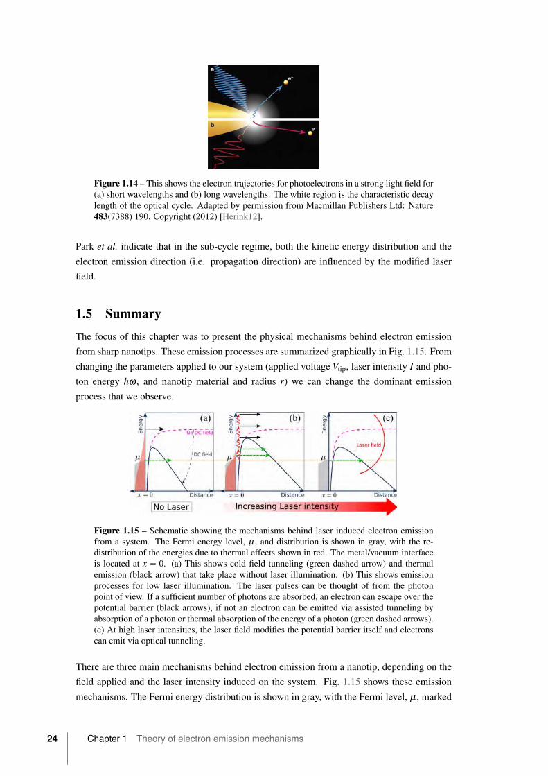
Figure 1.14 – This shows the electron trajectories for photoelectrons in a strong light field for
(a) short wavelengths and (b) long wavelengths. The white region is the characteristic decay
length of the optical cycle. Adapted by permission from Macmillan Publishers Ltd: Nature
483(7388) 190. Copyright (2012) [Herink12].
Park et al. indicate that in the sub-cycle regime, both the kinetic energy distribution and the
electron emission direction (i.e. propagation direction) are influenced by the modified laser
field.
1.5 Summary
The focus of this chapter was to present the physical mechanisms behind electron emission
from sharp nanotips. These emission processes are summarized graphically in Fig. 1.15. From
changing the parameters applied to our system (applied voltage Vtip, laser intensity I and pho-
ton energy hω , and nanotip material and radius r) we can change the dominant emission
process that we observe.
Figure 1.15 – Schematic showing the mechanisms behind laser induced electron emission
from a system. The Fermi energy level, μ , and distribution is shown in gray, with the re-
distribution of the energies due to thermal effects shown in red. The metal/vacuum interface
is located at x “ 0. (a) This shows cold field tunneling (green dashed arrow) and thermal
emission (black arrow) that take place without laser illumination. (b) This shows emission
processes for low laser illumination. The laser pulses can be thought of from the photon
point of view. If a sufficient number of photons are absorbed, an electron can escape over the
potential barrier (black arrows), if not an electron can be emitted via assisted tunneling by
absorption of a photon or thermal absorption of the energy of a photon (green dashed arrows).
(c) At high laser intensities, the laser field modifies the potential barrier itself and electrons
can emit via optical tunneling.
There are three main mechanisms behind electron emission from a nanotip, depending on the
field applied and the laser intensity induced on the system. Fig. 1.15 shows these emission
mechanisms. The Fermi energy distribution is shown in gray, with the Fermi level, μ , marked
24 Chapter 1 Theory of electron emission mechanisms
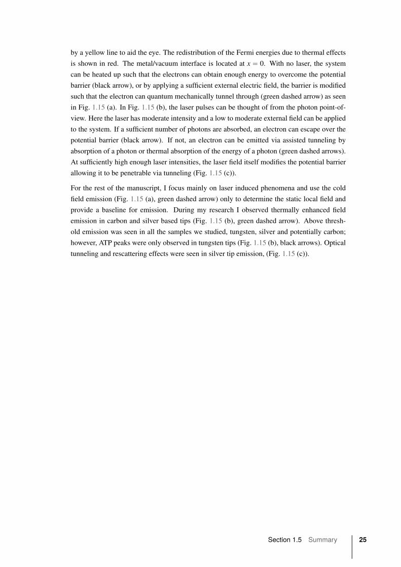
by a yellow line to aid the eye. The redistribution of the Fermi energies due to thermal effects
is shown in red. The metal/vacuum interface is located at x “ 0. With no laser, the system
can be heated up such that the electrons can obtain enough energy to overcome the potential
barrier (black arrow), or by applying a sufficient external electric field, the barrier is modified
such that the electron can quantum mechanically tunnel through (green dashed arrow) as seen
in Fig. 1.15 (a). In Fig. 1.15 (b), the laser pulses can be thought of from the photon point-of-
view. Here the laser has moderate intensity and a low to moderate external field can be applied
to the system. If a sufficient number of photons are absorbed, an electron can escape over the
potential barrier (black arrow). If not, an electron can be emitted via assisted tunneling by
absorption of a photon or thermal absorption of the energy of a photon (green dashed arrows).
At sufficiently high enough laser intensities, the laser field itself modifies the potential barrier
allowing it to be penetrable via tunneling (Fig. 1.15 (c)).
For the rest of the manuscript, I focus mainly on laser induced phenomena and use the cold
field emission (Fig. 1.15 (a), green dashed arrow) only to determine the static local field and
provide a baseline for emission. During my research I observed thermally enhanced field
emission in carbon and silver based tips (Fig. 1.15 (b), green dashed arrow). Above thresh-
old emission was seen in all the samples we studied, tungsten, silver and potentially carbon;
however, ATP peaks were only observed in tungsten tips (Fig. 1.15 (b), black arrows). Optical
tunneling and rescattering effects were seen in silver tip emission, (Fig. 1.15 (c)).
Section 1.5 Summary 25

2Optical setup and development of a NOPA
The colours red, blue and green are real. The colouryellow is a mystical experience shared by everybody.
– Tom Stoppard,
Rosencrantz & Guildenstern are Dead
To investigate the emission of electrons from a nanotip induced by a laser field, there are
certain requirements that must be met by the system. We need a short pulse duration to avoid
thermal effects created by the laser as well as the high peak power associated with such short
pulses. We also would like a high repetition rate to have the best signal to noise ratio possible.
As such, the laser system went through much evolution. In general, the system is very versatile
involving many different elements from a commercially available laser amplification chain to
home made laser development. The first setup uses the traditional ultrafast laser amplification
chain, an Ti:sapphire femtosecond oscillator at 62 MHz with the ability to be amplified in
energy via a regenerative amplifier at 1 kHz. The next generation laser source is a variable
repetition rate (from single shot to 2 MHz) infrared (IR) fiber laser with a non-collinear optical
parametric amplifying (NOPA) stage, which allows us the opportunity to keep the duration
short and both vary the repetition rate of the laser as well as the wavelength.
In this chapter I will first detail the conventional Ti:sapphire laser system and amplification
chain that was used for the results in this thesis. I describe the laser characterization that
is needed to interpret the data. Finally I discuss the NOPA development required to further
clarify and augment our conclusions.
2.1 Optical setup
In this section I explain the optical setup of the experiment that was used in the research
I present in this thesis. I describe the Ti:sapphire laser system and amplification chain as
well as the diagnostics and characterization necessary for understanding the physics of the
interaction.
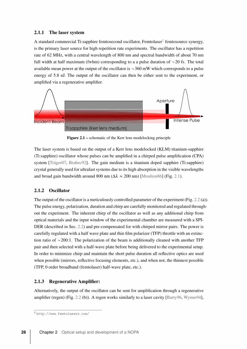
2.1.1 The laser system
A standard commercial Ti:sapphire femtosecond oscillator, Femtolaser1 femtosource synergy,
is the primary laser source for high repetition rate experiments. The oscillator has a repetition
rate of 62 MHz, with a central wavelength of 800 nm and spectral bandwidth of about 70 nm
full width at half maximum (fwhm) corresponding to a a pulse duration of „20 fs. The total
available mean power at the output of the oscillator is„360 mW which corresponds to a pulse
energy of 5.8 nJ. The output of the oscillator can then be either sent to the experiment, or
amplified via a regenerative amplifier.
��������
Figure 2.1 – schematic of the Kerr lens modelocking principle
The laser system is based on the output of a Kerr lens modelocked (KLM) titanium-sapphire
(Ti:sapphire) oscillator whose pulses can be amplified in a chirped pulse amplification (CPA)
system [Träger07, Brabec92]. The gain medium is a titanium doped sapphire (Ti:sapphire)
crystal generally used for ultrafast systems due to its high absorption in the visible wavelengths
and broad gain bandwidth around 800 nm (Δλ « 200 nm) [Moulton86] (Fig. 2.1).
2.1.2 Oscillator
The output of the oscillator is a meticulously controlled parameter of the experiment (Fig. 2.2 (a)).
The pulse energy, polarization, duration and chirp are carefully monitored and regulated through-
out the experiment. The inherent chirp of the oscillator as well as any additional chirp from
optical materials and the input window of the experimental chamber are measured with a SPI-
DER (described in Sec. 2.2) and pre-compensated for with chirped mirror pairs. The power is
carefully regulated with a half wave plate and thin film polarizer (TFP) throttle with an extinc-
tion ratio of „200:1. The polarization of the beam is additionally cleaned with another TFP
pair and then selected with a half-wave plate before being delivered to the experimental setup.
In order to minimize chirp and maintain the short pulse duration all reflective optics are used
when possible (mirrors, reflective focusing elements, etc.), and when not, the thinnest possible
(TFP, 0 order broadband (femtolaser) half-wave plate, etc.).
2.1.3 Regenerative Amplifier:
Alternatively, the output of the oscillator can be sent for amplification through a regenerative
amplifier (regen) (Fig. 2.2 (b)). A regen works similarly to a laser cavity [Barty96, Wynne94],
1 http://www.femtolasers.com/
28 Chapter 2 Optical setup and development of a NOPA
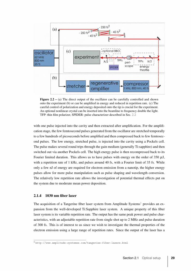
Figure 2.2 – (a) The direct output of the oscillator can be carefully controlled and shown
onto the experiment (b) or can be amplified in energy and reduced in repetition rate. (c) The
careful control of polarization and energy deposited onto the tip is crucial for the experiment.
An optional nonlinear crystal can be inserted into the beamline to frequency double the light.
TFP: thin film polarizer, SPIDER: pulse characterizer described in Sec. 2.2
with one pulse injected into the cavity and then extracted after amplification. For the amplifi-
cation stage, the few femtosecond pulses generated from the oscillator are stretched temporally
to a few hundreds of picoseconds before amplified and then compressed back to few femtosec-
ond pulses. The low energy, stretched pulse, is injected into the cavity using a Pockels cell.
The pulse makes several round trips through the gain medium (generally Ti:sapphire) and then
switched out via another Pockels cell. The high energy pulse is then recompressed back to its
Fourier limited duration. This allows us to have pulses with energy on the order of 350 μJ,
with a repetition rate of 1 kHz, and pulses around 40 fs, with a Fourier limit of 35 fs. While
only a few nJ of energy are required for electron emission from a nanotip, the higher energy
pulses allow for more pulse manipulation such as pulse shaping and wavelength conversion.
The relatively low repetition rate allows the investigation of potential thermal effects put on
the system due to moderate mean power deposition.
2.1.4 1030 nm fiber laser
The acquisition of a Tangerine fiber laser system from Amplitude Systems1 provides an ex-
pansion from the well-developed Ti:Sapphire laser system. A unique property of this fiber
laser system is its variable repetition rate. The output has the same peak power and pulse char-
acteristics, with an adjustable repetition rate from single shot up to 2 MHz and pulse duration
of 300 fs. This is of interest to us since we wish to investigate the thermal properties of the
electron emission using a large range of repetition rates. Since the output of the laser has a
1 http://www.amplitude-systemes.com/tangerine-fiber-lasers.html
Section 2.1 Optical setup 29
central wavelength of 1030 nm, and a pulse duration of 300 fs, a NOPA stage is built to allow
for short pulses and flexibility in wavelength. The NOPA is described in Sec. 2.3
2.2 Laser characterization diagnostics
The correct characterization of the laser pulses is vital to understanding its effects on the
system. As the processes are often intensity dependent, this means that careful measuring
of the laser spot size, pulse duration and pulse energy that are needed to evaluate the laser
intensity (in W cm´2) that illuminate the nanotips.
2.2.1 Spot Size Characterization
For a Gaussian beam, the 1{e2 radius (where e is Euler’s number) of the intensity, w, for a
beam of wavelength λ is given as function of beam propagation, x, where
wpxq “ w0
dˆ1` x2
x2R
˙, (2.1)
and xR is the Rayleigh range given by
xR “ πw20
λ, (2.2)
and is defined as the positions where wpxq ă ?2w0. The beam is narrowest at position z “ 0
and this position is called the beam waist and has a size of w0. For a focus of length f , w0 can
be found by
2w0 “ˆ4λπ
˙ˆfD
˙, (2.3)
where D is the diameter illuminated on the lens, in other words, the collimated 1{e2 di-
ameter of the laser beam before focusing. The derivation of this relation can be found in
Ref. [Saleh07].
The beam is never a perfect Gaussian, nor is it perfectly focused, so measuring the beam
diameter is necessary. The easiest method of spot size measurement is to directly focus the
laser onto a beam profiling charge-coupled device (CCD) camera and to measure the spot size
from the image produced. However, the geometrical constraints of our optical setup due to the
focusing elements – on-axis spherical mirror and off-axis parabolas (OAP) – and small focal
length do not allow us to characterize the focus spot size with a beam profiler. Instead we turn
to other means of spot size measurement, such as a knife edge measurement.
In a knife edge measurement, the intensity of the beam is measured as a function of the position
of the translation of a sharp edge (a knife or razor blade) as it passes through the beam. If the
edge passes through the focus, a 1-dimensional measurement of the focus spot size is recorded.
30 Chapter 2 Optical setup and development of a NOPA
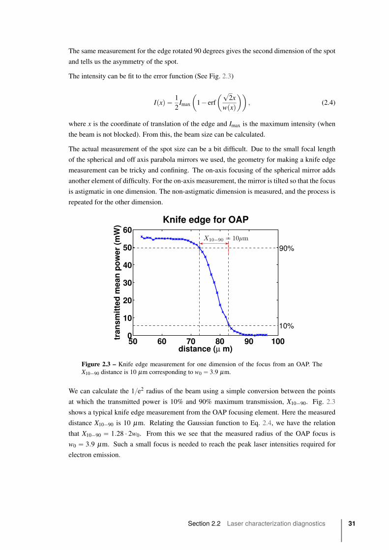
The same measurement for the edge rotated 90 degrees gives the second dimension of the spot
and tells us the asymmetry of the spot.
The intensity can be fit to the error function (See Fig. 2.3)
Ipxq “ 1
2Imax
ˆ1´ erf
ˆ?2x
wpxq˙˙
, (2.4)
where x is the coordinate of translation of the edge and Imax is the maximum intensity (when
the beam is not blocked). From this, the beam size can be calculated.
The actual measurement of the spot size can be a bit difficult. Due to the small focal length
of the spherical and off axis parabola mirrors we used, the geometry for making a knife edge
measurement can be tricky and confining. The on-axis focusing of the spherical mirror adds
another element of difficulty. For the on-axis measurement, the mirror is tilted so that the focus
is astigmatic in one dimension. The non-astigmatic dimension is measured, and the process is
repeated for the other dimension.
50 60 70 80 90 1000
10
20
30
40
50
60
Knife edge for OAP
tran
sm
itte
d m
ean
po
wer
(mW
)
distance (μ m)
90%
10%
Figure 2.3 – Knife edge measurement for one dimension of the focus from an OAP. The
X10´90 distance is 10 μm corresponding to w0 “ 3.9 μm.
We can calculate the 1{e2 radius of the beam using a simple conversion between the points
at which the transmitted power is 10% and 90% maximum transmission, X10´90. Fig. 2.3
shows a typical knife edge measurement from the OAP focusing element. Here the measured
distance X10´90 is 10 μm. Relating the Gaussian function to Eq. 2.4, we have the relation
that X10´90 “ 1.28 ¨ 2w0. From this we see that the measured radius of the OAP focus is
w0 “ 3.9 μm. Such a small focus is needed to reach the peak laser intensities required for
electron emission.
Section 2.2 Laser characterization diagnostics 31
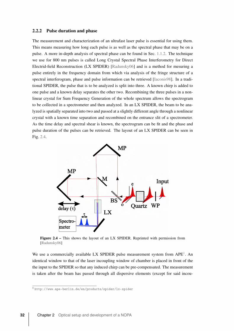
2.2.2 Pulse duration and phase
The measurement and characterization of an ultrafast laser pulse is essential for using them.
This means measuring how long each pulse is as well as the spectral phase that may be on a
pulse. A more in-depth analysis of spectral phase can be found in Sec. 1.1.2. The technique
we use for 800 nm pulses is called Long Crystal Spectral Phase Interferometry for Direct
Electrid-field Reconstruction (LX SPIDER) [Radunsky06] and is a method for mesuring a
pulse entirely in the frequency domain from which via analysis of the fringe structure of a
spectral interferogram, phase and pulse information can be retrieved [Iaconis98]. In a tradi-
tional SPIDER, the pulse that is to be analyzed is split into three. A known chirp is added to
one pulse and a known delay separates the other two. Recombining the three pulses in a non-
linear crystal for Sum Frequency Generation of the whole spectrum allows the spectrogram
to be collected in a spectrometer and then analyzed. In an LX SPIDER, the beam to be ana-
lyzed is spatially separated into two and passed at a slightly different angle through a nonlinear
crystal with a known time separation and recombined on the entrance slit of a spectrometer.
As the time delay and spectral shear is known, the spectrogram can be fit and the phase and
pulse duration of the pulses can be retrieved. The layout of an LX SPIDER can be seen in
Fig. 2.4.
Figure 2.4 – This shows the layout of an LX SPIDER. Reprinted with permission from
[Radunsky06]
We use a commercially available LX SPIDER pulse measurement system from APE1. An
identical window to that of the laser incoupling window of chamber is placed in front of the
the input to the SPIDER so that any induced chirp can be pre-compensated. The measurement
is taken after the beam has passed through all dispersive elements (except for said incou-
1 http://www.ape-berlin.de/en/products/spider/lx-spider
32 Chapter 2 Optical setup and development of a NOPA
pling window) so that the exact characterization of the pulses that arrive on the nanotip is
known.
2.2.3 Peak Intensity
In general when discussing ultrafast laser pulses, terms such as “pulse energy,” and “peak
intensity” are used, but the measurement of such is not evident. For low repetition lasers,
such as the 1 kHz amplified pulses, the pulse energy can be directly measured using an energy
meter. From this measurement, along with the spot size and pulse duration, the peak intensity
for one pulse, can be calculated.
Ipeak “ 2EΔtπw2
0
, (2.5)
where E is the pulse energy, Δt is the pulse duration and πw20 is the spot size.
For high repetition lasers, such as those from the oscillator, direct measurement of the pulse
energy is not possible because the pulses are too close temporally. Instead the average power
is measured which includes the time between pulses when the energy is 0. Thus to calculate
the peak intensity, and pulse energy one must also take into account the repetition rate of the
laser as well as pulse duration and spot size.
Ipeak “ 2Pmean
RΔtπw20
, (2.6)
where R is the repetition rate of the laser.
2.3 Noncollinear Optical Parametric Amplifier (NOPA)
While the use of the traditional laser chain has great utility and flexibility in the types of exper-
iments that can be done with our setup, further investigations into mean power and wavelength
dependent effects were of interest to me during my thesis research. As such, we acquired an
infrared fiber laser system which allows a variability in repetition rate, from single shot to
several tens of MHz, while maintaining the same output peak power. The drawback of such a
fiber system is long pulse duration, 300 fs. In order to have access to the short pulse duration
needed, we built a Noncollinear Optical Parametric Amplification (NOPA) stage at the output
[Cerullo03]. This laser source has both fine tuning capabilities in wavelength and repetition
rate as well as a short output.
The high peak power of ultrafast laser systems has led to the use of Optical Parametric Ampli-
fication (OPA) which allows the fundamental wavelength to be transformed and amplified into
any color from the visible to mid-infrared. In order to compare our results with those from
the oscillator and regen interaction, as well as to use the same optical setup, we first center the
output of the NOPA at 800 nm.
Section 2.3 Noncollinear Optical Parametric Amplifier (NOPA) 33
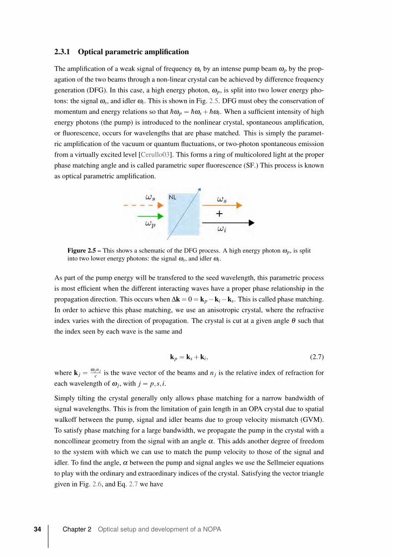
2.3.1 Optical parametric amplification
The amplification of a weak signal of frequency ωs by an intense pump beam ωp by the prop-
agation of the two beams through a non-linear crystal can be achieved by difference frequency
generation (DFG). In this case, a high energy photon, ωp, is split into two lower energy pho-
tons: the signal ωs, and idler ωi. This is shown in Fig. 2.5. DFG must obey the conservation of
momentum and energy relations so that hωp “ hωs` hωi. When a sufficient intensity of high
energy photons (the pump) is introduced to the nonlinear crystal, spontaneous amplification,
or fluorescence, occurs for wavelengths that are phase matched. This is simply the paramet-
ric amplification of the vacuum or quantum fluctuations, or two-photon spontaneous emission
from a virtually excited level [Cerullo03]. This forms a ring of multicolored light at the proper
phase matching angle and is called parametric super fluorescence (SF.) This process is known
as optical parametric amplification.
Figure 2.5 – This shows a schematic of the DFG process. A high energy photon ωp, is split
into two lower energy photons: the signal ωs, and idler ωi.
As part of the pump energy will be transfered to the seed wavelength, this parametric process
is most efficient when the different interacting waves have a proper phase relationship in the
propagation direction. This occurs when Δk“ 0“ kp´ki´ks. This is called phase matching.
In order to achieve this phase matching, we use an anisotropic crystal, where the refractive
index varies with the direction of propagation. The crystal is cut at a given angle θ such that
the index seen by each wave is the same and
kp “ ks`ki, (2.7)
where k j “ ω jn jc is the wave vector of the beams and n j is the relative index of refraction for
each wavelength of ω j, with j “ p,s, i.
Simply tilting the crystal generally only allows phase matching for a narrow bandwidth of
signal wavelengths. This is from the limitation of gain length in an OPA crystal due to spatial
walkoff between the pump, signal and idler beams due to group velocity mismatch (GVM).
To satisfy phase matching for a large bandwidth, we propagate the pump in the crystal with a
noncollinear geometry from the signal with an angle α . This adds another degree of freedom
to the system with which we can use to match the pump velocity to those of the signal and
idler. To find the angle, α between the pump and signal angles we use the Sellmeier equations
to play with the ordinary and extraordinary indices of the crystal. Satisfying the vector triangle
given in Fig. 2.6, and Eq. 2.7 we have
34 Chapter 2 Optical setup and development of a NOPA

����������
Figure 2.6 – Vector schematic of the 3 wave difference frequency mixing in a non-linear
material. α is the angle between the pump and signal beams and θ is the angle between the
pump and optical axis of the material. The phase matching is satisfied such that kp “ ki`ks.
|ki|2 “ |ks|2`|kp|2´2|kp||ks|cospαq . (2.8)
Since k j is the wave vector, we know
pniωiq2 “ pnsωsq2`pnpωpq2´2npωpnsωscospαq . (2.9)
This forms a solvable second order equation for np, given by
n2p´2npns
ωs
ωpcospαq` pnsωsq2´pnpωpq2
ω2p
“ 0. (2.10)
We choose a solution for the extremes of the ordinary and extraordinary indices for the crystal
for the pump, npo, npe. These are given by the ellipsoid index which depends on the angle of
the crystal,
1
np pθq “sin2 pθq
n2pe
` cos2 pθqn2
pe(2.11)
The ordinary and extraordinary indices are given by the Sellmeier equations. This allows us
to solve for θ as a function of α and ωs, the signal wavelength.
We consider our particular case using the second harmonic of our 1030 nm fiber laser at
515 nm. The amplification will be produced in the near-infrared regime. In order to shorten
the pulse and study wavelength and repetition rate dependencies, the first step is to center the
output wavelength at 800 nm in order to compare the results with those from the oscillator
and regen interactions. Plotting the phase matching dependencies for various α , we find that
the broadest bandwidth around 800 nm is found for α “ 2.6˝, typically „150 nm, as seen in
Fig. 2.7.
The biggest difficulty then becomes how to shorten the pulse and ensure the shot-to-shot sta-
bility of the NOPA output as the repetition rate changes. The NOPA output beam quality must
not change in pulse energy, duration nor profile for different repetition rates.
Section 2.3 Noncollinear Optical Parametric Amplifier (NOPA) 35
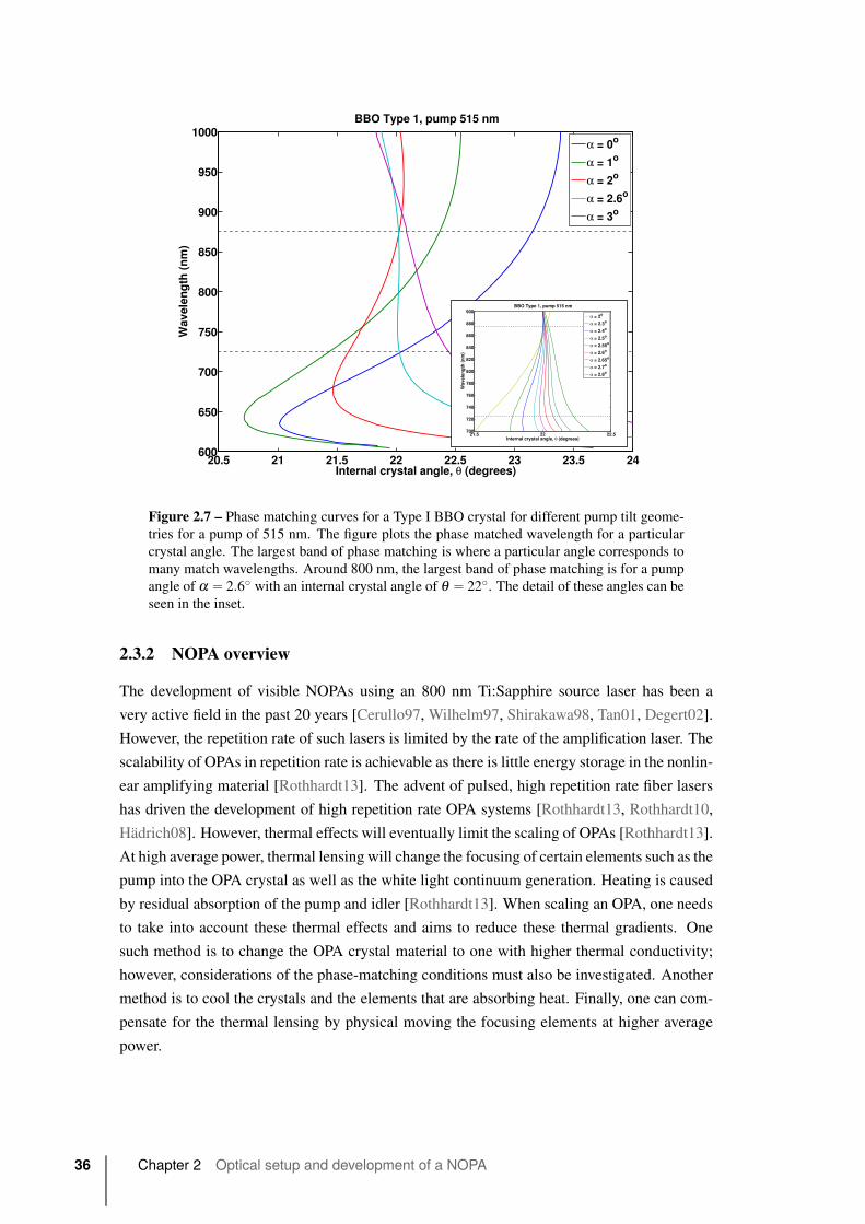
20.5 21 21.5 22 22.5 23 23.5 24600
650
700
750
800
850
900
950
1000
Internal crystal angle, θ (degrees)
Wavele
ng
th(n
m)
BBO Type 1, pump 515 nm
α = 0o
α = 1o
α = 2o
α = 2.6o
α = 3o
21.5 22 22.5700
720
740
760
780
800
820
840
860
880
900
Internal crystal angle, θ (degrees)
Wavele
ng
th(n
m)
BBO Type 1, pump 515 nm
α = 2o
α = 2.3o
α = 2.4o
α = 2.5o
α = 2.55o
α = 2.6o
α = 2.65o
α = 2.7o
α = 2.8o
Figure 2.7 – Phase matching curves for a Type I BBO crystal for different pump tilt geome-
tries for a pump of 515 nm. The figure plots the phase matched wavelength for a particular
crystal angle. The largest band of phase matching is where a particular angle corresponds to
many match wavelengths. Around 800 nm, the largest band of phase matching is for a pump
angle of α “ 2.6˝ with an internal crystal angle of θ “ 22˝. The detail of these angles can be
seen in the inset.
2.3.2 NOPA overview
The development of visible NOPAs using an 800 nm Ti:Sapphire source laser has been a
very active field in the past 20 years [Cerullo97, Wilhelm97, Shirakawa98, Tan01, Degert02].
However, the repetition rate of such lasers is limited by the rate of the amplification laser. The
scalability of OPAs in repetition rate is achievable as there is little energy storage in the nonlin-
ear amplifying material [Rothhardt13]. The advent of pulsed, high repetition rate fiber lasers
has driven the development of high repetition rate OPA systems [Rothhardt13, Rothhardt10,
Hädrich08]. However, thermal effects will eventually limit the scaling of OPAs [Rothhardt13].
At high average power, thermal lensing will change the focusing of certain elements such as the
pump into the OPA crystal as well as the white light continuum generation. Heating is caused
by residual absorption of the pump and idler [Rothhardt13]. When scaling an OPA, one needs
to take into account these thermal effects and aims to reduce these thermal gradients. One
such method is to change the OPA crystal material to one with higher thermal conductivity;
however, considerations of the phase-matching conditions must also be investigated. Another
method is to cool the crystals and the elements that are absorbing heat. Finally, one can com-
pensate for the thermal lensing by physical moving the focusing elements at higher average
power.
36 Chapter 2 Optical setup and development of a NOPA
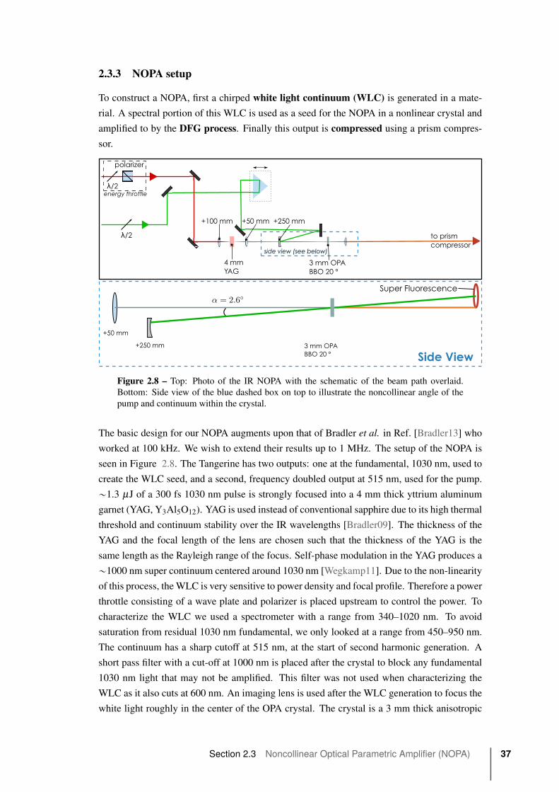
2.3.3 NOPA setup
To construct a NOPA, first a chirped white light continuum (WLC) is generated in a mate-
rial. A spectral portion of this WLC is used as a seed for the NOPA in a nonlinear crystal and
amplified to by the DFG process. Finally this output is compressed using a prism compres-
sor.
�������
������ ������
���
������
�������������
���
� ���� �������������
������� �������������
��������
�����������������
����������������
���������
�����
������ �����������������
Figure 2.8 – Top: Photo of the IR NOPA with the schematic of the beam path overlaid.
Bottom: Side view of the blue dashed box on top to illustrate the noncollinear angle of the
pump and continuum within the crystal.
The basic design for our NOPA augments upon that of Bradler et al. in Ref. [Bradler13] who
worked at 100 kHz. We wish to extend their results up to 1 MHz. The setup of the NOPA is
seen in Figure 2.8. The Tangerine has two outputs: one at the fundamental, 1030 nm, used to
create the WLC seed, and a second, frequency doubled output at 515 nm, used for the pump.
„1.3 μJ of a 300 fs 1030 nm pulse is strongly focused into a 4 mm thick yttrium aluminum
garnet (YAG, Y3Al5O12). YAG is used instead of conventional sapphire due to its high thermal
threshold and continuum stability over the IR wavelengths [Bradler09]. The thickness of the
YAG and the focal length of the lens are chosen such that the thickness of the YAG is the
same length as the Rayleigh range of the focus. Self-phase modulation in the YAG produces a
„1000 nm super continuum centered around 1030 nm [Wegkamp11]. Due to the non-linearity
of this process, theWLC is very sensitive to power density and focal profile. Therefore a power
throttle consisting of a wave plate and polarizer is placed upstream to control the power. To
characterize the WLC we used a spectrometer with a range from 340–1020 nm. To avoid
saturation from residual 1030 nm fundamental, we only looked at a range from 450–950 nm.
The continuum has a sharp cutoff at 515 nm, at the start of second harmonic generation. A
short pass filter with a cut-off at 1000 nm is placed after the crystal to block any fundamental
1030 nm light that may not be amplified. This filter was not used when characterizing the
WLC as it also cuts at 600 nm. An imaging lens is used after the WLC generation to focus the
white light roughly in the center of the OPA crystal. The crystal is a 3 mm thick anisotropic
Section 2.3 Noncollinear Optical Parametric Amplifier (NOPA) 37
crystal β -barium borate (BBO) cut with an angle of θ “ 20˝ and used at θ “ 22˝. A thick
crystal is chosen to help alleviate thermal effects and optimized for conversion efficiency and
bandwidth [Bradler13].
Since the laser has a frequency doubling stage, this step is not incorporated into the NOPA
setup. The time delay between the 515 nm pump and the chirped WLC determines what
wavelength will be amplified as the signal because the WLC is strongly chirped during its
generation. The pump light is then tilted upwards and focused using a spherical curved mirror
with a focal length of +250 mm to focus slightly after the OPA crystal. The pump arrives in the
crystal with an internal angle of α “ 2.6˝ for optimum phase matching conditions as seen in
Fig. 2.7. The crystal is tilted such that the angle between signal and optical axis is 22˝ to allow
phase matching between the signal and idler for a bandwidth of „150 nm as explained above
and in Fig. 2.7. This angle is generally set by looking at the SF ring produced by the unseeded
pump beam propagating in the crystal. In a visible NOPA, this looks like a multicolored ring
whose width changes with respect to the crystal angle. The angle is correct when the ring
width is minimized and all the colors arrive at the same place. As our NOPA amplifies in the
IR, this ring is not visible to the naked eye, making it very tricky to set. The SF ring therefore
must be observed using an IR viewer. The angle is set by minimizing the width of the ring as
seen in the viewer and comparing that to the calculated angle.
As the WLC is heavily chirped, and the pump duration is „300 fs, the output of the NOPA
will be very long temporally, on the order of „300 fs as well. The pulses can be compressed
with a prism compressor. The derivation and physics behind these compressors can be found
in the seminal paper by Fork, et al. in Ref. [Fork84].
Preliminary results are presented in the next section.
2.3.4 Characterization of the NOPA output
In this section, I present various figures and plots showing the characterization of the NOPA
pulses. As one of the key features of a NOPA is the possibility to tune the wavelength by
amplifying different portions of the signal white light continuum, while varying the repetition
rate, this means that the beam quality must remain relatively uniform over these changing
conditions. This NOPA is still under development at the time of the writing of this manuscript.
Presented here are preliminary results.
WLC characterization:Fig. 2.9 shows the white light continuum generated for different repetition rates, with an input
energy of „1.3 μJ per pulse into the YAG. The spectral intensity has been normalized to ac-
count for the different repetition rates over the integration time. The input energy was chosen
such that the continuum shape remained stable from shot-to-shot as well as over long peri-
ods time. At higher energies, multiple filamentation begins to occur in the YAG and spectral
fringes and instabilities begin to appear in the spectra. At lower energies, thermal effect over-
take the continuum generation and suppress the broadening of the spectra between 600 and
800 nm. The continuum remains stable in shape in the 550–850 nm bandwidth up between
38 Chapter 2 Optical setup and development of a NOPA
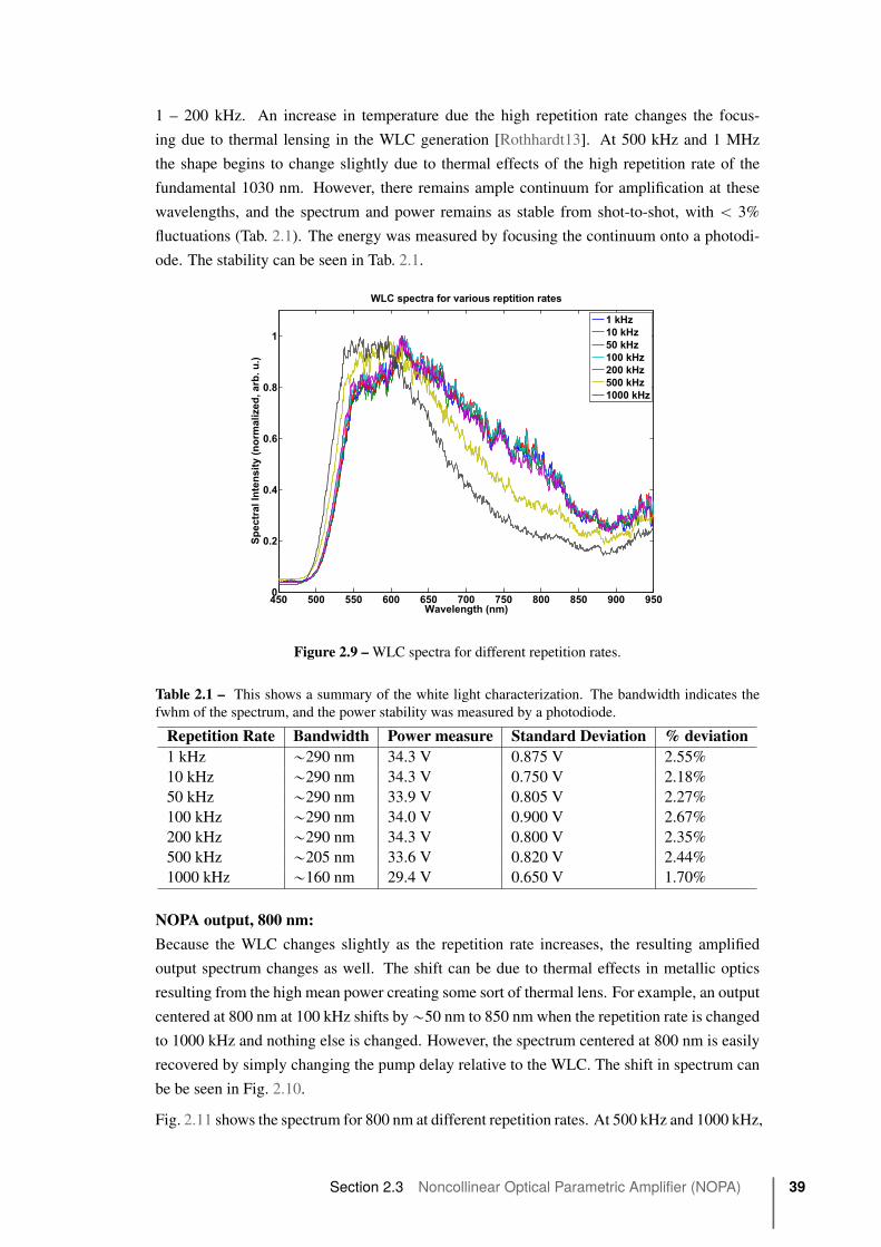
1 – 200 kHz. An increase in temperature due the high repetition rate changes the focus-
ing due to thermal lensing in the WLC generation [Rothhardt13]. At 500 kHz and 1 MHz
the shape begins to change slightly due to thermal effects of the high repetition rate of the
fundamental 1030 nm. However, there remains ample continuum for amplification at these
wavelengths, and the spectrum and power remains as stable from shot-to-shot, with ă 3%
fluctuations (Tab. 2.1). The energy was measured by focusing the continuum onto a photodi-
ode. The stability can be seen in Tab. 2.1.
450 500 550 600 650 700 750 800 850 900 9500
0.2
0.4
0.6
0.8
1
Wavelength (nm)
Spec
tral
Inte
nsity
(nor
mal
ized
, arb
. u.)
WLC spectra for various reptition rates
1 kHz10 kHz50 kHz100 kHz200 kHz500 kHz1000 kHz
Figure 2.9 – WLC spectra for different repetition rates.
Table 2.1 – This shows a summary of the white light characterization. The bandwidth indicates the
fwhm of the spectrum, and the power stability was measured by a photodiode.
Repetition Rate Bandwidth Power measure Standard Deviation % deviation1 kHz „290 nm 34.3 V 0.875 V 2.55%
10 kHz „290 nm 34.3 V 0.750 V 2.18%
50 kHz „290 nm 33.9 V 0.805 V 2.27%
100 kHz „290 nm 34.0 V 0.900 V 2.67%
200 kHz „290 nm 34.3 V 0.800 V 2.35%
500 kHz „205 nm 33.6 V 0.820 V 2.44%
1000 kHz „160 nm 29.4 V 0.650 V 1.70%
NOPA output, 800 nm:Because the WLC changes slightly as the repetition rate increases, the resulting amplified
output spectrum changes as well. The shift can be due to thermal effects in metallic optics
resulting from the high mean power creating some sort of thermal lens. For example, an output
centered at 800 nm at 100 kHz shifts by„50 nm to 850 nm when the repetition rate is changed
to 1000 kHz and nothing else is changed. However, the spectrum centered at 800 nm is easily
recovered by simply changing the pump delay relative to the WLC. The shift in spectrum can
be be seen in Fig. 2.10.
Fig. 2.11 shows the spectrum for 800 nm at different repetition rates. At 500 kHz and 1000 kHz,
Section 2.3 Noncollinear Optical Parametric Amplifier (NOPA) 39
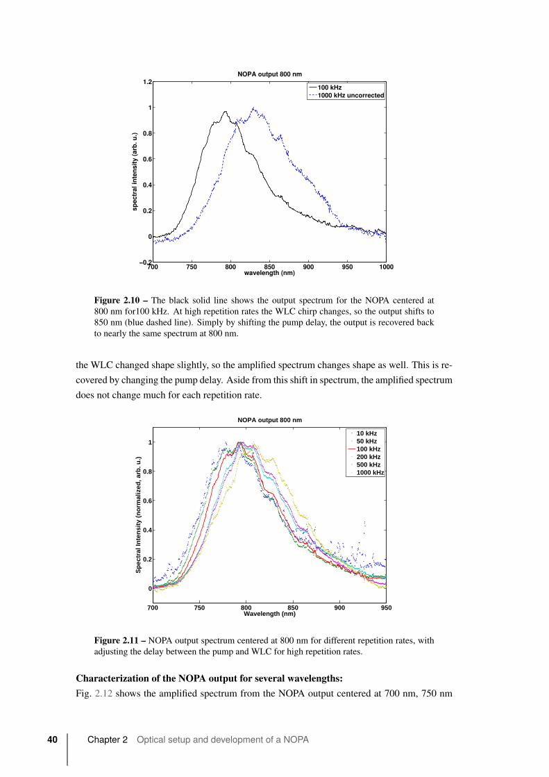
700 750 800 850 900 950 1000−0.2
0
0.2
0.4
0.6
0.8
1
1.2
wavelength (nm)
spec
tral
inte
nsi
ty (
arb
. u.)
NOPA output 800 nm
100 kHz1000 kHz uncorrected
Figure 2.10 – The black solid line shows the output spectrum for the NOPA centered at
800 nm for100 kHz. At high repetition rates the WLC chirp changes, so the output shifts to
850 nm (blue dashed line). Simply by shifting the pump delay, the output is recovered back
to nearly the same spectrum at 800 nm.
the WLC changed shape slightly, so the amplified spectrum changes shape as well. This is re-
covered by changing the pump delay. Aside from this shift in spectrum, the amplified spectrum
does not change much for each repetition rate.
700 750 800 850 900 950
0
0.2
0.4
0.6
0.8
1
Wavelength (nm)
Sp
ectr
al In
ten
sity
(n
orm
aliz
ed, a
rb. u
.)
NOPA output 800 nm
10 kHz50 kHz100 kHz200 kHz500 kHz1000 kHz
Figure 2.11 – NOPA output spectrum centered at 800 nm for different repetition rates, with
adjusting the delay between the pump and WLC for high repetition rates.
Characterization of the NOPA output for several wavelengths:Fig. 2.12 shows the amplified spectrum from the NOPA output centered at 700 nm, 750 nm
40 Chapter 2 Optical setup and development of a NOPA

and 800 nm. The bandwidth of each output and corresponding Fourier limit can be found in
Tab. 2.2.
650 700 750 800 850 900 950−0.2
0
0.2
0.4
0.6
0.8
1
1.2
Wavelength (nm)
Sp
ectr
al In
ten
sity
(n
orm
aliz
ed, a
rb. u
.)
NOPA output, 100 kHz
700 nm750 nm800 nm
Figure 2.12 – Output NOPA spectra for different central wavelengths.
Table 2.2 – This shows a summary of the NOPA output spectra bandwidths and corresponding calcu-
lated Fourier limits.
Centered wavelength Bandwidth (fwhm) Fourier limit700 nm 44 nm 17 fs
750 nm 67 nm 13 fs
800 nm 84 nm 11 fs
The peak-to-peak energy stability for the NOPA output is measured with a photodiode, after a
1000 nm short pass filter to eliminate any fundamental 1030 nm which is unconverted in the
WLC generation process. Due to the efficiency of the white light generation and the phase
matching conditions (Fig. 2.7 inset), the NOPA is much brighter at 750 nm compared to the
other output wavelengths. At each repetition rate the energy fluctuation per pulse is less than
5% and generally around 2%. At high repetition rates, the efficiency begins to go down, and
the output energy of the NOPA decreases. There are possible thermal effects as the crystal also
is found to absorb heat mainly through pump absorption [Rothhardt13]. The fluctuations in
energy, however, are still on the order of 5% at these rates. This is seen in of Fig. 2.13.
Section 2.3 Noncollinear Optical Parametric Amplifier (NOPA) 41

10−1
100
101
102
103
1040
0.05
0.1
0.15
0.2
0.25
0.3
0.35
Repetition Rate (kHz)
En
erg
y/p
uls
e (μ
J)
NOPA energy/pulse for various repetition rates (before compressor)
700 nm750 nm800 nm
Figure 2.13 – NOPA energy measurements for different repetition rates at 700 nm, 750 nm
and 800 nm.
NOPA parametric gain:We investigated the parametric gain as a function of the power density of the pump for a
given repetition rate (100 kHz) to see if there are any saturation or depletion effects in the
amplification process. The 300 fs pump is focused to a spot size of „80 μm in diameter. The
crystal is placed slightly before the focus, so the spot in the crystal is on the order of „150μm
in diameter. The parametric gain remains linear and no saturation effects or depletion can be
seen (Fig. 2.14).
400 500 600 700 800 900 1000 1100 12005
10
15
20
25
30
35
40
45
50
55
515 pump power density (W cm−2)
NO
PA
po
wer
(m
W)
NOPA output conversion, 750nm, 100 kHz
Figure 2.14 – Parametric gain for different pump powers.
42 Chapter 2 Optical setup and development of a NOPA
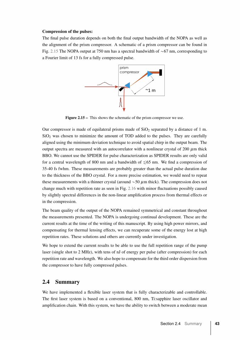
Compression of the pulses:The final pulse duration depends on both the final output bandwidth of the NOPA as well as
the alignment of the prism compressor. A schematic of a prism compressor can be found in
Fig. 2.15 The NOPA output at 750 nm has a spectral bandwidth of „67 nm, corresponding to
a Fourier limit of 13 fs for a fully compressed pulse.
�������������
���
Figure 2.15 – This shows the schematic of the prism compressor we use.
Our compressor is made of equilateral prisms made of SiO2 separated by a distance of 1 m.
SiO2 was chosen to minimize the amount of TOD added to the pulses. They are carefully
aligned using the minimum deviation technique to avoid spatial chirp in the output beam. The
output spectra are measured with an autocorrelator with a nonlinear crystal of 200 μm thick
BBO. We cannot use the SPIDER for pulse characterization as SPIDER results are only valid
for a central wavelength of 800 nm and a bandwidth of À65 nm. We find a compression of
35-40 fs fwhm. These measurements are probably greater than the actual pulse duration due
to the thickness of the BBO crystal. For a more precise estimation, we would need to repeat
these measurements with a thinner crystal (around „50 μm thick). The compression does not
change much with repetition rate as seen in Fig. 2.16 with minor fluctuations possibly caused
by slightly spectral differences in the non-linear amplification process from thermal effects or
in the compression.
The beam quality of the output of the NOPA remained symmetrical and constant throughout
the measurements presented. The NOPA is undergoing continual development. These are the
current results at the time of the writing of this manuscript. By using high power mirrors, and
compensating for thermal lensing effects, we can recuperate some of the energy lost at high
repetition rates. These solutions and others are currently under investigation.
We hope to extend the current results to be able to use the full repetition range of the pump
laser (single shot to 2 MHz), with tens of nJ of energy per pulse (after compression) for each
repetition rate and wavelength. We also hope to compensate for the third order dispersion from
the compressor to have fully compressed pulses.
2.4 Summary
We have implemented a flexible laser system that is fully characterizable and controllable.
The first laser system is based on a conventional, 800 nm, Ti:sapphire laser oscillator and
amplification chain. With this system, we have the ability to switch between a moderate mean
Section 2.4 Summary 43
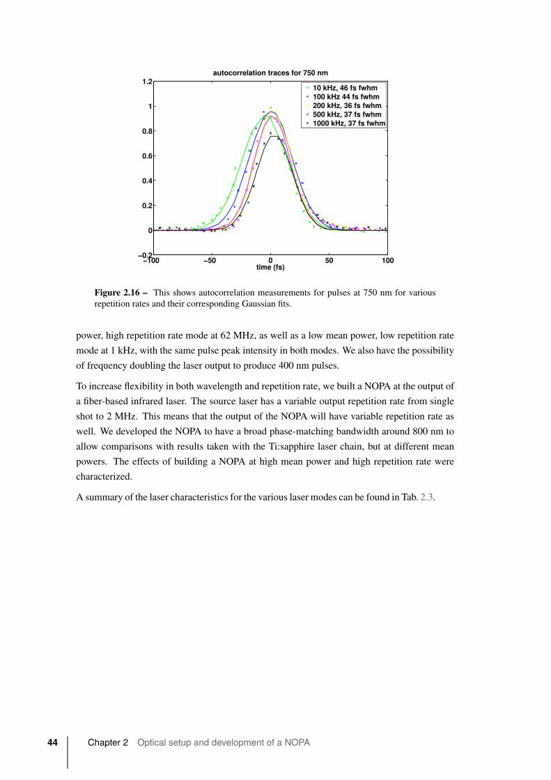
−100 −50 0 50 100−0.2
0
0.2
0.4
0.6
0.8
1
1.2
time (fs)
autocorrelation traces for 750 nm
10 kHz, 46 fs fwhm100 kHz 44 fs fwhm200 kHz, 36 fs fwhm500 kHz, 37 fs fwhm1000 kHz, 37 fs fwhm
Figure 2.16 – This shows autocorrelation measurements for pulses at 750 nm for various
repetition rates and their corresponding Gaussian fits.
power, high repetition rate mode at 62 MHz, as well as a low mean power, low repetition rate
mode at 1 kHz, with the same pulse peak intensity in both modes. We also have the possibility
of frequency doubling the laser output to produce 400 nm pulses.
To increase flexibility in both wavelength and repetition rate, we built a NOPA at the output of
a fiber-based infrared laser. The source laser has a variable output repetition rate from single
shot to 2 MHz. This means that the output of the NOPA will have variable repetition rate as
well. We developed the NOPA to have a broad phase-matching bandwidth around 800 nm to
allow comparisons with results taken with the Ti:sapphire laser chain, but at different mean
powers. The effects of building a NOPA at high mean power and high repetition rate were
characterized.
A summary of the laser characteristics for the various laser modes can be found in Tab. 2.3.
44 Chapter 2 Optical setup and development of a NOPA
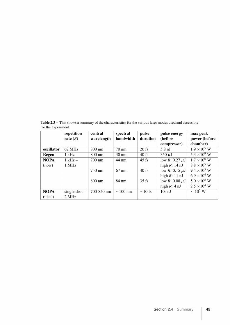
Table 2.3 – This shows a summary of the characteristics for the various laser modes used and accessible
for the experiment.
repetition central spectral pulse pulse energy max peakrate (R) wavelength bandwidth duration (before power (before
compressor) chamber)oscillator 62 MHz 800 nm 70 nm 20 fs 5.8 nJ 1.9 ˆ105 W
Regen 1 kHz 800 nm 30 nm 40 fs 350 μJ 5.3 ˆ109 W
NOPA 1 kHz – 700 nm 44 nm 45 fs low R: 0.27 μJ 1.7 ˆ106 W
(now) 1 MHz high R: 14 nJ 8.8 ˆ105 W
750 nm 67 nm 40 fs low R: 0.15 μJ 9.4 ˆ105 W
high R: 11 nJ 6.9 ˆ104 W
800 nm 84 nm 35 fs low R: 0.08 μJ 5.0 ˆ105 W
high R: 4 nJ 2.5 ˆ104 W
NOPA single shot – 700-850 nm „100 nm „10 fs 10s nJ „ 105 W
(ideal) 2 MHz
Section 2.4 Summary 45


3Experimental setup and methods
This chapter describes the experimental setup used for my thesis research (Fig. 3.1). This
setup was developed entirely during my Ph.D. research. Prior to my arrival, my group was
involved in laser development for coherent control techniques. The aim of my thesis was able
to combine their laser expertise with a new experimental setup to investigate the light-matter
interaction at a sharp nanotip. As this is a brand new scientific direction for the group, the ex-
perimental setup went through much evolution during my Ph.D. with this group. In general, the
setup is very versatile, involving many different elements from laser development to electron
detection as well as vacuum technologies and home made data acquisition software.
For my Ph.D. research, I used 3 kinds of nanotips: tungsten nanotips which I made myself
at CEMES; carbon cones which were made at CEMES by Aurélien Masseboeuf; and silver
nanotips which were made by Ivan Blum at GPM in Rouen. I will first discuss the sample
making procedure for the various nanotips we use. I will then discuss the experimental cham-
ber, sample manipulators and detectors. Finally, I will discuss the alignment procedure for the
various elements.
����������
�� � � ����������
�������������
Figure 3.1 – This shows the basic flow of the experiment. A sharp nanotip placed in a vacuum
chamber is illuminated by a laser source. The resulting electron emission is then detected by
an electron spectrometer.
As shown in Fig. 3.1, the nanotip is placed in an ultra-high vacuum (UHV) chamber and
illuminated by a tightly focused ultrafast laser source as described in Chap. 2. The emitted
electrons are then detected with a field retarding electron spectrometer, with the possibility of
spatially resolved detection.

3.1 Nanotip fabrication and characterization
Tungsten tips were first used as a benchmark tip to compare results from our new setup to
established experiments and identify various emission mechanisms. We then investigate emis-
sion from novel new nanotips based on a single carbon nanotube and from silver.
3.1.1 Tungsten tips
Emission from tungsten nanotips were the first results investigated during my Ph.D. Their
emission patterns provide a baseline for results with our new experimental setup that we can
compare to other established experiments [Hommelhoff06b, Schenk10, Barwick07, Hommelhoff06a,
Yanagisawa10]. Tungsten (W, atomic number 74) provides a robust material to study with its
high melting point, 3695 K, and a work function of „4.5 eV. The high melting point makes
tungsten tips ideal for field emission and microscopy. Tip formation methods via electro-
chemical etching are well known [Lucier04, Tsong90, Ekvall99].
The tips are made via electrochemical etching. As LCAR is not an electron microscopy labo-
ratory, we turned to our collaboration with Aurélien Masseboeuf and the Nanomaterials group
at the Centre d’Élaboration de Matériaux et d’Etudes Structurales (CEMES)1 laboratory in
Toulouse, France. This method of tip making is the most basic of creation of sharp nanotips.
In electrochemical etching of sharp nanotips, a small diameter metal wire is dipped in an elec-
trolyte solution. A small voltage is applied between the wire and the electrolyte until enough
dissolution occurs that the wire has a sharp tip.
����������
� �������� ����
�� ���������������
�� ���������� �����
���
���������
Figure 3.2 – This shows schematic of tip. A tungsten filament is welded onto metal plugs
with a ceramic support. A straight tungsten wire is welded to this filament onto which the
nanotip is electro-chemically etched. SEM images of the welded junctions (dashed boxes)
can be seen in Fig. 3.3
The tip base is a FEI and Philips2 Standard V Loop Filament. This base consists of a ceramic
disk, 26 mm in diameter, that is cut in half. The disk is cut in half to allow the base to fit in a
1 http://www.cemes.fr/2 http://www.fei.com/
48 Chapter 3 Experimental setup and methods

Focused Ion Beam (FIB) environment for the eventual case of attaching a carbon cone to the
end of the tungsten tip (see Sec. 3.1.2).
Usually the filament base for the tip is made from polycrystalline tungsten wire, and the tip
is etched from single crystal tungsten oriented along the (310) direction. This means that the
apex of the tip created will be oriented along the (310) axis. W(310) was chosen because it has
the lowest work function, 4.35 eV [Mendenhall37], of all possible orientations and therefore
is the brightest emitter [Yanagisawa09].
Since the bases are reused to make new tips, the first step to tip making is to make the filament.
Tungsten wire 0.125 mm in diameter is bent into a ‘V’ shape, approximately„3 mm deep and
the ends of the ‘V’ are the same distance apart as the plugs in the ceramic disk (5 mm). The
filament is micro-welded on either end to the plugs of the tip base. The micro-welder is set
to short current and 2 Ws and works by sending a short burst of current through the wires to
be welded together. A small length of tungsten wire, „3-4 mm long, is welded to the point of
the filament. This wire is to be etched into a tip. The height of the wire should be 9-11 mm
from the top of the ceramic plate. Since the etching process shortens the wire by 1 mm, this
corresponds to a final height of 8-10 mm from the top of the plate. A schematic of the tip base
can be seen in Fig. 3.2 with SEM images of the welds seen in Fig. 3.3.
(a) (b)
Figure 3.3 – This shows SEM images of the micro-weld of a filament to the ceramic tip base
plugs. (a) This is a typical weld between the filament and a plug. (b) This is a typical weld
between a filament and the to-be-etched tip wire.
The actual tip is formed via electrochemical etching in a 2 M NaOH solution. The electro-
chemical attack is performed by sending a voltage through the wire to be etched and the solu-
tion. The wire acts as the anode and is attached to the positive end of the voltage supplier, and
the solution itself is used as the cathode and is connected to the negative end. The wire is then
dipped 1.0 mm into the solution and lifted up 0.1 mm to form a meniscus. Due to the surface
tension of the NaOH solution, a dip in surface of the solution is apparent when the wire enters
the solution. An attack voltage of 4.2 V is applied to the tip with a base voltage of 0.5 V. A
schematic of the setup is seen in Fig. 3.4.
The overall reaction [Ibe90] that occurs during the electrochemical etching process is given
Section 3.1 Nanotip fabrication and characterization 49

���
���������� ����
������� ����
���������
Figure 3.4 – This shows the setup developed at CEMES for electrochemical etching of the
W tips. Adapted from [Bedel14].
by:
cathode : 6H2O`6e´Ñ 3H2pgq`6OH´
anode : W psq`8OH´ÑWO2´4 `4H2O`6e´
W psq`2OH´`2H2OÑWO2´4 `3H2pgq
As the etching occurs at the air/electrolyte interface, the shape of the meniscus is especially
important in determining the tip shape. Due to a concentration gradient of OH´ along the
axis of the tip, the etching rate is higher at the top of the meniscus. During the tip formation,
the soluble tungsten flows towards the lower end of the wire forming a necking phenomenon
which is observed at the meniscus interface. More details on the etching process can be found
in [Ibe90, Lucier04, Bedel14].
(a) (b)
Figure 3.5 – (a) This shows SEM images of the final etched tungsten tip. Note the residual
salt pollution leftover from the etching process. These are removed via current flash cleaning.
(b) 10,000x magnification of the tip apex with 85,000x magnification in the inset.
As the neck of the wire becomes thinner, at some point the weight of the lower part of the wire
is too much and the neck cannot support it. The lower part of the wire then breaks off forming
the sharp tip. Afterwards the voltage must be immediately shut off as the etching process does
not stop just because a tip has been formed. A circuit monitoring the current between the
cathode and the anode provides the mechanism for shutting of the voltage quickly after the
tip has been formed. The circuit design is based on that of Nakamura et al. [Nakamura99]
50 Chapter 3 Experimental setup and methods
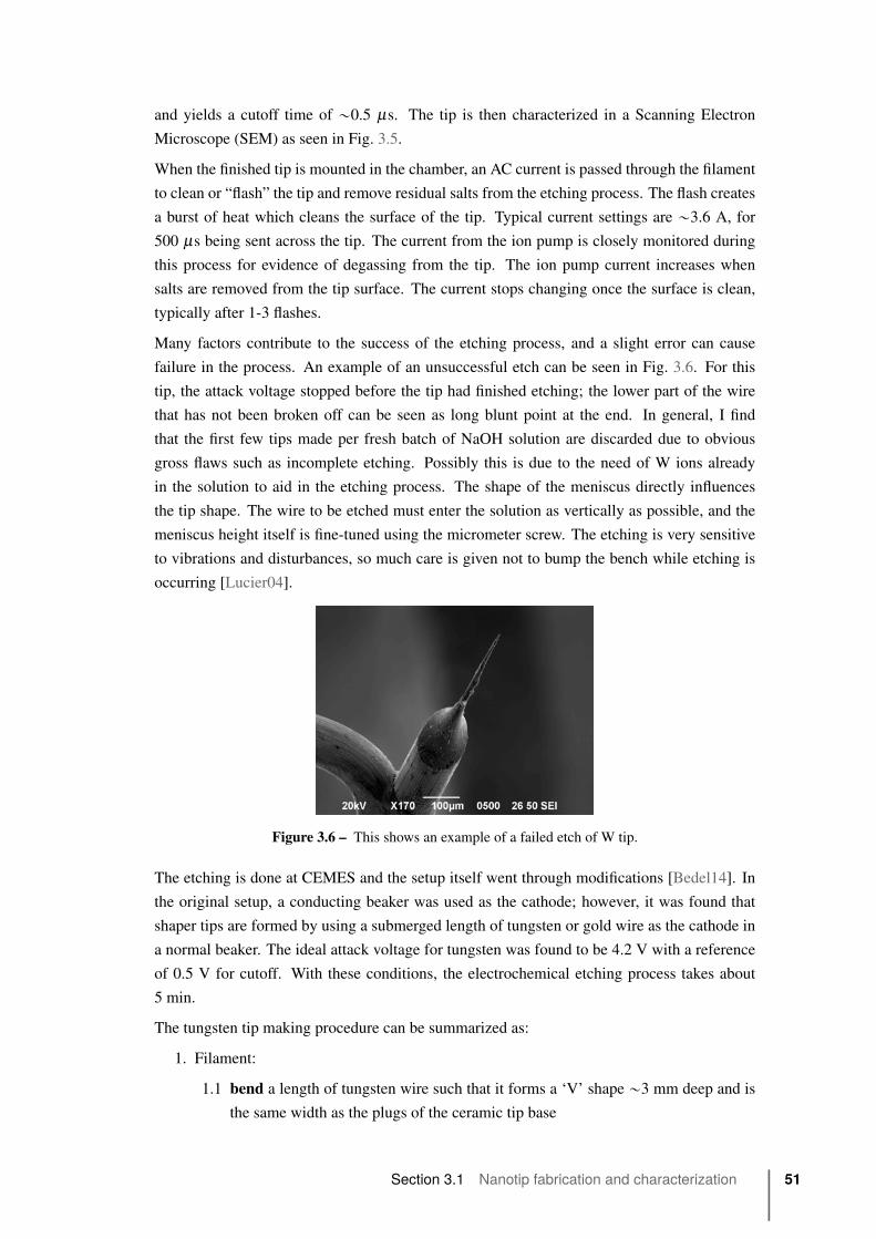
and yields a cutoff time of „0.5 μs. The tip is then characterized in a Scanning Electron
Microscope (SEM) as seen in Fig. 3.5.
When the finished tip is mounted in the chamber, an AC current is passed through the filament
to clean or “flash” the tip and remove residual salts from the etching process. The flash creates
a burst of heat which cleans the surface of the tip. Typical current settings are „3.6 A, for
500 μs being sent across the tip. The current from the ion pump is closely monitored during
this process for evidence of degassing from the tip. The ion pump current increases when
salts are removed from the tip surface. The current stops changing once the surface is clean,
typically after 1-3 flashes.
Many factors contribute to the success of the etching process, and a slight error can cause
failure in the process. An example of an unsuccessful etch can be seen in Fig. 3.6. For this
tip, the attack voltage stopped before the tip had finished etching; the lower part of the wire
that has not been broken off can be seen as long blunt point at the end. In general, I find
that the first few tips made per fresh batch of NaOH solution are discarded due to obvious
gross flaws such as incomplete etching. Possibly this is due to the need of W ions already
in the solution to aid in the etching process. The shape of the meniscus directly influences
the tip shape. The wire to be etched must enter the solution as vertically as possible, and the
meniscus height itself is fine-tuned using the micrometer screw. The etching is very sensitive
to vibrations and disturbances, so much care is given not to bump the bench while etching is
occurring [Lucier04].
Figure 3.6 – This shows an example of a failed etch of W tip.
The etching is done at CEMES and the setup itself went through modifications [Bedel14]. In
the original setup, a conducting beaker was used as the cathode; however, it was found that
shaper tips are formed by using a submerged length of tungsten or gold wire as the cathode in
a normal beaker. The ideal attack voltage for tungsten was found to be 4.2 V with a reference
of 0.5 V for cutoff. With these conditions, the electrochemical etching process takes about
5 min.
The tungsten tip making procedure can be summarized as:
1. Filament:
1.1 bend a length of tungsten wire such that it forms a ‘V’ shape „3 mm deep and is
the same width as the plugs of the ceramic tip base
Section 3.1 Nanotip fabrication and characterization 51

1.2 micro-weld the ends of the filament to the base plugs
1.3 micro-weld a 4-5 mm length of tungsten wire to the middle of the filament
2. Etch the tip:
2.1 fill a beaker with 2 M NaOH solution
2.2 attach negative output of voltage tip attack box to a wire submerged in the solution
and the positive output to one of the base plugs
2.3 lower the base until the tungsten wire is submerge 1.0 mm into the solution
2.4 lift the base up 0.1 mm to prepare the meniscus
2.5 use the tip attack box to apply voltage and start the etching process–the box will
automatically shutoff once the process is finished
3.1.2 Carbon Cone nanoTips (CCnT)
Carbon cone nanotips (CCnT) [Jacobsen97, Houdellier12] are samples made in collaboration
with CEMES. The CCnTs are synthesized by Mathieu Delmas and are mounted entirely at
CEMES by Aurélien Masseboeuf.
Figure 3.7 – This shows two carbon cone nanotips (CCnT) formed on either end of a short
microfiber segment, which can be described as crumpled graphene sheets, that terminate
with two opposed, smooth surfaced carbon cones. Adapted from Carbon, Vol 50, F. Houdel-
lier et al., “New carbon cone nanotip for use in a highly coherent cold field emission elec-
tron microscope,” Pages No. 2037–2044, Copyright (2012), with permission from Elsevier.
[Houdellier12].
CCnTs are based on a single multiwall carbon (C, atomic number 12) nanotube surrounded
by concentric graphene sheets. The interior structure of the concentric graphene sheets can be
seen in the Transmission electron microscopy (TEM) of Fig. 3.8. The structures are formed
via a controllable time of flight chemical vapor deposition process [Allouche03, Allouche05,
Monthioux06]. This recently developed nanotip raises high expectations for advances by im-
plementation in electron microscopy [Houdellier12, Houdellier15]. The carbon cone is grown
onto a single multi-wall carbon nanotube (CNT) with an apex diameter of a few nm, and
mounted on a tungsten tip with a focused ion beam and a gas precursor injection system (FIB
induced deposition, FIBID), as shown in Fig. 3.9. The use of this CNT-based nanotip (CCnT)
has several advantages over W and Au nanotips. The mechanical and chemical strength of the
carbon sp2 bonds is larger, increasing robustness and stability. The aspect ratio of the carbon
cone is sharper and the apex size can be smaller, which can lead to a higher field enhance-
ment in the vicinity of the apex. The growth of the carbon cone can be completely controlled,
which could allow modification of the electronic structure by doping or filling the CNT with
52 Chapter 3 Experimental setup and methods

Figure 3.8 – This shows the interior structure of the concentric graphene sheets that make up
the carbon cones via transmission electron microscopy (TEM).
other elements. A collaboration with CEMES and Raul Arenal at the University of Zaragoza
is studying ways to grow CCnTs with doped CNTs. This is the research project of the Ph.D.
student Rongrong Wang. The carefully controlled growth process allows the enhancement of
properties important for cold field emission such as emission stability, life-time, and aspect
ratio. They are formed on either end of a short microfiber segment, which can be described
as crumpled graphene sheets, that terminate with two opposed, smooth surfaced carbon cones
[Jacobsen97, Houdellier12]. This is seen in Fig. 3.7. A more detailed description of a CCnT
can be found in [Houdellier12, deKnoop14].
Carbon tips are welded to the end of an already formed tungsten nanotip in a Focused Ion Beam
(FIB) environment [Houdellier12]. The sharp end of an electrochemically etched tungsten is
milled so that the end diameter is„1 μm, about the same diameter as the carbon onto which the
CCnT is attached (Fig. 3.9 (B)). A suitable CCnT is located on the substrate onto which they
have been dispersed. The CCnT must have proper alignment with the axis of the milled tip and
be free from any visible defects (Fig. 3.9 (A)). Using micro-tweezers, the CCnT is then lifted
from the substrate after being cut from its fiber base using the Ga ` ion FIB (Fig. 3.9 (C)). The
CCnT is then carefully placed in contact with the milled tungsten tip and welded into place via
W ion beam induced-deposition from W precursor (Fig. 3.9 (D)). More details on this sample
preparation process can be found in [Houdellier12] and [deKnoop14, Ch. 3].
The CCnT tip making process can be summarized as:
1. fabricate tungsten tip
2. mill the tip to end diameter of „1 μm
3. locate suitable CCnT on substrate
4. excise CCnT from carbon fiber base
5. using micro-tweezers, lift CCnT from substrate and place in contact with milled tung-
sten tip
Section 3.1 Nanotip fabrication and characterization 53

Figure 3.9 – The CCnT mounting process. (A) A suitable CCnT is chosen in alignment with
the W tip axis and with sharp apex radius (inset). (B) The tungsten tip to the approximately
the same diameter as the carbon fiber and original tip apex (inset). (C) Removal of the CCnT
from the substrate using micro-tweezers after excision from the carbon fiber (inset). (D)
The final mounted CCnT welded onto the tungsten tip. The inset shows the entire mounting
setup with the micro-tweezers on the left, the tip on the right and the gas injection nozzles
for welding on top. Reprinted from Carbon, Vol 50, F. Houdellier et al., “New carbon cone
nanotip for use in a highly coherent cold field emission electron microscope,” Pages No.
2037–2044, Copyright (2012), with permission from Elsevier. [Houdellier12]
6. weld CCnT to tungsten tip
3.1.3 Silver Tips
Experiments on silver tips are made in collaboration with the Groupe de Physique des Matéri-
aux (GPM)1 in Rouen, France. The tips are fabricated entirely at GPM.
Silver (Ag, atomic number 47) provides an interesting noble material to investigate due to its
strong plasmon resonance which in turn could yield to high electron emission and brightness.
This is due to the small imaginary component of its dielectric constant as well as low optical
damping. Generally gold is favored in air due to its inertness, but silver can be preferable in
vacuum because it is less lossy in the relevant spectral ranges [Sasaki13]. Previous studies have
demonstrated a high brightness and electron yields for silver emission an order of magnitude
more than that of tungsten [Sasaki13, Zhang11]. The work function for polycrystalline silver
is 4.26 eV [Haynes12], with a melting point of 1235 K. The melting point of silver is very low
and could lead to potential thermal issues.
1 http://gpm.labos.univ-rouen.fr/
54 Chapter 3 Experimental setup and methods
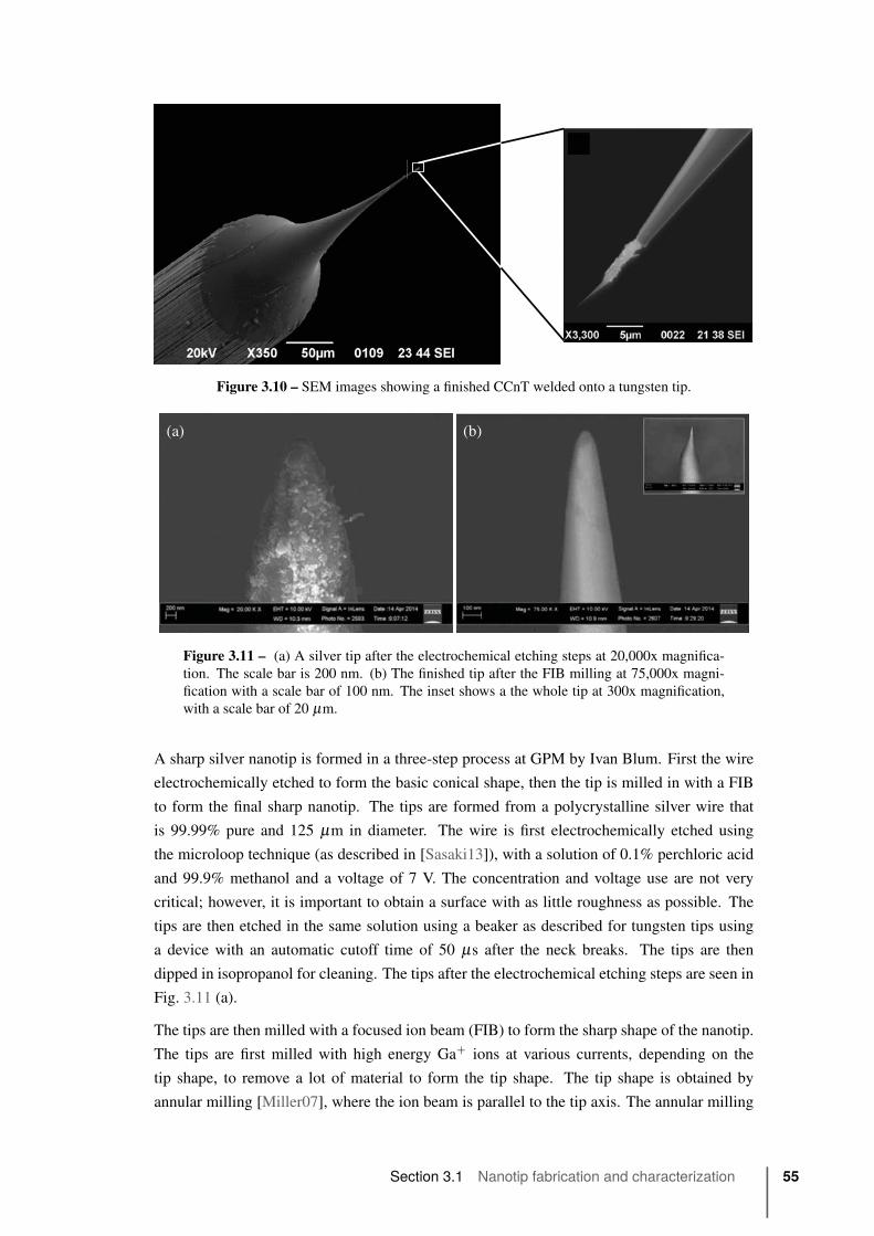
Figure 3.10 – SEM images showing a finished CCnT welded onto a tungsten tip.
(a) (b)
Figure 3.11 – (a) A silver tip after the electrochemical etching steps at 20,000x magnifica-
tion. The scale bar is 200 nm. (b) The finished tip after the FIB milling at 75,000x magni-
fication with a scale bar of 100 nm. The inset shows a the whole tip at 300x magnification,
with a scale bar of 20 μm.
A sharp silver nanotip is formed in a three-step process at GPM by Ivan Blum. First the wire
electrochemically etched to form the basic conical shape, then the tip is milled in with a FIB
to form the final sharp nanotip. The tips are formed from a polycrystalline silver wire that
is 99.99% pure and 125 μm in diameter. The wire is first electrochemically etched using
the microloop technique (as described in [Sasaki13]), with a solution of 0.1% perchloric acid
and 99.9% methanol and a voltage of 7 V. The concentration and voltage use are not very
critical; however, it is important to obtain a surface with as little roughness as possible. The
tips are then etched in the same solution using a beaker as described for tungsten tips using
a device with an automatic cutoff time of 50 μs after the neck breaks. The tips are then
dipped in isopropanol for cleaning. The tips after the electrochemical etching steps are seen in
Fig. 3.11 (a).
The tips are then milled with a focused ion beam (FIB) to form the sharp shape of the nanotip.
The tips are first milled with high energy Ga` ions at various currents, depending on the
tip shape, to remove a lot of material to form the tip shape. The tip shape is obtained by
annular milling [Miller07], where the ion beam is parallel to the tip axis. The annular milling
Section 3.1 Nanotip fabrication and characterization 55

pattern is used with gradually reducing the inner radius until the correct end curvature radius is
obtained. After the shape is formed, the tips are cleaned using low energy ions. The cleaning
step removes „50 nm of material and excises the volume of material that was damaged by
the high energy ions. In general, due to the nature of the milling process, „2 nm of Ga is
implanted under the material surface. We do not believe this small amount of Ga affects the
emission processes of the Ag. The tips have a final radius of „12-50 nm. A finished tip can
be seen in Fig. 3.11 (b).
Due to the fact that these tips are made in the facilities at GPM, the tips are mounted very dif-
ferently than those based on tungsten tips. Instead, the wire tip base is inserted into a small Ni
capillary which is 4 mm in height, with an internal diameter of 0.8 mm and external diameter
of 1 mm. This capillary can fit inside of a larger, 7 mm capillary, which is mounted directly
onto the tip holder, as described in Sec. 3.3. This means that there is only one electrical con-
nection on the tip, and therefore no possibility of cleaning via current flashing. However, due
to the nature of tip fabrication (FIB milling versus electrochemical etching) there is no need to
clean the tip in this manner as there is no contamination of the surface from the etching.
The silver tip making procedure can be summarized as:
1. Micro-loop electrochemical etchingwith a solution of 0.1% perchloric acid and 99.9%
methanol and a voltage of 7 V
2. Electrochemical etching in a beaker with same solution and using a device with an
automatic cutoff time of 50 μs after the neck breaks
3. Cleaning in isopropanol
4. High energy FIB milling to form tip shape and remove a lot of material
5. Low energy FIB milling to clean tip
3.2 Vacuum chamber
The experimental setup went through several generations. These will be described in the
following sections and then summarized at the end.
The interaction region of the experimental setup is conducted inside an ultrahigh vacuum
(UHV) in a stainless steel chamber. The chamber has a pressure on the order of„ 10´10 mbar.
Good vacuum pressure is necessary to avoid fast surface contamination on the nanotip and
prevent ionization of particles caught in the laser focus. We have found that a pressure greater
than „ 10´9 mbar is not sufficient for stable emission.
Pressure is maintained with a turbomolecular pump and an ion pump. A passive Non-Evaporable
Getter (NEG) from SAES Group1 pump assists in pumping to the final base pressure. These
are based on the principle of the absorption of molecules by a porous material. The chamber
is baked for 24 - 72 hours at a temperature of 140˝ C each time it is opened. The chamber is
1 http://www.saesgetters.com/it/products/capacitorr-pumps
56 Chapter 3 Experimental setup and methods
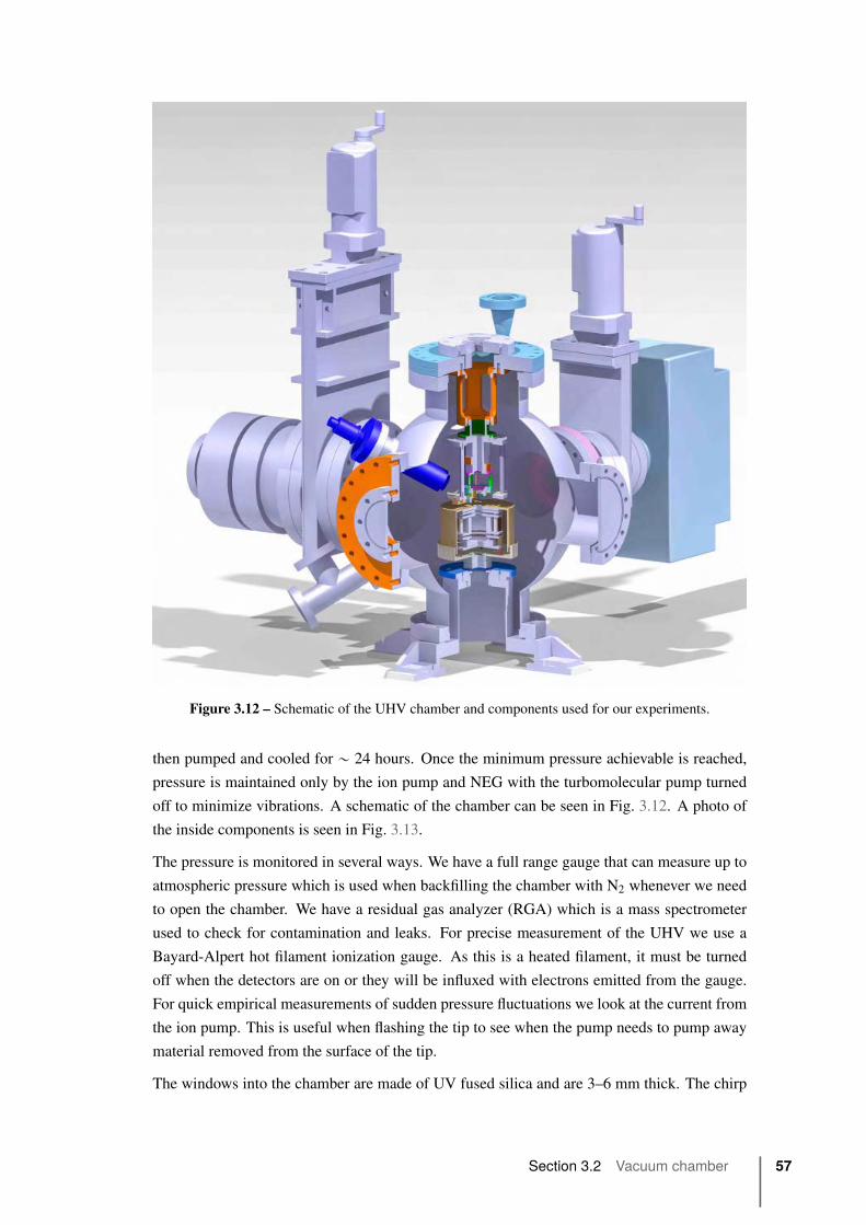
Figure 3.12 – Schematic of the UHV chamber and components used for our experiments.
then pumped and cooled for „ 24 hours. Once the minimum pressure achievable is reached,
pressure is maintained only by the ion pump and NEG with the turbomolecular pump turned
off to minimize vibrations. A schematic of the chamber can be seen in Fig. 3.12. A photo of
the inside components is seen in Fig. 3.13.
The pressure is monitored in several ways. We have a full range gauge that can measure up to
atmospheric pressure which is used when backfilling the chamber with N2 whenever we need
to open the chamber. We have a residual gas analyzer (RGA) which is a mass spectrometer
used to check for contamination and leaks. For precise measurement of the UHV we use a
Bayard-Alpert hot filament ionization gauge. As this is a heated filament, it must be turned
off when the detectors are on or they will be influxed with electrons emitted from the gauge.
For quick empirical measurements of sudden pressure fluctuations we look at the current from
the ion pump. This is useful when flashing the tip to see when the pump needs to pump away
material removed from the surface of the tip.
The windows into the chamber are made of UV fused silica and are 3–6 mm thick. The chirp
Section 3.2 Vacuum chamber 57
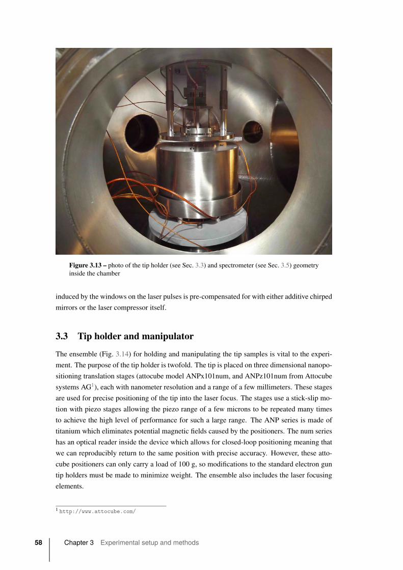
Figure 3.13 – photo of the tip holder (see Sec. 3.3) and spectrometer (see Sec. 3.5) geometry
inside the chamber
induced by the windows on the laser pulses is pre-compensated for with either additive chirped
mirrors or the laser compressor itself.
3.3 Tip holder and manipulator
The ensemble (Fig. 3.14) for holding and manipulating the tip samples is vital to the experi-
ment. The purpose of the tip holder is twofold. The tip is placed on three dimensional nanopo-
sitioning translation stages (attocube model ANPx101num, and ANPz101num from Attocube
systems AG1), each with nanometer resolution and a range of a few millimeters. These stages
are used for precise positioning of the tip into the laser focus. The stages use a stick-slip mo-
tion with piezo stages allowing the piezo range of a few microns to be repeated many times
to achieve the high level of performance for such a large range. The ANP series is made of
titanium which eliminates potential magnetic fields caused by the positioners. The num series
has an optical reader inside the device which allows for closed-loop positioning meaning that
we can reproducibly return to the same position with precise accuracy. However, these atto-
cube positioners can only carry a load of 100 g, so modifications to the standard electron gun
tip holders must be made to minimize weight. The ensemble also includes the laser focusing
elements.
1 http://www.attocube.com/
58 Chapter 3 Experimental setup and methods

Figure 3.14 – Left: A photo of the tip manipulating ensemble. Right: schematic of the
ensemble.
The tip holder is unique for each tip geometry.
3.3.1 Holder for tungsten based tips
The holder (Fig. 3.15 (a)) for tungsten based tips (single crystal W(310) and CCnT tips) pro-
vides a base for holding the tip. It is electrically separate from the rest of the setup to allow a
voltage to be applied to the tip. Most importantly it allows both plugs to be electrically con-
nected such that a current can pass through the filament, strongly heating the tip for cleaning
purposes (flash, described in Sec. 3.1.1). There is the possibility of installing an anode. The
anode is described in more detail below.
3.3.2 Holder for silver tips
The holder for silver tips (Fig. 3.15 (b)) centers the tips in the middle of the laser focus. This
holder is different than that for tungsten based tips as the silver tips are made at GPM. The tips
are electrically separated from the rest of the ensemble. A voltage can be applied to the tip.
As there is only one connection to the tip, no current can be passed through the tip. However,
due to the nature of fabrication of the silver tips, flash cleaning is not necessary.
3.3.3 Laser focus and intensity on the tip
The focusing of laser light and subsequent alignment went through several generations. In the
first setup, as seen in Fig. 3.16 (a), the laser beam is focused with an on-axis silver mirror
Section 3.3 Tip holder and manipulator 59
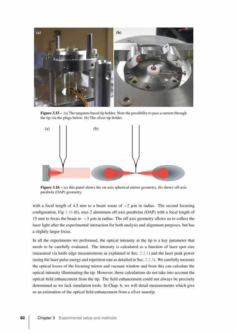
(a) (b)
Figure 3.15 – (a) The tungsten-based tip holder. Note the possibility to pass a current through
the tip via the plugs below. (b) The silver tip holder.
(a) (b)
Figure 3.16 – (a) this panel shows the on-axis spherical mirror geometry, (b) shows off-axis
parabola (OAP) geometry.
with a focal length of 4.5 mm to a beam waste of „2 μm in radius. The second focusing
configuration, Fig 3.16 (b), uses 2 aluminum off-axis parabolas (OAP) with a focal length of
15 mm to focus the beam to „3 μm in radius. The off axis geometry allows us to collect the
laser light after the experimental interaction for both analysis and alignment purposes, but has
a slightly larger focus.
In all the experiments we performed, the optical intensity at the tip is a key parameter that
needs to be carefully evaluated. The intensity is calculated as a function of laser spot size
(measured via knife edge measurements as explained in Sec. 2.2.1) and the laser peak power
(using the laser pulse energy and repetition rate as detailed in Sec. 2.2.3). We carefully measure
the optical losses of the focusing mirror and vacuum window and from this can calculate the
optical intensity illuminating the tip. However, these calculations do not take into account the
optical field enhancement from the tip. The field enhancement could not always be precisely
determined as we lack simulation tools. In Chap. 6, we will detail measurements which give
us an estimation of the optical field enhancement from a silver nanotip.
60 Chapter 3 Experimental setup and methods
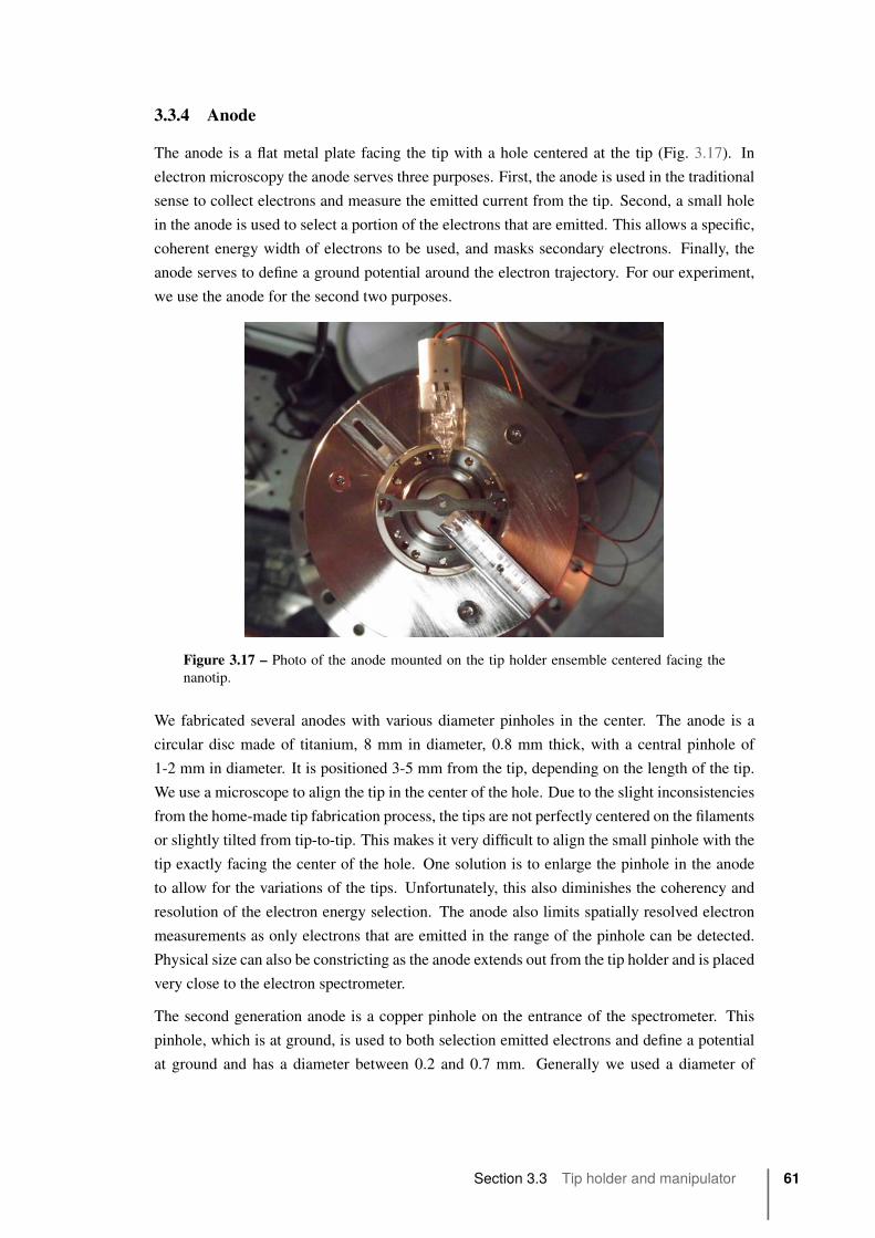
3.3.4 Anode
The anode is a flat metal plate facing the tip with a hole centered at the tip (Fig. 3.17). In
electron microscopy the anode serves three purposes. First, the anode is used in the traditional
sense to collect electrons and measure the emitted current from the tip. Second, a small hole
in the anode is used to select a portion of the electrons that are emitted. This allows a specific,
coherent energy width of electrons to be used, and masks secondary electrons. Finally, the
anode serves to define a ground potential around the electron trajectory. For our experiment,
we use the anode for the second two purposes.
Figure 3.17 – Photo of the anode mounted on the tip holder ensemble centered facing the
nanotip.
We fabricated several anodes with various diameter pinholes in the center. The anode is a
circular disc made of titanium, 8 mm in diameter, 0.8 mm thick, with a central pinhole of
1-2 mm in diameter. It is positioned 3-5 mm from the tip, depending on the length of the tip.
We use a microscope to align the tip in the center of the hole. Due to the slight inconsistencies
from the home-made tip fabrication process, the tips are not perfectly centered on the filaments
or slightly tilted from tip-to-tip. This makes it very difficult to align the small pinhole with the
tip exactly facing the center of the hole. One solution is to enlarge the pinhole in the anode
to allow for the variations of the tips. Unfortunately, this also diminishes the coherency and
resolution of the electron energy selection. The anode also limits spatially resolved electron
measurements as only electrons that are emitted in the range of the pinhole can be detected.
Physical size can also be constricting as the anode extends out from the tip holder and is placed
very close to the electron spectrometer.
The second generation anode is a copper pinhole on the entrance of the spectrometer. This
pinhole, which is at ground, is used to both selection emitted electrons and define a potential
at ground and has a diameter between 0.2 and 0.7 mm. Generally we used a diameter of
Section 3.3 Tip holder and manipulator 61

0.7 mm. Simulations performed by the Interactions Ion-Matiére (I2M)1 group at LCAR show
that the electron trajectories within the spectrometer using just the pinhole are similar to those
with the anode. Since the spectrometer is on 2D positioning stages, it can be aligned such
that the centrally emitted electrons are counted by the spectrometer. It also can be scanned to
form spatially resolved electron emission maps. More on this spectrometer functionality can
be found in Secs. 3.5 and 3.6.2.
3.3.5 Voltage applied to the tip, Vtip
We apply a negative voltage (or bias) on the tip, called -Vtip (with Vtip is always taken to be
|´Vtip| for simplicity), generally between 0 and 600 V. The tip is facing a grounded electrode:
either the grounded anode at a fixed position with respect to the tip (see Fig. 3.15), or the
entrance pinhole of the spectrometer, that is grounded by construction (see Fig. 3.18).
This creates the static electric field near the tip.
It allows two things:
• with a high Vtip (typically 300-500V), we can reach detectable cold field emission.
• with a moderate Vtip (typically 15-50V), we extract laser-induced electrons to be de-
tected by the spectrometer.
In both cases, emitted electrons reach the spectrometer with a kinetic energy equal to e¨Vtip.
3.4 Evolution of the setup
The experimental setup went through several generations.
1. In the first setup we used the anode to select electrons The laser was focused with an
on-axis spherical mirror. The spectrometer was in a fixed location with respect to the
tip. This setup was used for our tungsten results.
2. In the second setup we removed the anode and replaced it with the copper pinhole at the
entrance of the spectrometer. This alleviates some of the geometrical constraints from
the anode allowing us more flexibility with positioning the tip.
3. In the third generation of the setup, we removed the on-axis spherical mirror and re-
placed it with the OAPs (off-axis parabola). We also added nanopositioning stages un-
derneath the spectrometer allowing for 2D position. This is described below in Sec. 3.5.
3.5 Electron emission and detection: the electron spectrometer
The electron emission is collected and measured in a field retarding spectrometer [Hori75],
which gives us access to the kinetic energy distribution of the emitted electrons. Our spec-
trometer was designed and developed by the I2M group at LCAR. Electrons are detected with
1 http://www.lcar.ups-tlse.fr/spip.php?rubrique33
62 Chapter 3 Experimental setup and methods

a microchannel plate (MCP). In our measurements with an MCP, the tip is negatively bi-
ased and acts as a cathode, the electron source. The MCP ensemble1 from Hamamatsu has a
32 mm diameter active area with 2 stages. The front of the MCP is biased with +300 V, and
the backside is biased with a high voltage of +2.08 kV with a final electrode as the anode. The
field retarding spectrometer, with an entrance pinhole with a variable diameter of 0.2–0.7 mm
(usually 0.7 mm), is placed between the tip and the MCP detector. The entire spectrometer
ensemble is inside magnetic shield made of mu-metal to shield from external magnetic fields
as low velocity electrons are very sensitive to residual magnetic fields.
Figure 3.18 – left: A photo of the electron spectrometer without the magnetic shielding.
Right: schematic of the spectrometer
The spectrometer is based on a double mesh tungsten grid with an adjustable retarding field
(Vretard) combined with the MCP to record the integrated kinetic energy distribution of the
emitted electrons. The grid acts as a high-pass energy filter for the emitted electrons. Only
electrons with a minimum energy greater than that of the grid can pass and be collected. The
electron energies measured are usually referenced to the Fermi energy, which in our exper-
imental setup is equivalent to eVtip. Since the electrons that pass have little residual energy,
they are accelerated with a +30 V kick. The electrons then pass through an Einzel lens, which
redistributes the electrons over the active area of the MCP. The entrance of the MCP is at
+300 V to put the electrons which is the energy at which the MCP is most efficient. The back
is at 2.8 kV, which is the point of saturation for the gain of electron collection (corresponding
to a gain of „ 106). A schematic of the spectrometer can be found in Fig. 3.18.
1 http://www.hamamatsu.com/us/en/F2224.html
Section 3.5 Electron emission and detection: the electron spectrometer 63

���� �����
��
��
��
��
�
����� ��� ������������
���� ��� �����������
���� ��������
��������
Figure 3.19 – This shows the schematic of the MCP signal amplifier.
The signal from the MCP is passed through an decoupler, Fig 3.19, which converts the tiny
MCP signal into a signal that can be measured, a voltage of 100s of mVs. The amplified pulses
are sent through a discriminator which converts them into a transistor-transistor logic (TTL)
signal which can then be counted by the acquisition system of the computer. The discriminator
only allows hits with a certain amplitude to be counted by the computer, therefore limiting the
number of hits counted, but also lowering the noise that passes through and increasing the
signal to noise ratio.
0 5 10 1510
1
102
103
104
105
106
Energy (eV)
co
un
ts -
- lo
g s
ca
le (
arb
. u
.)
Spectrometer output(a)
0 5 10 1510
1
102
103
104
105
106
Energy (eV)
co
un
ts -
- lo
g s
ca
le (
arb
. u
.)
Unsmoothed spectrum(b)
0 5 10 1510
1
102
103
104
105
106
Energy (eV)
co
un
ts -
- lo
g s
ca
le (
arb
. u
.)
Smoothed spectrum(c)
Figure 3.20 – (a) This shows the direct output of the spectrometer, an integrated spectrum.
(b) This shows the differentiation of the output of the spectrometer, to get a kinetically re-
solved spectrum. (c) This is the spectrum after it has been smoothed with a Savitzky-Golay
distribution over 11 points.
We scan Vretard around Vtip, with steps of 0.05 V to record the electron energy spectrum. The
data collected by this type of spectrometer gives an integrated electron spectrum, Fig. 3.20 (a).
The actual electron spectrum can be retrieved by the differentiation of the recorded curve,
Fig 3.20 (b) and then smoothed with a Savitzky-Golay distribution, Fig. 3.20 (c).
This type of spectrometer has a resolution of ΔE{E „ 4 ˆ 10´3 as evaluated by simulation
from SIMION 1. This means that we must keep the applied field (E) as low as possible to
maximize resolution. By taking a static spectrum (a spectrum with a high enough Vtip to
1 simion.com
64 Chapter 3 Experimental setup and methods
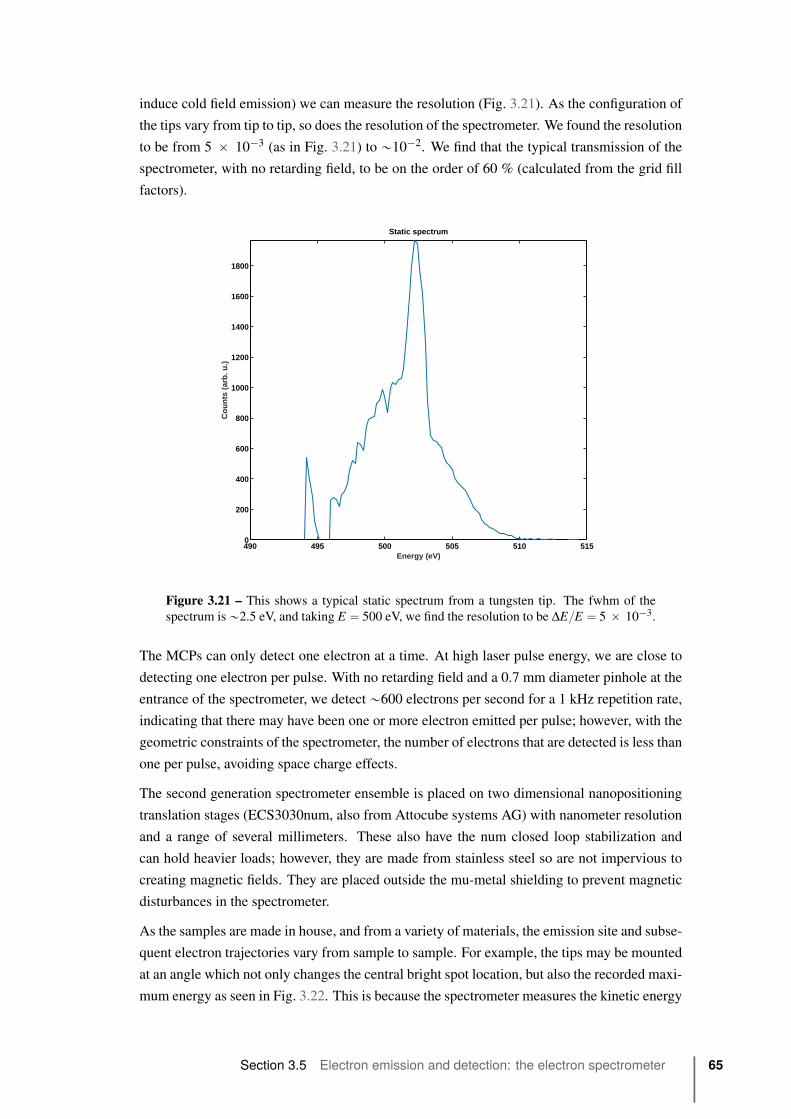
induce cold field emission) we can measure the resolution (Fig. 3.21). As the configuration of
the tips vary from tip to tip, so does the resolution of the spectrometer. We found the resolution
to be from 5 ˆ 10´3 (as in Fig. 3.21) to „10´2. We find that the typical transmission of the
spectrometer, with no retarding field, to be on the order of 60 % (calculated from the grid fill
factors).
490 495 500 505 510 5150
200
400
600
800
1000
1200
1400
1600
1800
Energy (eV)
Cou
nts
(arb
. u.)
Static spectrum
Figure 3.21 – This shows a typical static spectrum from a tungsten tip. The fwhm of the
spectrum is„2.5 eV, and taking E “ 500 eV, we find the resolution to be ΔE{E “ 5 ˆ 10´3.
The MCPs can only detect one electron at a time. At high laser pulse energy, we are close to
detecting one electron per pulse. With no retarding field and a 0.7 mm diameter pinhole at the
entrance of the spectrometer, we detect „600 electrons per second for a 1 kHz repetition rate,
indicating that there may have been one or more electron emitted per pulse; however, with the
geometric constraints of the spectrometer, the number of electrons that are detected is less than
one per pulse, avoiding space charge effects.
The second generation spectrometer ensemble is placed on two dimensional nanopositioning
translation stages (ECS3030num, also from Attocube systems AG) with nanometer resolution
and a range of several millimeters. These also have the num closed loop stabilization and
can hold heavier loads; however, they are made from stainless steel so are not impervious to
creating magnetic fields. They are placed outside the mu-metal shielding to prevent magnetic
disturbances in the spectrometer.
As the samples are made in house, and from a variety of materials, the emission site and subse-
quent electron trajectories vary from sample to sample. For example, the tips may be mounted
at an angle which not only changes the central bright spot location, but also the recorded maxi-
mum energy as seen in Fig. 3.22. This is because the spectrometer measures the kinetic energy
Section 3.5 Electron emission and detection: the electron spectrometer 65

of the electron along its axis. If the electron enters with an angle θ this means that the spec-
trometer measured and energy of Ecos2θ . The spectrometer can then be positioned centered
at the projected spot of highest electron yield, thus increasing the efficiency and resolution of
the detector.
Figure 3.22 – This shows the calculated electron energy seen by the spectrometer for an
angled tip.
The spectrometer can collect data in two ways. First the spectrometer is stationary and collects
all the electrons from one position. In general when in counting mode, the retarding field is
being scanned such that an integrated spectrum of the kinetic energy of the emitted electrons
can be recorded.
This was further developed into a second mode. This is a 2D or position scanning mode.
Here, the spectrometer can be scanned in both dimensions to study spatially resolved electron
emission. With a small pinhole on the entrance of the spectrometer (0.2-0.7 mm in diameter)
and 2D scanning, a Field Emission Microscopy (FEM)-like image is taken.
For static FEM, a high voltage is applied to the tip to induce cold field emission. The projection
of the electron trajectories (Fig. 3.23) is then recorded as a function of number of electrons
counted to the position of the spectrometer. The system works as a projection microscope with
the magnification factor given by the ratio of tip-anode distance and tip radius.
The same spatially resolved data could be taken by replacing the MCP anode with a biased
phosphor screen. The phosphor screen fluoresces when hit by an electron, and this can be
recorded by a camera. While this detection scheme allows for single-shot recording of spa-
tially resolved data, our chamber geometry and configuration does not allow for placement
of a camera so we must resort to physically moving the spectrometer for spatial data collec-
tion. Generally these phosphor screen measurements do not have as much dynamics in data
collection as our spectrometer.
66 Chapter 3 Experimental setup and methods
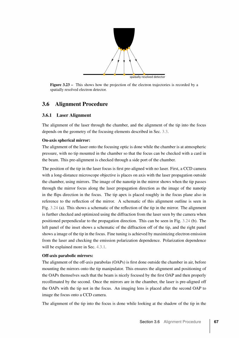
���� ��
����
����������
�������� ������ �� ��
Figure 3.23 – This shows how the projection of the electron trajectories is recorded by a
spatially resolved electron detector.
3.6 Alignment Procedure
3.6.1 Laser Alignment
The alignment of the laser through the chamber, and the alignment of the tip into the focus
depends on the geometry of the focusing elements described in Sec. 3.3.
On-axis spherical mirror:The alignment of the laser onto the focusing optic is done while the chamber is at atmospheric
pressure, with no tip mounted in the chamber so that the focus can be checked with a card in
the beam. This pre-alignment is checked through a side port of the chamber.
The position of the tip in the laser focus is first pre-aligned with no laser. First, a CCD camera
with a long-distance microscope objective is places on axis with the laser propagation outside
the chamber, using mirrors. The image of the nanotip in the mirror shows when the tip passes
through the mirror focus along the laser propagation direction as the image of the nanotip
in the flips direction in the focus. The tip apex is placed roughly in the focus plane also in
reference to the reflection of the mirror. A schematic of this alignment outline is seen in
Fig. 3.24 (a). This shows a schematic of the reflection of the tip in the mirror. The alignment
is further checked and optimized using the diffraction from the laser seen by the camera when
positioned perpendicular to the propagation direction. This can be seen in Fig. 3.24 (b). The
left panel of the inset shows a schematic of the diffraction off of the tip, and the right panel
shows a image of the tip in the focus. Fine tuning is achieved by maximizing electron emission
from the laser and checking the emission polarization dependence. Polarization dependence
will be explained more in Sec. 4.3.1.
Off-axis parabolic mirrors:The alignment of the off-axis parabolas (OAPs) is first done outside the chamber in air, before
mounting the mirrors onto the tip manipulator. This ensures the alignment and positioning of
the OAPs themselves such that the beam is nicely focused by the first OAP and then properly
recollimated by the second. Once the mirrors are in the chamber, the laser is pre-aligned off
the OAPs with the tip not in the focus. An imaging lens is placed after the second OAP to
image the focus onto a CCD camera.
The alignment of the tip into the focus is done while looking at the shadow of the tip in the
Section 3.6 Alignment Procedure 67

Figure 3.24 – This shows a schematic of the tip alignment into the laser focus using the
on-axis spherical mirror.
Figure 3.25 – This shows a schematic of the tip alignment into the laser focus using the OAP
configuration. Alignment is checked by minimizing the transmission of the beam with the tip
in the focus as well as looking at the shadow the tip makes while in the focus.
transmitted beam as well as the power of the transmitted beam. The tip is positioned such that
the beam transmission is minimized. The tip is slowly lifted while continuing to minimize the
transmitted power, thus ensuring that the tip is in the focus, until the tip only blocks „4% of
the beam’s output power. A schematic of this setup is seen in Fig. 3.25. Once again, fine tuning
is reached by maximizing electron emission from the laser and by checking the polarization
dependence of the emission.
68 Chapter 3 Experimental setup and methods

3.6.2 Spectrometer Alignment
When the spectrometer is use in counting mode, it is typically positioned to collect the maxi-
mum number of electrons. A 2 dimensional map of the electron emission is made while the tip
is emitting via cold field emission. This means that enough voltage is applied to the tip that a
significant number of electrons can tunnel via cold field emission described in Sec. 1.2.2. The
spectrometer is then moved to the position of maximum emission. This is done after the tip
has already been placed in the laser focus
The position may vary due to inconsistencies in the tip geometry. For single emission site
tips such as single crystal W(310) and CCnT tips, the tips might not be centered exactly in
the same way from sample to sample. The tips might also have been welded or etched at a
slight angle, changing the position of the emission. For polycrystalline tips, such as Ag, the
emission site is not necessarily clear. The orientation of the crystals for each facet of the end
of the nanotip changes for each tip, so this alignment step is important.
3.7 Summary
We have built a new experimental apparatus used to investigate electron emission from sharp
nanotips. We also have access to a variety of materials from which make our tips: tungsten,
silver and a carbon nanotube based tips. Each tip requires a slightly different mounting pro-
cedure into our ultrahigh vacuum chamber. The tips are positioned into the laser focus with
three dimensional nanopositioning stages. The emitted electrons are detected in a homemade
field retarding spectrometer with a resolution of „10´2 eV, and a transmission of „60 %.
This allows us to collect integrated electron spectra from which we can differentiate to kinet-
ically resolve the energy of the electrons. The spectrometer can also move in two dimensions
allowing for spatially resolved, FEM-like, measurements.
Section 3.7 Summary 69
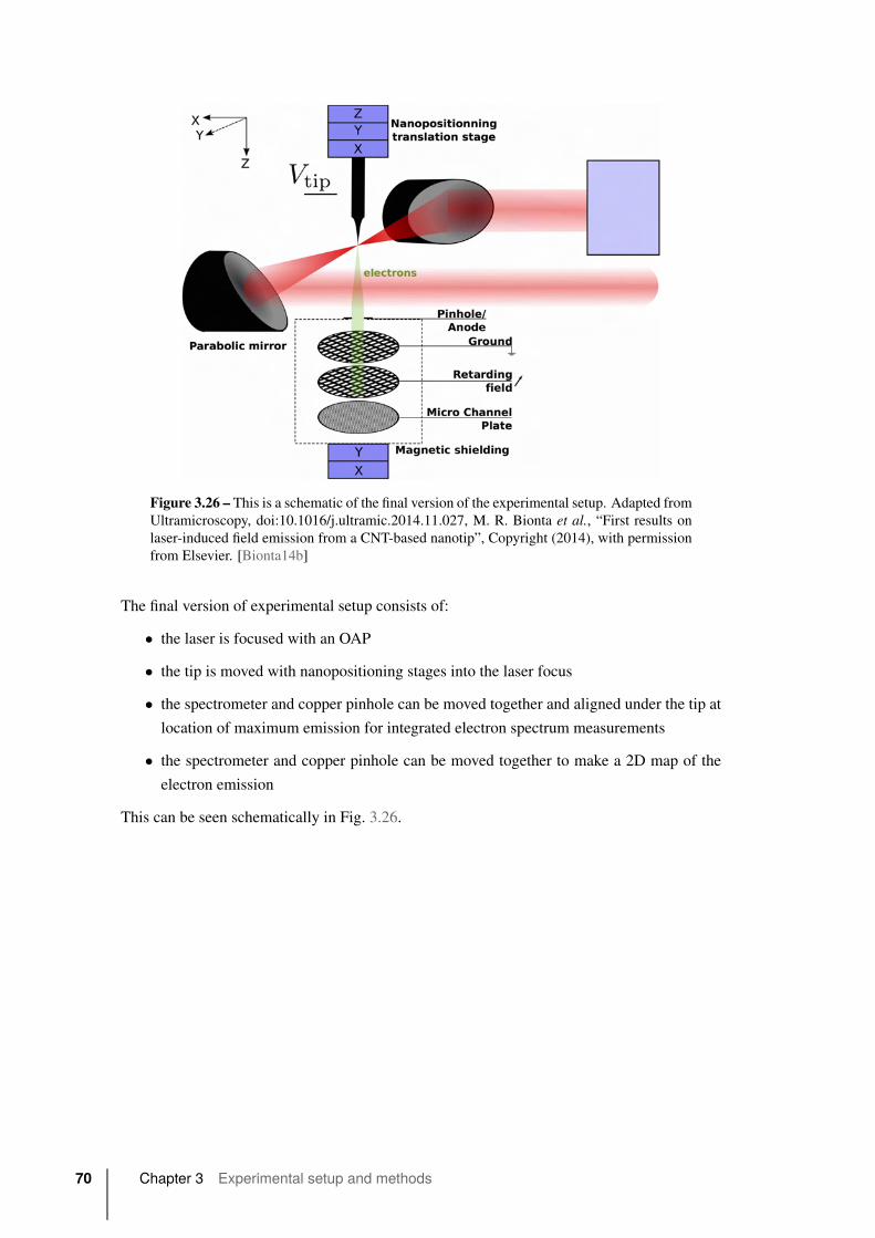
Figure 3.26 – This is a schematic of the final version of the experimental setup. Adapted from
Ultramicroscopy, doi:10.1016/j.ultramic.2014.11.027, M. R. Bionta et al., “First results on
laser-induced field emission from a CNT-based nanotip”, Copyright (2014), with permission
from Elsevier. [Bionta14b]
The final version of experimental setup consists of:
• the laser is focused with an OAP
• the tip is moved with nanopositioning stages into the laser focus
• the spectrometer and copper pinhole can be moved together and aligned under the tip at
location of maximum emission for integrated electron spectrum measurements
• the spectrometer and copper pinhole can be moved together to make a 2D map of the
electron emission
This can be seen schematically in Fig. 3.26.
70 Chapter 3 Experimental setup and methods
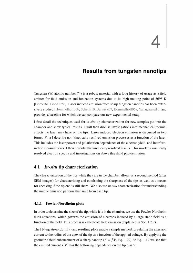
4Results from tungsten nanotips
Tungsten (W, atomic number 74) is a robust material with a long history of usage as a field
emitter for field emission and ionization systems due to its high melting point of 3695 K
[Gomer61, Good Jr56]. Laser induced emission from sharp tungsten nanotips has been exten-
sively studied [Hommelhoff06b, Schenk10, Barwick07, Hommelhoff06a, Yanagisawa10] and
provides a baseline for which we can compare our new experimental setup.
I first detail the techniques used for in-situ tip characterization for new samples put into the
chamber and show typical results. I will then discuss investigations into mechanical thermal
effects the laser may have on the tips. Laser induced electron emission is discussed in two
forms. First I describe non-kinetically resolved emission processes as a function of the laser.
This includes the laser power and polarization dependence of the electron yield, and interfero-
metric measurements. I then describe the kinetically resolved results. This involves kinetically
resolved electron spectra and investigations on above threshold photoemission.
4.1 In-situ tip characterization
The characterization of the tips while they are in the chamber allows us a second method (after
SEM images) for characterizing and confirming the sharpness of the tips as well as a means
for checking if the tip end is still sharp. We also use in-situ characterization for understanding
the unique emission patterns that arise from each tip.
4.1.1 Fowler-Nordheim plots
In order to determine the size of the tip, while it is in the chamber, we use the Fowler-Nordheim
(FN) equations, which governs the emission of electrons induced by a large static field as a
function of the field. This process is called cold field emission (explained in Sec. 1.2.2).
The FN equation (Eq 1.19) and resulting plots enable a simple method for relating the emission
current to the radius of the apex of the tip as a function of the applied voltage. By applying the
geometric field enhancement of a sharp nanotip (F “ βV , Eq. 1.29), to Eq. 1.19 we see that
the emitted current JpV q has the following dependence on the tip bias V :
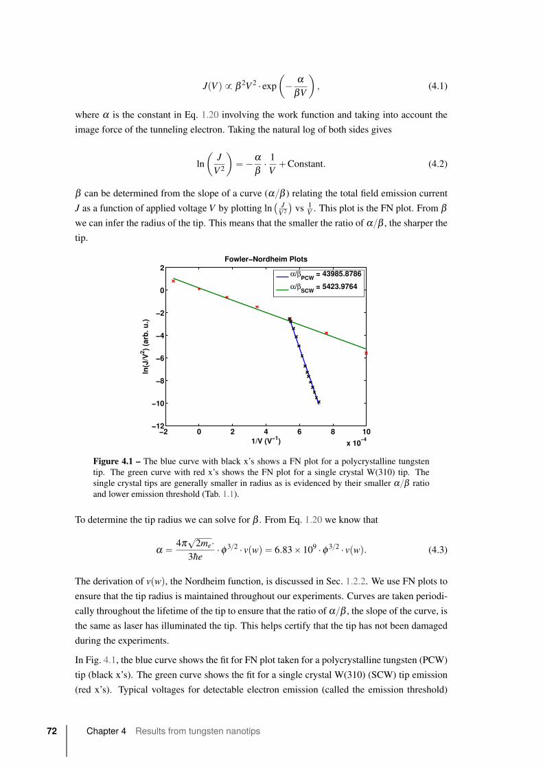
JpV q 9 β 2V 2 ¨ expˆ´ α
βV
˙, (4.1)
where α is the constant in Eq. 1.20 involving the work function and taking into account the
image force of the tunneling electron. Taking the natural log of both sides gives
ln
ˆJ
V 2
˙“´α
β¨ 1V`Constant. (4.2)
β can be determined from the slope of a curve (α{β ) relating the total field emission current
J as a function of applied voltage V by plotting ln` J
V 2
˘vs 1
V . This plot is the FN plot. From βwe can infer the radius of the tip. This means that the smaller the ratio of α{β , the sharper the
tip.
−2 0 2 4 6 8 10
x 10−4
−12
−10
−8
−6
−4
−2
0
2
1/V (V−1)
ln(J
/V2 )
(arb
. u.)
Fowler−Nordheim Plots
α/βPCW
= 43985.8786
α/βSCW
= 5423.9764
Figure 4.1 – The blue curve with black x’s shows a FN plot for a polycrystalline tungsten
tip. The green curve with red x’s shows the FN plot for a single crystal W(310) tip. The
single crystal tips are generally smaller in radius as is evidenced by their smaller α{β ratio
and lower emission threshold (Tab. 1.1).
To determine the tip radius we can solve for β . From Eq. 1.20 we know that
α “ 4π?2me¨
3he¨φ 3{2 ¨ vpwq “ 6.83ˆ109 ¨φ 3{2 ¨ vpwq. (4.3)
The derivation of vpwq, the Nordheim function, is discussed in Sec. 1.2.2. We use FN plots to
ensure that the tip radius is maintained throughout our experiments. Curves are taken periodi-
cally throughout the lifetime of the tip to ensure that the ratio of α{β , the slope of the curve, is
the same as laser has illuminated the tip. This helps certify that the tip has not been damaged
during the experiments.
In Fig. 4.1, the blue curve shows the fit for FN plot taken for a polycrystalline tungsten (PCW)
tip (black x’s). The green curve shows the fit for a single crystal W(310) (SCW) tip emission
(red x’s). Typical voltages for detectable electron emission (called the emission threshold)
72 Chapter 4 Results from tungsten nanotips
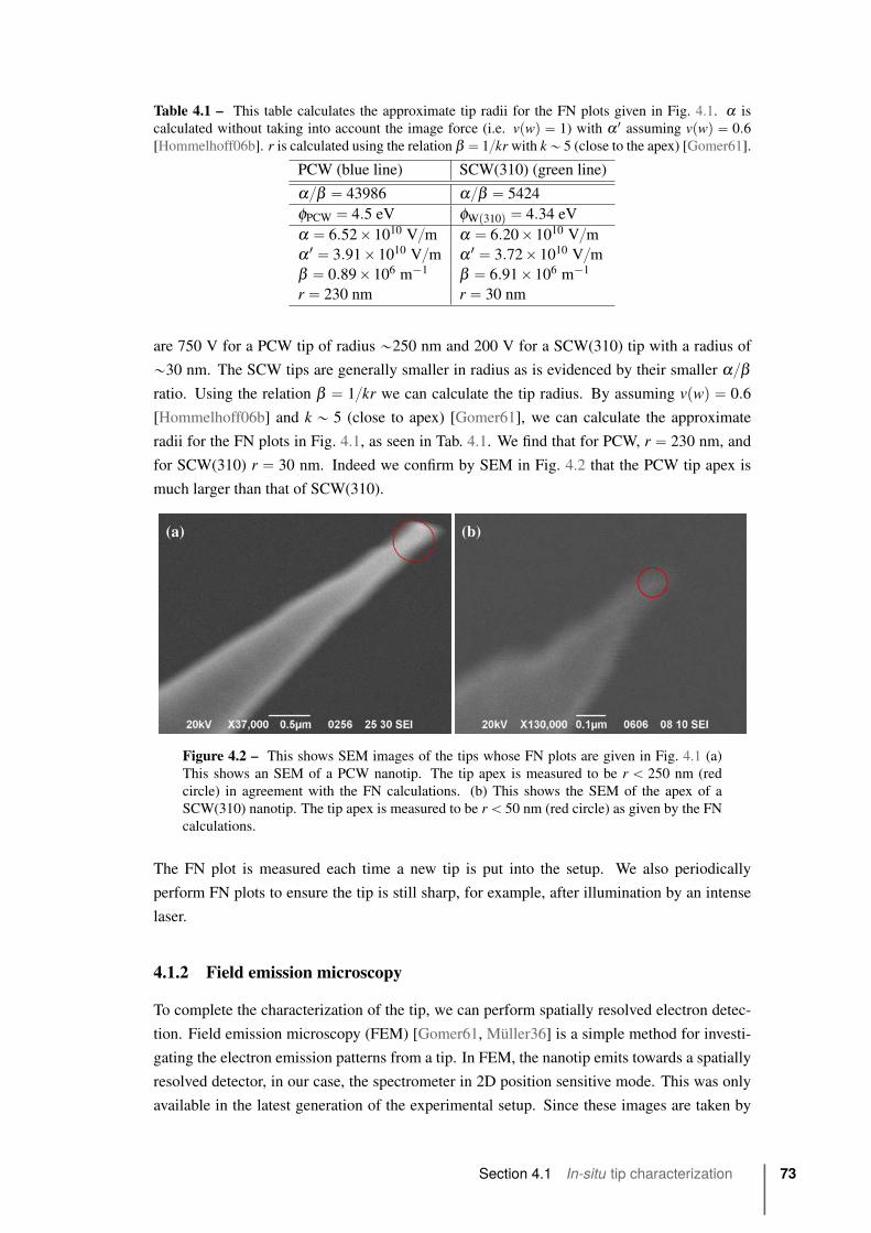
Table 4.1 – This table calculates the approximate tip radii for the FN plots given in Fig. 4.1. α is
calculated without taking into account the image force (i.e. vpwq “ 1) with α 1 assuming vpwq “ 0.6[Hommelhoff06b]. r is calculated using the relation β “ 1{kr with k„ 5 (close to the apex) [Gomer61].
PCW (blue line) SCW(310) (green line)
α{β “ 43986 α{β “ 5424
φPCW “ 4.5 eV φWp310q “ 4.34 eV
α “ 6.52ˆ1010 V{m α “ 6.20ˆ1010 V{mα 1 “ 3.91ˆ1010 V{m α 1 “ 3.72ˆ1010 V{mβ “ 0.89ˆ106 m´1 β “ 6.91ˆ106 m´1
r “ 230 nm r “ 30 nm
are 750 V for a PCW tip of radius „250 nm and 200 V for a SCW(310) tip with a radius of
„30 nm. The SCW tips are generally smaller in radius as is evidenced by their smaller α{βratio. Using the relation β “ 1{kr we can calculate the tip radius. By assuming vpwq “ 0.6
[Hommelhoff06b] and k „ 5 (close to apex) [Gomer61], we can calculate the approximate
radii for the FN plots in Fig. 4.1, as seen in Tab. 4.1. We find that for PCW, r “ 230 nm, and
for SCW(310) r “ 30 nm. Indeed we confirm by SEM in Fig. 4.2 that the PCW tip apex is
much larger than that of SCW(310).
(a) (b)
Figure 4.2 – This shows SEM images of the tips whose FN plots are given in Fig. 4.1 (a)
This shows an SEM of a PCW nanotip. The tip apex is measured to be r ă 250 nm (red
circle) in agreement with the FN calculations. (b) This shows the SEM of the apex of a
SCW(310) nanotip. The tip apex is measured to be r ă 50 nm (red circle) as given by the FN
calculations.
The FN plot is measured each time a new tip is put into the setup. We also periodically
perform FN plots to ensure the tip is still sharp, for example, after illumination by an intense
laser.
4.1.2 Field emission microscopy
To complete the characterization of the tip, we can perform spatially resolved electron detec-
tion. Field emission microscopy (FEM) [Gomer61, Müller36] is a simple method for investi-
gating the electron emission patterns from a tip. In FEM, the nanotip emits towards a spatially
resolved detector, in our case, the spectrometer in 2D position sensitive mode. This was only
available in the latest generation of the experimental setup. Since these images are taken by
Section 4.1 In-situ tip characterization 73

physically moving the spectrometer, they typically take a long time to record, on the order of
1-2 hours per image.
Axis 1 (micron)
Axi
s 2
(mic
ron
)
2D Scan. SCW(310) tip. Vtip = 230 V.
1000 2000 3000 4000 5000 6000 7000 8000−3000
−2000
−1000
0
1000
2000
3000
4000
5000
cou
nts
(lo
gsc
ale)
[ar
b. u
.]
1
3
1E1
3E1
1E2
3E2
1E3
3E3
1
3
1E1
3E1
Figure 4.3 – This shows FEM (spatially resolved emission) for a single crystal tip, with
r “ 50 nm. The W(310) facet has the lowest work function of all so emits at the lowest
threshold and has a higher electron yield than the other facets.
By comparing the FEM images from PCW to SCW we see that the PCW emits from the facets
with the lowest emission thresholds (typically those of W(310)). We can see that by choosing
W(310) allows the maximum number of electrons to be emitted and collected. Fig. 4.3 shows
a FEM image for a (310) oriented tungsten tip. We can then position the spectrometer such
that the highest brightness emission facet is oriented towards the entrance slit. We also can
periodically take scans to confirm that the tip has not broken after strong laser illumination,
forming new sharp edges where emission might occur.
4.2 Thermal damage studies
For high repetition rate, high mean power lasers, thermal effects are generally non-negligible
which can lead to tip destruction. Evidence of damage to tips was sometimes observed after
laser irradiation; however, it was unclear if this damage was thermal damage, or mechanical
damage possibly from tip transportation. Because of this, we investigated the thermal effects
of the oscillator laser on tungsten tips.
A tungsten “comb” was fabricated such that we could systematically look at the thermal effects
in tungsten. The comb consisted of a silicon substrate onto which many tungsten tips were
pasted. Each tip was then systematically irradiated in turn at a specific laser power and for a
specific amount of time. We empirically looked for laser damage by comparing SEM images
from before and after laser irradiation. The laser was focused with an on-axis spherical mirror
with a focal length of either 7 mm or 50 mm to greatly vary the intensity. Due to the use of
adhesive to attach the tips to the substrate, the application of a bias voltage was not possible.
This means there was no way of extracting the emitted electrons from the irradiated tips. The
74 Chapter 4 Results from tungsten nanotips

alignment of the tips was done at low laser intensity using the diffraction scattering seen by
the CCD camera. For example, tip A4 was aligned with 250 μW of average power (4.11ˆ107 W cm´2 peak intensity), a procedure which took „10 minutes before being illuminated
with 10 mW (1.64ˆ 109 W cm´2). The intensity of the illumination power is an order
of magnitude less than the minimum laser intensity with which we tested. The long focal
length also means that there was a long Rayleigh ranges and thus the tip was more likely in
the focus of the laser. Two tips were not intentionally illuminated with the laser for control
purposes.
Comparisons of SEM images before and after laser irradiation showed no significant modifica-
tion in the nanotip structures. None of the tips illuminated with the longer focal length showed
any signs of damage. Fig. 4.4 shows before and after SEM images of tip B1 after illumination
with 200 mW of average power for 24 hours with a focal spot size of „25 μm, corresponding
to a peak intensity of 3.29ˆ109 W cm´2. No visible damage is seen.
(a) (b)
Figure 4.4 – (a) A SEM of tip B1 before laser irradiation. (b) SEM of the same tip after
irradiation with 200 mW of average power for 24 hours with a focal spot size of „25 μm,
corresponding to a peak intensity of 3.29ˆ109 W cm´2. No visible damage is seen.
C2 was illuminated with the highest laser intensity for the longest time, 8.38ˆ1011 W cm´2 for
24 hours. This corresponds to 100 mW average power with a spot size of 3 μm due to the
shorter focal length. A small drop appears on the side of the tip in after illumination with the
laser. This could potentially be due to melting of the tungsten. The apex of the tip is also
slightly bent, probably due to the laser irradiation.
Scans from a residual gas analyzer (RGA) were taken during each of the tests, however, no
particular species were detected. As we could not detect emitted electrons by the tips due
to the construction of the comb, we were not sure of the exact alignment of the tips into the
focus. Apart form this, and even though the before and after SEM images were taking by two
different people and thus the resolutions and areas investigated were not the same, we saw no
evidence of laser induced thermal damage due to our tests. A complete data set of before and
after SEM photos can be seen in App. B.
Section 4.2 Thermal damage studies 75

(a) (b)
Figure 4.5 – (a) A SEM of tip C2 before laser irradiation. (b) SEM of after irradiation with
100 mW of average power for 24 hours with a focal spot size of „3 μm, corresponding to a
peak intensity of 8.38ˆ1011 W cm´2. A small droplet is seen on the side of the tip and the
apex is slightly bent after irradiation.
4.3 Laser induced emission
In order to test the validity of our setup, we investigate laser induced emission phenomenon in
the Keldysh regime from the electron emission from the tip. Much of this discussion comes
from and is augmented upon [Bionta14a].
To extract the electrons emitted from the tip, a small DC field, Vtip, typically between 20–50 V,
is applied to the tip. After the laser is prealigned (Sec. 3.6.1) on the tip, it is carefully moved
around in the focus to look for electron emission.
4.3.1 Laser polarization dependence
The electron emission induced by the laser is highly polarization dependent. This is because
the photofield emission depends only on the component of the laser electric field which is nor-
mal to the surface [Venus83], which at the tip apex, is the component parallel to the tip axis.
The optical field enhancement, due to the sub-wavelength size of the nanotip, is larger for po-
larizations parallel to the tip axis. By contrast, laser induced thermally enhanced field emission
is most efficient at polarizations perpendicular to the tip axis [Barwick07, Hadley85].
When the tip is misaligned in the laser focus, the focus illuminates the shank of the tip. This
strongly influences the heating of the tip, emphasizing thermally enhanced field emission.
This provides a simple means of checking the alignment of the tip in the laser focus. If the
tip is properly aligned, the focus will not heat the tip and there will not be any emission for
polarizations perpendicular to the tip axis. By measuring the electron yield as a function of
laser polarization, we can easily see if the tip is well aligned or not.
The polarization dependence of a well aligned tip is seen in Fig. 4.6 [Bionta14a]. The tip is
illuminated with 150 mW (2.4 nJ/pulse, 8ˆ 1011 W cm´2) from the output of the oscillator
with Vtip= 50 V. The blue x’s show the electron yield as a function of the laser polarization
(θ ) with respect to the tip axis. A polarization of 0˝ indicates that the laser field is parallel
to the tip axis; likewise, a polarization of 90˝ means that the field is orthogonal to the tip
76 Chapter 4 Results from tungsten nanotips

Figure 4.6 – Electron yield as a function of laser polarization (θ ) with respect to the tip axis.
Polarizations parallel to the tip axis (polarization angles of 0 and 90) have the highest electron
emission, by contrast, perpendicular polarizations (angles of 180 and 270) have negligible
emission. The experimental data (blue x’s) are fit with the form cos2npθq (green line), where
n is the number of photon absorbed by the system before emission. Figure adapted from
[Bionta14a].
0 45 90 135 1800
2
4
6
8
10
12
14
16x 10
4 Misaligned tip polarization dependence
polarization angle
co
un
ts (
arb
.u.)
Figure 4.7 – This shows the electron yields as a function of polarization angle for a mis-
aligned tip. As in Fig. 4.6, an angle of 0 corresponds to a polarization parallel to the tip axis,
and an angle of 90 is perpendicular to the axis.
axis. As expected, maximum electron yield is found at polarization angles of 0 and 180,
with a minimum at 90 and 270 and a contrast of „3500:1. Fig. 4.7 shows the polarization
dependence for a misaligned tip. Notice the counts that appear for orthogonal polarization.
Maximizing the contrast demonstrates proper alignment. The polarization dependence is also
very useful to check that the tip is still fully intact and not damaged.
Section 4.3 Laser induced emission 77
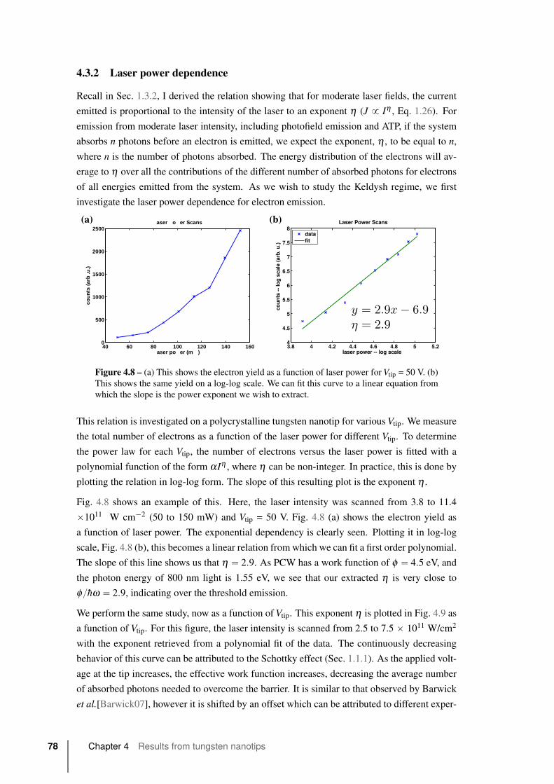
4.3.2 Laser power dependence
Recall in Sec. 1.3.2, I derived the relation showing that for moderate laser fields, the current
emitted is proportional to the intensity of the laser to an exponent η (J 9 Iη , Eq. 1.26). For
emission from moderate laser intensity, including photofield emission and ATP, if the system
absorbs n photons before an electron is emitted, we expect the exponent, η , to be equal to n,where n is the number of photons absorbed. The energy distribution of the electrons will av-
erage to η over all the contributions of the different number of absorbed photons for electrons
of all energies emitted from the system. As we wish to study the Keldysh regime, we first
investigate the laser power dependence for electron emission.
40 60 80 100 120 140 1600
500
1000
1500
2000
2500
aser po er (m )
coun
ts (a
rb .u
.)
aser o er Scans(a)
3.8 4 4.2 4.4 4.6 4.8 5 5.24
4.5
5
5.5
6
6.5
7
7.5
8
laser power -- log scale
co
un
ts -
- lo
g s
ca
le (
arb
. u
.)
Laser Power Scans
data
fit
(b)
Figure 4.8 – (a) This shows the electron yield as a function of laser power for Vtip = 50 V. (b)
This shows the same yield on a log-log scale. We can fit this curve to a linear equation from
which the slope is the power exponent we wish to extract.
This relation is investigated on a polycrystalline tungsten nanotip for various Vtip. We measure
the total number of electrons as a function of the laser power for different Vtip. To determine
the power law for each Vtip, the number of electrons versus the laser power is fitted with a
polynomial function of the form αIη , where η can be non-integer. In practice, this is done by
plotting the relation in log-log form. The slope of this resulting plot is the exponent η .
Fig. 4.8 shows an example of this. Here, the laser intensity was scanned from 3.8 to 11.4
ˆ1011 W cm´2 (50 to 150 mW) and Vtip = 50 V. Fig. 4.8 (a) shows the electron yield as
a function of laser power. The exponential dependency is clearly seen. Plotting it in log-log
scale, Fig. 4.8 (b), this becomes a linear relation from which we can fit a first order polynomial.
The slope of this line shows us that η “ 2.9. As PCW has a work function of φ “ 4.5 eV, and
the photon energy of 800 nm light is 1.55 eV, we see that our extracted η is very close to
φ{hω “ 2.9, indicating over the threshold emission.
We perform the same study, now as a function of Vtip. This exponent η is plotted in Fig. 4.9 as
a function of Vtip. For this figure, the laser intensity is scanned from 2.5 to 7.5 ˆ 1011 W/cm2
with the exponent retrieved from a polynomial fit of the data. The continuously decreasing
behavior of this curve can be attributed to the Schottky effect (Sec. 1.1.1). As the applied volt-
age at the tip increases, the effective work function increases, decreasing the average number
of absorbed photons needed to overcome the barrier. It is similar to that observed by Barwick
et al.[Barwick07], however it is shifted by an offset which can be attributed to different exper-
78 Chapter 4 Results from tungsten nanotips
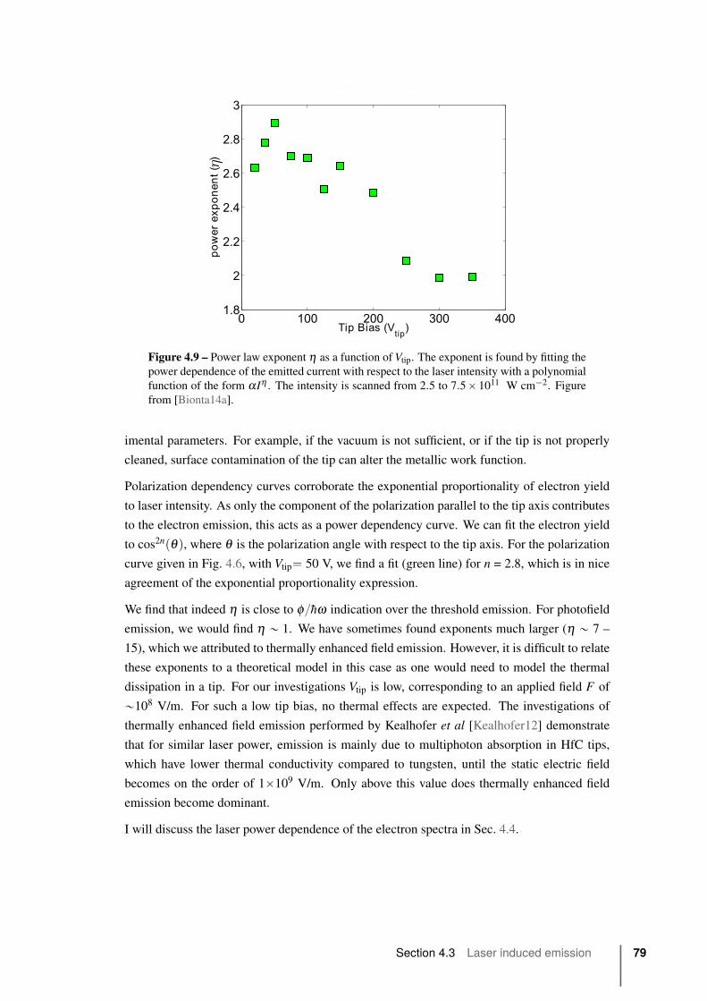
Figure 4.9 – Power law exponent η as a function of Vtip. The exponent is found by fitting the
power dependence of the emitted current with respect to the laser intensity with a polynomial
function of the form αIη . The intensity is scanned from 2.5 to 7.5ˆ1011 W cm´2. Figure
from [Bionta14a].
imental parameters. For example, if the vacuum is not sufficient, or if the tip is not properly
cleaned, surface contamination of the tip can alter the metallic work function.
Polarization dependency curves corroborate the exponential proportionality of electron yield
to laser intensity. As only the component of the polarization parallel to the tip axis contributes
to the electron emission, this acts as a power dependency curve. We can fit the electron yield
to cos2npθq, where θ is the polarization angle with respect to the tip axis. For the polarization
curve given in Fig. 4.6, with Vtip“ 50 V, we find a fit (green line) for n = 2.8, which is in nice
agreement of the exponential proportionality expression.
We find that indeed η is close to φ{hω indication over the threshold emission. For photofield
emission, we would find η „ 1. We have sometimes found exponents much larger (η „ 7 –
15), which we attributed to thermally enhanced field emission. However, it is difficult to relate
these exponents to a theoretical model in this case as one would need to model the thermal
dissipation in a tip. For our investigations Vtip is low, corresponding to an applied field F of
„108 V/m. For such a low tip bias, no thermal effects are expected. The investigations of
thermally enhanced field emission performed by Kealhofer et al [Kealhofer12] demonstrate
that for similar laser power, emission is mainly due to multiphoton absorption in HfC tips,
which have lower thermal conductivity compared to tungsten, until the static electric field
becomes on the order of 1ˆ109 V/m. Only above this value does thermally enhanced field
emission become dominant.
I will discuss the laser power dependence of the electron spectra in Sec. 4.4.
Section 4.3 Laser induced emission 79

4.3.3 Two pulse interferometry
By adding a beam splitter and delay line to the beamline allows us to build a Michelson in-
terferometer (Fig. 4.10), to send two pulses onto the tip separated by a time delay of τ . We
investigate interferometric autocorrelations of the laser pulse using the non-linear response of
the tip. This refers to an optical interferometer. The pulses interfere before interacting with the
nanotip. The emitted electrons are then a function of the interference of the two laser pulses
(i.e. delay between the two pulses). This type of autocorrelation trace can be used to verify
the pulse duration at the interaction region of the experiment.
��
Figure 4.10 – This shows the schematic layout of a Michelson interferometer with a delay of
τ between pulses.
−100 −50 0 50 1000
500
1000
1500
2000
2500
3000
3500
Delay between pulses, τ, (fs)
Co
un
ts (
arb
. u.)
Figure 4.11 – Number of electrons as a function of delay between optical pulses, τ .
Fig. 4.11 shows the number of electrons as a function of the delay between the two laser
pulses. The peak to base ratio is approximately equal to 17. This can be used to confirm
the non linearity of the emission, and gives a power exponent η « 2.6. The width of the
autocorrelation trace could be used to retrieve the optical pulse duration, knowing the power
80 Chapter 4 Results from tungsten nanotips

exponent. While the trace confirms that the pulse is short, we preferred to use the complete
pulse measurement provided by the LX Spider to characterize our laser pulses.
We can investigate that the electron emission is due to the electric field of the laser As thermally
enhanced emission is long lasting (on the order of 100s of fs [Kealhofer13]), we would see
emission from the tip long after the application of the first pulse onto the tip. The second pulse
would simply enhance the emission from the first pulse. In our autocorrelation traces we see a
flat baseline for delays greater than the pulse duration, thus indicating that there are no thermal
effects in this case.
4.3.4 Photoelectron spectra
� � �� �����
���
���
���
���
���
�� ������
���
�������� ����������������
�� �����������������
��� ���� ��!�����"!#������������!�����"
� � �� ���
�
�
�
�
�
�$����
�� ������
%��������������
�� �����������������
��� ���� ��!�����"!#������������!�����"
Figure 4.12 – This shows photoelectron spectra from a W(310) nanotip. For this spectrum
an extraction voltage of Vtip = 20 V, and a laser power of 50 mW (0.8 nJ/pulse, 1.52ˆ 1012
W cm´2 peak intensity) was used. The direct spectrometer output, an integrated spectrum, is
shown by blue dots. The kinetically resolved photoelectron spectrum is shown by the green
line. Note ATP peaks up to order n “ 9 are easily observable in the spectrum. The inset
shows the spectra in linear scale. Only the first four ATP peaks are easily resolvable in this
scale, thus it is beneficial to plot the spectra in log scale.
Fig. 4.12 shows a photoelectron spectrum from aW(310) nanotip. For this spectrum, an extrac-
tion voltage ofVtip = 20 V, and a laser power of 50 mW (0.8 nJ/pulse, 1.52ˆ1012 W cm´2 peak
intensity) was used. The kinetic energy acquired from the appliedVtip has been subtracted. The
conditions are such that there is less than one electron emitted per laser pulse to avoid Coulomb
space charge effects. The spectrometer records the number of electrons with a higher energy
than the retarding field with a scan resolution of 0.05 V over 500 ms, thus makes an integrated
Section 4.3 Laser induced emission 81
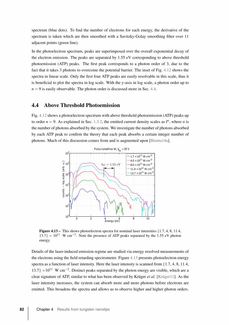
spectrum (blue dots). To find the number of electrons for each energy, the derivative of the
spectrum is taken which are then smoothed with a Savitzky-Golay smoothing filter over 11
adjacent points (green line).
In the photoelectron spectrum, peaks are superimposed over the overall exponential decay of
the electron emission. The peaks are separated by 1.55 eV corresponding to above threshold
photoemission (ATP) peaks. The first peak corresponds to a photon order of 3, due to the
fact that it takes 3 photons to overcome the potential barrier. The inset of Fig. 4.12 shows the
spectra in linear scale. Only the first four ATP peaks are easily resolvable in this scale, thus it
is beneficial to plot the spectra in log scale. With the y-axis in log scale, a photon order up to
n“ 9 is easily observable. The photon order is discussed more in Sec. 4.4.
4.4 Above Threshold Photoemission
Fig. 4.12 shows a photoelectron spectrum with above threshold photoemission (ATP) peaks up
to order n“ 9. As explained in Sec. 1.3.2, the emitted current density scales as In, where n is
the number of photons absorbed by the system. We investigate the number of photons absorbed
by each ATP peak to confirm the theory that each peak absorbs a certain integer number of
photons. Much of this discussion comes from and is augmented upon [Bionta14a].
� � � � � �����
���
���
���
���
��
���
�� �������
���������������������� ������
����� ���������� !����" #����
��$�%���� ��&��
����������&��
����������&��
�����������&��
��� �������&��
Figure 4.13 – This shows photoelectron spectra for nominal laser intensities {1.7, 4, 8, 11.4,
13.7} ˆ 1011 W cm´2. Note the presence of ATP peaks separated by the 1.55 eV photon
energy.
Details of the laser-induced emission regime are studied via energy resolved measurements of
the electrons using the field retarding spectrometer. Figure 4.13 presents photoelectron energy
spectra as a function of laser intensity. Here the laser intensity is scanned from {1.7, 4, 8, 11.4,
13.7} ˆ1011 W cm´2. Distinct peaks separated by the photon energy are visible, which are a
clear signature of ATP, similar to what has been observed by Krüger et al. [Krüger11]. As the
laser intensity increases, the system can absorb more and more photons before electrons are
emitted. This broadens the spectra and allows us to observe higher and higher photon orders.
82 Chapter 4 Results from tungsten nanotips
At low laser intensity (blue curve, Fig. 4.13), we can only see the distinguish the first two ATP
peaks (up to n “ 4); however, at high laser intensity (purple curve) we can easily see photon
orders up to n“ 9.
We confirm these emission mechanisms, and photon order, with an energy-selective, laser-
power dependence measurement of these ATP peaks. Results are shown in Fig. 4.14 for an
experiment with Vtip “ 30 V and laser peak intensities from 1 to 3.6ˆ 1011 W/cm2. Individual
peaks are indicated by the same color throughout the figure. Fig. 4.14 (a) shows the energy
spectrum recorded at 3.6 ˆ 1011 W/cm2, where different ATP peaks are identified with differ-
ent colors. Fig. 4.14 (b) shows the electron count rate versus laser intensity plotted in log scale.
Each line corresponds to one peak of the photoelectron spectra as defined in Fig. 4.14 (a). The
electron yield is obtained by integrating over all of the energy window corresponding to each
peak. We retrieve the exponent of each energy peak by extracting the slope of each fitted line.
Fig. 4.14 (c) shows the retrieved power exponents of the four peaks from about 3 to 6, with
corresponding error bars relative to the fit.
0 5 10
102
103
104
105
Electron energy − tip bias (eV)
Ele
ctro
n co
unt r
ate
(a. u
.)
(a) 1 1.3 1.6 2.0 2.5 3.21
10
100
1000
10000
100000
1000000
Laser Intensity (× 1011 W/cm²) − log scale
Ele
ctro
ns r
ate
(a.u
.)
(b) 1 2 3 40
1
2
3
4
5
6
7
Peak number
Pow
er
exponent
(c)
Figure 4.14 – (a) Electron energy spectrum obtained for a Vtip “ 30 V and laser intensity
of 3.6ˆ 1011 W cm´2. The different ATP peaks are identified by the different colors. (b)
Electron yield versus laser intensity plotted for each ATP peak. The dots are the experimental
values, and the lines are the fit from which we retrieve the exponent. (c) Power exponents for
each peak. As expected for ATP, we obtain exponents from 3 to 6. Reprinted with permission
from [Bionta14a].
As expected for ATP, each peak corresponds to a different number of absorbed photons, there-
fore corresponding to a different exponent. The first peak is close to 3 (3.4 ˘ 0.1), since the
work function of polycrystalline tungsten (φ “ 4.5 eV) is roughly equal to 3 times the pho-
ton energy (3 ˆ 1.55 eV “ 4.65 eV). The second, third and fourth peaks have respective
exponents of 4.0 ˘ 0.1, 5.0 ˘ 0.1, and 6.5 ˘ 0.3, showing that in this part of the spectrum
the system absorbs 4, 5 and 6 photons before electrons leave the laser focus. This confirms
that in our case, the photoelectron emission is mainly due to multiphoton absorption, with-
out any contribution of photofield emission. These experiments were reproduced for the two
first peaks with various experimental conditions (different tips, different focusing), and with
different energy selections–choosing electrons from within the entire peak, or just at the max-
imum of the peak. The values of the exponents are reproducible to within 10 % for several
tips.
The Keldysh parameter can be calculated from Eq. 1.22. For PCW φ “ 4.5 eV and a laser
wavelength of 800 nm of intensity 3.6 ˆ 1011 W/cm2, we find the Keldysh parameter to be
γ “ 10, before any enhancement from the tip. γ ą 1 means that we should not be in the
Section 4.4 Above Threshold Photoemission 83

optical tunneling regime, and indeed we do not see the spectral plateau signature of rescat-
tering. However, for similar laser intensities (meaning a similar Keldysh parameter), Krüger
et al. (group of P. Hommelhoff) observed spectral plateaus indicating optical tunneling and
rescattering [Krüger12b]. The group reported a tip radius a factor of two smaller than ours,
indicating there is more geometric field enhancement near the apex. They also have a pulse
duration of their laser of only 6 fs. Our longer, 20 fs pulses may be suppressing the rescatter-
ing effect as the energy is spread out over a longer period of time. This may cause short-term
thermal effects which overtake the emission mechanism for high energies.
4.5 Summary
We investigate electron emission from a tungsten nanotip in order to form a baseline to com-
pare our new experimental setup to already existing experiments.
We have a variety of methods for in-situ characterization of the tip. Using FN plots we can
calculate the tip radius. We use the slope of these plots to check that the tip radius stays the
same throughout our investigations. Typical tip radii are on the order of 250 nm for PCW tips
and 30 nm for SCW(310) tips. We also use FEM-like plots to investigate spatially resolved
emission patterns from the tip. From these we see that there is indeed only one emission site
from SCW(310) tips and that it is facing the detector.
The damage threshold due to laser irradiation was systematically and empirically studied.
These test proved to be inconclusive, due to uncertainties in the laser alignment on the tips and
the lack of visible damage to the tips.
Polarization dependence curves were used to check the alignment of the tip in the laser focus.
A good contrast of „3500:1 was found for a well aligned tip. The laser power dependence
gives us the average number of photons absorbed by the system before an electron was emitted.
We find a decrease in this number as the applied voltage increases, due to the Schottky effect.
Kinetically resolved power dependencies were also measured and for each individual ATP
peak up to a photon order of n “ 6. We confirmed that each peak corresponds to a different
number of absorbed photons.
The experiments on tungsten allow us to validate our experimental setup in comparison to al-
ready established results. We were also able to familiarize ourselves with the new experimental
setup as well as techniques for working with nanostructures. With a correct understanding of
our results and experimental setup, we can turn to other samples for investigation.
84 Chapter 4 Results from tungsten nanotips
5Carbon Cone nanoTips (CCnT)
The investigation of electron emission from novel tip materials such as carbon nanotubes has
yielded interesting properties for cold field emission. These new samples have a very dif-
ferent structure and electronic properties than conventional metallic nanotips. We believe
that the mechanical and electrical properties the carbon tips present for cold field emission
are a promising start towards the observation of strong field phenomenon resulting from the
laser-tip interaction. Our collaboration with CEMES allows us access to a novel new nano-
tip type based on a central carbon nanotube, surrounded by concentric graphene sheets to
form a conical shape. Extensive studies on cold field emission from these tips can be found
in [deKnoop14, Houdellier12, Houdellier15] and show promising results. The mechanisms
behind electron emission from these tips is unknown and we investigate the properties from
laser-induced emission from these carbon based nanotips.
I first give a detailed description of the material and structural properties of the carbon nano-
tips. I then discuss the characterization of our tips using SEM, FN and FEM techniques.
Laser induced electron emission is presented for polarization dependency curves as well as
kinetically resolved photoelectron spectra. Damage to the samples was observed after laser
irradiation, so systematic studies on the damage limits of the carbon tips are detailed. Some of
the results presented in this chapter are published in [Bionta14b].
5.1 Description of a Carbon Cone nanoTip (CCnT)
We use Carbon Cone nanoTips (CCnT) in collaboration with CEMES. At CEMES, they focus
on the synthesis of the tips as well as cold field emission properties for use as a field emitter
for electron microscopy. My group aims to investigate the interaction of such a tip with an
optical field to study the laser-induced emission properties from a CCnT.
The CCnT is a tip based on a conical form of carbon. These tips have a work function of
φ “ 5 eV [Houdellier12], and an apex diameter of a few nm. The center of the cone is a
single, multi-wall carbon nanotube (CNT) surrounded by concentric graphene sheets to form
a conical shape. The interior structure of the sheets can be seen via transmission electron
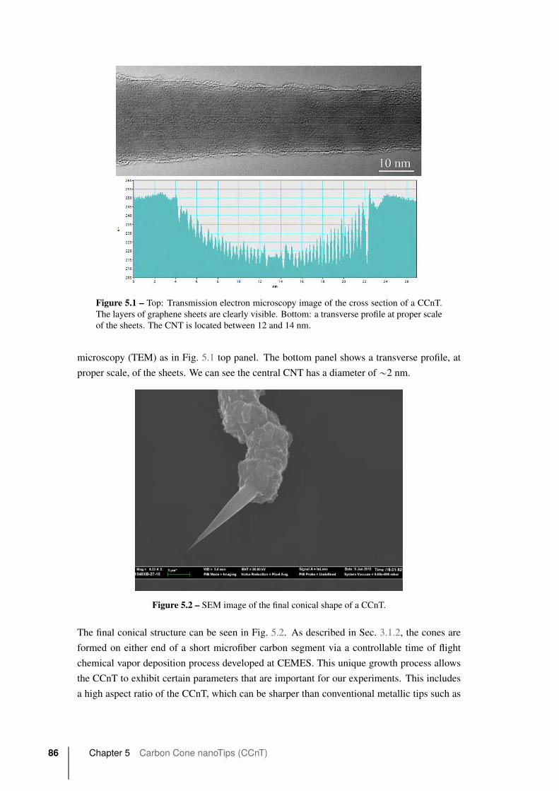
Figure 5.1 – Top: Transmission electron microscopy image of the cross section of a CCnT.
The layers of graphene sheets are clearly visible. Bottom: a transverse profile at proper scale
of the sheets. The CNT is located between 12 and 14 nm.
microscopy (TEM) as in Fig. 5.1 top panel. The bottom panel shows a transverse profile, at
proper scale, of the sheets. We can see the central CNT has a diameter of „2 nm.
Figure 5.2 – SEM image of the final conical shape of a CCnT.
The final conical structure can be seen in Fig. 5.2. As described in Sec. 3.1.2, the cones are
formed on either end of a short microfiber carbon segment via a controllable time of flight
chemical vapor deposition process developed at CEMES. This unique growth process allows
the CCnT to exhibit certain parameters that are important for our experiments. This includes
a high aspect ratio of the CCnT, which can be sharper than conventional metallic tips such as
86 Chapter 5 Carbon Cone nanoTips (CCnT)

tungsten or gold, and has a smaller apex size leading to higher geometric field enhancement in
the vicinity of the tip.
The static field emission properties of this tip have been extensively studied [Houdellier12,
deKnoop14, Houdellier15]. Characterization of the cold field emission has shown high bright-
ness and coherency in the emitted electrons, on the order of 3 times brighter than a standard
tungsten emitter [Houdellier12]. The tip has demonstrated robustness in lifetime in current
field emission gun installations [Houdellier12, Houdellier15].
Investigations into ways to grow CCnTs with doped CNTs is currently underway in collabo-
ration with CEMES and the University of Zaragoza. There is theoretical evidence of changes
in the emission properties of CNTs due to doping. These include a decreased work function
promoting enhanced field emission [Qiao07, Ghosh10]. By tailoring the growth process of the
CCnTs we hope to promote certain emission properties we wish to exhibit, such as enhanced
directionality of electron emission.
5.2 CCnT characterization
5.2.1 Scanning electron microscopy
As the CCnTs are mounted onto tungsten tips in a FIB environment (Sec. 3.1.2), the tips are
characterized as they are made. Fig. 5.3 shows the SEM of a finish mounted tip on a tungsten
tip.
Figure 5.3 – This shows the SEM of a CCnT after it has been mounted onto a tungsten tip.
As the CCnTs are randomly formed and dispersed over the substrate, choosing a perfectly
straight cone is not always evident. Fig. 5.3 shows an example of a CCnT with an highly
angled cone with respect to the carbon fiber and tungsten tip. The placement of the fiber on
the tungsten base also shows some of the irregularities that occur from tip to tip due to the
in-house fabrication methods.
Section 5.2 CCnT characterization 87
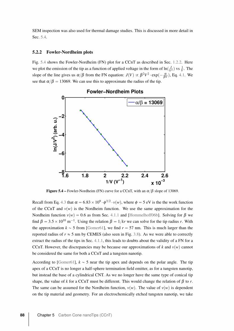
SEM inspection was also used for thermal damage studies. This is discussed in more detail in
Sec. 5.4.
5.2.2 Fowler-Nordheim plots
Fig. 5.4 shows the Fowler-Nordheim (FN) plot for a CCnT as described in Sec. 1.2.2. Here
we plot the emission of the tip as a function of applied voltage in the form of lnp JV 2 q vs 1
V . The
slope of the line gives us α{β from the FN equation: JpV q 9 β 2V 2 ¨ expp´ αβV q, Eq. 4.1. We
see that α{β “ 13069. We can use this to approximate the radius of the tip.
1.6 1.8 2 2.2 2.4 2.6x 10
−3
−8
−6
−4
−2
0
1/V (V−1)
ln(J
/V2 )
(arb
. u.)
Fowler−Nordheim Plots
α/β = 13069
Figure 5.4 – Fowler-Nordheim (FN) curve for a CCnT, with an α{β slope of 13069.
Recall from Eq. 4.3 that α “ 6.83ˆ109 ¨φ 3{2 ¨ vpwq, where φ “ 5 eV is the the work function
of the CCnT and vpwq is the Nordheim function. We use the same approximation for the
Nordheim function vpwq “ 0.6 as from Sec. 4.1.1 and [Hommelhoff06b]. Solving for β we
find β “ 3.5ˆ1010 m´1. Using the relation β “ 1{kr we can solve for the tip radius r. With
the approximation k „ 5 from [Gomer61], we find r “ 57 nm. This is much larger than the
reported radius of r « 5 nm by CEMES (also seen in Fig. 3.8). As we were able to correctly
extract the radius of the tips in Sec. 4.1.1, this leads to doubts about the validity of a FN for a
CCnT. However, the discrepancies may be because our approximations of k and vpwq cannotbe considered the same for both a CCnT and a tungsten nanotip.
According to [Gomer61], k „ 5 near the tip apex and depends on the polar angle. The tip
apex of a CCnT is no longer a half-sphere termination field emitter, as for a tungsten nanotip,
but instead the base of a cylindrical CNT. As we no longer have the same type of conical tip
shape, the value of k for a CCnT must be different. This would change the relation of β to r.The same can be assumed for the Nordheim function, vpwq. The value of vpwq is dependent
on the tip material and geometry. For an electrochemically etched tungsten nanotip, we take
88 Chapter 5 Carbon Cone nanoTips (CCnT)
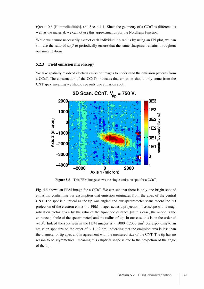
vpwq “ 0.6 [Hommelhoff06b], and Sec. 4.1.1. Since the geometry of a CCnT is different, as
well as the material, we cannot use this approximation for the Nordheim function.
While we cannot necessarily extract each individual tip radius by using an FN plot, we can
still use the ratio of α{β to periodically ensure that the same sharpness remains throughout
our investigations.
5.2.3 Field emission microscopy
We take spatially resolved electron emission images to understand the emission patterns from
a CCnT. The construction of the CCnTs indicates that emission should only come from the
CNT apex, meaning we should see only one emission spot.
Axis 1 (micron)
Axi
s 2
(mic
ron
)
2D Scan. CCnT. Vtip
= 750 V.
−2000 0 2000−4000
−3000
−2000
−1000
0
1000
2000
cou
nts
(lo
g s
cale
) [a
rb. u
.]
1
3
1E1
3E1
1E2
3E2
1E3
3E3
Figure 5.5 – This FEM image shows the single emission spot for a CCnT.
Fig. 5.5 shows an FEM image for a CCnT. We can see that there is only one bright spot of
emission, confirming our assumption that emission originates from the apex of the central
CNT. The spot is elliptical as the tip was angled and our spectrometer scans record the 2D
projection of the electron emission. FEM images act as a projection microscope with a mag-
nification factor given by the ratio of the tip-anode distance (in this case, the anode is the
entrance pinhole of the spectrometer) and the radius of tip. In our case this is on the order of
„106. Indeed the spot seen in the FEM images is „ 1000ˆ 2000 μm2 corresponding to an
emission spot size on the order of „ 1ˆ 2 nm, indicating that the emission area is less than
the diameter of tip apex and in agreement with the measured size of the CNT. The tip has no
reason to be asymmetrical, meaning this elliptical shape is due to the projection of the angle
of the tip.
Section 5.2 CCnT characterization 89
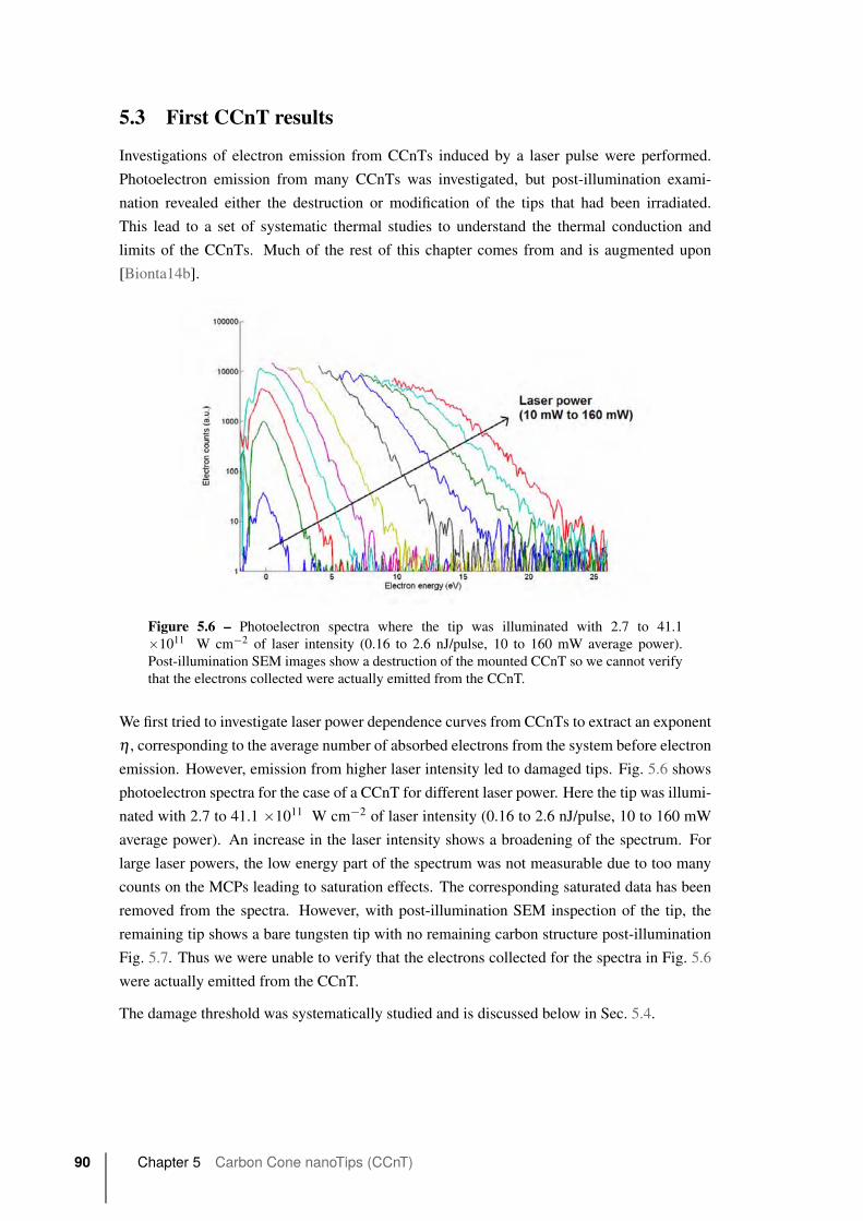
5.3 First CCnT results
Investigations of electron emission from CCnTs induced by a laser pulse were performed.
Photoelectron emission from many CCnTs was investigated, but post-illumination exami-
nation revealed either the destruction or modification of the tips that had been irradiated.
This lead to a set of systematic thermal studies to understand the thermal conduction and
limits of the CCnTs. Much of the rest of this chapter comes from and is augmented upon
[Bionta14b].
Figure 5.6 – Photoelectron spectra where the tip was illuminated with 2.7 to 41.1
ˆ1011 W cm´2 of laser intensity (0.16 to 2.6 nJ/pulse, 10 to 160 mW average power).
Post-illumination SEM images show a destruction of the mounted CCnT so we cannot verify
that the electrons collected were actually emitted from the CCnT.
We first tried to investigate laser power dependence curves from CCnTs to extract an exponent
η , corresponding to the average number of absorbed electrons from the system before electron
emission. However, emission from higher laser intensity led to damaged tips. Fig. 5.6 shows
photoelectron spectra for the case of a CCnT for different laser power. Here the tip was illumi-
nated with 2.7 to 41.1 ˆ1011 W cm´2 of laser intensity (0.16 to 2.6 nJ/pulse, 10 to 160 mW
average power). An increase in the laser intensity shows a broadening of the spectrum. For
large laser powers, the low energy part of the spectrum was not measurable due to too many
counts on the MCPs leading to saturation effects. The corresponding saturated data has been
removed from the spectra. However, with post-illumination SEM inspection of the tip, the
remaining tip shows a bare tungsten tip with no remaining carbon structure post-illumination
Fig. 5.7. Thus we were unable to verify that the electrons collected for the spectra in Fig. 5.6
were actually emitted from the CCnT.
The damage threshold was systematically studied and is discussed below in Sec. 5.4.
90 Chapter 5 Carbon Cone nanoTips (CCnT)
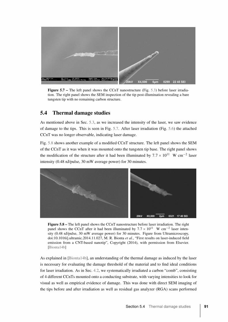
Figure 5.7 – The left panel shows the CCnT nanostructure (Fig. 5.3) before laser irradia-
tion. The right panel shows the SEM inspection of the tip post-illumination revealing a bare
tungsten tip with no remaining carbon structure.
5.4 Thermal damage studies
As mentioned above in Sec. 5.3, as we increased the intensity of the laser, we saw evidence
of damage to the tips. This is seen in Fig. 5.7. After laser irradiation (Fig. 5.6) the attached
CCnT was no longer observable, indicating laser damage.
Fig. 5.8 shows another example of a modified CCnT structure. The left panel shows the SEM
of the CCnT as it was when it was mounted onto the tungsten tip base. The right panel shows
the modification of the structure after it had been illuminated by 7.7ˆ 1011 W cm´2 laser
intensity (0.48 nJ/pulse, 30 mW average power) for 30 minutes.
Figure 5.8 – The left panel shows the CCnT nanostructure before laser irradiation. The right
panel shows the CCnT after it had been illuminated by 7.7ˆ 1011 W cm´2 laser inten-
sity (0.48 nJ/pulse, 30 mW average power) for 30 minutes. Figure from Ultramicroscopy,
doi:10.1016/j.ultramic.2014.11.027, M. R. Bionta et al., “First results on laser-induced field
emission from a CNT-based nanotip”, Copyright (2014), with permission from Elsevier.
[Bionta14b]
As explained in [Bionta14b], an understanding of the thermal damage as induced by the laser
is necessary for evaluating the damage threshold of the material and to find ideal conditions
for laser irradiation. As in Sec. 4.2, we systematically irradiated a carbon “comb”, consisting
of 4 different CCnTs mounted onto a conducting substrate, with varying intensities to look for
visual as well as empirical evidence of damage. This was done with direct SEM imaging of
the tips before and after irradiation as well as residual gas analyzer (RGA) scans performed
Section 5.4 Thermal damage studies 91
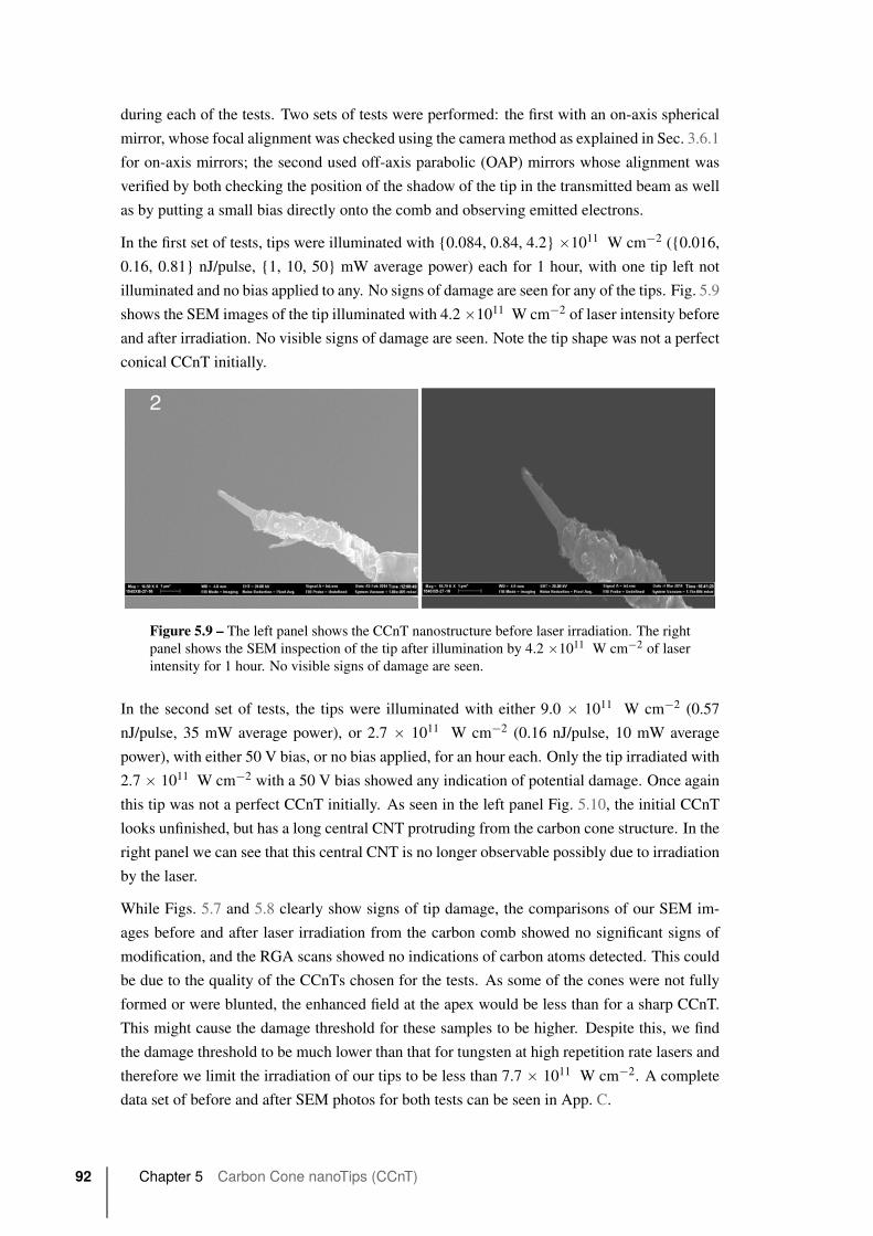
during each of the tests. Two sets of tests were performed: the first with an on-axis spherical
mirror, whose focal alignment was checked using the camera method as explained in Sec. 3.6.1
for on-axis mirrors; the second used off-axis parabolic (OAP) mirrors whose alignment was
verified by both checking the position of the shadow of the tip in the transmitted beam as well
as by putting a small bias directly onto the comb and observing emitted electrons.
In the first set of tests, tips were illuminated with {0.084, 0.84, 4.2} ˆ1011 W cm´2 ({0.016,
0.16, 0.81} nJ/pulse, {1, 10, 50} mW average power) each for 1 hour, with one tip left not
illuminated and no bias applied to any. No signs of damage are seen for any of the tips. Fig. 5.9
shows the SEM images of the tip illuminated with 4.2ˆ1011 W cm´2 of laser intensity before
and after irradiation. No visible signs of damage are seen. Note the tip shape was not a perfect
conical CCnT initially.
Figure 5.9 – The left panel shows the CCnT nanostructure before laser irradiation. The right
panel shows the SEM inspection of the tip after illumination by 4.2 ˆ1011 W cm´2 of laser
intensity for 1 hour. No visible signs of damage are seen.
In the second set of tests, the tips were illuminated with either 9.0 ˆ 1011 W cm´2 (0.57
nJ/pulse, 35 mW average power), or 2.7 ˆ 1011 W cm´2 (0.16 nJ/pulse, 10 mW average
power), with either 50 V bias, or no bias applied, for an hour each. Only the tip irradiated with
2.7 ˆ 1011 W cm´2 with a 50 V bias showed any indication of potential damage. Once again
this tip was not a perfect CCnT initially. As seen in the left panel Fig. 5.10, the initial CCnT
looks unfinished, but has a long central CNT protruding from the carbon cone structure. In the
right panel we can see that this central CNT is no longer observable possibly due to irradiation
by the laser.
While Figs. 5.7 and 5.8 clearly show signs of tip damage, the comparisons of our SEM im-
ages before and after laser irradiation from the carbon comb showed no significant signs of
modification, and the RGA scans showed no indications of carbon atoms detected. This could
be due to the quality of the CCnTs chosen for the tests. As some of the cones were not fully
formed or were blunted, the enhanced field at the apex would be less than for a sharp CCnT.
This might cause the damage threshold for these samples to be higher. Despite this, we find
the damage threshold to be much lower than that for tungsten at high repetition rate lasers and
therefore we limit the irradiation of our tips to be less than 7.7 ˆ 1011 W cm´2. A complete
data set of before and after SEM photos for both tests can be seen in App. C.
92 Chapter 5 Carbon Cone nanoTips (CCnT)
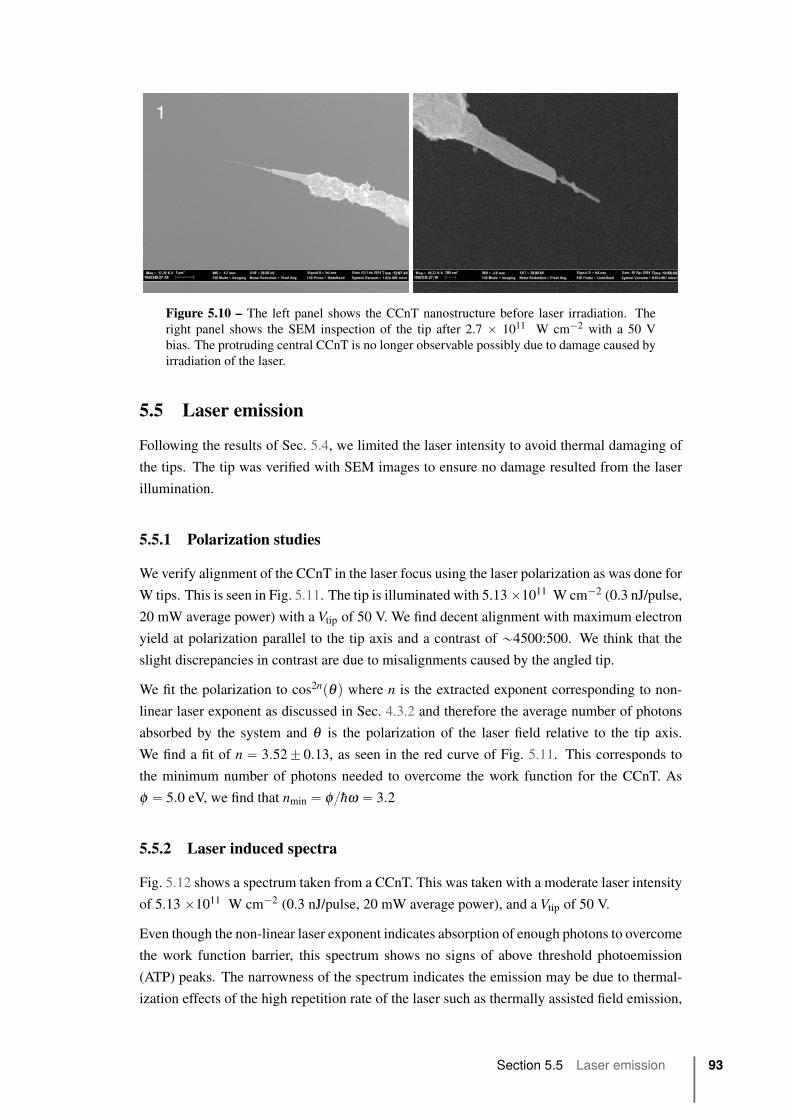
Figure 5.10 – The left panel shows the CCnT nanostructure before laser irradiation. The
right panel shows the SEM inspection of the tip after 2.7 ˆ 1011 W cm´2 with a 50 V
bias. The protruding central CCnT is no longer observable possibly due to damage caused by
irradiation of the laser.
5.5 Laser emission
Following the results of Sec. 5.4, we limited the laser intensity to avoid thermal damaging of
the tips. The tip was verified with SEM images to ensure no damage resulted from the laser
illumination.
5.5.1 Polarization studies
We verify alignment of the CCnT in the laser focus using the laser polarization as was done for
W tips. This is seen in Fig. 5.11. The tip is illuminated with 5.13ˆ1011 W cm´2 (0.3 nJ/pulse,
20 mW average power) with a Vtip of 50 V. We find decent alignment with maximum electron
yield at polarization parallel to the tip axis and a contrast of „4500:500. We think that the
slight discrepancies in contrast are due to misalignments caused by the angled tip.
We fit the polarization to cos2npθq where n is the extracted exponent corresponding to non-
linear laser exponent as discussed in Sec. 4.3.2 and therefore the average number of photons
absorbed by the system and θ is the polarization of the laser field relative to the tip axis.
We find a fit of n “ 3.52˘ 0.13, as seen in the red curve of Fig. 5.11. This corresponds to
the minimum number of photons needed to overcome the work function for the CCnT. As
φ “ 5.0 eV, we find that nmin “ φ{hω “ 3.2
5.5.2 Laser induced spectra
Fig. 5.12 shows a spectrum taken from a CCnT. This was taken with a moderate laser intensity
of 5.13 ˆ1011 W cm´2 (0.3 nJ/pulse, 20 mW average power), and a Vtip of 50 V.
Even though the non-linear laser exponent indicates absorption of enough photons to overcome
the work function barrier, this spectrum shows no signs of above threshold photoemission
(ATP) peaks. The narrowness of the spectrum indicates the emission may be due to thermal-
ization effects of the high repetition rate of the laser such as thermally assisted field emission,
Section 5.5 Laser emission 93
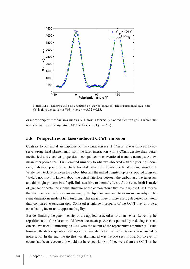
−90 0 90 1800
500
1000
1500
2000
2500
3000
3500
4000
4500
Polarization angle (θ)
Co
un
ts (
arb
. u.)
Vtip
= 100 V
cos2×3.5(θ)
Figure 5.11 – Electron yield as a function of laser polarization. The experimental data (blue
x’s) is fit to the curve cos2npθq where n“ 3.52˘0.13.
or more complex mechanisms such as ATP from a thermally excited electron gas in which the
temperature blurs the signature ATP peaks (i.e. if kBT „ hω).
5.6 Perspectives on laser-induced CCnT emission
Contrary to our initial assumptions on the characteristics of CCnTs, it was difficult to ob-
serve strong field phenomenon from the laser interaction with a CCnT, despite their better
mechanical and electrical properties in comparison to conventional metallic nanotips. At low
mean laser power, the CCnTs emitted similarly to what we observed with tungsten tips; how-
ever, high mean power proved to be harmful to the tips. Possible explanations are considered.
While the interface between the carbon fiber and the milled tungsten tip is a supposed tungsten
“weld”, not much is known about the actual interface between the carbon and the tungsten,
and this might prove to be a fragile link, sensitive to thermal effects. As the cone itself is made
of graphene sheets, the atomic structure of the carbon atoms that make up the CCnT means
that there are less carbon atoms making up the tip than compared to atoms in a nanotip of the
same dimensions made of bulk tungsten. This means there is more energy deposited per atom
than compared to tungsten tips. Some other unknown property of the CCnT may also be a
contributing factor to its apparent fragility.
Besides limiting the peak intensity of the applied laser, other solutions exist. Lowering the
repetition rate of the laser would lower the mean power thus potentially reducing thermal
effects. We tried illuminating a CCnT with the output of the regenerative amplifier at 1 kHz,
however the data acquisition settings at the time did not allow us to retrieve a good signal to
noise ratio. In the end, the tip that was illuminated was the one seen in Fig. 5.7 so even if
counts had been recovered, it would not have been known if they were from the CCnT or the
94 Chapter 5 Carbon Cone nanoTips (CCnT)
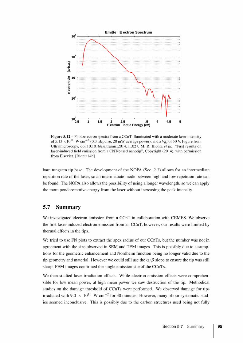
0.5 1 1.5 2 2.5 .5 4 4.5 5101
102
10
104
105
E ectron inetic Energy (eV)
eec
tron
yie
(arb
.u.)
Emitte E ectron Spectrum
Figure 5.12 – Photoelectron spectra from a CCnT illuminated with a moderate laser intensity
of 5.13ˆ1011 W cm´2 (0.3 nJ/pulse, 20 mW average power), and aVtip of 50 V. Figure from
Ultramicroscopy, doi:10.1016/j.ultramic.2014.11.027, M. R. Bionta et al., “First results on
laser-induced field emission from a CNT-based nanotip”, Copyright (2014), with permission
from Elsevier. [Bionta14b]
bare tungsten tip base. The development of the NOPA (Sec. 2.3) allows for an intermediate
repetition rate of the laser, so an intermediate mode between high and low repetition rate can
be found. The NOPA also allows the possibility of using a longer wavelength, so we can apply
the more ponderomotive energy from the laser without increasing the peak intensity.
5.7 Summary
We investigated electron emission from a CCnT in collaboration with CEMES. We observe
the first laser-induced electron emission from an CCnT; however, our results were limited by
thermal effects in the tips.
We tried to use FN plots to extract the apex radius of our CCnTs, but the number was not in
agreement with the size observed in SEM and TEM images. This is possibly due to assump-
tions for the geometric enhancement and Nordheim function being no longer valid due to the
tip geometry and material. However we could still use the α{β slope to ensure the tip was still
sharp. FEM images confirmed the single emission site of the CCnTs.
We then studied laser irradiation effects. While electron emission effects were comprehen-
sible for low mean power, at high mean power we saw destruction of the tip. Methodical
studies on the damage threshold of CCnTs were performed. We observed damage for tips
irradiated with 9.0 ˆ 1011 W cm´2 for 30 minutes. However, many of our systematic stud-
ies seemed inconclusive. This is possibly due to the carbon structures used being not fully
Section 5.7 Summary 95
formed or blunted, changing the enhancement. We limited our laser intensities to less than 7.7
ˆ 1011 W cm´2.
At low power, electron emission polarization dependency gave good contrast and a polariza-
tion fit of of n“ 3.4. This is in good agreement of the minimum number of photons absorbed
nmin “ 3.2 to overcome the φ “ 5 eV work function of the CCnT. Photoelectron spectra for
moderate intensity yielded a narrower spectra than those for similar intensities on tungsten,
indicating possible thermal effects. However, attempts at increasing the laser intensity to mea-
sure the yield as a function of laser power to extract an η proved to be unsuccessful as we
damaged the tip.
The development of a NOPA (Sec. 2.3) with variable repetition rate alongside our active col-
laboration with CEMES with the synthesis of CCnTs will hopefully lead to improved laser-
induced results. In particular the shape of the tip seems to be crucial towards maximizing the
emission process.
96 Chapter 5 Carbon Cone nanoTips (CCnT)
6Silver nanotip results
You were born a child of light’s wonderful secret— youreturn to the beauty you have always been.
– Aberjhani,
Visions of a Skylark Dressed in Black
In this chapter I detail results from silver nanotips. I was interested in using silver samples as
bulk silver has a known surface plasmon resonance around„400 nm, which is easily reachable
with our laser. I wanted to see how this resonance would affect electron emission and the
optical field enhancement. The resonance will be shifted by the behavior of the tip, and we
hope it will affect the electron emission in a measurable way. Studies on silver were done in
collaboration with GPM in Rouen.
I first briefly describe plasmonics and silver itself as a material. I then discuss the characteriza-
tion of our silver tips using SEM, FEM and FN techniques. Results taken at a high repetition
rate from the output of the oscillator are detailed, including results from a tip that did not
emit as expected. I describe results from low repetition rate which include the observance of
a spectral plateau as well as enhancement factor calculations. Finally, I present preliminary
results obtained with 400 nm laser irradiation.
6.1 Why silver?
Plasmonics describes a large field of physics which studies the interaction of electromagnetic
radiation with the free electrons in a noble metal [Enoch12, Maier07, Shahbazyan13]. What
happens is not evident, especially for sub-wavelength size metallic structures. At these sizes,
the electric field interacts with the conduction electrons at the interface of the metal leading
to an enhanced optical near field [Maier07]. This has brought the development of surface-
enhanced spectroscopy and applications of metamaterials and optical antennae.
The plasmon response of a nano-object is highly size and geometry dependent [Lee06, Mock02,
Vogel10, Ringe10]. In general sharp nanotips are used as local focusing elements for the plas-
mons [Babadjanyan00, Barthes12, Goncharenko07, Ma15, Vogelsang15]. In single material
tips, the apex is connected to a seemingly infinitely long shaft which supports the focusing
of the plasmons, however radiation effects reduce the enhancement factors in tips compared
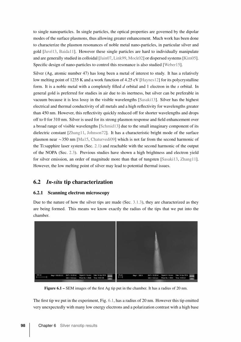
to single nanoparticles. In single particles, the optical properties are governed by the dipolar
modes of the surface plasmons, thus allowing greater enhancement. Much work has been done
to characterize the plasmon resonances of noble metal nano-particles, in particular silver and
gold [Juvé13, Baida11]. However these single particles are hard to individually manipulate
and are generally studied in colloidal [Jain07, Link99, Mock02] or dispersed systems [Kim05].
Specific design of nano-particles to control this resonance is also studied [Weber15].
Silver (Ag, atomic number 47) has long been a metal of interest to study. It has a relatively
low melting point of 1235 K and a work function of 4.25 eV [Haynes12] for its polycrystalline
form. It is a noble metal with a completely filled d orbital and 1 electron in the s orbital. In
general gold is preferred for studies in air due to its inertness, but silver can be preferable in
vacuum because it is less lossy in the visible wavelengths [Sasaki13]. Silver has the highest
electrical and thermal conductivity of all metals and a high reflectivity for wavelengths greater
than 450 nm. However, this reflectivity quickly reduced off for shorter wavelengths and drops
off to 0 for 310 nm. Silver is used for its strong plasmon response and field enhancement over
a broad range of visible wavelengths [Schmid13] due to the small imaginary component of its
dielectric constant [Zhang11, Johnson72]. It has a characteristic bright mode of the surface
plasmon near „350 nm [Ma15, Chaturvedi09] which is not far from the second harmonic of
the Ti:sapphire laser system (Sec. 2.1) and reachable with the second harmonic of the output
of the NOPA (Sec. 2.3). Previous studies have shown a high brightness and electron yield
for silver emission, an order of magnitude more than that of tungsten [Sasaki13, Zhang11].
However, the low melting point of silver may lead to potential thermal issues.
6.2 In-situ tip characterization
6.2.1 Scanning electron microscopy
Due to the nature of how the silver tips are made (Sec. 3.1.3), they are characterized as they
are being formed. This means we know exactly the radius of the tips that we put into the
chamber.
Figure 6.1 – SEM images of the first Ag tip put in the chamber. It has a radius of 20 nm.
The first tip we put in the experiment, Fig. 6.1, has a radius of 20 nm. However this tip emitted
very unexpectedly with many low energy electrons and a polarization contrast with a high base
98 Chapter 6 Silver nanotip results
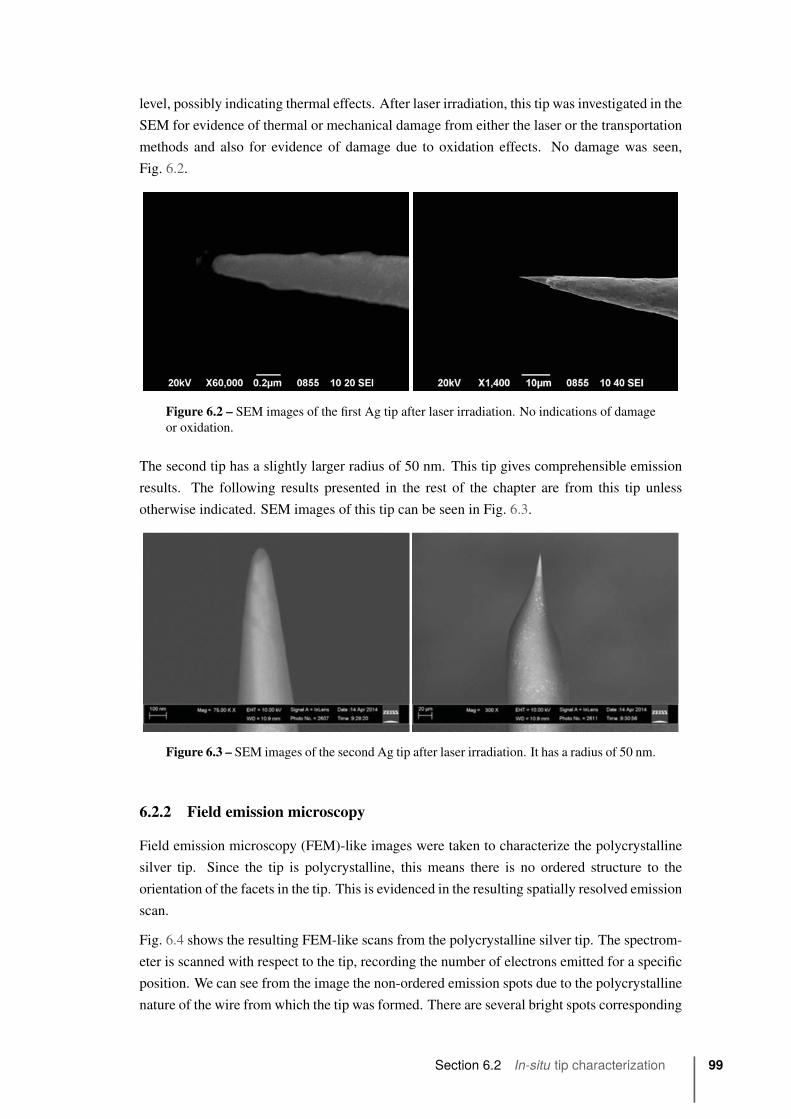
level, possibly indicating thermal effects. After laser irradiation, this tip was investigated in the
SEM for evidence of thermal or mechanical damage from either the laser or the transportation
methods and also for evidence of damage due to oxidation effects. No damage was seen,
Fig. 6.2.
Figure 6.2 – SEM images of the first Ag tip after laser irradiation. No indications of damage
or oxidation.
The second tip has a slightly larger radius of 50 nm. This tip gives comprehensible emission
results. The following results presented in the rest of the chapter are from this tip unless
otherwise indicated. SEM images of this tip can be seen in Fig. 6.3.
Figure 6.3 – SEM images of the second Ag tip after laser irradiation. It has a radius of 50 nm.
6.2.2 Field emission microscopy
Field emission microscopy (FEM)-like images were taken to characterize the polycrystalline
silver tip. Since the tip is polycrystalline, this means there is no ordered structure to the
orientation of the facets in the tip. This is evidenced in the resulting spatially resolved emission
scan.
Fig. 6.4 shows the resulting FEM-like scans from the polycrystalline silver tip. The spectrom-
eter is scanned with respect to the tip, recording the number of electrons emitted for a specific
position. We can see from the image the non-ordered emission spots due to the polycrystalline
nature of the wire from which the tip was formed. There are several bright spots corresponding
Section 6.2 In-situ tip characterization 99

Axis 1 (micron)
Axi
s 2
(mic
ron
)
2D Scan. Ag tip. Vtip = 1000 V. Vretard = 50 V
−4000 −2000 0 2000 4000 6000 8000−5000
−4000
−3000
−2000
−1000
0
1000
2000
3000
4000
5000
cou
nts
(lo
g s
cale
) (a
rb. u
.)
1
3
1E1
3E1
1E2
3E2
1E3
3E3
1E4
3E4
1E5
Figure 6.4 – FEM for a polycrystalline Ag tip. Since the wire from which the tip was formed
is polycrystalline, there is no ordered structure to the facet orientation of the tip.
to the many facets with the lowest work function (or bigger field enhancement) that we found
in our particular tip. These bright spots locations will change from tip to tip. We can position
the spectrometer such that it collects the highest brightness of emission using the FEM image
as a map.
The magnification of our FEM images is on the order of „ 106. This means that the bright
spot corresponds to an emission site size on the order of 1ˆ 1 nm2 in correspondence with
the emission site size seen in Sec. 5.2.3. The total emission area is on the order of 9ˆ6 nm2,
which is less than the measured radius and in accordance with expected emission size.
6.2.3 Fowler-Nordheim plots
Since we already know the size of the nanotip, Fowler-Nordheim (FN) plots were used to
periodically check the size of the tip to make sure that it is not destroyed.
Fig. 6.5 shows the ln`
1V 2
˘vs 1
V FN plot for the two brightly emitting facets seen in Fig. 6.4.
Facet 1 is the bright spot seen at (500, 5500) and has a α{β slope of 24080. Facet 2 is the
bright spot found at (-3500, 2000) and has an α{β slope of 23954. The slope of the two
facets is about the same indicating that their facet orientation is probably the same and that the
emission slope depends on the radius of the tip.
Since we have characterized the radius of the tip very well, we can use the FN equation to
verify the value of the Nordheim function vpwq. We know α as a function of vpwq and the
work function φ from Eq. 1.20, and that β “ 1{kr with k „ 5 and r given in Sec. 6.2.1. Using
r “ 50 nm, φ “ 4.26 eV, and the α{β slope given above, we find vpwq “ 0.6˘ 0.02. Even
though the tip shape is not exactly the same, and material are different than in Sec. 4.1.1, our
100 Chapter 6 Silver nanotip results
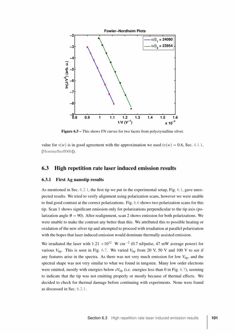
0.8 0.9 1 1.1 1.2 1.3 1.4 1.5 1.6
x 10−3
−9
−8
−7
−6
−5
−4
−3
−2
1/V (V−1)
ln(J
/V2 )
(arb
. u.)
Fowler−Nordheim Plots
α/β1 = 24080
α/β2 = 23954
Figure 6.5 – This shows FN curves for two facets from polycrystalline silver.
value for vpwq is in good agreement with the approximation we used (vpwq “ 0.6, Sec. 4.1.1,
[Hommelhoff06b]).
6.3 High repetition rate laser induced emission results
6.3.1 First Ag nanotip results
As mentioned in Sec. 6.2.1, the first tip we put in the experimental setup, Fig. 6.1, gave unex-
pected results. We tried to verify alignment using polarization scans, however we were unable
to find good contrast at the correct polarizations. Fig. 6.6 shows two polarization scans for this
tip. Scan 1 shows significant emission only for polarizations perpendicular to the tip axis (po-
larization angle θ “ 90). After realignment, scan 2 shows emission for both polarizations. We
were unable to make the contrast any better than this. We attributed this to possible heating or
oxidation of the new silver tip and attempted to proceed with irradiation at parallel polarization
with the hopes that laser induced emission would dominate thermally assisted emission.
We irradiated the laser with 1.21 ˆ1012 W cm´2 (0.7 nJ/pulse, 47 mW average power) for
various Vtip. This is seen in Fig. 6.7. We varied Vtip from 20 V, 50 V and 100 V to see if
any features arise in the spectra. As there was not very much emission for low Vtip, and the
spectral shape was not very similar to what we found in tungsten. Many low order electrons
were emitted, mostly with energies below eVtip (i.e. energies less than 0 in Fig. 6.7), seeming
to indicate that the tip was not emitting properly or mostly because of thermal effects. We
decided to check for thermal damage before continuing with experiments. None were found
as discussed in Sec. 6.2.1.
Section 6.3 High repetition rate laser induced emission results 101
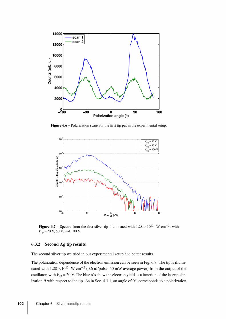
−180 −90 0 90 1800
2000
4000
6000
8000
10000
12000
14000
Polarization angle (θ)
Co
un
ts (
arb
. u.)
scan 1scan 2
Figure 6.6 – Polarization scans for the first tip put in the experimental setup.
−5 0 5 10 1510
1
102
103
104
105
106
Energy (eV)
co
un
ts -
- lo
g s
ca
le (
arb
. u
.)
Vtip
= 20 V
Vtip
= 50 V
Vtip
= 100 V
Figure 6.7 – Spectra from the first silver tip illuminated with 1.28 ˆ1012 W cm´2, with
Vtip =20 V, 50 V, and 100 V.
6.3.2 Second Ag tip results
The second silver tip we tried in our experimental setup had better results.
The polarization dependence of the electron emission can be seen in Fig. 6.8. The tip is illumi-
nated with 1.28 ˆ1012 W cm´2 (0.6 nJ/pulse, 50 mW average power) from the output of the
oscillator, withVtip = 20 V. The blue x’s show the electron yield as a function of the laser polar-
ization θ with respect to the tip. As in Sec. 4.3.1, an angle of 0˝ corresponds to a polarization
102 Chapter 6 Silver nanotip results
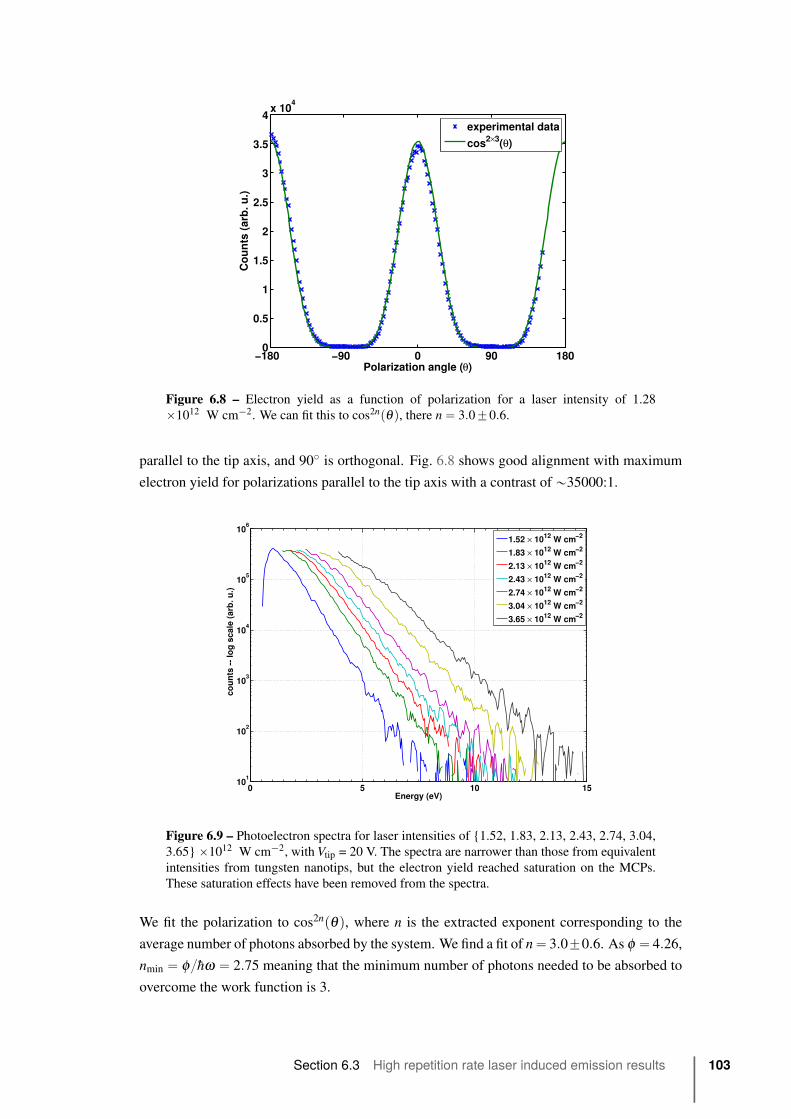
−180 −90 0 90 1800
0.5
1
1.5
2
2.5
3
3.5
4x 10
4
Polarization angle (θ)
Co
un
ts (
arb
. u.)
experimental data
cos2×3(θ)
Figure 6.8 – Electron yield as a function of polarization for a laser intensity of 1.28
ˆ1012 W cm´2. We can fit this to cos2npθq, there n“ 3.0˘0.6.
parallel to the tip axis, and 90˝ is orthogonal. Fig. 6.8 shows good alignment with maximum
electron yield for polarizations parallel to the tip axis with a contrast of „35000:1.
0 5 10 1510
1
102
103
104
105
106
Energy (eV)
co
un
ts -
- lo
g s
ca
le (
arb
. u
.)
1.52 × 10¹²
W cm−2
1.83 × 10¹²
W cm−2
2.13 × 10¹²
W cm−2
2.43 × 10¹²
W cm−2
2.74 × 10¹²
W cm−2
3.04 × 10¹²
W cm−2
3.65 × 10¹²
W cm−2
Figure 6.9 – Photoelectron spectra for laser intensities of {1.52, 1.83, 2.13, 2.43, 2.74, 3.04,
3.65} ˆ1012 W cm´2, with Vtip = 20 V. The spectra are narrower than those from equivalent
intensities from tungsten nanotips, but the electron yield reached saturation on the MCPs.
These saturation effects have been removed from the spectra.
We fit the polarization to cos2npθq, where n is the extracted exponent corresponding to the
average number of photons absorbed by the system. We find a fit of n“ 3.0˘0.6. As φ “ 4.26,
nmin “ φ{hω “ 2.75 meaning that the minimum number of photons needed to be absorbed to
overcome the work function is 3.
Section 6.3 High repetition rate laser induced emission results 103
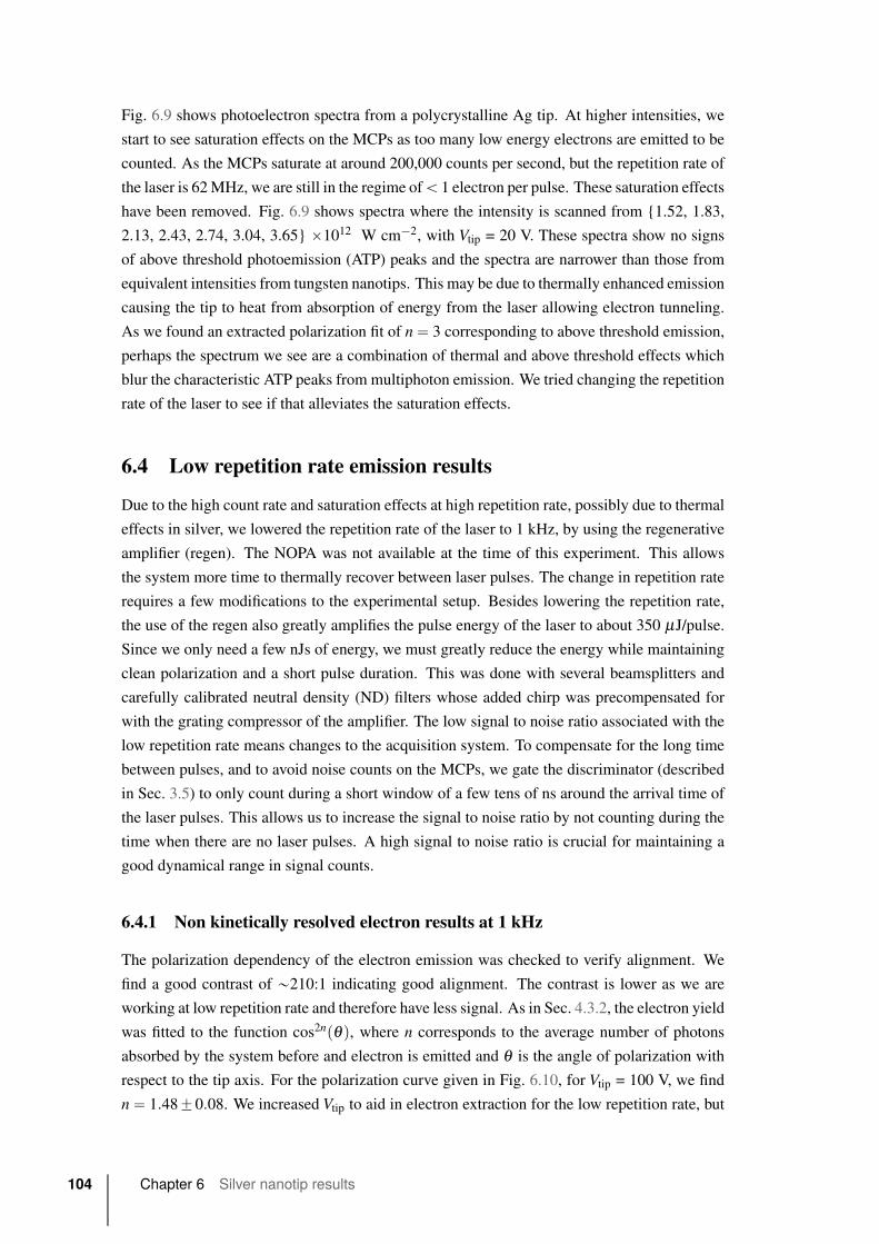
Fig. 6.9 shows photoelectron spectra from a polycrystalline Ag tip. At higher intensities, we
start to see saturation effects on the MCPs as too many low energy electrons are emitted to be
counted. As the MCPs saturate at around 200,000 counts per second, but the repetition rate of
the laser is 62MHz, we are still in the regime ofă 1 electron per pulse. These saturation effects
have been removed. Fig. 6.9 shows spectra where the intensity is scanned from {1.52, 1.83,
2.13, 2.43, 2.74, 3.04, 3.65} ˆ1012 W cm´2, with Vtip = 20 V. These spectra show no signs
of above threshold photoemission (ATP) peaks and the spectra are narrower than those from
equivalent intensities from tungsten nanotips. This may be due to thermally enhanced emission
causing the tip to heat from absorption of energy from the laser allowing electron tunneling.
As we found an extracted polarization fit of n“ 3 corresponding to above threshold emission,
perhaps the spectrum we see are a combination of thermal and above threshold effects which
blur the characteristic ATP peaks from multiphoton emission. We tried changing the repetition
rate of the laser to see if that alleviates the saturation effects.
6.4 Low repetition rate emission results
Due to the high count rate and saturation effects at high repetition rate, possibly due to thermal
effects in silver, we lowered the repetition rate of the laser to 1 kHz, by using the regenerative
amplifier (regen). The NOPA was not available at the time of this experiment. This allows
the system more time to thermally recover between laser pulses. The change in repetition rate
requires a few modifications to the experimental setup. Besides lowering the repetition rate,
the use of the regen also greatly amplifies the pulse energy of the laser to about 350 μJ/pulse.
Since we only need a few nJs of energy, we must greatly reduce the energy while maintaining
clean polarization and a short pulse duration. This was done with several beamsplitters and
carefully calibrated neutral density (ND) filters whose added chirp was precompensated for
with the grating compressor of the amplifier. The low signal to noise ratio associated with the
low repetition rate means changes to the acquisition system. To compensate for the long time
between pulses, and to avoid noise counts on the MCPs, we gate the discriminator (described
in Sec. 3.5) to only count during a short window of a few tens of ns around the arrival time of
the laser pulses. This allows us to increase the signal to noise ratio by not counting during the
time when there are no laser pulses. A high signal to noise ratio is crucial for maintaining a
good dynamical range in signal counts.
6.4.1 Non kinetically resolved electron results at 1 kHz
The polarization dependency of the electron emission was checked to verify alignment. We
find a good contrast of „210:1 indicating good alignment. The contrast is lower as we are
working at low repetition rate and therefore have less signal. As in Sec. 4.3.2, the electron yield
was fitted to the function cos2npθq, where n corresponds to the average number of photons
absorbed by the system before and electron is emitted and θ is the angle of polarization with
respect to the tip axis. For the polarization curve given in Fig. 6.10, for Vtip = 100 V, we find
n“ 1.48˘0.08. We increased Vtip to aid in electron extraction for the low repetition rate, but
104 Chapter 6 Silver nanotip results
kept it low enough as to not significantly reduce the resolution of the spectrometer and impact
the effective work function of the tip. This number is much less than the nmin, the minimum
number of photons needed to be absorbed to overcome the work function for polycrystalline
silver. As discussed above, the work function φ “ 4.26 eV for polycrystalline silver, this
means that for a photon energy of 1.55 eV for 800 nm light, φ{hω “ 2.75 which is larger than
the extracted n.
−180 −90 0 90 1800
50
100
150
200
250
Polarization angle (θ)
Co
un
ts (
arb
. u.)
Vtip
= 100 V
cos2×1.48(θ)
Figure 6.10 – Electron yield as a function of laser polarization (θ ) with respect to the tip
axis. The experimental data (blue x’s) are fit with the form cos2n where n“ 1.48˘0.08.
Laser power dependent curves, Fig 6.11, were also used to approximate η from J 9 Iη . Here,
the laser intensity was scanned from 0.92 to 21.0 ˆ 1012 W cm´2 (6.2 nJ to 14.8 nJ), for
Vtip = 50 V. Fig 6.11 (a) shows the electron yield as a function of intensity. Plotting this yield
in log-log scale, Fig 6.11 (b), we can fit a linear relation with a slope, and extracted exponent,
of η “ 1.84˘0.84.
There could be many reasons for such a low extracted n and η . The laser intensity range is lim-
ited by experimental constraints, so the fit is done on a quite narrow range. Geometric effects
would also skew the effects. As the repetition rate of the laser is 1 kHz, the maximum number
of electrons we can count with the MCPs is 1000 per second. We count a high number of
electrons detected by the MCPs (up to „500 counts / second). Taking into account the trans-
mission of the spectrometer, and the pinhole entrance to the spectrometer, there could have
been more than one electron emitted per pulse. Space charge effects would cause Coulomb
repulsion between the electrons meaning less electrons would be detected. This would cause
the maximum of the polarization curve to be lower and the extracted exponent to be lower,
but would not affect the resolution of kinetically resolved spectra. Photofield and thermally
enhanced emission are all emission mechanisms that occur after absorption of less than nmin
Section 6.4 Low repetition rate emission results 105

4 5 6 7 8 9 10 11
x 1011
200
300
400
500
600
700
800
900
1000
1100
1200
laser intensity (W cm−2)
cou
nts
(ar
b .u
.)
Laser Power Scans(a)
26.8 27 27.2 27.4 27.6 27.85.4
5.6
5.8
6
6.2
6.4
6.6
6.8
7
7.2
log(laser intensity)
log
(co
un
ts)
(arb
.u
.)
Laser Power Scans
data
fit
(b)
Figure 6.11 – (a) This shows the electron yield as a function of laser power for Vtip = 50 V.
(b) This shows the same yield on a log-log scale. We can fit this curve to a linear equation
from which the slope η “ 1.84˘0.84.
photons. In order to better understand the physical mechanisms behind the observed emission,
we investigated the kinetically resolved photoelectron spectra.
6.4.2 Kinetically resolved analysis at 1 kHz
We take the kinetically resolved electron spectra to see if, by spectral shape, we can identify
the regime of the electron emission. The spectra can be seen in Fig. 6.12 for a range of laser
intensities.
�� �� �� �� �� �����
���
���
�� ������ ���
���
������� ���������������
�������������� �
�������������� �
�������������� �
�������������� �
��������'����
������
���''����
Figure 6.12 – Photoelectron spectra for laser intensities of {0.918, 12.4, 16.3, 21.0}
ˆ1012 W cm´2, Vtip = 50 V. Note the observance of a spectral plateau.
The spectra we record have distinct regions. The lower energy electrons show the characteristic
exponential decay of above threshold photoemission. For higher intensities, a spectral plateau
builds up for high energy electrons, where the count rate remains almost the same. This
106 Chapter 6 Silver nanotip results
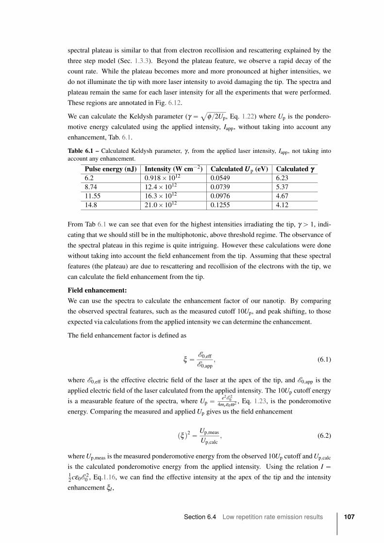
spectral plateau is similar to that from electron recollision and rescattering explained by the
three step model (Sec. 1.3.3). Beyond the plateau feature, we observe a rapid decay of the
count rate. While the plateau becomes more and more pronounced at higher intensities, we
do not illuminate the tip with more laser intensity to avoid damaging the tip. The spectra and
plateau remain the same for each laser intensity for all the experiments that were performed.
These regions are annotated in Fig. 6.12.
We can calculate the Keldysh parameter (γ “aφ{2Up, Eq. 1.22) where Up is the pondero-
motive energy calculated using the applied intensity, Iapp, without taking into account any
enhancement, Tab. 6.1.
Table 6.1 – Calculated Keldysh parameter, γ , from the applied laser intensity, Iapp, not taking into
account any enhancement.
Pulse energy (nJ) Intensity (W cm´2) Calculated UUUp (eV) Calculated γγγ6.2 0.918ˆ1012 0.0549 6.23
8.74 12.4ˆ1012 0.0739 5.37
11.55 16.3ˆ1012 0.0976 4.67
14.8 21.0ˆ1012 0.1255 4.12
From Tab 6.1 we can see that even for the highest intensities irradiating the tip, γ ą 1, indi-
cating that we should still be in the multiphotonic, above threshold regime. The observance of
the spectral plateau in this regime is quite intriguing. However these calculations were done
without taking into account the field enhancement from the tip. Assuming that these spectral
features (the plateau) are due to rescattering and recollision of the electrons with the tip, we
can calculate the field enhancement from the tip.
Field enhancement:We can use the spectra to calculate the enhancement factor of our nanotip. By comparing
the observed spectral features, such as the measured cutoff 10Up, and peak shifting, to those
expected via calculations from the applied intensity we can determine the enhancement.
The field enhancement factor is defined as
ξ “ E0,eff
E0,app, (6.1)
where E0,eff is the effective electric field of the laser at the apex of the tip, and E0,app is the
applied electric field of the laser calculated from the applied intensity. The 10Up cutoff energy
is a measurable feature of the spectra, where Up “ e2E 20
4meε0ω2 , Eq. 1.23, is the ponderomotive
energy. Comparing the measured and applied Up gives us the field enhancement
pξ q2 “ Up,meas
Up,calc, (6.2)
whereUp,meas is the measured ponderomotive energy from the observed 10Up cutoff andUp,calc
is the calculated ponderomotive energy from the applied intensity. Using the relation I “12cε0E 2
0 , Eq.1.16, we can find the effective intensity at the apex of the tip and the intensity
enhancement ξI ,
Section 6.4 Low repetition rate emission results 107

pξ q2 “ ξI. (6.3)
In practice, we use the measured and calculated ponderomotive energy to calculate the inten-
sity enhancement which in turn is used to calculated the field enhancement.
Peak shifting:We observe a peak shifting effect for the low-order spectral features which become more pro-
nounced as the intensity increases. This causes the spectral features to shift to lower energy.
This is attributed to the channel closing effect (Sec. 1.3.2). At high intensity, the ponderomo-
tive energy, Up, of the photoelectron is not negligible. This energy is added in addition to the
energy difference of the final and initial states of the photoelectron. This means that there is an
energy shift ΔE for all spectral features, where ΔE “´Up. We can use this to calculate Up for
the photoelectrons. As we add a potential Vtip to the tip to extract the electrons, the energy of
the first peak should be,
Epeak1 “ nhω´φ ´Up´ eVtip, (6.4)
where n is the minimum number of photons needed to be absorbed to overcome the work
function, in this case 3. By comparing this measured Up, to the Up calculated from the applied
laser intensity, we can extract an intensity enhancement factor: ξI “Up,meas{Up,calc, showin in
Tab. 6.2.
Table 6.2 – Calculated Up and intensity enhancement factor, ξI , using the measured Up from peak
shifting.
Pulse Intensity Calculated First peak Measuredenergy (nJ) (W cm´2) UUUp (eV) location (eV) UUUp (eV) ξξξ III6.2 0.918ˆ1012 0.0549 50.1 0.29 5.28
8.74 12.4ˆ1012 0.0739 49.7 0.69 9.34
11.55 16.3ˆ1012 0.0976 49.3 1.09 11.2
14.8 21.0ˆ1012 0.1255 48.6 1.79 14.3
We can now correct the kinetic energy axis of Fig. 6.12 by shifting the spectra by Up + eVtip.
This is seen in Fig. 6.13.
Cutoff energy:As spectral shifting can also be cause by other effects apart from channel closing, such as
geometric effects from angled tips, we compare our results to other methods of determining
Up. As discussed in Sec. 1.3.3, we assume that the maximum final energy an electron can gain
through rescattering is 10Up. This assumption is a theoretical expansion upon calculations and
observations from atomic systems [Krüger12b]. We determine the 10Up cutoff from dropoff
in the plateau in the spectra for higher energy electrons as in [Krüger12b], thus experimentally
identifying the 10Up cutoff energy, Ecut.
We fit a straight line to the plateau of the spectra and a straight line to the drop off in energy
for higher energy electrons. The intersection of these two fits is considered the 10Up cutoff, as
108 Chapter 6 Silver nanotip results
� � �� �� �����
���
���
���������
� ��������� ����������������
�������������� �
������������� �
�������������� �
�������������� �
Figure 6.13 – Photoelectron spectra from Fig. 6.12 measured relative to the Fermi energy,
eVtip + Up (from Tab. 6.2). The energy cutoff energy can be determined by the dropoff from
the plateau at the for the higher energy electrons.
seen in Fig. 6.13. This is a similar methodology as is done in [Krüger12b]. From the measured
cutoff and therefore measured Up, we can compare the values to the calculated Up based on
the applied intensity to find a value for the intensity and field enhancements which we can
compare to the value from above. We can use the intensity enhancement factor to calculated
the effective Keldysh parameter from the effective intensity, Ieff.
Table 6.3 – The measured cutoff energy from Fig. 6.12 and intensity enhancement ξI with correspond-
ing effective intensity and Keldysh parameter γ .
Pulse Applied Effectiveenergy intensity Calculated Measured intensity Effective(nJ) (W cm´2) cutoff (eV) cutoff (eV) ξξξ III (W cm´2) γγγ6.2 0.918ˆ1012 0.549 5.4 9.84 0.90ˆ1013 1.99
8.74 12.4ˆ1012 0.739 8.1 11.0 1.36ˆ1013 1.62
11.55 16.3ˆ1012 0.976 11.6 11.9 1.94ˆ1013 1.36
14.8 21.0ˆ1012 1.255 15.8 12.6 2.64ˆ1013 1.16
We see that with the calculated enhancement factor γ „ 1 indicating a transition into the optical
tunneling regime. This is in good agreement with the appearance of a spectral plateau.
The measured cutoff should scale linearly with the effective intensity. Indeed it does as seen
in Fig. 6.14. The intensity dependence of the cutoff with the applied intensity yields a linear
scaling with a slope of 8.81 ˘ 0.07 eV/(1012 W cm´2) and an offset of 2.74 ˘ 0.52 eV seen
in the blue line in Fig. 6.14. As Ecut 9 Ieff, there should not be an offset in the fit. This
offset can be attributed to geometric factors in the experimental setup such as a tilted tip
with respect to the spectrometer, thus shifting the effective Fermi level or a systematic error
in our assumption of the Fermi level. We can correct for this error by shifting the spectra
by the offset. The corrected spectra can be seen in Fig. 6.15. This yields a new measured
Section 6.4 Low repetition rate emission results 109
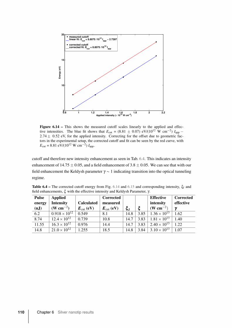
0.8 1 1.2 1.4 1.6 1.8 2 2.25
10
15
20
Applied intensity (× 1012 W cm−2)
En
erg
y (e
V)
measured cutofflinear fit: E
cut = 8.8075 /1012 I
app − 2.7397
corrected cutoffcorrected fit: E
cut = 8.8075 /1012 I
app
Figure 6.14 – This shows the measured cutoff scales linearly to the applied and effec-
tive intensities. The blue fit shows that Ecut = (8.81 ˘ 0.07) eV/(1012 W cm´2) Iapp ´2.74˘ 0.52 eV, for the applied intensity. Correcting for the offset due to geometric fac-
tors in the experimental setup, the corrected cutoff and fit can be seen by the red curve, with
Ecut = 8.81 eV/(1012 W cm´2) Iapp.
cutoff and therefore new intensity enhancement as seen in Tab. 6.4. This indicates an intensity
enhancement of 14.75˘ 0.05, and a field enhancement of 3.8˘ 0.05. We can see that with our
field enhancement the Keldysh parameter γ „ 1 indicating transition into the optical tunneling
regime.
Table 6.4 – The corrected cutoff energy from Fig. 6.14 and 6.15 and corresponding intensity, ξI and
field enhancements, ξ with the effective intensity and Keldysh Parameter, γ .
Pulse Applied Corrected Effective Correctedenergy Intensity Calculated measured intensity effective(nJ) (W cm´2) EEEcut (eV) EEEcut (eV) ξξξ III ξξξ (W cm´2q γγγ6.2 0.918ˆ1012 0.549 8.1 14.8 3.85 1.36ˆ1013 1.62
8.74 12.4ˆ1012 0.739 10.8 14.7 3.83 1.81ˆ1013 1.40
11.55 16.3ˆ1012 0.976 14.4 14.7 3.83 2.40ˆ1013 1.22
14.8 21.0ˆ1012 1.255 18.5 14.8 3.84 3.10ˆ1013 1.07
110 Chapter 6 Silver nanotip results
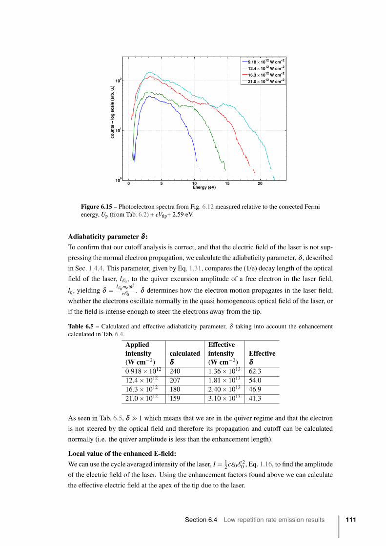
0 5 10 15 2010
0
101
102
Energy (eV)
co
un
ts -
- lo
g s
ca
le (
arb
. u
.)
9.18 × 10¹²
W cm−2
12.4 × 10¹²
W cm−2
16.3 × 10¹²
W cm−2
21.0 × 10¹²
W cm−2
Figure 6.15 – Photoelectron spectra from Fig. 6.12 measured relative to the corrected Fermi
energy, Up (from Tab. 6.2) + eVtip+ 2.59 eV.
Adiabaticity parameter δδδ :To confirm that our cutoff analysis is correct, and that the electric field of the laser is not sup-
pressing the normal electron propagation, we calculate the adiabaticity parameter, δ , describedin Sec. 1.4.4. This parameter, given by Eq. 1.31, compares the (1/e) decay length of the optical
field of the laser, lE0, to the quiver excursion amplitude of a free electron in the laser field,
lq, yielding δ “ lE0meω2
eE0. δ determines how the electron motion propagates in the laser field,
whether the electrons oscillate normally in the quasi homogeneous optical field of the laser, or
if the field is intense enough to steer the electrons away from the tip.
Table 6.5 – Calculated and effective adiabaticity parameter, δ taking into account the enhancement
calculated in Tab. 6.4.
Applied Effectiveintensity calculated intensity Effective(W cm´2) δδδ (W cm´2) δδδ0.918ˆ1012 240 1.36ˆ1013 62.3
12.4ˆ1012 207 1.81ˆ1013 54.0
16.3ˆ1012 180 2.40ˆ1013 46.9
21.0ˆ1012 159 3.10ˆ1013 41.3
As seen in Tab. 6.5, δ " 1 which means that we are in the quiver regime and that the electron
is not steered by the optical field and therefore its propagation and cutoff can be calculated
normally (i.e. the quiver amplitude is less than the enhancement length).
Local value of the enhanced E-field:We can use the cycle averaged intensity of the laser, I“ 1
2cε0E 2
0 , Eq. 1.16, to find the amplitude
of the electric field of the laser. Using the enhancement factors found above we can calculate
the effective electric field at the apex of the tip due to the laser.
Section 6.4 Low repetition rate emission results 111
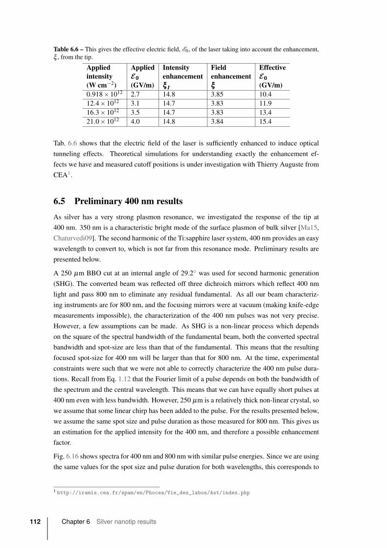
Table 6.6 – This gives the effective electric field, E0, of the laser taking into account the enhancement,
ξ , from the tip.
Applied Applied Intensity Field Effectiveintensity E000 enhancement enhancement E000
(W cm´2) (GV/m) ξξξ III ξξξ (GV/m)0.918ˆ1012 2.7 14.8 3.85 10.4
12.4ˆ1012 3.1 14.7 3.83 11.9
16.3ˆ1012 3.5 14.7 3.83 13.4
21.0ˆ1012 4.0 14.8 3.84 15.4
Tab. 6.6 shows that the electric field of the laser is sufficiently enhanced to induce optical
tunneling effects. Theoretical simulations for understanding exactly the enhancement ef-
fects we have and measured cutoff positions is under investigation with Thierry Auguste from
CEA1.
6.5 Preliminary 400 nm resultsAs silver has a very strong plasmon resonance, we investigated the response of the tip at
400 nm. 350 nm is a characteristic bright mode of the surface plasmon of bulk silver [Ma15,
Chaturvedi09]. The second harmonic of the Ti:sapphire laser system, 400 nm provides an easy
wavelength to convert to, which is not far from this resonance mode. Preliminary results are
presented below.
A 250 μm BBO cut at an internal angle of 29.2˝ was used for second harmonic generation
(SHG). The converted beam was reflected off three dichroich mirrors which reflect 400 nm
light and pass 800 nm to eliminate any residual fundamental. As all our beam characteriz-
ing instruments are for 800 nm, and the focusing mirrors were at vacuum (making knife-edge
measurements impossible), the characterization of the 400 nm pulses was not very precise.
However, a few assumptions can be made. As SHG is a non-linear process which depends
on the square of the spectral bandwidth of the fundamental beam, both the converted spectral
bandwidth and spot-size are less than that of the fundamental. This means that the resulting
focused spot-size for 400 nm will be larger than that for 800 nm. At the time, experimental
constraints were such that we were not able to correctly characterize the 400 nm pulse dura-
tions. Recall from Eq. 1.12 that the Fourier limit of a pulse depends on both the bandwidth of
the spectrum and the central wavelength. This means that we can have equally short pulses at
400 nm even with less bandwidth. However, 250 μm is a relatively thick non-linear crystal, so
we assume that some linear chirp has been added to the pulse. For the results presented below,
we assume the same spot size and pulse duration as those measured for 800 nm. This gives us
an estimation for the applied intensity for the 400 nm, and therefore a possible enhancement
factor.
Fig. 6.16 shows spectra for 400 nm and 800 nm with similar pulse energies. Since we are using
the same values for the spot size and pulse duration for both wavelengths, this corresponds to
1 http://iramis.cea.fr/spam/en/Phocea/Vie_des_labos/Ast/index.php
112 Chapter 6 Silver nanotip results
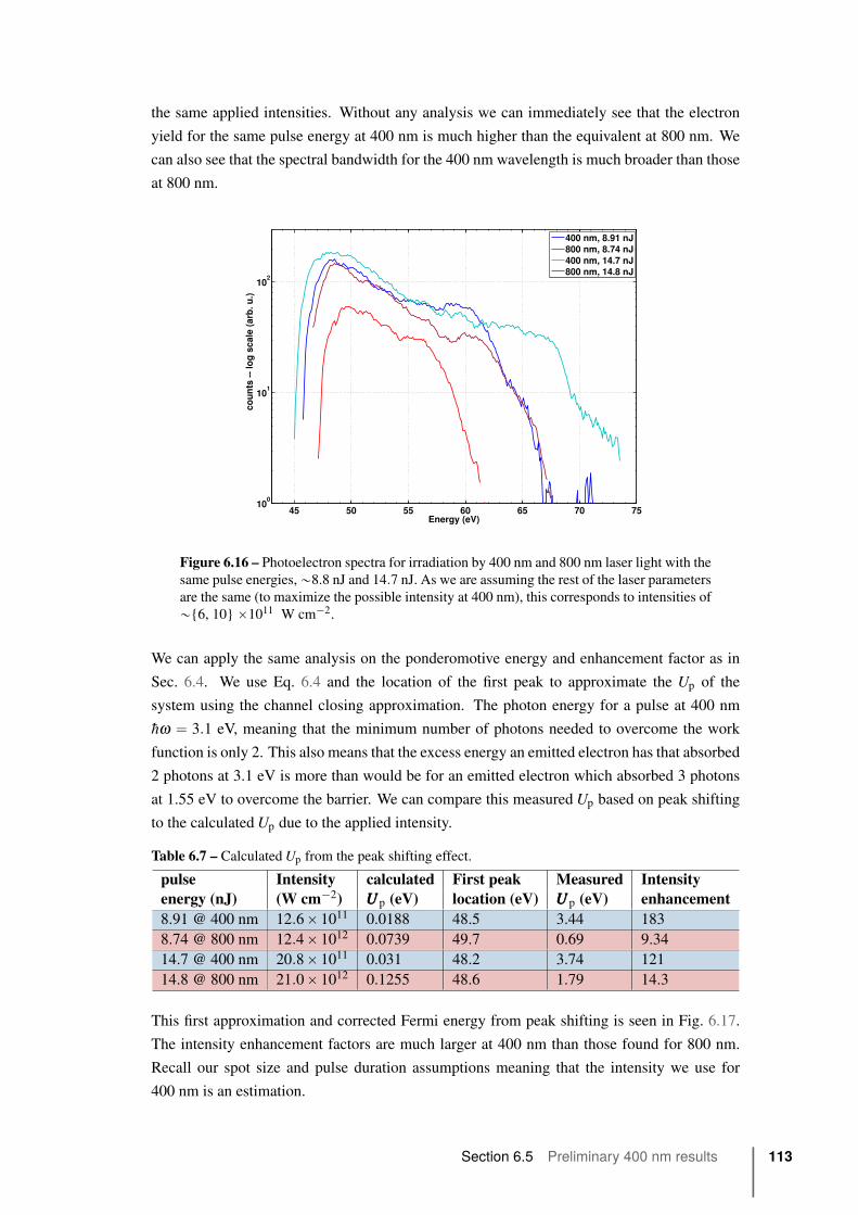
the same applied intensities. Without any analysis we can immediately see that the electron
yield for the same pulse energy at 400 nm is much higher than the equivalent at 800 nm. We
can also see that the spectral bandwidth for the 400 nm wavelength is much broader than those
at 800 nm.
45 50 55 60 65 70 7510
0
101
102
Energy (eV)
co
un
ts -
- lo
g s
ca
le (
arb
. u
.)400 nm, 8.91 nJ
800 nm, 8.74 nJ
400 nm, 14.7 nJ
800 nm, 14.8 nJ
Figure 6.16 – Photoelectron spectra for irradiation by 400 nm and 800 nm laser light with the
same pulse energies,„8.8 nJ and 14.7 nJ. As we are assuming the rest of the laser parameters
are the same (to maximize the possible intensity at 400 nm), this corresponds to intensities of
„{6, 10} ˆ1011 W cm´2.
We can apply the same analysis on the ponderomotive energy and enhancement factor as in
Sec. 6.4. We use Eq. 6.4 and the location of the first peak to approximate the Up of the
system using the channel closing approximation. The photon energy for a pulse at 400 nm
hω “ 3.1 eV, meaning that the minimum number of photons needed to overcome the work
function is only 2. This also means that the excess energy an emitted electron has that absorbed
2 photons at 3.1 eV is more than would be for an emitted electron which absorbed 3 photons
at 1.55 eV to overcome the barrier. We can compare this measured Up based on peak shifting
to the calculated Up due to the applied intensity.
Table 6.7 – Calculated Up from the peak shifting effect.
pulse Intensity calculated First peak Measured Intensityenergy (nJ) (W cm´2) UUUp (eV) location (eV) UUUp (eV) enhancement8.91 @ 400 nm 12.6ˆ1011 0.0188 48.5 3.44 183
8.74 @ 800 nm 12.4ˆ1012 0.0739 49.7 0.69 9.34
14.7 @ 400 nm 20.8ˆ1011 0.031 48.2 3.74 121
14.8 @ 800 nm 21.0ˆ1012 0.1255 48.6 1.79 14.3
This first approximation and corrected Fermi energy from peak shifting is seen in Fig. 6.17.
The intensity enhancement factors are much larger at 400 nm than those found for 800 nm.
Recall our spot size and pulse duration assumptions meaning that the intensity we use for
400 nm is an estimation.
Section 6.5 Preliminary 400 nm results 113
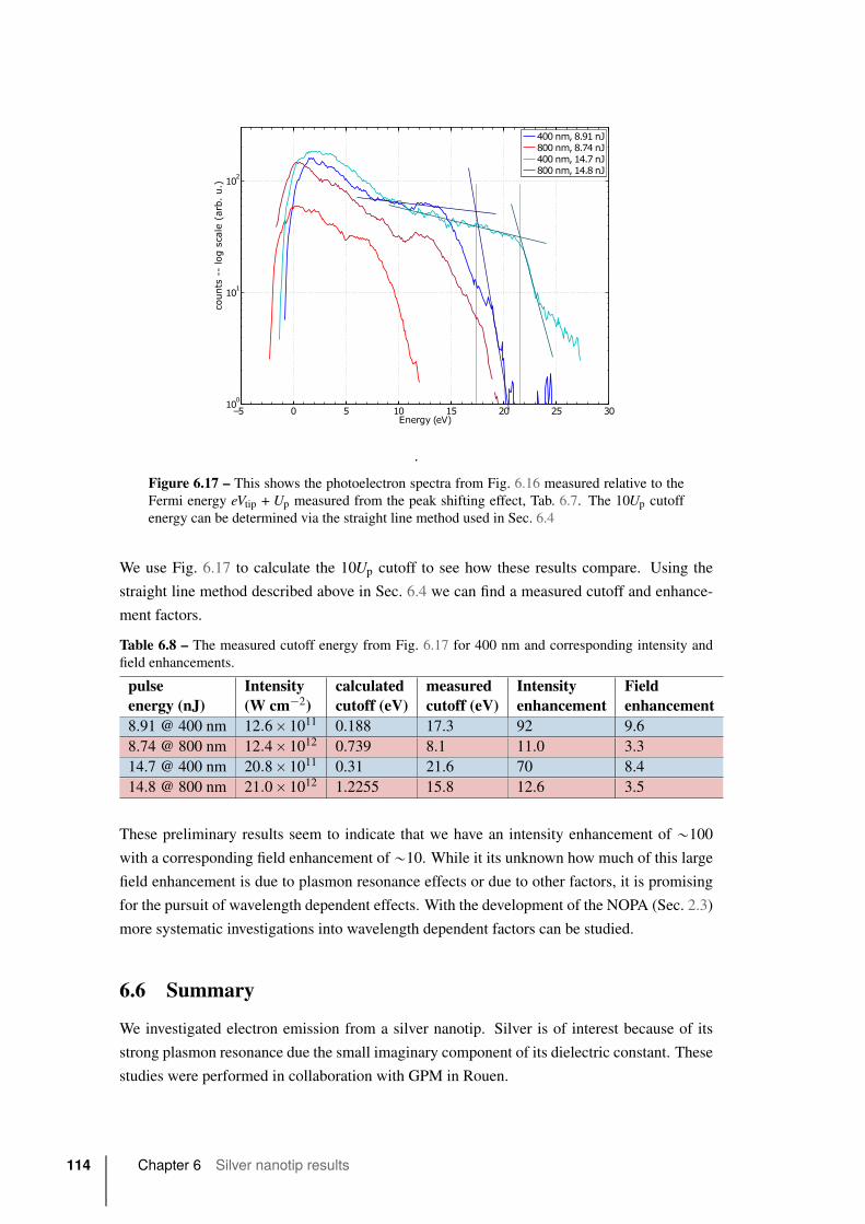
�� � � �� �� �� �� �����
���
���
��������
�����������������������
������������������������������������������������
.
Figure 6.17 – This shows the photoelectron spectra from Fig. 6.16 measured relative to the
Fermi energy eVtip + Up measured from the peak shifting effect, Tab. 6.7. The 10Up cutoff
energy can be determined via the straight line method used in Sec. 6.4
We use Fig. 6.17 to calculate the 10Up cutoff to see how these results compare. Using the
straight line method described above in Sec. 6.4 we can find a measured cutoff and enhance-
ment factors.
Table 6.8 – The measured cutoff energy from Fig. 6.17 for 400 nm and corresponding intensity and
field enhancements.
pulse Intensity calculated measured Intensity Fieldenergy (nJ) (W cm´2) cutoff (eV) cutoff (eV) enhancement enhancement8.91 @ 400 nm 12.6ˆ1011 0.188 17.3 92 9.6
8.74 @ 800 nm 12.4ˆ1012 0.739 8.1 11.0 3.3
14.7 @ 400 nm 20.8ˆ1011 0.31 21.6 70 8.4
14.8 @ 800 nm 21.0ˆ1012 1.2255 15.8 12.6 3.5
These preliminary results seem to indicate that we have an intensity enhancement of „100
with a corresponding field enhancement of „10. While it its unknown how much of this large
field enhancement is due to plasmon resonance effects or due to other factors, it is promising
for the pursuit of wavelength dependent effects. With the development of the NOPA (Sec. 2.3)
more systematic investigations into wavelength dependent factors can be studied.
6.6 Summary
We investigated electron emission from a silver nanotip. Silver is of interest because of its
strong plasmon resonance due the small imaginary component of its dielectric constant. These
studies were performed in collaboration with GPM in Rouen.
114 Chapter 6 Silver nanotip results
We use FIB milled silver tips with known radii of 20-50 nm. The radius was used to corrobo-
rate the Nordheim function used in FN plots. We also used FEM images to observe the multi
emission sites from the polycrystalline nature of the tips.
We irradiated the tip at a high repetition rate. Our first attempts had unexpected results which
we could not account for. We imaged the tip after laser irradiation but found no evidence of
thermal damage nor oxidation. Our second sample yielded results more consistent with our
assumptions. This tip gave a good polarization contrast and fit with n “ 3˘ 0.6, however
spectra yielded high emission to the point of detector saturation so no laser power dependent
exponent could be extracted. We attributed the high emission to possible thermal effects and
lowered the repetition rate of the laser to see if that alleviated the saturation.
At low repetition rate, our polarization scans gave good contrast; however, both laser power
scans as wells as the polarization fit yielded a low extracted η „ 1.5. Possible reasons for
such a low η could be from photofield and thermally enhanced tunneling effects, or geometric
effects such as an angled tip or space charge effects from high emission. Kinetically resolved
spectra revealed a spectral plateau indicating electron recollision and rescattering. We can use
the spectra to calculate the enhacement factor in two ways. First we can calculate Up using
the shift of the spectra from the channel closing peak shifting effect. We can compare these
results to measuring the 10Up energy cutoff from the spectra. Comparing these measured
values with the calculated Up from the applied intensity we find an intensity enhancement
factor of 14.75˘0.05 and a field enhancement of 3.8 ˘ 0.05.
Preliminary results at 400 nm indicate much higher electron emission and much broader en-
ergy spectrum for similar intensities at 400 nm than 800 nm. Again we use the twoUp measure-
ment techniques to determine the enhancement and find and intensity enhancement of „100
with a corresponding field enhancement of „10. While we cannot make firm conclusions as
to whether or not this high enhancement at 400 nm is due to plasmonic resonance effects, it is
a promising start for further wavelength dependent investigations.
Section 6.6 Summary 115


7Re-examining emission mechanisms using
spectral shape
Up until now we have been looking at spectra for an individual tip material and emission
mechanism. In this chapter I compare the emitted spectra and mechanisms presented and
discussed in the previous chapters. I first discuss the probability of photon absorption for an
electron with an above threshold amount of energy. I then describe the expected shapes for
each of the mechanisms and present a schematic of the spectra. I compare the photoelectron
spectra from the previous chapters with the same applied intensities and compare the dominant
emission mechanisms for the various spectra and discuss difficulties in simulating these tip-
based systems.
7.1 ATP peaks: probability of free-free transitions
Recall above threshold photoemission (ATP) where the emitted spectra show characteristic
peaks separated by the applied photon energy corresponding to the number of photons ab-
sorbed by an electron at a given energy. The above threshold absorption of photons is called
the free-free transition [Agostini79]. From the ratio of the number of electrons emitted for a
given peaks of ATP emission, we can determine the “probability” for an electron to absorb a
photon before emission, after it has above threshold energy. An electron has a probability Pn
of being emitted from the system after the absorption of n photons. This means that for an
ATP peak of photon order n an electron has a probability of emission for that energy
Pn “PAT ˆpP1qn´nmin , (7.1)
for n ą nmin, where PAT is the probability of an electron to acquire above threshold energy.
P1 is the probability for an electron to absorb 1 more photon. We find that
P1 “ Jn`1
Jn, (7.2)
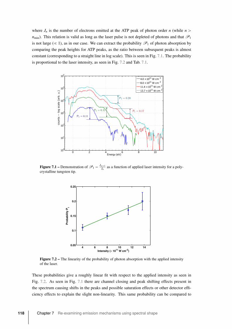
where Jn is the number of electrons emitted at the ATP peak of photon order n (while n ąnmin). This relation is valid as long as the laser pulse is not depleted of photons and that P1
is not large (! 1), as in our case. We can extract the probability P1 of photon absorption by
comparing the peak heights for ATP peaks, as the ratio between subsequent peaks is almost
constant (corresponding to a straight line in log scale). This is seen in Fig. 7.1. The probability
is proportional to the laser intensity, as seen in Fig. 7.2 and Tab. 7.1.
� � � ! �����
���
���
���
���
���
��
� !"#$�%!��
�� ��������#����!�%�"������
������������ �
��������� �
�������� �
�� ������ �
Figure 7.1 – Demonstration of P1 “ Jn`1
Jnas a function of applied laser intensity for a poly-
crystalline tungsten tip.
4 6 8 10 12 140.05
0.1
0.15
0.2
0.25
Intensity (× 1011 W cm−2)
Pro
bab
ility
P1
Figure 7.2 – The linearity of the probability of photon absorption with the applied intensity
of the laser.
These probabilities give a roughly linear fit with respect to the applied intensity as seen in
Fig. 7.2. As seen in Fig. 7.1 there are channel closing and peak shifting effects present in
the spectrum causing shifts in the peaks and possible saturation effects or other detector effi-
ciency effects to explain the slight non-linearity. This same probability can be compared to
118 Chapter 7 Re-examining emission mechanisms using spectral shape

Table 7.1 – A list of P1 probabilities extracted from Fig. 7.1 as a function of applied laser intensity.
Intensity (W cm´2) P111
4.0 ˆ1011 W cm´2 0.11
8.0 ˆ1011 W cm´2 0.15
11.4 ˆ1011 W cm´2 0.17
13.7 ˆ1011 W cm´2 0.20
other examples of ATP peaks as well as above threshold ionization (ATI) peaks in atoms. For
example, ionization in Xe atoms from [Agostini79] yields a free-free transition probability,
P1, of „0.15 for a laser intensity of 8ˆ1012 W cm´2. This is a much higher intensity than
for equivalent probabilities we found for tungsten nanotips. This is possibly due to the higher
ionization potential of a Xe atom compared to the work function of a tungsten nanotip, or due
to the lack of field enhancement in atoms. For the tungsten tips found in [Schenk10], a P1 of
„0.3 was found for a laser intensity of 2.3ˆ1011 W cm´2. This is a much higher probability
than we found for similar laser intensities. However, the tungsten tips used in [Schenk10] were
a factor of two smaller than ours indicating a higher field enhancement and their laser pulses
were much shorter possibly alleviating thermal effects which might have slightly surpressed
the magnitude of our peaks.
7.2 Spectral shape
7.2.1 Different shapes for different mechanisms
We use the shape of the spectra to identify emission mechanisms. Fig. 7.3 shows a schematic
of the different spectral shapes we identified.
Electron kinetic energy (eV)
Ele
ctro
n yi
eld
(log
scal
e)
Figure 7.3 – This shows a schematic of the spectral shapes identified in this thesis. The
blue portion represents thermally enhanced field emission (Sec. 1.2.3), the green represents
above threshold photoemission (ATP, Sec. 1.3.2) and the red is from rescattering electrons
(Sec. 1.3.3). The spectra we expect for each mechanism are represented by the solid lines.
Section 7.2 Spectral shape 119
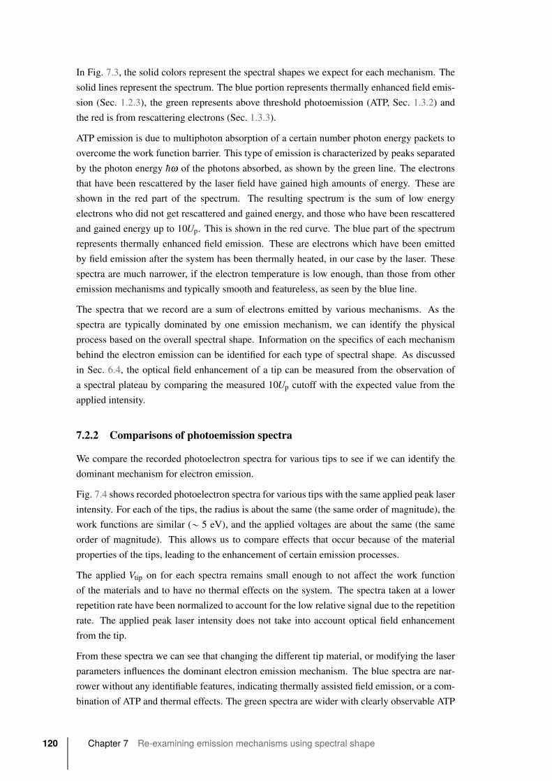
In Fig. 7.3, the solid colors represent the spectral shapes we expect for each mechanism. The
solid lines represent the spectrum. The blue portion represents thermally enhanced field emis-
sion (Sec. 1.2.3), the green represents above threshold photoemission (ATP, Sec. 1.3.2) and
the red is from rescattering electrons (Sec. 1.3.3).
ATP emission is due to multiphoton absorption of a certain number photon energy packets to
overcome the work function barrier. This type of emission is characterized by peaks separated
by the photon energy hω of the photons absorbed, as shown by the green line. The electrons
that have been rescattered by the laser field have gained high amounts of energy. These are
shown in the red part of the spectrum. The resulting spectrum is the sum of low energy
electrons who did not get rescattered and gained energy, and those who have been rescattered
and gained energy up to 10Up. This is shown in the red curve. The blue part of the spectrum
represents thermally enhanced field emission. These are electrons which have been emitted
by field emission after the system has been thermally heated, in our case by the laser. These
spectra are much narrower, if the electron temperature is low enough, than those from other
emission mechanisms and typically smooth and featureless, as seen by the blue line.
The spectra that we record are a sum of electrons emitted by various mechanisms. As the
spectra are typically dominated by one emission mechanism, we can identify the physical
process based on the overall spectral shape. Information on the specifics of each mechanism
behind the electron emission can be identified for each type of spectral shape. As discussed
in Sec. 6.4, the optical field enhancement of a tip can be measured from the observation of
a spectral plateau by comparing the measured 10Up cutoff with the expected value from the
applied intensity.
7.2.2 Comparisons of photoemission spectra
We compare the recorded photoelectron spectra for various tips to see if we can identify the
dominant mechanism for electron emission.
Fig. 7.4 shows recorded photoelectron spectra for various tips with the same applied peak laser
intensity. For each of the tips, the radius is about the same (the same order of magnitude), the
work functions are similar („ 5 eV), and the applied voltages are about the same (the same
order of magnitude). This allows us to compare effects that occur because of the material
properties of the tips, leading to the enhancement of certain emission processes.
The applied Vtip on for each spectra remains small enough to not affect the work function
of the materials and to have no thermal effects on the system. The spectra taken at a lower
repetition rate have been normalized to account for the low relative signal due to the repetition
rate. The applied peak laser intensity does not take into account optical field enhancement
from the tip.
From these spectra we can see that changing the different tip material, or modifying the laser
parameters influences the dominant electron emission mechanism. The blue spectra are nar-
rower without any identifiable features, indicating thermally assisted field emission, or a com-
bination of ATP and thermal effects. The green spectra are wider with clearly observable ATP
120 Chapter 7 Re-examining emission mechanisms using spectral shape

−2 0 2 4 6 8 10 12 140
1
2
3
4
5
6
Energy (eV)
Co
un
ts (
log
sca
le, n
orm
aliz
ed)
Peak laser intensity ∼6E11W cm−2
CC4 15 V, 20 mW, MHzSCW 15 V, 20 mW, MHzAg 50 V, 8.74 nJ, kHz
0 5 10 15 200
1
2
3
4
5
6
Energy (eV)
Co
un
ts (
log
sca
le, n
orm
aliz
ed)
Peak laser intensity ∼1E12W cm−2
Ag 20 V, 50 mW, MHzSCW 15 V, 50 mW, MHzAg 50 V, 14.8 nJ, kHz
Figure 7.4 – Each set of spectrum were taken with the same applied peak laser intensity:
top 6 ˆ 1011 W cm´2, bottom 1 ˆ 1012 W cm´2. Changing the tip material or laser
repetition rate (mean power) changes the dominant emission mechanism. The blue spectra
show narrower spectra indicating thermally enhanced field emission. The green spectra show
multiphoton emission characterized by ATP peaks separated by the photon energy. The red
spectra show much broader energies indicating a transition into the optical tunneling regime
and the emergence of a spectral plateau for high intensity evidencing electron recollision and
rescattering.
peaks indicating multiphotonic, over the barrier emission. The red spectra are much wider and
show the emergence of the characteristic spectral plateau from optical tunneling and electron
rescattering and recollision.
For top panel in Fig. 7.4, all spectra were taken with an applied intensity of 6ˆ 1011 W cm´2.
Section 7.2 Spectral shape 121
The blue spectrum is from a CCnT at high repetition rate and has much narrower indicating
thermal assisted field emission is the dominant mechanism. The green spectrum is from a
SCW(310) nanotip at high repetition rate with a slightly broader spectrum than for the CCnT
with visible ATP peaks up to a photon order of n “ 5 (three visible peaks). The red spec-
trum is from a polycrystalline Ag nanotip taken at low repetition rate. The energies of these
photoelectrons form a much broader spectrum possibly indicating a transition into the optical
tunneling regime.
The bottom spectra in Fig. 7.4 were all taken with an applied intensity of 1 ˆ 1012 W cm´2.
The green spectrum is from a SCW(310) nanotip. The wider spectrum and characteristic ATP
peaks separated by the photon energy of the laser indicate multiphotonic emission up to a
photon order of n “ 9. The blue spectrum is from a polycrystalline AG nanotip taken at high
repetition rate. The narrowness and featureless spectrum indicates the electrons were emitted
with thermal assistance from the laser, possibly due to the high mean power. By reducing
the repetition rate of the laser, the mean power of the laser becomes almost negligible. This
alleviates thermal effects from the laser and the spectrum becomes much broader and a plateau
forms indicating electron recollision and rescattering.
The indicated applied intensities do not take into account the field enhancement from the
nanotips. The enhancement takes into account both the tip geometry and material. As seen
by the various spectral shapes expressing the different emission mechanisms, the different
enhancement factors of the tips augment the dominant emission mechanisms. Lowering the
repetition rate of the laser alleviates the thermal effects of high mean power allowing other
emission mechanism to dominate.
From this we see that the repetition rate of the laser has the largest effect on the dominant
emission mechanism as it negates thermal effects from high mean power. For the same silver
tip, we are able to observe thermal emission for high mean power laser and repetition rate
irradiation, and electron recollision and rescattering for low mean powers. The intensity of
the laser allows these spectral features to become more pronounced. The tip material also
factors in as tungsten is the only material for which ATP emission was observable for high
repetition rates, while the size of the tip affects the optical enhancement factors from the laser
without adding thermal effects that come with higher mean power or intensity. Future investi-
gations using the NOPA (Sec. 2.3) will allow further studies in wavelength and repetition rate
dependencies.
7.2.3 Spectral simulations
Theoretical modeling of thermally assisted field emission is not as straight forward as there
are many factors that must be taken into account [Kealhofer12]. All the contributions to the
thermal balance of the system are not evident, and include parameters such as the thermal
conductivity of the material, the transfer of heat energy to the electrons and from the electrons
to the lattice ions, emission of electrons, the application of the tip bias, etc. Finite element
modeling of the evolution of temperature within the tip has been done to assess the thermal
122 Chapter 7 Re-examining emission mechanisms using spectral shape
thresholds of tips [Houard11, Kealhofer12]. From these studies we can make first order ap-
proximations on the emitted spectra of thermally assisted field emission. We know that these
spectra are generally narrower than those emitted by multiphonic absorption and the slope
(and width) of the emitted spectra depends on the electron temperature and the static electric
field from the tip bias.
Simulations on atomic and molecular systems on above threshold ionization (ATI) and rescat-
tering electron emission effects have been extensively studied [Corkum93, Paulus94a, Ivanov05].
Expansion of these calculations to tip based systems is also under investigation [Krüger12b,
Ciappina14a, Ciappina14b], but application of field enhancement effects is not evident as the
field is not homogeneous. Tip based systems must also take into account other parameters
which are not considered (or relevant) for atomic systems such as: the geometric shape of the
system, the bulk energy band structure of the electron states (as opposed to discrete energy
levels), the thermal effects of the system, the surface interface of the system with the vacuum
and corresponding surface interaction effects, as well as the low work function for a metal
(„5 eV) compared to the ionization potential of an atom („15 eV).
7.3 Summary
In this chapter I present a comparison of the spectrum seen in this thesis. I first discuss the
probability of free-free transitions where an above threshold electron can absorb another pho-
ton. This probability can be derived from the heights of the ATP peaks. I then discuss the
expected spectral shapes for thermally assisted field emission, above threshold photoemission
and electron recollision and rescattering. I present a schematic of each of the expected electron
spectrum. I then compare spectra from different tips for the same applied laser intensity. We
see the narrower spectra and lack of ATP peaks from thermally enhanced electron emission
for a CCnT and Ag nanotip at high repetition rate. Multiphotonic photoemission is seen for
SCW(310) with peaks in the spectrum indicate one more photon absorbed by the system and
are separated by the photon energy. Finally we see signs of electron recollision and scattering
in the photoemission spectrum for Ag. The laser repetition rate has been reduced, so that the
mean power is almost negligible. The spectrum is much broader than emission from other
mechanisms. A plateau forms at higher intensities indicating electron recollision. Finally I
present some of the difficulties in simulating spectra from tips, as tip-based systems are not as
straight forward as those on atoms and molecules.
Section 7.3 Summary 123

Conclusion and Perspectives
In this thesis I present a novel experiment for investigating photoelectron emission induced by
an ultrafast laser from a sharp nanotip. This new scientific direction for my group involved the
complete design and development of a new experimental setup and apparatus incorporating
existing electron spectroscopy techniques with laser development expertise. We expand upon
previous results in conventional metallic nanotips of tungsten [Hommelhoff06b, Barwick07,
Yanagisawa10] and gold [Ropers07, Bormann10, Park12] by using innovative new tips based
on carbon nanotubes and silver.
The physical mechanisms behind electron emission induced by light have been studied since
the discovery of the photoelectric effect by Einstein in 1905. Chapter 1 presents an overview
of the physical processes for electron emission from a metal surface, and the peculiarities
that arise from a sharp nanotip geometry. There are three main mechanisms behind electron
emission from a system, depending on the field applied and the laser intensity illuminating the
system. By changing the parameters applied to our system (applied voltage, nanotip material
and radius, laser intensity, photon energy and repetition rate), we can change and control the
dominant emission process observed. With no laser, the system can be heated up such that
the electrons can obtain sufficient energy to overcome the work function of the material, or
a strong enough external DC field can be applied so that the barrier becomes penetrable via
quantum mechanical tunneling. With the addition of a low to moderate laser pulse, and an
external electric field, an electron can be emitted via assisted tunneling by either the absorption
of a photon or from the tail of the laser heated electron gas within the metal. With moderate
to high laser intensities, the system can absorb enough energy from the laser to overcome the
potential barrier of the system, and at high enough intensities, the optical field of the laser acts
and modify the barrier itself to induce tunneling and possibly rescattering and recollision of
the electron with the system.
All these mechanisms of electron emission are valid not just for nanotip systems. The sharp
nanotip geometry adds factors to the system that must be taken into account. A simple geomet-
ric field enhancement is seen at the apex of the tip simply due to the nanometer sized tip, where
the field at the end of the apex is given by F “ βVtip. A corresponding optical field enhance-
ment is also considered when assessing nanotip geometries. This can lead to modifications in
the electron propagation, steering the electrons away from their normal trajectories.
Chapters 2 and 3 describe in detail the experimental apparatus and methods for our investi-
gations. We implement a fully characterized and controllable laser system based on a con-
ventional 800 nm, Ti:sapphire laser oscillator and amplifier chain. This system can be used
in a high repetition rate (62 MHz), moderate mean power mode, using the direct output from
the oscillator, or a low repetition rate (1 kHz), low mean power mode using the regenerative
amplifier, each mode with the same peak pulse intensity. We have also built a NOPA at the
output of a fiber-based infrared laser which allows flexibility in wavelength and repetition rate,
while maintaining short pulse duration and the same peak pulse intensity. This NOPA system
has yet to be implemented in the experimental setup. Our new experimental apparatus is fully
flexible to allow for the variety of parameters we can change. We have access to three types
of nanotips, tungsten, silver and carbon nanotube based tips, each of which requires a slightly
different mounting technique within our ultrahigh vacuum chamber. We use three dimensional
nanopositioning stages to position the tips into the focus of the laser. The emitted electrons
are detected in a homemade field retarding spectrometer, from which we record an integrated
electron spectra. Later generations of the spectrometer can move in two dimensions allowing
for spatially resolved, FEM-like measurements.
We compare our experimental setup to existing experiments using our results on tungsten
nanotips in Chapter 4. We are able to confirm that our in-situ tip characterization techniques
correspond with our assumptions on the size of the tip apex as well as the predicted emission
sites. Using polarization dependence curves and the laser power dependence, we are able to
extract the average number of photons, η „ 3, the system absorbs before electron emission.
This corresponds well with the minimum number of photons needed nmin “ φ{hω “ 2.9 to
overcome the work function barrier φ “ 4.35 eV of single crystal (310) tungsten. Kinetically
resolved photoelectron spectra show easily observable ATP peaks. Power dependency for
each peak confirm that each peak corresponds to a different number of absorbed photons. Our
results on tungsten allow us to validate our experimental setup as well as familiarize us with
this new setup.
Chapters 5 and 6 present results on novel nanotips. Studies on emission from CCnTs (Chap-
ter 5) are performed in collaboration with CEMES in Toulouse. CCnTs provide an interesting
sample from which to study electron emission. These samples are based on a single carbon
nanotube surrounded by concentric graphene sheets to form a conical shape. As the formation
and synthesis of these tips was fully developed in house, control parameters can be imple-
mented to exhibit certain specifications in the CCnTs that are valued for our experiments.
Electron emission polarization dependency result yields an average number of photons ab-
sorbed before emission of 3.4, consistent with the minimum number of photons needed to
overcome the φ “ 5.0 eV work function of a CCnT. However, moderate laser intensity lead to
the modification and destruction of samples due to laser irradiation. Systematic studies on the
damage threshold of CCnTs due to laser illumination lead to a maximum applicable peak in-
tensity of around„7.7ˆ 1011 W cm´2 at high repetition rate. Using intensities less than this,
we are able to record photoelectron spectra. These spectra show no signs of ATP phenomenon
and the narrowness of their energy bandwidth compared to those of similar intensities taken
from tungsten seems to indicate emission due to thermal effects on the system.
126 Conclusion and Perspectives

Investigations on silver nanotips (Chapter 6) are done in collaboration with GPM in Rouen.
Silver is of interest due to its strong plasmonic response because of the small imaginary com-
ponent of its dielectric component. This corresponds to a resonance near 400 nm, which is
easily reachable with our laser system. At high repetition rate (moderate mean power), we
extract an average of 3 absorbed photons of the system before emission of an electron, con-
sistent with the φ “ 4.26 eV work function of polycrystalline silver. However, kinetically
resolved spectra yield high emission, saturating the detectors, so no laser power dependent
exponent can be extracted. These spectra are also very narrow in energy, indicating possible
thermal effect aiding with the emission process. Low repetition rate yields a low extracted
number of photons absorbed by the system. Possible reasons for such a low number could be
from emission caused by tunneling effects or geometric factors such as space charge effects
or angled nanotips. Kinetically resolved spectra demonstrate the first observance of a spectral
plateau indicating electron recollision and rescattering. From the spectral features we can cal-
culate an intensity enhancement of 14.75˘0.05 with corresponding field enhancement of 3.8
˘ 0.05. Preliminary results from 400 nm irradiation indicate higher electron yield and broader
spectrum for similar intensities at 400 nm than 800 nm.
We compare the spectra presented in Chapters 4, 5 and 6 in Chapter 7. Here we show that we
are able to identify different dominant photoelectron emission mechanisms based on spectral
shape. We compare spectra from various tips with the same applied laser intensities, not taking
into account enhancement form the tips. Using the appearance of multiphotonic ATP peaks
in tungsten emission as a baseline, we are able to see narrower spectra from high repetition
rate result from CCnTs and silver nanotips indicating thermally assisted electron emission.
Silver electron emission for low repetition gives broader electron spectra and the appearance
of a spectral plateau, indicating the possibly the thermal effects from high repetition rate are
suppressing the recollision effects of the laser field.
This thesis by no means presents an exhaustive study on the subject of electron emission from
sharp nanotips, or even from these three materials. As we have been limited by thermal effects
in our emission mechanisms, more investigation into these effects would be useful for future
experiments. It would be interesting to see at what point emission from say, a silver nanotip
switches from predominantly thermal emission to laser-induced and strong field effects. This
would also give a time scale as to how long such elevated thermal states last. Such a study
could be performed by investigating the emitted spectral shape as a function of repetition rate
of the laser. The mechanisms of thermal emission are also not fully understood and thorough
simulations are needed to corroborate our experimental results.
Investigations into the plasmonic response of materials would provide great insight into wave-
length dependent emission mechanisms. Already preliminary results indicate there is higher
electron yield and broader spectrum for laser irradiation close to the predicted plasmon reso-
nance. Systematic studies on the electron yield as a function of wavelength close to the pre-
dicted resonance or even spectral shape could provide some insight to how these resonances
affect the electron properties of these nanotips.
The flexibility of our experimental setup allows us the possibility to collect the laser light af-
127

ter it has interacted with the tip. As optical tunneling, electron rescattering and recollision
are the same physical mechanisms behind high harmonic generation, perhaps slight modifi-
cations to our system would allow us to observe harmonics caused by the tips. Pump-probe
experiments could provide insight to properties of the electron bunches themselves, and from
pump-probe spectroscopy experiments we could extract optical properties of our nanostruc-
tures. The emission from tips can be used to study fundamental properties on electrons such
as electron interference [Barwick08, Vidil] and for matter wave experiments.
The experiment presented in this thesis allows us flexibility to explore light-matter interactions
in a unique regime between atomic and condensed states created by a sharp nanotips. We probe
investigations into the electron emission from such a system and the parameters that influence
the dominant physical mechanisms of emission. The combination of laser expertise and novel
materials allows a push to strong field phenomenon and applications for these systems.
128 Conclusion and Perspectives

AList of Symbols and Abbreviations
β field amplification factor, 1{kr
δ adiabaticity parameter for elec-
tron propagation
η extracted power exponent
γ Keldysh parameter
h reduced Planck constant
λ laser wavelength
E electric field of a laser pulse
e Euler’s number
μ Fermi energy
ω photon angular frequency
φ work function
Φptq temporal phase of a laser pulse
k wave vector
ϕpωq spectral phase of a laser pulse
c vacuum speed of light
e electric charge
F applied field
I laser intensity
J current density of emission
k dimensionless factor depending
on shape of tip and the extrac-
tion geometry
kB Boltzman constant
me electron mass
n number of photons absorbed by
the system
r radius of the nanotip
T temperature
Upxq potential barrier seen by an
electron at position x
ε0 permittivity of free space
Up ponderomotive energy
Vretard retarding field of spectrometer
Vtip nanotip bias
ATI Above Threshold Ionization
ATP Above Threshold Photo-
emission
BBO β -barium borate crystal
CCD charge-coupled device
CCnT Carbon Cone nanoTip
CEMES Centre d’Élaboration deMatéri-
aux et d’Etudes Structurales,
Toulouse, France
CEP carrier envelope phase
cw continuous wave
DC direct current
DFG difference frequency generation
FEM field emission microscopy
FIB Focused Ion Beam
FN Fowler-Nordheim
fwhm full width at half maximum
GDD group delay dispersion
GPM Groupe de Physique desMatéri-
aux, Rouen, France
GVM group velocity mismatch
HHG high harmonic generation
IR infrared
KLM Kerr lens modelock
LOPT lowest order perturbation the-
ory
LX SPIDER Long Crystal Spectral Phase
Interferometry for Direct
Electrid-field Reconstruction
MCP microchannel plate
NEG non-evaporable getter
NOPA non-collinear optical paramet-
ric amplifier
OAP off-axis parabola
OPA optical parametric amplification
PCW polycrystalline tungsten
regen regenerative amplifier
RGA residual gas analyzer
SCW single crystal tungsten
SEM Scanning Electron Microscope
SF super fluorescence
SHG second harmonic generation
TFP thin film polarizer
Ti:sapphire titanium doped sapphire
TOD third order dispersion
TSM Three Step Model
TTL transistor-transistor logic
UHV ultra-high vacuum
WLC white light continuum
YAG yttrium aluminum garnet,
Y3Al5O12
130 Appendix A List of Symbols and Abbreviations
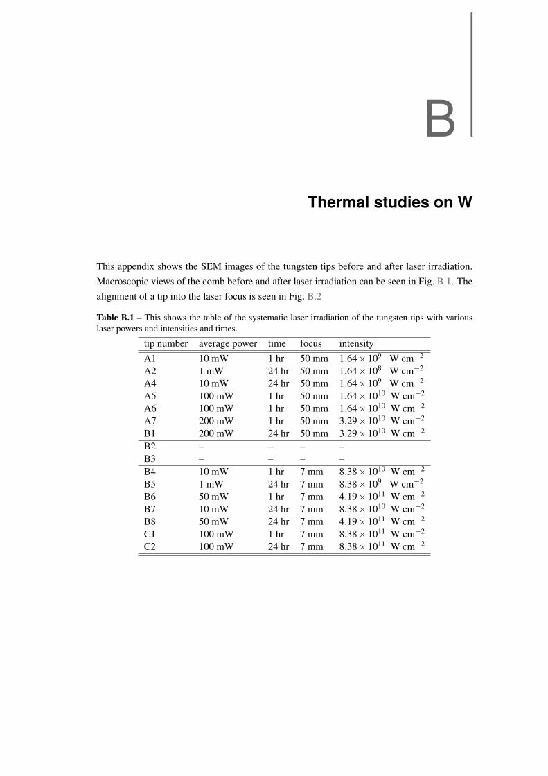
BThermal studies on W
This appendix shows the SEM images of the tungsten tips before and after laser irradiation.
Macroscopic views of the comb before and after laser irradiation can be seen in Fig. B.1. The
alignment of a tip into the laser focus is seen in Fig. B.2
Table B.1 – This shows the table of the systematic laser irradiation of the tungsten tips with various
laser powers and intensities and times.
tip number average power time focus intensity
A1 10 mW 1 hr 50 mm 1.64ˆ109 W cm´2
A2 1 mW 24 hr 50 mm 1.64ˆ108 W cm´2
A4 10 mW 24 hr 50 mm 1.64ˆ109 W cm´2
A5 100 mW 1 hr 50 mm 1.64ˆ1010 W cm´2
A6 100 mW 1 hr 50 mm 1.64ˆ1010 W cm´2
A7 200 mW 1 hr 50 mm 3.29ˆ1010 W cm´2
B1 200 mW 24 hr 50 mm 3.29ˆ1010 W cm´2
B2 – – – –
B3 – – – –
B4 10 mW 1 hr 7 mm 8.38ˆ1010 W cm´2
B5 1 mW 24 hr 7 mm 8.38ˆ109 W cm´2
B6 50 mW 1 hr 7 mm 4.19ˆ1011 W cm´2
B7 10 mW 24 hr 7 mm 8.38ˆ1010 W cm´2
B8 50 mW 24 hr 7 mm 4.19ˆ1011 W cm´2
C1 100 mW 1 hr 7 mm 8.38ˆ1011 W cm´2
C2 100 mW 24 hr 7 mm 8.38ˆ1011 W cm´2

Figure B.1 – Left: Macroscopic view of the comb before the thermal tests. Right: Macro-
scopic view of the comb after the thermal tests, note the two end tips have fallen off.
Figure B.2 – This shows the alignment of tip A4 in the focus of the laser with 250 μW of
average power.
132 Appendix B Thermal studies on W
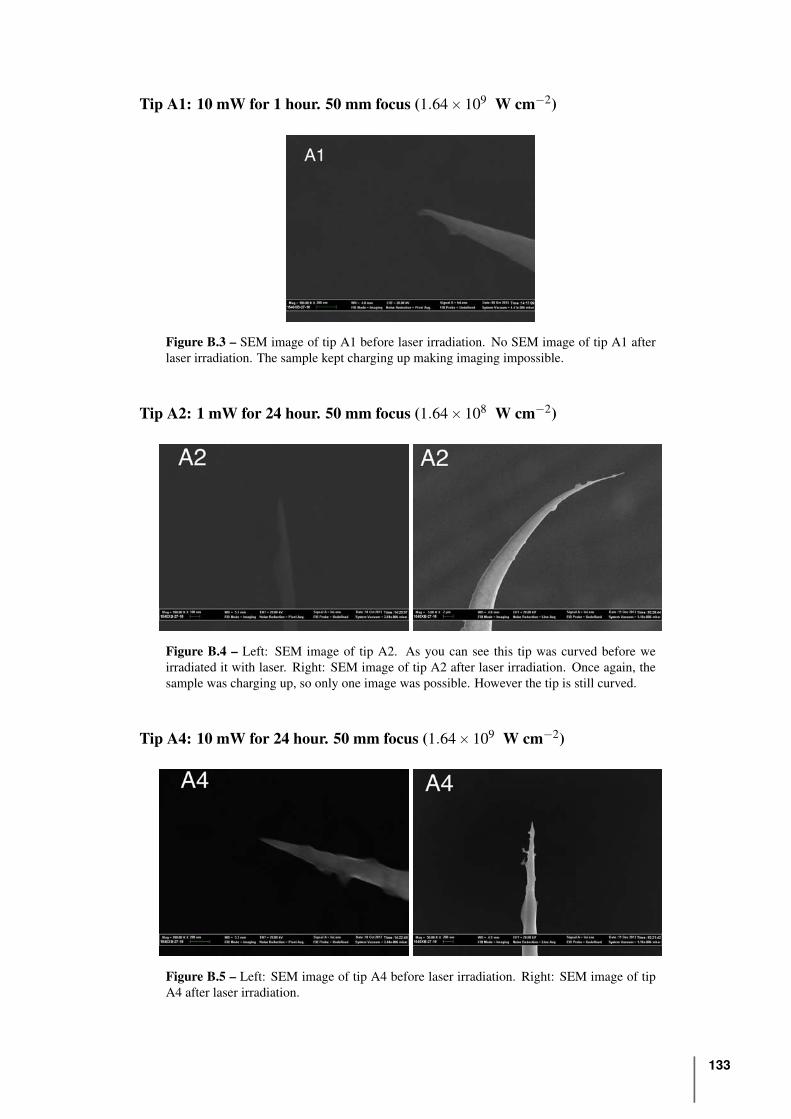
Tip A1: 10 mW for 1 hour. 50 mm focus (1.64ˆ109 W cm´2)
Figure B.3 – SEM image of tip A1 before laser irradiation. No SEM image of tip A1 after
laser irradiation. The sample kept charging up making imaging impossible.
Tip A2: 1 mW for 24 hour. 50 mm focus (1.64ˆ108 W cm´2)
Figure B.4 – Left: SEM image of tip A2. As you can see this tip was curved before we
irradiated it with laser. Right: SEM image of tip A2 after laser irradiation. Once again, the
sample was charging up, so only one image was possible. However the tip is still curved.
Tip A4: 10 mW for 24 hour. 50 mm focus (1.64ˆ109 W cm´2)
Figure B.5 – Left: SEM image of tip A4 before laser irradiation. Right: SEM image of tip
A4 after laser irradiation.
133
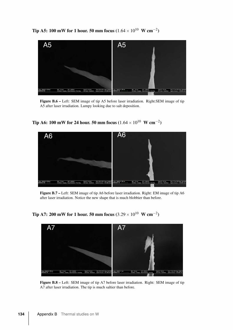
Tip A5: 100 mW for 1 hour. 50 mm focus (1.64ˆ1010 W cm´2)
Figure B.6 – Left: SEM image of tip A5 before laser irradiation. Right:SEM image of tip
A5 after laser irradiation. Lumpy looking due to salt deposition.
Tip A6: 100 mW for 24 hour. 50 mm focus (1.64ˆ1010 W cm´2)
Figure B.7 – Left: SEM image of tip A6 before laser irradiation. Right: EM image of tip A6
after laser irradiation. Notice the new shape that is much blobbier than before.
Tip A7: 200 mW for 1 hour. 50 mm focus (3.29ˆ1010 W cm´2)
Figure B.8 – Left: SEM image of tip A7 before laser irradiation. Right: SEM image of tip
A7 after laser irradiation. The tip is much saltier than before.
134 Appendix B Thermal studies on W
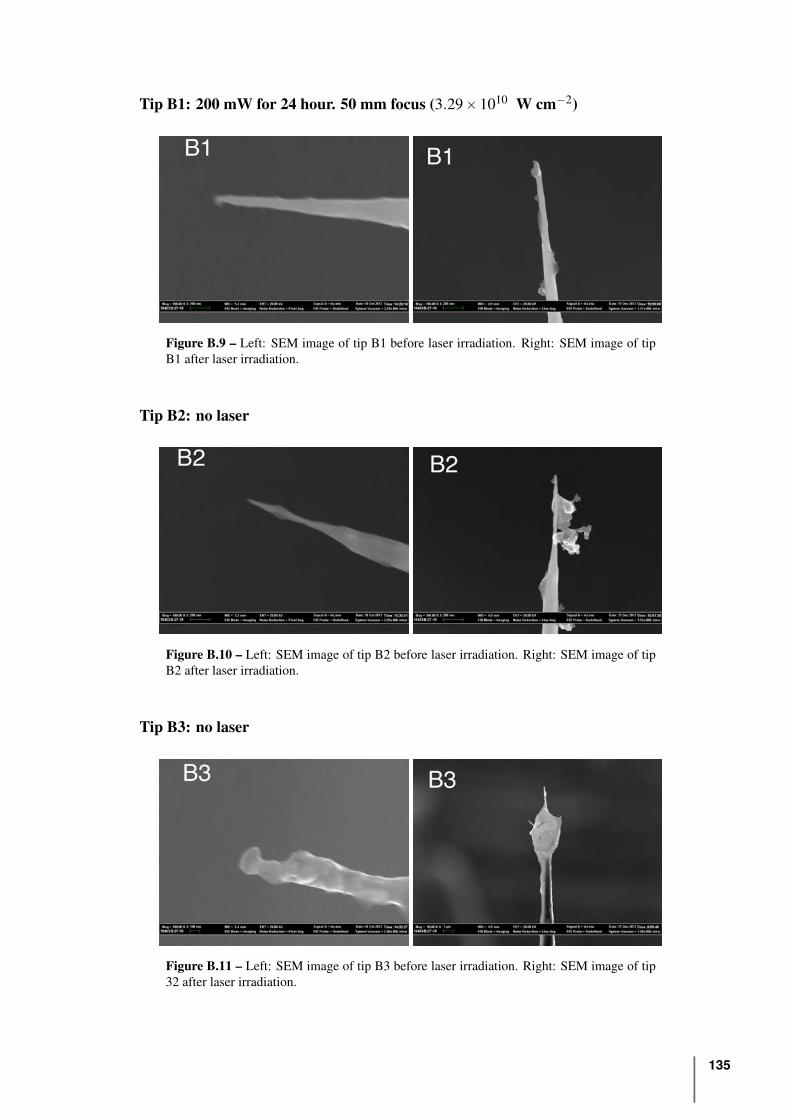
Tip B1: 200 mW for 24 hour. 50 mm focus (3.29ˆ1010 W cm´2)
Figure B.9 – Left: SEM image of tip B1 before laser irradiation. Right: SEM image of tip
B1 after laser irradiation.
Tip B2: no laser
Figure B.10 – Left: SEM image of tip B2 before laser irradiation. Right: SEM image of tip
B2 after laser irradiation.
Tip B3: no laser
Figure B.11 – Left: SEM image of tip B3 before laser irradiation. Right: SEM image of tip
32 after laser irradiation.
135
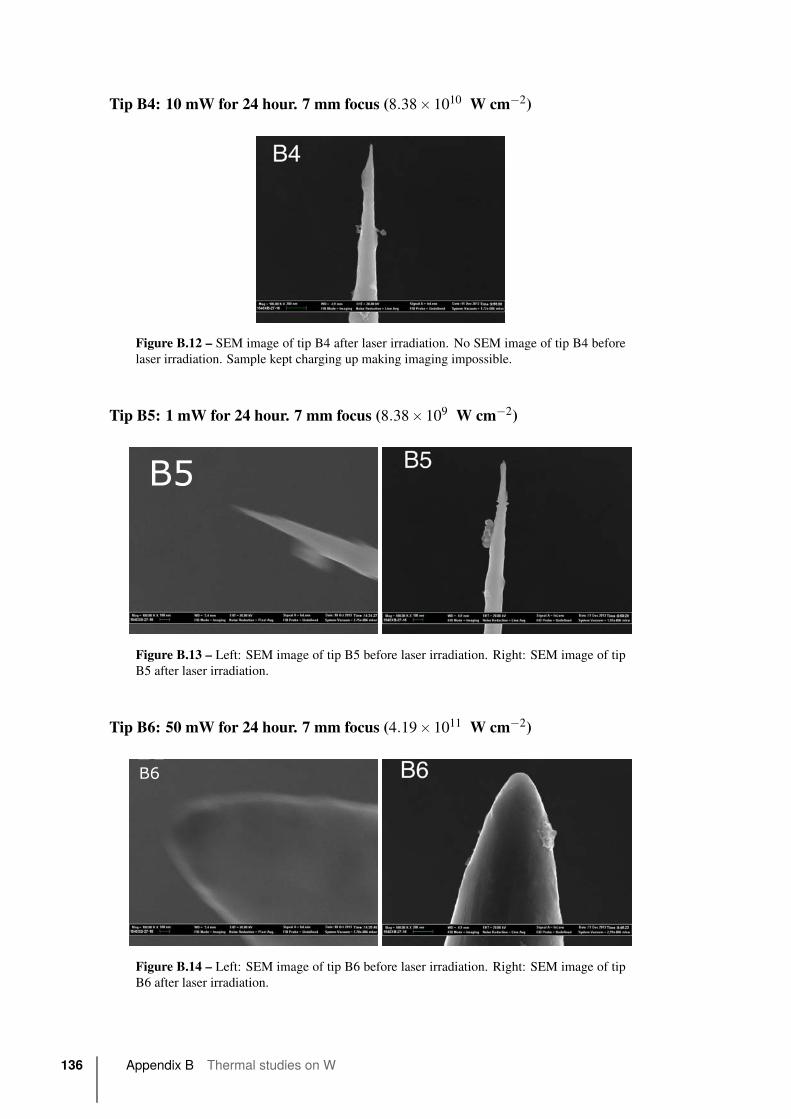
Tip B4: 10 mW for 24 hour. 7 mm focus (8.38ˆ1010 W cm´2)
Figure B.12 – SEM image of tip B4 after laser irradiation. No SEM image of tip B4 before
laser irradiation. Sample kept charging up making imaging impossible.
Tip B5: 1 mW for 24 hour. 7 mm focus (8.38ˆ109 W cm´2)
��
Figure B.13 – Left: SEM image of tip B5 before laser irradiation. Right: SEM image of tip
B5 after laser irradiation.
Tip B6: 50 mW for 24 hour. 7 mm focus (4.19ˆ1011 W cm´2)
��
Figure B.14 – Left: SEM image of tip B6 before laser irradiation. Right: SEM image of tip
B6 after laser irradiation.
136 Appendix B Thermal studies on W
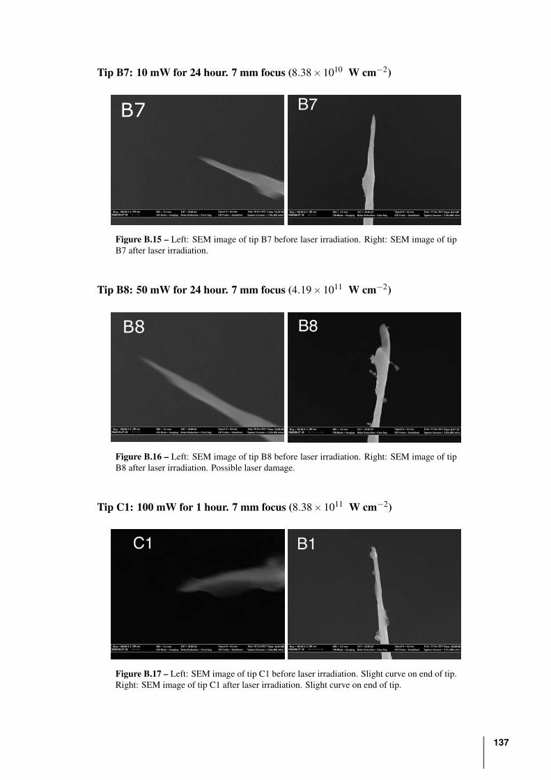
Tip B7: 10 mW for 24 hour. 7 mm focus (8.38ˆ1010 W cm´2)
�&
Figure B.15 – Left: SEM image of tip B7 before laser irradiation. Right: SEM image of tip
B7 after laser irradiation.
Tip B8: 50 mW for 24 hour. 7 mm focus (4.19ˆ1011 W cm´2)
��
Figure B.16 – Left: SEM image of tip B8 before laser irradiation. Right: SEM image of tip
B8 after laser irradiation. Possible laser damage.
Tip C1: 100 mW for 1 hour. 7 mm focus (8.38ˆ1011 W cm´2)
Figure B.17 – Left: SEM image of tip C1 before laser irradiation. Slight curve on end of tip.
Right: SEM image of tip C1 after laser irradiation. Slight curve on end of tip.
137
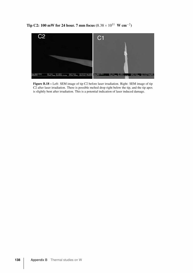
Tip C2: 100 mW for 24 hour. 7 mm focus (8.38ˆ1011 W cm´2)
Figure B.18 – Left: SEM image of tip C2 before laser irradiation. Right: SEM image of tip
C2 after laser irradiation. There is possible melted drop right below the tip, and the tip apex
is slightly bent after irradiation. This is a potential indication of laser induced damage.
138 Appendix B Thermal studies on W
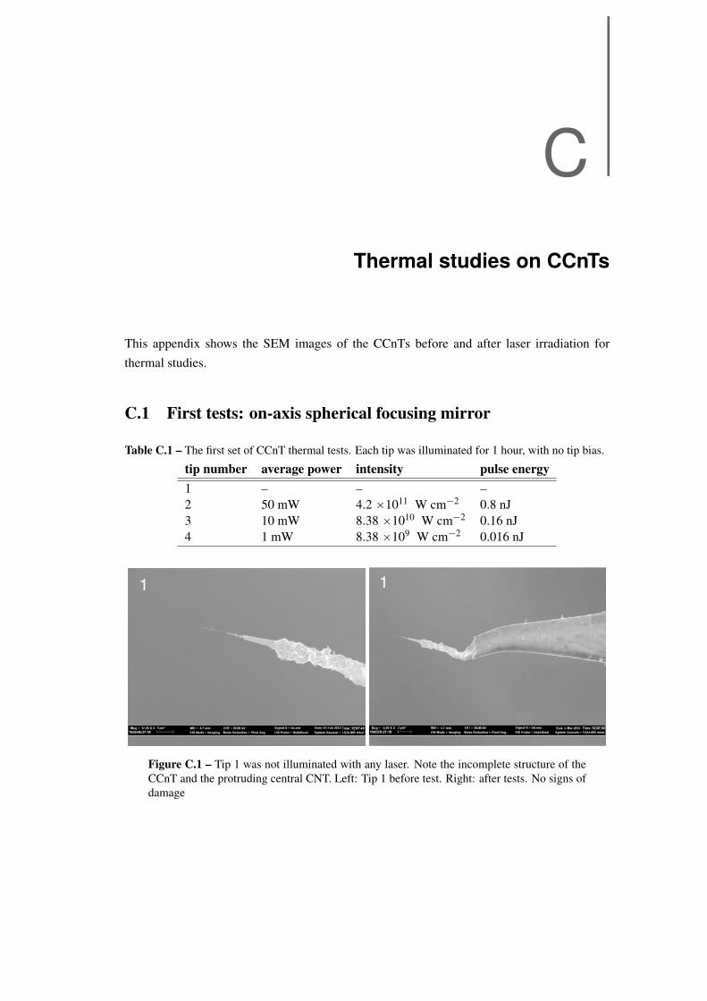
CThermal studies on CCnTs
This appendix shows the SEM images of the CCnTs before and after laser irradiation for
thermal studies.
C.1 First tests: on-axis spherical focusing mirror
Table C.1 – The first set of CCnT thermal tests. Each tip was illuminated for 1 hour, with no tip bias.
tip number average power intensity pulse energy1 – – –
2 50 mW 4.2 ˆ1011 W cm´2 0.8 nJ
3 10 mW 8.38 ˆ1010 W cm´2 0.16 nJ
4 1 mW 8.38 ˆ109 W cm´2 0.016 nJ
Figure C.1 – Tip 1 was not illuminated with any laser. Note the incomplete structure of the
CCnT and the protruding central CNT. Left: Tip 1 before test. Right: after tests. No signs of
damage
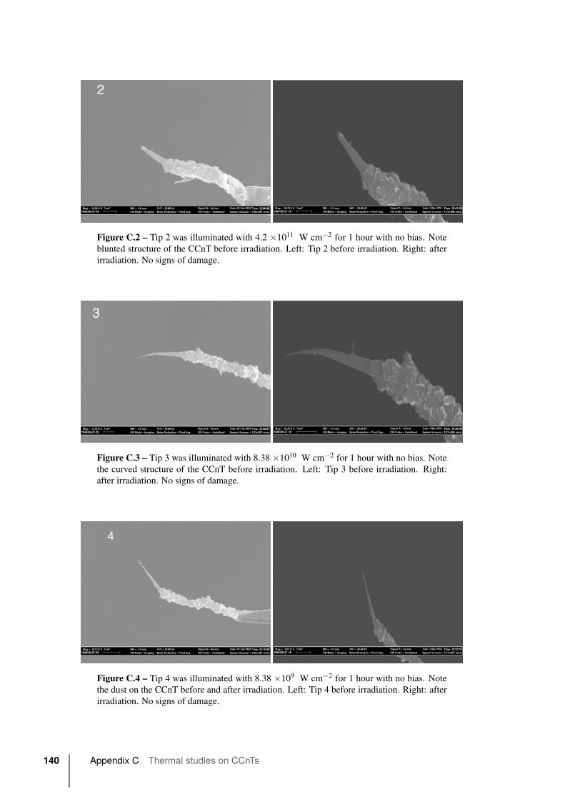
Figure C.2 – Tip 2 was illuminated with 4.2 ˆ1011 W cm´2 for 1 hour with no bias. Note
blunted structure of the CCnT before irradiation. Left: Tip 2 before irradiation. Right: after
irradiation. No signs of damage.
Figure C.3 – Tip 3 was illuminated with 8.38 ˆ1010 W cm´2 for 1 hour with no bias. Note
the curved structure of the CCnT before irradiation. Left: Tip 3 before irradiation. Right:
after irradiation. No signs of damage.
Figure C.4 – Tip 4 was illuminated with 8.38 ˆ109 W cm´2 for 1 hour with no bias. Note
the dust on the CCnT before and after irradiation. Left: Tip 4 before irradiation. Right: after
irradiation. No signs of damage.
140 Appendix C Thermal studies on CCnTs

C.2 Second tests: off-axis parabolic focusing mirror
Table C.2 – The second set of CCnT thermal tests. Each tip was illuminated for 1 hour, with the
possibility of a tip bias.
tip number bias average power intensity pulse energy1 50 V 35 mW 9.0 ˆ 1011 W cm´2 0.57 nJ
2 50 V 10 mW 2.7 ˆ 1011 W cm´2 0.16 nJ
3 0 V 35 mW 9.0 ˆ 1011 W cm´2 0.57 nJ
4 0 V 10 mW 2.7 ˆ 1011 W cm´2 0.16 nJ
Figure C.5 – Tip 1 was illuminated with 9.0 ˆ 1011 W cm´2, with a bias of 50 V. Note the
incomplete structure of the CCnT and the protruding central CNT. Left: Tip 1 before test.
Right: after tests. the protruding CNT is no longer visible after irradiation.
Figure C.6 – Tip 2 was illuminated with 2.7 ˆ 1011 W cm´2 for 1 hour with 50 V. Note
blunted structure of the CCnT before irradiation. Left: Tip 2 before irradiation. Right: after
irradiation. No signs of damage.
Section C.2 Second tests: off-axis parabolic focusing mirror 141
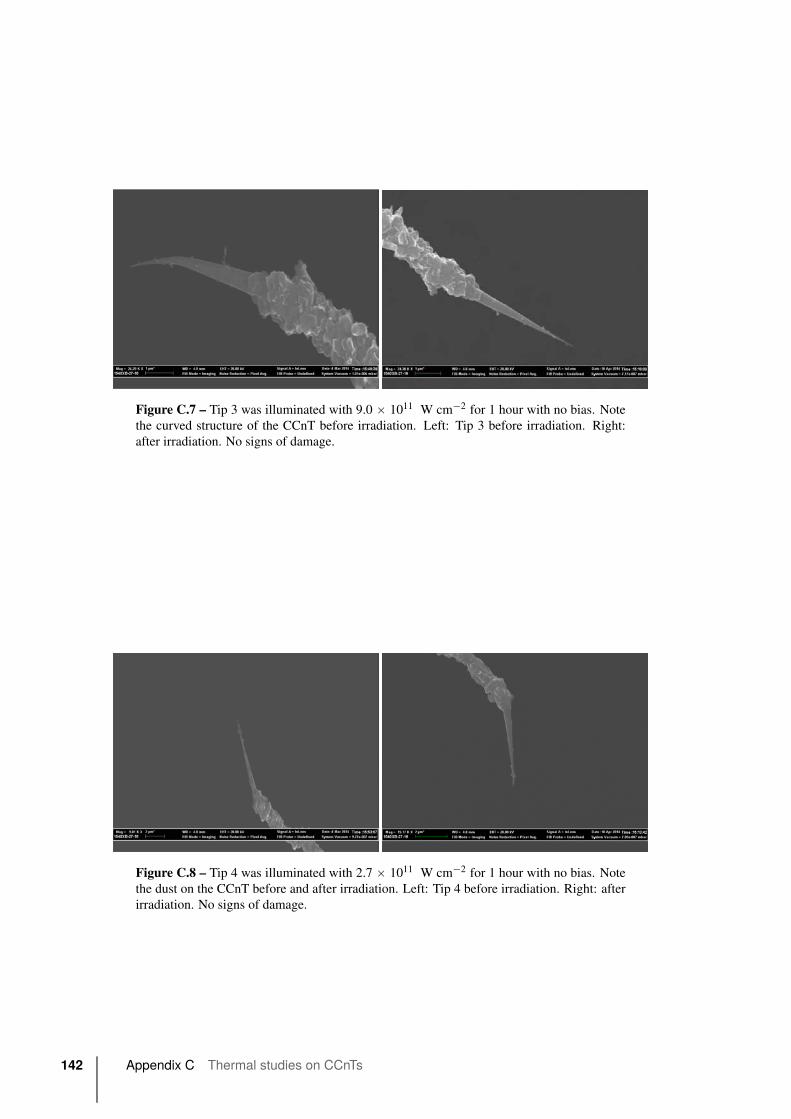
Figure C.7 – Tip 3 was illuminated with 9.0 ˆ 1011 W cm´2 for 1 hour with no bias. Note
the curved structure of the CCnT before irradiation. Left: Tip 3 before irradiation. Right:
after irradiation. No signs of damage.
Figure C.8 – Tip 4 was illuminated with 2.7 ˆ 1011 W cm´2 for 1 hour with no bias. Note
the dust on the CCnT before and after irradiation. Left: Tip 4 before irradiation. Right: after
irradiation. No signs of damage.
142 Appendix C Thermal studies on CCnTs
DRésumé en français
Introduction
L’émission d’électrons d’un matériau est un problème fondamental de physique d’un grand
intérêt. Comprendre les mécanismes induisant l’émission d’un électron est utile pour la com-
préhension des propriétés des matériaux mais aussi des processus d’interaction. Historique-
ment, le processus d’émission d’électrons par la lumière, l’effet photoélectrique [Einstein05],
est intéressant grâce à ses applications potentielles. Avec l’arrivée des lasers, la photoémission
d’électrons à partir d’une surface métallique a été systématiquement étudié [Lee73, Venus83].
Cela a conduit à l’étude de la physique des interactions entre la lumière et la matière et les phé-
nomènes qui en découlent. Les applications potentielles comprennent des sources d’électrons
pour la microscopie, des accélérateurs et des lasers à électrons libres.
Pour étendre les études de l’interaction lumière-matière en champ fort réalisées sur des sys-
tèmes en phase solide (macroscopique) ou gazeuse (microscopique), des nanopointes métal-
liques sont utilisées. Ces échantillons bénéficient de l’amplification locale du champ par effet
de pointe. Cela signifie que le champ optique appliqué par le laser est amplifié en raison de la
forme de l’échantillon, ce qui permet de diminuer la puissance laser nécessaire pour atteindre
ce régime de champ fort. Les nanopointes peuvent être utilisées comme sources d’impulsions
ultracourtes d’électrons avec une cohérence spatiale et temporelle élevée pour une utilisation
dans des expériences d’onde de la matière [Barwick08]. Cela a des applications directes pour
l’imagerie femtoseconde et sources de diffraction électronique aux temps courts.
Ma thèse concerne l’étude des mécanismes physiques qui conduisent à l’émission photo-
assistée d’électrons par des impulsions laser ultracourtes à partir d’une nanopointe. Ceci est
une nouvelle direction ’ pour mon équipe et mon travail inclut donc le développement com-
plet d’une nouvelle expérience pour observer et identifier ces mécanismes d’émission. Avant
mon arrivée, la recherche de notre groupe était centrée sur des développements expérimentaux
de protocoles de contrôle cohérent en utilisant des impulsions ultracourtes mises en forme
[Monmayrant10] sur différents systèmes des atomes aux molécules aux boîtes quantiques,
ainsi que dans les milieux diffusants [McCabe11]. Cette expertise dans le développement de
source laser et des techniques de contrôle ajoute des paramètres que nous pouvons utiliser pour
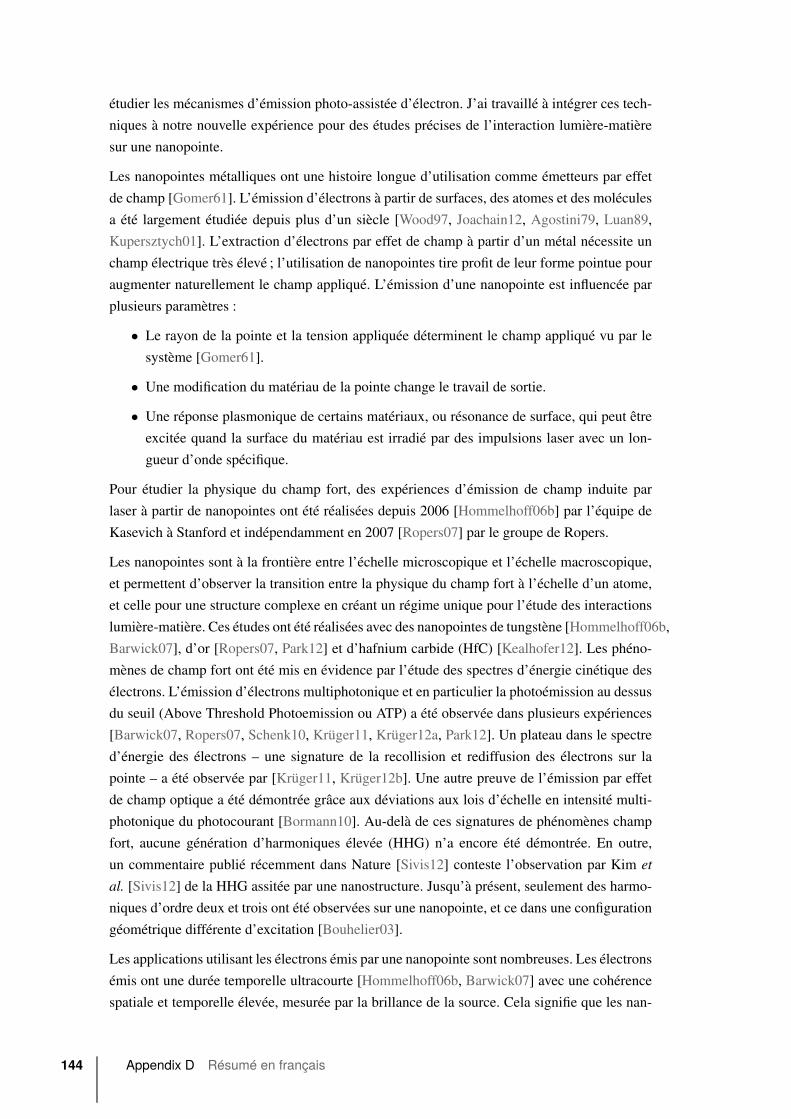
étudier les mécanismes d’émission photo-assistée d’électron. J’ai travaillé à intégrer ces tech-
niques à notre nouvelle expérience pour des études précises de l’interaction lumière-matière
sur une nanopointe.
Les nanopointes métalliques ont une histoire longue d’utilisation comme émetteurs par effet
de champ [Gomer61]. L’émission d’électrons à partir de surfaces, des atomes et des molécules
a été largement étudiée depuis plus d’un siècle [Wood97, Joachain12, Agostini79, Luan89,
Kupersztych01]. L’extraction d’électrons par effet de champ à partir d’un métal nécessite un
champ électrique très élevé ; l’utilisation de nanopointes tire profit de leur forme pointue pour
augmenter naturellement le champ appliqué. L’émission d’une nanopointe est influencée par
plusieurs paramètres :
• Le rayon de la pointe et la tension appliquée déterminent le champ appliqué vu par le
système [Gomer61].
• Une modification du matériau de la pointe change le travail de sortie.
• Une réponse plasmonique de certains matériaux, ou résonance de surface, qui peut être
excitée quand la surface du matériau est irradié par des impulsions laser avec un lon-
gueur d’onde spécifique.
Pour étudier la physique du champ fort, des expériences d’émission de champ induite par
laser à partir de nanopointes ont été réalisées depuis 2006 [Hommelhoff06b] par l’équipe de
Kasevich à Stanford et indépendamment en 2007 [Ropers07] par le groupe de Ropers.
Les nanopointes sont à la frontière entre l’échelle microscopique et l’échelle macroscopique,
et permettent d’observer la transition entre la physique du champ fort à l’échelle d’un atome,
et celle pour une structure complexe en créant un régime unique pour l’étude des interactions
lumière-matière. Ces études ont été réalisées avec des nanopointes de tungstène [Hommelhoff06b,
Barwick07], d’or [Ropers07, Park12] et d’hafnium carbide (HfC) [Kealhofer12]. Les phéno-
mènes de champ fort ont été mis en évidence par l’étude des spectres d’énergie cinétique des
électrons. L’émission d’électrons multiphotonique et en particulier la photoémission au dessus
du seuil (Above Threshold Photoemission ou ATP) a été observée dans plusieurs expériences
[Barwick07, Ropers07, Schenk10, Krüger11, Krüger12a, Park12]. Un plateau dans le spectre
d’énergie des électrons – une signature de la recollision et rediffusion des électrons sur la
pointe – a été observée par [Krüger11, Krüger12b]. Une autre preuve de l’émission par effet
de champ optique a été démontrée grâce aux déviations aux lois d’échelle en intensité multi-
photonique du photocourant [Bormann10]. Au-delà de ces signatures de phénomènes champ
fort, aucune génération d’harmoniques élevée (HHG) n’a encore été démontrée. En outre,
un commentaire publié récemment dans Nature [Sivis12] conteste l’observation par Kim etal. [Sivis12] de la HHG assitée par une nanostructure. Jusqu’à présent, seulement des harmo-
niques d’ordre deux et trois ont été observées sur une nanopointe, et ce dans une configuration
géométrique différente d’excitation [Bouhelier03].
Les applications utilisant les électrons émis par une nanopointe sont nombreuses. Les électrons
émis ont une durée temporelle ultracourte [Hommelhoff06b, Barwick07] avec une cohérence
spatiale et temporelle élevée, mesurée par la brillance de la source. Cela signifie que les nan-
144 Appendix D Résumé en français
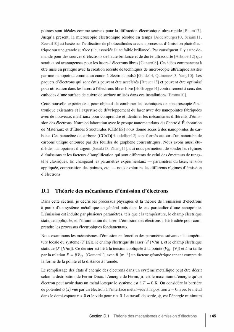
pointes sont idéales comme sources pour la diffraction électronique ultra-rapide [Baum13].
Jusqu’à présent, la microscopie électronique résolue en temps [Aidelsburger10, Sciaini11,
Zewail10] est basée sur l’utilisation de photocathodes avec un processus d’émission photoélec-
trique sur une grande surface (i.e. associée à une faible brillance). Par conséquent, il y a une de-
mande pour des sources d’électrons de haute brillance et de durée ultracourte [Arbouet12] qui
serait aussi avantageuses pour les lasers à électrons libres [Ganter08]. Ces idées commencent à
être mise en pratique avec la création récente de techniques de microscopie ultrarapide assitée
par une nanopointe comme un canon à électrons pulsé [Gulde14, Quinonez13, Yang10]. Les
paquets d’électrons qui sont émis peuvent être accélérés [Breuer13] et peuvent être optimisé
pour utilisation dans les lasers à l’électrons libres libre [Hoffrogge14] contrairement à ceux des
cathodes d’une surface de cuivre de surface utilisés dans ces installations [Emma10].
Cette nouvelle expérience a pour objectif de combiner les techniques de spectroscopie élec-
tronique existantes et l’expertise de développement du laser avec des nanopointes fabriquées
avec de nouveaux matériaux pour comprendre et identifier les mécanismes différents d’émis-
sion des électrons. Notre collaboration avec le groupe nanomatériaux du Centre d’Élaboration
de Matériaux et d’Etudes Structurales (CEMES) nous donne accès à des nanopointes de car-
bone. Ces nanocône de carbone (CCnT)[Houdellier12] sont formés autour d’un nanotube de
carbone unique entourée par des feuilles de graphène concentriques. Nous avons aussi étu-
dié des nanopointes d’argent [Sasaki13, Zhang11], qui nous permettent de sonder les régimes
d’émissions et les facteurs d’amplification qui sont différents de celui des émetteurs de tungs-
tène classiques. En changeant les paramètres expérimentaux — paramètres du laser, tension
appliquée, composition des pointes, etc. — nous explorons les différents régimes d’émission
d’électrons.
D.1 Théorie des mécanismes d’émission d’électrons
Dans cette section, je décris les processus physiques et la théorie de l’émission d’électrons
à partir d’un système métallique en général puis dans le cas particulier d’une nanopointe.
L’émission est induite par plusieurs paramètres, tels que : la température, le champ électrique
statique appliquée, et l’illumination du laser. L’émission des électrons a été étudiée pour com-
prendre les processus électroniques fondamentaux.
Nous examinons les mécanismes d’émission en fonction des paramètres suivants : la tempéra-
ture locale du système (T [K]), le champ électrique du laser (E [V/m]), et le champ électrique
statique (F [V/m]). Ce dernier est lié à la tension appliquée à la pointe (Vtip [V]) et à sa taille
par la relation F “ βVtip [Gomer61], avec β [m´1] un facteur géométrique tenant compte de
la forme de la pointe et la distance à l’anode.
Le remplissage des états d’énergie des électrons dans un système métallique peut être décrit
selon la distribution de Fermi-Dirac. L’énergie de Fermi, μ , est le maximum d’énergie qu’un
électron peut avoir dans un métal lorsque le système est à T “ 0 K. On considère la barrière
de potentiel Upxq vue par un électron à l’interface métal-vide à la position x“ 0, avec le métal
dans le demi-espace xă 0 et le vide pour xą 0. Le travail de sortie, φ , est l’énergie minimum
Section D.1 Théorie des mécanismes d’émission d’électrons 145
nécessaire pour arracher un électron d’un système métallique. Ceci est équivalent a l’énergie
d’ionisation nécessaire pour arracher un électron d’un système atomique ou moléculaire. Si les
états électroniques sont pleins jusqu’à l’énergie de Fermi, φ représente l’énergie minimale que
le système doit absorber pour qu’un électron puisse être arraché du métal. Le travail de sortie
dépend du matériau et de son orientation (les différentes facettes d’une structure cristalline ont
chacune un travail de sortie différent) ainsi que l’état de surface (des molécules adsorbées et
la propreté de la surface).
Les processus d’émission sont résumés sous forme graphique dans la figure Fig. D.1. Quand on
modifie les paramètres appliqués à notre système (tension appliquée Vtip, intensité du laser I,énergie des photons hω , composition et rayon r de la nanopointe), on peut changer le processus
d’émission dominant qu’on observe.
Figure D.1 – Schéma montrant les mécanismes pour l’émission d’un électron induite par
laser à partir d’une interface métal-vide. Le niveau d’énergie de Fermi est μ , et la distribution
de Fermi-Dirac est représentée schématiquement en gris à basse température et en rouge à
température plus élevée. L’interface métal/vide est située à x “ 0 et le potentiel Upxq vu par
les électrons pour xą 0 est représenté en bleu. (a) Émission par effet de champ (flèche verte
en pointillés) et émission thermique ou thermoionique (flèche noire). Ces mécanismes ne
nécessitent pas d’illumination laser. (b) Processus d’émission à faible illumination laser. Les
impulsions laser peuvent être considérés du point de vue photonique. Si un nombre suffisant
de photons sont absorbés, un électron peut s’échapper au-dessus de la barrière de potentiel
(flèches noires), sinon un électron peut être émis par l’intermédiaire d’effet tunnel assisté par
absorption d’un photon ou d’absorption thermique de l’énergie d’un photon (flèche verte en
pointillés). (b) Aux intensités laser élevées, le champ laser modifie la barrière de potentiel
lui-même et peut émettre des électrons par effet tunnel optique.
Il existe plusieurs mécanismes à l’origine de l’émission d’électrons à partir de nanopointe, en
fonction du champ appliqué et l’intensité induite par laser sur le système. Fig. D.1 montre ces
mécanismes d’émission. La distribution en énergie des électrons à basse température est repré-
sentée en gris, avec le niveau de Fermi, μ , marqué par une ligne jaune. La redistribution des
énergies de Fermi due aux effets thermiques est représenté en rouge. L’interface métal/vide
est située à x “ 0. La Fig. D.1 (a) représente le cas sans laser. Le système peut être chauffé
tel que les électrons peuvent obtenir une énergie suffisante pour surmonter la barrière de po-
tentiel (flèche noire). C’est l’émission thermo-ionique décrite par l’équation de Dushman-
Richardson. En appliquant un champ électrique externe suffisant, la barrière est modifié donc
un électron peut passer à travers par effet tunnel (flèche verte en pointillés). C’est l’émission
de champ décrite par l’équation de Fowler Norheim. Dans Fig. D.1 (b), les impulsions laser
peuvent être considérées à partir de point de vue photonique. Ici, le laser a une intensité modé-
rée et un champ externe faible à modéré peut être appliqué au système. Si un nombre suffisant
146 Appendix D Résumé en français
de photons sont absorbés, un électron peut s’échapper au dessus de la barrière de potentiel
(émission au dessus du seuil, flèche noire). Sinon, un électron peut être émis par l’intermé-
diaire de l’effet tunnel assisté par l’absorption d’un photon (que nous appelons ici émission de
champ photonique) ou à partir d’un niveau d’énergie plus élevé peuplé par chauffage laser du
gaz d’électrons (émission de champ thermique). Aux intensités laser suffisamment élevées, le
champ laser lui-même modifie la barrière de potentiel permettant l’émission d’un électron par
effet tunnel pendant une fraction de cycle optique (Fig. D.1 (c)).
Les phénomènes d’émission laser décrits jusqu’à présent sont valables pour les systèmes ato-
miques et les surfaces métalliques [Joachain12], mais on doit considère le fait que dans cette
thèse, on regarde le photoémission à partie des systèmes d’une nanopointe. En tant que tel,
la géométrie de ces systèmes doit être prise en compte quand on considère le champ statique
appliqué ainsi que le champ optique du laser.
Le champ optique d’un laser est fortement affecté par les nanostructures. En particulier, on
parle de champ proche optique lorsque la longueur d’onde de la lumière est supérieure à la
taille de l’objet. Une localisation forte des champs se produit à proximité des structures et en
particulier de leurs extrémités. Typiquement nos nanopointes ont un rayon de l’ordre de „10-
100 nm de diamètre, beaucoup plus petit que la longueur d’onde du laser (800 nm) qui est
généralement utilisé.
Il y a trois raisons principales pour l’augmentation d’un champ optique [Thomas13] :
1. Une augmentation du champ géométrique provoquée par le discontinuité du constante
diélectrique à l’interface métal/vide. Cela conduit à une accumulation de charge sous
la surface qui crée un champ fort local en raison de la petite taille de la structure du
nanoobjet. Ceci est analogue à l’effet de paratonnerre électrostatique.
2. Une résonance d’antenne qui se produit dans des structures dont la taille est un multiple
impair de la moitié de la longueur d’onde [Thomas13, Krüger13].
3. Des effets plasmoniques dans des matériaux comme l’argent ou l’or. qui peuvent avoir
une résonance des électrons de surface lorsque la fréquence optique est proche de la
fréquence de résonance du plasmon [Sasaki13, Stockman11]. Ces résonances sont très
dépendantes du matériau, de la forme du nanoobjet et de la longueur d’onde appliquée.
Cela signifie que les intensités laser typiquement nécessaires pour atteindre le régime de champ
fort peuvent être réduites grâce à l’amplification du champ optique, ce qui ne rend plus néces-
saire l’utilisation d’une chaine laser amplifiée.
D.2 Dispositifs optiques et développement d’un NOPA
Dans cette section, je décris le système optique développé et utilisé pendant ma thèse. Pour
étudier l’émission d’électrons à partir de nanopointe induite par un champ laser, ce système
doit remplir certaines conditions. On a besoin d’une durée d’impulsion courte pour obtenir une
puissance crête associée élevée mais sans avoir une puissance moyenne élevée, et ainsi éviter
les effets thermiques créés par le laser. On voudrait également une haute cadence du laser pour
Section D.2 Dispositifs optiques et développement d’un NOPA 147

avoir le meilleur rapport signal sur bruit possible car l’utilisation d’un objet unique ne permet
pas de détecter plus d’un électron par impulsion laser. Le système laser que nous avons uti-
lisé est passé par beaucoup évolution au cours de ma thèse : oscillateur femtoseconde, chaine
laser amplifiée, et développement d’une nouvelle source à partir d’un laser femtoseconde fi-
bré.
Figure D.2 – (a) La sortie directe de l’oscillateur peut être précisément contrôlée et envoyée
vers l’expérience (b) ou peut être amplifiée en énergie et avec un taux de répétition réduit. (c)
Le contrôle précis de la polarisation et de l’énergie déposée sur la pointe est crucial pour l’ex-
périence. Un cristal non-linéaire facultatif peut être inséré dans le faisceau pour le doublage
de fréquence la lumière. TFP : polariseur de couche mince, SPIDER : dispositif de mesure
de la durée des impulsions décrit dans Sec 2.2
Nous avons mis en place un système laser flexible complètement caractérisable et contrôlable.
Le premier système de laser est basé sur un oscillateur Ti :saphir classique de 800 nm qui peut
aussi être utilisé dans une chaîne d’ampflication. Avec ce système, nous avons la possibilité de
basculer entre un mode du puissance moyenne modérée, avec une haute cadence à 62 MHz,
ainsi que un mode du puissance moyenne faible, avec une basse cadence de 1 kHz, avec la
même intensité crête pour les deux modes. On a aussi la possibilité de doubler la fréquence de
la sortie du laser pour produire des impulsions à 400 nm.
Un oscillateur femtoseconde commercial standard de Titane-saphir, "Femtolaser femotsource
synergy", est la source de laser primaire pour les expériences à haute cadence. L’oscillateur a
un taux de répétition de 62 MHz, avec une longueur d’onde centrale de 800 nm et une bande
passante spectrale de largeur environ 70 nm à mi-hauteur (fwhm) correspondant à une durée
d’impulsion de „20 fs. La puissance moyenne totale disponible à la sortie de l’oscillateur est
„ 360 mW ce qui correspond à une énergie par impulsion de 5,8 nJ.
Quand on utilise le faisceau de l’oscillateur (Fig. D.2 (a)), l’énergie d’impulsion (ou puis-
sance moyenne), la polarisation, la durée et la dispersion (chirp) sont attentivement réglées et
contrôlées pendant toute l’expérience. La dispersion inhérente de l’oscillateur ainsi que toute
dispersion supplémentaire ajoutée par les matériaux optiques et le hublot de la chambre expé-
148 Appendix D Résumé en français
rimentale sont mesurées avec un SPIDER (décrit dans Sec. 2.2) et pré-compensées avec des
paires de miroirs à dispersion négative. La puissance est réglée avec une lame demi-onde et
un polariseur de couche mince (TFP) avec un taux d’extinction de „ 200 :1. La polarisation
du faisceau est nettoyée avec un autre polariseur TFP et ensuite choisie avec une lame demi-
onde avant que les impulsions laser ne soient envoyées vers l’expérience. Pour minimiser la
dispersion et maintenir la durée courte des impulsions, toutes les optiques utilisées sont réflé-
chissantes quand cela était possible (miroirs plans et sphériques, etc.), et sinon, le plus mince
possible (polariseurs TFP, lame demi-onde d’ordre 0 (femtolaser), etc.).
Alternativement, la sortie de l’oscillateur peut être envoyée vers la chaine d’amplification (am-
plificateur régénératif ou regen) (Fig. D.2 (b)). Un regen marche d’une manière similaire à une
cavité laser [Barty96, Wynne94]. Pendant l’étape d’amplification, les impulsions de quelques
femtosecondes générées à partir de l’oscillateur sont étirées temporellement jusqu’à quelques
centaines de picosecondes. L’impulsion étirée de faible énergie, est injectée dans la cavité en
utilisant une cellule de Pockels et fait plusieurs allers-retours à travers le milieu à gain (géné-
ralement Ti :saphir). Enfin, elle sort de la cavité par une autre cellule de Pockels. L’impulsion
de haute énergie est ensuite recomprimée jusqu’à sa durée limitée par transformée de Fourier.
Cela nous permet d’avoir des impulsions avec une énergie de l’ordre de 350 μJ, avec un taux
de répétition de 1 kHz, et une durée des impulsions autour de 40 fs, avec une limite de Fourier
de 35 fs. Bien que seuls quelques nJ d’énergie soient nécessaires pour l’émission d’électrons
à partir de nanopointe, les impulsions de plus haute énergie pourraient nous permettre de ma-
nipuler les impulsions avec des dispositifs de mise en forme temporelle et de conversion en
longueur d’onde. Le taux de répétition relativement bas permet de s’affranchir des effets ther-
miques potentiels dans la nanopointe, dus au dépôt de puissance moyenne modérée.
Table D.1 – Résumé des caractéristiques des différents modes defonctionnement du laser utilisés et
accessibles pour l’expérience.
taux de longueur bande durée énergie puissancerépétition d’onde passante impulsion d’impulsion (avant crête (avant(R) centrale spectrale compresseur) la chambre)
oscillateur 62 MHz 800 nm 70 nm 20 fs 5.8 nJ 1.9 ˆ105 W
Regen 1 kHz 800 nm 30 nm 40 fs 350 μJ 5.3 ˆ109 W
NOPA 1 kHz – 700 nm 44 nm 45 fs low R : 0.27 μJ 1.7 ˆ106 W
(now) 1 MHz high R : 14 nJ 8.8 ˆ105 W
750 nm 67 nm 40 fs low R : 0.15 μJ 9.4 ˆ105 W
high R : 11 nJ 6.9 ˆ104 W
800 nm 84 nm 35 fs low R : 0.08 μJ 5.0 ˆ105 W
high R : 4 nJ 2.5 ˆ104 W
NOPA single shot – 700-850 nm „100 nm „10 f 10s nJ „ 105 W
(ideal) 2 MHz
Pour pouvoir étudier plus précisément les effets du taux de répétition et de la longueur d’onde
sur l’émission d’électrons dans la nanopointes, nous avons acquis un système laser fibré in-
frarouge (1030 nm) qui permet une variabilité des taux de répétition, du tir unique à plusieurs
dizaines de MHz, tout en conservant la même puissance crête (Tangerine, Amplitude Sys-
tèmes). L’inconvénient d’un tel système est la longue durée d’impulsion, de 300 fs. Pour avoir
Section D.2 Dispositifs optiques et développement d’un NOPA 149
accès à la courte durée d’impulsion nécessaire, nous avons construit un étage d’amplification
paramétrique optique non colinéaire (NOPA) à la sortie [Cerullo03]. Cette source laser a deux
possibilités de réglage fin en longueur d’onde et en taux de répétition, ainsi qu’une sortie de
puissance suffisante de de courte durée.
Un résumé des caractéristiques des impulsions pour les différents modes laser se trouve dans
Tab. D.1.
D.3 Dispositif expérimental
La nanopointe est montée dans une chambre à ultra-vide (UHV) et éclairée par une source laser
ultracourte très focalisée décrite dans la section précédente et dans le chapitre 2. Les électrons
émis sont ensuite détectés avec un spectromètre d’électrons à champ retardé, avec la possibi-
lité d’une détection résolue spatialement. Cette configuration a été entièrement développée au
cours de mon travail de thèse. Le dispositif expérimental a subi plusieurs évolutions pendant
ma thèse. D’une manière générale, la configuration est très polyvalente, et utilise de nombreux
éléments différents : lasers, manipulation nanométrique de la nanopointe détection d’électrons,
technologies sous vide et logiciels fait maison pour l’acquisition de données.
Pour la recherche de ma thèse, j’ai utilisé 3 types de nanopointes : nanopointes de tungs-
tène que j’ai fabriquée au CEMES ; cônes de carbone qui ont été faites au CEMES par Au-
rélien Masseboeuf ; nanopointes et d’argent qui ont été faites par Ivan Blum au GPM de
Rouen.
Chaque pointe nécessite une procédure de montage différente dans notre chambre à ultravide.
Les pointes sont positionnées dans la focalisation du laser avec des platines de translation na-
nométriques dans les trois dimensions. Les électrons émis sont détectés dans un spectromètre à
champ retardé fabriqué au laboratoire avec une résolution relative de„ 5ˆ10´2, et une trans-
mission de „ 60 %. Cet appareil nous permet de récupérer des spectres d’électrons intégrés
à partir desquels nous pouvons résoudre l’énergie cinétique des électrons. Le spectromètre
peut aussi se déplacer dans les deux dimensions transverses grâce à des platines de translation.
Ceci permet des mesures résolues spatialement (similaires au « field emission microscopy »
FEM).
La version finale du montage expérimental est composée de :
• une paire de miroirs paraboliques pour focaliser le laser et le recollimater.
• des platines de nanopositionnement pour positionner la nanopointe dans le foyer du
laser.
• un spectrométre et diaphragme en cuivre à l’entrée. Ces éléments bougent ensemble
pour être alignés sous la pointe à l’emplacement d’émission maximale pour des mesures
de spectre d’électrons intégrée, et peuvent également être translatés pour faire une carte
2D d’émission des électrons
On peux voir un schéma du montage expérimental dans la figure D.3.
150 Appendix D Résumé en français
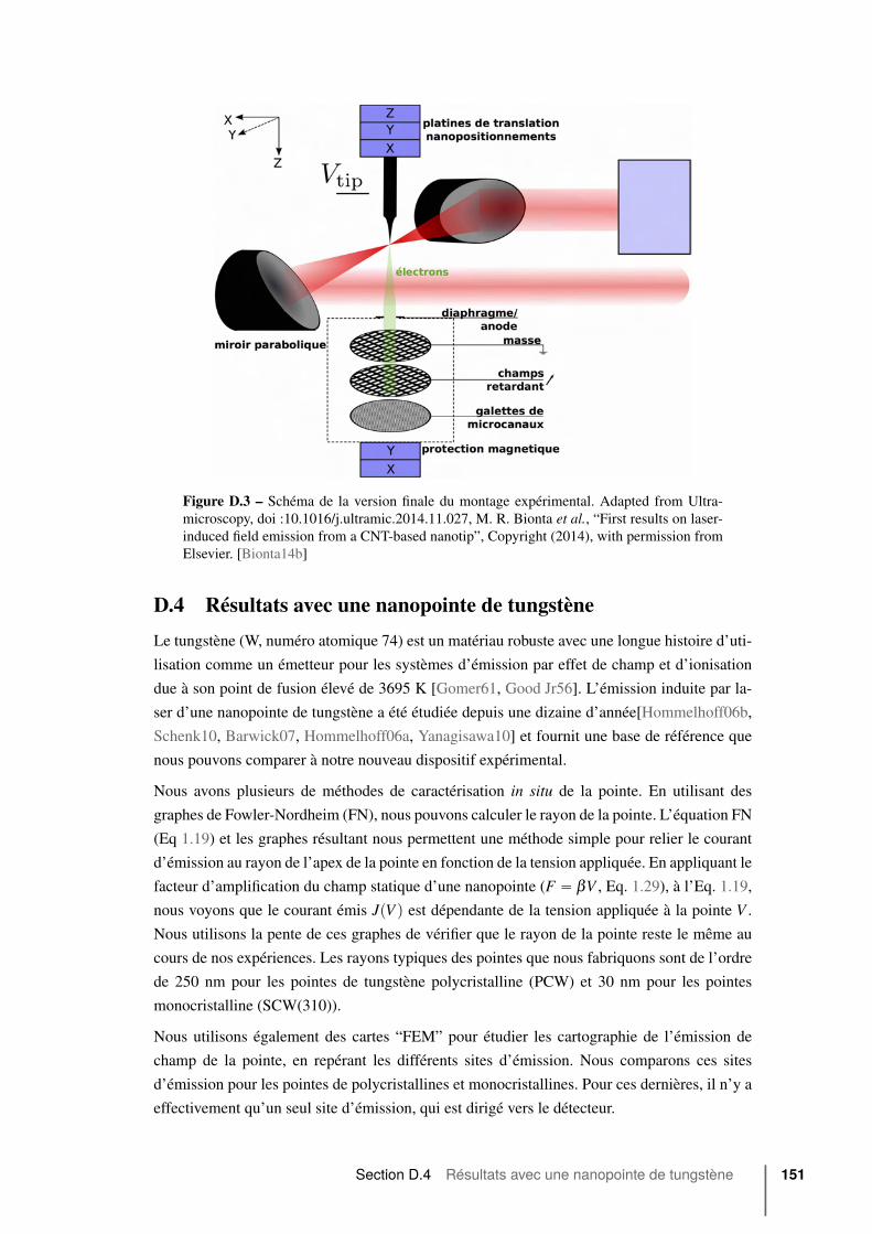
Figure D.3 – Schéma de la version finale du montage expérimental. Adapted from Ultra-
microscopy, doi :10.1016/j.ultramic.2014.11.027, M. R. Bionta et al., “First results on laser-
induced field emission from a CNT-based nanotip”, Copyright (2014), with permission from
Elsevier. [Bionta14b]
D.4 Résultats avec une nanopointe de tungstèneLe tungstène (W, numéro atomique 74) est un matériau robuste avec une longue histoire d’uti-
lisation comme un émetteur pour les systèmes d’émission par effet de champ et d’ionisation
due à son point de fusion élevé de 3695 K [Gomer61, Good Jr56]. L’émission induite par la-
ser d’une nanopointe de tungstène a été étudiée depuis une dizaine d’année[Hommelhoff06b,
Schenk10, Barwick07, Hommelhoff06a, Yanagisawa10] et fournit une base de référence que
nous pouvons comparer à notre nouveau dispositif expérimental.
Nous avons plusieurs de méthodes de caractérisation in situ de la pointe. En utilisant des
graphes de Fowler-Nordheim (FN), nous pouvons calculer le rayon de la pointe. L’équation FN
(Eq 1.19) et les graphes résultant nous permettent une méthode simple pour relier le courant
d’émission au rayon de l’apex de la pointe en fonction de la tension appliquée. En appliquant le
facteur d’amplification du champ statique d’une nanopointe (F “ βV , Eq. 1.29), à l’Eq. 1.19,
nous voyons que le courant émis JpV q est dépendante de la tension appliquée à la pointe V .
Nous utilisons la pente de ces graphes de vérifier que le rayon de la pointe reste le même au
cours de nos expériences. Les rayons typiques des pointes que nous fabriquons sont de l’ordre
de 250 nm pour les pointes de tungstène polycristalline (PCW) et 30 nm pour les pointes
monocristalline (SCW(310)).
Nous utilisons également des cartes “FEM” pour étudier les cartographie de l’émission de
champ de la pointe, en repérant les différents sites d’émission. Nous comparons ces sites
d’émission pour les pointes de polycristallines et monocristallines. Pour ces dernières, il n’y a
effectivement qu’un seul site d’émission, qui est dirigé vers le détecteur.
Section D.4 Résultats avec une nanopointe de tungstène 151

Le seuil de dommages des nanopointes à partir de l’irradiation du laser ont été empiriquement
étudié. Ces tests n’ont pas été concluants.
L’émission d’électrons induite par le laser est très dépendante de la polarisation. Nous avons
utilisé des courbes de dépendance de l’émission d’électrons en fonction de la polarisation
pour vérifier l’alignement de la pointe dans le foyer de focalisation du laser. En effet, l’émis-
sion par effet de champ photonique dépend uniquement de la composante du champ élec-
trique de laser qui est perpendiculaire de la surface [Venus83]. À l’apex de la pointe, il s’agit
de la composante parallèle à l’axe de la pointe. Par ailleurs, l’amplification du champ op-
tique, en raison de la taille du sous-longueur d’onde de la nanopointe, est plus grande pour
des polarisations parallèles à l’axe de la pointe. Par contre, l’émission d’électrons thermiques
induite par laser est plus efficace pour la polarisation perpendiculaire à l’axe de la pointe
[Barwick07, Hadley85].
Figure D.4 – Nombre d’électrons en fonction de la polarisation du laser (θ ) par rapport de
l’axe de la pointe. Les polarisations parallèles à l’axe de pointe (angles de polarisation de 0 et
90) conduisent à l’émission d’électrons la plus forte. Par contre, des polarisations perpendicu-
laires (angles de 180 et 270) ont des émissions négligeables. Les données expérimentales (x
bleus) sont ajustées à une courbe de la forme cos2npθq (ligne verte). Adapted with permission
from [Bionta14a].
La dépendance en polarisation d’une pointe bien alignée est décrite dans la dans la figure 4.6
[Bionta14a]. La production d’électrons maximale a lieu pour des angles de polarisation de 0
et 180, et est minimale à 90 et 270 et un contraste de „3500 : 1.
Pour des champs laser modérés, le courant d’électrons émis est proportionnel à l’intensité du
laser avec un exposant η (J 9 Iη , Eq. 1.26). Cela signifie que pour les régimes multiphoto-
niques (l’émission par effet de champ photonique et la photoémission au dessus du seuil ou
ATP), si le système absorbe n photons avant qu’un électron ne soit émis, nous nous attendons
à l’exposant η soit égale à n, où n est le nombre de photons absorbés. La moyenne d’éner-
gie des électrons sera alors η hω´φ . η est la moyenne des photons absorbé pour l’ensemble
des contributions des différents nombre de photons absorbés pour les électrons qui sont émis
152 Appendix D Résumé en français

par le système. La dépendance en puissance du laser nous donne donc le nombre moyen de
photons absorbés par le système avant l’émission d’électrons. Pour mesurer ce facteur η , on
fait varier l’intensité du laser de 3,8 à 11,4 ˆ1011 W cm´2 (puissance moyenne de 50 à 150
mW) avec Vtip = 50 V. Une dépendance exponentielle est clairement visible. En traçant en
échelle logarithmique, cela devient une relation linéaire à partir de laquelle nous pouvons faire
un ajustement linéaire. La pente de cette droite nous montre que η “ 2,9. Comme le tungs-
tène polycristallin (PCW) a un travail de sortie de φ “ 4,5 eV, et que l’énergie des photons
à 800 nm est 1,55 eV, nous voyons que le facteur η extrait est très proche de φ{hω “ 2,9,
en indiquant l’émission sur le seuil. Nous trouvons une diminution de ce nombre quand la
tension appliquée augmente, en raison de l’effet Schottky (réduction du travail de sortie du au
potentiel image en présence d’un champ statique appliqué). Nous pouvons également utiliser
les courbes de dépendance en polarisation pour déterminer ce facteur η à l’aide d’une courbe
d’ajustement du type cos2η θ . Dans la courbe de la figure 4.6, on trouve une valeur de 2,8 pour
cet exposant.
� � �� �����
���
���
���
���
���
��� �������
����
����������
����� ��
��
������� �
�
������������������
��������� �������������������
� � �� ���
�
�
�
�
�
������
��� �������
����
����������
������
������
�
������������������
��������� �������������������
Figure D.5 – Cela montre les spectres de photoélectrons à partir de nanopointe de W(310).
Pour ce spectre une tension d’extraction de Vtip = 20 V, et une puissance laser de 50 mW
(0,8 nJ/pulse, 1,52ˆ 1012 W cm´2 puissance crête) a été utilisé. La sortie du spectromètre
directe, une spectre intégré, est représentée par des points bleus. Le spectre de photoélectrons
résolu cinétiquement et représenté par la ligne verte. Remarquez que les pics d’ATP jusqu’à
l’ordre n “ 9 sont facilement observables dans le spectres/ L’insert montre les spectres en
échelle linéaire. Seuls les quatre premiers pics d’ATP sont facilement résoluble dans cette
échelle ; il est donc bénéfique pour tracer les spectres en échelle logarithmique.
Fig. D.5 montre un spectre de photoélectrons à partir de nanopointe W(310). Pour ce spectre
une tension d’extraction de Vtip = 20 V, et une puissance laser de 50 mW (0,8 nJ/pulse,
1,52ˆ 1012 W cm´2 puissance crête) ont été utilisées. L’énergie cinétique ajoutait de la
Vtip appliqué a été soustraite. L’insert de Fig. D.5 montre les spectres en échelle linéaire. Dans
le spectre de photoélectrons, les pics sont superposées sur la décroissance exponentielle glo-
Section D.4 Résultats avec une nanopointe de tungstène 153
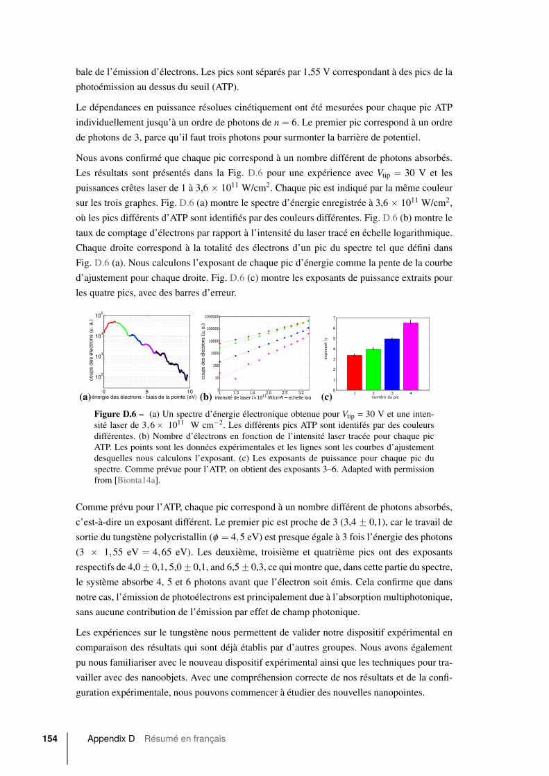
bale de l’émission d’électrons. Les pics sont séparés par 1,55 V correspondant à des pics de la
photoémission au dessus du seuil (ATP).
Le dépendances en puissance résolues cinétiquement ont été mesurées pour chaque pic ATP
individuellement jusqu’à un ordre de photons de n“ 6. Le premier pic correspond à un ordre
de photons de 3, parce qu’il faut trois photons pour surmonter la barrière de potentiel.
Nous avons confirmé que chaque pic correspond à un nombre différent de photons absorbés.
Les résultats sont présentés dans la Fig. D.6 pour une expérience avec Vtip “ 30 V et les
puissances crêtes laser de 1 à 3,6 ˆ 1011 W/cm2. Chaque pic est indiqué par la même couleur
sur les trois graphes. Fig. D.6 (a) montre le spectre d’énergie enregistrée à 3,6 ˆ 1011 W/cm2,
où les pics différents d’ATP sont identifiés par des couleurs différentes. Fig. D.6 (b) montre le
taux de comptage d’électrons par rapport à l’intensité du laser tracé en échelle logarithmique.
Chaque droite correspond à la totalité des électrons d’un pic du spectre tel que défini dans
Fig. D.6 (a). Nous calculons l’exposant de chaque pic d’énergie comme la pente de la courbe
d’ajustement pour chaque droite. Fig. D.6 (c) montre les exposants de puissance extraits pour
les quatre pics, avec des barres d’erreur.
0 5 10
102
103
104
105
énergie des électrons - biais de la pointe (eV)
co
up
s d
es é
lectr
on
s (
u.
a.)
(a) � ��� ��� ��� ��� ����
��
���
����
�����
������
�������
�� ����������������������� �����������
���������� ��������������
(b) � � � ��
�
�
�
�
�
�
�
������������
�������
�
(c)
Figure D.6 – (a) Un spectre d’énergie électronique obtenue pour Vtip = 30 V et une inten-
sité laser de 3,6ˆ 1011 W cm´2. Les différents pics ATP sont identifés par des couleurs
différentes. (b) Nombre d’électrons en fonction de l’intensité laser tracée pour chaque pic
ATP. Les points sont les données expérimentales et les lignes sont les courbes d’ajustement
desquelles nous calculons l’exposant. (c) Les exposants de puissance pour chaque pic du
spectre. Comme prévue pour l’ATP, on obtient des exposants 3–6. Adapted with permission
from [Bionta14a].
Comme prévu pour l’ATP, chaque pic correspond à un nombre différent de photons absorbés,
c’est-à-dire un exposant différent. Le premier pic est proche de 3 (3,4 ˘ 0,1), car le travail de
sortie du tungstène polycristallin (φ “ 4,5 eV) est presque égale à 3 fois l’énergie des photons
(3 ˆ 1,55 eV “ 4,65 eV). Les deuxième, troisième et quatrième pics ont des exposants
respectifs de 4,0˘ 0,1, 5,0˘ 0,1, and 6,5˘ 0,3, ce qui montre que, dans cette partie du spectre,
le système absorbe 4, 5 et 6 photons avant que l’électron soit émis. Cela confirme que dans
notre cas, l’émission de photoélectrons est principalement due à l’absorption multiphotonique,
sans aucune contribution de l’émission par effet de champ photonique.
Les expériences sur le tungstène nous permettent de valider notre dispositif expérimental en
comparaison des résultats qui sont déjà établis par d’autres groupes. Nous avons également
pu nous familiariser avec le nouveau dispositif expérimental ainsi que les techniques pour tra-
vailler avec des nanoobjets. Avec une compréhension correcte de nos résultats et de la confi-
guration expérimentale, nous pouvons commencer à étudier des nouvelles nanopointes.
154 Appendix D Résumé en français
D.5 Résultats avec un nanocône de carbone
L’investigation de l’émission d’électrons à partir de nouveaux matériaux comme les nano-
tubes de carbone a donné des propriétés intéressantes pour l’émission par effet de champ. Ces
nouveaux échantillons ont une structure et des propriétés électroniques très différentes des
nanopointes métalliques classiques. Nous avons utilisé ces nanopointes car elles ont démon-
tré des propriétés mécaniques et électriques excellentes pour l’émission par effet de champ.
Elles sont donc prometteuses pour l’observation du phénomène de champ fort en résultant de
l’interaction laser-pointe.
Notre collaboration avec CEMES nous permet d’accéder à ce nouveau type de nanopointe
formée autour d’un nanotube de carbone unique, entouré de feuilles de graphène concentriques
pour former une forme conique. Ces pointes sont appelées nanocônes de carbone (Carbon
Cone nanoTip, CCnT). Des études vastes sur les émission par effet de champ à partir de ces
pointes peuvent être trouvés dans [deKnoop14, Houdellier12, Houdellier15]. Les mécanismes
à l’origine de l’émission d’électrons à partir de ces pointes sont inconnus et nous étudions les
propriétés de l’émission induite par laser de ces nanopointes à base de carbone.
Nos collaborateurs du CEMES se concentrent sur la synthèse des pointes ainsi que l’étude
des propriétés d’émission par effet de champ dans l’objectif d’utiliser ces pointes comme une
source d’électrons pour la microscopie électronique. Notre groupe vise à étudier l’interaction
d’une telle pointe avec un champ laser pour étudier les propriétés des émissions induites par
laser à partir d’une CCnT.
Le CCnT est une pointe basée sur une forme conique de carbone. Ces pointes ont un travail de
sortie de φ “ 5 eV [Houdellier12], et un diamètre d’apex de quelques nm. Le centre du cône
est un nanotube de carbone multifeuilles (CNT) unique, entourée par des feuilles de graphène
concentriques pour donner une forme conique. Le CNT central a un diamètre de„2 nm.
L’image de gauche de la figure D.7 montre la structure du nanocône. Comme décrit dans les
Secs. 3.1.2 et 5.1, les cônes sont initialement formés à chaque extrémité d’un court segment
de microfibre de carbone. Cette microfibre est fabriquée par un procédé de dépôt chimique
en phase vapeur développé au CEMES. Après avoir été coupée, la microfibre de carbone est
soudée sur une pointe de tungstène dans un FIB (Focused Ion Beam). Ce processus de déve-
loppement unique permet aux CCnT d’exposer certains paramètres qui sont importants pour
nos expériences. Cela comprend un ratio d’aspect élevé du CCnT, qui peut être plus pointu
que des pointes métalliques classiques tels que le tungstène ou l’or, et une taille d’apex plus
petite qui donne une amélioration de champ plus élevée au voisinage de la pointe.
Nous avons essayé d’utiliser des courbes de FN pour extraire le rayon de l’apex de nos CCnTs,
mais lla valeur obtenue n’était pas en accord avec la taille observée dans les images de SEM
et TEM. Ceci est probablement parce que les hypothèses utilisées pour l’amplification géo-
métrique et la fonction de Nordheim ne sont plus valables. Néanmois, nous pouvons toujours
utiliser la pente α{β des courbes de FN pour s’assurer que la pointe garde le même diamètre.
Les images FEM ont confirmé un site d’émission unique des CCnTs.
Nous avons donc étudié les effets de l’irradiation laser sur les CCnTs. Alors que les effets de
Section D.5 Résultats avec un nanocône de carbone 155

l’émission d’électrons étaient compréhensibles pour une faible puissance moyenne, nous avons
observé la destruction de la pointe à puissance moyenne modérée. Des études méthodiques sur
le seuil de dommage de CCnTs ont été effectuées. Nous avons observé des dommages pour
des pointes irradiées avec 9,0 ˆ 1011 W cm´2 pendant 30 minutes comme on le voit dans
le Fig. D.7. Mais, beaucoup de nos études systématiques ont été peu concluantes. Par la suite,
nous avons limité nos intensités laser à moins de 7,7 ˆ 1011 W cm´2.
Figure D.7 – L’image de gauche montre le CCnT avant l’irradiation du laser. L’image de
droite montre le même CCnT après avoir été éclairé par 7,7ˆ 1011 W cm´2 d’intensité
laser (0,48 nJ/impulsion, 30 mW puissance moyenne) pendant 30 minutes. Adapted from
Ultramicroscopy, doi :10.1016/j.ultramic.2014.11.027, M. R. Bionta et al., “First results on
laser-induced field emission from a CNT-based nanotip”, Copyright (2014), with permission
from Elsevier [Bionta14b].
À faible puissance laser, la dépendance de l’émission d’électrons par rapport à la polarisation
laser a donné un bon contraste et une courbe d’ajustement avec un exposant n = 3,4. Ceci
est en bon accord du nombre minimum de photons absorbés nmin “ 3,2 pour surmonter le
travail de sortie φ “ 5 eV du CCNT. Les spectres de photoélectrons pour des intensités laser
modérées ont des formes plus étroites que celles pour des intensités similaire sur le tungstène,
indiquant des effets thermiques possibles.
La figure D.8 montre un spectre d’électrons émis à partir d’un CCnT. Le CCnT était éclairé
avec une intensité laser modérée de 5,13ˆ1011 W cm´2 (0,3 nJ/impulsion, 20 mW puissance
moyenne), et une tensions appliquée sur la pointe Vtip de 50 V.
Même si l’exposant laser non linéaire indique une absorption de photons suffisamment pour
surmonter la fonction barrière de travail, ce spectre ne montre aucun signe de des pics de
photoémission au dessus du seuil. L’étroitesse du spectre indique que l’émission peut être
causée par des effets thermiques à haute cadence du laser comme l’émission par effet de champ
assistée thermiquement, ou des mécanismes plus complexes comme l’ATP à partir d’un gaz
d’électrons excités thermiquement dans lequel la température brouille la signature des pics
ATP (i.e. si kBT „ hω).
Nos essais d’augmenter l’intensité du laser pour mesurer la production des électrons en fonc-
tion de la puissance du laser pour extraire un η ont été infructueuses comme nous avons
endommagé la pointe.
Contrairement à nos hypothèses initiales sur les caractéristiques des CCnTs, il a donc été
difficile d’observer des phénomènes de champ fort à partir d’une interaction du laser avec
156 Appendix D Résumé en français

0.5 1 1.5 2 2.5 3 3.5 4 4.5 510
1
102
103
104
105
Énergie cinetique des électrons (eV)
co
up
s d
es
éle
ctr
on
s (
u.
a.)
Figure D.8 – Spectre d’énergie des photoélectrons émis d’un CCnT éclairé avec une intensité
laser modérée de 5,13ˆ1011 W cm´2 (0,3 nJ/impulsion, 20 mW puissance moyenne), et une
tensionVtip de 50 V. Adapted from Ultramicroscopy, doi :10.1016/j.ultramic.2014.11.027, M.
R. Bionta et al., “First results on laser-induced field emission from a CNT-based nanotip”,
Copyright (2014), with permission from Elsevier [Bionta14b].
un CCnT, en dépit de leurs meilleures propriétés mécaniques et électriques par rapport aux
nanopointes métalliques classiques. À faible puissance laser moyenne, les CCnTs émettent
de façon similaire à ce que nous avons observé avec des pointes de tungstène ; toutefois, les
hautes puissances moyennes ont conduit à une destruction des pointes. Nous avons envisagé les
explications suivantes sans être certains de leur validité. Bien que l’interface entre la fibre de
carbone et de la pointe de tungstène est supposée être une “soudure” tungstène, on ne connait
pas l’interface réelle entre le carbone et le tungstène, et cela pourrait se révéler un lien fragile et
sensible aux effets thermiques. Comme le cône lui-même est composé de feuilles de graphène,
la structure atomique des atomes de carbone qui forment la CCnT signifie qu’il y a moins
d’atomes de carbone constituant la pointe que dans une nanopointe de mêmes dimensions
fait en tungstène. Cela signifie qu’il y a plus d’énergie déposée par atome que par rapport à
des pointes tungstène. Une autre propriété inconnue de la CCnT peut aussi être un facteur
contribuant à son apparente fragilité.
Grâce au développement d’un NOPA (Sec. 2.3) avec une cadence variable et notre collabo-
ration active avec le CEMES vers la synthèse de nouveaux types de CCnTs, nous espérons
améliorer nos études sur l’émission laser d’électrons à partir des CCnTs. En particulier, la
forme de la pointe semble être cruciale pour la maximisation du processus d’émission.
Section D.5 Résultats avec un nanocône de carbone 157

D.6 Résultats avec une nanopointe d’argent
Nous avons étudié l’émission d’électrons à partir d’une nanopointe d’argent. L’argent (Ag,
numéro atomique 47) a une résonance connue de plasmon de surface autour de „400 nm, qui
est facilement accessible avec notre système de laser par doublage de fréquence. L’argent a un
point de fusion relativement faible de 1235 K et un travail de sortie de 4,25 eV [Haynes12]
pour sa forme polycristalline. C’est un métal noble avec une orbitale d complètement rempli et
1 électron dans l’orbitale s. En général l’or est préféré pour des études dans l’air en raison de
son inertie vis à vis de l’oxydation, mais l’argent peut être préférable dans le vide car il a moins
de pertes pour les longueurs d’onde visibles [Sasaki13]. L’argent est utilisé pour sa réponse
plasmonique forte et l’amplification de champ sur une large gamme de longueurs d’onde vi-
sibles [Schmid13] en raison de la petite composante imaginaire de sa constante diélectrique
[Zhang11, Johnson72]. Nous voulons voir comment cette résonance affecte l’émission d’élec-
trons et l’amélioration de champ optique.
Nous avons réalisé ces études en collaboration avec le GPM de Rouen.
Nous utilisons des pointes fabriquées dans un FIB avec un rayon connu de 20-50 nm. Le rayon
a été utilisé pour corroborer la fonction Nordheim utilisé avec les courbes de FN. Nous avons
également utilisé des images FEM pour observer les sites d’émission multiples dus à la nature
polycristalline des pointes.
0 5 10 1510
1
102
103
104
105
106
Énergie (eV)
co
up
s -
- e
ch
ell
e l
og
(u
. a
.)
1.52 × 10¹²
W cm−2
1.83 × 10¹²
W cm−2
2.13 × 10¹²
W cm−2
2.43 × 10¹²
W cm−2
2.74 × 10¹²
W cm−2
3.04 × 10¹²
W cm−2
3.65 × 10¹²
W cm−2
Figure D.9 – Spectres de photoélectrons pour des intensités laser de {1,52, 1,83, 2,13, 2,43,
2,74, 3,04, 3,65 } ˆ 1012 W cm´2, avec Vtip = 20 V. Les spectres sont plus étroits que ceux
obtenus à partir de nanopointes de tungstène avec des intensités équivalentes, mais avec une
émission beaucoup plus intense qui sature les MCPs. Ces effets de saturation ont été supprimé
des spectres.
Nous avons commencer par irradier la pointe avec une haute cadence. Nos premiers essais ont
eu des résultats imprévus que nous ne pouvions pas expliquer. Nous avons imagé la pointe
158 Appendix D Résumé en français
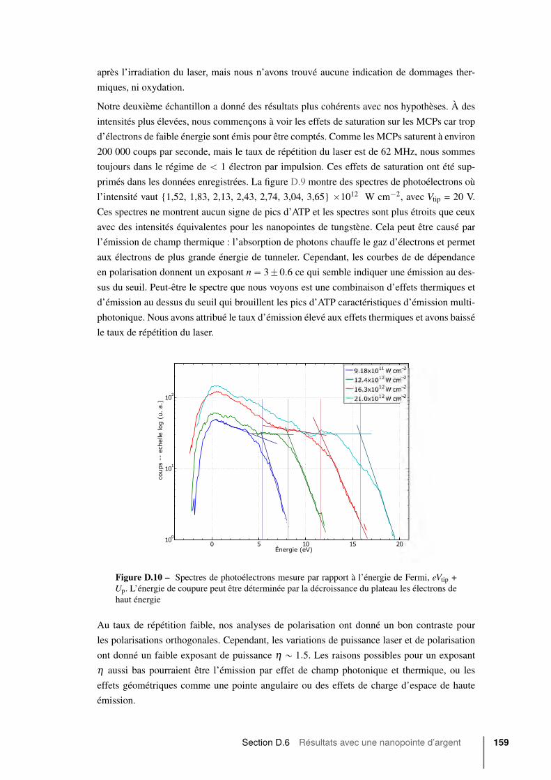
après l’irradiation du laser, mais nous n’avons trouvé aucune indication de dommages ther-
miques, ni oxydation.
Notre deuxième échantillon a donné des résultats plus cohérents avec nos hypothèses. À des
intensités plus élevées, nous commençons à voir les effets de saturation sur les MCPs car trop
d’électrons de faible énergie sont émis pour être comptés. Comme les MCPs saturent à environ
200 000 coups par seconde, mais le taux de répétition du laser est de 62 MHz, nous sommes
toujours dans le régime de ă 1 électron par impulsion. Ces effets de saturation ont été sup-
primés dans les données enregistrées. La figure D.9 montre des spectres de photoélectrons où
l’intensité vaut {1,52, 1,83, 2,13, 2,43, 2,74, 3,04, 3,65} ˆ1012 W cm´2, avec Vtip = 20 V.
Ces spectres ne montrent aucun signe de pics d’ATP et les spectres sont plus étroits que ceux
avec des intensités équivalentes pour les nanopointes de tungstène. Cela peut être causé par
l’émission de champ thermique : l’absorption de photons chauffe le gaz d’électrons et permet
aux électrons de plus grande énergie de tunneler. Cependant, les courbes de de dépendance
en polarisation donnent un exposant n“ 3˘0.6 ce qui semble indiquer une émission au des-
sus du seuil. Peut-être le spectre que nous voyons est une combinaison d’effets thermiques et
d’émission au dessus du seuil qui brouillent les pics d’ATP caractéristiques d’émission multi-
photonique. Nous avons attribué le taux d’émission élevé aux effets thermiques et avons baissé
le taux de répétition du laser.
� � �� �� �����
���
���
��� ������
��������� �
� �� � �������
�
����������� � �
Figure D.10 – Spectres de photoélectrons mesure par rapport à l’énergie de Fermi, eVtip +
Up. L’énergie de coupure peut être déterminée par la décroissance du plateau les électrons de
haut énergie
Au taux de répétition faible, nos analyses de polarisation ont donné un bon contraste pour
les polarisations orthogonales. Cependant, les variations de puissance laser et de polarisation
ont donné un faible exposant de puissance η „ 1.5. Les raisons possibles pour un exposant
η aussi bas pourraient être l’émission par effet de champ photonique et thermique, ou les
effets géométriques comme une pointe angulaire ou des effets de charge d’espace de haute
émission.
Section D.6 Résultats avec une nanopointe d’argent 159
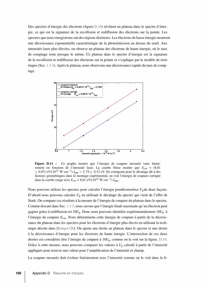
Des spectres d’énergie des électrons (figure D.10) révèlent un plateau dans le spectre d’éner-
gie, ce qui est la signature de la recollision et rediffusion des électrons sur la pointe. Les
spectres que nous enregistrons ont des régions distinctes. Les électrons de basse énergie montrent
une décroissance exponentielle caractéristique de la photoémission au dessus du seuil. Aux
intensités laser plus élevées, on observe un plateau des électrons de haute énergie, où le taux
de comptage reste presque le même. Ce plateau dans le spectre d’énergie est la signature
de la recollision et rediffusion des électrons sur la pointe et s’explique par le modèle de trois
étapes (Sec. 1.3.3). Après le plateau, nous observons une décroissance rapide du taux de comp-
tage.
0.8 1 1.2 1.4 1.6 1.8 2 2.25
10
15
20
Intensité appliquée ( × 1012
W cm−2
)
Én
erg
ie (
eV
)
coupure mesuréfit linéaire:E
cut= 8.8075 /10
12Iapp
− 2.7397
coupure corrigéfit corrigé: E
cut= 8.8075 /10
12Iapp
Figure D.11 – Ce graphe montre que l’énergie de coupure mesurée varie linéai-
rement en fonction de l’intensité laser. La courbe bleue montre que Ecut = (8,81
˘ 0.07) eV/(1012 W cm´2) Iapp “ 2,74˘ 0.52 eV. En corrigeant pour le décalage dû à des
facteurs géométriques dans le montage expérimental, on voit l’énergie de coupure corrigée
dans la courbe rouge avec Ecut = 8,81 eV/(1012 W cm´2) Iapp.
Nous pouvons utiliser les spectres pour calculer l’énergie pondéromotrice Upde deux façons.
D’abord nous pouvons calculer Up en utilisant le décalage du spectre qui vient de l’effet de
Stark. On compare ces résultats à la mesure de l’énergie de coupure du plateau dans le spectre.
Comme discuté dans Sec. 1.3.3, nous savons que l’énergie finale maximale qu’un électron peut
gagner grâce à rediffusion est 10Up. Donc nous pouvons identifier expérimentalement 10Up à
l’énergie de coupure Ecut. Nous déterminons cette énergie de coupure à partir de la décrois-
sance du plateau dans les spectres pour les électrons d’énergie plus élevés en utilisant la tech-
nique décrite dans [Krüger12b]. On ajuste une droite au plateau dans le spectre et une droite
à la décroissance d’énergie pour les électrons de haute énergie. L’intersection de ces deux
droites est considérée être l’énergie de coupure à 10Up, comme on le voit sur la figure. D.10.
Grâce à cette mesure, nous pouvons comparer les valeurs à Up calculé à partir de l’intensité
appliquée pour trouver une valeur pour l’amplification de l’intensité et champ.
La coupure mesurée doit évoluer linéairement avec l’intensité comme on le voit dans la fi-
160 Appendix D Résumé en français
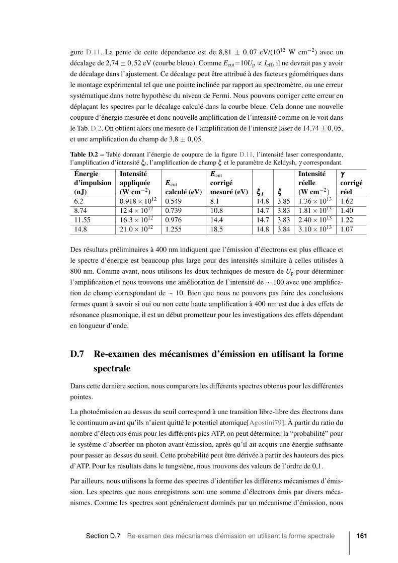
gure D.11. La pente de cette dépendance est de 8,81 ˘ 0,07 eV/(1012 W cm´2) avec un
décalage de 2,74˘ 0,52 eV (courbe bleue). Comme Ecut“10Up 9 Ieff, il ne devrait pas y avoir
de décalage dans l’ajustement. Ce décalage peut être attribué à des facteurs géométriques dans
le montage expérimental tel que une pointe inclinée par rapport au spectromètre, ou une erreur
systématique dans notre hypothèse du niveau de Fermi. Nous pouvons corriger cette erreur en
déplaçant les spectres par le décalage calculé dans la courbe bleue. Cela donne une nouvelle
coupure d’énergie mesurée et donc nouvelle amplification de l’intensité comme on le voit dans
le Tab. D.2. On obtient alors une mesure de l’amplification de l’intensité laser de 14,74˘ 0,05,
et une amplification du champ de 3,8 ˘ 0,05.
Table D.2 – Table donnant l’énergie de coupure de la figure D.11, l’intensité laser correspondante,
l’amplification d’intensité ξI , l’amplification de champ ξ et le paramètre de Keldysh, γ correspondant.
Énergie Intensité EEEcut Intensité γγγd’impulsion appliquée EEEcut corrigé réelle corrigé(nJ) (W cm´2) calculé (eV) mesuré (eV) ξξξ III ξξξ (W cm´2q réel6.2 0.918ˆ1012 0.549 8.1 14.8 3.85 1.36ˆ1013 1.62
8.74 12.4ˆ1012 0.739 10.8 14.7 3.83 1.81ˆ1013 1.40
11.55 16.3ˆ1012 0.976 14.4 14.7 3.83 2.40ˆ1013 1.22
14.8 21.0ˆ1012 1.255 18.5 14.8 3.84 3.10ˆ1013 1.07
Des résultats préliminaires à 400 nm indiquent que l’émission d’électrons est plus efficace et
le spectre d’énergie est beaucoup plus large pour des intensités similaire à celles utilisées à
800 nm. Comme avant, nous utilisons les deux techniques de mesure de Up pour déterminer
l’amplification et nous trouvons une amélioration de l’intensité de „ 100 avec une amplifica-
tion de champ correspondant de „ 10. Bien que nous ne pouvons pas faire des conclusions
fermes quant à savoir si oui ou non cette haute amplification à 400 nm est due à des effets de
résonance plasmonique, il est un début prometteur pour les investigations des effets dépendant
en longueur d’onde.
D.7 Re-examen des mécanismes d’émission en utilisant la formespectrale
Dans cette dernière section, nous comparons les différents spectres obtenus pour les différentes
pointes.
La photoémission au dessus du seuil correspond à une transition libre-libre des électrons dans
le continuum avant qu’ils n’aient quitté le potentiel atomique[Agostini79]. À partir du ratio du
nombre d’électrons émis pour les différents pics ATP, on peut déterminer la “probabilité” pour
le système d’absorber un photon avant émission, après qu’il ait acquis une énergie suffisante
pour passer au dessus du seuil. Cette probabilité peut être dérivée à partir des hauteurs des pics
d’ATP. Pour les résultats dans le tungstène, nous trouvons des valeurs de l’ordre de 0,1.
Par ailleurs, nous utilisons la forme des spectres d’identifier les différents mécanismes d’émis-
sion. Les spectres que nous enregistrons sont une somme d’électrons émis par divers méca-
nismes. Comme les spectres sont généralement dominés par un mécanisme d’émission, nous
Section D.7 Re-examen des mécanismes d’émission en utilisant la forme spectrale 161

pouvons identifier le processus physique basé sur la forme spectrale globale. Des informa-
tions sur les spécificités de chaque mécanisme derrière l’émission d’électrons peuvent être
obtenues pour chaque type de forme spectrale. Comme discuté dans les sections 6.4 et D.6,
l’augmentation de champ optique d’une pointe peut être mesurée à partir de l’observation d’un
plateau spectrale avec une comparaison de la mesure 10Up coupure avec la valeur attendue de
l’intensité appliquée.
Nous comparons les spectres de photoélectrons enregistrés pour diverses pointes avec la même
intensité crête du laser appliquée comme voir en Fig. D.12. Pour chaque pointe, le rayon est
environ le même (même ordre de grandeur, „ 30 nm), les travails de sortie sont similaires („5 eV), et les tensions appliquées sont du même ordre de grandeur („ 50 eV). Cela nous permet
de comparer les effets qui se produisent en raison des propriétés matériaux des pointes, guidant
à l’amplification de processus d’émission spécifique. Nous voyons un spectre plus étroit et le
manque de pics d’ATP pour une pointe d’argent et un CCnT à haute cadence (Fig. D.12, les
spectres bleus). On observe la photoémission multiphotonique pour SCW(310) avec des pics
dans le spectre (Fig. D.12, les spectres verts). Finalement, nous voyons des signes la recollision
et rediffusion des électrons sur la pointe dans le spectre de photoémission pour une pointe
d’argent à bas taux de répétition (Fig. D.12, les spectres rouges). Le taux de répétition du laser
a été baissé, donc la puissance moyenne est presque négligeable dans ce cas. Le spectre est
beaucoup plus large que ceux pour l’émission d’autres mécanismes. Il se forme un plateau à
des intensités plus élevées indiquant la recollision d’électrons.
Conclusion et perspectives
Dans cette thèse, j’ai présenté une nouvelle expérience pour étudier de l’émission des photo-
électrons induite par des impulsions laser ultracourtes à partir d’une nanopointe. Cette nouvelle
direction ’ pour mon groupe impliquait la conception complète et développement d’un nou-
veau dispositif expérimental incorporant des techniques de spectroscopie électronique exis-
tantes avec un expertise en développement du laser. Nous avons élargit les résultats exis-
tants dans les nanopointes métalliques classiques de tungstène [Hommelhoff06b, Barwick07,
Yanagisawa10] et or [Ropers07, Bormann10, Park12] en utilisant de nouvelles pointes inno-
vantes basées sur les nanotubes de carbone et de l’argent.
Cette thèse ne présente nullement une étude exhaustive sur le sujet de l’émission d’électrons à
partir nanopointe, ou même à partir de ces trois matériaux. Comme nous avons été limités par
des effets thermiques dans nos mécanismes d’émission, des investigations sur ces effets serait
utile pour des expériences de l’avenir. Il serait intéressant de voir à quel point les émissions
d’une nanopointe d’argent changent en fonction de la cadence des impulsions laser, de l’émis-
sion thermique à haute cadence aux effets de champ fort à cadence réduite. Cela permettrait
également de donner une échelle de temps pour la durée de états thermiques. Cet étude pourrait
être réalisée en examinant la forme spectrale émise en fonction de la cadence du laser ce qui
devient possible avec le développement du NOPA. Les mécanismes d’émission thermique ne
sont pas compris entièrement et des simulations sont nécessaires pour corroborer nos résultats
expérimentaux.
162 Appendix D Résumé en français

−2 0 2 4 6 8 10 12 140
1
2
3
4
5
6
Energie (eV)
Co
up
s -
- é
ch
ell
e lo
g, n
orm
ali
sé
Intensité crête du laser ∼6E11W cm−2
CC4 15 V, 20 mW, MHz
SCW 15 V, 20 mW, MHz
Ag 50 V, 8.74 nJ, kHz
0 5 10 15 200
1
2
3
4
5
6
Energie (eV)
Co
up
s -
- é
ch
ell
e lo
g, n
orm
ali
sé
Intensité crête du laser ∼1E12W cm−2
Ag 20 V, 50 mW, MHz
SCW 15 V, 50 mW, MHz
Ag 50 V, 14.8 nJ, kHz
Figure D.12 – Chaque ensemble de spectres a été enregistré avec la même intensité crête
du laser : en haut 6 ˆ 1011 W cm´2, en bas : 1 ˆ 1012 W cm´2. En changeant le matériau
de la pointe ou le taux de répétition du laser (puissance moyenne), on change le mécanisme
d’émission dominant. Les spectres bleus montrent des spectres plus étroits sans pics d’ATP,
indiquant des effets thermiques possibles. Les spectres verts montrent la photoémission mul-
tiphotonique caractérisée par des pics d’ATP séparé par l’énergie d’un photon. Les spectres
rouges montrent une transition dans le régime de l’effet tunnel optique avec un spectre plus
large et l’émergence un plateau, indiquant la recollision et rediffusion des électrons sur la
pointe.
Les investigations sur la réponse plasmonique d’un matériau pourraient conduire à des méca-
nismes d’émission dépendant de la longueur d’onde. Déjà des résultats préliminaires indiquent
qu’il y a une production d’électrons plus élevée et un spectre plus large pour un éclairage du
Section D.7 Re-examen des mécanismes d’émission en utilisant la forme spectrale 163
laser à proximité de la résonance de plasmon prédite théoriquement (pointe d’argent autour de
400nm). Des études systématiques sur la productions d’électrons en fonction de la longueur
d’onde proche de la résonance ou même la forme spectrale pourraient donner une vision de la
façon dont ces résonances affectent les propriétés électroniques de ces nanopointes.
La flexibilité de notre dispositif expérimental permet la possibilité de collecter la lumière laser
après son interaction avec la pointe. Comme effet tunnel optique, recollision et rediffusion des
électrons sont les mécanismes physiques à l’origine de la génération d’harmoniques élevée,
il est possible qu’avec quelques modifications de notre système, nous serions à même d’ob-
server des harmoniques provoquées par les pointes. Des expériences pompe-sonde pourraient
permettre de mesurer les propriétés des photoélectrons, et à l’aide de spectroscopie pompe-
sonde nous pourrions extraire les propriétés optiques de nos nanostructures. Enfin, l’émission
de pointes assistée par laser peut être utilisée pour étudier les propriétés fondamentales sur
les électrons tels que l’interférence électronique [Barwick08, Vidil] et pour des expériences
d’onde de matière.
L’expérience présentée dans cette thèse permet d’explorer les interactions lumière-matière
dans un régime unique entre la phase gazeuse de la physique atomique et la matière condensée
grâce à l’utilisation des nanopointes. L’émission d’électrons à partir d’une nanopointe exhibe
déjà des comportements de ces deux régimes, et la combinaison des expertises en physique
des lasers et en nanomatériaux pourra permettre d’étendre la physique du champ fort à ces
nouveaux systèmes au fort potentiel d’application.
164 Appendix D Résumé en français
References
[Agostini79] Agostini P, Fabre F, Mainfray G, Petite G and Rahman NK. Free-FreeTransitions Following Six-Photon Ionization of Xenon Atoms. Physical
Review Letters, 42 (17): 1127 (1979).
[Aidelsburger10] Aidelsburger M, Kirchner FO, Krausz F and Baum P. Single-electronpulses for ultrafast diffraction. Proceedings of the National Academy of
Sciences of the United States of America, 107 (46): 19714–19719 (2010).
[Allouche03] Allouche H,MonthiouxM and Jacobsen RL. Chemical vapor deposition ofpyrolytic carbon on carbon nanotubes Part 1. Synthesis and morphology.Carbon, 41 (15): 2897–2912 (2003).
[Allouche05] Allouche H and Monthioux M. Chemical vapor deposition of pyrolyticcarbon on carbon nanotubes. Part 2. Texture and structure. Carbon, 43 (6):
1265–1278 (2005).
[Arbouet12] Arbouet A, Houdellier F, Marty R and Girard C. Interaction of an ul-trashort optical pulse with a metallic nanotip: A Green dyadic approach.Journal of Applied Physics, 112 (5): 053103 (2012).
[Babadjanyan00] Babadjanyan AJ, Margaryan NL and Nerkararyan KV. Superfocusing ofsurface polaritons in the conical structure. Journal of Applied Physics,
87 (8): 3785 (2000).
[Baida11] Baida H, Christofilos D, Maioli P, Crut A, Del Fatti N and Vallée F. Sur-face plasmon resonance spectroscopy of single surfactant-stabilized goldnanoparticles. The European Physical Journal D, 63 (2): 293–299 (2011).
[Barthes12] Barthes J, Colas des Francs G, Bouhelier A and Dereux A. A coupled lossylocal-mode theory description of a plasmonic tip. New Journal of Physics,
14 (8): 083041 (2012).
[Barty96] Barty CP, Korn G, Raksi F, Rose-Petruck C, Squier J, Tien AC, Wilson
KR, Yakovlev VV and Yamakawa K. Regenerative pulse shaping andamplification of ultrabroadband optical pulses. Optics letters, 21: 219
(1996).
[Barwick07] Barwick B, Corder C, Strohaber J, Chandler-Smith N, Uiterwaal C and
Batelaan H. Laser-induced ultrafast electron emission from a field emis-sion tip. New Journal of Physics, 9 (5): 142–142 (2007).
[Barwick08] Barwick B and Batelaan H. Aharonov-bohm phase shifts induced by laserpulses. New Journal of Physics, 10 (8): 083036 (2008).
[Baum13] Baum P. On the physics of ultrashort single-electron pulses for time-resolved microscopy and diffraction. Chemical Physics, 423: 55–61
(2013).
[Bedel14] Bedel V. Emission de champ de pointes métalliques. Rapport de stage M1,
Université Toulouse III – Paul Sabatier (2014).
[Bionta14a] Bionta M, Chalopin B, Champeaux J, Faure S, Masseboeuf A, Moretto-
Capelle P and Chatel B. Laser-induced electron emission from a tungstennanotip: identifying above threshold photoemission using energy-resolvedlaser power dependencies. Journal of Modern Optics, 61 (10): 833 (2014).
[Bionta14b] Bionta MR, Chalopin B, Masseboeuf A and Chatel B. First results onlaser-induced field emission from a CNT-based nanotip. Ultramicroscopy:
doi:10.1016/j.ultramic.2014.11.027 (2014).
[Bormann10] Bormann R, Gulde M, Weismann A, Yalunin SV and Ropers C. Tip-Enhanced Strong-Field Photoemission. Physical Review Letters, 105 (14):
147601 (2010).
[Bouhelier03] Bouhelier a, Beversluis M, Hartschuh a and Novotny L. Near-field second-harmonic generation induced by local field enhancement. Physical Review
Letters, 90 (1): 013903 (2003).
[Brabec92] Brabec T, Spielmann C, Curley PF and Krausz F. Kerr lens mode locking.Optics Letters, 17 (18): 1292 (1992).
[Bradler09] Bradler M, Baum P and Riedle E. Femtosecond continuum generation inbulk laser host materials with sub-μJ pump pulses. Applied Physics B:
Lasers and Optics, 97 (3): 561–574 (2009).
[Bradler13] Bradler M, Homann C and Riedle E. Broadband difference frequency mix-ing between visible and near-infrared pulses for few-cycle pulse generationwith stable carrier-envelope phase. Applied Physics B, 113 (1): 19 (2013).
[Breuer13] Breuer J and Hommelhoff P. Laser-based acceleration of nonrelativisticelectrons at a dielectric structure. Physical Review Letters, 111: 134803
(2013).
[Bunkin65] Bunkin FV and Fedorov MV. Cold Emission of Electrons from Surfaceof a Metal in a Strong Radiation Field. Soviet Physics JETP, 21 (5): 896
(1965).
166 References

[Burnett77] Burnett NH, Baldis HA, Richardson MC and Enright GD. Harmonic gen-eration in CO2 laser target interaction. Applied Physics Letters, 31 (3):
172 (1977).
[Cerullo97] Cerullo G, Nisoli M and De Silvestri S. Generation of 11 fs pulses tunableacross the visible by optical parametric amplification. Applied Physics
Letters, 71 (25): 3616 (1997).
[Cerullo03] Cerullo G and De Silvestri S. Ultrafast optical parametric amplifiers. Re-
view of Scientific Instruments, 74 (1): 1 (2003).
[Chaturvedi09] Chaturvedi P, Hsu KH, Kumar A, Fung KH, Mabon JC and Fang NX.
Imaging of plasmonic modes of silver nanoparticles using high-resolutioncathodoluminescence spectroscopy. ACS Nano, 3 (10): 2965–2974.
PMID: 19739603 (2009).
[Ciappina14a] Ciappina M, Pérez-Hernández JA, Shaaran T and Lewenstein M. CoherentXUV generation driven by sharp metal tips photoemission. The European
Physical Journal D, 68 (6): 172 (2014).
[Ciappina14b] Ciappina MF, Pérez-Hernández JA, Shaaran T, Lewenstein M, Krüger M
and Hommelhoff P. High-order-harmonic generation driven by metalnanotip photoemission: Theory and simulations. Physical Review A,
89 (1): 013409 (2014).
[Corkum93] Corkum PB. Plasma Perspective on Strong-Field Multiphoton Ionization.Physical Review Letters, 71 (13): 1994 (1993).
[Degert02] Degert J. Manipulation cohérente d’atoms et de molécules diatomiquesavec des impulsions mises en forme. Ph.D. thesis, Université Toulouse III
– Paul Sabatier (2002).
[deKnoop14] de Knoop L. Development of Quantitative In-Situ Transmission ElectronMicroscopy for Nanoindentation and Cold-Field Emission. Ph.D. thesis,
Université Toulouse III – Paul Sabatier (2014).
[Einstein05] Einstein A. Über einen die Erzeugung und Verwandlung des Lichtes betr-effenden heuristischen Gesichtspunkt. Annalen der Physik, 322 (6): 132–
148 (1905).
[Ekvall99] Ekvall I, Wahlstrom E, Claesson D, Olin H and Olsson E. Preparation andcharacterization of electrochemically etched W tips for STM. Measurment
and Science Technology, 10: 11–18 (1999).
[Emma10] Emma P, Akre R, Arthur J, Bionta R, Bostedt C, Bozek J, Brachmann a,
Bucksbaum P, Coffee R, Decker FJ, Ding Y, Dowell D, Edstrom S, Fisher
a, Frisch J, Gilevich S, Hastings J, Hays G, Hering P, Huang Z, Iverson
R, Loos H, Messerschmidt M, Miahnahri a, Moeller S, Nuhn HD, Pile G,
Ratner D, Rzepiela J, Schultz D, Smith T, Stefan P, Tompkins H, Turner
References 167
J, Welch J, White W, Wu J, Yocky G and Galayda J. First lasing and op-eration of an ångstrom-wavelength free-electron laser. Nature Photonics,
4 (9): 641–647 (2010).
[Enoch12] Enoch S and Bonod N (Eds.). Plasmonics: From Basics to AdvancedTopics. Springer-Verlag, Berlin (2012).
[Ferray88] Ferray M, L’Huillier A, Li XF, Lompre LA, Mainfray G and Manus C.
Multiple-harmonic conversion of 1064 nm radiation in rare gases. Journalof Physics B: Atomic, Molecular and Optical Physics, 21 (3): L31 (1988).
[Fork84] Fork RL, Martinez OE and Gordon JP. Negative dispersion using pairs ofprisms. Optics Letters, 9 (5): 150 (1984).
[Fowler28] Fowler RH and Nordheim L. Electron Emission in Intense Electric Fields.Royal Society of London Proceedings Series A, 119: 173 (1928).
[Ganter08] Ganter R, Bakker R, Gough C, Leemann SC, Paraliev M, Pedrozzi M,
Le Pimpec F, Schlott V, Rivkin L and Wrulich A. Laser-photofield emis-sion from needle cathodes for low-emittance electron beams. Physical Re-
view Letters, 100: 064801 (2008).
[Ghosh10] Ghosh K, Kumar M, Maruyama T and Ando Y. Tailoring the fieldemission property of nitrogen-doped carbon nanotubes by controlling thegraphitic/pyridinic substitution. Carbon, 48 (1): 191–200 (2010).
[Gomer61] Gomer R. Field emission and field ionization, vol. 34. Harvard University
Press Cambridge, MA (1961).
[Goncharenko07] Goncharenko AV, Chang HC and Wang JK. Electric near-field enhancingproperties of a finite-size metal conical nano-tip. Ultramicroscopy, 107:151 (2007).
[Good Jr56] Good Jr RH andMüller EW. Field Emission. Handbuch der Physik, 4 (21):
1956 (1956).
[Gulde14] Gulde M, Schweda S, Storeck G, Maiti M, Yu HK, Wodtke AM, Schäfer
S and Ropers C. Ultrafast low-energy electron diffraction in transmissionresolves polymer/graphene superstructure dynamics. Science, 345 (6193):
200–204 (2014).
[Hadley85] Hadley KW, Donders PJ and Lee MJG. Influence of shank profile on laserheating of a field emitter. Journal of Applied Physics, 57 (7): 2617 (1985).
[Hädrich08] Hädrich S, Rothhardt J, Röser F, Gottschall T, Limpert J and Tünnermann
A. Degenerate optical parametric amplifier delivering sub 30 fs pulseswith 2GW peak power. Optics Express, 16 (24): 19812 (2008).
[Haynes12] Haynes W. CRC Handbook of Chemistry and Physics, 93rd Edition. CRC
Handbook of Chemistry and Physics. Taylor & Francis (2012).
168 References
[Herink12] Herink G, Solli DR, Gulde M and Ropers C. Field-driven photoemissionfrom nanostructures quenches the quiver motion. Nature, 483 (7388): 190–
193 (2012).
[Herring49] Herring C and Nichols MH. Thermionic emission. Reviews of Modern
Physics, 21 (2): 185 (1949).
[Hoffrogge14] Hoffrogge J, Paul Stein J, Krüger M, Förster M, Hammer J, Ehberger D,
Baum P and Hommelhoff P. Tip-based source of femtosecond electronpulses at 30 keV . Journal of Applied Physics, 115 (9): 094506 (2014).
[Hommelhoff06a] Hommelhoff P, Kealhofer C and Kasevich MA. Ultrafast Electron Pulsesfrom a Tungsten Tip Triggered by Low-Power Femtosecond Laser Pulses.Physical Review Letters, 97 (24): 247402 (2006).
[Hommelhoff06b] Hommelhoff P, Sortais Y, Aghajani-Talesh A and Kasevich MA. FieldEmission Tip as a Nanometer Source of Free Electron Femtosecond Pulses.Physical Review Letters, 96 (7): 077401 (2006).
[Hori75] Hori H, Maeda N, Kobayashi N and Sakisaka M. Electron energy spec-trometer of retarding field type. Nuclear Instruments andMethods, 130 (1):
135–141 (1975).
[Houard11] Houard J, Vella A, Vurpillot F and Deconihout B. Three-dimensional ther-mal response of a metal subwavelength tip under femtosecond laser illu-mination. Physical Review B, 84 (3): 033405 (2011).
[Houdellier12] Houdellier F, Masseboeuf A, Monthioux M and Hÿtch MJ. New carboncone nanotip for use in a highly coherent cold field emission electron mi-croscope. Carbon, 50 (5): 2037–2044 (2012).
[Houdellier15] Houdellier F, de Knoop L, Gatel C, Masseboeuf A, Mamishin S, Taniguchi
Y, Delmas M, Monthioux M, Hÿtch M and Snoeck E. Development of temand sem high brightness electron guns using cold-field emission from acarbon nanotip. Ultramicroscopy, 151 (0): 107 – 115. Special Issue: 80th
Birthday of Harald Rose; PICO 2015 — Third Conference on Frontiers of
Aberration Corrected Electron Microscopy (2015).
[Iaconis98] Iaconis C and Walmsley I. Spectral phase interferometry for directelectric-field reconstruction of ultrashort optical pulses. Optics Letters,
23 (10): 792 (1998).
[Ibe90] Ibe JP. On the electrochemical etching of tips for scanning tunneling mi-croscopy. Journal of Vacuum Science & Technology A: Vacuum, Surfaces,
and Films, 8 (1990): 3570 (1990).
[Itatani02] Itatani J, Quéré F, Yudin GL, Ivanov MY, Krausz F and Corkum PB. At-tosecond streak camera. Phys. Rev. Lett., 88: 173903 (2002).
References 169
[Itatani04] Itatani J, Levesque J, Zeidler D, Niikura H, Pepin H, Kieffer JC, Corkum
PB and Villeneuve DM. Tomographic imaging of molecular orbitals. Na-
ture, 432 (7019): 867–871 (2004).
[Ivanov05] Ivanov MY, Spanner M and Smirnova O. Anatomy of strong field ioniza-tion. Journal of Modern Optics, 52 (2-3): 165–184 (2005).
[Jacobsen97] Jacobsen RL and Monthioux M. Carbon beads with protruding cones.Nature, 385: 211 (1997).
[Jain07] Jain PK, Huang X, El-Sayed IH and El-Sayed MA. Review of Some Inter-esting Surface Plasmon Resonance-enhanced Properties of Noble MetalNanoparticles and Their Applications to Biosystems. Plasmonics, 2 (3):
107–118 (2007).
[Joachain12] Joachain C, Kylstra N and Potvliege R. Atoms in Intense Laser Fields.Cambridge University Press, Cambridge (2012).
[Johnson72] Johnson PB and Christy RW. Optical Constants of the Noble Metals. Phys-ical Review B, 6 (12): 4370 (1972).
[Juvé13] Juvé V, Cardinal MF, Lombardi A, Crut A, Maioli P, Pérez-Juste J, Liz-
Marzén LM, Del Fatti N and Vallée F Fe. Size-dependent surface plas-mon resonance broadening in nonspherical nanoparticles: Single goldnanorods. Nano Letters, 13 (5): 2234–2240. PMID: 23611370 (2013).
[Kealhofer12] Kealhofer C, Foreman SM, Gerlich S and Kasevich MA. Ultrafast laser-triggered emission from hafnium carbide tips. Physical Review B, 86 (3):
035405 (2012).
[Kealhofer13] Kealhofer C. Nanometer tip-based ultrafast electron sources: emissionprocesses and direct pulse characterization techniques. Ph.D. thesis, Stan-
ford University (2013).
[Keldysh65] Keldysh L. Ionization in a field of a strong electromagnetic wave. Soviet
Physics JETP, 20 (5): 1307 (1965).
[Kim05] Kim EM, Elovikov SS, Murzina TV, Nikulin aa, Aktsipetrov Oa, Bader Ma
and Marowsky G. Surface-enhanced optical third-harmonic generation inAg Island films. Physical Review Letters, 95 (22): 1–4 (2005).
[Kim08] Kim S, Jin J, Kim YJ, Park IY, Kim Y and Kim SW. High-harmonicgeneration by resonant plasmon field enhancement. Nature, 453 (7196):
757–760 (2008).
[Krüger11] Krüger M, Schenk M and Hommelhoff P. Attosecond control of electronsemitted from a nanoscale metal tip. Nature, 475 (7354): 78–81 (2011).
[Krüger12a] Krüger M, Schenk M, Förster M and Hommelhoff P. Attosecond physicsin photoemission from a metal nanotip. Journal of Physics B: Atomic,
Molecular and Optical Physics, 45 (7): 074006 (2012).
170 References

[Krüger12b] Krüger M, Schenk M, Hommelhoff P, Wachter G, Lemell C and Burgdör-
fer J. Interaction of ultrashort laser pulses with metal nanotips: a modelsystem for strong-field phenomena. New Journal of Physics, 14 (8):
085019 (2012).
[Krüger13] Krüger M. Attosecond Physics in Strong-Field Photoemission from MetalNanotips. Ph.D. thesis, Ludwig-Maximilians-Universität (2013).
[Kupersztych01] Kupersztych J, Monchicourt P and Raynaud M. Ponderomotive Acceler-ation of Photoelectrons in Surface-Plasmon-Assisted Multiphoton Photo-electric Emission. Physical Review Letters, 86 (22): 5180–5183 (2001).
[Lee73] Lee MJG. Field emission of hot electrons from tungsten. Physical Review
Letters, 30 (24): 1193 (1973).
[Lee06] Lee KS and El-Sayed Ma. Gold and silver nanoparticles in sensing andimaging: sensitivity of plasmon response to size, shape, and metal compo-sition. The Journal of Physical Chemistry B, 110 (39): 19220–5 (2006).
[L’Huillier93] L’Huillier A and Balcou P. High-order harmonic generation in rare gaseswith a 1-ps 1053-nm laser. Physical Review Letters, 70: 774–777 (1993).
[Link99] Link S and El-Sayed Ma. Size and Temperature Dependence of the Plas-mon Absorption of Colloidal Gold Nanoparticles. The Journal of Physical
Chemistry B, 103 (21): 4212–4217 (1999).
[Luan89] Luan S, Hippler R, Schwier H and Lutz HO. Electron Emission fromPolycrystalline Copper Surfaces by Multi-Photon Absorption. EurophysicsLetters (EPL), 9 (5): 489 (1989).
[Lucier04] Lucier As. Preparation and Characterization of Tungsten Tips Suitable forMolecular Electronics Studies. Master’s thesis, McGill University (2004).
[Ma15] Ma X, Grüß er M and Schuster R. Plasmonic nanospheres with a handle—Local electrochemical deposition of Au or Ag at the apex of optically inac-tive W- or C-tips. Applied Physics Letters, 106 (24): 241103 (2015).
[Maier07] Maier SA (Ed.). Plasmonics: Fundamentals and Appliations. Springer
Science+Business Media, LLC, New York, NY (2007).
[McCabe11] McCabe DJ, Tajalli A, Austin DR, Bondareff P, Walmsley IA, Gigan S and
Chatel B. Spatio-temporal focusing of an ultrafast pulse through a multiplyscattering medium. Nature Communications, 2: 447 (2011).
[McPherson87] McPherson A, Gibson G, Jara H, Johann U, Luk TS, McIntyre IA, Boyer K
and Rhodes CK. Studies of multiphoton production of vacuum-ultravioletradiation in the rare gases. Journal of the Optical Society of America B,
4 (4): 595 (1987).
[Mendenhall37] Mendenhall CE and DeVoe CF. The Photoelectric Work Functions of the211 and 310 Planes of Tungsten. Physical Review, 51 (5): 346 (1937).
References 171

[Miller07] Miller M and Russell K. Atom probe specimen preparation with a dualbeam sem/fib miller. Ultramicroscopy, 107 (9): 761 – 766 (2007).
[Mock02] Mock JJ, Barbic M, Smith DR, Schultz DA and Schultz S. Shape effectsin plasmon resonance of individual colloidal silver nanoparticles. The
Journal of Chemical Physics, 116 (15): 6755 (2002).
[Monmayrant10] Monmayrant A, Weber S and Chatel B. A newcomer’s guide to ultrashortpulse shaping and characterization. Journal of Physics B: Atomic, Molec-
ular and Optical Physics, 43 (10): 103001 (2010).
[Monthioux06] Monthioux M, Allouche H and Jacobsen RL. Chemical vapour deposi-tion of pyrolytic carbon on carbon nanotubes Part 3: Growth mechanisms.Carbon, 44 (15): 3183–3194 (2006).
[Moulton86] Moulton PF. Spectroscopic and laser characteristics of Ti:Al_2O_3. Jour-nal of the Optical Society of America B, 3 (1): 125 (1986).
[Müller36] Müller EW. Versuche zur Theorie der Elektronenemission unter der Ein-wirkung hoher Feldstärken. Zeitschrift für technische Physik, 37: 838
(1936).
[Muller83] Muller HG, Tip A and van der Wiel MJ. Ponderomotive force and AC Starkshift in multiphoton ionisation. Journal of Physics B: Atomic, Molecular
and Optical Physics, 16 (22): L679 (1983).
[Muller88] Muller HG, van Linden van den Heuvell HB, Agostini P, Petite G, An-
tonetti A, Franco M and Migus A. Multiphoton ionization of xenon with100-fs laser pulses. Physical Review Letters, 60 (7): 565 (1988).
[Mulser93] Mulser P, Uryupin S, Sauerbrey R and Wellegehausen B. Ponderomotivepotential and dynamical Stark shift in multiphoton ionization. Physical
Review A, 48 (6): 4547 (1993).
[Murphy56] Murphy EL and Good Jr RH. Thermonic Emission, Field Emission, andthe Transition Region. Physical Review, 102 (6): 1464 (1956).
[Nakamura99] Nakamura Y, Mera Y and Maeda K. A reproducible method to fabricateatomically sharp tips for scanning tunneling microscopy. Review of Sci-
entific Instruments, 70 (8): 3373 (1999).
[Park12] Park DJ, Piglosiewicz B, Schmidt S, Kollmann H, MascheckM and Lienau
C. Strong Field Acceleration and Steering of Ultrafast Electron Pulsesfrom a Sharp Metallic Nanotip. Physical Review Letters, 109 (24): 244803
(2012).
[Paulus94a] Paulus GG, Becker W, Nicklich W and Walther H. Rescattering effectsin above-threshold ionization: a classical model. Journal of Physics B:
Atomic, Molecular and Optical Physics, 27 (21): L703 (1994).
172 References

[Paulus94b] Paulus GG, Nicklich W, Xu HL, Lambropoulos P and Walther H. Plateauin above-Threshold Ionization Spectra. Physical Review Letters, 72: 2851(1994).
[Paulus04] Paulus GG, Lindner F, Miloševic DB and Becker W. Phase-ControlledSingle-Cycle Strong-Field Photoionization. Physica Scripta, T110: 120
(2004).
[Qiao07] Qiao L, Zheng WT, Xu H, Zhang L and Jiang Q. Field emission proper-ties of N-doped capped single-walled carbon nanotubes: a first-principlesdensity-functional study. The Journal of Chemical Physics, 126 (16):
164702 (2007).
[Quinonez13] Quinonez E, Handali J and Barwick B. Femtosecond photoelectron pointprojection microscope. Review of Scientific Instruments, 84 (10): 103710
(2013).
[Radunsky06] Radunsky AS, Kosik Williams EM, Walmsley IA, Wasylczyk P,
Wasilewski W, U’Ren AB and Anderson ME. Simplified spectral phaseinterferometry for direct electric-field reconstruction by using a thick non-linear crystal. Optics Letters, 31 (7): 1008 (2006).
[Ringe10] Ringe E, McMahon JM, Sohn K, Cobley C, Xia Y, Huang J, Schatz GC,
Marks LD and Van Duyne RP. Unraveling the Effects of Size, Composition,and Substrate on the Localized Surface Plasmon Resonance Frequenciesof Gold and Silver Nanocubes: A Systematic Single-Particle Approach.The Journal of Physical Chemistry C, 114 (29): 12511–12516 (2010).
[Ropers07] Ropers C, Solli DR, Schulz CP, Lienau C and Elsaesser T. Localized Multi-photon Emission of Femtosecond Electron Pulses from Metal Nanotips.Physical Review Letters, 98 (4): 043907 (2007).
[Rothhardt10] Rothhardt J, Hädrich S, Seise E, Krebs M, Tavella F, Willner A, Düsterer
S, Schlarb H, Feldhaus J, Limpert J, Rossbach J and Tünnermann A. Highaverage and peak power few-cycle laser pulses delivered by fiber pumpedOPCPA system. Optics express, 18 (12): 12719 (2010).
[Rothhardt13] Rothhardt J, Demmler S, Hädrich S, Peschel T, Limpert J and Tünnermann
A. Thermal effects in high average power optical parametric amplifiers.Optics letters, 38 (5): 763 (2013).
[Saleh07] Saleh BEA and Teich MC. Fundamentals of Photonics. Wiley-
Interscience, Hoboken, NJ, 2nd edn. (2007).
[Sasaki13] Sasaki SS, Perdue SM, Rodriguez Perez A, Tallarida N, Majors JH, Apkar-
ian VA and Lee J. Note: Automated electrochemical etching and polishingof silver scanning tunneling microscope tips. Review of Scientific Instru-
ments, 84 (9): 096109 (2013).
References 173
[Schenk10] Schenk M, Krüger M and Hommelhoff P. Strong-Field Above-ThresholdPhotoemission from Sharp Metal Tips. Physical Review Letters, 105 (25):
257601 (2010).
[Schertz12] Schertz F, Schmelzeisen M, Kreiter M, Elmers HJ and Schönhense G.
Field emission of electrons generated by the near field of strongly coupledplasmons. Physical Review Letters, 108: 237602 (2012).
[Schmid13] Schmid T, Opilik L, Blum C and Zenobi R. Nanoscale chemical imagingusing tip-enhanced raman spectroscopy: A critical review. Angewandte
Chemie International Edition, 52 (23): 5940–5954 (2013).
[Schottky23] Schottky WH. Z. tech. Physik, 14: 63 (1923).
[Sciaini11] Sciaini G and Miller RJD. Femtosecond electron diffraction: heraldingthe era of atomically resolved dynamics. Reports on Progress in Physics,
74 (9): 096101 (2011).
[Shahbazyan13] Shahbazyan TV and Stockman MI (Eds.). Plasmonics : Theory and Ap-plications. Springer Science+Business Media, LLC, Dordrecht (2013).
[Shirakawa98] Shirakawa A and Kobayashi T. Noncollinearly phase-matched femtosec-ond optical parametric amplification with a 2000 cm´1 bandwidth. Ap-
plied Physics Letters, 72 (2): 147 (1998).
[Sivis12] Sivis M, Duwe M, Abel B and Ropers C. Nanostructure-enhanced atomicline emission. Nature, 485 (7397): E1–E3 (2012).
[Stockman11] Stockman MI. Nanoplasmonics: past, present, and glimpse into future.Optics Express, 10 (22): 22029 (2011).
[Tan01] Tan HS, Warren WS and Schreiber E. Generation and amplification ofultrashort shaped pulses in the visible by a two-stage noncollinear opticalparametric process. Optics letters, 26 (22): 1812–1814 (2001).
[Thomas13] Thomas S, Krüger M, Förster M, Schenk M and Hommelhoff P. Probingof optical near-fields by electron rescattering on the 1 nm scale. Nano
Letters, 13 (10): 4790 (2013).
[Thomas14] Thomas S, Wachter G, Lemell C, Burgdörfer J and Hommelhoff P.
Large optical field enhancement for nanotips with large opening angles.ArXiv:1412.8172 (2014).
[Tóth91] Tóth C, Farkas G and Vodopyanov KL. Laser-induced electron emissionfrom an Au surface irradiated by single picosecond pulses at λ=2.94 μm.The intermediate region between multiphoton and tunneling effects. Ap-
plied Physics B Photophysics and Laser Chemistry, 53 (4): 221 (1991).
[Träger07] Träger F (Ed.). Springer handbook of lasers and optics. Springer Berlin
Heidelberg, Berlin, Heidelberg, 2nd edn. (2007).
174 References
[Tsong90] Tsong TT. Atom-Probe Field Ion Microscopy. Cambridge University
Press, New York, NY (1990).
[Venus83] Venus D and Lee M. Polarization dependence of photoexcitation inphotofield emission. Surface Science, 125 (2): 452–472 (1983).
[Vidil] Vidil P and Chalopin B. A blazed grating for electrons using kapitza-diracdiffraction with multiple-harmonic standing-waves. To be submitted.
[Vogel10] Vogel MW and Gramotnev DK. Shape effects in tapered metal rods duringadiabatic nanofocusing of plasmons. Journal of Applied Physics, 107 (4):
044303 (2010).
[Vogelsang15] Vogelsang J, Robin J, Nagy BJ, Dombi P, Rosenkranz D, Schiek M, Groß
P and Lienau C. Ultrafast electron emission from a sharp metal nanotaperdriven by adiabatic nanofocusing of surface plasmons. Nano Letters. Doi:
10.1021/acs.nanolett.5b01513 (2015).
[Weber15] Weber SJ, Colas des Francs G and Girard C. Spatiotemporal propertiesof nanoshell plasmonic response for strong-field experiments. Physical
Review B, 91: 205419 (2015).
[Wegkamp11] Wegkamp D, Brida D, Bonora S, Cerullo G, Stähler J, Wolf M and Wall S.
Phase retrieval and compression of low-power white-light pulses. Applied
Physics Letters, 99 (10): 101101 (2011).
[Wilhelm97] Wilhelm T, Piel J and Riedle E. Sub-20-fs pulses tunable across the vis-ible from a blue-pumped single-pass noncollinear parametric converter.Optics Letters, 22 (19): 1494 (1997).
[Wood97] Wood RW. A new form of cathode discharge and the production of x-rays, together with some notes on diffraction. preliminary communication.Physical Review (Series I), 5: 1–10 (1897).
[Wynne94] Wynne K, Reid GD and Hochstrasser RM. Regenerative amplification of30-fs pulses in Ti:sapphire at 5 kHz. Optics Letters, 19: 895 (1994).
[Yanagisawa09] Yanagisawa H, Hafner C, Doná P, Klöckner M, Leuenberger D, Greber T,
Hengsberger M and Osterwalder J. Optical Control of Field-Emission Sitesby Femtosecond Laser Pulses. Physical Review Letters, 103 (25): 257603
(2009).
[Yanagisawa10] Yanagisawa H, Hafner C and Doná P. Laser-induced field emission froma tungsten tip: Optical control of emission sites and the emission process.Physical Review B, 81 (11): 115429 (2010).
[Yanagisawa11] Yanagisawa H, Hengsberger M, Leuenberger D, Klöckner M, Hafner C,
Greber T and Osterwalder J. Energy Distribution Curves of UltrafastLaser-Induced Field Emission and Their Implications for Electron Dynam-ics. Physical Review Letters, 107 (8): 087601 (2011).
References 175

[Yang10] Yang DS, Mohammed OF and Zewail AH. Scanning ultrafast electron mi-croscopy. Proceedings of the National Academy of Sciences of the United
States of America, 107 (34): 14993–8 (2010).
[Zewail10] Zewail AH. Four-Dimensional Electron Microscopy. Science, 328 (April):
187 (2010).
[Zhang11] Zhang C, Gao B, Chen LG, Meng QS, Yang H, Zhang R, Tao X, Gao HY,
Liao Y and Dong ZC. Fabrication of silver tips for scanning tunneling mi-croscope induced luminescence. Review of Scientific Instruments, 82 (8):
083101 (2011).
[Zherebtsov11] Zherebtsov S, Fennel T, Plenge J, Antonsson E, Znakovskaya I, Wirth A,
Herrwerth O, Süß mann F, Peltz C, Ahmad I, Trushin SA, Pervak V, Karsch
S, Vrakking MJJ, Langer B, Graf C, Stockman MI, Krausz F, Rühl E and
Kling MF. Controlled near-field enhanced electron acceleration from di-electric nanospheres with intense few-cycle laser fields. Nature Physics,
7 (8): 656–662 (2011).
176 References

����������������� ��� ������������������������������������������� �!�"#����!���$�����!�����#����$��������������#������!�#����!���%��#�!���$���#������!�����!#���&���'� �������������������� � (���������)����������!�*�����$���!#�$��+�! ��� ,���#����� #�������*���!�#*#�!��#���"��$���$����!�������������*������������!#������#��!���� ������-./������������ ��� �����0�!!��! 1����!�$����2��!��#�!����$���#������!���#����$���������������#������!�#����!���������3������������������� �!�"#����!���$�����!����'�4������������#�������� ,��&�����!���!����5��6�� #����#,#�!�������+�#!�������&����$��!�*�#3���$#����������!���$2����+����$�������!����'��� ����#�����$���������������������������������������3��������!��$��!�*�����������#�������$2��������'�0���������!����$�����������!�������!�$2����,�!1����#����*����3���7��!#����!����#����*��#!������!�&�������������#����7 849� #�!���#$����96������ #�3�����!�#"��$��#����$�!��!����$�����!�����7�������$������!���$�����!������!��#�!��:��$������������9��!����$������!�*�$���#������!��������!�$���#�����!��$#������*�,������#���6��!���*����#�*#3���#!�����!��#�#�!����#!����$������!���$��������7�������#3��#!����$
#���������#3��#!������0�.���7��������9��!�(4.�7�����99'��� ����#������3�������2���������� �!�"��$��!��$�����!�����%��#�!���$���#������!���$��$�**����!���#!���#���7!��+�!1��6�#�+��!6��!������������������!��*������#�!����$2����#��!�3��$���#�3�������&��9'� ����#��������*��������3����#!����$��������4�7��+�#!����$���#�� �!����������#��$������$�������9�������������!��$��!��+�!1��'� ����#�����$�!��!���#������1��������������$��!���#���#����%��#�!���$���#���;���$���#�3�������&��'���*��6������#������3�����������#!�#��$#����������!���$�����+���$�������!�����$���������!��$�#�+��!6���+�#!����$���#��������������!���$�**������$�������!����������#�����!�'�4�����$��!�*�����!��#�#�!��������������#������6�$����!�$����#��������!��!��*#�!������*���!����$���#�!�������#����&���������#�����!�6�$��!#���$������!�!����$���#���6�$���#����#���#!���6�$���#������#�����!�$���#����+�����$2��$�'������!�$�#�!��#�*�����$������!���$���� �!�����!����6������#����������!�#����$�����*���#!����������2��!��#�!��������*#�!����$2#����*��#!����$�� #����#�������� ��$���#��#������!���!��#����3#3���!��$2#3����!����$2���� �!���#��������$�������'�
�$�����-./������������ � (������ ���! ��������������! ����!��#�!�����*�#�� #����#��!���)�! �#����!�#� ��!��#����������*���! ���3����#!�����*�����������*�� �!�����!����'�������!�����#��3�����!!�$�*����#�� #���#��!����,�!����3,��#�,�$�**����!���� #�����'��#� ���� #�����+�����#����&����+�#!����! #!��#��3���$��!�*��$�3,�! ��� �!�����!��������+,�����!���'�����

<��$�������$�#���)����������!�!���3������#�$��$��!�*,�! ���������������� #�����'�� ���������!���*�#�*����3����#�����,�!���7�����$��+�! ��$���������!��*�#� �+ �����!�!�����#!�6��#��#3�������!�!�����#!������������#����!��#���#�#��!����#����*����7 84996���!�#� �+ ��#������ #�3��6�����!����$�!��!���7����!��������!����!���)�! �:��������!���96��#������!�����+��*�#�� #����#��!������! ��*������*�! ���#���6�#�$�*#3���#!�����*�! ����#��!����#���������#��#���!,��*��#!���#���7�������#3��#!����)�! �0�.���7��������9�#�$��
(4.�7�����99'���<���3�����$�! ������������*�� �!�����!�����*�����#�������#��!����3#��$����$�**����!��#!���#����!��+�!��6�������6�#�$�#���)�!,����*��#�3��"3#��$��#��!���*����$�#����$�#����+����#�3����#��!�3�'��<�����*����! ���3����#!�����*�#3����! ��� ��$�� �!����������7�49���#=��*����#�!��+�!����#��!��'�<��$�!��!�$�! ��*���!��#������$���$�����!�������������*����#��#�3��������3#��$����#����+����#�3����#��!�3�'�<���3�����$�#���#!�#�����! ������!��������!�#�*����#���������#��!��6�! ����+�#!�����*�����!����������������#�$�����#!!����+����! ��!��'�>#�������!�$����)�������*����$����*���!�����*�! �����!#+��#�����$6�����!�!�����#!���*�! ���#���6��#�������#��?#!���6�����+,�#�$�)#�����+! ��*�! ���#���������$���!����$���!#�$�! ����� ������#'����������!�#��*�#!�����)��)����#3���!����!�#�!���*���#!����#3��!�! ���,�!������ �#��! ���� #������!�*#�!����*�! ���#��������!����*���$���#��! ���#��!���#�$�! �����3#3���!,��*�#3����! ��� ��$�� �!���#3����!���'����#��������*�! ���#����������!�#��3�����$�#���)�$����!������!�#��,��$��!�*,�! ���� #������*���� �!����������*���!���3#��$��,�!���'�
0�����
�+��'�4�848����8 ����.8��"0�/����#������!�6�� �!���������6��#����*��!������$�6��#��!�� ���#��!��6�� �!���������6�*��!������$��#���6��#��!�� ����+,'�
�