novelfabrication of flexible electronics bytransfer
TRANSCRIPT


NOVEL FABRICATION OF FLEXIBLE ELECTRONICS
BY TRANSFER PRINTING PROCESS
A Thesis
Presented to
The Faculty of the Department of Mechanical Engineering
University of Houston
In Partial Fulfillment
of the Requirements for the Degree
Master of Science
In Mechanical Engineering
by
Song Chen
December 2016

NOVEL FABRICATION OF FLEXIBLE ELECTRONICS
BY TRANSFER PRINTING PROCESS
_______________________
Song Chen
Approved:Chair of the committee
Cunjiang Yu, Assistant Professor,
Mechanical Engineering
Committee Members:Liu Dong, Assistant Professor,
Mechanical Engineering
Jiming Bao, Associate Professor,
Mechanical Engineering
Suresh K. Khator, Associate Dean, Pradeep Sharma
Cullen College of Engineering Chair of Dept in Mechanical Engineering

Acknowledgments
I would like to convey my gratitude to my supervisors: Dr. Cunjiang Yu and
Dr. Gangbing Song for their consistent instruction and guidance to help me develop
skill sets on micro-fabrication and make sense of modern control theory. I was
impressed by their diligence, rigorousness, erudition and motivation to make efforts to
make breakthrough on research. And I would like to express appreciation for their
assistance on my experiment, hardly any result come out quickly without their
collaboration. I wish they become productive in their following research career.
I would like to thank Dr. Dong Liu for the ‘green-light’ that he has given to
us to use facilities in his lab, some experiments could be conducted by courtesy of his
instructions. I admire Dr. Jiming Bao’s knowledge and experience on nanofabrication,
his course helps me build up sense and understanding. Also, I thank staff members
including Ms. April Blout, Joana Tan, Smith Cecily and Ms. Tracy Ann Pringer in
Mechanical Engineering Department for their administrative contribution to students
and Mr. Jerry Clifton for his technical support. Finally, I am grateful for all the kind
people I have ever met and worked with in UH.
iv
NOVEL FABRICATION OF FLEXIBLE ELECTRONICS
BY TRANSFER PRINTING PROCESS
An abstract
of a
thesis
Presented to
The Faculty of the Department of Mechanical Engineering
University of Houston
In Partial Fulfillment
of the Requirements for the Degree
Master of Science
In Mechanical Engineering
By
Song Chen
December 2016
v

Abstract
Stretchable electronics, represents a class of novel electronic devices
fabricated on flexible and bendable substrate, has been researched widely due to its
applications cover from epidermal electronics (eSkin), curvillinear display,
bio-integrated electronics to photovoltaics. Generally, the electronics can be formed
by printing devices onto the flexible substrate (donor) by rubber ‘stamp’, for example,
the transistors, diodes, and logic circuits can be picked up after peeling back the
elastormeric prepolymer (Polydimethylsiloxane) (PDMS) laminated on the surface of
wafer and then contact the ‘inked’ stamp onto target substrate (receiver), peeling off
the PDMS will leave the ‘ink’ on the flexible substrate. The ‘pick-up’ process depends
strongly on the speed of lamination because the separation energy for
elastomer-microstructure interface is related to speed while the one for
microstructure-substrate is independent. The yield of the transfer printed is reported as
high as 100% without losing function. Besides of solid rubber like PDMS, tape can
also be used in the transfer printing process and it’s been reported that this has been
implemented to fabricate RF stretchable electronics with liquid metal alloy. In this
thesis, a novel balloon transfer printing method (a polymer-coated balloon serves as
‘stamp’) is presented that is useful to fabricate curvillinear electronics, exemplify a
smart contact lens similar to Google’s new roll-out. Besides, a tape transfer printing
process with high fidelity facilitated by chemically induced adhesive strength
vi

modulation is presented. Silicon and metal mesh devices transfer printed by tape on
flexible substrate is demonstrated and its functionality is verified by testing. Finally,
the corporate project with NASA Johnson Space Center aims to develop a skin
mountable patch for exercise monitoring is introduced as well as its related progress.
vii

Table of Contents
Acknowledgments.........................................................................................................iv
Abstract.........................................................................................................................vi
Table of Contents........................................................................................................viii
List of Figures................................................................................................................x
1. Introduction................................................................................................................1
2. Exploration of high fidelity transfer printing based on solution-involved adhesive
strength modulation
2.1 Introduction............................................................................................................11
2.2 Tape transfer printing.............................................................................................12
3. Exploration of fabrication by balloon transfer printing (BTP)
3.1 Introduction............................................................................................................20
3.2 Smart Contact Lens................................................................................................20
3.3 Balloon Transfer Printing.......................................................................................27
4. Exploration of eSkin technology
4.1 Wearable electronics...............................................................................................31
4.2 Skin mountable electronics....................................................................................32
4.3 Skin stamps for coupled multi parametric physiological sensing and
environmental monitoring............................................................................................35
4.3.1 Physiological monitoring application for astronauts..........................................36
viii

4.3.2 Ultra-thin skin mountable stamps.......................................................................38
4.3.2.1 Arduino Uno.....................................................................................................43
4.3.2.2 Sensors .........................................................................................................44
4.3.2.3 Result...............................................................................................................47
5. Conclusion................................................................................................................53
References....................................................................................................................55
ix

List of Figures
Fig. 1 Microcontact printing...........................................................................................2
Fig. 2 Microcontact printing by glass cylinder...............................................................2
Fig. 3 Organic complemetary inverter printed by using cylindrical stamp....................2
Fig. 4 Smart pixels and I-V curve of LED.................................................................. ...3
Fig. 5 Nanotransfer printing (nTP) process....................................................................4
Fig. 6 Fabrication of GaAs transistor by nTP process and comparison of I-V curve for
2-termial junction fabricated by control, evaporated and nTP.......................................5
Fig. 7 Transfer printed nanowires and microwires on PET substrate and I-V curve
under different radius of bend........................................................................................7
Fig. 8 Transfer print Single-Wall Carbon Nanotube (SWNT) film synthesized by
controlled flocculation process......................................................................................8
Fig. 9 Transfer print different patterns (dots, lines and cross patterns of lines) of
SWNT onto APTS-treated SiO2/Si and PMMA on Mylar............................................9
Fig. 10 Process of transfer printing.............................................................................10
Fig. 11 Silicon array (a) and photodiode array (b) transfer printed onto non-planar
substrate (c) photodiode on glass cylinder under microscope.....................................10
Fig. 12 Improve the yield of transfer printing by changing amount of pre-load.........12
Fig. 13 Tape transfer printing process..........................................................................13
Fig. 14 180° peel test and solvent wetting on substrate test........................................15
x

Fig. 15 Tape transfer printing of photodiode array onto Polyimide film.....................17
Fig. 16 Transfer printing of EMG sensor onto EcoFLEX patch..................................18
Fig. 17 Transfer printing of silicon dot array onto curvilinear shape tube..................19
Fig. 18 Balloon transfer printing (BTP) process.........................................................27
Fig. 19 Transfer printing of serpentine metal mesh and antenna................................30
Fig. 20 Google Co.’s Smart Contact Lens for glucose monitoring.............................32
Fig. 21 Capacitive epidermic sensor........................................................................... 34
Fig. 22 Electrocardiograms (ECGs) signal and measurement on chest, forearm and
near left and right eye................................................................................................. 34
Fig. 23 Electromyograms (EMG) signal measured by capacitive sensor on forearm.35
Fig. 24 Crew Physiologic Observation Device (CPOD)............................................ 37
Fig. 25 IZO devices for physiological monitoring......................................................39
Fig. 26 Mask design of IZO devices...........................................................................40
Fig. 27 Microfludic assemblies and its deformation...................................................41
Fig. 28 Skin patch on forearm for electrophysiological monitoring...........................42
Fig. 29 Skin mountable patch..................................................................................... 43
Fig. 30 Thermistor and connection to Arduino Uno................................................... 45
Fig. 31 Skin mountable patch embeds temperature and humidity sensors................. 47
Fig. 32 Humidity in environment and on skin surface................................................48
Fig. 33 Temperature in environment and on skin surface...........................................49
xi

Fig. 34 Skin mountable patch and Arduino Uno.........................................................50
Fig. 35 Real-time acquisition and display of data from sensors................................. 50
xii

Chapter 1
Introduction
Transfer printing technique has been widely used to fabricate electronics
especially flexible electronics in the past decade. Initially, to fabricate flexible organic
semiconductor, a so-called microcontact printing (uCP) technique that uses high
resolution stamps fabricated with elastomeric elements can transfer the ‘ink’ to
substrates has been reported [1, 2]. Figure 1 shows the fabrication of such elastomer
stamp, to this end, a ‘master’ structure with feature size of 20nm fabricated by
conventional lithography is required, then cast and cure elastomer onto the structure
and peel it off like it is demonstrated in the Figure 1. The stamps can also be of
cylindrical shape for the purpose of increasing the area of the printing, such stamp is
fabricated by bonding PDMS onto a glass roller after exposure to oxygen plasma, as
Figure 2 shows. In [3], the golden source/drain electrodes of organic complementary
inverter circuit can be printed by using cylindrical stamp, the circuit and its transfer
characteristics is shown in Figure 3. Besides, such non-photolithographical fabrication
can be used to fabricate smart pixels as reported (Figure 4), which is composed of
organic thin-film transistors (TFT’s) and light emitting diode on the flexible substrate,
the performance is equal to that of devices fabricated by conventional
photolithographic process.
1

Fig. 1 Microcontact printing
Fig. 2 Microcontact printing by glass cylinder
Fig. 3 Organic complemetary inverter printed by using cylindrical stamp
2

Fig. 4 Smart pixels and I-V curve of LED
However, the uCP is limited by its resolution in some application,
mentioned less than 1um in the literature [4, 5, 6]. Yueh-Lin Loo et al, has presented a
nanotransfer printing (nTP) whose resolution can reach nanometer level [7]. The
procedure is similar to the uCP while starting with fabrication of high resolution
stamps. The stamps can be either elastomeric like PDMS or rigid substrate, GaAs [8],
whose features are defined by electron beam lithography. Such technique can transfer
metal patterns onto conformal plastic and rigid substrateas (silicon), the printing
procesure is shown in Figure. 5. The relief on the stamp is about 0.2-10um, and the
lateral dimensions of features are between 0.05 and 100um. Both of the substrate and
metal-coated stamp are oxidized by plasma before contact. Separating the stamp and
substrate results in the completion of the transfer of pattern. The nTP process has
already been used to fabricate the electrodes of organic molecular devices, and it has
demonstrated superiority to other approaches like nanoscale junctions, mercury
3

droplets, lift-off float-on Au pads, and scanning probe tip electrodes on yield
improvement (sometimes the electrodes across the molecules tend to become
electrically shorted between contacts), Figure 6 shows a simple schematic of
fabrication. The curve in Figure 6 shows a comparison of current level vs voltage
curves for 2-terminal devices fabricated by control, evaporated, and nTP, the current
level of junctions fabricated by nTP is 5 orders of magnitude lower than the others,
more interestingly, there’s no direct contact between gold and substrate (GaAs) was
found and electrical transport exists in the solution deposited 1,8-octanedithiol
molecular layer, which is different from the evaporated junctions where electrical
transport is dominated by Ohmic contact.
Fig. 5 Nanotransfer printing (nTP) process
4

Fig. 6 Fabrication of GaAs transistor by nTP process and comparison of I-V curve
for 2-termial junction fabricated by control, evaporated and nTP
Top down fabrication is prevalent in semiconductor industry, it is a
subtractive process that etches the bulk through microstructure in wet or dry manner.
It is meaningful to combine the top town fabrication with transfer printing to realize
high performance macroelectronics. It has been reported transferring of GaAs
nanowires and microwires onto PET plastic sheet without losing the orientation
between wires [9]. The yield is as high as 100% and it displays a excellent mechanical
performance. The electrical properties is measured on the condition of different bend
radius as it is shown in the Figure 7 (b), and on the condition of release after bent to
different radius Figure 7 (c). Such process is based on dry transfer printing as opposed
to solution based wet transfer printing. Some promising materials like Single-Walled
Carbon Nanotube (SWNT) films has been successfully transfer printed after
5

deposition from aqueous solution [10, 11]. However, deposition sometimes suffers
from low coverage and is dependent on repeated depositions for dense SWNT film. M.
A. Meitl et al has proposed a controlled flocculation (cF) process to deposit SWNT
onto different substrates with a wide range of surface coverage [12]. The PDMS
stamp can be ‘inked’ with SWNT film and used to transfer print the pattern onto the
receiver substrate (Figure 8). The SEM photos of transfer printed patterns demonstrate
high quality SWNT film on the target substrate (Figure 9 (a) Dots printed onto
APTS-treated SiO2/Si (b) Lines deposited onto PMMA on Mylar (c) Cross-pattern of
lines produced by two-step printing onto APTS-treated SiO2/Si (e) printed lines (light)
on capillary tube (dark) with outer diameter 500 um). Worth a mention, as one of
novel electronic materials, solution-cast SWNTs carry poor electrical properties and
won’t be earmarked for consumer electronics applications, but chemical vapor
deposition (CVD) synthesized SWNTs can overcome this and be dry-printed onto
flexible plastic substrate in order to form thin film transistors (TFTs) [13, 14].
6

Fig. 7 Transfer printed nanowires and microwires on PET substrate and I-V curve
under different radius of bend
7

Fig. 8 Transfer print Single-Wall Carbon Nanotube (SWNT) film synthesized by
controlled flocculation process
8

Fig. 9 Transfer print different patterns (dots, lines and cross patterns of lines) of
SWNT onto APTS-treated SiO2/Si and PMMA on Mylar
Microcontact printing, nanoimprint and soft-photolithography has been
considered as capable technology for patterning small feature size in the fabrication of
electronic device and electronic material [15]. But they are not good candidate for
heterogenerous integration of disparate classes of individual functional devices into
system. Transfer printing provides a route for transferring, assembling and integrating
the microstructured devices onto flexible macroelectronics system. Figure 10 shows
the whole process of transfer printing [16] and Figure 11 shows the silicon dots array
(a) and silicon photodiode (c) printed on the non-planar glass substrate.
9
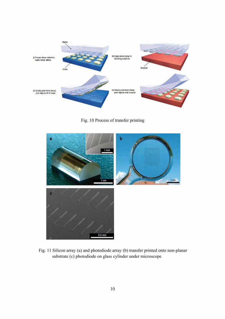
Fig. 10 Process of transfer printing
Fig. 11 Silicon array (a) and photodiode array (b) transfer printed onto non-planar
substrate (c) photodiode on glass cylinder under microscope
10

Chapter 2
Exploration of high fidelity transfer printing based on solution-involved adhesive
strength modulation
2.1 Introduction
Yield is most focused to evaluate the performance of transfer printing
process, some high yield (>99%) transfer printing has been reported with regard to
kinetic approaches that use viscoelasitic stamps for retrieval and delivery. The ability
to switch from strong to weak adhesion is critical to achieve high yield. Shear-offset
has been tried to be applied during delamination to increase yield [17], or change
different preload on the stamp while retract it quickly and slowly to complete the
transfer printing [18], the process is illustrated in Figure 12, different amount of
preload is applied on initial contact with the target substrates. It is reported that
enhancement of yield is facilitated by etching-assisted transfer printing (ETP) for
construction of flexible organic nanowires devices [19]. The PMMA/electrodes films
can be released in the solution to etch away the sacrificial metal layer and combined
with target substrate when the substrate was lifted up in the deionized water bath. In
this chapter, a high fidelity tape transfer printing (TTP) process based on
solution-involved adhesive strength modulation will be proposed, and an array of
target devices and materials before and after transfer printing will be demonstrated.
11

High fidelity (>99%) is realized on the target flexible substrate with retention of
devices’ function. It is helpful to the fabrication of sensors, display devices and other
heterogenerous devices in the future.
Fig. 12 Improve the yield of transfer printing by changing amount of pre-load
2.2 Tape transfer printing
Tape transfer printing has ever been used in fabricating liquid-alloy-based
microfluidic stretchable electronics integrated with wireless communication capability
[20]. The liquid alloy antenna was transfer printed by adhesive tape and hybrid
integrated with ultra-high frequency (UHF) RFID chip to form frequency
identification tag (RFID). Also, tape transfer printing technology has been used to
fabricate flexible nanowires electronics. A thermal release tape serves as supporter of
the devices and attached onto the top of the flexible target substrate.
12

After removal of silicon substrate with assistance of water, the thermal release tape is
heated at 90℃for 5-6s and peeled off, only nanowire device is left on the target
substrate.
Here a novel tape transfer printing process is proposed, details are shown in
Figure 13.
Fig. 13 Tape transfer printing process
13
b
1cm 5mm
AcetonetapePI1cm 1cm
1cm
1cm
c d
e f g
h
200um
i
200um 200um
j
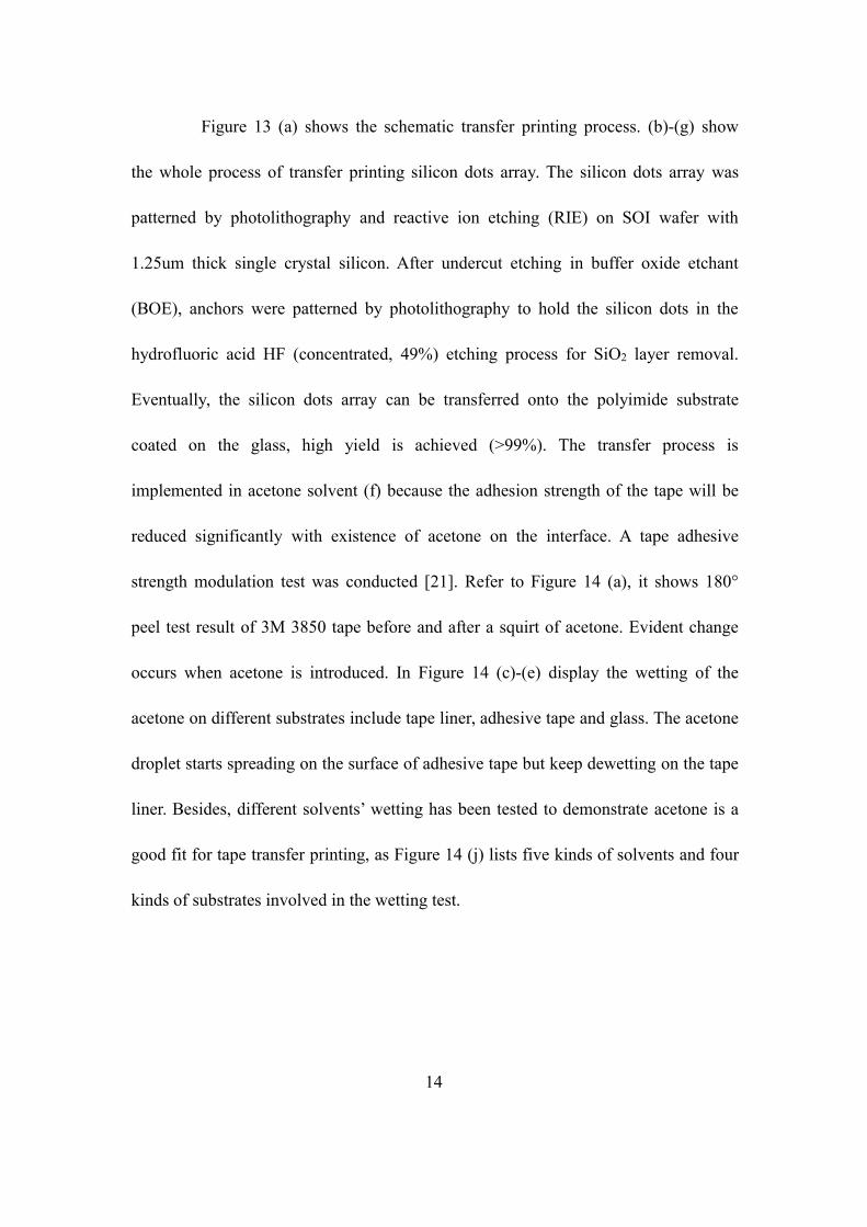
Figure 13 (a) shows the schematic transfer printing process. (b)-(g) show
the whole process of transfer printing silicon dots array. The silicon dots array was
patterned by photolithography and reactive ion etching (RIE) on SOI wafer with
1.25um thick single crystal silicon. After undercut etching in buffer oxide etchant
(BOE), anchors were patterned by photolithography to hold the silicon dots in the
hydrofluoric acid HF (concentrated, 49%) etching process for SiO2 layer removal.
Eventually, the silicon dots array can be transferred onto the polyimide substrate
coated on the glass, high yield is achieved (>99%). The transfer process is
implemented in acetone solvent (f) because the adhesion strength of the tape will be
reduced significantly with existence of acetone on the interface. A tape adhesive
strength modulation test was conducted [21]. Refer to Figure 14 (a), it shows 180°
peel test result of 3M 3850 tape before and after a squirt of acetone. Evident change
occurs when acetone is introduced. In Figure 14 (c)-(e) display the wetting of the
acetone on different substrates include tape liner, adhesive tape and glass. The acetone
droplet starts spreading on the surface of adhesive tape but keep dewetting on the tape
liner. Besides, different solvents’ wetting has been tested to demonstrate acetone is a
good fit for tape transfer printing, as Figure 14 (j) lists five kinds of solvents and four
kinds of substrates involved in the wetting test.
14
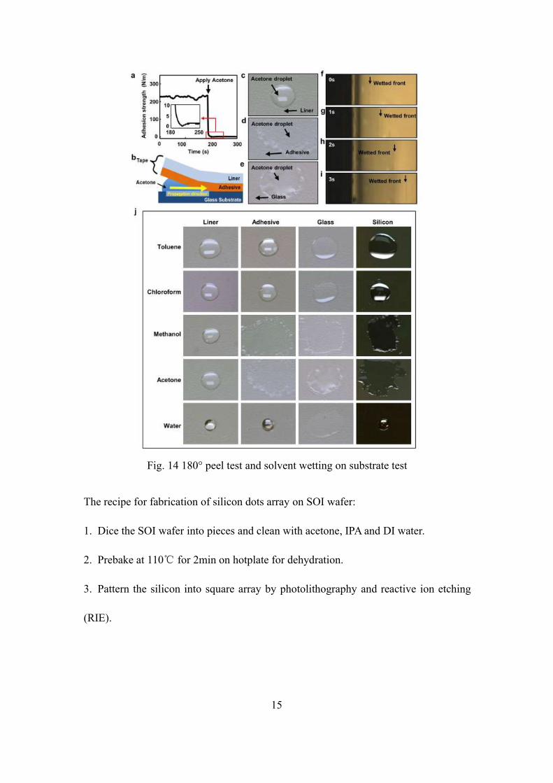
Fig. 14 180° peel test and solvent wetting on substrate test
The recipe for fabrication of silicon dots array on SOI wafer:
1. Dice the SOI wafer into pieces and clean with acetone, IPA and DI water.
2. Prebake at 110℃ for 2min on hotplate for dehydration.
3. Pattern the silicon into square array by photolithography and reactive ion etching
(RIE).
15

4. Immerse the sample into buffer oxide etchant (BOE 1:6) for undercut etching for
15min.
5. Pattern photoresist anchors by photolithography.
6. Immerse the sample into concentrate hydraufluoric acid (HF 49%) for 2hours to
remove the SiO2.
As pointed out, a series of devices can be transfer printed onto flexible
substrate to fulfill target functions. Similar to transfer printing of silicon dots array,
photodetectors array on polyimide substrate is achievable in the same manner. Figure
15 (a) and (b) show the photodiode array before and after transfer printing. (c) is the
microscope blowup of photodiodes on the polyimide film. (d) plots the
current-voltage trends of photodiode under illumination and dark environment. The
device is proved to be working in the target substrate after transfer printing process.
The recipe for fabrication of photodiode:
1-2. Same as the steps in recipe for fabrication of silicon dots array.
3. Spin coat spin-on-glass (700B Filmtronics) on the wafer and pattern by
photolithography and etching to form the doping mask.
4. Phosphorous based spin-on-dopant (P510) was used for doping process at 950℃ to
form the diode.
5. Pattern the silicon into square dots array by reactive ion etching (RIE) using sulfur
hexafluoride (SF6) gas.
16

6-8. Similar to the steps 4-6 in recipe for fabrication of silicon dots array.
Fig. 15 Tape transfer printing of photodiode array onto Polyimide film
Transfer printing technology is applicable to fabrication of epidermis
electronics as it has been reported in the past decade [22, 23, 24]. But tape transfer
printing has never been related to any fabrication of e-sensors for physiological
monitoring. A kind of skin mountable EMG sensors has been realized based on tape
transfer printing and it can work to record EMG signal when being attached on the
arm. The sensor was composed of serpentine electrodes and strip pads, which was
patterned by photolithography on polyimide-coated glass. The sensor can be transfer
printed onto ultralet ozone (O3) treated Ecoflex patch by tape with assistance of
acetone, Figure 16 has shown the flexible EMG sensor and testing. The EMG data
acquisition setup was from biomedical engineering department in UH and the testing
17

program was home-built by MATLAB.
Fig. 16 Transfer printing of EMG sensor onto EcoFLEX patch
The recipe for fabrication of EMG sensor:
1. Clean glass slide with acetone, IPA and DI water, bake it on the hotplate at 110℃
for dehydration.
2. Spin coat polyimide and cure it at 250℃ for one hour.
3. Deposit Ag layer 300nm on the PI by e-beam evaporation.
4. Pattern the electrodes by photolithography.
5. Pattern the PI by RIE under oxygen plasma.
6. Pick up the EMG sensor by using tape 3M3850.
7. Deposit silicon dioxide layer 50 nm on the tape by e-beam evaporation.
8. Spin-coat Ecoflex on the glass and cure at 90℃ for 5 minutes.
9. UV ozone treat the Ecoflex film.
18
Ag/PI

10. Laminate the tape onto the Ecoflex film, heated at 70℃ for 10min to form the
bonding between the SiO2 and the Ecoflex substrate.
11. Prepare acetone in the beaker and immerse the sample in it. Delaminate the tape
and leave the electrodes sensor on the Ecoflex film.
12. Bond the ACF ribbon cables between EMG sensor and PCB interface at 170℃ on
flat iron for 1min.
13. Peel off the film from glass substrate and connect to the data logger the for
testing.
To verify the feasibility of tape transfer printing on other shape substrate,
glass tube and glass rod raft were tried as target substrate due to their curvilinear
surfaces. Before transfer printing, the tube and glass rod raft was coated with PDMS,
Figure 17 shows the silicon dots array printed onto the curvilinear tube and glass rod
raft. The diameter of the tube and rod is about 15mm and 5mm respectively.
Fig. 17 Transfer printing of silicon dot array onto curvilinear shape tube
19
1cm 5mm
a b

Chapter 3
Exploration of fabrication by balloon transfer printing (BTP)
3.1 Introduction
Balloon transfer printing is a novel methodology of fabricating or
assembling semiconductor devices onto dome-shape substrate. Generally, the
fabrication of dome-shape sensors were started from either transfer print the devices
or assemble the devices onto planar substrate, and shape the substrate into curvilinear
dome. Google has rolled out a product named smart contact lens that can help
monitoring the wearer’s glucose level in tear [26]. The fabrication is originated from
heat molding technology developed by University of Washington [27], place and
press a planar lens with components into a heated aluminum mold to form a
curvilinear shape. In this chapter, balloon transfer printing process will be introduced,
transfer printing of metal electrodes and silicon square dots array will be
demonstrated to verify the possibility of high fidelity. Fabrication of smart contact
lens based on balloon transfer printing will be explored, albeit the no functional
device is included. And a novel fabrication of hemispherical helix antenna is proposed
based on BTP process.
3.2 Smart Contact Lens
Smart contact lenses is coming under the spotlight because of its integrated
multi-function features like physiological monitoring and video or image display.
20
Some companies has already rolled out the commercial product onto the market,
specifically Google is taking the lead now and pursuing on making a ‘Google glass’
like smart contact lens that can realize augmented reality in addition to monitoring the
glucose level in tear and the intraocular pressure [27-35]. Also, Samsung has patented
smart contact lens that can create augmented reality experience for user [36].
Meanwhile, another consumer electronics giant SONY launched smart contact lenses
to capture video and image by blinking eyes [37]. Although numerous categories of
smart contact lenses has been created, it is expected that customers will be staggered
continuously by more fancy function in the future.
The earliest one of the applications of smart contact lens is used to monitor
the glucose level in human body. Today, diabetes is widely considered to be the most
deadly disease around the world, and the number of people diagnosed with diabetes
mellitus is estimated to increase dramatically in the next few decades, therefore
continuous monitoring of glucose can help with diagnosis and prevention of the
disease. However, the conventional enzyme-based finger-pricking method used in
diabetic assessment is invasive and may cause patient potential infection in the blood
sampling process. An alternative method which uses near-infrared spectroscopy opens
a door to provide a noninvasive way to infer metabolic concentration by means of
analyzing the light reflection or transmission spectrum in the fingertip. Due to the
poor signal strength and calibration issues, this method is inappropriate for clinical
21

use. Therefore, some research institutions and companies are focusing on the sensible
development of noninvasive and continuous glucose sensor.
The noninvasive monitoring solution of glucose level proposed by Google
is based on electrochemical measurement. The basic electrochemical reaction in
sensing glucose is catalyzing glucose to hydrogen peroxide H2O2 using the enzyme
glucose oxidase (GOD) [38, 39]. H2O2 is further oxidized at the electrode to release
electrons, generating a current signal proportional to the glucose concentration in the
tear. To fabricate a stable electrochemical sensor, three electrodes are typically used: a
working electrode (WE) a counter electrode (CE) and a reference electrode (RE).
Those comprise the typical electrochemical measurement configuration. Particularly,
the working and counter electrodes are designed as concentric rings to decrease the
resistance and thus enhance the sensor sensitivity.
The design of the contact lens for glucose monitoring features its circuit
implementation, which initially come out of the research in University of Washington.
The signal of the on-lens sensor is read out by wireless IC which consists of a power
management block, readout circuitry, wireless communication interface, LED driver,
and energy storage capacitors in a 0.36mm2 CMOS chip [39, 40]. The system is
wirelessly powered by RF feed from an interrogator, and the energy is converted into
stable 1.2-V by rectifier and regulator circuit. The data is transmitted by backscatter
communication manner to interrogator to be decoded by the reader. In Google’s new
22

commercial smart contact lens, a compact ASIC chip is used instead of home-built
wireless IC to realize the data transmission function.
Besides the application in monitoring the glucose level in tear fluid, other
different functions that can make the contact lens smarter has been implemented, such
as RF-powered lens with single element display [41]. The micro-LED were grown on
an aluminum gallium arsenide, powered by a CMOS chip includes energy harvester,
power management unit and energy storage unit. This is a one step forward to realize
display of all kinds of text and image in augmented reality style. Afterwards, the
researchers have integrated blue micro-LED arrays and micro-Fresnel lenses on the
contact lens to create a multi-pixels effect on retina, like letters or numbers or
combination of both [42]. It is expected that more than just simple notifications can be
given on the lens to have effect of augmented reality. The prototype lens was tried on
rabbit’s eye and was proven to have a good biocompatibility.
Generally, the power to support smart contact lenses comes from wireless
energy transmission. The RF power is fed into the system through antenna from
nearby source, but the drawback of this method is the low efficiency of small antenna
embedded around the edge of the contact lens and a handheld device is required to
send RF wave. To upgrade the energy feed, photovoltaic device like solar cell has
been integrated on the contact lens so that it can absorb energy from ambient light and
convert it into several microwatts eletrical power, even in-doors [43]. The solar cell
23

can provide enough energy to make the other devices or chip on lens work. The solar
cells were assembled in array and has 14.3% efficiency at AM2.0, it is a little lower
than the crystalline solar cell of the near size. But some problems lie in that whether
the solar cell can work on the night as well as whether the solar cell would block the
vision of the wearer. The feasibility will be unveiled in the future.
Apart from Google, another company focuses on the smart contact lens is
the Sensimed Co. The Switzerland located spinoff mainly fabricates patented
Triggerfish@ digital active smart contact lens that can continuously monitor wearer’s
intraocular pressure (IOP) to diagnosis glaucoma, chronic and progressive disease due
to the damage of optic nerve that will cause the patient irreversible blindness
eventually. The conventional ways to detect the glaucoma is through visual acuity and
visual field testing [44], optic nerve examination and tonometry [45], however, those
ways are limited and inconvenient because the peak of intraocular pressure occurs on
the morning or night, nocturnal measurement of IOP is generally inaccessible.
Triggerfish@ can provide 24-hour monitoring of IOP without any interference of
wearer’s life and sleep, so this helps the doctor identify the best time to measure
patient’s IOP. So far, the Triggerfish@ has been approved by European regulatory
authorities (Class IIa device CE-mark) and available on the market. And FDA has
approved the marketing in early 2016.
The key element in Triggerfish@ smart contact lens is a microfabricated
24

strain gauge that can measure the change in the cornea curvature proportional to the
IOP. This technology or method dates back to 1967, when Gillman and Greece
presented an embedded strain gauge in contact lens to measure the angular change of
corneoscleral junction because of the IOP fluctuation [46]. The drawback of the
invention is that the curvature of contact lens has to be the same of that of wearer’s
eyes. This will make the contact lens expensive and eventually ended up with
abandon. Different from strain gauge, the strain gauge used in Triggerfish@ is
configured like Wheatstone bridge: two arms act as sensing resistive gauges, and the
other two arms act as thermal compensation resistive gauges and placed radically. A
dedicated ASIC is used for wireless data transmission at 27MHz, which is a about
50um thick and attached on the lens by common flip-chip technology. This ASIC is
connected to a small antenna loop and the active sensor. Energy is fed in from a pair
of glasses and a patch for overnight measurement, the data is transmitted onto a
portable unit around wearer’s waist and sent to PC by Bluetooth.
As a commercial product, Triggerfish@ is proven to have high comfort score
during the 24 hour clinical study, a study run on 15 patient attests to the safety and
comfort. Despite contact lens malfunction happened on one patient, no other adverse
effect was observed. It was reported that non-IOP-related change such as cornea
swelling due to the insufficient reach of oxygen through closed eyelid during the
wearer’s sleep has minimal effect to the data output, hence, the Triggerfish@ smart
25

contact lens is considered to be a fitting device that can be integrated into the clinical
practice and so far it’s taking the lead in IOP continuous monitoring device market.
As for smart contact lens for IOP monitoring, researcher H. Cong and T.
Pan in UC Davis has developed a contact lens that can real-time measure the IOP [47].
Differ from the resistive pressure gauge embedded in Triggerfish@, such pressure
sensor is capacitive sensing features a unique photosensitive composite, which
comprises PDMS polymer, silver powder and photosensitive reagent. Pattern a wafer
with such composite of photoresist by photolithography and then bond it with flexible
substrate, the device is able to be shaped into contact lens by thermal compression.
The fabrication is as same as the one used for smart contact lens created by University
of Washington, while the planar substrate with devices was pressed in aluminum
mold with high temperature, 180℃ to cast a contact lens with desired curvature [48].
However, one of the drawbacks of such a fabrication is the low yield. The devices
may easily break in the process of thermal compression; Besides, it is inconvenient to
polish the lens edge after molding. Because of this, a better solution is required. A
new transfer printing process called balloon transfer printing (BTP) proposed here
serves the needs of picking up the devices and transferring to the target contact lens
and will reduce the risk of damaging the devices a high yield is expected. Compared
to the thermal compression, such technology provides a more sensible option due to
convenience and simple operation and will be potentially deployed in fabrication of
26

smart contact lens in the future. More details about BTP will be covered in the next
part.
3.3 Balloon Transfer Printing
The principle of balloon transfer printing process is same to other transfer
printing process. Polymer-coated balloon serves as stamp that can be used to pick up
the device on the donor and transferred to the receiver. The whole process is
illustrated in Figure 18 (a).
Fig. 8
Fig. 18
Fig. 18 Balloon transfer printing (BTP) process
250umx250mm silicon square dots array was fabricated following the same recipe as
mentioned in last chapter. The balloon was coated by PDMS and left still for 24 hours
to dry, then pressed the balloon onto the sample wafer to pick up the dots array,
27
a
b c d
5 mm
250 um
1 cm2mm
PDMS
Ecoflex

almost all the silicon pellets can be attached on the PDMS film (Fig. 18 (b)-(c)). The
Ecoflex dome was placed on the cylinder stand with hemispherical head after 5-min
exposure to UV ozone to strength the bonding. Eventually contacted the balloon onto
the dome being heated at 70℃ and retrieved, high fidelity is realized (>99%, Fig. 18
(d)) after the process. One problem in the process is misalignment occurred during the
manual operation, but this can be fixed later when PC controlled platform is
introduced.
For flexible electronics, all the sensors, chips and electronics components
are connected by serpentine interconnects. To verify the metal mesh can be transfer
printed by polymer-coated balloon, a copper metal mesh network sandwitched
between polyimide film is tested for trial. Fig. 19 (a) and (c) show the 3-layer metal
mesh ring, the target dome was moulded and placed on the top of a steel cylinder
stand for transfer printing. The final look of the dome with mesh pattern is shown in
(b). To verify the feasibility of smart contact lens, some pseudo devices resemble
sensors, LED array and contact pads with no function were fabricated in the
encapsulation of polyimide films and connected by polyimede serpentine wires to
comprise a network. (e) shows a demo of such ‘smart contact lens’ while (d) shows
the planar structure before transfer printing. The metal pads were used for connection
of ACF ribbon cable for testing. Due to the fact that the sensors have no practical
function, no further testing was conducted.
28
One of applications of balloon transfer printing in fabricating functional
device is helix antenna. Conventionally, the hemispherical helix or meanderline
antenna is printed onto the conformal substrate like glass by 3D printer [49], directly
transfer printed onto contoured substrate [50], or attached on the planar substrate and
pneumatically inflated into spherical cap [51]. Similar to the fabrication of devices on
hemispherical substrate by BTP, a planar copper antenna is patterned by
photolithography first and transfer printed onto the dome, Figure 19 (f) and (g) show
the antenna before and after printing. The testing of the antenna was conducted in
anechoic chamber, the dome was fixed on the petri dish covered with copper foil and
four signal wires were extended from the pads for electrical connection (Figure 19
(h)). Two samples have been tested and result shows a resonant dip at 3.55GHz and
3.52GHz respectively, which matches the simulation result, resonant dip appears at
3.69GHz (Figure 19 (j)).
29

Fig. 19
Fig. 19 Transfer printing of serpentine metal mesh and antenna
30
f
Sample 1 Sample 2 Simulation
3.52GHz 3.69GHz
3.55GHz
ji
5 mm5 mm
ed
5 mm 400 um
ca PI, Cu, PI
5 mm
b
Cu
5 mm
ground
signal
conductive foil
250 mm5 mm
g hf

Chapter 4
Exploration of eSkin technology
4.1 Wearable electronics
‘Wearable electronics are electronic devices constantly worn by a person as
unobstructively as clothing to provide intelligent assistance that augments memory,
intellect, creativity, communication and physical senses’ [52].
Wearable electronics come under the spotlight in the recent years because they are
sensors or computers attached on the human body features compact, flexible and
functional. Those devices can be worn in the form of badge, bandage, patch,
eyeglasses and wristwatch for the purposes of smart physiological monitoring and
all-the-time human machine interaction. Numerous research institutes and companies
has put a lot of efforts to develop more sensible and advanced wearable electronics
devices. Google has rolled out a pair of glasses that wearer can interact with it to
obtain information from internet through natural language voice. Earlier in 2016,
Google also developed successfully a smart contact lens that combines multiple
functions into the tiny dome. The lens can sense the level of glucose in the tear in eyes
and transmit the real-time data to user-end by RF. The is a huge breakthrough because
the diabetics don’t need to rely on conventional painful finger-pricking measurement,
which requires special device for analysis. And operation at home becomes possible.
Besides Google, Samsung has been working on patented smart contact lens
31

for augment reality by adding a built-in camera. SONY has synchronously unveiled a
contact lens embedded with organic electroluminescence display screen that makes
video watching become true, and wearer can control the video recording operation by
blinking eyes. To prevent mis-orientation, a gyro is included to detect and bring the
video to correct orientation when the user tilts head. Apple doesn’t activate their smart
contact lens plan but has launched two series Apple Watch incorporated with fitness
tracking and health monitoring, seamlessly integrated with iOS. The Apple Watch has
built-in sensors include gyroscope, accelerometer and magnetometer as core motion
which can track all the wearer’s activities, e.g. How much time wearer’s spent doing
brisk activity and how many calories wearer’s burned. And strikingly, ample apps are
off the shelf in addition to the activity app on the watch itself, wearer can monitor
heart rate if select a health app on the iPhone.
Fig. 20 Google Co.’s Smart Contact Lens for glucose monitoring
4.2 Skin mountable electronics
Courtesy of advances of flexible electronics, a constellation of sensors and
32

devices become possible to be printed onto the wearer’s skin. The so-called ‘epidemic
electronics’ or ‘smart bandage’ is composed of elastomeric patch, sensors, devices,
electronic components and circuit, which can be attached on the surface of epidermis
to take measurement of electrophysiological (EP) signal from nerve and muscle
activity or other skin properties like temperature, hydration and strain. Usually to
acquire EP signal, the electrodes should be laid out in form of serpentine meshes and
integrated with skin in conformal manner by Van der Waals interaction. To increase
the robustness of measurement, capacitive sensing is employed to encapsulate
electrodes between layers of polymer. Figure 21 shows a 3-electrode structure of
capacitive sensor and Figure 22 shows comparison of electrocardiograms (ECGs)
signal measured by using conventional gel electrodes direct contact (Blue), direct
contact electrode (Red), and capacitive epidermis electronics (Green). The conductor
is made of metal Au while Solaris is chosen as insulating layer due to its attractive
features like large stretchability, adhesion force, strong signal coupling and robust
skin lamination. The same capacitive epidermis sensor can also work on
electromyograms (EMG) and electrooculograms (EOG) measurement. The EMG
signal was recorded on the flexor carpi radialis of the forearm at different motions of
hand like in Figure 22 and Figure 23. The EOG signal is measured near left and right
eyes when reading a book (Figure 22 (e)). Such epidermis electronics features good
wearability and minimum leaking currents, research on combination with wireless
33

data transmission for telemedicine is being widely conducted.
Fig. 21 Capacitive epidermic sensor
Fig. 22 Electrocardiograms (ECGs) signal and measurement on chest, forearm and
near left and right eye
34
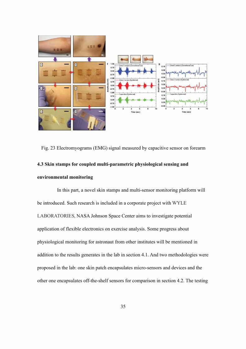
Fig. 23 Electromyograms (EMG) signal measured by capacitive sensor on forearm
4.3 Skin stamps for coupled multi-parametric physiological sensing and
environmental monitoring
In this part, a novel skin stamps and multi-sensor monitoring platform will
be introduced. Such research is included in a corporate project with WYLE
LABORATORIES, NASA Johnson Space Center aims to investigate potential
application of flexible electronics on exercise analysis. Some progress about
physiological monitoring for astronaut from other institutes will be mentioned in
addition to the results generates in the lab in section 4.1. And two methodologies were
proposed in the lab: one skin patch encapsulates micro-sensors and devices and the
other one encapsulates off-the-shelf sensors for comparison in section 4.2. The testing
35

for skin patch encapsulates commercial devices will be introduced in section 4.3, an
open sourced Arduino Uno platform will be used to log the data acquired from the
devices and display the data real-time on GUI by script Section 4.4 demonstrates the
experiment results.
4.3.1 Physiological monitoring application for astronauts
To guarantee the safety of astronaut during space flight and extravehicular
activities, the physiological condition of the astronaut should be monitored and
analyzed real-time. However, unlike people in earth environment, astronaut’s body is
encapsulated in garment assembly where conventional apparatus and electrical
connection is hard to access. To this end, a lot of projects are being sponsored to
investigate the applications of biosensors attached on the body that can record the
health and psychological data and pass to logging device for processing. NASA and
Stanford University aim to develop a system that integrates biosensors and a wearable
processing unit called Crew Physiologic Observation Device (CPOD), whose
real-time transmission of data to base unit is enabled by Bluetooth wireless
technology. Such LifeGuard system is radiation repellent, can survive extreme-rugged
environment and integrated function of measurement of blood oxygen saturation,
ECG, respiration rate, temperature, heart rate pulse oximetry (SpO2), diastolic and
systolic blood pressure. Figure24 shows arrangement of sensors and CPOD straped on
the body and details about CPOD.
36

Fig. 24 Crew Physiologic Observation Device (CPOD)
Besides, a Space Sock System composed of heterogenerous sensor network,
processor module VPack and spacesuit CAIPack computer was developed by a
research group in Virginia Commonwealth University [53], and performance
evaluation test was conducted with the supervision of NASA’s Extra-Vehicle
Activities (EVA) division based in Johnson Space Center. The biomedical sensor
signals were acquired by Space Sock that contains plethysmograph sensor, Galvin
skin resistance sensor,skin temperature sensor,and a pulse oximetry sensor. The
CAIPack in the platform servers as hub for data collection and data presentation on
helmet mounted display, and data packets can be routed to remote station in Mission
Control Center in Houston. Further development aims to integrate sensors for more
physiological monitoring like respiration rate sensor and body accelerator.
Differ from the monitoring sensor network proposed for astronaut’s
physiological monitoring, a new skin mountable stamps that include various kinds of
37

sensors in a patch has been developed in Wearable Electronics Group in UH, such
stamp can acquire several physiological signals on part of body and send to the
processing unit either by wired or wireless communication. More details will be
covered in the next part.
4.3.2 Ultra-thin skin mountable stamps
The research on stretchable micro-sensors has been introduced in the
previous chapter. It has been demonstrated that the sensors can be transfer printed
onto the skin as e-tatoo. Another approach to make a skin stamp is to encapsulate the
sensors in elastomer or flexible patch as shown in Figure 25, all the sensors
(temerature, UV, strain and ion) are connected in serpentine meshes network. Figure
26 (a) and (b) show the mask design of each seperate sensor, (c) is the blowup that
shows the detailed structure. The gold metal layers were sandwitched between
polyimide (PI) layers and strikingly, the 6-layer IZO was deposited on the polyimide
as transparent electrodes. All the fabrication was carried out in cleanroom in UH and
the recipe of fabricating IZO devices is list below:
1. Etch marker (Cu, E-beam & photolithography)
2. Coat Polyimide
3. Coat IZO
4. Pattern IZO (photolithography, wet etching)
5. Deposit 1st metal layer (Au, photolithography & E-beam; lift off)
38

6. Form gate dielectric (SU-8)
7. Deposit 2nd metal layer (Au, photolithography & E-beam; lift off)
8. Coat Polyimide
9. Pattern PI (photolithography, RIE etching)
Fig. 25 IZO devices for physiological monitoring
39

Fig. 26 Mask design of IZO devices
40
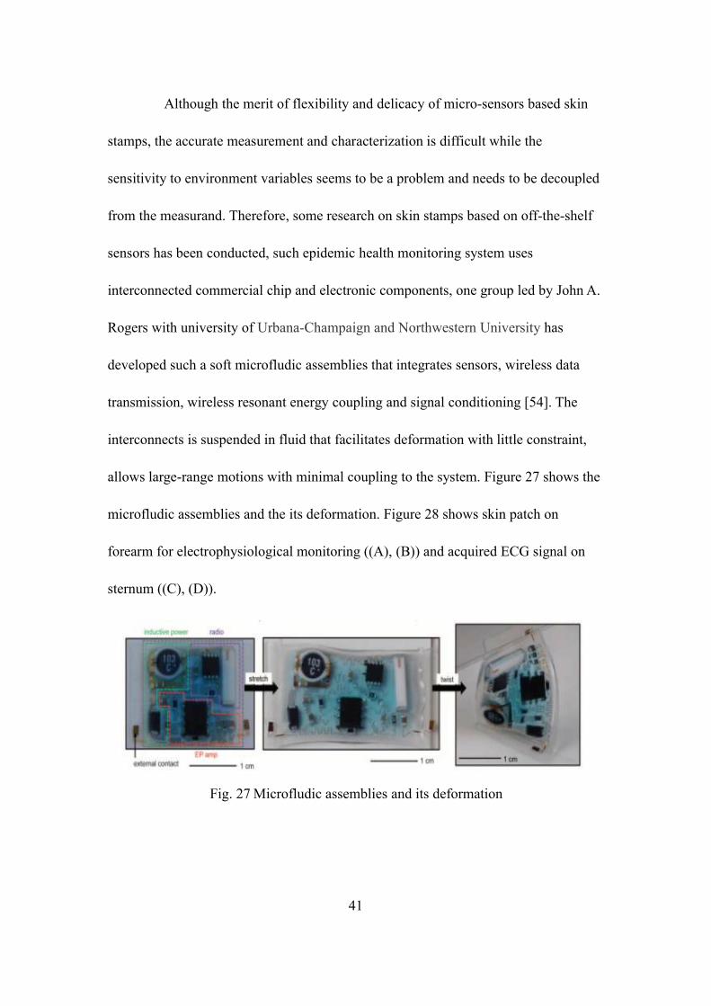
Although the merit of flexibility and delicacy of micro-sensors based skin
stamps, the accurate measurement and characterization is difficult while the
sensitivity to environment variables seems to be a problem and needs to be decoupled
from the measurand. Therefore, some research on skin stamps based on off-the-shelf
sensors has been conducted, such epidemic health monitoring system uses
interconnected commercial chip and electronic components, one group led by John A.
Rogers with university of Urbana-Champaign and Northwestern University has
developed such a soft microfludic assemblies that integrates sensors, wireless data
transmission, wireless resonant energy coupling and signal conditioning [54]. The
interconnects is suspended in fluid that facilitates deformation with little constraint,
allows large-range motions with minimal coupling to the system. Figure 27 shows the
microfludic assemblies and the its deformation. Figure 28 shows skin patch on
forearm for electrophysiological monitoring ((A), (B)) and acquired ECG signal on
sternum ((C), (D)).
Fig. 27 Microfludic assemblies and its deformation
41
Fig. 28 Skin patch on forearm for electrophysiological monitoring
For the purposes of monitoring multiple physiological parameters of
astronaut or athlete, more sensors should be involved besides common temperature,
ECG and strain sensors. To this end, one kind of skin patch has been fabricated
coupled temperature sensor, skin hydration sensor, pulse rate sensor and gas
concentration sensor for exercise analysis. Compared to other skin patch, this skin
42

patch uses wires transmission in place of wireless data transmission, all the
measurand is sent to Arduino Uno development board and displayed on GUI by
running a MATLAB script. The schematic of the skin mountable patch is shown in
Figure 29.
Fig. 29 Skin mountable patch
4.3.2.1 Arduino Uno
Arduino Uno is an open source microcontroller board based on 8-bit AVR
RISC-based microcontrollor ATmega328P. It has 14 digital IO ports and 6 analog
input ports. The board can be powered either by AC-DC adaptor or USB connection
directly. Program in Arduino IDE and download the sketch into the memory can make
the board start to work. The whole operation is straight-forward and easy to handle, so
it becomes so popular among the electronics geeks and engineers.
43
Gas concentration
sensor
Temperature sensor
Skin hydration sensor
Pulse rate sensor

4.3.2.2 Sensors
1. Thermistor MCP9700
The MCP9700/9700A and MCP9701/9701A family of Linear Active
Thermistor Integrated Circuit (IC) is an analog temperature sensor that converts
temperature to analog voltage. It is a low-cost, low-power sensor with an accuracy of
±2℃ from 0℃ to +70℃ (MCP9700A/MCP9701A) while consuming 6μA operating
current. Strikingly, no signal conditioning circuit is required, the voltage output pin
can be directly connected to the ADC input of microcontroller. The temperature
coefficients are scaled to provide a 1℃/bit resolution for an 8-bit ADC with a
reference voltage of 2.5V and 5.0V respectively.
The connection of temperature sensor and Arduino board is shown below, in
44

Figure 30. Three wires include power, ground and signal. The signal wire goes into
the analog 0 port on the board while the power goes into the +5V port.
Fig. 30 Thermistor and connection to Arduino Uno
2. Humidity sensor HIH-4030
The HIH-4030/4031 is covered IC humidity sensor that is factory-fitted
with a hydrophobic filter allowing it to be used in condensing environments including
industrial, medical and commercial application. Direct input to a controller or other
device is made possible by the sensor’s near linear voltage output. With typical
current draw of only 200μA, the HIH-4030/4031 series ideally suited for low drain,
battery operated system.
45

3. Pulse sensor
Pulse sensor ICSG007A is a compact optical pulse sensor that integrates
amplification circuit and noise nullification circuit to make pulse readings precise and
quick. It consumes 4mA current draw at 5V and can be clipped to earlobe or fingertip
for heart rate monitoring when being plugged into the Arduino board.
4. Carbon dioxide sensor
IR1011 from Asahi Kasei Microdevices Corporation feartures world’s
smallest quantum photodiode (2.65mmX1.9mmX0.4mm), it is SMD package that can
be mounted onto PCB of fast response, high sensitivity and no bias current is
46

required.
It is applicable to human body detection, non-contacting temperature measurement
and NDIR gas sensor.
5. Oxygen sensor
No applicable compact oxygen sensor is available after a wide search online,
therefore, no oxygen sensor is involved in the demo.
4.3.2.3 Result
To verify the feasibility of skin mountable patch composed of commercial
components, temperature and humidity sensors from online shop were chosen and
encapsulated into the polymer patch. To this end, EcoFlex rubbers should be prepared
by mixing A and B at ratio 1:1 by weight and poured onto the sensor, let alone for
couples of hours to solidify. The Figure 31 shows the rubber patch with embedded
sensors, and the skin patch attached on the epidermis of arm and data acquisition
hardware Arduino Uno board.
Fig. 31 Skin mountable patch embeds temperature and humidity sensors
47
1cm
HIH-4030
1cm
MCP9700
1cm
MCP9700
Cables Humidity sensor
Arduino Uno

The data acquired by the skin patch in 5s is illustrated in the Figure 32 and
Figure 33, one is the relative humidity in environment vs on skin surface and the other
one is the temperature in environment vs on skin surface. An evident difference can be
found on the on the picture.
Fig. 32 Humidity in environment and on skin surface
48

Fig. 33 Temperature in environment and on skin surface
To monitor more physiological signals from astronaut or sportman, more
off-the-shelf sensors can be embedded into the Ecoflex patch. Figure 34 shows a skin
mountable patch includes pulse sensor and gas sensor besides temperature sensor and
humidity sensor. For the purposes of real-time displaying the trend of the acquired
signal, a simple script was built by MATLAB, Figure 35 shows the curves of readout.
On the right is the data acquisition device and 2-m ribbon cable used for connection to
Arduino Uno board. To realize wireless transmission, a transmit-receive module
should be deployed and more research can be conducted in the future.
49

Fig. 34 Skin mountable patch and Arduino Uno
Fig. 35 Real-time acquisition and display of data from sensors
50
Pulse rate (BPM)
Relative humidity (%)
Temperature (Celsius)
Temperature
sensor
Humidty sensor
Gas sensor
Ribbon cable
Pulse sensor

MATLAB script:
a = arduino('COM5');
interv = 1000;
passo = 1;
t=1;
x=0;
y=0;
z=0;
while(t<interv)
b=readVoltage(a,'A0');
temp=(b-0.5)/0.01;
x=[x,temp];
fid=fopen('Temperature.txt','w');
fprintf(fid,'Temperature data\n\n');
fprintf(fid,'%f\n',x);
fclose(fid);
c=readVoltage(a,'A1');
RH=161*c/5-25.8;
U=RH/0.9896;
y=[y,U];
51

fid=fopen('Humidity.txt','w');
fprintf(fid,'Humidity data\n\n');
fprintf(fid,'%f\n',y);
fclose(fid);
d=readVoltage(a,'A2');
U=d*23;
z=[z,U];
fid=fopen('Pulserate.txt','w');
fprintf(fid,'Pulserate\n\n');
fprintf(fid,'%f\n',z);
fclose(fid);
plot(x);
legend();
grid
t=t+passo;
drawnow;
hold on
plot(y);
drawnow;
hold on
52

plot(z);
drawnow;
legend('Pulse rate','Humidity','Temperature');
title('Sensor readout');
end
53

Chapter 5
Conclusion
Introduction to transfer printing especially two novel methods for realization with
assistance of tape and coated balloon has been made in this thesis. Experiments on
transfer printing of functional devices onto the substrates to form a sensible
electronics has been done, especially tentative combination of balloon transfer
printing and fabrication of smart contact lens blazes the trail. More research on the
balloon transfer is anticipated, heterogenerous integration of multiple devices to
consummate smart contact lens will be a good direction although technical hiccups
including silicon cracks are subject to effective solution. Besides, research on skin
mountable patch for physiological monitoring has been being conducted, in this work,
off-the-shelf components and sensors have been tried out to verify the feasibility in
real-time application, however, the volume of the devices hinder the attachment onto
the skin, therefore more work on design of precise, tiny and applicable flexible
devices with convenient communication interface will be conducted in the future.
54

References
1. Y. N. Xia, J. Tien, D. Qin and G. M. Whitesides, Non-photolithographic methods
for fabrication of elastomeric stamps for use in microcontact printing, Langmuir, 12,
(1996).
2. J .A. Rogers, J. Tate, W. Li, Z. Bao and A. Dodabalapur, Printed organic transistors
and molded plastic lasers, Israel Journal of Chemistry, 39, (1999).
3. J. A. Rogers, Z. Bao, M. Meier, A. Dodobalapur, O. J. A. Schueller, G. M.
Whitesides, Printing, molding, and near-field photolithographic methods for
patterning organic lasers, smart pixels and simple circuits, Synthetic Metals, 115
(2000).
4. A. Kumar and G. M. Whiteside, Features of gold having micrometer to centimeter
dimensions can be formed through a combination of stamping with an elastomeric
stamp and an alkanethiol "ink" followed by chemical etching, Appl. Phys. Lett., 63
(14), (2002).
5. J. L. Wilbur, E. Kim, Y. Xia, G. M. Whitesides, Lithographic molding: A
convenient route to structures with sub-micrometer dimensions, Adv. Mater. 7 (7),
(1995).
6. A. Bernald, J. P. Renault, B. Michel and E. Delamarche, Microcontact Printing of
Proteins, Adv. Mater., 12 (14), (2000).
7. Y.-L. Loo, D. V. Lang, J. A. Rogers, and J. W. P. Hsu, Electrical Contacts to
55
Molecular Layers by Nanotransfer Printing, Nano Letters, 3 (7), (2003).
8. Y.-L. Loo, R. L. Willett, K. W. Baldwin and J. A. Rogers, Additive, nanoscale
patterning of metal films with a stamp and a surface chemistry mediated transfer
process: Applications in plastic electronics, Appl. Phys. Lett., 81 (3), (2002).
9. Y. Sun and J. A. Rogers, Printed arrays of aligned GaAs wires for flexible
transistors, diodes, and circuits on plastic substrates, Nano. Lett., 4 (10), (2004).
10. H. Shimoda, S. J. Oh, H. Z. Geng, R. J. Walker, X. B. Zhang, L. E. McNeil and O.
Zhou, Self-assembly of carbon nanotubes, Adv. Mater., 14 (12), (2002).
11. J. C. Lewenstein T. P. Burgin, A. Ribayrol, L. A. Nagahara and R. K. Tsui,
High-yield selective placement of carbon nanotubes on pre-patterned electrodes, Nano
Lett., 2 (5), (2002).
12. M. A. Meitl, Y. Zhou, A. Gaur, S. Jeon, M. L. Usrey, M. S. Strano and J. A.
Rogers, Solution Casting and Transfer Printing Single-Walled Carbon Nanotube Films,
Nano Lett. 4 (9), (2004).
13. S.-H. Hur, O. O. Park, and J. A. Rogers, Extreme bendability of single-walled
carbon nanotube networks transferred from high-temperature growth substrates to
plastic and their use in thin-film transistors, Appl. Phys. Lett., 86, (2005).
14. S.-H. Hur, C. Kocabas, A. Gaur, O. O. Park, M. Shim and J. A. Rogers, Printed
thin-film transistors and complementary logic gates that use polymer-coated
single-walled carbon nanotube networks, J. Appl. Phys., 98, (2005).
56

15. H. Ahn, K. J. Lee, A. Shim, J. A. Rogers and R. G. Nuzzo, Additive
Soft-Lithographic Patterning of Submicrometer- and Nanometer-Scale Large-Area
Resists on Electronic Materials, Nano Lett., 5 (12), (2005).
16. M. A. Meitl, Z. -T. Zhu, V. Kumar, K. J. Lee, X. Feng, Y. Y. Huang, I. Adesida, R.
G. Nuzzo and J. A. Rogers, Transfer printing by kinetic control of adhesion to an
elastomeric stamp, Nature Materials, 5, (2006).
17. E. Menard, Printing semiconductor elements by shear-assisted elastomeric stamp
transfer,US 8506867.
18. S. Kim, J. Wu, A. Carlson, S. H. Jin, A. Kovalsky, P. Glass, Z. J. Liu, N. Ahmed, S.
L. Elgan, W. Q. Chen, P. M. Ferreira, M. Sitti, Y. G. Huang and J. A. Rogers,
Microstructured elastomeric surfaces with reversible adhesion and examples of their
use in deterministic assembly by transfer printing, PNAS, 107 (40), (2010).
19. W. Deng, X. J. Zhang, H. H. Pan, Q. X. Shang, J. C. Wang, X. H. Zhang, X. W.
Zhang and J. S. Jie, A High-yield two-step transfer printing method for large-scale
fabrication of organic single-crystal devices on arbitrary substrates, Scientific Reports,
4, (2014).
20. S. H. Jeong, K. Hjort, Z. G. Wu, Tape transfer printing of a liquid metal alloy for
stretchable RF electronics, Sensors, 14 (9), (2014).
21. Kyoseung Sim, Song Chen, Yuhang Li, M. Kammoun, Y. Peng, M. W. Xu, Y. Gao,
J. Z. Song, Y. C. Zhang, H. Ardebili and C. J. Yu, High fidelity tape transfer printing
57

based on chemically induced adhesive strength modulation, Scientific Reports, 5,
(2015).
22. D.-H. Kim, N. S. Lu, R. Ma, Y. -S. Kim, R. -H. Kim, S. D. Wang, J. Wu, S. M.
Won, H. Tao, A. Islam, K. J. Yu, T. -I. Kim, R. Chowdhury, M. Ying, L. Z. Xu, M. Li,
H. -J. Chung, H. Y. Keum, M. McCormick, P. Liu, Y. -W. Zhang, F. G. Omenetto, Y. G.
Huang, T. Coleman and J. A. Rogers, Epidermal Electronics, Science, 12, (2011).
23. J. H. Kim, A. Banks, Z. Q. Xie, S. Y. Heo, P. Gutruf, J. W. Lee, S. Xu, K. -I. Jang,
F. Liu, G. Brown, J. H. Choi, J. H. Kim, X. Feng, Y. G. Huang, U. Paik and J. A.
Rogers, Miniaturized Flexible Electronic Systems with Wireless Power and
Near-Field Communication Capabilities, Adv. Func. Mater., 25 (30), (2015).
24. W.-H. Yeo, Y. -S. Kim, J. W. Lee, A. Ameen, L. Shi, M. Li, S. D. Wang, R. Ma, S.
H. Jin, Z. Kang, Y. G. Huang and J. A. Rogers, Multifunctional Epidermal Electronics
Printed Directly Onto the Skin, Adv. Mater., 25, (2013).
25. http://www.newsweek.com/google-patent-cyborg-smart-lens-inject-eyeballs-
455824
26. http://www.sammobile.com/2016/04/05/samsung-is-working-on-smart-
contact-lenses-patent-filing-reveals/
27. N. M. Farandos, A. K. Yetisen, M. J. Monteiro, C. R. Lowe and S. H. Yun,
Contact lens sensors in ocular diagnostics, Adv. Healthcare Mater., 4 (6), (2015).
28. Z. H. Liu, Contact lenses having two-electrode electrochemical sensors,
58

WO2015041716A1, Google Inc., (2015).
29. H. F. Yao, A closed loop control system based on a non-invasive continuous sensor,
WO2015076991A1, Google Inc., (2015).
29. J. Etzkorn, Assembling thin silicon chips on a contact lens, US8960899, Google
Inc., (2015).
30. Z. H. Liu, Microelectrodes in an ophthalmic electrochemical sensor, US8965478,
Google Inc., (2015).
31. J. Etzkorn, B. A. Parviz, Contact lens having an uneven embedded substrate and
method of manufacture, US8985763, Google Inc., (2015).
32. J. Etzkorn, Systems and methods for encapsulating electronics in a mountable
device, US9009958, Google Inc., (2015).
33. B. Otis, Y. -T. Liao, B. A. Parviz, H. F. Yao, Wireless powered contact lens with
glucose sensor, US 20120245444, University of Washington, (2012).
34. J. Pandey, Y. -T. Liao, A. Lingley, R. Mirjalili, B. A. Parviz and B. P. Otis, A fully
integrated RF-powered contact lens with a single element display, IEEE Transactions
on Biomedical Circuits and Systems, 4 (6), (2010).
35. http://mashable.com/2016/04/05/samsung-smart-contact-lenses-patent/#bgZrXUo
EYaqO
36. http://www.pocket-lint.com/news/137527-sony-smart-contact-lens-will-record-ev
erything-you-see-with-the-blink-of-an-eye
59

38. H. Yao, A. J. Shum, M. Cowan, I. Lahdesmaki and B. A. Parviz, A contact lens
with embedded sensor for monitoring tear glucose level, Biosens Bioelectron, 26(7),
(2011).
39. Y.-T. Liao, H. F. Yao, A. Lingley, B. A. Parviz and B. P. Otis, A 3 uW CMOS
Glucose Sensor for Wireless Contact-Lens Tear Glucose Monitoring, IEEE Journal of
solid-state circuits, 47 (1), (2012).
40. Y.-T. Liao, H. F. Yao, B. A. Parviz and B. P. Otis, A 3 uW wirelessly powered
CMOS glucose sensor for an active contact lens, IEEE International solid-state
circuits conference, (2011).
41. A R Lingley, M. Ali, Y. -T. Liao, R. Mirjalili, M. Klonner, M. Sopanen, S.
Suihkonen, T. Shen, B. P. Otis and H. Lipsanen, A single-pixel wireless contact lens
display, J. Micromech./Microengr., 21 (12), (2011).
42. R. Mirjalili and B. A. Parviz, Microlight-emitting diode with integrated Fresnel
zone plate for contact lens embedded display, J. Micro/Nanolith. MEMS MOEMS, 11
(3), (2012).
43. A. R. Lingley, B. P. Otis, T. T. Shen and B. A. Parviz, A contace lens with
integrated micro solar cells, Microsystems Technology, 18 (4), (2012).
44. A. S. Hawkins, J. P. Szlyk, Z. Ardickas, K. R. Alexander, J. T. Wilensky,
Comparison of Contrast Sensitivity, Visual Acuity, and Humphrey Visual Field
Testing in Patients with Glaucoma, J. Glaucoma, 12 (2), (2003).
60

45. http://www.healthline.com/health/tonometry#Uses3
46. M. E. Greene and B. G. Gilman, Intraocular pressure measurement with
instrumented contact lens, Invest. Ophthalmol. & Visual Sci., 13, (1974).
47. H. Cong and T. R. Pan, Photopatternable Conductive PDMS Materials for
Microfabrication, Adv. Func. Mater., 18 (24), (2008).
48. B. P. Otis, Y. -T. Liao, B. A. Parviz and H. F. Yao, Wireless powered contact lens
with biosensor, US 8608310, University of Washington, (2013).
49. J. J. Adams, E. B. Duoss, T. F. Malkowski, M. J. Motala, B. Y. Ahn, R. G. Nuzzo,
J. T. Bernhard and J. A. Lewis, Conformal Printing of elctrically small Antennas on
3D surfaces, Adv. Mater. 23, (2011).
50. C. Pfeiffer, X. Xu, S. R. Forrest and A. Grbic, Direct Transfer Patterning of
Electrically Small Antennas onto Three-Dimensionally Contoured Substrates, Adv.
Mater., 24 (9), (2012).
51. M. Jobs, K. Hjort, A. Rydberg and Z. G. Wu, A tunable spherical cap microfludic
electrically small antenna, Microfluidic Electronics, 9 (19), (2013).
52. X. Tao, Wearable Electronics and Photonics, Woodhead Publishing, (2005).
53. D. -Y. Fei, X. M. Zhao, C. Boanca, E. Hughes, O. Bai, R. Merrell and A. Rafiq, A
biomedical sensor system for real-time monitoring of astronauts’ physiological
parameters during extra-vehicular activities, Computers in Biology and Medicine, 40,
(2010).
61

54. S. Xu, Y. H. Zhang, L. Jia, K. E. Mathewson, K. -I. Jang, J. H. Kim, H. R. Fu, X.
Huang, P. Chava, R. H. Wang, S. Bhole, L. Z. Wang, Y. J. Na, Y. Guan, M. Flavin, Z.
S. Han, Y. G. Huang and J. A. Rogers, Soft microfluidic assemblies of sensors,
circuits and radios for the skin, Science, 344 (6179), (2014).
62
