oe report rev0420 - us department of energy€¦ · · 2011-07-28solid-state semiconductor power...
TRANSCRIPT
Contents
Executive Summary .................................................................................................................................................. 1
1.0. Introduction ......................................................................................................................................................3
1.1. Solid-State Semiconductor Power Electronics ...........................................................................................31.2. The Need for Power Electronics Development ..........................................................................................3
2.0. Offi ce of Electricity Delivery andEnergy Reliability’s Power Electronics Strategy .................................................................................5
3.0. Research and Development Program ..................................................................................................... 7
3.1. Vision ........................................................................................................................................................... 7
3.2. Activity Plan ................................................................................................................................................ 7
Design and Testing ....................................................................................................................................... 7
Fabrication and Processing Improvements .................................................................................................8 Packaging and Modeling .............................................................................................................................8
Long-term Tasks ..........................................................................................................................................8
4.0. Challenges and Needs ..................................................................................................................................9
5.0. Partnership Strategies ................................................................................................................................ 10
5.1 Public–Private Partnerships ....................................................................................................................... 105.2. Translating Innovation into Commercial Products .....................................................................................11
6.0. Portfolio Development and Management ............................................................................................12
Appendix A. Summary of Federal Gallium Nitride Development Work .............................................13
Appendix B. Acronyms and Abbreviations ....................................................................................................17
Appendix C. On-going Power Electronics Study: Gallium Nitride (GaN) Initiative for Grid Application (GiGA) ....................................................... 18
Appendix D. References ....................................................................................................................................... 19

1
POWER ELECTRONICS RESEARCH AND DEVELOPMENT PROGRAM PLAN
As the United States transitions to a digital economy, the need to upgrade the nation’s aging electric grid is becoming increasingly evident. Electricity demand is projected to increase by 30% between 2008 and 2035,1 and the U.S. electricity delivery system must be able to meet this demand and ensure the continued supply of reliable, secure electricity.
Executive Summary
Power electronics (PE) will play a critical role in transforming the current electric grid into the next-generation grid. Existing silicon-based PE devices enable electric grid functionalities such as fault-current limiting and converter devices. However, silicon (Si)-based semiconductor technology cannot handle the power levels and switching frequencies required by next generation utility applications—hundreds of kilovolts (kV) blocking voltages at tens of kilohertz (kHz).
PE devices based on wide bandgap (WBG) semiconductor materials, such as silicon carbide (SiC), gallium nitride (GaN), and diamond, could increase the reliability and effi ciency of the next generation electric grid. These materials are capable of higher switching frequencies (kHz) and blocking voltages (upward of tens to hundreds of kV), while providing for lower switching losses, better thermal conductivities, and the ability to withstand higher operating temperatures. A number of barriers and challenges exist in utilizing WBG PEs devices to their full potential, including identifying new device topologies for high-power grid applications, developing the ability to consistently deliver robust devices, and creating a cost-effective, high-volume manufacturing process. Material-specifi c barriers include:
• GaN: producing bulk GaN requires reaching extremely high decomposition pressures and a high melting temperature.2
• SiC: defect density control and material availability remain issues, despite decades of research.3
• Diamond: perhaps the ultimate material for PEs due to outstanding electrical properties; however, power devices may not be feasible for 2–3 decades due to manufacturing challenges.4
The U.S. Department of Energy (DOE), Offi ce of Electricity Delivery and Energy Reliability (OE) Power Electronics Research and Development Program will address some of these barriers beginning with the development of gallium nitride-on-silicon (GaN-Si) based WBG PEs for the following reasons:
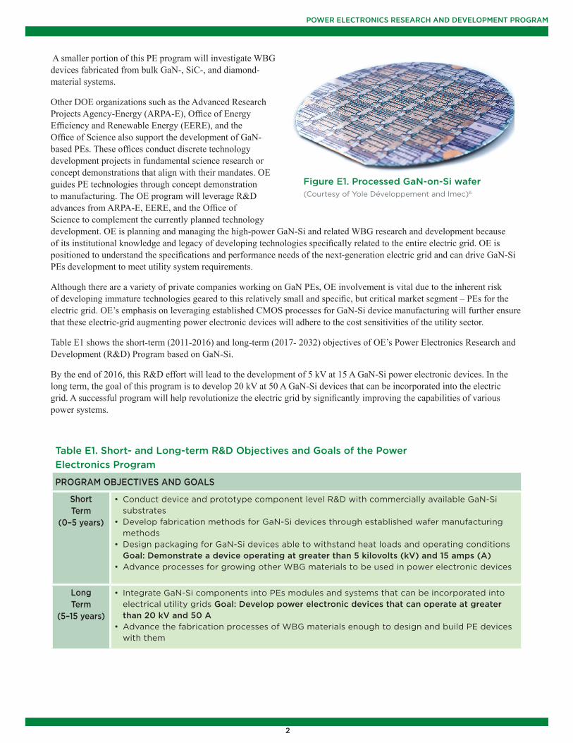
1. Gallium nitride-on-silicon (GaN-Si), a particularly promising WBG semiconductor, is an ordered functional (epitaxial) GaN fi lm on a traditional silicon substrate. This construction allows for unique design architectures and shows signifi cant promise in creating devices for high-power applications. (Figure E1 reveals an example of a processed GaN on silicon wafer).
2. GaN-Si also shows potential to transition to high-volume manufacturing processes because it is amenable to existing semiconductor (complementary metal-oxide-semiconductor, or CMOS) fabrication technology using commercially available, large diameter silicon wafers.5
2
POWER ELECTRONICS RESEARCH AND DEVELOPMENT PROGRAM PLAN
A smaller portion of this PE program will investigate WBG devices fabricated from bulk GaN-, SiC-, and diamond- material systems.
Other DOE organizations such as the Advanced Research Projects Agency-Energy (ARPA-E), Offi ce of Energy Effi ciency and Renewable Energy (EERE), and the Offi ce of Science also support the development of GaN-based PEs. These offi ces conduct discrete technology development projects in fundamental science research or concept demonstrations that align with their mandates. OE guides PE technologies through concept demonstration to manufacturing. The OE program will leverage R&D advances from ARPA-E, EERE, and the Offi ce of Science to complement the currently planned technology development. OE is planning and managing the high-power GaN-Si and related WBG research and development because of its institutional knowledge and legacy of developing technologies specifi cally related to the entire electric grid. OE is positioned to understand the specifi cations and performance needs of the next-generation electric grid and can drive GaN-Si PEs development to meet utility system requirements.
Although there are a variety of private companies working on GaN PEs, OE involvement is vital due to the inherent risk of developing immature technologies geared to this relatively small and specifi c, but critical market segment – PEs for the electric grid. OE’s emphasis on leveraging established CMOS processes for GaN-Si device manufacturing will further ensure that these electric-grid augmenting power electronic devices will adhere to the cost sensitivities of the utility sector.
Table E1 shows the short-term (2011-2016) and long-term (2017- 2032) objectives of OE’s Power Electronics Research and Development (R&D) Program based on GaN-Si.
By the end of 2016, this R&D effort will lead to the development of 5 kV at 15 A GaN-Si power electronic devices. In the long term, the goal of this program is to develop 20 kV at 50 A GaN-Si devices that can be incorporated into the electric grid. A successful program will help revolutionize the electric grid by signifi cantly improving the capabilities of various power systems.
Figure E1. Processed GaN-on-Si wafer (Courtesy of Yole Développement and Imec)6
Table E1. Short- and Long-term R&D Objectives and Goals of the Power Electronics Program
PROGRAM OBJECTIVES AND GOALS
Short Term
(0–5 years)
• Conduct device and prototype component level R&D with commercially available GaN-Si substrates
• Develop fabrication methods for GaN-Si devices through established wafer manufacturing methods
• Design packaging for GaN-Si devices able to withstand heat loads and operating conditions Goal: Demonstrate a device operating at greater than 5 kilovolts (kV) and 15 amps (A)
• Advance processes for growing other WBG materials to be used in power electronic devices
Long Term
(5–15 years)
• Integrate GaN-Si components into PEs modules and systems that can be incorporated into electrical utility grids Goal: Develop power electronic devices that can operate at greater than 20 kV and 50 A
• Advance the fabrication processes of WBG materials enough to design and build PE devices with them

3
U.S. electricity demand is projected to increase by 30% between 2008 and 2035 as the United States transitions to a more digital economy and increases its dependence on electricity.1 Historically, utilities have met demand growth by building infrastructure; however, that approach is limited. Investment in new power lines continues to lag due to economic and regulatory uncertainties while the grid experiences increased congestion, higher vulnerability to cascading failures, and reduced reliability in electric service.9,10,11 Furthermore, today’s grid was not designed to accommodate the current diverse mix of electricity generation sources and the amount of energy generated.
1.1. Solid-State Semiconductor Power ElectronicsFuture electric utility systems are envisioned to be highly automated, interactive “smart” grids that can self-adjust to meet the demand for electricity reliably, securely, and economically. Transforming today’s electric grid to the grid of the future will require creating or advancing a number of technologies, tools, and techniques—specifi cally, the capabilities of power electronics (PE).12 PE devices provide an interface between electrical systems, such as an interconnection of two asynchronous alternating current (AC) systems or a means to convert AC to direct current (DC) and vice versa. Solid-state wide bandgap (WBG) semiconductor electronics (such as silicon carbide [SiC], gallium nitride [GaN], and diamond) are envisioned to improve the reliability and effi ciency of the next-generation grid substantially. This document reviews the strategy for developing WBG PEs, focusing on gallium nitride-on-silicon (GaN-Si).
1.2. The Need for Power Electronics DevelopmentFor the last several decades, silicon (Si)-based semiconductors have been the primary devices used by most, if not all, power applications in the electric grid.13,14 In particular, Si-based, insulated-gate bipolar transistors and gate turn-off thyristors have been the dominant semiconductor switches for utility applications and technology improvements. PE systems can be part of or interact with electric power systems for power fl ow control or interface with generation and storage equipment. Approximately 30% of all electric power currently generated uses PE somewhere between the point of generation and distribution. By 2030, it is expected that 80% of all electric power will fl ow through PE.15 Applications utilizing PE include:
Power Flow Control
• Flexible alternate current transmission system (FACTS) devices (Figure 1)
• High-voltage direct converter stations (HVDC) (Figure 2)
• Static Volt Ampere Reactive (VAR) compensators
• Fault current limiting devices
• Solid-state distribution transformers
• Transfer switches and solid-state circuit breakers
• Active fi lters
Grid Interface
• Plug-in hybrid electric vehicles
• Renewable and distributed energy resources
• Energy storage devices
The U.S. electric grid, built and expanded as demand for power has grown over the last century, now contains more than 200,000 miles of high-voltage transmission lines and 5.5 million miles of local distribution lines, connecting many thousands of generating power plants to factories, homes, and businesses.7 This system is the backbone of the nation’s economy—enabling e-commerce and job creation, powering equipment and communications, and improving quality of life.
1.0. INTRODUCTION
Figure 1. Flexible alternate current transmission system (FACTS) (Courtesy ABB).
POWER ELECTRONICS RESEARCH AND DEVELOPMENT PROGRAM PLAN
4
PEs enable utilities to deliver power to their customers effectively while providing increased reliability, security, and fl exibility to the bulk power system. Some of the benefi ts of using power electronics in electric grid applications include the following:
• Enable power fl ow control—PE devices operate like advanced switches to modulate current fl ow and enable precise control of the electric grid. This allows power to fl ow quickly from one line to another in order to optimize the system.16,17 More control of power fl ow and the ability to integrate more functionality into existing systems (e.g., direct current [DC] converters combined with transformers) will reduce the amount of equipment needed and increase asset utilization.
• Increase transmission and distribution loading—Utilizing the devices’ robust switching capabilities, PEs enable transmission and distribution lines to be loaded more heavily without increasing the risk of disturbances on the system. This can defer the need for new transmission lines.18
• Enable power fl ow to connect electric grids—PE devices enable electricity to fl ow in both directions between grids and allow the grids to absorb or supply power as needed.
• Improve power system transient and dynamic stability—Combining the improvements made in computing power and communications with PE permits the development of wide-area, stable controls for power systems.19
• Enable renewable resource integration—Most renewable energy technologies produce either DC power with various magnitudes or alternating current (AC) power with various magnitudes and frequencies. PE and control equipment are required to convert these into grid-level AC power.20 Other types of power conversion (AC to DC, etc.) will be facilitated by PE.
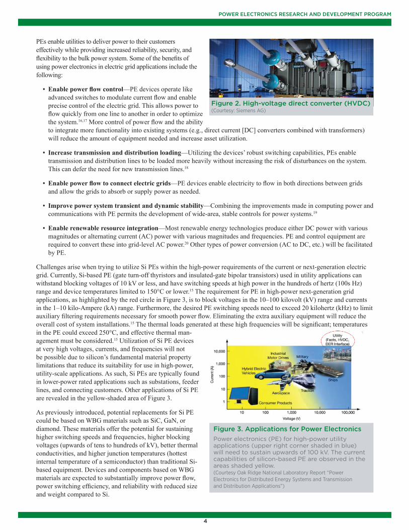
Challenges arise when trying to utilize Si PEs within the high-power requirements of the current or next-generation electric grid. Currently, Si-based PE (gate turn-off thyristors and insulated-gate bipolar transistors) used in utility applications can withstand blocking voltages of 10 kV or less, and have switching speeds at high power in the hundreds of hertz (100s Hz) range and device temperatures limited to 150°C or lower.15 The requirement for PE in high-power next-generation grid applications, as highlighted by the red circle in Figure 3, is to block voltages in the 10–100 kilovolt (kV) range and currents in the 1–10 kilo-Ampere (kA) range. Furthermore, the desired PE switching speeds need to exceed 20 kilohertz (kHz) to limit auxiliary fi ltering requirements necessary for smooth power fl ow. Eliminating the extra auxiliary equipment will reduce the overall cost of system installations.15 The thermal loads generated at these high frequencies will be signifi cant; temperatures in the PE could exceed 250°C, and effective thermal man-agement must be considered.15 Utilization of Si PE devices at very high voltages, currents, and frequencies will not be possible due to silicon’s fundamental material property limitations that reduce its suitability for use in high-power, utility-scale applications. As such, Si PEs are typically found in lower-power rated applications such as substations, feeder lines, and connecting customers. Other applications of Si PE are revealed in the yellow-shaded area of Figure 3.
As previously introduced, potential replacements for Si PE could be based on WBG materials such as SiC, GaN, or diamond. These materials offer the potential for sustaining higher switching speeds and frequencies, higher blocking voltages (upwards of tens to hundreds of kV), better thermal conductivities, and higher junction temperatures (hottest internal temperature of a semiconductor) than traditional Si-based equipment. Devices and components based on WBG materials are expected to substantially improve power fl ow, power switching effi ciency, and reliability with reduced size and weight compared to Si.
Figure 2. High-voltage direct converter (HVDC)(Courtesy: Siemens AG)
Figure 3. Applications for Power ElectronicsPower electronics (PE) for high-power utility applications (upper right corner shaded in blue)will need to sustain upwards of 100 kV. The currentcapabilities of silicon-based PE are observed in the areas shaded yellow. (Courtesy Oak Ridge National Laboratory Report “Power Electronics for Distributed Energy Systems and Transmission and Distribution Applications”)
POWER ELECTRONICS RESEARCH AND DEVELOPMENT PROGRAM PLAN
5
OE’s PE program will investigate other WBG devices fabricated from bulk GaN-, SiC-, and diamond-based PE, but will be a lower priority for the following reasons:
• Producing bulk GaN materials is extremely diffi cult due to its extremely high decomposition pressures and high melting temperature.2
• Reoccurring challenges exist for developing SiC PEs, including defect density control and material availability, despite decades of research.3
• Diamond is perhaps the ultimate material for power devices because of its outstanding electrical properties. However, the diamond manufacturing process is still in its infancy; it is expected that research will yield diamond power devices no sooner than 2–3 decades from now.4
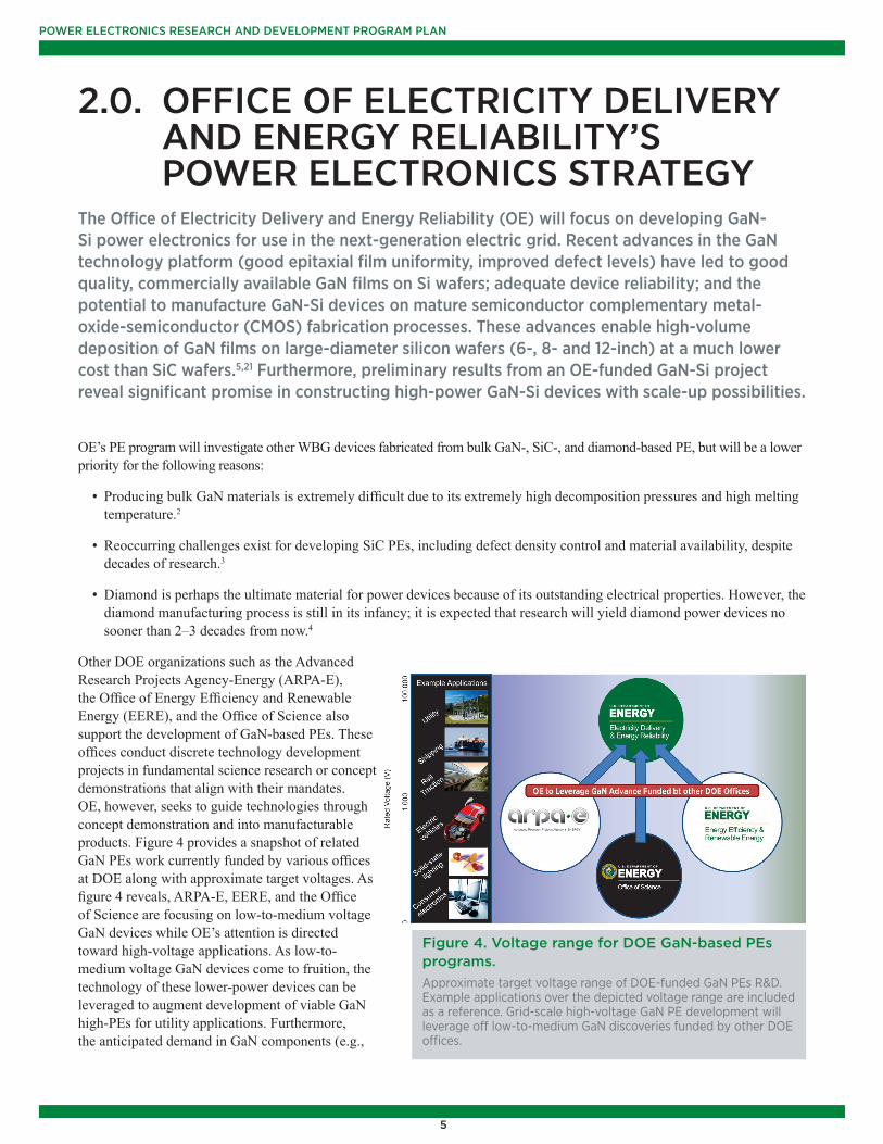
Other DOE organizations such as the Advanced Research Projects Agency-Energy (ARPA-E), the Offi ce of Energy Effi ciency and Renewable Energy (EERE), and the Offi ce of Science also support the development of GaN-based PEs. These offi ces conduct discrete technology development projects in fundamental science research or concept demonstrations that align with their mandates. OE, however, seeks to guide technologies through concept demonstration and into manufacturable products. Figure 4 provides a snapshot of related GaN PEs work currently funded by various offi ces at DOE along with approximate target voltages. As fi gure 4 reveals, ARPA-E, EERE, and the Offi ce of Science are focusing on low-to-medium voltage GaN devices while OE’s attention is directed toward high-voltage applications. As low-to-medium voltage GaN devices come to fruition, the technology of these lower-power devices can be leveraged to augment development of viable GaN high-PEs for utility applications. Furthermore, the anticipated demand in GaN components (e.g.,
The Offi ce of Electricity Delivery and Energy Reliability (OE) will focus on developing GaN-Si power electronics for use in the next-generation electric grid. Recent advances in the GaN technology platform (good epitaxial fi lm uniformity, improved defect levels) have led to good quality, commercially available GaN fi lms on Si wafers; adequate device reliability; and the potential to manufacture GaN-Si devices on mature semiconductor complementary metal-oxide-semiconductor (CMOS) fabrication processes. These advances enable high-volume deposition of GaN fi lms on large-diameter silicon wafers (6-, 8- and 12-inch) at a much lower cost than SiC wafers.5,21 Furthermore, preliminary results from an OE-funded GaN-Si project reveal signifi cant promise in constructing high-power GaN-Si devices with scale-up possibilities.
2.0. OFFICE OF ELECTRICITY DELIVERY AND ENERGY RELIABILITY’S POWER ELECTRONICS STRATEGY
Figure 4. Voltage range for DOE GaN-based PEs programs. Approximate target voltage range of DOE-funded GaN PEs R&D. Example applications over the depicted voltage range are included as a reference. Grid-scale high-voltage GaN PE development will leverage off low-to-medium GaN discoveries funded by other DOE offi ces.
POWER ELECTRONICS RESEARCH AND DEVELOPMENT PROGRAM PLAN

6
switches, converters, power supplies) for widespread use in effi cient lighting, electric vehicles, and other applications will drive down the costs for all GaN starting materials, further improving the potential for commercially viable, utility-rated, GaN-based PE.
OE is planning and managing the high-power GaN-Si and related WBG research and development because of its institutional knowledge and legacy of developing technologies specifi cally related to the entire electrical grid. OE is positioned to better understand the specifi cations and performance needs of the next-generation electric grid and can drive GaN-Si PEs development to meet utility system requirements. Figure 5 shows the program’s two development focus areas (shaded pink) for the short and long terms.
Although a variety of private companies are working on GaN PEs, OE involvement in GaN-Si PEs is vital because industry alone will not drive product development for high-power applications, due to the inherent risk of developing immature technologies geared to this relatively small and specifi c, but critical, market segment. OE research and development for high-power, GaN-Si PE applications will attempt to leverage the GaN technology used in established optoelectronics and radio frequency (RF) applications to further mitigate some of the risk in this relatively new area of development. These GaN devices have been commercially available since the 2000s and are rapidly displacing established products; market sizes for various GaN devices are shown in Figure 6.22 This OE program will also utilize commercially available GaN-Si materials as starting materials for building devices and larger components, thereby limiting much of the need for fundamental materials development.
Figure 7 provides an example of the size and performance improvements a commercially available GaN-Si point-of-load PE device has compared to one produced with silicon. The GaN-Si device is less than one-third the size of the commercially available silicon solution and operates at fi ve times the frequency.23 The OE PE program is expected to deliver GaN-Si based utility PEs with performance improvements and smaller footprints compared to existing Si devices. More importantly, these PE components should increase functionality and provide greater reliability to the electric grid when implemented.
Figure 5. Wide Spectrum of PEs research and development The Power Electronics Research and Development Program will focus on device and component R&D, as indicated by the shaded area
Figure 6. Market size of compound semi devices Compound semiconductor PE market size for various device applications. (Courtesy of Yole Développement)
Figure 7. Gallium nitride-on-silicon devices Can operate at higher frequencies compared to a silicon devices, resulting in smaller size supporting electronic circuit elements and an overall reduction in module size. (Courtesy of International Rectifi er Corp)
POWER ELECTRONICS RESEARCH AND DEVELOPMENT PROGRAM PLAN

7
3.1. VisionThe vision of the OE PE program is to enable highly integrated, cost competitive and reliable PE devices and components to improve functionality, reliability, and effi ciency of next-generation grid components and systems. This will be accomplished by designing and using advanced power semiconductor devices fabricated using GaN-Si WBG materials with unique topologies and architectures and optimized control algorithms. A successful GaN-Si program will help realize a revolutionary new electric grid by improving the capabilities of various power devices found in the utility grid.
3.2. Activity PlanGaN-Si WBG semiconductor PE devices will require signifi cant development efforts over a number of years to prepare them for use in electric grid applications. The activities listed in Table 1 outline the activities for advancing GaN-Si technology. These activities are categorized in three key research areas: design and testing, fabrication and processing improvements, and modeling and packaging. Table 1 shows the milestones for 2012–2016.
Design and Testing
High-voltage WBG semiconductor device design
High-voltage device prototypes need to be built to demonstrate the superiority of WBG GaN-Si technology. Research is needed in device optimization to achieve low losses at higher switching frequencies and to reduce the size of the devices. In addition, devices need to be designed with high-voltage blocking capabilities. WBG starting materials are quite different from Si semiconductors, meaning unique device topologies and architectures can be explored and could potentially uncover novel device performance and capabilities. Designs will be fabricated on commercially available, high-quality, large-area, epitaxial GaN fi lms on large-area Si substrates.
Higher order components
Following the realization of high-voltage PE devices, the next step in the development pathway is to integrate devices to create higher-order PE components. Because GaN-Si WBG materials are relatively new, component geometries are not
The OE Power Electronics Research and Development Program has structured its R&D into several activity areas with specifi c short- and long-term goals. The achievement of these goals will help fulfi ll the vision of the program and OE.
3.0. RESEARCH AND DEVELOPMENT PROGRAM
POWER ELECTRONICS RESEARCH AND DEVELOPMENT PROGRAM PLAN
Table 1. Milestones and Long-term Goal
MILESTONES GOAL
2012 2013 2014 2015 2016 Long-Term
Demonstrate a gallium nitride on silicon (GaN-Si) device that can be operated at a minimum voltage of 1.3 kV, to support the development of grid-scale power electronicsdevices to enhance power fl ow control and grid reliability
Demonstrate 50% improvement in GaN-Si device yield; initiate development of device operating models and packaging designs
Demonstrate higher voltage (>2.5 kV) devices can be built on commercially available GaN-Si wafers
Demonstrate a prototype device operating at greater than 5 kV and 15 A
Demonstrate a GaN-Si module that is cost-effective for one market application and will improve grid reliability; optimize device operating models and packaging
Develop a utility-scale device that can operate at greater than 20 kV and 50 A
8
constrained to those based on designs with silicon. Therefore, device engineers will have full freedom to explore alternative PE structures and assemblies that can perform similar functions as those created on silicon.
Fabrication and Processing Improvements
WBG fi lm fabrication process improvement and wafer process development
GaN WBG semiconductor devices will be designed using GaN epitaxial fi lms on Si substrates. Utilizing GaN-Si has advantages, including reduced energy usage during manufacturing, higher degree of fl exibility in materials manipulation, and reduced costs from the use of readily-available Si substrates.
Furthermore, the use of GaN devices on Si substrates will allow for the leveraging of existing high-volume and well-established Si CMOS manufacturing techniques. Existing Si CMOS equipment infrastructure will be utilized for the manufacturing of GaN-Si components, which can result in substantially lower production costs. Process development will play a signifi cant part in the PE R&D plan to get these devices manufactured in high volume.
Parallel Fabrication Activities
The fi rst generation of GaN PEs device design and fabrication will be epitaxial fi lm-based. However, some effort will be devoted to fabricating WBG semiconductor PEs based on bulk GaN, bulk SiC, and diamond materials. This diversifi ed approach will spread out the development risk and increase the chance of successfully fabricating high-power WBG power electronic devices and components.
Packaging and Modeling
Power electronics packaging and thermal design for use in harsh environments
WBG semiconductors PEs must be properly packaged to ensure safe and reliable operation under demanding conditions such as high temperatures, high voltages and currents, and potentially varying environments. Heat is generated when these power electronic devices are switched between different states; this excess heat must be dissipated using an effective thermal management system, either passive or active. Efforts to identify optimal thermal management methods—ideally air-cooled passive systems—will be sought.
Higher order device and module modeling, production, and characterization
As the new GaN-Si PE devices (and others) become available, modeling efforts will need to continue evolving. The physics of WBG power devices are probably different enough from Si PEs that existing models will most likely not be able to accurately represent the behavior of GaN-Si devices. This OE program will develop GaN-Si device behavior models as necessary. Testing and characterizing components will then be needed to prove the validity of these models. The behavior of GaN power electronic components can then be put into utility system models to determine their suitability for integration into the current and next-generation electric grid.
Long-term Tasks
The tasks above identify a pathway toward creating viable PEs components. The longer-term tasks identifi ed below are required to transition PEs components into systems and, ultimately, into the next-generation electric grid.
• Accurate package design to house PEs components in larger systems so that they can withstand not only the thermal loads these devices are expected to create, but also the types of operating environments they will be placed into
• Reliable testing of PEs devices and components to meet various standards required by the utility industry
• Development of GaN-Si PE components into PE systems and associated control systems to drive optimized power control
• Interaction and interoperability modeling of GaN-Si PEs systems in electric grid applications to understand how they will behave and impact the electric grid
POWER ELECTRONICS RESEARCH AND DEVELOPMENT PROGRAM PLAN
9
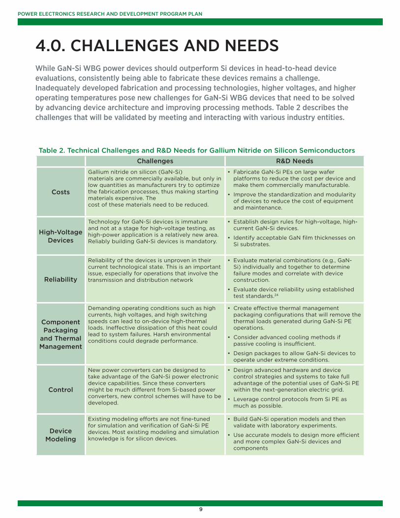
While GaN-Si WBG power devices should outperform Si devices in head-to-head device evaluations, consistently being able to fabricate these devices remains a challenge. Inadequately developed fabrication and processing technologies, higher voltages, and higher operating temperatures pose new challenges for GaN-Si WBG devices that need to be solved by advancing device architecture and improving processing methods. Table 2 describes the challenges that will be validated by meeting and interacting with various industry entities.
4.0. CHALLENGES AND NEEDS
POWER ELECTRONICS RESEARCH AND DEVELOPMENT PROGRAM PLAN
Table 2. Technical Challenges and R&D Needs for Gallium Nitride on Silicon Semiconductors
Challenges R&D Needs
Costs
Gallium nitride on silicon (GaN-Si)materials are commercially available, but only in low quantities as manufacturers try to optimize the fabrication processes, thus making starting materials expensive. The cost of these materials need to be reduced.
• Fabricate GaN-Si PEs on large wafer platforms to reduce the cost per device and make them commercially manufacturable.
• Improve the standardization and modularity of devices to reduce the cost of equipment and maintenance.
High-Voltage Devices
Technology for GaN-Si devices is immature and not at a stage for high-voltage testing, as high-power application is a relatively new area. Reliably building GaN-Si devices is mandatory.
• Establish design rules for high-voltage, high-current GaN-Si devices.
• Identify acceptable GaN fi lm thicknesses on Si substrates.
Reliability
Reliability of the devices is unproven in their current technological state. This is an important issue, especially for operations that involve the transmission and distribution network
• Evaluate material combinations (e.g., GaN-Si) individually and together to determine failure modes and correlate with device construction.
• Evaluate device reliability using established test standards.24
Component Packaging
and Thermal Management
Demanding operating conditions such as high currents, high voltages, and high switching speeds can lead to on-device high-thermal loads. Ineffective dissipation of this heat could lead to system failures. Harsh environmental conditions could degrade performance.
• Create effective thermal management packaging confi gurations that will remove the thermal loads generated during GaN-Si PE operations.
• Consider advanced cooling methods if passive cooling is insuffi cient.
• Design packages to allow GaN-Si devices to operate under extreme conditions.
Control
New power converters can be designed to take advantage of the GaN-Si power electronic device capabilities. Since these converters might be much different from Si-based power converters, new control schemes will have to be developed.
• Design advanced hardware and device control strategies and systems to take full advantage of the potential uses of GaN-Si PE within the next-generation electric grid.
• Leverage control protocols from Si PE as much as possible.
Device Modeling
Existing modeling efforts are not fi ne-tuned for simulation and verifi cation of GaN-Si PE devices. Most existing modeling and simulation knowledge is for silicon devices.
• Build GaN-Si operation models and then validate with laboratory experiments.
• Use accurate models to design more effi cient and more complex GaN-Si devices and components

10
5.1 Public–Private PartnershipsThe OE Power Electronics Research and Development Program’s strategy is simple: engage world-class professionals from key public and private organizations for thought leadership to craft the PE activity plan and direction in order to meet the energy goals of DOE and the nation. The program’s stakeholders are the electric utilities and manufacturers of PEs for utility applications, including thise organizations that interface with energy storage and renewable energy systems. Additional partners include electricity consumers, project developers, and state and regional agencies.
Electric utility stakeholders include investor-owned and public utilities; electric cooperatives; and federal utilities, such as the Tennessee Valley Authority, Bonneville Power Administration, and Western Area Power Administration. The involvement of utilities and other industry will ensure that technologies developed by this program are relevant and easily integrated into the electric grid.
The PE R&D program will leverage federal resources and partner with co-sponsors on technical research initiatives led by the nation’s most technically capable organizations and individuals, thus achieving the best returns on taxpayer investments. Research partners include but are not limited to the following:
• Universities
• Industry research organizations
• National laboratories
• Utilities
• State energy research and development agencies
• Federal sponsoring agencies
- Department of Homeland Security
- Department of Energy
- Department of Defense
- Other agencies that will benefi t from PEs development
Appendix 1 provides a sample of active program areas and agencies supporting PE work. Within DOE, ARPA-E and EERE have awarded a series of GaN projects to develop capabilities for use in electric vehicles; solid-state lighting; compact motors and inverters; and voltage regulators for powering future generations of microprocessors, graphics cards, and memory devices.25 In DOE’s Offi ce of Science Small Business Innovation Research program, projects aim to advance the fabrication of white-light, light-emitting diodes (LEDs) based on GaN.26
The Department of Defense’s Defense Advanced Research Projects Agency and the other military research laboratories (Army, Air Force, and Navy) are also working on a variety of GaN-based components for military and national security applications, including power amplifi cation and analog-to-digital converters.27,28 The Department of Homeland Security is involved in developing GaN components for use in the detection and analysis of chemical and biological agents.29 OE will track the progress of these various GaN development efforts and transition relevant accomplishments when possible.
Building and maintaining effective public–private partnerships is one of the key strategies for achieving the objectives of the Power Electronics Research and Development Program and the mission, vision, and goals of OE. Such partnerships facilitate increased R&D and enable industry to capitalize on the outcomes.
5.0. PARTNERSHIP STRATEGIES
POWER ELECTRONICS RESEARCH AND DEVELOPMENT PROGRAM PLAN
11
By providing appropriate, long-term support to these OE PE R&D areas, OE will ensure that PE products and solutions can be developed to meet program goals and enable the next-generation electric grid. The engagement of public-private partnerships for the PE program will take the following two forms:
1. Technical exchanges will be made through periodic conferences, workshops, annual peer reviews, informal meetings, and joint R&D planning sessions.
2. Communication and outreach between partners will be achieved through websites, webcasts, and technical journals to foster information sharing and technology transfer.
Cost-shared R&D projects are another critical form of partnership within the PE program. To enhance the value of such projects, the program will build partnerships with other sponsoring organizations—both public and private—to leverage resources that are focused on accomplishing tasks of mutual interest. OE will use competitive solicitations to engage the nation’s top R&D performers to design, fabricate, laboratory test, fi eld test, and demonstrate new technologies, tools, and techniques. The cost-sharing requirements for these types of cooperative agreements are specifi ed in the Energy Policy Act of 1992.
Another mechanism for engaging researchers will be Small Business Innovation Research program grants, which can be used by federal agencies to nurture innovative concepts from small businesses. Universities, industry, and national laboratories will play key roles in the PE program activities. Targeted capabilities at universities and national laboratories will be applied to program management and implementation, as well as to research needs that require specifi c scientifi c and engineering talent.
5.2. Translating Innovation into Commercial ProductsDOE is investing in high-impact research that can lead to a clean economy and solve our energy challenges. OE will work across the department to ensure that key program initiatives in the Offi ce of Science, EERE, and ARPA-E program achieve success in translating innovative concepts to the marketplace. The Energy Frontier Research Centers within the Offi ce of Science aim to achieve fundamental scientifi c discoveries that are relevant to real-world problems. Research activities within the Energy Frontier Research Centers are typically limited to the discovery phase of the technology development process. ARPA-E projects are more technology-oriented and involve high-impact activities that are deemed too risky for initial industrial investments alone. With a two- to three-year time frame, APRA-E projects are typically limited to feasibility demonstrations, process validation, or prototype development. As such, a gap exists between discovery and commercialization that must be bridged in order to provide a reasonable return on taxpayers’ investments.
OE has a successful track record of shepherding fundamental scientifi c understanding through applied materials and technology R&D to product development and commercialization. The OE PE program is therefore a natural receptacle of DOE successes in this subject matter. By absorbing the best-of-the-best projects and providing appropriate long-term support, the OE program will ensure that innovative power electronic products and solutions will be available and accepted into the marketplace.
POWER ELECTRONICS RESEARCH AND DEVELOPMENT PROGRAM PLAN
12
These management areas combine to guarantee that the program effectively serves industry, government, and the public. This program follows a multi-step planning and management process designed to ensure that all funded technical R&D projects are chosen based on their qualifi cations in meeting clearly defi ned criteria. This process entails the following:
• Offer competitive solicitations for fi nancial assistance awards and national lab R&D
• Conduct peer reviews of proposals looking to meet the Funding Opportunity Announcement goals, objectives, and performance
• Perform peer reviews of in-progress projects every two years on the scientifi c merit, likelihood of technical and market success, actual or anticipated results, and cost effectiveness of research management—evaluation results will cycle back to program planning and portfolio management
• Conduct stage gate reviews to determine the readiness of a technology or activity to advance to the next phase of development, pursue alternative paths, or be terminated; readiness reviews will be conducted on an as-needed schedule based on project progression in meeting the established stage gate criteria
• Provide annual OE internal reviews of the program to ensure continuous improvements and proper alignment with R&D priorities and industry needs
• Make apparent the value of R&D projects, individually and collectively, to achieving the program goal and targets by applying this management process consistently throughout the program; the value of these projects will be publicized through program communications to the industry, the public, and other smart-grid stakeholder organizations
The following principal areas of portfolio development and program management are integral to the OE Power Electronics Research and Development Program:
• Communication of the program
• Analysis of the program
• Evaluation of the program
• Technology transfer
6.0. PORTFOLIO DEVELOPMENT AND MANAGEMENT
POWER ELECTRONICS RESEARCH AND DEVELOPMENT PROGRAM PLAN
13
This list is not meant to be exhaustive, but rather a representation of the current and completed work.
APPENDIX A. SUMMARY OF FEDERAL GALLIUM NITRIDE DEVELOPMENT WORK
POWER ELECTRONICS RESEARCH AND DEVELOPMENT PROGRAM PLAN
AgencyProject
(Prime performer)Synopsis
DOE Advanced Research Projects Agency–Energy (ARPA-E)
Switches—Automobiles: Gallium Nitride (GaN) Switch Technology for Bi-directional Battery-to-Grid Charger Applications (HRL Laboratories, LLC)
This project develops effi cient, high-power, and cost-effective power converters that apply to the automotive sector. Specifi cally, it will utilize high-voltage GaN- low-cost silicon (Si) substrate switches operating at megahertz frequencies.
Advanced Technologies for Integrated Power Electronics (Massachusetts Institute of Technology)
This project targets radical improvements in the size, integration, and performance of power electronics for high-effi ciency, solid-state lighting with a focus on circuits for interfacing with grid-scale voltages (>100 volts [V]) at power levels of 10–100 watts (W). Specifi cally, it will develop GaN-Si power devices, nano-structured magnetic materials and microfabricated magnetic components, and high-frequency power conversion circuits.
High-Performance, GaN High-Electron Mobility Transfer Modules for Agile Power Electronics (Transphorm Inc)
This project enables compact motor drives and grid-tied inverters operating at high power (3–10 kilowatts [kW]) with effi ciency greater than 96%. It will develop the fi rst hybrid multichip power modules for inverters and converters operating at high frequency (1 megahertz [MHz]), using low-loss, ultra-fast GaN-Si power switches that are normally in off mode.
Power Supplies on a Chip (Virginia Tech)
This technology will replace the current power management voltage regulators for powering the future generations of microprocessors, graphics cards, and memory devices. A 3-D integrated power supplies on a chip will be developed using chip-scale integration of a new generation of GaN-Si devices with high-frequency soft magnetic material.
Advanced Power Semiconductor and Packaging (Delphi Automotive Systems LLC)
Developing a novel electrical energy conversion device that will be 50% more effi cient than existing silicon-based technologies. This device will consist of a 600 V GaN device combined with sintered interconnects and double-sided cooling.
Ammonothermal Bulk GaN Crystal Growth for Energy Effi cient Lighting (Momentive Performance Materials)
Lighting consumes a signifi cant percentage of total energy production. Momentive Performance Materials (MPM) is developing GaN solid-state lighting that is more effi cient at generating light and produces minimal waste heat. MPM has already demonstrated a high-pressure, high-temperature process to grow single-crystal GaN material with low defects.
14
APPENDIX A. SUMMARY OF FEDERAL GALLIUM NITRIDE DEVELOPMENT WORK
POWER ELECTRONICS RESEARCH AND DEVELOPMENT PROGRAM PLAN
AgencyProject
(Prime performer)Synopsis
DOE Offi ce of Science
Development of Fabrication Techniques for High Extraction Effi ciency, Bulk GaN-Based Light-Emitting Diodes (Soraa, Inc.)
This project will develop novel manufacturing techniques for next-generation GaN-based LEDs, enabling, for the fi rst time, high-brightness LEDs across the visible spectrum that can be implemented into future energy effi cient white lighting solutions.
DOE Offi ce of Energy Effi ciency and Renewable Energy—Building Technologies Program
Epitaxial Growth of GaN-Based LED Structures on Sacrifi cial Substrates(Georgia Institute of Technology)
Develop high-effi ciency LED devices that will lead to higher external quantum effi ciency performance, better electrostatic discharge durability, simple low-cost fabrication, high product yield with high brightness, and better heat management. A sacrifi cial substrate will be used for device growth that can easily be removed using a wet chemical etchant leaving only the GaN epi-layer and possibly a very thin (~1mm) intermediate substrate.
High-Effi ciency Non-Polar GaN-Based LEDs(Inlustra Coporation)
Better understanding the factors that affect III-nitride LED internal quantum effi ciency (IQE), and maximizing IQE in blue and green HB-LEDs based on non-polar (Al,In)GaN fi lms. The objectives of this project center on the development of HB-LED active regions with high internal quantum effi ciency, for immediate application in advanced solid-state light engines that are suitable for general illumination.
High-Effi ciency Nitride-Based Photonic Crystal Light Sources(University of California, Santa Barbara)
Development of novel GaN-based LED structures for use in advanced solid-state light engines which are suitable for general illumination.
Low-Cost Substrates for High-Performance Nanorod Array LEDs(Purdue University)
This project is designed to exploit the relief of lattice mismatch strain and the expulsion of dislocations that are characteristic of nanoheteroepitaxy in the growth of heteroepitaxial device structures on nanoscale substrates to expand the spectral range of effi cient GaN-based LEDs to include the entire visible spectrum, thereby eliminating the effi ciency losses associated with phosphor down-conversion.
Novel Heterostructure Designs for Increased Internal Quantum Effi ciencies (IQE) in Nitride LEDs(Carnegie Melon University)
Conduct research concerned with theoretical experimental investigations regarding the infl uence on the density of non-radiative channels and IQE of (a) graded and relaxed InGaN buffer layers having the fi nal composition of the InGaN quantum well (QW) to suppress any negative aspects of polar fi elds in the action region; (b) dislocations and their reduction in the InGaN buffer layers and the QWs; (c) number of quantum wells and the dependence of the effi ciency as a function of injection into these wells; (d) enhanced polarization-based p-type doping and hole injection levels at Ohmic contacts; (e) the use of novel heterostructure design to funnel carriers into the active region for enhanced recombination effi ciency and elimination of diffusion beyond this region; and (f) the fabrication and characterization of blue and green LEDs with enhanced IQE.
15
APPENDIX A. SUMMARY OF FEDERAL GALLIUM NITRIDE DEVELOPMENT WORK
POWER ELECTRONICS RESEARCH AND DEVELOPMENT PROGRAM PLAN
AgencyProject
(Prime performer)Synopsis
DOE Offi ce of Energy Effi ciency and Renewable Energy—Building Technologies Program
Improved InGaN Epitaxial Quality by Optimizing Growth Chemistry (Sandia National Laboratories)
Develop high-effi ciency green (530 nm) light emitters based on improvement in InGaN epitaxial material quality.
Multicolor, High-Effi ciency, Nanotextures LEDs(Yale University)
Create a new class of active medium with an amplifi ed radiation effi ciency capable of near-unity electron-to-photon conversion for solid-state lighting applications with InGaN.
GaN-Ready Aluminum Nitride Substrates for Cost-Effective, Very Low Dislocation Density III-Nitride LEDs(Crystal IS, Inc.)
Develop and then demonstrate the effi cacy of a cost-effective approach for a low-defect-density substrate on which AlInGaN LEDs can be fabricated. The effi cacy of this “GaN-ready” substrate will then be tested by growing high-effi ciency, long-lifetime InxGa1-xN blue LEDs.
Novel Defect Spectroscopy of InGaN Materials for Improved Green LEDs (Sandia National Laboratories)
Develop a novel quantitative, nanoscale depth-resolved deep-level defect spectroscopy methodology applicable to InGaN thin fi lms like those found in the active regions of InGaN/GaN green LEDs and to LEDs themselves.
Enhancement of Radiative Effi ciency with Staggered InGaN Quantum Well Light Emitting Diodes(Lehigh University)
Improve the intrinsic quantum effi ciency of InGaN-based LEDs for the green spectral region, in particular addressing issues due to the poor wave function overlap from the existence of polarization fi elds inside the quantum well (QW) active regions.
DoD Defense Advanced Research Projects Agency (DARPA)
Wide Bandgap - RF This project is exploring GaN-silicon carbide (SiC) technology to wideband power amplifi er Monolithic Microwave Integrated Circuits (MMICs) for radio frequency (RF) applications.
Disruptive Manufacturing Technologies (BAE Systems)
This project will replace high-power traveling wave tube amplifi ers (TWTAs) (in electronic and information warfare, radar, and communication) with lower cost solid-state GaN components.
Nitride Electronic NeXt Generation Technology (TriQuint Semiconductor)
GaN transistors and integrated circuit technology developments will enable high-performance analog-to-digital converters for future advanced electronic systems.
Wide Band Gap Semiconductor Technology Initiative
The goals of this project are to (1) scale up to 4 cm high-quality SiC substrates, (2) develop alternative substrates, (3) develop uniform aluminum gallium nitride High Electron Mobility Transfer epitaxial growth, and (4) examine materials and device correlations.
Deep Ultraviolet Avalanche Photodetectors
Demonstrate avalanche photodiodes (APDs) operating in Geiger mode. The APDs will operate in the ultraviolet (in the band centered at 280 nm) and will be insensitive to the solar fl ux with a cutoff ratio greater than 106. A short-wavelength-pass fi lter may be inserted in front of the device in order to assure solar blindness. Two classes of materials, silicon carbide (SiC) and aluminum gallium nitride (AlGaN), are being considered for this device.
16
APPENDIX A. SUMMARY OF FEDERAL GALLIUM NITRIDE DEVELOPMENT WORK
AgencyProject
(Prime performer)Synopsis
DoD Defense Advanced Research Projects Agency (DARPA)
Compound Semiconductor Materials On Silicon
Develop a viable process for the fi ne-scale heterogeneous integration of compound semiconductor (CS) devices with standard Si CMOS, and establish that this integration enables superior performance in specifi c mixed-signal circuit demonstrators. The program will focus on four major technical areas of interest: placement of CS devices, heterogeneous integration, dense heterogeneous interconnects, and yield enhancement.
Army Research Laboratory (ARL)
Rare-earth Doped GaN—An Innovative Path Toward Areascalable
Solid-state High Energy Lasers Without ThermalDistortion
Develop a new approach to highly scalable diodepumped solid-state lasers based on rare-earth (RE) neodymium (Nd3+) doping of gallium nitride (GaN), a high thermal conductivity material, with the goal of fully eliminating the bottleneck in the heat removal process associated with the low thermal conductivity of the gain medium compared to that of heat-sinking materials.
Offi ce of Naval Research (ONR)
Department of Defense Multidisciplinary University Research Initiative, Fundamental Study of High- and Low- Dielectrics for III-V Electronic Devices
This project researches alternative high- and low-K dielectrics for use in III-V electronics technologies. The goals are to (1) develop a detailed understanding of the fundamental properties of these dielectrics, (2) investigate approaches to control these properties, and (3) expand understanding of how the properties of the dielectrics impact device performance (how they can be tailored to achieve the desired device performance).
Air Force Research Laboratories (AFRL)
Various Projects Develop new GaN modules for unmanned aerial vehicles with 20 W and 50 W amplifi ers. A challenging aspect of the program includes fi tting new 20 W amplifi ers into the same space now occupied by the fl eet’s existing 1 W devices that limit the range and broadcast power of the aircraft
Design AlGaN/GaN high electron mobility transistors (HEMTs) on free-standing chemical-vapor-deposited (CVD) diamond substrate wafers.
National Institute of Standards and Technology (NIST)
GaN “Pin art” on silicon This project is a step toward reliable mass production of semiconductor nano-wires for millionths-of-a-meter scale devices such as sensors and lasers.
National Science Foundation (NSF)
Zinc Oxide (ZnO)/GaN Heterostructure-based Novel Acousto-electronic Devices
This project studies the acousto-electrical interaction in ZnO/GaN heterostructures and develops the tunable devices that comprise a piezoelectric ZnO layer and a polar semiconductor ZnO/GaN heterostructure.
POWER ELECTRONICS RESEARCH AND DEVELOPMENT PROGRAM PLAN
17
APPENDIX B. ACRONYMS AND ABBREVIATIONS
POWER ELECTRONICS RESEARCH AND DEVELOPMENT PROGRAM PLAN
Acronyms Meaning
A amp
ARPA-E Advanced Research Projects Agency-Energy
DOE U.S. Department of Energy
GaN gallium nitride
GaN-Si gallium nitride on silicon
kHz kilohertz
kV kilovolts
kW kilowatts
LED light-emitting diode
MHz megahertz
OE Office of Electricity Delivery and Energy Reliability
PE power electronics
R&D research and development
Si silicon
SiC silicon carbide
V volts
W watt
WBG wide bandgap
ZnO zinc oxide
18
Objective: Develop and Commercialize GaN-based Power Electronic Devices for Grid Applications
Team members and development areas:
• MIT - Device topology and design
• MIT Lincoln Laboratory (LL) – Establishing material–performance relationships/ process development
• M/A-COM Technology Solutions (MACT) – Addressing fundamental manufacturing challenges
Results to Date:
• MIT identifi ed device designs/topologies for GaN on Silicon >1000 V power switching devices
• LL improved epitaxy processing, resulting in smooth, uncracked GaN fi lms ~220 μm thick with good yield
• MACT
1. Completed comprehensive investigation of device isolation techniques and buffer breakdown
2. Demonstrated that >1300V Two Terminal breakdown is achievable in GaN on silicon
3. Completed GaN high-voltage device mask incorporating:
APPENDIX C. ON-GOING POWER ELECTRONICS STUDY: GALLIUM NITRIDE (GAN)INITIATIVE FOR GRID APPLICATION (GIGA)
- Buffer breakdown monitoring
- Ohmic and schottky drain
- Array of discrete power devices
- MIT’s E-mode structure
POWER ELECTRONICS RESEARCH AND DEVELOPMENT PROGRAM PLAN
19
1 U.S. Energy Information Administration, Annual Energy Outlook 2010 (Washington, DC: U.S. Energy Information Administration, 2010), 65–69, http://www.eia.doe.gov/oiaf/aeo/pdf/trend_3.pdf.
2 X.L. Chen, “Growth of bulk GaN single crystals by fl ux method,” Science and Technology of Advanced Materials 6 (2005): 766–771, http://iopscience.iop.org/1468-6996/6/7/A10/pdf/1468-6996_6_7_A10.pdf.
3 Dr. Mike Cooke, “Seeking Workable Low-cost Silicon Carbide,” Semiconductor Today: Compounds and Advanced Silicon 2, no. 9 (November 2007), http://c9corp.com/articles/st54-57.pdf (accessed September 9, 2010).
4 B. Ozpineci, M.S. Chinthavali, and L.M. Tolbert, Enhancing Power Electronic Devices with Wide Bandgap Semiconductors, (Oak Ridge, TN: Oak Ridge National Laboratory, 2007), http://www.ornl.gov/info/ornlreview/v40_2_07/2007_msc_enhancing_pwr.pdf (accessed August 28, 2010)
5 Michael A. Briere, “GaN-based power devices offer game-changing potential in power-conversion electronics,” EE Times, December 30, 2008, http://www.eetimes.com/design/automotive-design/4010344/GaN-based-power-devices-offer-game-changing-potential-in-power-conversion-electronics.
6 “Dow Corning joins the imec GaN affi liation program” January 2011 http://www.i-micronews.com/news/Dow-Corning-joins-imec-GaN-affi liation-program,6305.html (accessed 31 January 2011)
7 Jennifer Weeks and The Daily Climate, “U.S. Electrical Grid Undergoes Massive Transition to Connect to Renewables,” Scientifi c American, April 28, 2010, http://www.scientifi camerican.com/article.cfm?id=what-is-the-smart-grid&print=true.
8 NPR, “Visualizing The U.S. Electric Grid,” NPR, http://www.npr.org/templates/story/story.php?storyId=110997398.
9 JR Minkel, “The 2003 Northeast Blackout—Five Years Later,” Scientifi c American, August 13, 2008, http://www.scientifi camerican.com/article.cfm?id=2003-blackout-fi ve-years-later.
10 Edison International, “Edison Int’l Chairman: Smart Grid Technologies Could Prevent Cascading Regional Blackouts,” Transmission and Distribution World, May 3, 2007, http://tdworld.com/distribution_management_systems/edison-international-smart-grid-congress/.
11 Larry Dignan, “The U.S. electrical grid: How big of a cyber target is it?” ZDNet, April 8, 2009,http://www.zdnet.com/blog/btl/the-us-electrical-grid-how-big-of-a-cyber-target-is-it/16001.
12 Offi ce of Electricity Delivery and Energy Reliability, Research and Development Multi-Year Plan, 2012-2016 (Washington, DC: U.S. Department of Energy, in-progress 2010).
13 Electric Power Research Institute, ”Solid-State Power Electronics: Silicon Carbide (SiC) Switches,” (Palo Alto, CA: Electric Power Research Institute, January 2006), http://mydocs.epri.com/docs/public/000000000001013093.pdf.
14 “Power Electronics Teaching Factory,” Empfasis, January 2001, http://www.empf.org/empfasis/jan01/power101.htm.
15 L. M. Tolbert, et al., Power Electronics for Distributed Energy Systems and Transmission and Distribution Applications: Assessing the Technical Needs for Utility Applications (Oak Ridge, TN: Oak Ridge National Laboratory, 2005), http://www.ece.utk.edu/~tolbert/publications/ornl_tm_2005_230.pdf.
16 The Electricity Innovation Institute, An EPRI Affi liate, Assessment of Proposed CEIDS R&D Project on Power Electronics-Based Controllers (Palo Alto, CA: Steering Committee of the Consortium for Electric Infrastructure to Support a Digital Society, March 21, 2003), http://www.epri-intelligrid.com/intelligrid/docs/Power_Electronics_Assessment.pdf.
17 Justin Gerdes, “The Future of Smart Grid Transmission: Superconducting High-Voltage Power Lines,” Gigaom, February 23, 2010, http://earth2tech.com/2010/02/23/the-future-of-smart-grid-transmission-superconducting-high-voltage-power-lines/.
18 ABB Inc., Energy Effi ciency in the Power Grid, (Norfolk, CA: ABB Inc., 2007), http://www02.abb.com/global/seitp/seitp202.nsf/c71c66c1f02e6575c125711f004660e6/64cee3203250d1b7c12572c8003b2b48/$FILE/Energy+effi ciency+in+the+power+grid.pdf.
APPENDIX D. REFERENCES
POWER ELECTRONICS RESEARCH AND DEVELOPMENT PROGRAM PLAN

20
APPENDIX D. REFERENCES
19 Anjan Bose, “Power System Stability: New Opportunities for Control,” in Stability and Control of Dynamical Systems and Applications, ed. Derong Liu and Panos J. Antsaklis (Boston: Birkhäuser, 2003), http://www.gridstat.net/publications/Bose-GridComms-Overview-Chapter.pdf.
20 Muhammad H. Rashid, “Power Electronics for Renewable Energy Sources” in Power Electronics Handbook: Devices, Circuits and Applications, Second Edition, ed C. V. Nayar S. M. Islam H. Dehbonei K. Tan (Perth, Elsevier Inc. 2007), http://www.globalspec.com/reference/24573/203279/chapter-27-power-electronics-for-renewable-energy-sources.
21 Michael Briere, “GaN-Based Power Device Platform,” Power Systems Design North America, January/February 2009, http://www.powersystemsdesign.com/2009/na/JanFeb/power_conversion.pdf (accessed September 1, 2010; page now discontinued).
22 Richard Stevenson, “IQE prepares to thrive in a buoyant market,” Compound Semiconductor, February 1, 2010, http://compoundsemiconductor.net/csc/features-details.php?id=19597331.
23 Oleg Khaykin, Tim McDonald, Tim Phillips, “International Rectifi er Corp GaNpowIR™ Investor Presentation,” presented on February 23, 2010, http://www.irf.com/investor/GaN_investor_presentation.pdf (accessed August 15, 2010).
24 North American Electric Reliability Corporation, “Reliability Standards,” http://www.nerc.com/page.php?cid=2|20 (accessed August 15, 2010).
25 “DOE Awards $13.4 million to GaN Research,” Compound Semiconductor, July 13, 2010, http://compoundsemiconductor.net/csc/news-details.php?cat=news&id=19732121 (accessed August 15, 2010).
26 U.S. Department of Energy, Offi ce of Science, “DOE SBIR and STTR Phase I Grant Applications Selected for FY 2009 Awards,” http://www.er.doe.gov/sbir/Files/FY09State/CA.html (accessed August 15, 2010).
27 TriQuint Semiconductor, “TriQuint Wins US Air Force Contract to Design, Build GaN Modules for New Drone Aircraft,” BusinessWire, May 23, 2010, http://eon.businesswire.com/news/eon/20100523005059/en (accessed August 15, 2010).
28 Michael Wraback and Mark Dubinskiy, Rare-earth Doped GaN – An Innovative Path Toward Area-scalable Solid-state High Energy Lasers Without Thermal Distortion (2nd year), (Adelphi, MD: Army Research Lab, June 2010), http://www.arl.army.mil/arlreports/2010/ARL-TR-5213.pdf.
29 “Laser diodes with world’s shortest wavelength for bioterror detection,” Homeland Security Newswire, November 29, 2007, http://homelandsecuritynewswire.com/laser-diodes-worlds-shortest-wavelength-bioterror-detection?page=0,0 (accessed August 15, 2010).
POWER ELECTRONICS RESEARCH AND DEVELOPMENT PROGRAM PLAN

21
POWER ELECTRONICS RESEARCH AND DEVELOPMENT PROGRAM PLAN

Printed with a renewable-source ink on paper containing at least 50% wastepaper, including 10% post-consumer waste.
April 2011
www.oe.energy.gov