oled 3.12” - 256x64 dots - lcd-module.com · zeppelinstrasse 19 d-82205 gilching fon...
TRANSCRIPT
Zeppelinstrasse 19 D-82205 Gilching Fon +49-8105-778090 [email protected] http://www.lcd-module.de
5.2018
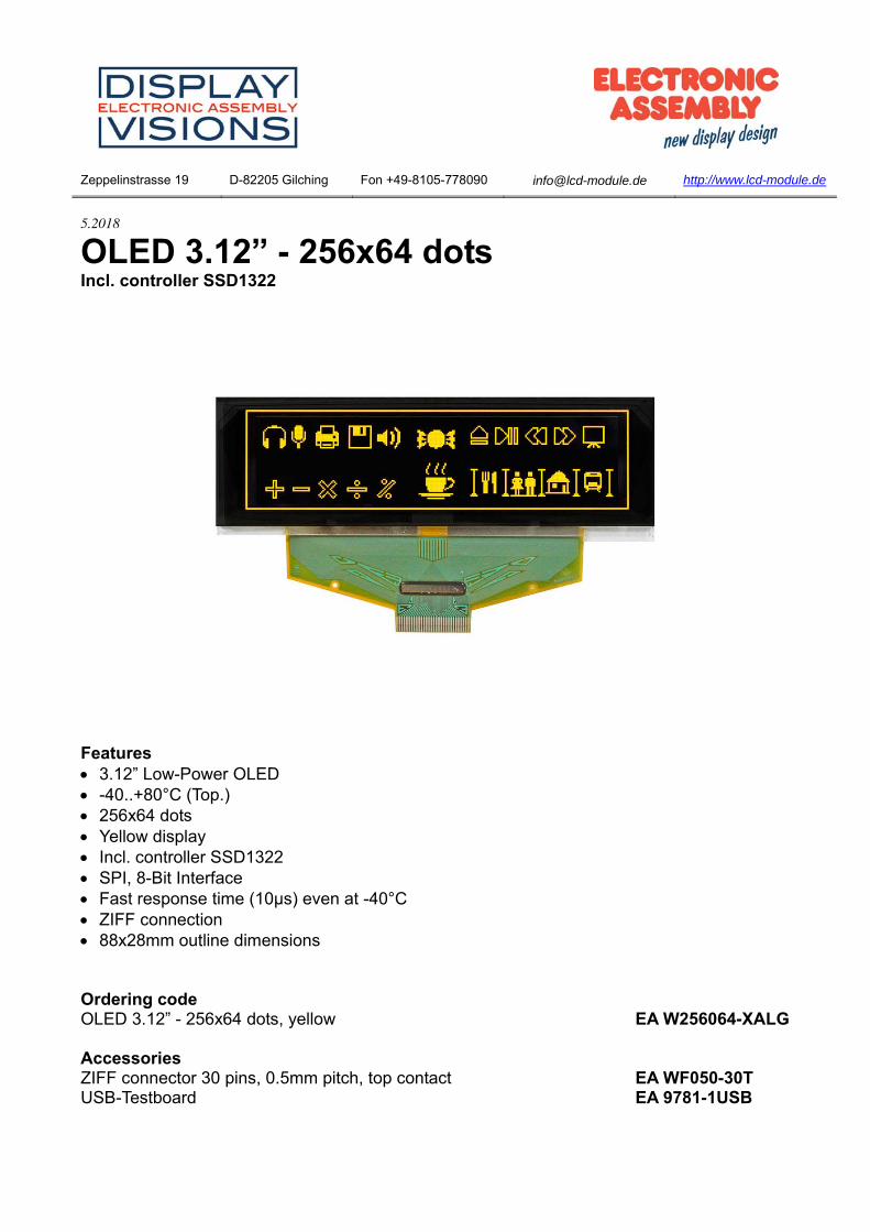
OLED 3.12” - 256x64 dots Incl. controller SSD1322
Features 3.12” Low-Power OLED -40..+80°C (Top.) 256x64 dots Yellow display Incl. controller SSD1322 SPI, 8-Bit Interface Fast response time (10µs) even at -40°C ZIFF connection 88x28mm outline dimensions Ordering code OLED 3.12” - 256x64 dots, yellow EA W256064-XALG Accessories ZIFF connector 30 pins, 0.5mm pitch, top contact EA WF050-30T USB-Testboard EA 9781-1USB
Zeppelinstrasse 19 D-82205 Gilching Fon +49-8105-778090 [email protected] http://www.lcd-module.de
EA W256064-XALG Page 2
Content 1.General Specification
2.Contour Drawing & Block Diagram
3.Interface Pin Function
4.Absolute Maximum Ratings
5.Electrical Characteristics
6.Optical Characteristics
7.OLED Lifetime
8.Reliability
9.Inspection specification
10.Precautions in use of OLED Module
11.Initialization example
12. Application example
Zeppelinstrasse 19 D-82205 Gilching Fon +49-8105-778090 [email protected] http://www.lcd-module.de
EA W256064-XALG Page 3
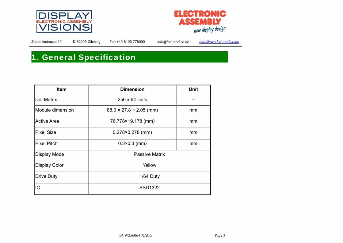
1. General Specification
Item Dimension Unit
Dot Matrix 256 x 64 Dots -
Module dimension 88.0 × 27.8 × 2.05 (mm) mm
Active Area 76.778×19.178 (mm) mm
Pixel Size 0.278×0.278 (mm) mm
Pixel Pitch 0.3×0.3 (mm) mm
Display Mode Passive Matrix
Display Color Yellow
Drive Duty 1/64 Duty
IC SSD1322
Zeppelinstrasse 19 D-82205 Gilching Fon +49-8105-778090 [email protected] http://www.lcd-module.de
EA W256064-XALG Page 4
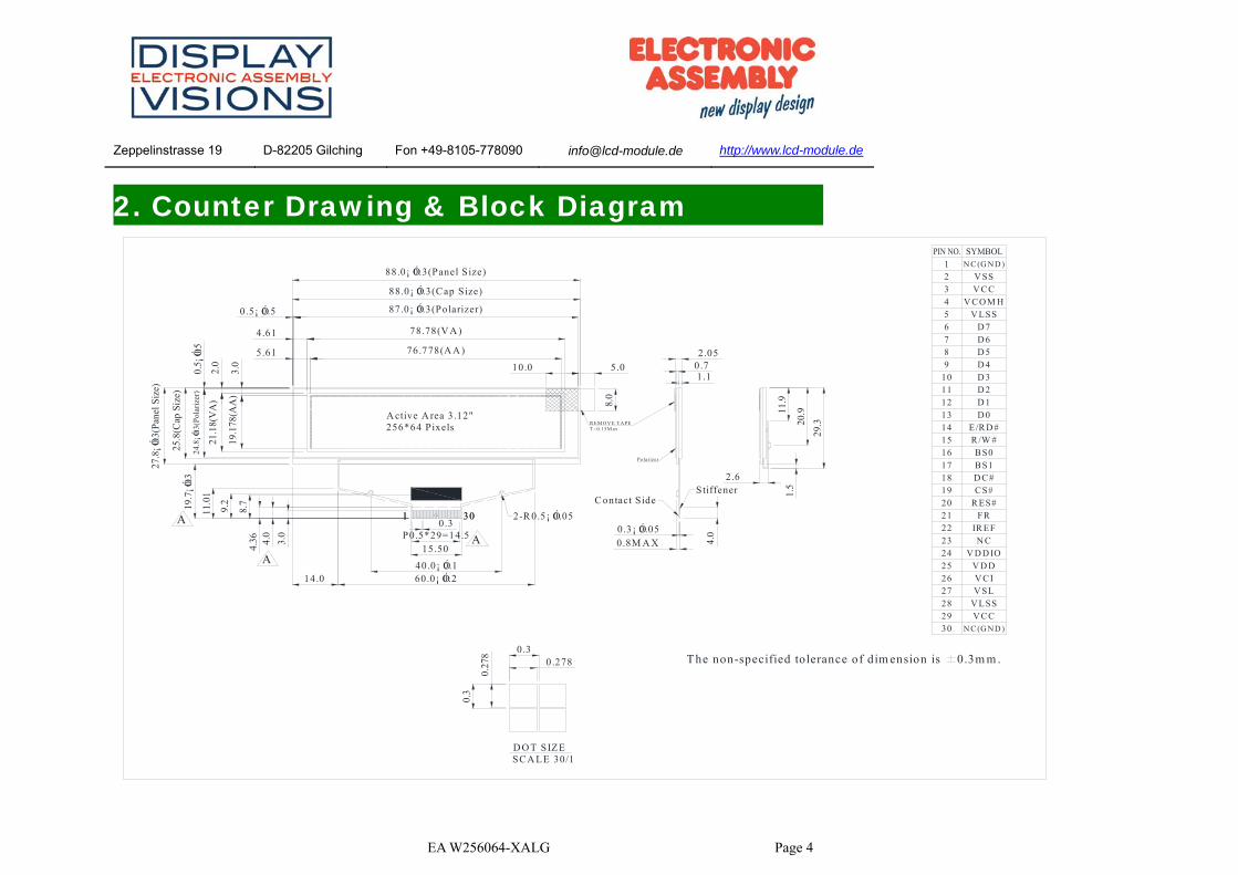
2. Counter Drawing & Block Diagram
E/R D #
D O T SIZESCA LE 30/1
V SSV CC
V C O M HV LSS
23
56
4
D 6D 5D 4D 3
98
1011
7D 7
1 N C (G N D )
D 1D 013
14
12D 2
The non-specified tolerance of dim ension is 0.3m m .0.2780.3
0.27
8
0.3
1516
1819
17
2021222324
2627
25
282930
R/W #
BS1D C#CS#
R ES#
BS0
IR EFN C
FR
V D D IOV D D
V SLV LSS
V CI
V CCN C (G N D )
1 30
19.7
¡Ó0.3
11.0
1
9.2
8.7
4.36 3.
0
14.0 60.0¡ Ó0.240.0¡ Ó0.1
P0.5*29=14.50.3
2-R 0.5¡ Ó0.051 30
SSD1322
88.0¡ Ó0.3(Panel Size)
88.0¡ Ó0.3(Cap Size)
0.5¡ Ó0.5 87.0¡ Ó0.3(Polarizer)
4.61 78.78(V A )
5.61 76.778(A A )
5.010.0
8.0
27.8
¡Ó0.
3(P
anel
Siz
e)
25.8
(Cap
Siz
e)
0.5¡
Ó0.5
24.8
¡Ó0.3
(Pol
ariz
er)
2.0
21.1
8(V
A)
3.0
19.1
78(A
A)
A ctive A rea 3.12"256*64 Pixels
2.05
0.3¡ Ó0.05
C ontact SideStiffener
4.0
11.9
20.9
29.3
1.5
2 .6
0.8M A X
R EM O V E TAPET =0.15M ax
Polarizer
0 .71.1
NC
D7
VCC
VL
SS
VCO
MH
VSS
NC
D3
D4
D5
D6
D2
E BS0
BS1
R/W
#
D1
D0
RE
S#
IREF
FRCS#
DC#
VL
SS
VSL
VCI
VD
D
VD
DIO
NC
VCC
4.0
15.50A
A
A
Zeppelinstrasse 19 D-82205 Gilching Fon +49-8105-778090 [email protected] http://www.lcd-module.de
EA W256064-XALG Page 5
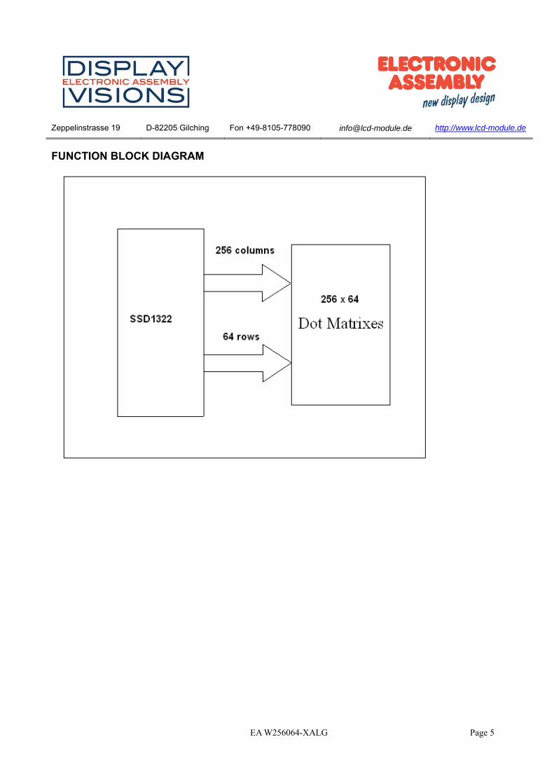
FUNCTION BLOCK DIAGRAM
Zeppelinstrasse 19 D-82205 Gilching Fon +49-8105-778090 [email protected] http://www.lcd-module.de
EA W256064-XALG Page 6
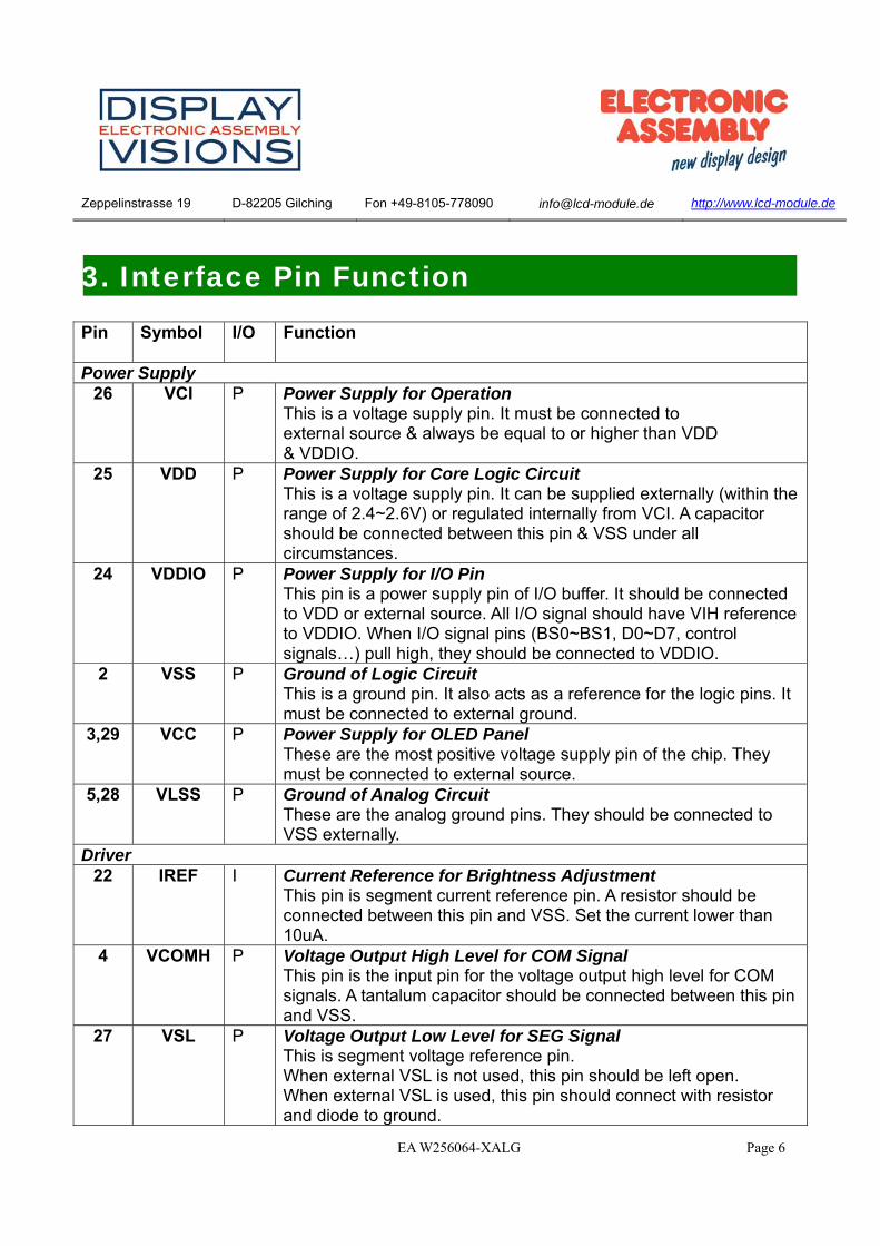
3. Interface Pin Function
Pin
Symbol I/O Function
Power Supply 26 VCI P Power Supply for Operation
This is a voltage supply pin. It must be connected to external source & always be equal to or higher than VDD & VDDIO.
25 VDD P Power Supply for Core Logic Circuit This is a voltage supply pin. It can be supplied externally (within the range of 2.4~2.6V) or regulated internally from VCI. A capacitor should be connected between this pin & VSS under all circumstances.
24 VDDIO P Power Supply for I/O Pin This pin is a power supply pin of I/O buffer. It should be connected to VDD or external source. All I/O signal should have VIH reference to VDDIO. When I/O signal pins (BS0~BS1, D0~D7, control signals…) pull high, they should be connected to VDDIO.
2 VSS P Ground of Logic Circuit This is a ground pin. It also acts as a reference for the logic pins. It must be connected to external ground.
3,29 VCC P Power Supply for OLED Panel These are the most positive voltage supply pin of the chip. They must be connected to external source.
5,28 VLSS P Ground of Analog Circuit These are the analog ground pins. They should be connected to VSS externally.
Driver 22 IREF I Current Reference for Brightness Adjustment
This pin is segment current reference pin. A resistor should be connected between this pin and VSS. Set the current lower than 10uA.
4 VCOMH P Voltage Output High Level for COM Signal This pin is the input pin for the voltage output high level for COM signals. A tantalum capacitor should be connected between this pin and VSS.
27 VSL P Voltage Output Low Level for SEG Signal This is segment voltage reference pin. When external VSL is not used, this pin should be left open. When external VSL is used, this pin should connect with resistor and diode to ground.
Zeppelinstrasse 19 D-82205 Gilching Fon +49-8105-778090 [email protected] http://www.lcd-module.de
EA W256064-XALG Page 7
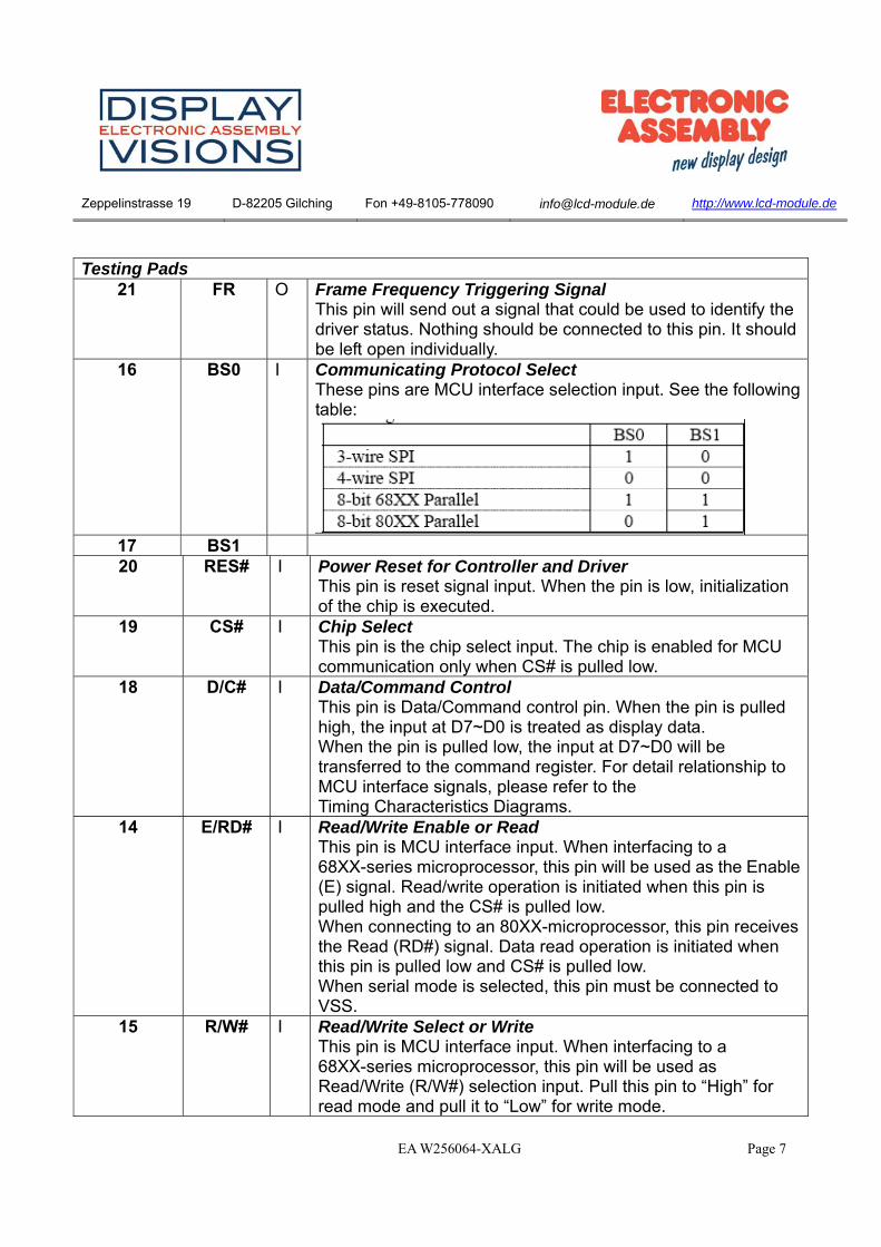
Testing Pads
21 FR O Frame Frequency Triggering Signal This pin will send out a signal that could be used to identify the driver status. Nothing should be connected to this pin. It should be left open individually.
16 BS0 I Communicating Protocol Select These pins are MCU interface selection input. See the following table:
17 BS1 20 RES# I Power Reset for Controller and Driver
This pin is reset signal input. When the pin is low, initialization of the chip is executed.
19 CS# I Chip Select This pin is the chip select input. The chip is enabled for MCU communication only when CS# is pulled low.
18 D/C# I Data/Command Control This pin is Data/Command control pin. When the pin is pulled high, the input at D7~D0 is treated as display data. When the pin is pulled low, the input at D7~D0 will be transferred to the command register. For detail relationship to MCU interface signals, please refer to the Timing Characteristics Diagrams.
14 E/RD# I Read/Write Enable or Read This pin is MCU interface input. When interfacing to a 68XX-series microprocessor, this pin will be used as the Enable (E) signal. Read/write operation is initiated when this pin is pulled high and the CS# is pulled low. When connecting to an 80XX-microprocessor, this pin receives the Read (RD#) signal. Data read operation is initiated when this pin is pulled low and CS# is pulled low. When serial mode is selected, this pin must be connected to VSS.
15 R/W# I Read/Write Select or Write This pin is MCU interface input. When interfacing to a 68XX-series microprocessor, this pin will be used as Read/Write (R/W#) selection input. Pull this pin to “High” for read mode and pull it to “Low” for write mode.

Zeppelinstrasse 19 D-82205 Gilching Fon +49-8105-778090 [email protected] http://www.lcd-module.de
EA W256064-XALG Page 8
When 80XX interface mode is selected, this pin will be the Write (WR#) input. Data write operation is initiated when this pin is pulled low and the CS# is pulled low. When serial mode is selected, this pin must be connected to VSS.
6~13 D7~D0 I/O Host Data Input/Output Bus These pins are 8-bit bi-directional data bus to be connected to the microprocessor’s data bus. When serial mode is selected, D1 will be the serial data input SDIN and D0 will be the serial clock input SCLK. Unused pins must be connected to VSS except for D2 in serial mode.
Reserve 23 N.C. - Reserved Pin
The N.C. pin between function pins are reserved for compatible and flexible design.
1,30 N.C. (GND)
- Reserved Pin (Supporting Pin) The supporting pins can reduce the influences from stresses on the function pins. These pins must be connected to external ground.
Zeppelinstrasse 19 D-82205 Gilching Fon +49-8105-778090 [email protected] http://www.lcd-module.de
EA W256064-XALG Page 9
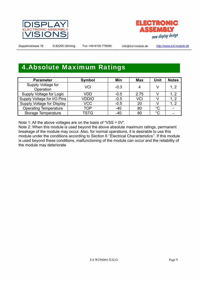
4.Absolute Maximum Ratings
Parameter Symbol Min Max Unit Notes Supply Voltage for
Operation VCI -0.3 4 V 1, 2
Supply Voltage for Logic VDD -0.5 2.75 V 1, 2 Supply Voltage for I/O Pins VDDIO -0.5 VCI V 1, 2 Supply Voltage for Display VCC -0.5 20 V 1, 2
Operating Temperature TOP -40 80 °C - Storage Temperature TSTG -40 80 °C -
Note 1: All the above voltages are on the basis of “VSS = 0V”. Note 2: When this module is used beyond the above absolute maximum ratings, permanent breakage of the module may occur. Also, for normal operations, it is desirable to use this module under the conditions according to Section 6 ‘’Electrical Characteristics’’. If this module is used beyond these conditions, malfunctioning of the module can occur and the reliability of the module may deteriorate
Zeppelinstrasse 19 D-82205 Gilching Fon +49-8105-778090 [email protected] http://www.lcd-module.de
EA W256064-XALG Page 10
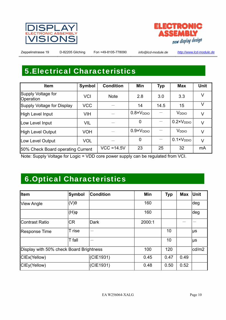
5.Electrical Characteristics
Item Symbol Condition Min Typ Max Unit
Supply Voltage for Operation
VCI Note 2.8 3.0 3.3 V
Supply Voltage for Display VCC - 14 14.5 15 V
High Level Input VIH - 0.8×VDDIO - VDDIO V
Low Level Input VIL - 0 - 0.2×VDDIO V
High Level Output VOH - 0.9×VDDIO - VDDIO V
Low Level Output VOL - 0 - 0.1×VDDIO V
50% Check Board operating Current VCC =14.5V 23 25 32 mA
Note: Supply Voltage for Logic = VDD core power supply can be regulated from VCI.
6.Optical Characteristics
Item Symbol Condition Min Typ Max Unit
View Angle (V)θ 160 deg
(H)φ 160 deg
Contrast Ratio CR Dark 2000:1 - -
Response Time T rise - 10 μs
T fall - 10 μs
Display with 50% check Board Brightness 100 120 cd/m2
CIEx(Yellow) (CIE1931) 0.45 0.47 0.49
CIEy(Yellow) (CIE1931) 0.48 0.50 0.52
Zeppelinstrasse 19 D-82205 Gilching Fon +49-8105-778090 [email protected] http://www.lcd-module.de
EA W256064-XALG Page 11
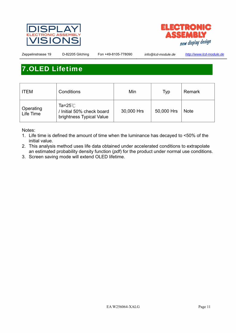
7.OLED Lifetime
ITEM Conditions Min Typ Remark
Operating Life Time
Ta=25℃ / Initial 50% check board brightness Typical Value
30,000 Hrs 50,000 Hrs Note
Notes: 1. Life time is defined the amount of time when the luminance has decayed to <50% of the
initial value. 2. This analysis method uses life data obtained under accelerated conditions to extrapolate
an estimated probability density function (pdf) for the product under normal use conditions. 3. Screen saving mode will extend OLED lifetime.
Zeppelinstrasse 19 D-82205 Gilching Fon +49-8105-778090 [email protected] http://www.lcd-module.de
EA W256064-XALG Page 12
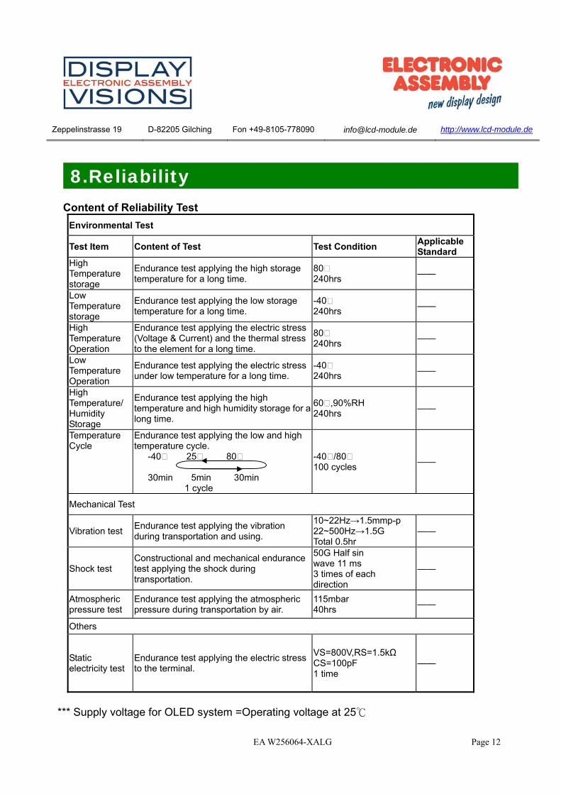
8.Reliability
Content of Reliability Test
Environmental Test
Test Item Content of Test Test Condition Applicable Standard
High Temperature storage
Endurance test applying the high storage temperature for a long time.
80 240hrs
——
Low Temperature storage
Endurance test applying the low storage temperature for a long time.
-40 240hrs
——
High Temperature Operation
Endurance test applying the electric stress (Voltage & Current) and the thermal stress to the element for a long time.
80 240hrs
——
Low Temperature Operation
Endurance test applying the electric stress under low temperature for a long time.
-40 240hrs
——
High Temperature/ Humidity Storage
Endurance test applying the high temperature and high humidity storage for a long time.
60 ,90%RH 240hrs
——
Temperature Cycle
Endurance test applying the low and high temperature cycle. -40 25 80 30min 5min 30min 1 cycle
-40 /80 100 cycles
——
Mechanical Test
Vibration test Endurance test applying the vibration during transportation and using.
10~22Hz→1.5mmp-p 22~500Hz→1.5G Total 0.5hr
——
Shock test Constructional and mechanical endurance test applying the shock during transportation.
50G Half sin wave 11 ms 3 times of each direction
——
Atmospheric pressure test
Endurance test applying the atmospheric pressure during transportation by air.
115mbar 40hrs
——
Others
Static electricity test
Endurance test applying the electric stress to the terminal.
VS=800V,RS=1.5kΩ CS=100pF 1 time
——
*** Supply voltage for OLED system =Operating voltage at 25℃
Zeppelinstrasse 19 D-82205 Gilching Fon +49-8105-778090 [email protected] http://www.lcd-module.de
EA W256064-XALG Page 13
Test and measurement conditions 1. All measurements shall not be started until the specimens attain to temperature stability.
After the completion of the described reliability test, the samples were left at room temperature for 2 hrs prior to conducting the failure test at 23±5°C; 55±15% RH.
2. All-pixels-on is used as operation test pattern. 3. The degradation of Polarizer are ignored for High Temperature storage, High Temperature/
Humidity Storage, Temperature Cycle Evaluation criteria 1. The function test is OK. 2. No observable defects. 3. Luminance: > 50% of initial value. 4. Current consumption: within ± 50% of initial value. APPENDIX: RESIDUE IMAGE Because the pixels are lighted in different time, the luminance of active pixels may reduce or differ from inactive pixels. Therefore, the residue image will occur. To avoid the residue image, every pixel needs to be lighted up uniformly.

Zeppelinstrasse 19 D-82205 Gilching Fon +49-8105-778090 [email protected] http://www.lcd-module.de
EA W256064-XALG Page 14
9.Inspection specification NO Item Criterion AQL01 Electrical
Testing 1.1 Missing vertical, horizontal segment, segment contrast defect. 1.2 Missing character , dot or icon. 1.3 Display malfunction. 1.4 No function or no display. 1.5 Current consumption exceeds product specifications. 1.6 OLED viewing angle defect. 1.7 Mixed product types. 1.8 Contrast defect.
0.65
02 Black or white spots on OLED (display only)
2.1 White and black spots on display 0.25mm, no more than three white or black spots present. 2.2 Densely spaced: No more than two spots or lines within 3mm.
2.5
03 OLED black spots, white spots, contamination (non-display)
3.1 Round type : As following drawing Φ=( x + y ) / 2
2.5
3.2 Line type : (As following drawing)
2.5
04 Polarizer bubbles
If bubbles are visible, judge using black spot specifications, not easy to find, must check in specify direction.
2.5
SIZE Acceptable Q TY
Φ≦0.10 Accept no dense
0.10<
Φ≦0.20 2
0.20<
Φ≦0.25 1
0 25<Φ 0
Length Width Acceptable Q TY --- W≦0.02 Accept no dense L≦3.0 0.02<W≦0.03 2 L≦2.5 0.03<W≦0.05 --- 0.05<W As round type
Size Φ Acceptable Q TY Φ≦0.20 Accept no dense 0.20<Φ≦0.50 3 0.50<Φ≦1.00 2 1.00<Φ 0 Total Q TY 3
Zeppelinstrasse 19 D-82205 Gilching Fon +49-8105-778090 [email protected] http://www.lcd-module.de
EA W256064-XALG Page 15
NO Item Criterion AQL05 Scratches Follow NO.3 OLED black spots, white spots, contamination
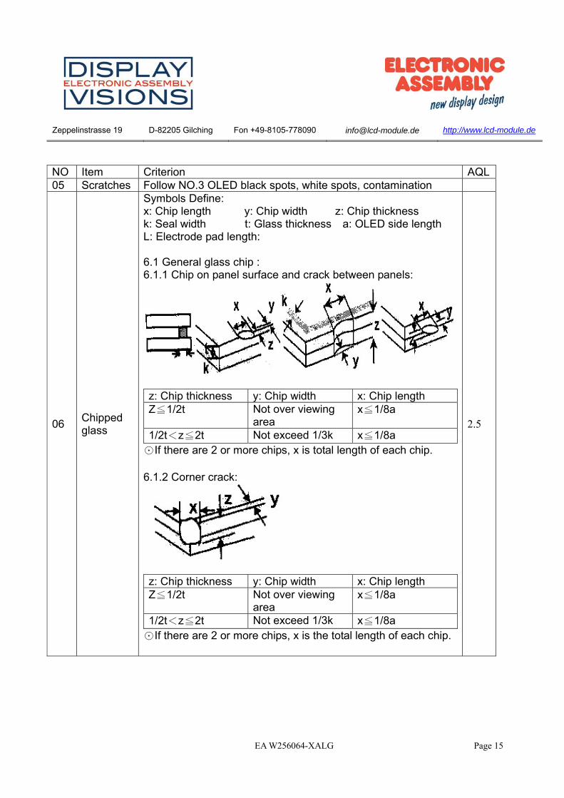
06 Chipped glass
Symbols Define: x: Chip length y: Chip width z: Chip thickness k: Seal width t: Glass thickness a: OLED side length L: Electrode pad length: 6.1 General glass chip : 6.1.1 Chip on panel surface and crack between panels:
z: Chip thickness y: Chip width x: Chip length Z≦1/2t Not over viewing
area x≦1/8a
1/2t<z≦2t Not exceed 1/3k x≦1/8a
☉If there are 2 or more chips, x is total length of each chip. 6.1.2 Corner crack:
z: Chip thickness y: Chip width x: Chip length Z≦1/2t Not over viewing
area x≦1/8a
1/2t<z≦2t Not exceed 1/3k x≦1/8a
☉If there are 2 or more chips, x is the total length of each chip.
2.5
Zeppelinstrasse 19 D-82205 Gilching Fon +49-8105-778090 [email protected] http://www.lcd-module.de
EA W256064-XALG Page 16
NO Item Criterion AQL
06 Glass crack
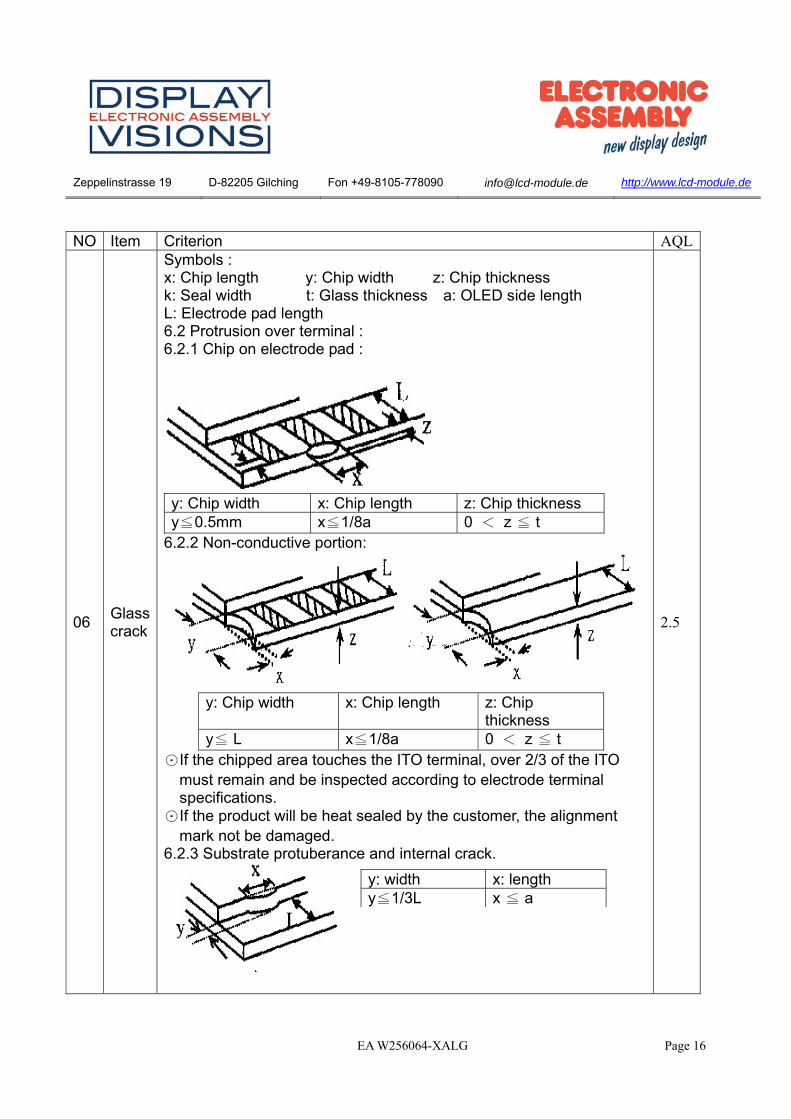
Symbols : x: Chip length y: Chip width z: Chip thickness k: Seal width t: Glass thickness a: OLED side length L: Electrode pad length 6.2 Protrusion over terminal : 6.2.1 Chip on electrode pad :
y: Chip width x: Chip length z: Chip thickness y≦0.5mm x≦1/8a 0 < z ≦ t
6.2.2 Non-conductive portion:
y: Chip width x: Chip length z: Chip
thickness y≦ L x≦1/8a 0 < z ≦ t
☉If the chipped area touches the ITO terminal, over 2/3 of the ITO must remain and be inspected according to electrode terminal specifications.
☉If the product will be heat sealed by the customer, the alignment mark not be damaged.
6.2.3 Substrate protuberance and internal crack.
2.5
y: width x: length y≦1/3L x ≦ a
Zeppelinstrasse 19 D-82205 Gilching Fon +49-8105-778090 [email protected] http://www.lcd-module.de
EA W256064-XALG Page 17
NO Item Criterion AQL
07 Cracked glass
The OLED with extensive crack is not acceptable. 2.5
08 Backlight elements
8.1 Illumination source flickers when lit. 8.2 Spots or scratched that appear when lit must be judged.
Using OLED spot, lines and contamination standards. 8.3 Backlight doesn’t light or color wrong.
0.65 2.5 0.65
09 Bezel
9.1 Bezel may not have rust, be deformed or have
fingerprints, stains or other contamination. 9.2 Bezel must comply with job specifications.
2.5 0.65
10 PCB、COB
10.1 COB seal may not have pinholes larger than 0.2mm or
contamination. 10.2 COB seal surface may not have pinholes through to the
IC. 10.3 The height of the COB should not exceed the height
indicated in the assembly diagram. 10.4 There may not be more than 2mm of sealant outside the
seal area on the PCB. And there should be no more than three places.
10.5 No oxidation or contamination PCB terminals. 10.6 Parts on PCB must be the same as on the production
characteristic chart. There should be no wrong parts, missing parts or excess parts.
10.7 The jumper on the PCB should conform to the product characteristic chart.
10.8 If solder gets on bezel tab pads, OLED pad, zebra pad or screw hold pad, make sure it is smoothed down.
2.5 2.5 0.65 2.5 2.5 0.65 0.65 2.5
11 Soldering
11.1 No un-melted solder paste may be present on the PCB. 11.2 No cold solder joints, missing solder connections,
oxidation or icicle. 11.3 No residue or solder balls on PCB. 11.4 No short circuits in components on PCB.
2.5 2.5 2.5 0.65
Zeppelinstrasse 19 D-82205 Gilching Fon +49-8105-778090 [email protected] http://www.lcd-module.de
EA W256064-XALG Page 18
NO Item Criterion AQL
12 General appearance
12.1 No oxidation, contamination, curves or, bends on
interface Pin (OLB) of TCP. 12.2 No cracks on interface pin (OLB) of TCP. 12.3 No contamination, solder residue or solder balls on
product. 12.4 The IC on the TCP may not be damaged, circuits. 12.5 The uppermost edge of the protective strip on the
interface pin must be present or look as if it cause the interface pin to sever.
12.6 The residual rosin or tin oil of soldering (component or chip component) is not burned into brown or black color.
12.7 Sealant on top of the ITO circuit has not hardened. 12.8 Pin type must match type in specification sheet. 12.9 OLED pin loose or missing pins. 12.10 Product packaging must the same as specified on
packaging specification sheet. 12.11 Product dimension and structure must conform to
product specification sheet.
2.5 0.65 2.5 2.5 2.5 2.5 2.5 0.65 0.65 0.65 0.65
Zeppelinstrasse 19 D-82205 Gilching Fon +49-8105-778090 [email protected] http://www.lcd-module.de
EA W256064-XALG Page 19
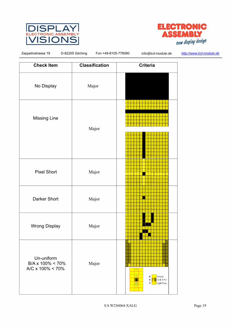
Check Item Classification Criteria
No Display
Major
Missing Line
Major
Pixel Short
Major
Darker Short
Major
Wrong Display
Major
Un-uniform B/A x 100% < 70%
A/C x 100% < 70%
Major
Zeppelinstrasse 19 D-82205 Gilching Fon +49-8105-778090 [email protected] http://www.lcd-module.de
EA W256064-XALG Page 20
10.Precautions in use of OLED Modules Modules
(1)Avoid applying excessive shocks to module or making any alterations or modifications to it. (2)Don’t make extra holes on the printed circuit board, modify its shape or change the
components of OLED display module. (3)Don’t disassemble the OLED display module. (4)Don’t operate it above the absolute maximum rating. (5)Don’t drop, bend or twist OLED display module. (6)Soldering: only to the I/O terminals. (7)Storage: please storage in anti-static electricity container and clean environment. (8)It's pretty common to use "Screen Saver" to extend the lifetime and Don't use fix information
for long time in real application. (9)Don't use fixed information in OLED panel for long time, that will extend "screen burn" effect
time.. (10)ELECTRONIC ASSEMBLY has the right to change the passive components, including
R2and R3 adjust resistors. (Resistors, capacitors and other passive components will have different appearance and color caused by the different supplier.)
(11) ELECTRONIC ASSEMBLY have the right to change the PCB Rev. (In order to satisfy the supplying stability, management optimization and the best product performance...etc, under the premise of not affecting the electrical characteristics and external dimensions, ELECTRONIC ASSEMBLY have the right to modify the version.)
11.1. Handling Precautions (1) Since the display panel is being made of glass, do not apply mechanical impacts such us
dropping from a high position. (2) If the display panel is broken by some accident and the internal organic substance leaks out,
be careful not to inhale nor lick the organic substance. (3) If pressure is applied to the display surface or its neighborhood of the OLED display module,
the cell structure may be damaged and be careful not to apply pressure to these sections. (4) The polarizer covering the surface of the OLED display module is soft and easily scratched.
Please be careful when handling the OLED display module. (5) When the surface of the polarizer of the OLED display module has soil, clean the surface. It
takes advantage of by using following adhesion tape. * Scotch Mending Tape No. 810 or an equivalent Never try to breathe upon the soiled surface nor wipe the surface using cloth containing
solvent such as ethyl alcohol, since the surface of the polarizer will become cloudy. Also, pay attention that the following liquid and solvent may spoil the polarizer: * Water * Ketone * Aromatic Solvents
(6) Hold OLED display module very carefully when placing OLED display module into the

Zeppelinstrasse 19 D-82205 Gilching Fon +49-8105-778090 [email protected] http://www.lcd-module.de
EA W256064-XALG Page 21
System housing. Do not apply excessive stress or pressure to OLED display module. And, do not over bend the film with electrode pattern layouts. These stresses will influence the display performance. Also, secure sufficient rigidity for the outer cases.
(7) Do not apply stress to the LSI chips and the surrounding molded sections. (8) Do not disassemble nor modify the OLED display module. (9) Do not apply input signals while the logic power is off. (10) Pay sufficient attention to the working environments when handing OLED display modules to prevent occurrence of element breakage accidents by static electricity. * Be sure to make human body grounding when handling OLED display modules. * Be sure to ground tools to use or assembly such as soldering irons. * To suppress generation of static electricity, avoid carrying out assembly work under dry
environments. * Protective film is being applied to the surface of the display panel of the OLED display module. Be careful since static electricity may be generated when exfoliating the protective film. (11) Protection film is being applied to the surface of the display panel and removes the protection film before assembling it. At this time, if the OLED display module has been stored for a long period of time, residue adhesive material of the protection film may remain on the surface of the display panel after removed of the film. In such case, remove the residue material by the method introduced in the above Section 5. (12) If electric current is applied when the OLED display module is being dewed or when it is placed under high humidity environments, the electrodes may be corroded and be careful to avoid the above. 11.2. Storage Precautions (1) When storing OLED display modules, put them in static electricity preventive bags avoiding exposure to direct sun light nor to lights of fluorescent lamps. and, also, avoiding high temperature and high humidity environment or low temperature (less than 0°C) environments. (We recommend you to store these modules in the packaged state when they were shipped from ELECTRONIC ASSEMBLY Technology Inc. At that time, be careful not to let water drops adhere to the packages or bags nor let dewing
occur with them. (2) If electric current is applied when water drops are adhering to the surface of the OLED
Zeppelinstrasse 19 D-82205 Gilching Fon +49-8105-778090 [email protected] http://www.lcd-module.de
EA W256064-XALG Page 22
display module, when the OLED display module is being dewed or when it is placed under high humidity environments, the electrodes may be corroded and be careful about the above. 11.3. Designing Precautions (1) The absolute maximum ratings are the ratings which cannot be exceeded for OLED display module, and if these values are exceeded, panel damage may be happen. (2) To prevent occurrence of malfunctioning by noise, pay attention to satisfy the VIL and VIH specifications and, at the same time, to make the signal line cable as short as possible. (3) We recommend you to install excess current preventive unit (fuses, etc.) to the power circuit (VDD). (Recommend value: 0.5A) (4) Pay sufficient attention to avoid occurrence of mutual noise interference with the neighboring devices. (5) As for EMI, take necessary measures on the equipment side basically. (6) When fastening the OLED display module, fasten the external plastic housing section. (7) If power supply to the OLED display module is forcibly shut down by such errors as taking out the main battery while the OLED display panel is in operation, we cannot guarantee the quality of this OLED display module. * Connection (contact) to any other potential than the above may lead to rupture of the IC.11.4. Precautions when disposing of the OLED display modules 1) Request the qualified companies to handle industrial wastes when disposing of the OLED
display modules. Or, when burning them, be sure to observe the environmental and hygienic laws and regulations.
11.5. Other Precautions (1) When an OLED display module is operated for a long of time with fixed pattern may remain
as an after image or slight contrast deviation may occur. Nonetheless, if the operation is interrupted and left unused for a while, normal state can be
restored. Also, there will be no problem in the reliability of the module. (2) To protect OLED display modules from performance drops by static electricity rapture, etc., do
not touch the following sections whenever possible while handling the OLED display modules. * Pins and electrodes * Pattern layouts such as the TCP & FPC (3) With this OLED display module, the OLED driver is being exposed. Generally speaking,
semiconductor elements change their characteristics when light is radiated according to the principle of the solar battery. Consequently, if this OLED driver is exposed to light, malfunctioning may occur.
* Design the product and installation method so that the OLED driver may be shielded from light in actual usage.
* Design the product and installation method so that the OLED driver may be shielded from light during the inspection processes.
(4) Although this OLED display module stores the operation state data by the commands and the indication data, when excessive external noise, etc. enters into the module, the internal status

Zeppelinstrasse 19 D-82205 Gilching Fon +49-8105-778090 [email protected] http://www.lcd-module.de
EA W256064-XALG Page 23
may be changed. It therefore is necessary to take appropriate measures to suppress noise generation or to protect from influences of noise on the system design.
(5) We recommend you to construct its software to make periodical refreshment of the operation statuses (re-setting of the commands and re-transference of the display data) to cope with catastrophic noise.
(6)Resistors, capacitors and other passive components will have different appearance and color caused by the different supplier.
(7)Our company will has the right to upgrade and modify the product function.
Zeppelinstrasse 19 D-82205 Gilching Fon +49-8105-778090 [email protected] http://www.lcd-module.de
EA W256064-XALG Page 24
11.Initialization example
/********************************************************************************* Global variables *********************************************************************************/ uint8_t buf[20]; //SPI command buffer uint8_t buffer[128]; //SPI data buffer const uint8_t lookupval[4] = {0x0,0xF,0xF0,0xFF}; //lookup table /********************************************************************************* Function name: command Description: send command via SPI *********************************************************************************/ void command(uint8_t command){ waitforemptybuffer(); //waits until SPI buffer is empty buf[0] = command; PORT5.PODR.BIT.B4 = 0; //set D/C# pin low R_RSPI0_Send(buf,1); //send buffer via SPI } /********************************************************************************* Function name: data Description: send data via SPI *********************************************************************************/ void data(uint8_t data){ waitforemptybuffer(); //waits until SPI buffer is empty buf[0] = data; PORT5.PODR.BIT.B4 = 1; //set D/C# pin high R_RSPI0_Send(buf,1); //send buffer via SPI } /********************************************************************************* Function name: initW256064 Description: Initialization of the display *********************************************************************************/ void initW256064 (void){
PORT5.PODR.BIT.B5 = 0; //Reset pin low ms_delay(100); //100ms delay PORT5.PODR.BIT.B5 = 1; //Reset pin high ms_delay(100); //100ms delay
command(0xFD); //set Command unlock data(0x12); command(0xAE); //set display off
Zeppelinstrasse 19 D-82205 Gilching Fon +49-8105-778090 [email protected] http://www.lcd-module.de
EA W256064-XALG Page 25
command(0xB3); //set display clock divide ratio... data(0x91); //...to 135 Frames/sec command(0xCA); //set multiplex ratio... data(0x3F); //...to 64‐1 command(0xA2); //set display offset data(0x00); //...to 0 command(0xA1); //start display start line data(0x00); //...to 0 command(0xA0); //set Re‐Map & Dual COM Line Mode data(0x14); data(0x11); command(0xB5); //disable IO intput data(0x00); command(0xAB); //function select data(0x01); command(0xB4); //enable VSL extern data(0xA0); data(0xFD); command(0xC1); //set contrast current data(0xFF); command(0xC7); //set master contrast current data(0x0F);
command(0xB8); //set gray scale table data(0x00); data(0x00); data(0x00); data(0x03); data(0x06); data(0x10); data(0x1D); data(0x2A); data(0x37); data(0x46); data(0x58); data(0x6A); data(0x7F); data(0x96); data(0xB4); command(0xB1); //set phase length data(0xE8);
Zeppelinstrasse 19 D-82205 Gilching Fon +49-8105-778090 [email protected] http://www.lcd-module.de
EA W256064-XALG Page 26
command(0xD1); //enhance driving scheme capability data(0x82); data(0x20); command(0xBB); //first pre charge voltage data(0x1F); command(0xB6); //second pre charge voltage data(0x08); command(0xBE); //VCOMH data(0x07); command(0xA9); //no partial mode command(0xA6); //set normal display mode ms_delay(1); //stabilize VDD command(0xAF); //display on ms_delay(200); //stabilize VDD } /********************************************************************************* Function name: initWindow Description: Initialization of the window in horizontal addressing mode *********************************************************************************/ void initWindow(uint8_t startcol, uint8_t stopcol, uint8_t startrow, uint8_t stoprow){
command(0x15); data(28+startcol); data(28+stopcol); command(0x75); data(startrow); data(stoprow); command(0x5C); ms_delay(50); }
Zeppelinstrasse 19 D-82205 Gilching Fon +49-8105-778090 [email protected] http://www.lcd-module.de
EA W256064-XALG Page 27
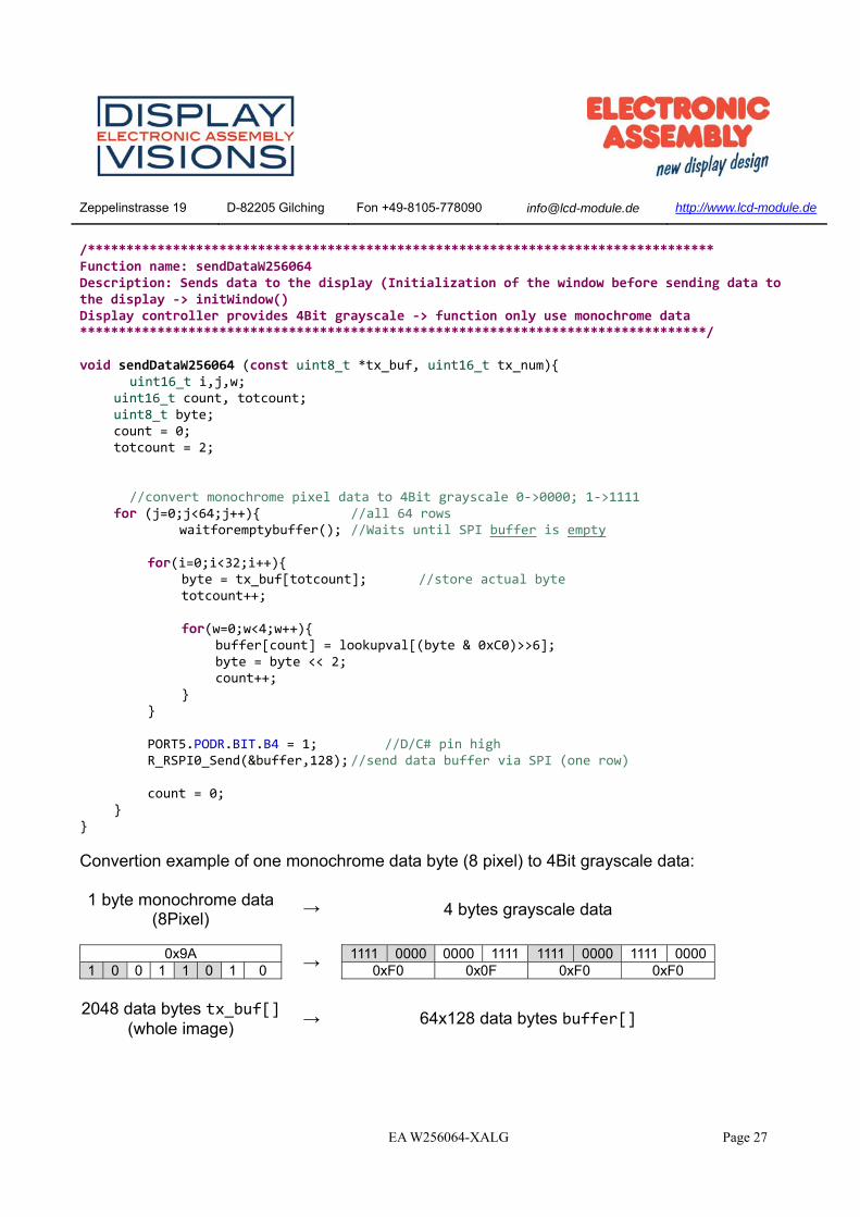
/********************************************************************************* Function name: sendDataW256064 Description: Sends data to the display (Initialization of the window before sending data to the display ‐> initWindow() Display controller provides 4Bit grayscale ‐> function only use monochrome data *********************************************************************************/ void sendDataW256064 (const uint8_t *tx_buf, uint16_t tx_num){
uint16_t i,j,w; uint16_t count, totcount; uint8_t byte; count = 0; totcount = 2;
//convert monochrome pixel data to 4Bit grayscale 0‐>0000; 1‐>1111 for (j=0;j<64;j++){ //all 64 rows
waitforemptybuffer(); //Waits until SPI buffer is empty
for(i=0;i<32;i++){ byte = tx_buf[totcount]; //store actual byte totcount++; for(w=0;w<4;w++){ buffer[count] = lookupval[(byte & 0xC0)>>6]; byte = byte << 2; count++; } } PORT5.PODR.BIT.B4 = 1; //D/C# pin high R_RSPI0_Send(&buffer,128); //send data buffer via SPI (one row) count = 0; } }
Convertion example of one monochrome data byte (8 pixel) to 4Bit grayscale data: 1 byte monochrome data
(8Pixel)
→
4 bytes grayscale data
0x9A 1 0 0 1 1 0 1 0
→ 1111 0000 0000 1111 1111 0000 1111 0000 0xF0 0x0F 0xF0 0xF0
2048 data bytes tx_buf[] (whole image)
→ 64x128 data bytes buffer[]
Zeppelinstrasse 19 D-82205 Gilching Fon +49-8105-778090 [email protected] http://www.lcd-module.de
EA W256064-XALG Page 28
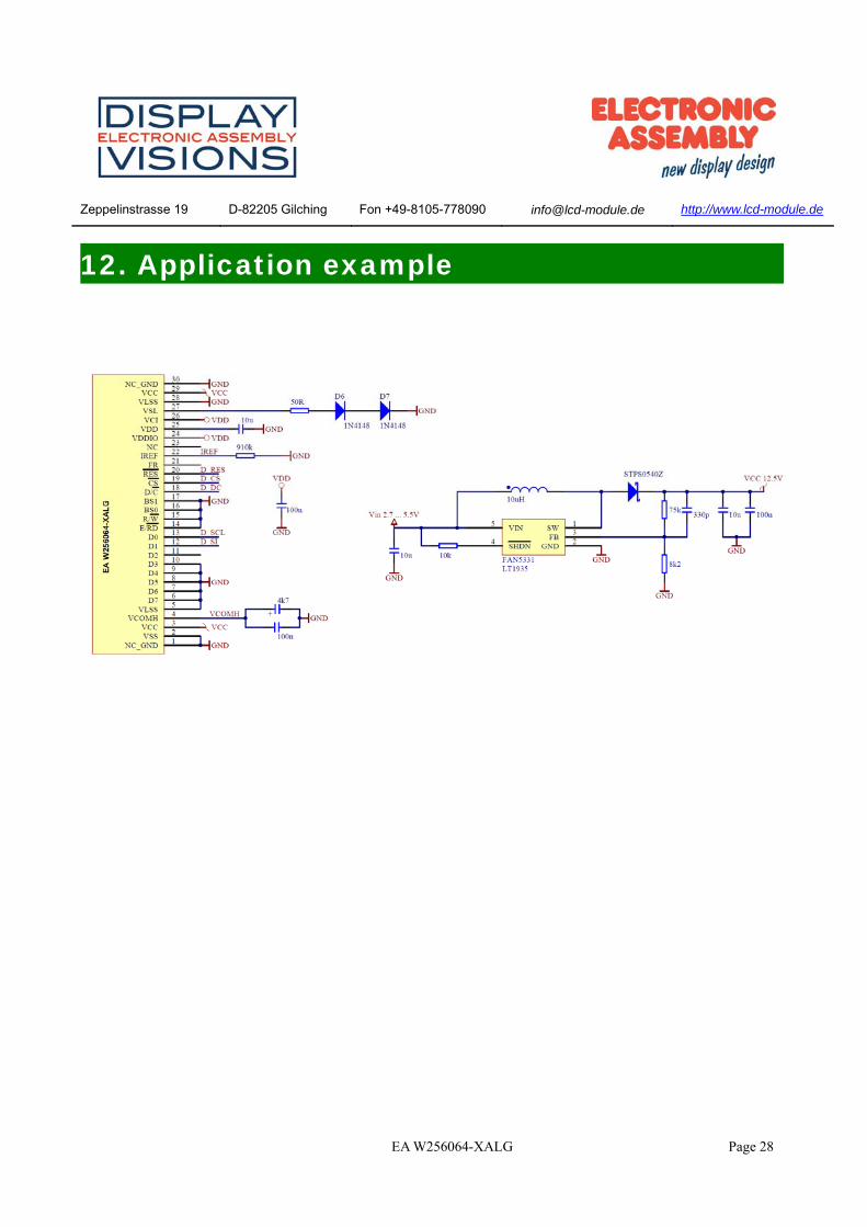
12. Application example