on-chip interconnect: the past, present, and futureasync.org.uk/noc2006/pdf/eby-friedman.pdfon-chip...
TRANSCRIPT
On-Chip Interconnect: The Past, Present, and Future
Professor Eby G. Friedman
Department of Electrical and Computer EngineeringUniversity of Rochester
URL: http://www.ece.rochester.edu/~friedman
Future Interconnects and Networks on Chip1st NoC Workshop – DATE ‘06
March 10, 2006

Agenda
• A historical perspective
• Where are we now ?
• Where are we going ?
• Conclusions

Agenda
⇒A historical perspective
• Where are we now ?
• Where are we going ?
• Conclusions
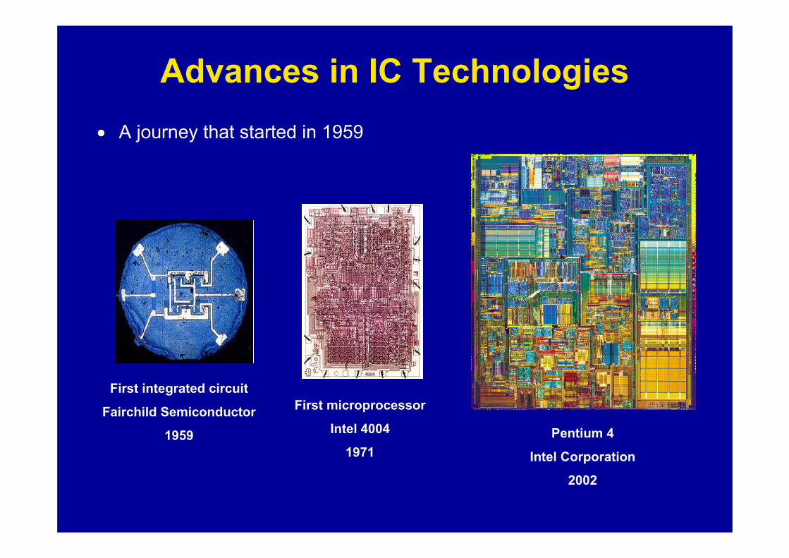
Advances in IC Technologies• A journey that started in 1959
First integrated circuit
Fairchild Semiconductor
1959
First microprocessor
Intel 4004
1971Pentium 4
Intel Corporation
2002
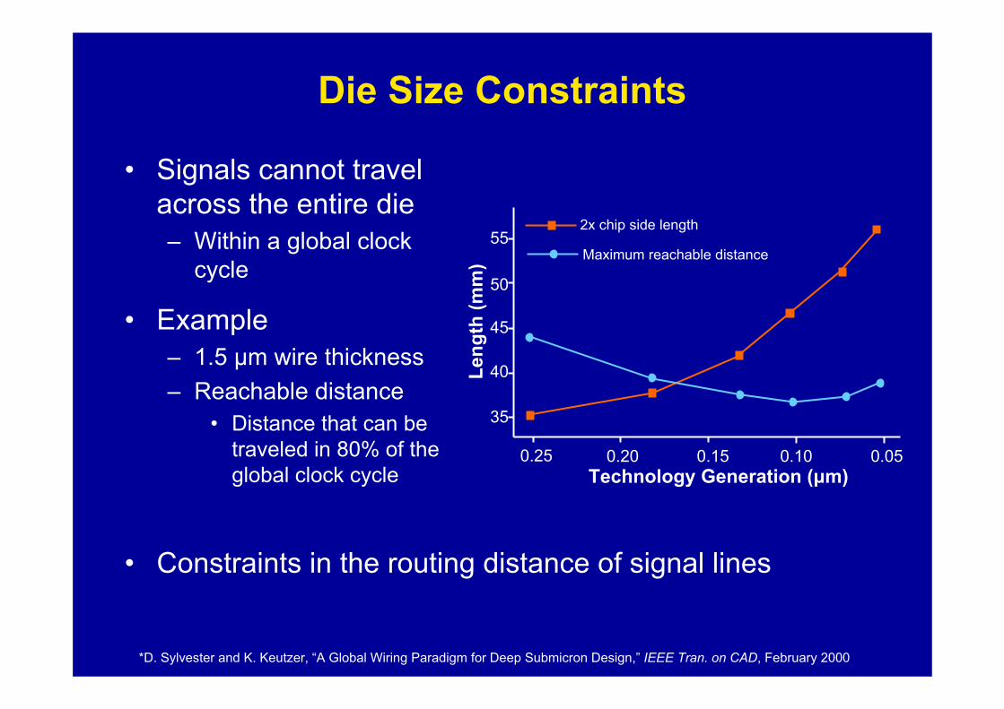
Die Size Constraints
• Signals cannot travel across the entire die– Within a global clock
cycle
35
40
45
50
55
0.25 0.20 0.15 0.10 0.05Le
ngth
(mm
)Technology Generation (μm)
2x chip side length
Maximum reachable distance
• Constraints in the routing distance of signal lines
*D. Sylvester and K. Keutzer, “A Global Wiring Paradigm for Deep Submicron Design,” IEEE Tran. on CAD, February 2000
• Example– 1.5 μm wire thickness– Reachable distance
• Distance that can be traveled in 80% of the global clock cycle

Two to three order of
magnitude delay difference
2001 International Technology Roadmap for Semiconductors
• Interconnect delay dominates gate delay– Global interconnect delay continuously increasing– Need multiple clock cycles to cross chip die– Limits the performance of microprocessors
Trends in Interconnect Delay
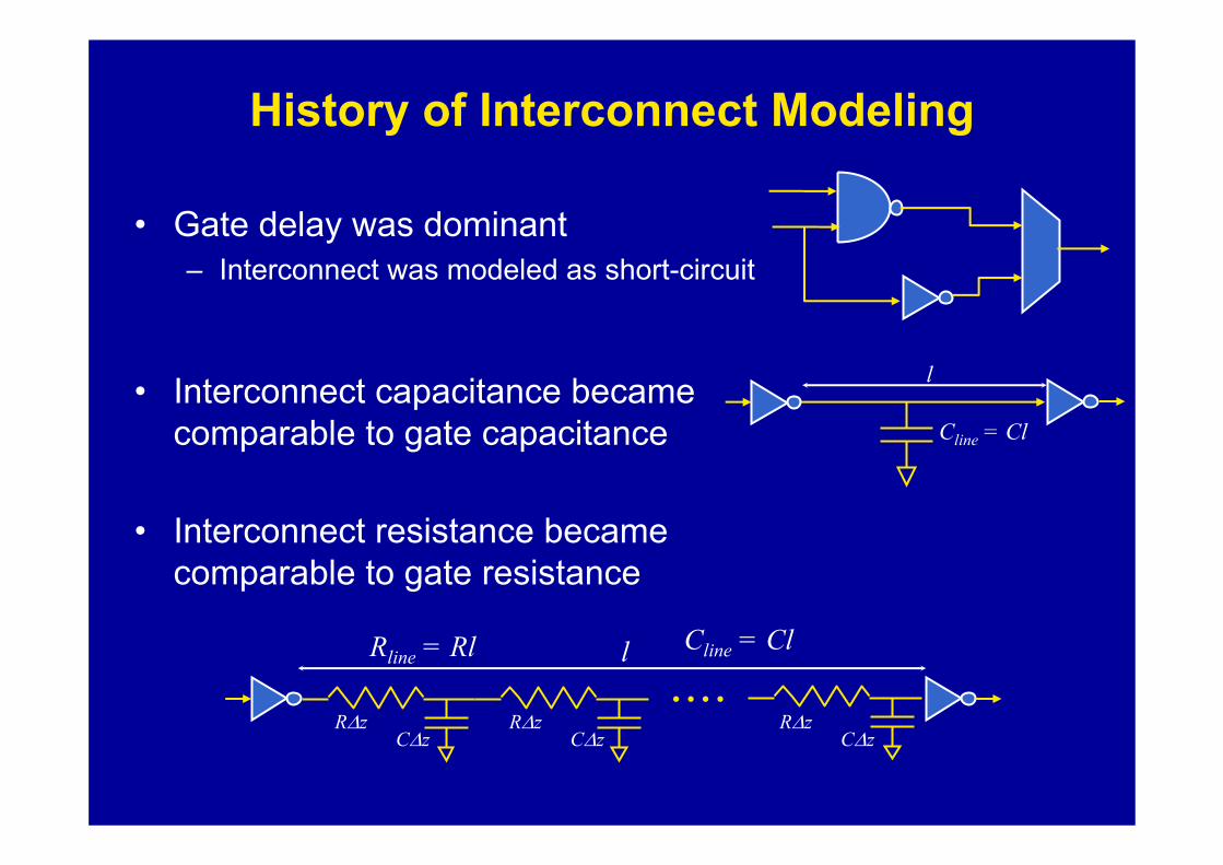
History of Interconnect Modeling
• Gate delay was dominant– Interconnect was modeled as short-circuit
• Interconnect capacitance became comparable to gate capacitance
l
Cline = Cl
• Interconnect resistance became comparable to gate resistance
• • • •
l
RΔzCΔz
RΔzCΔz
RΔzCΔz
Rline = Rl Cline = Cl
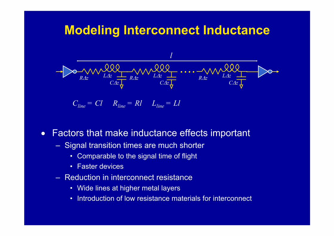
Modeling Interconnect Inductance
• Factors that make inductance effects important– Signal transition times are much shorter
• Comparable to the signal time of flight• Faster devices
– Reduction in interconnect resistance• Wide lines at higher metal layers• Introduction of low resistance materials for interconnect
• • • •
l
LΔzRΔzCΔz
Rline = RlCline = Cl Lline = Ll
LΔzRΔzCΔz
LΔzRΔzCΔz

• Significant inductance effects with technology scaling
Interconnect Models
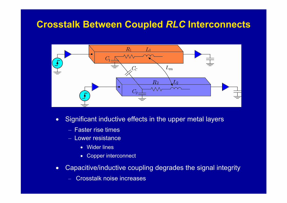
• Significant inductive effects in the upper metal layers– Faster rise times– Lower resistance
• Wider lines• Copper interconnect
• Capacitive/inductive coupling degrades the signal integrity– Crosstalk noise increases
Crosstalk Between Coupled RLC Interconnects

• Power distribution networks– Consume about 30% on-chip metal– IR, Ldi/dt noise– RLC resonances
• Clock distribution networks– Consume up to 70% of the total power– Clock skew, jitter
• Signals with multiple fan-out• Large global busses
• Interconnect networks have become increasingly complicated with greater integration
– Accurate and efficient models are required
0
1
2
3
4
5
6
7
8
9
10
11
Source
Interconnect Networks

Agenda
• A historical perspective
⇒Where are we now ?
• Where are we going ?
• Conclusions
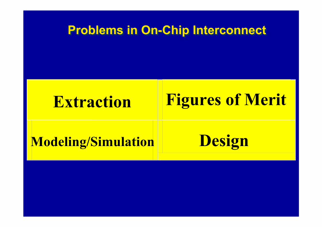
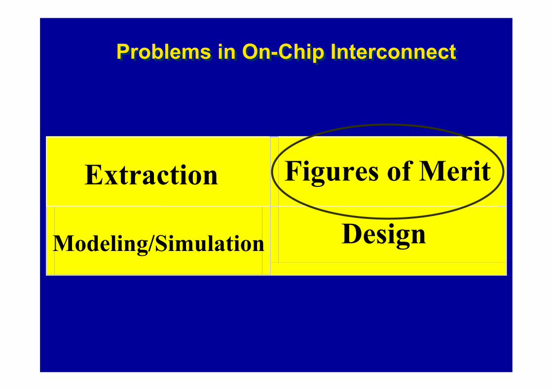
Problems in On-Chip InterconnectProblems in On-Chip Interconnect
Extraction Figures of Merit
Modeling/Simulation Design
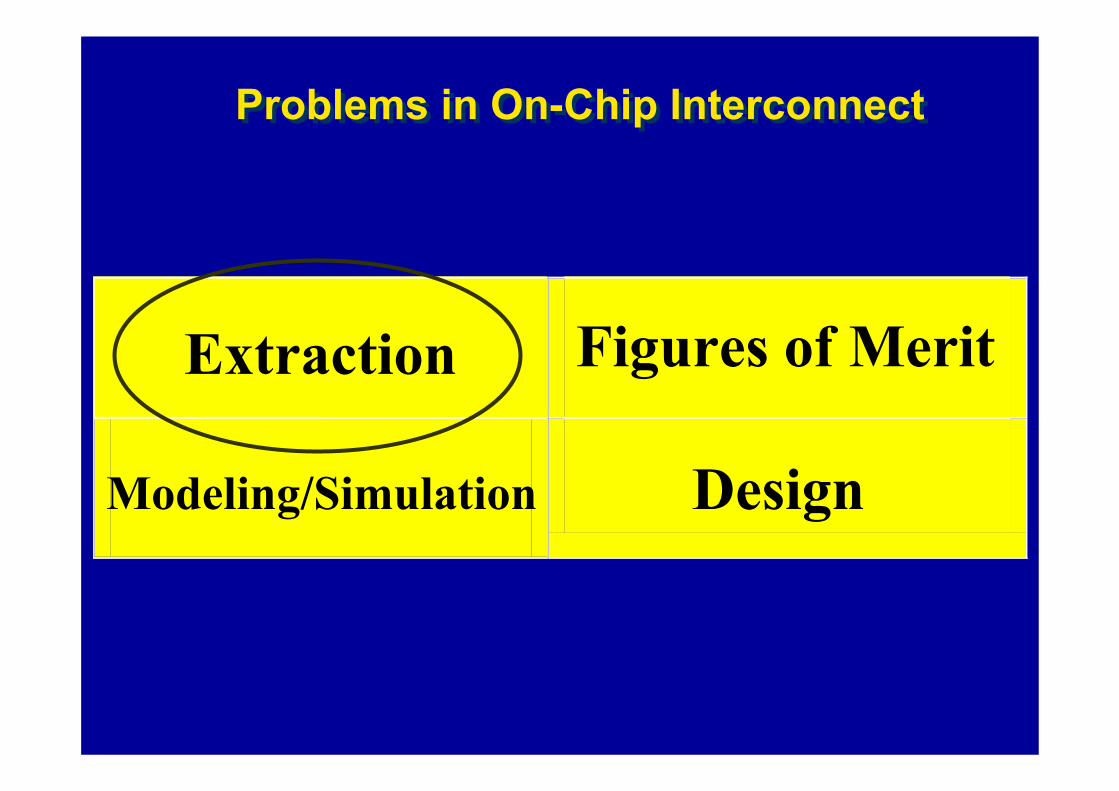
Problems in On-Chip InterconnectProblems in On-Chip Interconnect
Extraction Figures of Merit
Modeling/Simulation Design

Dependence of Impedance on Frequency:Multi-path Current Redistribution
• In a circuit with multiple current paths the distribution of the current flow is frequency dependent
– Low frequency — determined by the resistance of the paths– High frequency — determined by the inductance of the paths
• This effect is the primary source of inductance variation with frequency in integrated circuits
I0
I1
I2
Low ƒ, R >> jωL
Forward current
Return 1, low L1, high R1
Return 2, high L2, low R2
21
201 RR
RII+
≈21
102 RR
RII+
≈21
201 LL
LII+
≈21
102 LL
LII+
≈
I0
I1
I2
Forward current
Return 1, low L1, high R1
High ƒ, R << jωL
Return 2, high L2, low R2
* A. V. Mezhiba and E. G. Friedman, “Impedance Characteristics of Power Distribution Grids in Nanoscale Integrated Circuits," IEEE Transactions on Very Large Scale Integration (VLSI) Systems, Vol. 12, No. 11, pp. 1148-1155, November 2004.
Problems in On-Chip InterconnectProblems in On-Chip Interconnect
Extraction Figures of Merit
Modeling/Simulation Design
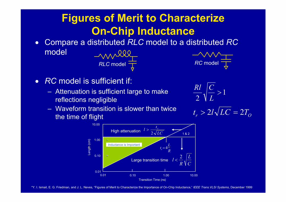
Figures of Merit to Characterize On-Chip Inductance
• Compare a distributed RLC model to a distributed RCmodel
RLC model RC model
• RC model is sufficient if:– Attenuation is sufficient large to make
reflections negligible1
2>
LCRl
– Waveform transition is slower than twice the time of flight Or TLClt 22 =>
Inductance is Important
0.01 0.10 1.00 10.00Transition Time (ns)
1 & 2
0.01
0.10
1.00
10.00
Leng
th (c
m)
tr =4LR
LCtl r
2>High attenuation
CL
Rl 2<Large transition time
*Y. I. Ismail, E. G. Friedman, and J. L. Neves, “Figures of Merit to Characterize the Importance of On-Chip Inductance,” IEEE Trans.VLSI Systems, December 1999

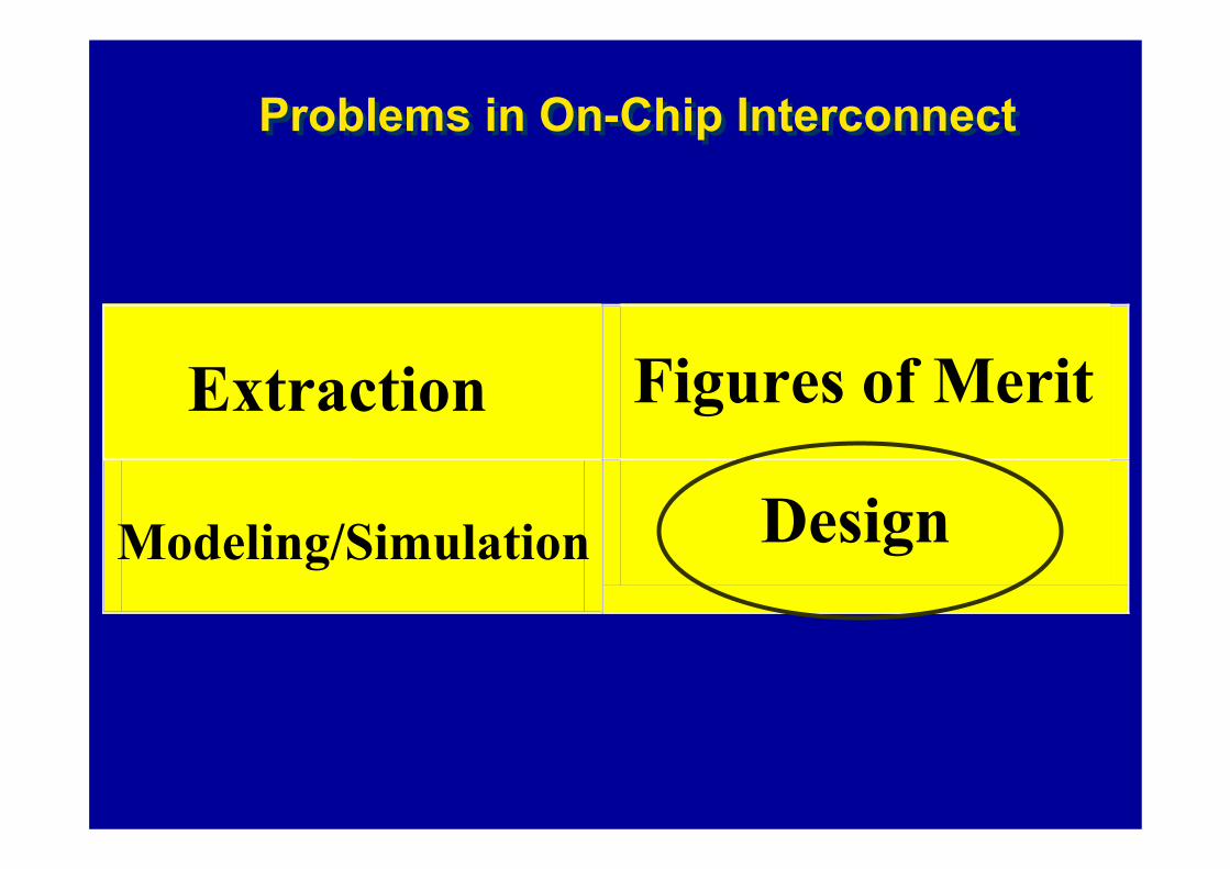
Problems in On-Chip InterconnectProblems in On-Chip Interconnect
Extraction Figures of Merit
Modeling/Simulation Design

• Crosstalk noise (line-to-line coupling)– Voltage variations– Delay uncertainty– Clock jitter– Depends upon wire layout and signal switching pattern
• Capacitive coupling– Short range effects
• Inductive coupling– Long range effects– Depend upon the current return path
• Substrate coupling– Significant issue in mixed-signal circuits– Developing issue in digital circuits
return
curre
nt
Coupled line
aggressor
victim
Interconnect and Substrate Coupling
Problems in On-Chip InterconnectProblems in On-Chip Interconnect
Extraction Figures of Merit
Modeling/Simulation Design
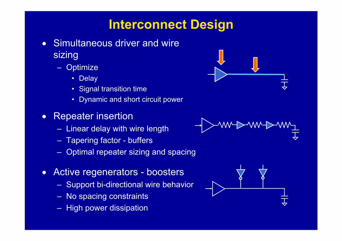
Interconnect Design• Simultaneous driver and wire
sizing– Optimize
• Delay• Signal transition time• Dynamic and short circuit power
• Active regenerators - boosters– Support bi-directional wire behavior– No spacing constraints– High power dissipation
• Repeater insertion– Linear delay with wire length– Tapering factor - buffers – Optimal repeater sizing and spacing

• Shield line insertion can also control inductive crosstalk noise– In addition to reducing capacitive crosstalk noise– Provides a current return path through the shield line for both the aggressor
and victim lines
Shield Line Insertion for Coupled RLC Interconnects

Shielding Efficiency
• Shielding close to the driver may be redundant
– When crosstalk occurs farther from thewire driver
– Peak noise increasesaggressor
Noi
se
driver
Distance
• Achieves a target reduction in noise– Uses minimal metal line resources
• Shielding line density– Tradeoff between
• Noise reduction• Wire routing area
0
10
20
30
40
0 1Cro
ssta
lk N
oise
/ Vd
d (%
)
2 3 4 5 6 7 8 9# of lines between shield
* X. Huang et al. “RLC Signal Integrity Analysis of High-Speed Global Interconnects,” IEEE International Electron Devices Meeting, 2000

Transient Power Tradeoff in Inductive Interconnect
• Dynamic power increases with line width
Dynamic Power
Short-Circuit Power
Total Transient PowerPow
er
Interconnect Width
• Short-circuit power may decrease in underdampedhighly inductive lines
• An optimum interconnect width exists– Minimum transient power
* M. A. El-Moursy and E. G. Friedman, “Power Characteristics of Inductive Interconnect," IEEE Transactions on Very Large Scale Integration (VLSI) Systems, Vol. 12, No. 10, pp. 1295-1306, December 2004

Research Problems
• Develop methodologies to characterize interconnect impedances
• Co-design interconnect drivers with wires– Optimize
• Signal delay• Signal transition time• Reduction in power dissipation
• Unusual physical structures– Next generation packaging – chip interfaces – 3 - D architectures

Agenda
• A historical perspective
• Where are we now ?
⇒Where are we going ?
• Conclusions

Agenda
• A historical perspective
• Where are we now ?
⇒Where are we going ?• One possible solution 3 – D integration
• Conclusions
2L 2
L2
L 2L
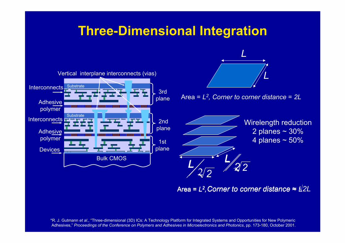
Three-Dimensional Integration
Bulk CMOS
Substrate
Substrate
1st plane
2nd plane
3rd plane
Devices
Adhesive polymer
Adhesive polymer
Interconnects
Interconnects
Vertical interplane interconnects (vias)
*R. J. Gutmann et al., “Three-dimensional (3D) ICs: A Technology Platform for Integrated Systems and Opportunities for New Polymeric Adhesives,” Proceedings of the Conference on Polymers and Adhesives in Microelectronics and Photonics, pp. 173-180, October 2001.
L
L
Area = L2, Corner to corner distance = 2L
Area = L2,Corner to corner distance ≈ √2LArea = L2,Corner to corner distance ≈ L
Wirelength reduction2 planes ~ 30%4 planes ~ 50%
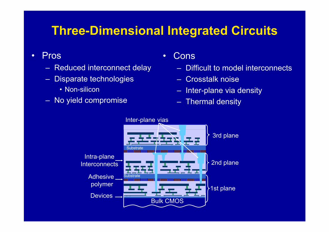
Three-Dimensional Integrated Circuits
• Pros– Reduced interconnect delay– Disparate technologies
• Non-silicon– No yield compromise
• Cons– Difficult to model interconnects – Crosstalk noise– Inter-plane via density– Thermal density
Bulk CMOS
Substrate
Substrate
1st plane
2nd plane
3rd plane
Devices
Adhesive polymer
Intra-planeInterconnects
Inter-plane vias

102
102
Three-dimensional Integration Pros
• Offers greater performance
• Substrate isolation between analog and digital circuits
100 101 102 103 10410-2
100
102
104
106
108
1010
Length in Gate PitchesIn
terc
onne
ct D
ensi
ty F
unct
ion
2-D3-D (2-planes)3-D (4-planes)
*J. Joyner et al., “Impact of Three-Dimensional Architectures on Interconnects in Gigascale Integration,”IEEE Transactions on Very Large Scale Integration (VLSI) Systems, Vol. 9, No. 6, pp. 922-927, December 2001
• Reduction of the length of the longest global interconnects• Decrease in the number of the global interconnects
– The number of local interconnects increases
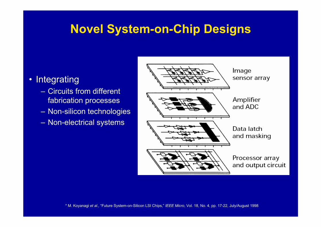
Novel System-on-Chip Designs
• Integrating – Circuits from different
fabrication processes– Non-silicon technologies– Non-electrical systems
* M. Koyanagi et al., “Future System-on-Silicon LSI Chips,” IEEE Micro, Vol. 18, No. 4, pp. 17-22, July/August 1998
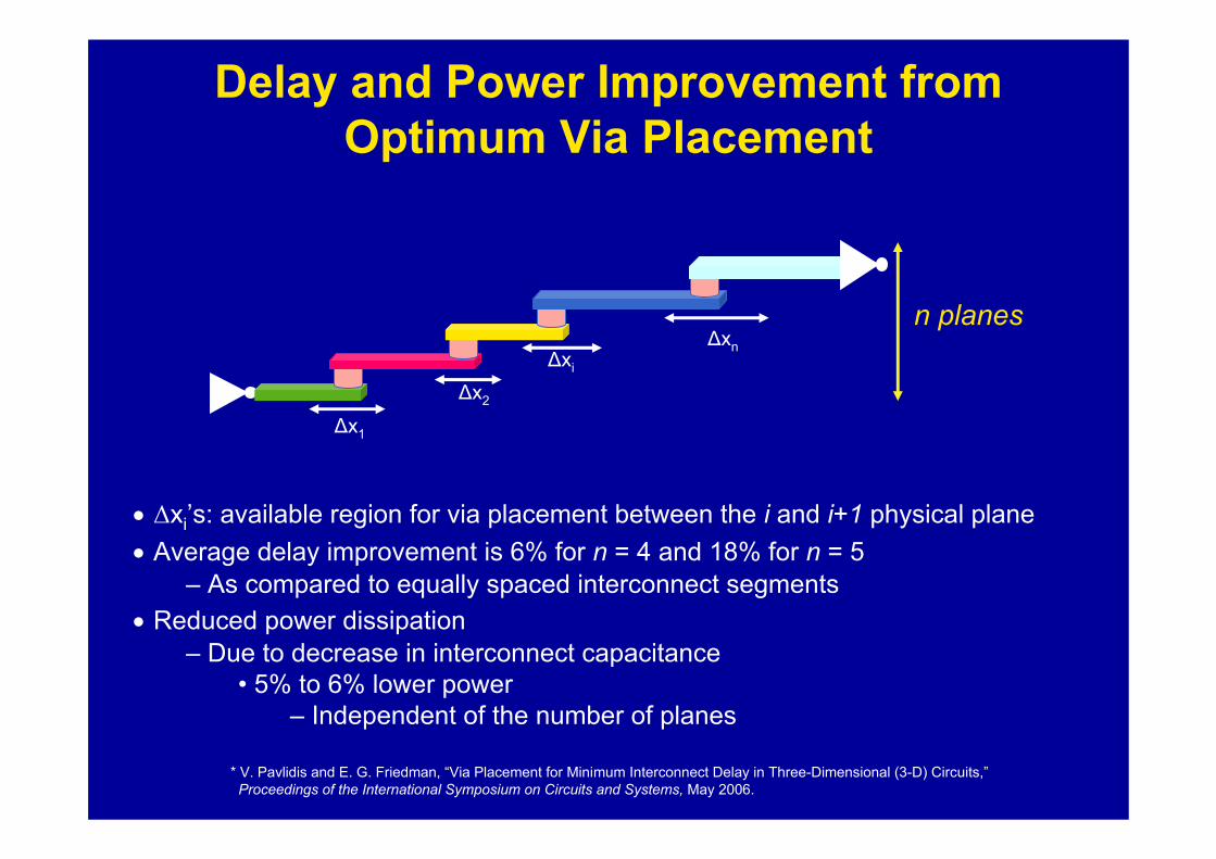
Delay and Power Improvement from Optimum Via Placement
• Δxi’s: available region for via placement between the i and i+1 physical plane• Average delay improvement is 6% for n = 4 and 18% for n = 5
– As compared to equally spaced interconnect segments• Reduced power dissipation
– Due to decrease in interconnect capacitance • 5% to 6% lower power
– Independent of the number of planes
* V. Pavlidis and E. G. Friedman, “Via Placement for Minimum Interconnect Delay in Three-Dimensional (3-D) Circuits,”Proceedings of the International Symposium on Circuits and Systems, May 2006.
Δx1
Δx2
Δxi
Δxn
n planes

Research Problems in 3-D Interconnect Design
• Interplane via placement to efficiently minimize delay
– Interconnect tree structures across multiple planes
• Design expressions which consider inductance
• Optimum via location for lines with repeaters
• Clock distribution networks for 3 – D ICs
• Power distribution structures for 3 – D ICs
• Satisfy heating constraints without compromising performance
• 3 – D NoC
Agenda
• A historical perspective
• Where are we now ?
⇒Where are we going ?• One possible solution 3 – D integration• Another solution Networks on Chip
• Conclusions
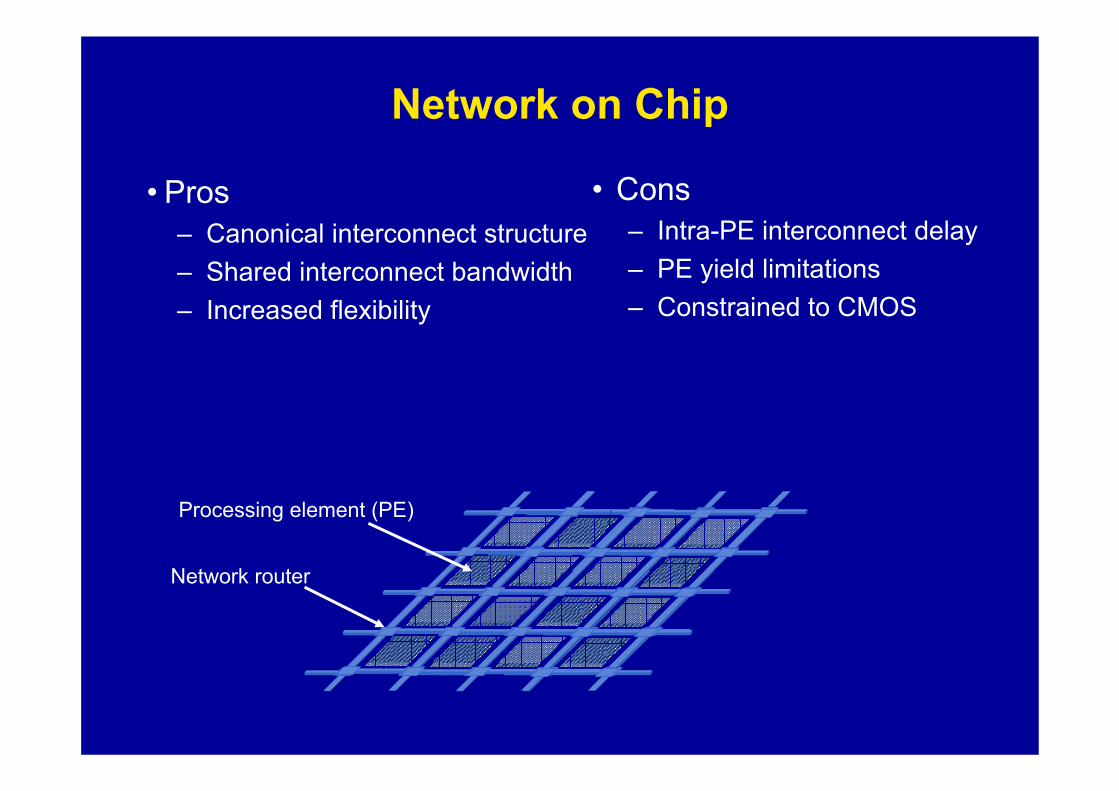
Network on Chip
• Pros– Canonical interconnect structure– Shared interconnect bandwidth– Increased flexibility
• Cons– Intra-PE interconnect delay– PE yield limitations– Constrained to CMOS
Processing element (PE)
Network router
Agenda
• A historical perspective
• Where are we now ?
⇒Where are we going ?• One possible solution 3 – D integration• Another solution Networks on Chip• Why not 3 – D NoC ?
• Conclusions

3-D NoCs
• Pros– Reduced interconnect delay – Canonical interconnect structure– Integration of dissimilar systems
and technologies – No yield limitations– Flexibility
• Design Methodologies
3 – D NoC
?
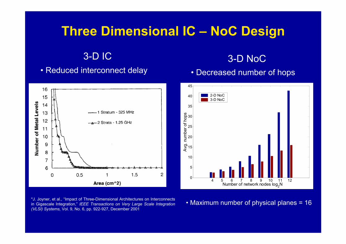
Three Dimensional IC – NoC Design
*J. Joyner, et al., “Impact of Three-Dimensional Architectures on Interconnects in Gigascale Integration,” IEEE Transactions on Very Large Scale Integration (VLSI) Systems, Vol. 9, No. 6, pp. 922-927, December 2001
3-D IC
4 5 6 7 8 9 10 11 120
5
10
15
20
25
30
35
40
45
Avg
. num
ber o
f hop
sNumber of network nodes log2N
2-D NoC3-D NoC
3-D NoC• Reduced interconnect delay • Decreased number of hops
• Maximum number of physical planes = 16

Various Topologies for 3-D Mesh IC - NoC
3-D
2-D
3-D2-DNOC
IC
Reduced number of hops
Best of bothNumber of hops
andChannel length
Shorter channellength
• Smaller number of hops• Asymmetric channel length
– Vertical channel Short interplane vias– Horizontal channel Sidelength of the PE
• 2-D network topology, same number of hops• Additional PE planes lead to reduced channel length
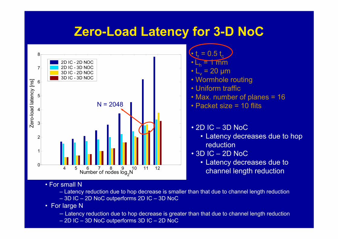
Zero-Load Latency for 3-D NoC• tr = 0.5 tc• Lh = 1 mm• Lv = 20 μm• Wormhole routing• Uniform traffic• Max. number of planes = 16• Packet size = 10 flits
4 5 6 7 8 9 10 11 120
1
2
3
4
5
6
7
8
Zero
-load
late
ncy
[ns]
Number of nodes log2N
2D IC - 2D NOC2D IC - 3D NOC3D IC - 2D NOC3D IC - 3D NOC
N = 2048
• 2D IC – 3D NoC• Latency decreases due to hop
reduction• 3D IC – 2D NoC
• Latency decreases due to channel length reduction
• For small N– Latency reduction due to hop decrease is smaller than that due to channel length reduction– 3D IC – 2D NoC outperforms 2D IC – 3D NoC
• For large N– Latency reduction due to hop decrease is greater than that due to channel length reduction– 2D IC – 3D NoC outperforms 3D IC – 2D NoC

Zero-Load Latency for 3-D NoC• tr = 2 tc• Lh = 1 mm• Lv = 20 μm• Wormhole routing• Uniform traffic• Max. number of planes = 16• Packet size = 10 flits
4 5 6 7 8 9 10 11 120
5
10
15
Zero
-load
late
ncy
[ns]
Number of nodes log2N
2D IC - 2D NOC2D IC - 3D NOC3D IC - 2D NOC3D IC - 3D NOC
N = 512
• tr / tc determines at which N,2D IC – 3D NoC outperforms 3D IC – 2D NoC
– tr = 0.5 tc, N = 2048– tr = 2 tc, N = 512
• Optimum topology 3D IC – 3D NoC– Available physical planes of the stack are optimally distributed to
• Reduce number of hops• Reduce communication channel length
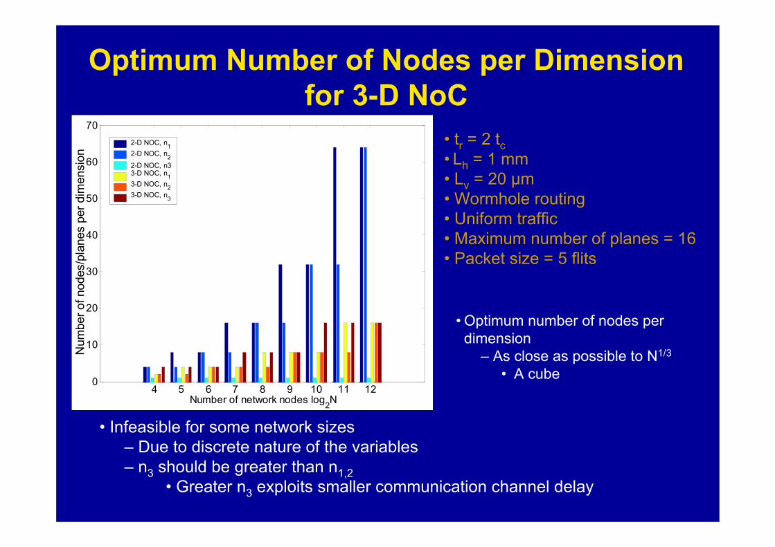
Optimum Number of Nodes per Dimension for 3-D NoC
• tr = 2 tc• Lh = 1 mm• Lv = 20 μm• Wormhole routing• Uniform traffic• Maximum number of planes = 16• Packet size = 5 flits
4 5 6 7 8 9 10 11 120
10
20
30
40
50
60
70
Num
ber o
f nod
es/p
lane
s pe
r dim
ensi
on
Number of network nodes log2N
2-D NOC, n12-D NOC, n22-D NOC, n33-D NOC, n13-D NOC, n23-D NOC, n3
• Optimum number of nodes per dimension
– As close as possible to N1/3
• A cube
• Infeasible for some network sizes– Due to discrete nature of the variables– n3 should be greater than n1,2
• Greater n3 exploits smaller communication channel delay

Agenda
• A historical perspective
• Where are we now ?
• Where are we going ?
⇒Conclusions

Conclusions
• The trends are clear– Interconnect now dominates the design process
• Different aspects of the interconnect design process– Figures of merit– Extraction– Modeling and simulation – Interconnect-aware design methodologies
• 3 – D integration is coming– NoC is here and important for on-chip global data transfer
• 3 – D NoC– A natural evolution

Any Questions
?

Back-Up Viewgraphs

Aluminum vs Copper Characteristics
• Aluminum lines – Larger coupling capacitance– Larger coupling noise
• Copper lines– Lower resistance– Inductance effects are more significant in wider lines
* X. Huang et al., “RLC Signal Integrity Analysis of High-Speed Global Interconnects,” IEEE International Electron Devices Meeting, 2000
25
30
35
40
0.8/0.6 1.2/0.8 2.5/1.25 5/2.5
Al Cu
Cro
ssta
lk N
oise
/ V
dd (%
)
Line Size (um)
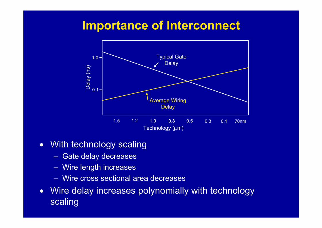
Importance of Interconnect
• With technology scaling– Gate delay decreases– Wire length increases– Wire cross sectional area decreases
• Wire delay increases polynomially with technology scaling
Typical GateDelay
Average WiringDelay
0.1
1.0
Del
ay (n
s)
1.5 1.01.2 0.8 0.30.5Technology (μm)
0.1 70nm
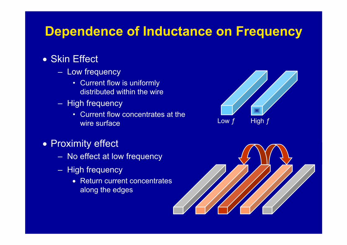
Dependence of Inductance on Frequency
• Skin Effect– Low frequency
• Current flow is uniformly distributed within the wire
– High frequency• Current flow concentrates at the
wire surface
• Proximity effect– No effect at low frequency– High frequency
• Return current concentrates along the edges
Low ƒ High ƒ
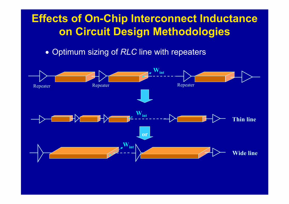
Effects of On-Chip Interconnect Inductance on Circuit Design Methodologies
• Optimum sizing of RLC line with repeaters
RepeaterRepeater Repeater
Wint
Thin lineWint
Wide lineWint
or
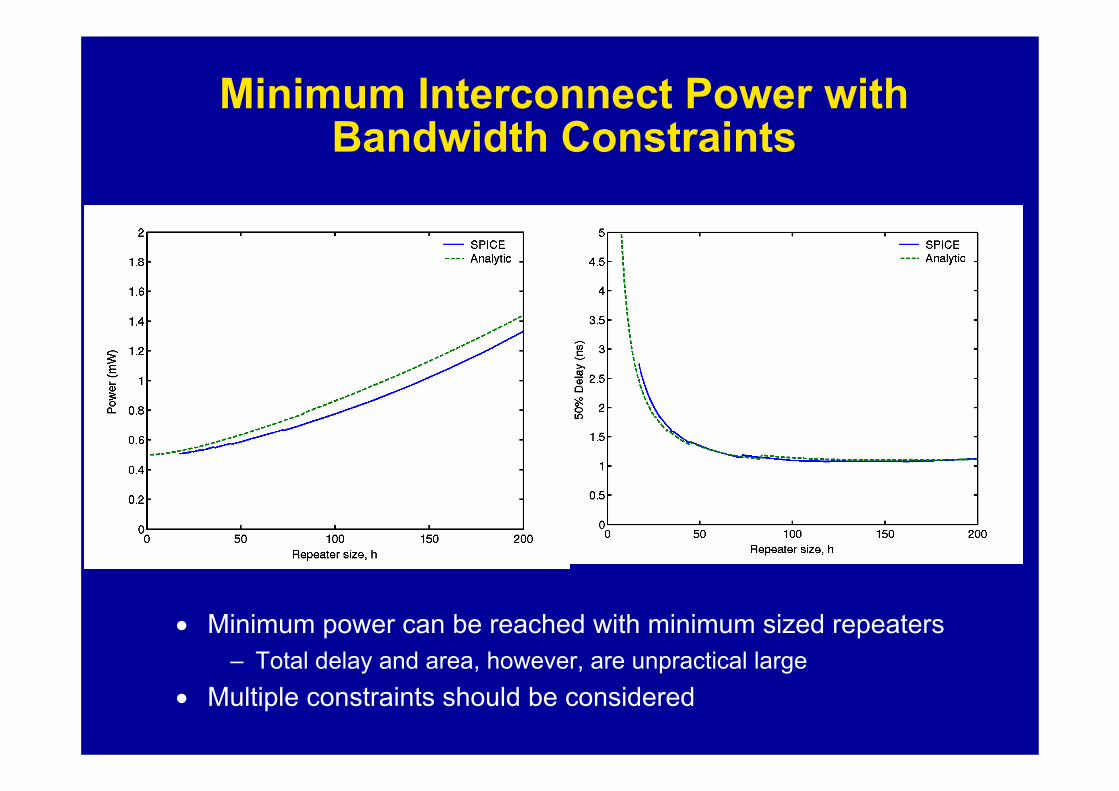
Minimum Interconnect Power with Bandwidth Constraints
• Minimum power can be reached with minimum sized repeaters– Total delay and area, however, are unpractical large
• Multiple constraints should be considered

• Shielding for high speed interconnect– Develop crosstalk noise model and shielding techniques for
coupled RLC interconnects– Develop shielding techniques to minimize power and delay under
crosstalk noise constraints– Develop a shielding methodology to minimize delay and crosstalk
noise
Current Research Plans
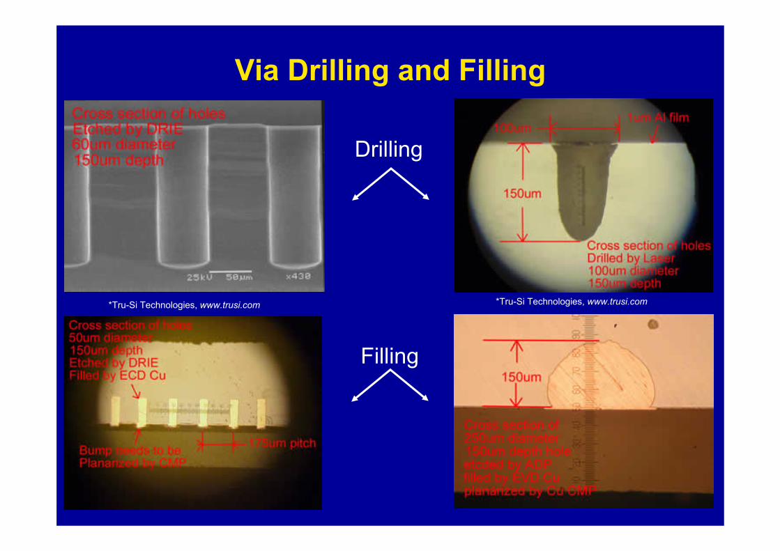
Via Drilling and Filling
*Tru-Si Technologies, www.trusi.com
Drilling
Filling
*Tru-Si Technologies, www.trusi.com
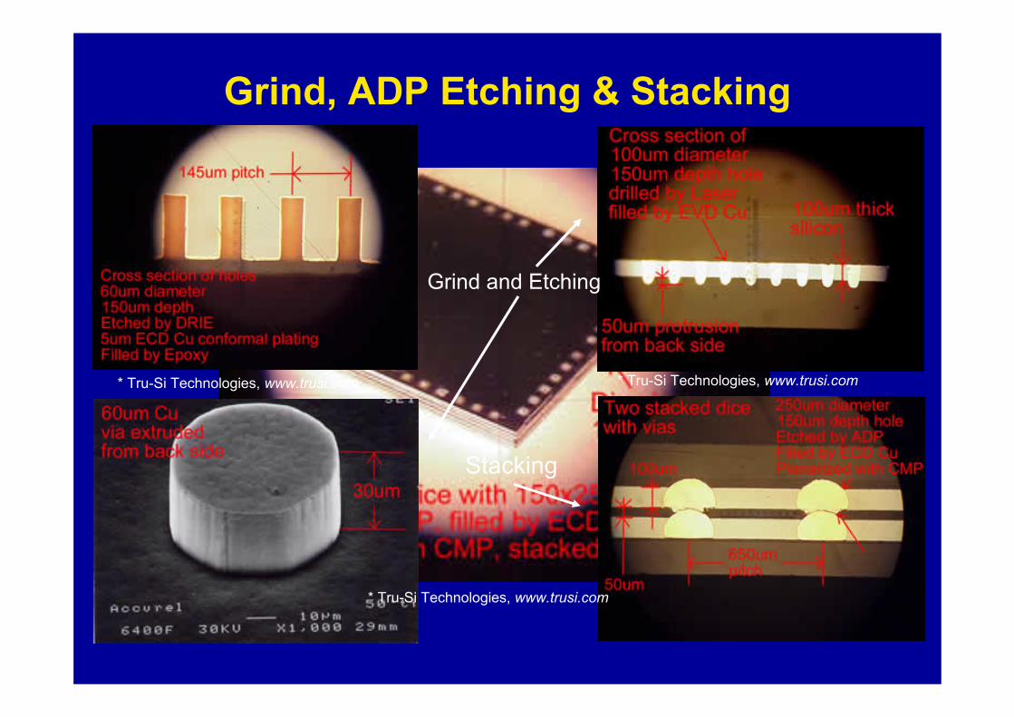
Grind, ADP Etching & Stacking
* Tru-Si Technologies, www.trusi.com
Grind and Etching
Stacking
* Tru-Si Technologies, www.trusi.com * Tru-Si Technologies, www.trusi.com

Existing Work in 3-D Integration
• Fabrication techniques – Copper wafer bonding – Adhesion with polymers
• Heating Effects and Constraints
* S. Tiwari et al., “Three-dimensional Integration in Silicon Electronics,” Proceedings of Lester Eastman Conference, pp. 24-33, 2002
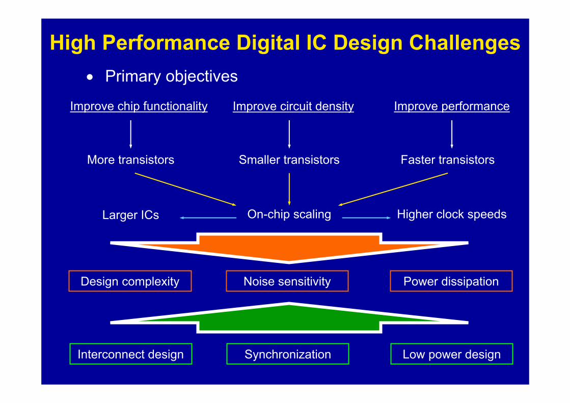
High Performance Digital IC Design Challenges• Primary objectives
Improve chip functionality Improve circuit density Improve performance
On-chip scaling Higher clock speedsLarger ICs
More transistors Smaller transistors Faster transistors
Design complexity Noise sensitivity Power dissipation
Interconnect design Synchronization Low power design
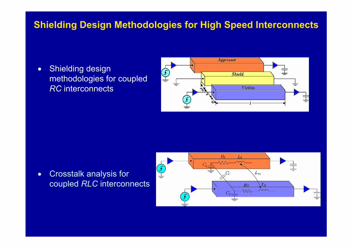
• Shielding design methodologies for coupled RC interconnects
• Crosstalk analysis for coupled RLC interconnects
Shielding Design Methodologies for High Speed Interconnects
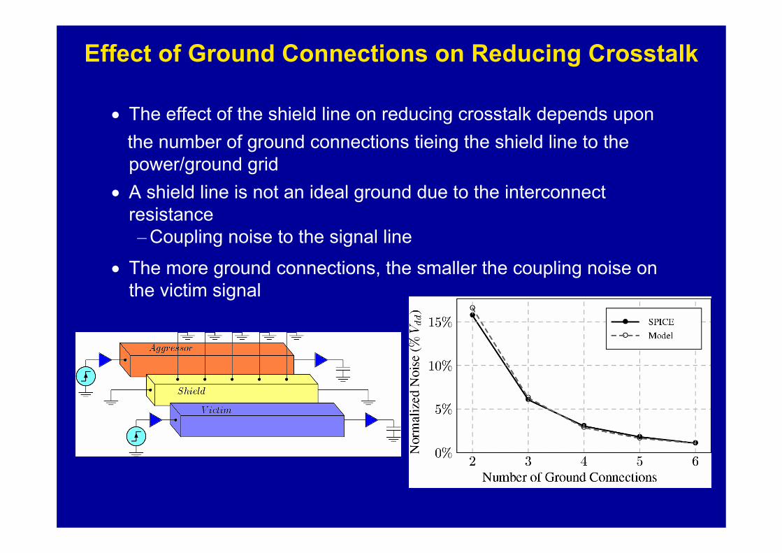
• The effect of the shield line on reducing crosstalk depends uponthe number of ground connections tieing the shield line to the power/ground grid
• A shield line is not an ideal ground due to the interconnect resistance– Coupling noise to the signal line
• The more ground connections, the smaller the coupling noise on the victim signal
Effect of Ground Connections on Reducing Crosstalk

Repeater Insertion with Delay Constraints
• A design space of repeaters is determined by delay constraint
• With TreqTmin, design space converges to the delay optimum repeater system (hopt,kopt)
* G. Chen and E. G. Friedman, “Low Power Repeaters Driving RC Interconnects with Delay and Bandwidth Constraints,”Proceedings of the SOC Conference, pp. 335-339, September 2004

Minimum Power with Both Delay and Bandwidth Constraints
• Satisfactory design occurs at the intersection of the two designspaces with delay and bandwidth constraints
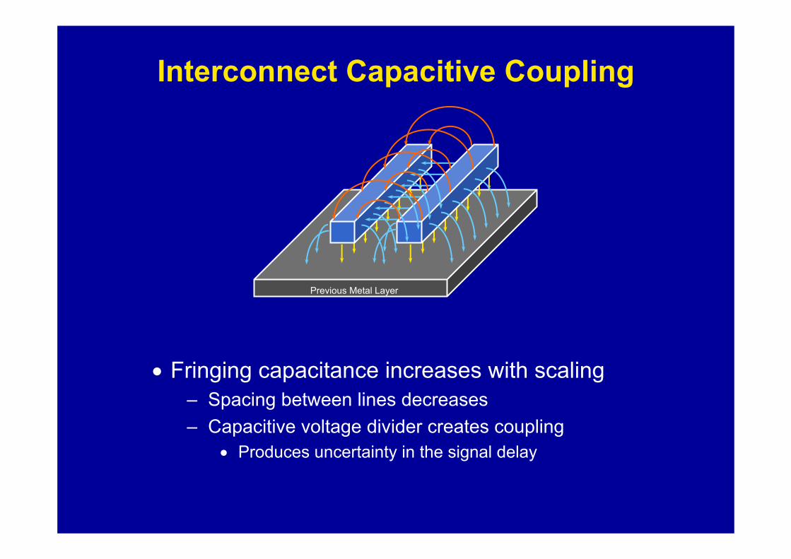
Interconnect Capacitive Coupling
• Fringing capacitance increases with scaling – Spacing between lines decreases– Capacitive voltage divider creates coupling
• Produces uncertainty in the signal delay
Previous Metal Layer

Capacitive Coupling Noise
• Signal coupling– Crosstalk– Aggressor – victim model
• Aggressor: line generating noise• Victim: noise sensitive line
• Variations in signal delay– Simultaneous switching noise– Variations in effective coupling
capacitance
C1C2
aggressor
victim
*K. T. Tang and E. G. Friedman.,” Delay and Noise Estimation of CMOS Logic Gates Driving Coupled Resistive-Capacitive Interconnections,” Integration, September 2000
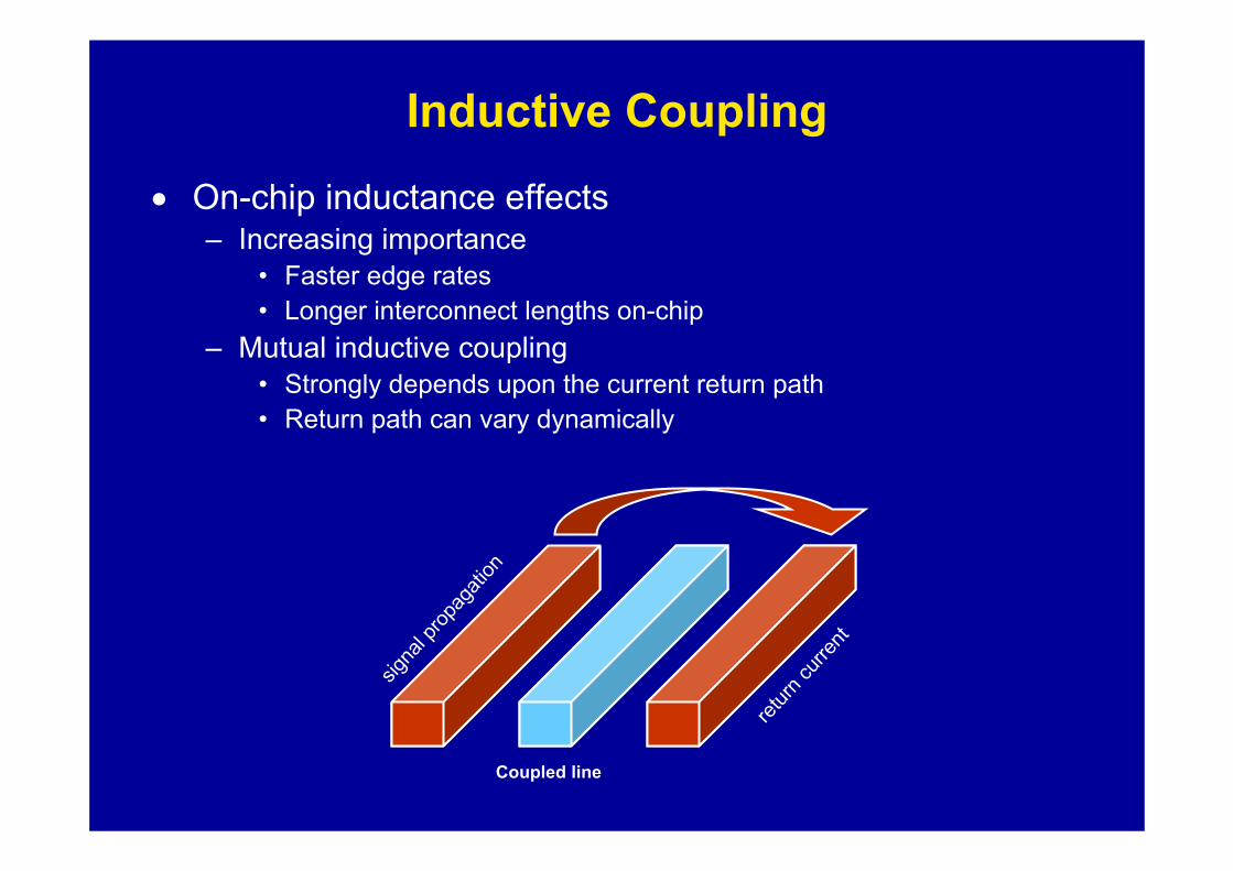
Inductive Coupling
• On-chip inductance effects– Increasing importance
• Faster edge rates• Longer interconnect lengths on-chip
– Mutual inductive coupling• Strongly depends upon the current return path• Return path can vary dynamically
signa
l prop
agati
on
return
curre
nt
Coupled line

Interconnect Shielding
• Insert power lines among signal lines– Isolates an aggressor (noisy) line from
sensitive neighboring lines– Increases the noise tolerance of a
sensitive line
• Reduces capacitive coupling– The voltage of the shield lines typically does not switch– Reduces variations of the effective line capacitance
• Reduced delay uncertainty
• Controls mutual inductance effects– The current return path is clearly determined
Signalline
Signalline
Signalline
VDDline
GNDline

Geometric Wire Characteristics• Narrow lines
– RC dominant – Quadratic delay with
line length
2025
30
35
40
45
50
1 2 3 4 5 6 7 8 9
W0.8 S0.6
Line Length (mm)
Cro
ssta
lk N
oise
/ Vd
d (%
)
W1.2 S0.8W2.5 S1.25
1 2 3 4 5 6 7 8 9 1050
100
150
200250
300
350
Del
ay (p
s)
Line Length (mm)
W0.8 S0.6W1.2 S0.8W2.5 S1.25
• Wide lines– Less noise at the far end– Delay is linearly dependent on
line length– Inductive behavior
* X. Huang et.al. “RLC Signal Integrity Analysis of High-Speed Global Interconnects,” IEEE International Electron Devices Meeting, 2000

• Techniques to reduce crosstalk between coupled interconnects– Increase separation– Insert a shield line
• Inserting a shield line is more effective in reducing crosstalk than increasing the separation
Standard Techniques for Reducing Line-to-Line Crosstalk
* J. Zhang and E. G. Friedman, “Crosstalk Noise Model for Shielded Interconnects in VLSI-Based Circuits," Proceedings of the IEEE International SOC Conference, pp. 243-244, September 2003

Effect of Shield Insertion on Reducing Crosstalk Noise
• Three interconnect structures of one/two/three shield lines – Three shield structure has the least
crosstalk noise– Two shield structure reduces the
crosstalk noise to a level comparable to three shield structure
– One shield structure has lower noise than two shield structure• Without considering other neighboring
lines
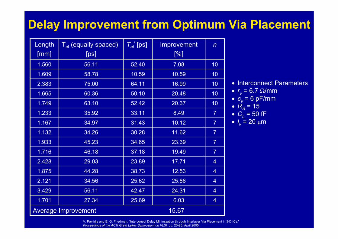
Delay Improvement from Optimum Via Placement
• Interconnect Parameters• rv = 6.7 Ω/mm• cv = 6 pF/mm • RS = 15• CL = 50 fF• lv = 20 μm
Average Improvement 15.6746.0325.6927.341.701
424.3142.4756.113.429
425.8625.6234.562.121
412.5338.7344.281.875
417.7123.8929.032.428
719.4937.1846.181.716
723.3934.6545.231.933
711.6230.2834.261.132
710.1231.4334.971.167
78.4933.1135.921.233
1020.3752.4263.101.749
1020.4850.1060.361.665
1016.9964.1175.002.383
1010.5910.5958.781.609
107.0852.4056.111.560
nImprovement[%]
Tel* [ps]Tel (equally spaced)
[ps]Length [mm]
V. Pavlidis and E. G. Friedman, “Interconect Delay Minimization through Interlayer Via Placement in 3-D ICs," Proceedings of the ACM Great Lakes Symposium on VLSI, pp. 20-25, April 2005.