optical and electrical properties of conducting polymer-functionalized carbon nanotubes...
TRANSCRIPT

Contents lists available at ScienceDirect
Materials Science in Semiconductor Processing
Materials Science in Semiconductor Processing 22 (2014) 7–15
http://d1369-80
n CorrE-m
chehata
journal homepage: www.elsevier.com/locate/mssp
Optical and electrical properties of conductingpolymer-functionalized carbon nanotubes nanocomposites
Nadia Chehata n, Adnen Ltaief, Rabeb Bkakri, Abdelaziz BouaziziEquipe Dispositifs Electroniques Organiques et Photovoltaïques Moléculaires, Laboratoire de la Matière Condensée et des Nanosciences,Faculté des Sciences de Monastir, Avenue de L'Environnement, 5019 Monastir, Tunisia
a r t i c l e i n f o
Available online 19 February 2014
Keywords:Conjugated polymerFunctionalized carbon nanotubesCharge transferPhotovoltaic effectConductivity
x.doi.org/10.1016/j.mssp.2014.02.01001 & 2014 Elsevier Ltd. All rights reserved.
esponding author. Tel.: þ216 73 50 02 76; faail addresses: [email protected],[email protected] (N. Chehata).
a b s t r a c t
The effects of incorporating functionalized multiwall carbon nanotubes with polystyrene(PSMWCNTs) in organic polymer solar cells were studied. Different concentrations ofcarbon nanotubes in poly(2-methoxy-5-(2-ethyhexyl-oxy)-p-phenylenevinylene) [MEH-PPV] were investigated via absorption spectroscopy, photoluminescence (PL) and current–voltage measurements under illumination, in order to determine the photovoltaic effect ofthe elaborated organic solar cells. The decrease in PL intensity with the progressiveaddition of PSMWCNTs is a signature of an effective charge transfer at MEH-PPV/PSMWCNTs heterojunction. Moreover, the addition of carbon nanotubes (CNTs) to thepolymer increases the power conversion efficiency compared with the device withpristine polymer. A critical concentration value of 0.15 wt% of PSMWCNTs is found toachieve the best performance of devices. Direct current conductivity of the composite filmwas found to increase rapidly with the increase in PSMWCNTs concentration. Theenhancement in conductivity is explained in terms of percolation theory with anestimated percolation threshold of 0.092 wt%.
& 2014 Elsevier Ltd. All rights reserved.
1. Introduction
To decrease the cost of conventional solar electricity and toensure environment-friendly manufacturing technologies, agreat deal of efforts have driven studies on unconventionalphotovoltaic (PV) device fabrication methodologies usingearth renewable and abundant materials. One of the technol-ogies that has emerged from these efforts is organic photo-voltaics (OPVs) [1–4]. The photovoltaic devices based onorganic materials, including materials [5], production pro-cesses [6] and device architectures have attracted muchinterest of researchers[7]. Particularly, the organic photovol-taics based on conjugated polymers have an attractive feature,as they can be fabricated by a solution coating process (spin
x: þ216 73 50 02 78.
coating or inkjet printing) to cover large areas, and may beformed on flexible plastic substrates [8]. The photoexcitationof a conjugated polymer, a typical light absorber material, willgenerate an electron–hole pair quasi-particle bounded byelectrostatic force and called an exciton [9]. Cells based on asingle polymer layer sandwiched between two electrodestend to be inefficient because the dissociation of photogener-ated excitons is not usually ensured at polymer/metaljunction. The defining feature of OPVs needs the use of two-component donor–acceptor photoactive materials, whichperform the function of light absorption, charge transfer andgeneration of photocurrent. If the photogenerated excitonreaches the interface, between the polymer donor and thehigher electron affinity acceptor, charge transfer process willoccur with electron transfer to the acceptor. So far, theresearch efforts of OPV materials has been concentrated onpoly(3-hexylthiophene) (P3HT) as donor and [6,6]-phenyl-C61- butyric acid methyl ester (PCBM) as acceptor. However,

Fig. 1. (a) Chemical structure of poly(2-methoxy, 5-(2-ethyl-hexyloxy)-p-phenyl vinylene) [MEH-PPV], (b) TEM image of investigated MWCNTs [37], and(c) chemical structure of poly(ethylenedioxy-thiophene): poly(styrene sulfonate) [PEDOT:PSS].
N. Chehata et al. / Materials Science in Semiconductor Processing 22 (2014) 7–158
the power conversion efficiency of these OPV devices is stilllow compared to conventional inorganic devices [10]. This hasled to study of other allotropic forms of carbon nanomaterialsas acceptors, including carbon nanotubes (CNTs) [11,12].Carbon nanotubes have intrigued researchers due to theirexcellent physical and chemical properties, such as highcarrier mobility, high aspect ratio, huge current carryingcapability, and large specific surface [13]. With advantagesfrom these exceptional properties, the use of CNTs as anacceptor material within bulk heterojunction structureenables to the amelioration of polymer OPVs efficiency[14–17]. It is proposed that the enhancement in the photo-voltaic properties of the blend device is due to the introduc-tion of internal polymer/nanotube junctions within thepolymer matrix [17]. These junctions act as sites for excitondissociation and also create a continuous pathway for theelectrons to be efficiently transported to the negative elec-trode. Hence, effective volume of exciton dissociation centerswas much higher in CNTs based devices. This results in anincrease in the electron mobility, and hence balances thecharge carrier transport to the electrodes. In addition theconductivity of the nanocomposite is increased, indicatingpercolation paths within the material [18]. However, a majorchallenge for their use in polymer matrix is to achievehomogeneous dispersion, as CNTs exist in the form ofaggregates due to strong van der Waals forces originatingfrom their small size and large surface area [19]. Differenttechniques are often used to prepare polymer/CNTs nano-composites, such as: (i) in situ polymerization of the mono-mers in the presence of CNTs [20], (ii) solution casting whereboth thematrix polymer and CNTs are dispersed in a commonsolvent followed by evaporation [21], and (iii) melt processingwhich involves mechanical mixing of the molten polymersand CNTs [22]. Besides, for better dispersion and interfacialadhesion of CNTs in host polymers, chemical modificationor functionalization of CNTs is needed in order to increasetheir compatibility with polymers [23–25]. Mostly, the
functionalization of CNTs with a polymer will ensure chemicalcompatibility between donor polymer and CNTs acceptor [26].Due to these several features of conducting polymer/CNTsnanocomposites, it is very interesting to investigate the effectof CNTs functionalization on optical and electrical propertiesof polymer/CNTs nanocomposites.
In the present work, we have investigated the optical andelectrical properties of MEH-PPV:PSMWCNTs nanocompositein solutions and thin films. MEH-PPV is among the moststudied conjugated polymers for its luminescence propertiesand has been considered as hole transporting semiconductorfor making organic [27] and hybrid solar cells [28]. Theinvestigated MWCNTs were functionalized with polystyrene(PS) to form PSMWCNTs fillers. Both in solution and thin film,it is observed that the photoluminescence (PL) of the nano-composites decrease progressively with the increase ofMWCNTs concentration, indicating a fast transfer of photo-induced electrons from donor polymer to acceptor nanotubes.Further, the device based on ITO/PEDOT:PSS/MEH-PPV:PSMWCNTs/Al shows a photovoltaic effect with ameliorationof device performance until 0.15 wt% of PSMWCNTs. Theelectrical conductivity study reveals a percolation thresholdconcentration of 0.092 wt% of PSMWCNTs in polymer matrix.
2. Experimental details
2.1. Materials
MEH-PPV was purchased from Sigma-Aldrich and themolecular weight of the MEH-PPV was 86.000 g/mol. Themolecular structure of MEH-PPV is presented in Fig. 1a.MWCNTs (Graphistrength™ C100) were supplied by ARKEMA(Fig. 1b) [29] and used without further purification. MEH-PPVis a straight-chain conjugated polymer. One might expectMEH-PPV to bind to MWCNTs, based on the chemicalsimilarity of the conjugated backbones of both conjugatedmaterials, and given the right solvent environment [30].
MWCNTs PS-MWCNTs
Fig. 3. Solubility behavior of (a) pristine carbon nanotubes and(b) functionalized carbon nanotubes.
2.9 eV
5.3 eV5.1 eV5 eV
Al
4.3 eV
ITO
4.8 eV
MEH-PPV PSMWCNTsPEDOT-PSS
Fig. 4. Energy band diagram of investigated solar devices. Al and ITO areused as cathode and anode, respectively.
N. Chehata et al. / Materials Science in Semiconductor Processing 22 (2014) 7–15 9
Functionalization process of MWCNTs by polystyrene (PS) wasdescribed elsewhere [31]. Poly(ethylenedioxy-thiophene):poly(styrene sulfonate) [PEDOT:PSS] (Fig. 1c), commonlyinvestigated as the hole-injection layer in organic solar cellsdevices for its simplicity and high efficiency, was used as hole-injection layer. The common solvent to disperse MEH-PPV andPSMWCNTs is chloroform.
2.2. Substrate preparation
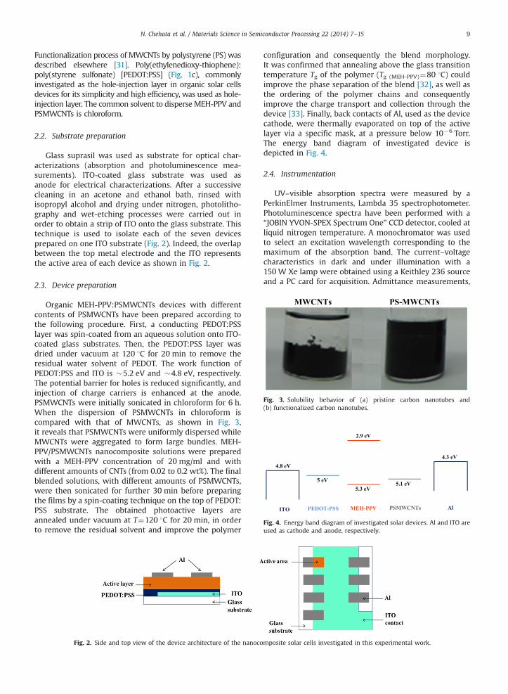
Glass suprasil was used as substrate for optical char-acterizations (absorption and photoluminescence mea-surements). ITO-coated glass substrate was used asanode for electrical characterizations. After a successivecleaning in an acetone and ethanol bath, rinsed withisopropyl alcohol and drying under nitrogen, photolitho-graphy and wet-etching processes were carried out inorder to obtain a strip of ITO onto the glass substrate. Thistechnique is used to isolate each of the seven devicesprepared on one ITO substrate (Fig. 2). Indeed, the overlapbetween the top metal electrode and the ITO representsthe active area of each device as shown in Fig. 2.
2.3. Device preparation
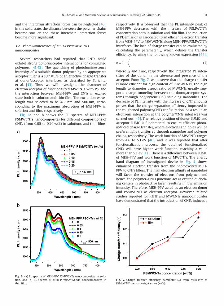
Organic MEH-PPV:PSMWCNTs devices with differentcontents of PSMWCNTs have been prepared according tothe following procedure. First, a conducting PEDOT:PSSlayer was spin-coated from an aqueous solution onto ITO-coated glass substrates. Then, the PEDOT:PSS layer wasdried under vacuum at 120 1C for 20 min to remove theresidual water solvent of PEDOT. The work function ofPEDOT:PSS and ITO is �5.2 eV and �4.8 eV, respectively.The potential barrier for holes is reduced significantly, andinjection of charge carriers is enhanced at the anode.PSMWCNTs were initially sonicated in chloroform for 6 h.When the dispersion of PSMWCNTs in chloroform iscompared with that of MWCNTs, as shown in Fig. 3,it reveals that PSMWCNTs were uniformly dispersed whileMWCNTs were aggregated to form large bundles. MEH-PPV/PSMWCNTs nanocomposite solutions were preparedwith a MEH-PPV concentration of 20 mg/ml and withdifferent amounts of CNTs (from 0.02 to 0.2 wt%). The finalblended solutions, with different amounts of PSMWCNTs,were then sonicated for further 30 min before preparingthe films by a spin-coating technique on the top of PEDOT:PSS substrate. The obtained photoactive layers areannealed under vacuum at T¼120 1C for 20 min, in orderto remove the residual solvent and improve the polymer
Fig. 2. Side and top view of the device architecture of the nanoco
configuration and consequently the blend morphology.It was confirmed that annealing above the glass transitiontemperature Tg of the polymer (Tg (MEH-PPV)¼80 1C) couldimprove the phase separation of the blend [32], as well asthe ordering of the polymer chains and consequentlyimprove the charge transport and collection through thedevice [33]. Finally, back contacts of Al, used as the devicecathode, were thermally evaporated on top of the activelayer via a specific mask, at a pressure below 10�6 Torr.The energy band diagram of investigated device isdepicted in Fig. 4.
2.4. Instrumentation
UV–visible absorption spectra were measured by aPerkinElmer Instruments, Lambda 35 spectrophotometer.Photoluminescence spectra have been performed with a“JOBIN YVON-SPEX Spectrum One” CCD detector, cooled atliquid nitrogen temperature. A monochromator was usedto select an excitation wavelength corresponding to themaximum of the absorption band. The current–voltagecharacteristics in dark and under illumination with a150 W Xe lamp were obtained using a Keithley 236 sourceand a PC card for acquisition. Admittance measurements,
mposite solar cells investigated in this experimental work.

N. Chehata et al. / Materials Science in Semiconductor Processing 22 (2014) 7–1510
carried out in dark, have been performed with a Solartronimpedance/gain-phase analyzer SI 1260. All these mea-surements have been performed under room conditions.
3. Results and discussion
3.1. Absorption of MEH-PPV:PSMWCNTs nanocomposites
Fig. 5a shows the absorption spectra of MEH-PPV andMEH-PPV:PSMWCNTs nanocomposites in solution and withdifferent CNT concentrations (0.05, 0.10, 0.15 and 0.20 wt%).The strongest absorption peak of pure MEH-PPV in solutionis located at λ¼487 nm. By the addition of PSMWCNTs, theabsorption spectrum of MEH-PPV is broadened in UV and IRregions. This feature might be related to some interactionbetween polymer and CNTs and/or to the modification ofpolymer conformation chain when CNTs are introduced.From this point of view, one would expect that theseinteractions are maximized in the solid state. Thus, a setof thin films of MEH-PPV and nanocomposites with thesame range of concentrations was prepared by the spincoating technique. From Fig. 5b, we can note that MEH-PPVmain peak (centered at 500 nm) is redshifted with the
200 300 400 500 600 700 800 900
0.0
0.2
0.4
0.6
0.8
Abs
orpt
ion
Inte
nsity
(a. u
. )
Wavelength λ (nm)
MEH-PPV:PSCNTs (wt %) 0 0.05 0.10 0.15 0.20
0.00 0.05 0.10 0.15 0.20
0.88
0.92
0.96
PSCNTs Concentration (wt %)
Maximum absorption intensity
λmax (nm)
500
502
504
506
Fig. 5. (a) Absorption spectra of MEH-PPV:PSMWCNTs nanocomposites in solutiofilm, (c) variation of absorption maximum intensity and λmax versus PSMWCNTssolution and thin film.
increase of CNT concentrations. However, a redshift in theπ–πn absorption peak of MEH-PPV is not necessarily asignature of a ground state interaction, but is often relatedto an increase in π-electron delocalization along the poly-mer chain in the presence of CNTs [12]. This behavior hasbeen found previously, where an increase of polymerconjugation length is observed in poly(p-phenylene viny-lene) (PPV) derivatives:MWCNTs nanocomposites whenMWCNTs content is increased [34,35]. Musumeci et al.[36] have shown the tendency for polymer chain alignmentwith the CNT main axis in the case of P3HT/MWCNTsnanocomposites. Thus the incorporation of CNTs modifiesthe MEH-PPV polymer structure, promoting polymer order-ing and higher crystallinity [37,38]. Besides, the absorptionintensity of MEH-PPV filmwas decreased by the progressiveaddition of CNTs. This behavior is probably related to thereduction in the optical volume of MEH-PPV when CNTswere progressively added [39]. Variation in position andintensity of main peak for the MEH-PPV/PSMWCNTs nano-composites in thin film is illustrated in Fig. 5c. The absorp-tion spectra of MEH-PPV in solution and thin film depictedthe main absorption peak at 485 and 500 nm, respectively(Fig. 5d). In the dilute solution, polymer chains are isolated
300 400 500 600 700
0.0
0.2
0.4
0.6
0.8
1.0
Abs
orpt
ion
Inte
nsity
(a. u
. )
Wavelength λ (nm)
MEH-PPV:PSCNTs (wt %) 0 0.05 0.10 0.15 0.20
300 350 400 450 500 550 600 650
0.0
0.2
0.4
0.6
0.8
1.0
λmax= 485 nm
λmax= 500 nm
Abs
orpt
ion
Inte
nsity
(a. u
. )
Wavelength λλ (nm)
Film Solution
n, (b) absorption spectra of MEH-PPV:PSMWCNTs nanocomposites in thincontent, and (d) comparison of absorption spectra of pristine MEH-PPV in
N. Chehata et al. / Materials Science in Semiconductor Processing 22 (2014) 7–15 11
and the interchain attraction forces can be neglected [40].In the solid state, the distance between the polymer chainsbecome smaller and these interchain interaction forcesbecome more significant.
3.2. Photoluminescence of MEH-PPV:PSMWCNTsnanocomposites
Several researchers had reported that CNTs couldexhibit strong donor/acceptor interactions for conjugatedpolymers [41,42]. The quenching of photoluminescenceintensity of a suitable donor polymer by an appropriateacceptor filler is a signature of an effective charge transferat donor/acceptor interfaces, as described by Sariciftciet al. [43]. Thus, we will investigate the character ofelectron acceptor of functionalized MWCNTs with PS, andthe interaction between MEH-PPV and CNTs in excitedstate both in solution and thin film. The excitation wave-length was selected to be 485 nm and 500 nm, corre-sponding to the maximum absorption of MEH-PPV insolution and film, respectively.
Fig. 6a and b shows the PL spectra of MEH-PPV:PSMWCNTs nanocomposites for different compositions ofCNTs (from 0.05 to 0.20 wt%) in solutions and thin films,
550 600 650 700 750 800
1500
1750
2000
2250
2500
2750
λ = 500 nm
PL In
tens
ity (a
. u.)
Wavelength λ (nm)
MEH-PPV:PSCNTs ( wt %) 0 0.05 0.1 0.15 0.2
550 600 650 700 750 800
1500
1750
2000
2250
2500
PL In
tens
ity (a
. u. )
Wavelength λ (nm)
MEH-PPV: PSMWCNTs (wt %)00.05 0.10 0.15 0.20
λ = 487 nm
Fig. 6. (a) PL spectra of MEH-PPV:PSMWCNTs nanocomposites in solu-tion, and (b) PL spectra of MEH-PPV:PSMWCNTs nanocomposites inthin film.
respectively. It is observed that the PL intensity peak ofMEH-PPV decreases with the increase of PSMWCNTsconcentration both in solution and thin film. The reductionof PL emission is associated to an efficient electron transferfrom MEH-PPV to PSMWCNTs along MEH-PPV:PSMWCNTsinterfaces. The load of charge transfer can be evaluated bycalculating the parameter η, which defines the transferefficiency, by using the following known expression [44]:
η¼ 1� II0
ð1Þ
where I0 and I are, respectively, the integrated PL inten-sities of the donor in the absence and presence of theacceptor. From Fig. 7, we observe that the charge transferis more efficient for high content of PSMWCNTs. The highlength to diameter aspect ratio of MWCNTs greatly sup-ports charge tunneling between the donor/acceptor sys-tems through polystyrene (PS) shielding nanotubes. Thedecrease of PL intensity with the increase of CNT amountsproves that the charge separation efficiency improved inthe roughened polymer/CNTs configuration. As a result, anelectronic interaction at the polymer/CNTs interfaces wascarried out [45]. The relative position of donor LUMO andacceptor LUMO is fundamental to ensure efficient photo-induced charge transfer, where electrons and holes will bepreferentially transferred through nanotubes and polymerchains, respectively. The work function of MWCNTs rangesfrom 4.6 to 5.1 eV [46], and it was reported that afterfunctionalization process, the obtained functionalizedCNTs will have higher work function, reaching a valuemore than 5.1 eV [11]. There is a difference between LUMOof MEH-PPV and work function of MWCNTs. The energyband diagram of investigated device in Fig. 4 showsenhanced electron transfer from the photoexcited MEH-PPV to CNTs fillers. The high electron affinity of nanotubeswill favor the transfer of electrons from polymer, andhence, the polymer–CNTs junctions act as exciton quench-ing centers in photoactive layer, resulting in low emissionintensity. Therefore, MEH-PPV acted as an electron donorand PSMWCNTs as electron acceptor. However, relatedstudies reported for P3HT and MWCNTs nanocompositeshave demonstrated that the introduction of CNTs induces a
0.00 0.05 0.10 0.15 0.20
0.0
0.1
0.2
0.3
Cha
rge
tran
sfer
effi
cien
cy ( η
)
PSMWCNTs concentration (wt %)
solution film
Fig. 7. Charge transfer efficiency parameter (η) from MEH-PPV toPSMWCNTs versus weight ratios (wt%).

N. Chehata et al. / Materials Science in Semiconductor Processing 22 (2014) 7–1512
sharp increase of P3HT emission [12]. This was explainedby a lower efficiency charge transfer between P3HT andCNTs, due to steric effects introduced by the CNTs and toradiative relaxation process generated from excited P3HT.Thus, it is crucial to choose the appropriate donor/acceptormaterials for organic photovoltaic applications. For anefficient photovoltaic device, a fast transfer process ofphotoinduced charges should take place because if theelectrons are not transferred within a few femtoseconds,the photogenerated excitons will decay to the ground stateemitting PL and the charge recombination process willdominate.
-3.0x10⁻⁶
-2.0x10⁻⁶
-1.0x10⁻⁶
0.0
1.0x10⁻⁶
Cur
rent
Den
sity
(A/c
m2 )
Voltage (V)-0.2 0.0 0.2 0.4 0.6 0.8
MEH-PPVMEH-PPV:PSMWCNTs (0.05 wt %)MEH-PPV:PSMWCNTs (0.1 wt %)MEH-PPV:PSMWCNTs (0.15 wt %)MEH-PPV:PSMWCNTs (0.2 wt %)
Fig. 8. J–V characteristics of ITO/PEDOT:PSS/MEH-PPV:PSMWCNTs/Aldevices (different PSMWCNTs contents ) under light illumination.
0.00 0.05 0.10 0.15 0.20
26
28
30
32
34
36
FF (%
)
PSMWCNTs concentration (wt %)
0.00 0.05 0.10 0.15 0.200.0
5.0x10⁻⁷
1.0x10⁻⁶
1.5x10⁻⁶
2.0x10⁻⁶
J SC
(A/c
m2 )
0.1
0.2
0.3
0.4
0.5
0.6
0.7
VO
C(V)
Fig. 9. (a) Dependence of short-circuit current density Jsc and open-circuit voltage Voc on different PSMWCNTs concentrations, and(b) dependence of the FF on the different PSMWCNTs concentrations.
3.3. Photovoltaic properties
The current density–voltage (J–V) characteristics of ITO/PEDOT:PSS/MEH-PPV: PSMWCNTs/Al devices under illu-mination are depicted in Fig. 8. Fig. 9 shows the variationof short-circuit current density (JSC), open-circuit voltage(VOC) and the fill factor (FF) as a function of PSMWCNTsconcentrations. With the increase in PSMWCNTs concen-trations, the overall performance reached its peak. The JSCand VOC values of polymer nanocomposite devices arelarger than that in the pristine device (Table 1) andPSMWCNTs content of 0.15 wt% has shown the bestperformance. The same behavior has been reported pre-viously in P3HT:SWCNTs [47] and P3HT:MWCNTs [12]nanocomposites, where VOC increases with the content ofCNTs. There are different models describing the VOC originof a monolayered organic photovoltaic cell composed of apure conjugated polymer [48] and the upper limit of theVOC is principally determined by the work function differ-ence between the two metal electrodes, yielding a max-imum of 0.4 V. However, for nanocomposites devicesbased on MEH-PPV:PSMWCNTs, the MIM model will notbe applicable and Fermi level pinning is the main factor. Inthe case of a bulk heterojunction configuration based ondonor/acceptor moieties, the energy difference in theHOMO–LUMO levels of the polymer/CNTs junction isresponsible for the open-circuit voltage [49]. More pre-cisely, the origin of open-circuit voltage is attributed to aninternal MEH-PPV/CNTs junction between the highestoccupied molecular orbital (HOMO) of MEH-PPV and thework function of CNTs. The FF, one of the characteristicswhich gives the power delivery capability of a photovoltaiccell, is calculated by the following expression:
FF ¼ ðVm � JmÞ=ð JSC � VOCÞ ð2Þ
where Vm and Jm are the voltage and the current density atthe maximum power point of the J–V curve in the fourthquadrant. The fill factor (FF) in the blend devices is largerthan that in pristine MEH-PPV, because the incorporationof PSMWCNTs will improve the electron transport andbalance the electron–hole pairs transport. It should be alsomentioned that the values of the fill factor of studiedorganic devices are still low. The series resistance comesfrom defects in the CNTs surfaces, and poor electrodecontact might be responsible for these low values [50].
For higher concentration of CNTs (0.2 wt%), the perfor-mance of nanocomposite devices decreases. In literature,this behavior is related to many reasons. It could be relatedto the formation of CNTs aggregation [31]. In fact, with the
Table 1Short-circuit current density (Jsc), open-circuit voltage (Voc) and fill factor(FF) for photovoltaic cells with different amounts of PSMWCNTs (wt%),tested under illumination through ITO.
PSMWCNTs concentration (wt%) Jsc (A/cm2) Voc (V) FF (%)
0 2.14�10�7 0.10 260.05 3.11�10�7 0.15 280.10 8.75�10�7 0.42 310.15 2.06�10�6 0.67 360.20 9.97�10�7 0.52 27
N. Chehata et al. / Materials Science in Semiconductor Processing 22 (2014) 7–15 13
progressive addition of CNTs, the average distance betweenindividual CNTs progressively decreased and the availablepolymer/CNTs interfaces will be reduced. Consequently thedissociation of electron–hole pairs becomes less importantand the bimolecular recombination mechanism will dom-inate. These mechanisms, corresponding to the transport ofcharge carriers towards the electrodes for collection, willcontribute to the reduction of photogeneration rate [12,14].Thus, the interactions between the polymer and CNTs aredifferent for high amounts of nanotubes, where the perfor-mance of the MEH-PPV:PSMWCNTs based nanocompositedevices will be hindered.
3.4. Dielectric measurements
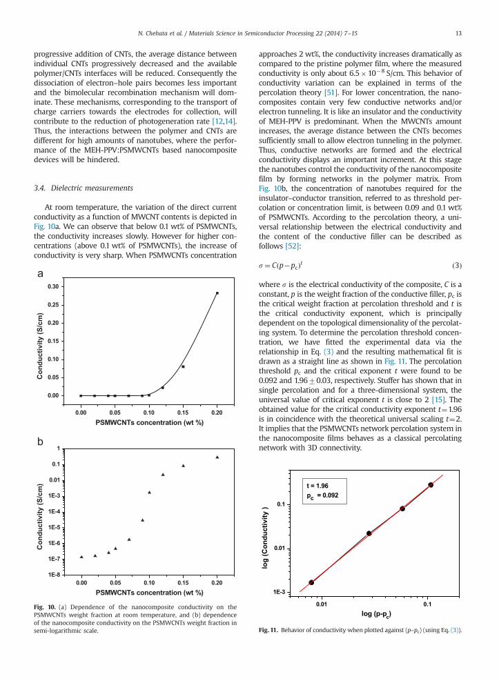
At room temperature, the variation of the direct currentconductivity as a function of MWCNT contents is depicted inFig. 10a. We can observe that below 0.1 wt% of PSMWCNTs,the conductivity increases slowly. However for higher con-centrations (above 0.1 wt% of PSMWCNTs), the increase ofconductivity is very sharp. When PSMWCNTs concentration
0.00 0.05 0.10 0.15 0.20
0.00
0.05
0.10
0.15
0.20
0.25
0.30
Con
duct
ivity
(S/c
m)
PSMWCNTs concentration (wt %)
0.00 0.05 0.10 0.15 0.201E-8
1E-7
1E-6
1E-5
1E-4
1E-3
0.01
0.1
1
Con
duct
ivity
(S/c
m)
PSMWCNTs concentration (wt %)
Fig. 10. (a) Dependence of the nanocomposite conductivity on thePSMWCNTs weight fraction at room temperature, and (b) dependenceof the nanocomposite conductivity on the PSMWCNTs weight fraction insemi-logarithmic scale.
approaches 2 wt%, the conductivity increases dramatically ascompared to the pristine polymer film, where the measuredconductivity is only about 6.5�10�8 S/cm. This behavior ofconductivity variation can be explained in terms of thepercolation theory [51]. For lower concentration, the nano-composites contain very few conductive networks and/orelectron tunneling. It is like an insulator and the conductivityof MEH-PPV is predominant. When the MWCNTs amountincreases, the average distance between the CNTs becomessufficiently small to allow electron tunneling in the polymer.Thus, conductive networks are formed and the electricalconductivity displays an important increment. At this stagethe nanotubes control the conductivity of the nanocompositefilm by forming networks in the polymer matrix. FromFig. 10b, the concentration of nanotubes required for theinsulator–conductor transition, referred to as threshold per-colation or concentration limit, is between 0.09 and 0.1 wt%of PSMWCNTs. According to the percolation theory, a uni-versal relationship between the electrical conductivity andthe content of the conductive filler can be described asfollows [52]:
s¼ Cðp�pcÞt ð3Þ
where s is the electrical conductivity of the composite, C is aconstant, p is the weight fraction of the conductive filler, pc isthe critical weight fraction at percolation threshold and t isthe critical conductivity exponent, which is principallydependent on the topological dimensionality of the percolat-ing system. To determine the percolation threshold concen-tration, we have fitted the experimental data via therelationship in Eq. (3) and the resulting mathematical fit isdrawn as a straight line as shown in Fig. 11. The percolationthreshold pc and the critical exponent t were found to be0.092 and 1.9670.03, respectively. Stuffer has shown that insingle percolation and for a three-dimensional system, theuniversal value of critical exponent t is close to 2 [15]. Theobtained value for the critical conductivity exponent t¼1.96is in coincidence with the theoretical universal scaling t¼2.It implies that the PSMWCNTs network percolation system inthe nanocomposite films behaves as a classical percolatingnetwork with 3D connectivity.
0.110.0
1E-3
0.01
0.1
log
(Con
duct
ivity
)
log (p-pc)
t = 1.96pc = 0.092
Fig. 11. Behavior of conductivity when plotted against (p–pc) (using Eq. (3)).

100 1000 10000 100000 1000000 1E71E-8
1E-7
1E-6
1E-5
1E-4
1E-3
0.01
0.1
10.2 wt %0.15 wt %0.12 wt %
0.05 wt %
0.09 wt %
0.07 wt %
0.1 wt %
0.04 wt %0.02 wt %
Con
duct
ivity
(S/c
m)
Frequency (Hz)
0 wt %
Fig. 12. The frequency dependence of AC conductivity for the MEH-PPV:PSMWCNT nanocomposites with different PSMWCNT contents at roomtemperature.
N. Chehata et al. / Materials Science in Semiconductor Processing 22 (2014) 7–1514
Fig. 12 shows a log–log plot of the frequency depen-dence of AC conductivity measured at room temperature,for nanocomposites with different contents of PSMWCNTs.With MWCNT contents lower than 0.09 wt%, the AC con-ductivity linearly increases with signal frequency. The ACconductivity plot, varying as a power of frequency (w),obeys to the power-law behavior described as follows [15]:
sACpws ð4Þwhere s denotes the critical exponent, following the inequal-ity 0rsr1and characterizing hopping conduction [53].
With increasing conductive filler amount, the plots reacha plateau at low frequencies, and the plateau starts to bendupward at higher frequencies and eventually becomesproportional to frequencies, showing the power-law beha-vior. For high concentration of PSMWCNTs (0.2 wt%), theconductance becomes independent of the frequency overthe entire frequency range and the power-law behavior isnot applicable for this conductive filler content and thenanocomposite behaves like a good conductor.
4. Conclusion
The effects of introducing different amounts of functio-nalized multi-wall carbon nanotubes (PSMWCNTs) in poly-mer solar cells have been investigated. The functionalizationprocess participates to ameliorate the dispersion of CNTs insolution and within polymer matrix, to yield homogenousorganic nanocomposites and ameliorate the quality ofobtained films. The transfer of photoinduced charges fromdonor polymer to acceptor nanotubes becomes efficient withthe increase in PSMWCNTs concentration, resulting in thedecrease of PL emission from the polymer. Under illumina-tion, the performance structure based on ITO/PEDOT:PSS/MEH-PPV:PSMWCNTs/Al shows an improvement with theprogressive incorporation of PSMWCNTs concentration,where the FF was 26% and 36% for MEH-PPV and MEH-PPV:PSMWCNTs (0.15 wt%), respectively. Further, the electri-cal conductivity of the composite films is found to increaserapidly with the increase in nanotubes content in the
solution beyond a threshold value. This behavior of conduc-tivity variation can be explained in terms of the percolationtheory. The results show that the conjugated polymer–CNTsnanocomposite represents an alternative way to manufac-ture organic photovoltaic cells with improved operation.
Acknowledgments
The authors gratefully acknowledge Prof. Joel Davenasfor his assistance in experiment work realized at PolymerEngineering Materials Laboratory, University of Lyon1,France.
References
[1] N. Yeh, P. Yeh, Renew. Sust. Energy Rev. 21 (2013) 421–431.[2] B. Parida, S. Iniyan, R. Goic, Renew. Sust. Energy Rev. 15 (2011)
1625–1636.[3] B.C. Thompson, J.M.J. Fréchet, Angew. Chem. Int. Ed. 47 (2008) 58–77.[4] C.J. Brabec, S. Gowrisanker, J.J.M. Halls, D. Laird, S. Jia, S.P. Williams,
Adv. Mater. 22 (2010) 3839–3856.[5] N. Asim, K. Sopian, S. Ahmadi, K. Saeedfar, M.A. Alghoul, O. Saadatian,
S.H. Zaidi, Renew. Sust. Energy Rev. 16 (2012) 5834–5847.[6] M. Helgesen, R. Søndergaard, F.C. Krebs, J. Mater. Chem. 20 (2010)
36–60.[7] Y.Y. Liang, Z. Xu, J.B. Xia, S.T. Tsai, Y. Wu, G. Li, C. Ray, L.P. Yu, Adv.
Mater. 22 (2010) 1–4.[8] F.C. Krebs, Sol. Energy Mater. Sol. Cells 93 (2009) 394–412.[9] B.A. Gregg, J. Phys. Chem. B 107 (2003) 4688–4698.
[10] S.A. Backer, K. Sivula, D.F. Kavulak, J.M.J. Frechet, J. Chem. Mater. 19(2007) 2927–2929.
[11] I. Khatri, S. Adhikari, H.R. Aryal, T. Soga, T. Jimbo, M. Umeno, Appl.Phys. Lett. 94 (2009) 093509–093511.
[12] J. Arranz-André, W.J. Blau, Carbon 46 (2008) 2067–2075.[13] A.J. Ferguson, J.L. Blackburn, N. Kopidakis, Mater. Lett. 90 (2013)
115–125.[14] Z. Liu, D. He, Y. Wangn, H. Wu, J. Wang, H. Wang, Sol. Energy Mater.
Sol. Cells 94 (2010) 2148–2153.[15] I. Singh, P.K. Bhatnagar, P.C. Mathur, I. Kaur, L.M. Bharadwaj,
R. Pandey, Carbon 46 (2008) 1141–1144.[16] J.Q. Wei, Y. Jia, Q.K. Shu, Z.Y. Gu, K.L. Wang, D.M. Zhuang, et al., Nano
Lett. 7 (2007) 2317–2321.[17] E. Kymakis, G.A.J. Amaratunga, Appl. Phys. Lett. 80 (2002) 112–114.[18] S.A. Curran, P.M. Ajayan, W.J. Blau, D.L. Carroll, J.N. Coleman,
A.B. Dalton, et al., Adv. Mater. 10 (1998) 1091–1093.[19] Y. Chen, R.C. Haddon, S. Fang, A.M. Rao, P.C. Eklund, W.H. Lee, et al., J.
Mater. Res. 13 (1998) 2423–2431.[20] W. Zhang, M.J. Yang, J. Mater. Sci. 39 (2004) 4921–4922.[21] L.M. Clayton, A.K. Sikder, A. Kumar, M. Cinke, M. Meyyappan,
T.G. Gerasimov, et al., Adv. Funct. Mater. 15 (2005) 101–106.[22] K. Lozano, E.V.J. Barrera, J. Appl. Polym. Sci. 79 (2001) 125–133.[23] C.A. Mitchell, J.L. Bahr, S. Arepalli, J.M. Tour, R. Krishnamoorti,
Macromolecules 35 (2002) 8825–8830.[24] J.L. Bahr, J.M. Tour, Chem. Mater. 13 (2001) 3823–3824.[25] C.A. Dyke, J.M. Tour, J. Am. Chem. Soc. 125 (2003) 1156–1157.[26] S. Qin, D. Qin, W.T. Ford, D.E. Resasco, J.E. Herrera, Macromolecules
37 (2004) 752–757.[27] A. Ltaief, A. Bouazizi, J. Davenas, P. Alcouffe, Thin Solid Films 516
(2008) 1578–1583.[28] S. Shao, K. Zheng, K. Zidek, P. Chabera, T. Pullerits, F. Zhang, Sol.
Energy Mater. Sol. Cells 118 (2013) 43–47.[29] ⟨http://www.graphistrength.fr⟩.[30] H. Ago, K. Petritsch, M.S.P. Shaffer, A.H. Windle, R.H. Friend, Adv.
Mater. 11 (1999) 1281–1285.[31] N. Chehata, A. Ltaief, A. Farzi, B. Ilahi, A. Bouazizi, Int. J. Nanotechnol.
10 (2013) 577–586.[32] Y. Zhao, G.X. Yuan, P. Roche, M. Leclerc, Polymer 36 (1995)
2211–2214.[33] J.J. Dittmer, E.A. Marseglia, R.H. Friend, Adv. Mater. 12 (2000)
1270–1274.[34] B. McCarthy, J.N. Coleman, R. Czerw, A.B. Dalton, M.I.H. Panhuis,
A. Maiti, et al., J. Phys. Chem. B 106 (2002) 2210–2216.

N. Chehata et al. / Materials Science in Semiconductor Processing 22 (2014) 7–15 15
[35] A.B. Dalton, J.N. Coleman, M.I.H. Panhuis, B. McCarthy, A. Drury, W.J. Blau, et al., J. Photochem. Photobiol. A: Chem. 144 (2001) 31–41.
[36] A.W. Musumeci, G.G. Silva, J.W. Liu, W.N. Martens, E.R. Waclawik,Polymer 48 (2007) 1667–1678.
[37] K.P. Ryan, S.M. Lipson, A. Drury, M. Cadek, M. Ruether,S.M. O'Flaherty, et al., Chem. Phys. Lett. 391 (2004) 329–333.
[38] B. McCarthy, J.N. Coleman, R. Czerw, A.B. Dalton, H.J. Byrne,D. Tekleab, et al., Nanotechnology 12 (2001) 187–190.
[39] A. Ltaief, A. Bouazizi, J. Davenas, R. Ben Chaabane, H. Ben Ouadaa,Synth. Met. 147 (2004) 261–266.
[40] Y. Shi, J. Liu, Y. Yang, J. Appl. Phys. 87 (2000) 4254–4263.[41] E. Kymakis, G.A.J. Amaratunga, Sol. Energy Mater. Sol. Cells 80 (2003)
465–472.[42] W. Lee, J. Lee, S.H. Lee, J. Chang, W. Yi, S.H. Han, J. Phys. Chem. C 111
(2007) 9110–9115.[43] N.S. Sariciftci, L. Smilowitz, A.J. Heeger, F. Wudl, Science 258 (1992)
1474–1476.[44] J. Geng, B.-S. Kong, S.B. Yang, S.C. Youn, S. Park, T. Joo, H.-T. Jung, Adv.
Funct. Mater. 18 (2008) 2659–2665.
[45] C.J. Collison, S. Pellizzeri, F. Ambrosio, J. Phys. Chem. B 113 (2009)5809–5815.
[46] O. Groning, O.M. Kuttel, C. Emmenegger, P. Groning, L. Schlapbach,J. Vac. Sci. Technol. B 18 (2000) 665–678.
[47] J.X. Geng, T.Y. Zeng, J. Am. Chem. Soc. 128 (2006) 16827–16833.[48] M.A. Ibrahim, H.K. Roth, U. Zhokhavets, G. Gobsch, S. Sensfuss, Sol.
Energy Mater. Sol. Cells 85 (2005) 13–20.[49] E. Kymakis, P. Servati, P. Tzanetakis, E. Koudoumas, N. Kornilios,
I. Rompogiannakis, Y. Franghiadakis, G.A.J. Amaratunga, Nanotech-nology 18 (2007) 435702–435707.
[50] K. Liu, S. Qu, X. Zhang, F. Tan, Z. Wang, Nanoscale Res. Lett. 8 (2013)88–93.
[51] G. Stauffer, London: Taylor & Francis; 1985.[52] I. Webman, J. Jortner, M.H. Cohen, Phys. Rev. B 16 (1977) 2593–2596.[53] A. Ltaief, A. Bouazizi, J. Davenas, P. Alcouffe, R. Ben Chaâbane, Thin
Solid Films 511–512 (2006) 498–505.