optical designs for improved solar cell performance
TRANSCRIPT

Optical Designs for Improved Solar Cell
Performance
Thesis byEmily Dell Kosten
In Partial Fulfillment of the Requirementsfor the Degree of
Doctor of Philosophy
California Institute of TechnologyPasadena, California
2014
(Defended May 15, 2014)

© 2014
Emily Dell Kosten
All Rights Reserved
ii

To Mom and Dad, who always encouraged my questions.

Acknowledgements
I am very grateful to the many people who helped make this thesis possible. Most
importantly, I was very fortunate to have Harry Atwater as my adviser. He was
endlessly supportive and enthusiastic, and his ideas and advice were crucial to much
of this work. In addition, Harry taught me so much about crafting a paper and
telling the story behind the science. Perhaps most importantly, though, the kind,
collaborative research group he established was a wonderful place to work for five
years.
The other students and post-docs in the Atwater group have been wonderful col-
laborators and friends. While I am very grateful to all of the folks who helped create
the friendly atmosphere in the group, there are many who require specific mention.
First, Greg Kimball taught me how to be a grad student during my first few months
in the group. I was also very fortunate to have Mike Deceglie, Adele Tamboli, Morgan
Putnam, Dennis Callahan, Matt Sheldon, Victor Brar, and Dagny Fleischman as my
officemates over the years. Mike, Adele, and Matt were very helpful as I was starting
out, and all my officemates provided lots of useful and fun discussion.
Later on, the full spectrum team, consisting of Matt Escarra, Cris Flowers, John
Lloyd, Sunita Darbe, Kelsey Whitesell, Michelle Dee, Carissa Eisler, and Emily War-
mann, became close collaborators as well as a lovely group of friends. I am particularly
grateful to John for his significant contributions to the light trapping filtered concen-
trator work, especially the ray tracing. Cris also provided significant Python help
which was crucial to automating the ray tracing work. Emily contributed substan-
tially to the light trapping filtered concentrator work with cell bandgap optimizations,
multijunction code, and detailed balance calculations. The advice and technical help
she provided with the GaAs experiments, particularly contacting, were crucial. I have
also very much enjoyed our chats over tea. In addition to our collaboration on the
full spectrum project, Carissa provided significant expertise with photoluminescence
measurements and sputtering, helpful discussion, and funny cat stories.
Jeff Bosco, Chris Chen, Naomi Coronel, Hal Emmer, Jim Fakonas, and Sam Wil-
iv

son all entered the group at the same time as I did. I have very much appreciated their
friendship and help over the years. In particular, Hal provided significant useful dis-
cussion on silicon solar cells, and Jeff and Sam were very helpful on device physics and
fabrication questions. Carrie Hoffmann, Vivian Ferry, Imogen Pryce, Stan Burgos,
Mike Kelzenberg, and Dan Turner-Evans provided significant mentorship and advice,
with particular assistance from Dan and Mike on the silicon microwires project. Car-
rie was also very helpful in her role as assistant director of the LMI-EFRC and adviser
to the full spectrum project, and provided the LaTeX template files for this thesis.
I’ve also appreciated technical help and discussions with Will Whitney, Ana Brown,
and Nick Batara.
Jennifer Blankenship, Tiffany Kimoto, Lyra Haas, and April Neidholdt provided
invaluable administrative support, as well as many enjoyable chats over the years.
Their help with the administrative side was crucial to my graduate school experi-
ence. Within the applied physics department, Christy Jenstad and Mabel Chik were
also very kind and helpful with purchasing and administration. Donna Driscoll, the
physics department coordinator, provided invaluable assistance as I navigated classes,
qualifying exams, candidacy, and finally the thesis and defense.
The other members of my committee, Michael Cross, Michael Roukes, and Keith
Schwab, have been generous with their time and feedback over the years. I’ve also
very much appreciated advice from Neil Fromer, about both science and broader ca-
reer questions. This work also benefited significantly from collaborators within the
LMI-EFRC, particularly Emily Warren in the Lewis group at Caltech, Owen Miller
in the Yablonovitch group at Berkeley, and Paul Braun and his group at UIUC. Col-
laboration with Albert Polman and his group at FOM AMOLF in Amsterdam has
also proved highly productive. Albert’s encouragement for my work on angle restric-
tion in silicon was particularly appreciated, as was assistance from Bonna Newman,
Piero Spinelli, and James Parsons in his group. Brendan Kayes at Alta Devices was
very generous with samples and advice, and his cells were crucial to the experimental
work in GaAs presented in this thesis. Finally, John Geisz, Myles Steiner, and Daniel
Friedman at NREL were helpful in discussing the details of GaAs cells, and providing
v

samples.
Beyond my work friends, I’ve also greatly enjoyed the wonderful group of friends
I’ve found in Pasadena. Emzo de los Santos, Branimir Cacic, Nate Glasser, Stephanie
Barnes, Greg Loos, Betty Wong, Emily Capra, and Jackson Cahn were always up for
boardgames, adventurous meals, and trivia, providing many a welcome break from
work. I’ve also been lucky enough to have several old and dear friends, Carolyn
Brennan, Katie Gose, and Leo Ungar, in Pasadena during graduate school, and it has
been wonderful to spend time with them on a regular basis.
Finally, I’d like to thank my family. My parents introduced me to science and
have always encouraged me. I’m very grateful for all their love, support, and interest
in my work. I always look forward to seeing and hearing from my sisters, Sarah and
Margaret. I really appreciate their love, and taking the time to visit and chat despite
their own busy lives. Finally, I’d like to thank my husband, Joe Zipkin. He has been
wonderfully helpful and loving through graduate school. I don’t know what I would
have done without his care and support. I love you so, honey, and I’m so grateful for
our little family of you, me, and the kitty.
Emily D. Kosten
May 2014
Pasadena, CA
vi

Abstract
The solar resource is the most abundant renewable resource on earth, yet it is currently
exploited with relatively low efficiencies. To make solar energy more affordable, we
can either reduce the cost of the cell or increase the efficiency with a similar cost cell.
In this thesis, we consider several different optical approaches to achieve these goals.
First, we consider a ray optical model for light trapping in silicon microwires. With
this approach, much less material can be used, allowing for a cost savings. We next
focus on reducing the escape of radiatively emitted and scattered light from the solar
cell. With this angle restriction approach, light can only enter and escape the cell near
normal incidence, allowing for thinner cells and higher efficiencies. In Auger-limited
GaAs, we find that efficiencies greater than 38% may be achievable, a significant
improvement over the current world record. To experimentally validate these results,
we use a Bragg stack to restrict the angles of emitted light. Our measurements show
an increase in voltage and a decrease in dark current, as less radiatively emitted
light escapes. While the results in GaAs are interesting as a proof of concept, GaAs
solar cells are not currently made on the production scale for terrestrial photovoltaic
applications. We therefore explore the application of angle restriction to silicon solar
cells. While our calculations show that Auger-limited cells give efficiency increases
of up to 3% absolute, we also find that current amorphous silicion-crystalline silicon
heterojunction with intrinsic thin layer (HIT) cells give significant efficiency gains
with angle restriction of up to 1% absolute. Thus, angle restriction has the potential
for unprecedented one sun efficiencies in GaAs, but also may be applicable to current
silicon solar cell technology. Finally, we consider spectrum splitting, where optics
direct light in different wavelength bands to solar cells with band gaps tuned to those
wavelengths. This approach has the potential for very high efficiencies, and excellent
annual power production. Using a light-trapping filtered concentrator approach, we
design filter elements and find an optimal design. Thus, this thesis explores silicon
microwires, angle restriction, and spectral splitting as different optical approaches for
improving the cost and efficiency of solar cells.
vii

Contents
List of Figures xii
List of Tables xv
1 Introduction 1
1.1 Motivation . . . . . . . . . . . . . . . . . . . . . . . . . . . . . . . . . 1
1.2 Solar Cell Fundamentals . . . . . . . . . . . . . . . . . . . . . . . . . 2
1.2.1 Solar Cell Structure . . . . . . . . . . . . . . . . . . . . . . . . 2
1.2.2 Current: Absorption and Carrier Collection . . . . . . . . . . 3
1.2.3 Current-Voltage Relationship . . . . . . . . . . . . . . . . . . 6
1.3 Optics Background . . . . . . . . . . . . . . . . . . . . . . . . . . . . 7
1.3.1 Ray Optics . . . . . . . . . . . . . . . . . . . . . . . . . . . . 7
1.3.2 Lambertian Light Trapping Surfaces . . . . . . . . . . . . . . 8
1.3.3 Interference-based Optical Coatings . . . . . . . . . . . . . . . 10
1.4 Overview of Thesis . . . . . . . . . . . . . . . . . . . . . . . . . . . . 11
2 Light Trapping in Silicon Microwires 13
2.1 Motivation . . . . . . . . . . . . . . . . . . . . . . . . . . . . . . . . . 13
2.2 Modeling Wire Array Intensity Enhancement under Isotropic Illumi-
nation . . . . . . . . . . . . . . . . . . . . . . . . . . . . . . . . . . . 14
2.2.1 Model Set-up: Balancing Fluxes . . . . . . . . . . . . . . . . . 14
2.2.2 Evaluation of Side Losses with a Radial Escape Approximation 18
2.2.3 Evaluating Side Absorption: Shadowing . . . . . . . . . . . . 20
viii

2.3 Results for Wire Array Intensity Enhancement under Isotropic Illumi-
nation . . . . . . . . . . . . . . . . . . . . . . . . . . . . . . . . . . . 21
2.4 Modeling Wire Array Intensity Enhancement with a Lambertian Back
Reflector . . . . . . . . . . . . . . . . . . . . . . . . . . . . . . . . . . 23
2.4.1 Governing Equation: Back Reflector Model . . . . . . . . . . . 23
2.4.2 Evaluating Side Loss with Reflector Scattering . . . . . . . . . 25
2.4.3 Evaluating Side Absorption with Reflector Scattering . . . . . 27
2.5 Results for Wire Array Intensity Enhancement with a Lambertian Back
Reflector . . . . . . . . . . . . . . . . . . . . . . . . . . . . . . . . . . 29
2.6 Comparison of Model with Experimental Data . . . . . . . . . . . . . 31
2.6.1 Including Absorption in Ray Optics Model . . . . . . . . . . . 31
2.6.2 Experimental Methods . . . . . . . . . . . . . . . . . . . . . . 32
2.6.3 Comparison of Model and Experiment: The Importance of
Wave Optical Effects . . . . . . . . . . . . . . . . . . . . . . . 33
2.7 Conclusions . . . . . . . . . . . . . . . . . . . . . . . . . . . . . . . . 35
3 Modeling the Effects of Angle Restriction 37
3.1 Angle Restriction and Photon Entropy . . . . . . . . . . . . . . . . . 37
3.2 Enhanced Light Trapping and Photon Recycling . . . . . . . . . . . . 40
3.3 Detailed Balance Models . . . . . . . . . . . . . . . . . . . . . . . . . 41
3.3.1 Cells in the Radiative Limit . . . . . . . . . . . . . . . . . . . 41
3.3.2 Accounting for Non-Radiative Losses . . . . . . . . . . . . . . 44
3.4 Absorptivity in Light Trapping and Planar Cells . . . . . . . . . . . . 45
3.4.1 Accounting for Modal Structure . . . . . . . . . . . . . . . . . 45
3.4.2 Absorption in a Light Trapping Cell with Non-Ideal Back Re-
flector . . . . . . . . . . . . . . . . . . . . . . . . . . . . . . . 46
3.4.3 Parasitic Absorption of Emitted Light in a Light Trapping Cell 48
3.4.4 Absorption in a Planar Cell . . . . . . . . . . . . . . . . . . . 49
4 Angle Restriction in GaAs Solar Cells 51
4.1 Motivation . . . . . . . . . . . . . . . . . . . . . . . . . . . . . . . . . 51
ix

4.2 Angle Restriction in a Light Trapping GaAs Cell: Limits to Efficiency 52
4.2.1 Cell in the Radiative Limit . . . . . . . . . . . . . . . . . . . . 52
4.2.2 Effect of Auger Recombination . . . . . . . . . . . . . . . . . 53
4.3 Ideal and Non-Ideal Back Reflectors for a Light Trapping Cell . . . . 55
4.3.1 Effect of a Non-Ideal Back Reflector . . . . . . . . . . . . . . . 55
4.3.2 Dielectric Mirrors Approaching Unity Reflectivity . . . . . . . 56
4.4 Comparison with a Planar Cell Geometry . . . . . . . . . . . . . . . 58
4.5 Comparison to Previous Work: The Radiative Efficiency Approach . . 58
4.6 Radiative Efficiency in Current GaAs Cell Technology . . . . . . . . . 62
4.7 Broadband Angle Restrictor Designs . . . . . . . . . . . . . . . . . . 63
4.8 Narrowband Angle Restrictor Design . . . . . . . . . . . . . . . . . . 67
4.9 Conclusions . . . . . . . . . . . . . . . . . . . . . . . . . . . . . . . . 75
5 Experimental Demonstration of Enhanced Photon Recycling in GaAs
Solar Cells 77
5.1 Motivation . . . . . . . . . . . . . . . . . . . . . . . . . . . . . . . . . 77
5.2 Narrowband Multilayer Angle Restrictor . . . . . . . . . . . . . . . . 79
5.3 Dark Current Measurements . . . . . . . . . . . . . . . . . . . . . . . 82
5.4 Voltage Enhancements Under Illumination . . . . . . . . . . . . . . . 84
5.5 Modified Detailed Balance Model . . . . . . . . . . . . . . . . . . . . 86
5.6 Variable Angle Restrictor Coupling . . . . . . . . . . . . . . . . . . . 89
5.7 Bandgap Raising and Angle Restriction Effects . . . . . . . . . . . . 92
5.8 Materials and Methods . . . . . . . . . . . . . . . . . . . . . . . . . . 92
5.8.1 Cell Contacting and Characterization . . . . . . . . . . . . . . 92
5.8.2 Optical Coupler Fabrication and Characterization . . . . . . . 93
5.8.3 Current-Voltage Measurements . . . . . . . . . . . . . . . . . 94
5.8.4 Implementation of the Modified Detailed Balance Model . . . 95
5.8.5 Gradual Coupling Measurements . . . . . . . . . . . . . . . . 96
5.9 Conclusions . . . . . . . . . . . . . . . . . . . . . . . . . . . . . . . . 96
x

6 Angle Restriction in Silicon Solar Cells 98
6.1 Motivation . . . . . . . . . . . . . . . . . . . . . . . . . . . . . . . . . 98
6.2 Effects of Angle Restriction in Ideal and Realistic Silicon Cells . . . . 101
6.2.1 Angle Restriction in Ideal Cells . . . . . . . . . . . . . . . . . 101
6.2.2 Angle Restriction in Realistic Cells . . . . . . . . . . . . . . . 103
6.2.3 Angle Restriction with External Concentration . . . . . . . . . 111
6.3 Angle Restrictor Designs . . . . . . . . . . . . . . . . . . . . . . . . . 114
6.3.1 Narrowband Angle Restrictor . . . . . . . . . . . . . . . . . . 115
6.3.2 Broadband Angle Restrictor . . . . . . . . . . . . . . . . . . . 117
6.4 Conclusions . . . . . . . . . . . . . . . . . . . . . . . . . . . . . . . . 120
7 Light-Trapping Filtered Concentrator For Spectral Splitting 122
7.1 Motivation . . . . . . . . . . . . . . . . . . . . . . . . . . . . . . . . . 122
7.2 The Light Trapping Filtered Concentrator . . . . . . . . . . . . . . . 126
7.3 Basic Design Considerations: The Multipass Model . . . . . . . . . . 127
7.3.1 The Thick Slab Assumption . . . . . . . . . . . . . . . . . . . 127
7.3.2 Initial Subcell Optimization . . . . . . . . . . . . . . . . . . . 131
7.3.3 Reducing Probability of Slab Escape: Design Tradeoffs . . . . 131
7.4 Designing Omnidirectional Filters . . . . . . . . . . . . . . . . . . . . 133
7.5 Optimizing Geometry and Filter Selection: Ray Trace Results . . . . 138
7.5.1 Filter Selection . . . . . . . . . . . . . . . . . . . . . . . . . . 138
7.5.2 Subcell Re-Optimization . . . . . . . . . . . . . . . . . . . . . 140
7.5.3 Angle Restrictor Geometry Optimization . . . . . . . . . . . . 143
7.6 Conclusions . . . . . . . . . . . . . . . . . . . . . . . . . . . . . . . . 144
8 Conclusions and Outlook 146
A Detailed Balance Code for GaAs 150
B Detailed Balance Code for Silicon 155
xi

List of Figures
1.1 Solar Cell Schematic: p-n Junction. . . . . . . . . . . . . . . . . . . . 2
1.2 Solar Cell Bandgap and Current . . . . . . . . . . . . . . . . . . . . . 4
1.3 Light Trapping and Planar Geometry . . . . . . . . . . . . . . . . . . 5
1.4 Current-Voltage Curve . . . . . . . . . . . . . . . . . . . . . . . . . . 6
1.5 The 2n2 Light Trapping Limit . . . . . . . . . . . . . . . . . . . . . . 9
1.6 Reflectivity of Periodic and Aperiodic Thin Film Multilayers . . . . . 10
2.1 Schematic: Microwire Array without Back Reflector . . . . . . . . . . 17
2.2 Light Trapping Factor Variation with Microwire Array Filling Fraction 22
2.3 Schematic: Microwire Array with Lambertian Back Reflector . . . . . 24
2.4 Variation of Power with Array Filing Fraction . . . . . . . . . . . . . 30
2.5 Comparison of Ray Optics Model to Experimental Absorption Mea-
surement . . . . . . . . . . . . . . . . . . . . . . . . . . . . . . . . . . 34
3.1 Photon Entropy Increase in a Conventional Solar Cell . . . . . . . . . 37
3.2 Photon Entropy in Concentrator and Angle Restrictor Systems . . . . 39
3.3 Light Trapping and Photon Recycling with Angle Restriction . . . . . 40
3.4 Balancing Photon Fluxes in the Detailed Balance Model . . . . . . . 42
4.1 Angle Restriction in a Light Trapping GaAs Cell . . . . . . . . . . . 54
4.2 Broadband Omnidirectional Dielectric Reflectors . . . . . . . . . . . . 57
4.3 Angle Restriction in a Planar GaAs Cell. . . . . . . . . . . . . . . . . 59
4.4 Angle Restriction and Cell Geometry: Radiative Efficiency Model . . 61
4.5 Broadband Angle Restrictor Designs . . . . . . . . . . . . . . . . . . 65
xii

4.6 Rugate Angle Restrictor Design . . . . . . . . . . . . . . . . . . . . . 69
4.7 Rugate Angle Restrictor Calculated Reflectivity . . . . . . . . . . . . 71
4.8 Current Effects of Rugate Design . . . . . . . . . . . . . . . . . . . . 72
4.9 Predicted Efficiency with Rugate Design . . . . . . . . . . . . . . . . 73
4.10 Predicted Efficiency with Rugate Design and Concentration . . . . . 74
5.1 Enhanced Photon Recycling in a Planar GaAs Cell . . . . . . . . . . 80
5.2 Narrowband Dielectric Angle Restrictor Design and Fabrication . . . 81
5.3 Dark Current Measurements and Fits . . . . . . . . . . . . . . . . . . 83
5.4 Voltage Increase with Current Losses . . . . . . . . . . . . . . . . . . 85
5.5 Voltage Increase with Equalized Currents . . . . . . . . . . . . . . . . 87
5.6 Loss of Emitted Light From Sides for Variable Coupling . . . . . . . . 90
5.7 Voltage Effects of Variable Angle Restrictor Coupling . . . . . . . . . 91
6.1 Angle Restriction in Silicon: Light Trapping . . . . . . . . . . . . . . 99
6.2 Effect of Angle Restriction in Auger Limited Silicon . . . . . . . . . . 104
6.3 Bulk Lifetime and Surface Recombination Estimation: IBC Cells . . . 107
6.4 Bulk Lifetime and Surface Recombination Estimation: HIT Cells . . . 108
6.5 Angle Restriction in HIT and IBC Cells . . . . . . . . . . . . . . . . 110
6.6 Effect of Bulk Lifetime, Back Reflectivity, and Surface Recombination
in Silicon Cells . . . . . . . . . . . . . . . . . . . . . . . . . . . . . . 112
6.7 Effect of External Concentration with Angle Restriction . . . . . . . . 114
6.8 Effect of Narrowband Angle Restrictor Design . . . . . . . . . . . . . 116
6.9 Effect of Broadband Angle Restrictor Design . . . . . . . . . . . . . . 119
7.1 Efficiency Increases with Many Solar Cell Junctions . . . . . . . . . . 124
7.2 Light-Trapping Filtered Concentrator . . . . . . . . . . . . . . . . . . 126
7.3 Monte-Carlo Model to Determine Dielectric Slab Thickness . . . . . . 128
7.4 Optical Efficiency with Multipass Model . . . . . . . . . . . . . . . . 129
7.5 Slab Probability of Escape: Acceptance Angle and Refractive Index . 132
7.6 Nearly Omnidirectional Long Pass Filter . . . . . . . . . . . . . . . . 134
xiii

7.7 Parasitic Loss and Transmission Trade-offs . . . . . . . . . . . . . . . 135
7.8 Varying Cutoff Wavelength . . . . . . . . . . . . . . . . . . . . . . . . 137
7.9 Reflectivity of Selected Filter Set . . . . . . . . . . . . . . . . . . . . 139
7.10 Photon Flux at Each Subcell . . . . . . . . . . . . . . . . . . . . . . . 142
7.11 Angle Restrictor Optimization Sweep . . . . . . . . . . . . . . . . . . 143
7.12 Variation of External Concentration . . . . . . . . . . . . . . . . . . . 144
xiv
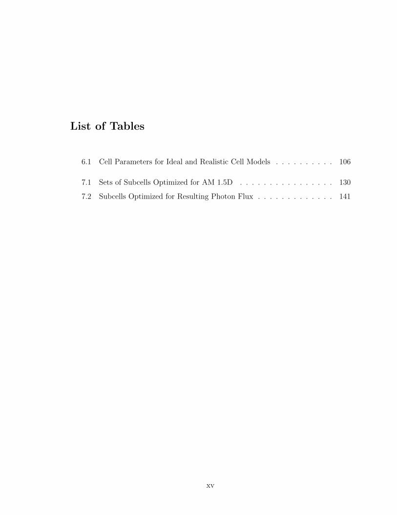
List of Tables
6.1 Cell Parameters for Ideal and Realistic Cell Models . . . . . . . . . . 106
7.1 Sets of Subcells Optimized for AM 1.5D . . . . . . . . . . . . . . . . 130
7.2 Subcells Optimized for Resulting Photon Flux . . . . . . . . . . . . . 141
xv

Portions of this thesis have been drawn from the following publications:
“Limiting Light Escape Angle in Silicon Photovoltaics: Ideal and Realistic Cells.”
E. D. Kosten, B. K. Newman, J. V. Lloyd, A. Polman and H. A. Atwater, in prepa-
ration.
“Experimental demonstration of enhanced photon recycling in angle-restricted GaAs
solar cells.” E. D. Kosten, B. M. Kayes, and H. A. Atwater, Energy & Environmental
Science 7, 1907-1912 (2014).
“Spectrum splitting photovoltaics: Light trapping filtered concentrator for ultrahigh
photovoltaic efficiency.” E. D. Kosten, J. Lloyd, E. Warmann and H. A. Atwater,
Proceedings of the 39th IEEE Photovoltaic Specialists Conference (PVSC) 3053-2057
(2013).
“Highly efficient GaAs solar cells by limiting light emission angle.” E. D. Kosten,
J. H. Atwater, J. Parsons, A. Polman, and H. A. Atwater, Light: Science & Applica-
tions 2, e45 (2013).
“Ray optical light trapping in silicon microwires: exceeding the 2n2 intensity limit.”
E. D. Kosten, E. L. Warren, and H. A. Atwater, Optics Express 19, 3316-3331 (2011).
xvi

Chapter 1
Introduction
1.1 Motivation
Solar energy is the world’s most abundant source of renewable energy. With an incom-
ing power of 1.2x10⁵ terawatts, the solar resource dwarfs current worldwide energy
consumption, estimated at 13 terawatts [1]. Despite the abundance of this renewable
resource, fossil fuels provide greater than 80% our energy [1]. While previously the
high cost of photovoltaics prevented more widespread adoption, recent developments
in the Chinese solar cell industry have greatly increased production and reduced price.
In fact, current module prices have allowed photovoltaics to achieve a levelized cost
of energy similar to coal and natural gas, though the long-term sustainability of such
prices is a matter of debate [2]. However, further cost reductions may yet be required
for solar energy to become a substantial part of the energy portfolio, as these cost
estimates do not include the storage necessitated by the intermittency of the solar
resource.
In reducing the cost of photovoltaic energy production, two approaches have been
pursued. The first has focused on novel materials, such as organic semiconductors,
quantum dots, and semiconductor nanowires, that could lead to cells that are sub-
stantially cheaper than current technologies but with somewhat lower efficiencies.
The silicon microwires discussed in Chapter 2 are an example of such an approach,
where the goal is to use microwires to reduce the cost of the cell significantly with
a relatively small reduction in efficiency relative to crystalline silicon solar cells. An
alternative approach is to improve the efficiency of the cell while attempting to min-
imize any associated cost increases. If efficiency can be increased without significant
1

increased cell cost, the cost per Watt will be reduced, as less cell area is required to
produce the same amount of power. Furthermore, “balance of systems” costs, such
as permitting, land, installation, and structural supports, are approximately half of
the cost of a photovoltaic installation [3]. As many of these costs scale with area,
improving cell efficiency also reduces balance of systems costs. With the exception of
Chapter 2, this thesis will focus primarily on increasing efficiency for high performing
cells as a means to reduce cost. The bulk of this thesis focuses on restricting the an-
gles of emitted light to improve efficiency in gallium arsenide (GaAs) and silicon solar
cells, two high performing materials. Finally, in the last chapter, we consider splitting
light into separate spectral bands to improve the efficiency of high performing III-V
solar cell materials.
1.2 Solar Cell Fundamentals
1.2.1 Solar Cell Structure!"#$%&'()**"+#&)+,&-"./0"1+&!2+#%$&
•! 31(&4"#$%&)501(*61+7&014)(&8244&9/0%&52&%$"8:2(&%$)+&%$2&)501(*61+&42+#%$;&
•! 31(&8)(("2(&81442861+7&014)(&8244&9/0%&52&%$"++2(&%$)+&%$2&,"./0"1+&42+#%$;&
•! '$/07&,"./0"1+&42+#%$&9/0%&52&#(2)%2(&%$)+&)501(*61+&42+#%$;&
<)+,",)8=&>?)9& >9"4=&-;&@10%2+& A&
p-type
n-type
photon
Figure 1.1. Photons are absorbed by a solar cell to generate electrons
and holes. These generated charge carriers are collected by a p-n
junction, as shown above, or by some other form of selective contact.
Solar cells made from inorganic semiconductors often consist of a p-n junction,
as shown in Figure 1.1. The basic concept is that incoming light is absorbed in
the semiconductor and the resulting electrons and holes are collected by the junction.
2

While Figure 1.1 illustrates a planar p-n junction, not all cells utilize such a geometry.
Furthermore, a p-n junction is not actually required, as all that is necessary are
selective contacts to collect the electrons and holes separately. In silicon cells with
an interdigitated back contact, for example, the bulk of the semiconductor has very
low doping, and alternating n-type and p-type heavily doped regions at the back of
the cell provide selective contacts to collect the electrons and holes respectively [4].
Finally, while many solar cells use homojunctions, where the selective contacts utilize
the same material as the primary cell absorber, heterojunctions may also be utilized,
where the selective contacts are formed from a different material than the primary
absorber. Some III-V cells utilize this approach, as well as HIT (heterojunction with
intrinsic thin-layer) silicon cells, where amorphous silicon is used to form the selective
contact [5, 6].
1.2.2 Current: Absorption and Carrier Collection
The absorption in a solar cell is determined by the semiconductor bandgap. As shown
in Figure 1.2, only photons with energy larger than the solar cell bandgap are absorbed
by the solar cell, which limits the efficiency. In addition, high energy photons in this
region are not utilized very efficiently, as the resulting carriers thermalize to the band
edge, and are collected at the same voltage as lower energy photons. The short circuit
current of a solar cell corresponds directly to the number of absorbed photons. Thus,
the limiting short circuit current is determined by the number of photons in the solar
spectrum that are above the band gap of the solar cell.
While the limiting short circuit current (Isc) is determined by the band gap and
solar spectrum, the actual short circuit current depends on how effectively the solar
cell absorbs the light above the bandgap. The absorptivity at a given wavelength is
determined by the path length of light within the solar cell, as well as the absorption
length of the semiconductor. Direct bandgap semiconductors, such as GaAs, have
short absorption lengths, and thus cells need only be a few microns thick to absorb
most of the incoming light. Indirect bandgap semiconductors, such as Si, have much
longer absorption lengths, and thus cells are on the order of 100 microns thick.
3

!"#$%&'(##&)$*+,*&
-&
!+&.$/01$2&
p-type
n-type !" '"/03,4"/&&
)$/0&
5$#(/,(&&
)$/0&
(6&
78&
•! 9.*"%.(0&27":"/*&1(/(%$:(&,$%%+(%*&
;7+,7&$%(&,"##(,:(0&.<&26/&=3/,4"/&
•! '$%%+(%*&>%"?&27":"/*&;+:7&(/(%1<&
1%($:(%&:7$/&:7(&.$/01$2&:7(%?$#+@(&
•! A7":"/*&;+:7&(/(%1<&#(**&:7$/&:7(&
.$/0&1$2&$%(&/":&$.*"%.(0&
Figure 1.2. Only photons with energy larger than the semiconductor
bandgap (shown in blue) are absorbed in the solar cell. This region is
marked in blue for silicon in the plot of the AM 1.5G solar spectrum
(below). Photons with energy above the band gap generate electron
hole pairs that thermalize (gray arrow) to the band edge. Thus, high
energy photons lose a substantial portion of their energy. Photons
with energy less than the band gap (shown in red) are not absorbed
in the semiconductor, and do not contribute to the solar cell current.
4

!"#$%&'()**"+#&)+,&-.((/+%&
-)+,",)01&23)4& 24"51&67&89:%/+& ;&
<:0&
=90&
&
&
&
-.((/+%&
=95%)#/&
&
&
&
<:0&
>5)+)(&?95)(&-/55&
!"#$%&'()**"+#&
?95)(&-/55&
!"#$%&%()**"+#&#"@/:&"+0(/):/,&:$9(%&0"(0."%&0.((/+%&
Figure 1.3. A light trapping geometry (top) enhances the light path
length and resulting absorption relative to a planar geometry (bot-
tom). Both cells have back reflectors.
Despite the thickness of current silicon cells, absorption is weak enough that light
trapping is required to enhance the path length of light within the cell. Using a
light trapping texture scatters the light, so it is trapped by total internal reflection,
as shown in Figure 1.3. As will be further discussed in Section 1.3.2, this offers
a significant path length enhancement relative to a planar cell. For direct bandgap
materials, dual pass absorption, as shown in Figure 1.3, is sufficient, and cells generally
utilize a planar geometry. A planar geometry also reduces surface recombination and
easily accommodates epitaxially grown window layers, which are crucial for high
quality III-V materials.
In a solar cell, it is key to collect the generated carriers, by either drift or diffusion,
before they recombine. Recombination can occur at bulk trap states, as in Shockley-
Read-Hall recombination, as well as at surfaces. These processes depend on the
quality of the solar cell material and surface passivation layers. In addition, two
intrinsic recombination processes occur within the bulk of the material. Radiative
recombination occurs when an electron and hole recombine to form a photon, and
is the inverse process to absorption. Auger recombination is a three particle process
involving either two electrons and a hole or two holes and an electron. The inverse
process to impact ionization, it involves the recombination of the electron hole pair
5

and the transfer of energy to the remaining carrier. This high energy carrier then
thermalizes to the band edge, ultimately producing heat.
1.2.3 Current-Voltage Relationship
At short circuit, all photogenerated carriers are collected before excess carrier pop-
ulation can build up within the cell. However, the excess carrier population within
the cell leads to the cell voltage, and thus there is no voltage or power production
at open circuit. At open circuit, in contrast, no carriers are collected, so the cell
does not generate current or power. At open circuit, the excess carrier population
and open circuit voltage (Voc) are determined by the balance between absorption and
recombination within the cell. (This will be discussed more fully in Chapter 3.) As
radiative recombination and absorption are set by the bandgap, Voc is generally 400-
500 mV lower than the bandgap for high quality cells. A larger Voc-bandgap offset
thus indicates that more non-radiative recombination is occurring in the cell.!"#$%&'(&)&*"+)%&,$++&
,)(-'-)./&01)2& 02'+/&34&5"67$(& 8&
96.&
:".&
!"#$%&!%"-;.'(<&=$<'"(&
&,;%%$(7&
:"+7)<$&
>?$%)@(<&&
!"'(7&
*"+)%&*?$.7%;2&
A"74&B%$)C!6;(&
*'&D)(-<)?&
Figure 1.4. A schematic current-voltage curve illustrates short cir-
cuit current, Isc, open circuit voltage, Voc, and the maximum power
point where the cell operates. The area of the power producing
region corresponds to the power produced at the operating point.
While the short and open circuit conditions provide valuable information about
6

absorption and recombination in the cell, neither produce any power. The shape of
the current-voltage relationship, or I-V curve, may be approximated as:
I(V ) ≈ Isc − IoeqV/kT (1.1)
where I is the current, V the voltage, Io the dark or recombination current, q the
electron charge, k the Boltzmann constant, and T the temperature. Because of the
exponential shape, a small reduction in voltage relative to Voc, allows for currents near
Isc, as is shown schematically in Figure 1.4. Thus, a voltage somewhat less than open
circuit allows for maximum power production in the cell. This voltage is known as the
maximum power or operating point, and the voltage is referred to as the operating
voltage (Vop) of the cell. The power generated by the cell at the operating point (Pop)
is then:
Pop = I(Vop)Vop = FFIscVoc (1.2)
where FF is the fill factor of the cell, or the area of the rectangle representing the
power producing region at the maximum power point divided by Isc,Voc product.
The fill-factor indicates how “square” the I-V curve is and increased series resistance
within the cell tends to degrade the fill-factor. The efficiency (η) of the cell is:
η =PopPsun
=FFIscVocPsun
(1.3)
where Psun is the power in the solar spectrum.
1.3 Optics Background
1.3.1 Ray Optics
Ray optics refers to the interaction of light with structures that are significantly larger
than the wavelength of light in the material. One rule of thumb is that the relevant
length scale of a structure should be at least ten times larger than the wavelength of
light in the material. This is very relevant when modeling the optics within solar cells.
7

For example, when modeling silicon solar cells, the largest wavelength of interest is
about 1100 nm, and the the refractive index is about 3.5. Thus, the wavelength of
light in the material is about 300 nm, and we can feel confident using ray optics
assumptions for cells where the minimum dimension is at least 3 µm.
For cells that are thinner than the ray optic limit, optical guided modes develop
within the thickness of the cell. These guided modes are based on the allowed solutions
to Maxwell’s equations, and more guided modes are present for thicker cells. Once
cells are in the ray optic limit, there are so many guided modes that they become a
continuum of optical states corresponding to angles of light that lie outside the escape
cone defined by total internal reflection. For cells thinner than the ray optic limit,
we must account for the finite number of guided modes in considering light trapping
within the cell. This will be discussed in more detail in Section 3.4.
For structures in the ray optic limit, ray tracing may be used to model the optical
properties. These simulations consist of starting a certain number of rays, and using
the Fresnel equations to follow their progress as they interact with various surfaces.
Receivers are used to detect the final location of each ray and determine the per-
formance. Both home-built and commercial ray trace software was utilized in this
work.
1.3.2 Lambertian Light Trapping Surfaces
When considering light trapping, Lambertian textured surfaces are often considered as
an ideal light trapping structure. These surfaces scatter light with equal brightness
in all directions, similar to a white sheet of paper. Alternatively, the intensity is
proportional to the cosine of the angle between the surface normal and the direction
of observation. For solar cells, Lambertian scattering leads to significant light trapping
benefits, including an approximately 50 times path length enhancment, for solar cells
in the ray optic limit [7].
To understand light trapping with a Lambertian surface, we assume that the solar
cell is not absorbing for purposes of calculating the intensity of light within the cell.
This is reasonable as light trapping is only important where light is weakly absorbed.
8

!"#$%&%$'()"*$!+,--(&)$'(.(*$
•! /,0,&1(&)$0()"*$(&$,&2$0()"*$34*5$&#)0#16&)$,783+-63&$
•! !#9*4+#2$:',.7#+6,&;$84+<,1#$81,=#+8$0()"*$
•! >&0?$@A%&%$3<$+,&23.(B#2$0()"*$#81,-#8$
•! C&*#+&,0$0()"*$(&*#&8(*?$D$%&%$E$(&1(2#&*$0()"*$(&*#&8(*?$
•! '()"*$*+,--(&)$<,1*3+$D$&%$F(*"34*$7,1G$+#H#1*3+$
$
$
IJK$K-+(&)$I##6&)$%L@@$ M.(0?$NO$P38*#&$ Q$
M81,-#$
R3&#$
MO$S,703&3T(*1"$,&2$UO$R32?O$!"""#$%&'()#"*+,)#-+./,+(5$!"#$%&:%;$:@VW%;O$
R,&2(2,1?$M9,.$
Figure 1.5. For a solar cell with a Lambertian back reflector, in-
coming light is scattered in all directions, but only light that is not
totally internally reflected and lies within the escape cone can leave
the cell. This leads to increased light intensity within the cell relative
to the intensity of incoming light.
Under the principles of detailed balance, at steady state in a non-absorbing material,
the light entering and escaping the material must balance. We assume an incoming
light intensity Iinc, and a light intensity within the cell of Iint. However, the escape
cone defined by total internal reflection allows only 1/2n2 of the light within the cell
to escape, where n is the cell index of refraction. Thus, for the outgoing and incoming
fluxes to balance:
Iinc =Iint2n2
(1.4)
and
Iint = 2n2Iinc (1.5)
This is known as the ergodic light trapping limit. For a solar cell without a back
reflector, the light intensity enhancement is n2 [7].
When weak absorption is included, the absorptivity of the cell, a, is:
a(E) =α(E)
α(E) + 14n2W
(1.6)
where E is the energy of light for which absorptivity is being evaluated, α is the
absorption coefficient, and W is the cell thickness. This can be understood intuitively
as the ratio of absorption to all sources of light loss, including absorption and light
9

escape. We also see a 4n2, or approximately 50 times, path length enhancement,
relative to a single pass through the cell. The additional factor of two relative to the
probability of light escape is due to enhanced path length from light at oblique angles
[7].
1.3.3 Interference-based Optical Coatings
In an optical thin film, interference occurs between light reflected at each interface,
and the patterns of constructive and destructive interference result in the reflectiv-
ity of the film. The simplest example is a single layer anti-reflective coating, where
destructive interference of reflected beams leads to enhanced transmission. The prin-
ciple is similar to impedance matching in electronics. With many alternating high
and low index layers in an optical coating, known as a Bragg stack, high reflectiv-
ity bands result from constructive interference of the reflections from each interface.
While Bragg stacks are traditionally periodic, introducing aperiodicity into a Bragg
stack can increase transmission around the reflecting band, as shown in Figure 1.6.
15 Emily Kosten [email protected] SPIE Optics and Photonics August 27th 2013
Aperiodic Dielectric Stack Filters
high index
low index
substrate
Aperiodicity allows additional design choices.
Stack filters may be omnidirectional with sufficient index
contrast and light incident from a low index material.
periodic
aperiodic
Figure 1.6. Optical multilayers with alternating high and low index
layers lead to high reflectivity bands. As these two reflectance spec-
tra show, introducing aperiodicity can increase transmission away
from the reflecting bands.
10

To produce the interference effect, each layer in the thin film will have a thick-
ness on the order of the wavelength of light. To model such structures, the transfer
matrix method is traditionally used. In this method, the propagation of the electric
field through each layer is represented by a matrix. The matrices for each layer are
then multiplied together, and the resulting matrix is used to determine the electric
field on either side of the optical multilayer, allowing the reflection and transmission
coefficients to be determined. Essentially, this method provides a simple formalism
for imposing the boundary conditions from Maxwell’s equations across each interface
in the multilayer.
1.4 Overview of Thesis
This thesis explores several problems related to optics and solar cells. In the second
chapter, we focus on light trapping in silicon microwires, developing a ray optical
model, and comparing to experimental measurements of absorption in the wires.
For the rest of the thesis we focus on very high quality cells performing near the
thermodynamic efficiency limits, and explore how optics can be utilized to further
increase the efficiency of such cells. The bulk of the thesis, Chapters 3-6, focuses
on utilizing optics that limit the angles at which light is emitted from a solar cell to
enhance efficiency. Using such optics both reduces the loss of radiatively emitted light,
and enhances light trapping for incoming light. In these chapters we introduce the
detailed balance model used to calculate the effects of angle restriction, and explore
the effects of angle restriction in both GaAs and Si for ideal and more realistic cells.
We also explore various optical structures that may be used to restrict the emission
angle and discuss a proof-of-concept experiment demonstrating the voltage benefits
to angle restriction. Finally, the last portion of the thesis, Chapter 7, focuses on
spectrum splitting, where external optics split the incoming light into spectral bands
of different energies. These spectral bands are then directed onto cells with bandgaps
tuned to the appropriate energy, thus reducing losses due to carrier thermalization
and lack of absorption. This chapter will discuss the benefits of spectrum splitting and
11

then focus on one particular optical design, the light-trapping filtered concentrator,
which applies many of the optical concepts discussed previously.
12

Chapter 2
Light Trapping in Silicon Microwires
2.1 Motivation
Silicon nanowire and microwire arrays have attracted significant interest as an alter-
native to traditional wafer-based technologies for solar cell applications [8-19]. Orig-
inally, this interest stemmed from the device physics advantages of a radial junction,
which allows for the decoupling of the absorption length from the carrier collection
length. In a planar cell, both of these lengths correspond to the thickness of the
cell, and high quality material is necessary so that the cell can absorb most of the
light while successfully collecting the carriers. In contrast, a radial junction offers the
possibility of using lower quality, lower cost materials without sacrificing performance
[12, 13]. More recently, such arrays have been found to exhibit significant light trap-
ping and absorption properties [8-10], and this absorption has been modeled in the
nanowire regime with a variety of wave optical models [15, 20-24].
As discussed previously, enhancing the light trapping and absorption within a
solar cell leads to an increase in short circuit current, and light trapping is particularly
important in silicon owing to the relatively low absorption in the material. Under
the light trapping limit for textured planar solar cells, known as the ergodic limit,
the intensity of light inside the solar cell is n2 times the intensity of light incident
upon the cell, or 2n2 for the case of a back-reflector, where n is the index of refraction
for the cell [7]. Some very recent experimental results have suggested that nano and
microwire arrays can exceed the ergodic limit [8, 9]. To explore this further, we
follow the approach used to derive the ergodic limit in the planar case to find the
expected light trapping and absorption for wires in the ray optics limit. This allows
13

us to compare to the ergodic limit and consider wires of a different scale than those
considered previously.
While much of the previous work has considered nanowires in the subwavelength
regime, far below the ray optics limit, large diameter microwires can be grown by
vapor-liquid-solid (VLS) techniques [8]. Previous device physics modeling suggests
that for efficient carrier collection wires should have diameters similar to the minority
carrier diffusion length, [13] and experimental measurements show diffusion lengths
for VLS grown microwires of 10 microns [25]. Because wires with such diameters
could approach the ray optics limit for solar wavelengths, it seems sensible to model
these structures in the ray optics regime. In addition, comparison of the ray optics
model with experimental data provides insight into the relative importance of wave
optics effects for wires of various diameters.
We begin by assuming there is no absorption in the wires and examine the case for
isotropic illumination so that we can compare to the ergodic light trapping limit for
textured, weakly absorbing solar cells with a traditional planar geometry. To make
this comparison, it is also necessary to postulate textured surfaces for the wires. We
then examine the case of wires on a Lambertian back reflector, which are illuminated
isotropically over the upper half sphere. Finally, we add a weak absorption term and
find the absorption as a function of wavelength and angle of incidence, allowing us to
compare with experimental data.
2.2 Modeling Wire Array Intensity Enhancement
under Isotropic Illumination
2.2.1 Model Set-up: Balancing Fluxes
We base our model on the principle of detailed balance, as was done to derive the
ergodic limit for textured planar sheets, discussed in Section 1.3.2 [7]. Under detailed
balance, in steady state the light escaping from the wires is set equal to the light
entering the wires. To illustrate our approach and show proof of concept for the model,
14

we first imagine a hexagonal array of wires suspended in free space and isotropically
illuminated. Furthermore, we assume that the wire surfaces are roughened such that
they act as Lambertian scatterers. In other words, the brightness of the wire surfaces
will be equal regardless of the angle of observation [26]. This fully randomizes the
light inside the wires in the limit of low absorption, just as the roughened surfaces of
planar solar cells do. The randomization of light within the wires serves to trap the
light inside by total internal reflection.
With these assumptions in mind, we find the governing equation by simply bal-
ancing the inflows and outflows of light within a single wire.
Iinc2AendTend + IincAsidesF =Iint2AendTend
n2+IintAsidesL
n2(2.1)
Above, Iinc is the intensity of the incident radiation, Iint is the the intensity of light
within the wires, Asides is the area of the wires sides, Aend is the area of one wire
end, and n is the index of refraction of the wire. In addition, Tend is the average
transmission factor through the end, L is light from the sides which escapes the
array, and F is the incident light which enters through the sides.
The terms on the left hand side represent the energy entering the wire array, with
the two terms representing the incident light which enters through the side and tops of
the wire, respectively. For the top of the wire, the calculation is quite simple because
there is no shadowing or multiple scattering, assuming that the wires are all the same
height. Thus, we need only average transmission into the top over the incident angles
to find Tend. For light entering through the sides, we take into account transmission
into the wire in addition to shadowing and multiple scattering. Thus, for a given
incident angle, we determine F , which gives the fraction of light transmitted through
the sides, averaged over the angles of the incident radiation.
On the right hand side, we have the energy outflows. Once again, the outflows
from the top are quite simple, as all light that leaves the top is lost to the array. The
factor of 1/n2 is due to total internal reflection of the randomized light inside the
wire, as Yablonovitch previously demonstrated for ergodic structures [7]. Due to the
15

isotropic incident radiation, the averaged transmission fractor Tend is the same for
incident and escaping light. For losses through the sides, much of the emitted light
will be transmitted into other wires, and not lost from the array. Thus, an average
loss factor, L, is found, which gives the side losses that are not transmitted into other
wires.
We rearrange the above equation to find the degree of light-trapping, or Iint/Iinc.
IintIinc
=n2(2AendTend + AsidesF )
2AendTend + AsidesL(2.2)
Note that in the limit where the area of the sides goes to zero, the light trapping
factor is n2, which reproduces the ergodic limit for a planar textured sheet that is
isotropically illuminated, as we expect. If F is larger than L, the light trapping in
this structure could exceed the ergodic limit. This seems unlikely, however, as time-
reversal invariance would suggest that L = F because each path into the array must
also be an equally efficient path out of the array. Furthermore, from a thermodynam-
ics perspective, we expect that the light trapping in this structure should be exactly
n2. This is because the equipartition theorem states that all the states or modes
should be equally occupied in thermodynamic equilibrium, and the density of states
within the wires is n3 the of states in free space. (When calculating the intensity,
it is necessary to multiply by the group velocity which goes as 1/n, such that the
intensity is increased by n2 [7].) Thus, this case will allow us to assess the accuracy
of the model and the assumptions necessary to simplify the calculation.
Averaging over all solid angles, with an appropriate intensity weighting, gives Tend:
Tend =
∫ 2π
0
∫ π/20
T (φ) cos(φ) sin(φ) dφ dθ∫ 2π
0
∫ π/20
cos(φ) sin(φ) dφ dθ=
∫ 2π
0
∫ π/20
Tn cos2(φ) sin(φ) dφ dθ∫ 2π
0
∫ π/20
cos(φ) sin(φ) dφ dθ=
2
3Tn
(2.3)
where φ is the angle of incidence and Tn is the transmission factor at normal incidence,
and where we have used the transmission factor associated with a Lambertian surface
(Tn cos(φ)) [26].
16

Figure 2.1. a) Schematic of the wire array for isotropic illumination.
The blue wires illustrate how light escaping from the side of a wire
impinges on a neighboring wire a given distance away. The orange
wires illustrate how the sides of the wires are shadowed by neighbor-
ing wires for a given distance and angle of incidence. b) A top-down
view of the wire array illustrates the radial escape approximation.
The arrows show the directions of light escape being considered, and
the yellow areas give the in-plane angle subtended by the neighbor-
ing wires, with the distinct shades indicating neighboring wires at
two distinct distances. The wires farther away will have greater loss
associated than the closer wires.
17

2.2.2 Evaluation of Side Losses with a Radial Escape Ap-
proximation
To calculate L, we determine the fraction of light, g, escaping from the sides of a given
wire that impinges on neighboring wires. Then we determine the transmission into
those neighboring wires and the effect of multiple scattering from neighboring wires.
To find g, we invoke a radial escape approximation where we treat each wire as if it
were a line extending upward from the plane of the array. This approximation will
be more accurate for low filling fraction arrays, because greater distance between the
wires means that neighboring wires will more closely approximate line sources. The
radial escape approximation serves to significantly simplify the treatment of the in-
plane shadowing. With this assumption, we only need to calculate the portion of the
in-plane angle that is subtended by wires at a given distance, and the losses associated
with each distance in order to find g. As Figure 2.1b illustrates, the in-plane angle
subtended by neighboring wires at a given distance is calculated geometrically.
The fraction of light that impinges on a wire a given distance away, f(h), is easily
calculated from geometrical arguments and the properties of Lambertian surfaces, as
Figure 2.1a illustrates. To simplify the calculation we ignore the increase in wire to
wire distance as the wires curve away from each other. As before, this approximation
will be more accurate for lower filling fractions, where the wires are farther apart and
this effect will be smaller.
f(h) =
∫ θT−θB
cos(θ)dθ∫ π/2−π/2 cos(θ)dθ
=sin(θT ) + sin(θB)
2(2.4)
To find g(d), we integrate f(h) over the height of the wire and normalize.
g(d) =
∫ l0
sin(θT ) + sin(θB)dh
2l=
√l2 + d2 − d
l(2.5)
Then g is an average of g(d) weighted by the angles subtended at each distance.
Naturally, not all of the light which strikes a neighboring wire will be transmitted
into the wire. As before, we calculate a transmission factor as a function of distance,
18

Tint(d), and take a weighted average to find the overall internal transmission factor,
Tint. Here, however, we must account for the curvature of the wire because this signif-
icantly affects the angle the transmitted light makes with the wire surface. Assuming
equal brightness for the allowed in-plane and out-of-plane angles, the expression for
Tint(d) is:
Tint(d) =
∫ l0
∫ θT−θB
∫ α2
−α1Tn cos2(φ)dαdθdl∫ l
0
∫ θT−θB
∫ α2
−α1cos(φ)dαdθdl
(2.6)
where the θ’s give the bounds of the out-of-plane angles, the α’s the bounds of the
in-plane angles, and φ is the overall angle made with the wire.
To find L we sum the losses in each pass through the wire array. For the first
pass through the wire array, 1− g of light which left the wire side is lost, because it
does not impinge on any of the other wires, and escapes. This is multiplied by Tend
because the light must leave the side of the wire before it can escape the array. On
the second pass, the losses, L2, are as follows:
L2 = Tendg(1− Tint)(1− g) (2.7)
This assumes that the reflected light has a uniform height distribution. In reality,
more of the light emitted from the sides of the wires will impinge on the middle
of the neighboring wire than either end, owing to the Lambertian distribution of
light from the emitting wire. Thus, this assumption will overestimate the losses on
succeeding passes through the array, but greatly reduces the computational intensity
of the calculation by allowing for a generalization of the losses on the ith pass through
the array as:
Li = Tend(g(1− Tint))i−1(1− g) (2.8)
This can easily be summed to give L.
L = Tend(1− g)∞∑n=0
(g(1− Tint))n =1− g
1− g(1− Tint)(2.9)
19

2.2.3 Evaluating Side Absorption: Shadowing
In calculating F , the main additional phenomenon we must address is shadowing.
As Figure 2.1a illustrates, the shadowing fraction, u, as a function of wire to wire
distance and angle of incidence is:
u(d, β) =l − sl
=d cot(β)
l(2.10)
We then take a weighted average over the angle subtended at each distance to find
u(β), and also find the transmission factor for the incoming light as a function of β
by averaging over all in-plane angles α.
T0(β) =
∫ π/2−π/2 Tn cos2(φ)dα∫ π/2−π/2 cos(φ)dα
(2.11)
As before, φ is the overall angle the incoming ray makes with the wire, which will
depend on both α and β. Finally, we modify the multiple scattering model because
light will only be reflected off the unshadowed portion of the wire, which will vary as
a function of β. For the losses on the first pass through the array:
L1(β) = u(β)(1− T0(β))(1− g1(β)) (2.12)
For i > 1,
Li(β) = (1− g)u(β)(1− T0(β))g1(β)(1− T1(β))[g(1− Tint)]i−2 (2.13)
where Li gives the losses on the ith bounce, as before, and T1 and g1 give the transmis-
sion and impingement factors associated with the light reflected from the unshadowed
portion of the wires. Summing to find the total losses:
Lt(β) = u(β)(1− T0(β))
(1− g1(β) +
(1− g)g1(β)(1− T1(β))
1− g(1− Tint)
)(2.14)
20

Thus, for a given angle, β, the amount of light which is transmitted into the wires,
F (β), accounting for multiple scattering and shadowing is:
F (β) = u(β)− Lt(β) (2.15)
Averaging over all the angles of incidence gives F .
F =
∫ 2π
0
∫ π/20
F (β) sin2(β)dβdη∫ 2π
0
∫ π/20
sin2(β)dβdη(2.16)
Above, η is the polar angle, sin(β)dβdη is the differential solid angle, and the addi-
tional factor of sine gives the change in intensity with angle of incidence.
2.3 Results for Wire Array Intensity Enhancement
under Isotropic Illumination
Inserting the expressions found above into Equation 2.2, we calculate the light trap-
ping factor across a range of areal filling fractions, the fraction of the array covered
by wires, for various wire aspect ratios. The results are given in Figure 2.2 and are
indicated by the curves labeled “no back reflector”. For very large filling fractions we
approach the ergodic limit, because the terms involving the wire sides become very
small. We also reproduce the ergodic limit for very low filling fractions, where the
radial escape approximation will be most accurate.1 In between the results fall below
the ergodic limit, likely because the side loss factor, L, is overestimated in the radial
escape approximation. Because we expect thermodynamically that the result should
be n2, this suggests that our approximations are reasonable, especially for low filling
fractions, which are more likely to be of experimental interest. We also note that our
1Our model very slightly exceeds the ergodic limit across all aspect ratios for the smallest filling
fraction. This is observed across aspect ratios, with no trend with increasing aspect ratios. The
maximum amount by which the ergodic limit is exceeded is approximately 1% and is likely due to
small inaccuracies in the model.
21

Figure 2.2. The variation of the light trapping factor, as a multiple
of n2, as a function of areal filling fraction, for various aspect ratios
(height/radius). n=3.53. Because we assume a cylindrical wire ge-
ometry, the maximum attainable packing fraction is approximately
90%, which corresponds to the sides of the wires touching each other.
The minimum filling fraction shown is 0.1%. Both cases approach
their respective ergodic limits (denoted by gray dashed lines) for
large filling fractions. The no back reflector case is also very close
to the ergodic limit for very small filling fractions where the radial
escape approximation is accurate. Parts a and b show the same data
plotted against a linear and log scale.
22

results are closer to the ergodic limit for smaller aspect ratios. This is likely because
the terms involving the wire sides are relatively smaller, and thus inaccuracies in those
terms, such as overestimating L, will have less impact. Thus, our approach reason-
ably approximates the result we expect from thermodynamics, and the inaccuracies
introduced by the radial escape approximation are well understood.
2.4 Modeling Wire Array Intensity Enhancement
with a Lambertian Back Reflector
2.4.1 Governing Equation: Back Reflector Model
We now investigate the effect of having a Lambertian back reflector with isotropic
illumination in the upper half-sphere. In this case, no light will enter or escape
through the bottom ends of the wires, which are covered by the back-reflector, and
light that strikes the reflector will be scattered. In the planar case, the ergodic light
trapping limit for such a geometry is 2n2, owing to the back reflector. Additionally, it
seems that this geometry would give optimal scattering, as can be understood by basic
physical arguments. Experimentally, it has been found that placing scatterers within
the wire array can, in combination with a back-reflector, improve the performance
of the array [8, 14]. This is because scatterers prevent light which is at normal or
nearly normal incidence from going between the wires and bouncing off a planar back-
reflector and out of the array. Imagine that we could place scatterers at any height
level within the wire array. The light that scatters upward from the scatterers near
the bottom of the array will be more likely to impinge on a wire, as Figure 2.3 shows.
For optimal scattering, then, the scatterers should be placed at the bottom of the
array. Since a Lambertian back reflector is similar to placing scatterers on a planar
back reflector, this geometry allows us to investigate an optimal scattering regime as
well as providing an interesting comparison to the planar case.
The governing equation for this case once again relies on detailed balance, as
23

Figure 2.3. A schematic of the Lambertian back reflector case. The
green wires show the effects of scatterers placed at different heights
within the array. Note that for the lower scatterer light from a
much smaller range of angles is able to escape. The purple wires
illustrate the light which bounces off the reflector at a given point r
that escapes between the surrounding wires. Between the red wires
the shadowing of the reflector for incident light at a given angle and
wires at a given distance is shown.
24

shown below.
IincAendTend + IincAsidesF ′ + IincAreflR′ =IintAendTend
2n2+IintAsidesL′
2n2(2.17)
The terms on the left give the light entering a wire, and the terms on the right give
the amount of light escaping. Note that a factor of 1/2n2 replaces the 1/n2 factor
because the back reflector doubles the intensity of the light within the wires [7]. In
addition, L and F are replaced with L′ and F ′, indicating that we need to account
for the Lambertian back reflector when calculating them. Finally, we note that there
is a term accounting for the light that initially falls between the wires and strikes the
reflector. R′ gives the fraction of the light which initially strikes the back reflector
that subsequently enters a wire, accounting for shadowing and multiple scattering.
With a one wire unit cell, Arefl, is simply the reflector area associated with a single
wire. As before, we rearrange the above equation to find the relative intensities inside
and outside the wire.
IintIinc
=2n2(AendTend + AsidesF ′ + AreflR′)
AendTend + AsidesL′(2.18)
Once again, in the limit of zero side area, the light trapping reduces to the planar
ergodic limit of 2n2, as expected.
2.4.2 Evaluating Side Loss with Reflector Scattering
To find the appropriate expressions for L′ we note that g and Tint will both be modified
by the back reflector. Therefore, using the modified values of these, g′ and T ′int, in
our previous multiple scattering model gives L′. To find g′, we tally the light lost.
Half of the losses from the non-reflector case remain, corresponding to the light that
escapes from the top. The other half of the non-reflector losses are multiplied by the
losses associated with light bouncing off the reflector and not striking a wire, Lrefl.
1− g′ = (1− g)/2 + (1− g)/2 ∗ Lrefl (2.19)
25

As Figure 2.3 illustrates, we consider two wires a distance d apart, and of height
l, with the light being reflected from a point r on the reflector. The fraction of light
which escapes at a given location on the reflector will be
L(r) =
∫ θT−θB
cos(θ)dθ∫ π/2−π/2 cos(θ)dθ
=sin(tan−1(r/l)) + sin(tan−1((d− r)/l))
2=
r√r2+l2
+ d−r√(d−r)2+l2
2
(2.20)
Summing the light coming from all points along the two neighboring wires and ac-
counting for the Lambertian nature of the wire surfaces, we find the intensity of light
at point r:
I(r) =
∫ l
0
cos(η1)dh+
∫ l
0
cos(η2)dh =
∫ l
0
r√r2 + h2
dh+
∫ l
0
d− r√(d− r)2 + h2
dh (2.21)
where η1 is the angle to the horizontal made by a ray escaping the wire at a height
h to strike the reflector at a point r, and η2 is the same quantity for the other wire.
Averaging over all the points between the two wires with the appropriate intensity
weighting gives:
Lrefl(d) =
∫ d0I(r)
[r√r2+l2
+ d−r√(d−r)2+l2
]dr
2∫ d
0I(r)dr
(2.22)
Lrefl(d) is inserted into Equation 2.19 to find g′(d). We then take a weighted average
of g′(d) with respect to the angle subtended at each distance to find g′.
To find T ′int we note that light which impinges without striking the back reflector
has a transmission factor which remains unchanged from the non-reflector case. Thus,
once the transmission factor for light which bounces off the back reflector is calculated,
these two transmission factors can be appropriately weighted together to give an
overall transmission factor.
The approach to finding the transmission factor for light that has bounced off
the back reflector is similar the the approach for finding the transmission factor for
incident side light. Thus, we take T0(β) (see Equation 2.11), and weight it by the
cosine dependence associated with the back reflector. Finally, we average over the
26

position along the reflector with a weighting to account for the varying intensity, as
shown below.
Trefl(d) =
∫ d0I(r)
(∫ π/2θT
∫ π/2−π/2 Tn cos(θ) cos2(φ)dαdθ +
∫ π/2θB
∫ π/2−π/2 Tn cos(θ) cos2(φ)dαdθ
)dr∫ d
0I(r)
(∫ π/2θT
∫ π/2−π/2 cos(φ) cos(θ)dαdθ +
∫ π/2θB
∫ π/2−π/2 cos(φ) cos(θ)dαdθ
)dr
(2.23)
Since g′−g is the additional light impingement which results from light which has
struck the back reflector, we find:
T ′int(d) =g(d)Tint(d) + (g′(d)− g(d))Trefl(d)
g′(2.24)
Then the overall T ′int is a weighted average with the in-plane angles subtended at each
distance. Finally, g′ and T ′int are used in place of their unprimed counterparts in the
multiple scattering model (see Equation 2.9) to find L′.
2.4.3 Evaluating Side Absorption with Reflector Scattering
To find F ′ we insert g′ and T ′int in the multiple scattering model in place of their
unprimed counterparts. However, as Equation 2.14 shows, we also need to find T ′1
and g′1. To find g′1 we estimate the impact of the reflector, R, using the following
expression:
R = (1− g1(d))− (1− g(d))/2 (2.25)
This estimates the amount of light that would be lost, but instead strikes the reflector.
Because the top part will always be shadowed last, we assume the losses from the top
are constant and equal (1 − g(d))/2. Thus, everything else will strike the reflector,
and we use our previous result for Lrefl to find the total losses, 1− g′1(d).
1− g′1(d) = R ∗ Lrefl + (1− g(d))/2 (2.26)
27

This allows us to modify the transmission factor:
T ′1(d) =T1(d)g1(d) + Trefl(d)(g′1(d)− g1(d))
g′1(d)(2.27)
Inserting all the primed quantities for their unprimed counterparts in the equation
for F and dividing by two to account for the hemispherical illumination gives F ′. Ob-
viously, the shadowing fraction, u, and the transmission factor prior to any reflection,
T0, are unchanged by the presence of the reflector since the sun is directly striking
the wire.
To find R′, we first determine the shadowing of the reflector as a function of wire
to wire distance and angle of incidence. From Figure 2.3, the shadowed fraction of
the reflector u(d, β) is:
u(d, β) =d− l tan(β)
d(2.28)
Taking a weighted average with respect to angle subtended at a given distance gives
u(β). We average over all β’s, including the differential solid angle and a weighting
for intensity, to find u.
u =
∫ π/20
u(β) sin(β) cos(β)dβ∫ π/20
sin(β) cos(β)dβ(2.29)
Next we develop a multiple scattering model. The losses from light that doesn’t
hit a wire after the initial reflection is Linc, which we find by averaging L(r) over the
unshadowed portion of the reflector at each distance, with appropriate weighting for
shadowing and the angle subtended at each distance. Tinc, the transmission of light
after initial reflection, is found in an exactly analogous manner. (1− Linc)(1− Tinc)
is reflected back into the array after bouncing once off the wire. From the previous
result, (1 − g′)/(1 − g′(1 − T ′int)) of this light will be lost. Thus, the total losses for
light that initially strikes the reflector are:
Ltot = Linc + (1− Linc)(1− Tinc)1− g′
1− g′(1− T ′int)(2.30)
28

Then,
R′ = (1− Ltot)u (2.31)
To find R′, we have approximated the the shadowing of the reflector using the closest
distance between two wires, leading to an overestimation of the shadowing impact,
which should be larger for high filling fractions. This is consistent with our use of the
closest distance between two wires for wire to wire shadowing and losses.
2.5 Results for Wire Array Intensity Enhancement
with a Lambertian Back Reflector
Inserting the terms derived above into Equation 2.18, we find the light trapping factor,
which is plotted as a function of filling fraction in Figure 2.2 by the curves labeled
“Lambertian back reflector”. The results closely approach the relevant ergodic limit
of 2n2 for large filling fractions as the terms involving the wire sides and the reflector
become very small. As in the no back reflector case, the light trapping factor falls
below the ergodic limit as the filling fraction is decreased from the maximum. It seems
likely that, as before, the overestimation of L in the radial escape approximation
for these filling fractions is at least partially responsible for the decrease. This is
supported by the trend in aspect ratios, which is similar to that for the no back
reflector case.
Interestingly, we see that for small filling fractions, the light trapping increases
asymptotically, significantly exceeding the ergodic limit, in contrast to the no back
reflector case. As we previously noted, our approximations improve with decreasing
filling fractions. Thus, there is no reason to suspect that surpassing the ergodic limit
is an artifact of the modeling assumptions. Furthermore, we can understand the ob-
served asymptotic increase physically by considering the limit of small filling fraction.
For very small filling fractions, the side loss factor, L′, and the side transmission fac-
tor, F ′, are nearly constant, as they have nearly reached their maxima. In addition,
the radius is rapidly approaching zero. Thus, all the terms in Equation 2.18, with the
29

exception of the back reflector term, are decreasing as the square of the radius. How-
ever, the reflector area remains nearly constant with decreasing filling fraction, as the
array is already almost entirely reflector. Thus, if R′ is decreasing less quickly than
the radius squared, we should see asymptotic increase. In fact, fitting the asymptotic
regions of each of the curves, we find that the curves are increasing as r−p, where p
has values between 0.33 and 0.37. Figure 2.4 uses the fit in the calculation of the
power to give a sense of the goodness of the fit. The fits are quite good across all the
curves, and the values of p do not trend with aspect ratio. These fits suggests that
the back reflector transmission goes approximately as the radius to the 5/3 power in
the low filling fraction regime, across the range of aspect ratios explored here. The
variation of the onset of asymptotic behavior with aspect ratio is also consistent with
this explanation, as the denominator of the light trapping factor will decrease more
rapidly for shorter wires.
Figure 2.4. The variation of power with filling fraction, for aspect
ratio=50. The dotted lines use the asymptotic fits across all filling
fractions, so that the goodness of fit can be evaluated. The solid lines
use the model results across all filling fractions. Note that while the
asymptotic increase produces increased power per volume of silicon,
it does not produce increased power per unit area in the array.
To explore this further, we evaluated the relative power, per unit area and per unit
30

volume of silicon, for an array with an aspect ratio of 50. We assume constant solar cell
fill factor2 with increasing filling fraction, and assume that the short circuit current is
proportional to the volume and the light trapping factor. For an axial junction, the
open circuit voltage is proportional to ln(Jsc/J0), where Jsc is the short circuit current
density and J0 is the saturation current. We assume that for a light trapping factor of
2n2 the short circuit current density is 30 mA/cm2 and the saturation current density
is 10−12 A/cm2. As Figure 2.4 illustrates, while the asymptotic increase does produce
an increase in power per unit volume of silicon, as we expect, it does not produce an
increase in the power per unit area. This is because the reduced volume of silicon
per unit area leads to a reduced short circuit current, which is not overcome by the
relatively small increase in open circuit voltage. Thus, in some sense, the Lambertian
back reflector is acting as a concentrator, leading to increased power per unit volume
of silicon at the cost of power per unit area.
2.6 Comparison of Model with Experimental Data
2.6.1 Including Absorption in Ray Optics Model
Absorption measurements have been reported as a function of angle of incidence and
wavelenth for VLS-grown microwire arrays [8]. We therefore calculate the absorption
for such an array in the ray optics limit. This will give us insight as to the importance
of wave optic effects, and will allow us to determine the accuracy of the model for
arrays at various scales. We consider an array embedded in PDMS, with a quartz
slide underneath it. This very similar to the non-reflector case, except for the fact
that we have PDMS/quartz (n=1.4) instead of free space. In addition, we include
an absorption term in the governing equation. As Yablonovitch has shown, this term
should be equal to 2αV Iint, where α is the absorption coefficient, and V is the volume
2This should not be confused with the areal filling fraction of the wire array. As mentioned
previously, in solar cells the power can be calculated by multiplying the short circuit current, the
open circuit voltage, and the fill factor, where the fill factor accounts for the fact that the current-
voltage curve is not square in the power-producing region.
31

where the absorption is occurring [7].
Thus, the governing equation for a given angle of incidence θ, is:
A′sidesImax sin(θ)F (θ) + 2AendImax cos(θ)T (θ) = 2αV Iint +2AendTendIint
n2+AsidesLIint
n2
(2.32)
where Imax is the intensity of the incident light at normal incidence, and the factors
of sin(θ) and cos(θ), account for the decreased intensity at non-normal incidence.
Note that for the light entering through the sides we have A′sides instead a Asides, to
denote that we need to account for decreased intensity as the wire turns away from
the in-plane direction from which the light enters. Rearranging to find Iint gives:
Iint =A′sidesImax sin(θ)F (θ) + 2AendImax cos(θ)T (θ)
2αV + 2AendTendn2 + AsidesL
n2
(2.33)
The fraction of light absorbed, A, is:
A =2αV Iint
AtotImax cos(θ)=
2αV (A′sidesF (θ) tan(θ) + 2AendT (θ))
Atot(2αV + 2AendTendn2 + AsidesL
n2 )(2.34)
where Atot is the total area of one unit cell. With the exception of A′sides, these terms
follow directly from our previous work. However, between various in plane angles, the
amount of shadowing will vary. Previously, to find F we averaged this over all the
in-plane angles. Experimentally, though, the light will only come from one in-plane
direction, which in this case was aligned in the direction of maximal shadowing. In
addition, to account for a non-free space medium, all the factors of 1/n2 are replaced
with n21/n
22, where n1 is the index of the embedding medium and n2 is the index of
the wires, due to the relative density of modes between the two media.
2.6.2 Experimental Methods
To find the experimental absorption data, arrays of silicon microwires were grown by
the VLS mechanism from SiCl4 precursors as reported previously [27]. The geometry
of the arrays was defined by the photolithographic mask used to pattern the VLS
32

catalyst islands. Wires with a radius of 1µm were grown from a hexagonally packed
mask with 3 µm diameter holes with a center to center spacing of 9 µm. Larger wires
with a radius of approximately 4 µm were grown from a hexagonally packed mask
with 15 µm diameter holes and 30 µm center to center spacing.
After growth, the metal VLS catalyst was removed from the wires and the height
and diameter of the wires were measured using scanning electron microscopy. The
wires were embedded in polydimethylsiloxane (PDMS, Sylgard) as reported previ-
ously [27]. The PDMS was dropcast onto the wires and spun at 3000 rpm, and then
cured at 120 C for 30 minutes. Wires were removed from the substrate by scraping
the PDMS film with a razor blade. Integrated reflection and transmission measure-
ments were performed with a custom-built 4 inch integrating sphere apparatus using
a Fianium supercontinuum laser illumination source and a 0.25 m monochromator
[8]. The absorption of each sample was determined from the wavelength and angle
resolved transmission and reflection measurements [13].
We then input structural parameters, as determined by SEM, from these measured
arrays into the model developed above. The PDMS embedding material was included
in the model, but the PDMS/air interface was neglected. (The PDMS/air interface
gives about 3% reflection.) For each angle of incidence and wavelength we found the
various absorption and loss terms, using wavelength specific n and α data. For wires
with an approximately 1µm radius, results are given in Figure 2.5a and b. We also
compare to wires with a radius of approximately 4µm and a similar aspect ratio,
which should be closer to the ray optics limit. The results are shown in 2.5c and d.
2.6.3 Comparison of Model and Experiment: The Impor-
tance of Wave Optical Effects
We found that the results for the larger wires are much more similar to the experimen-
tal data, though there is still significant disagreement. This suggests that there are
significant wave optics effects in the 1µm radius case, which become less significant for
the 4µm array. For example, if we examine the maximal absorption at near normal
33

Figure 2.5. a)The outlined surface gives the model output for wires
with a 4.9% filling fraction, a 1 µm radius, and a height of 44 µm.
The upper surface is the experimental result for such an array. b)
The solid lines show the experimental data for various wavelengths,
and the dotted lines show the model output. Note that even for the
low absorbing 1000 nm curves, the model significantly underpredicts
the absorption. c) The outlined surface gives the model output for
wires with a 7.3% filling fraction, a 4 µm radius, and a height of 160
µm. The other surface is the experimental result for such an array.
d) As before, the solid lines show the experimental data and the
dotted lines show the model output. Note the reasonable agreement,
especially at 1000nm.
34

incidence, we see that the model produces values similar to the filling fractions, and
the 4µm array gives a value fairly close to the filling fraction, with 11% absorption
for a 7% filling fraction. However, for the 1µm array we see 23% absorption for a 5%
filling fraction, suggesting a significant wave optic effect in this regime. In fact, it is
well known that particles on the order of the wavelength of light can have scattering
and absorption cross sections considerably larger than their physical size, whereas in
ray optics the cross section corresponds to the physical size [28]. It seems likely that
this effect is causing the enhanced absorption observed in the smaller wires.
Despite the reasonable agreement for angles of incidence relatively near normal,
the ray optics model fails to capture the strong increase in absorption observed with
large angles of incidence for wavelengths where the absorption is strong. However,
our model assumes that the light is fully randomized before any significant absorption
takes place, which will not occur in strongly absorbing wavelength regimes. Thus,
it is not surprising that our model fails to explain this behavior. As we expect,
the agreement is improved for wavelengths where the absorption is low and this
randomization condition is more accurate, as is shown in Figure 2.5d. However, even
in this case, the shape of the curve is not captured particularly accurately, most likely
due to differences between the experimental and modeled wires. For example, if the
experimental wire surfaces were not perfectly Lambertian, but somewhat specular,
the angular profile would likely be sloped across a wider range of angles, as is seen
here. This is because the light which strikes the wire sides would reflect in one
direction rather than be scattered in all directions, so light at near normal incidence
would be less likely to enter the sides than for specular wires. Thus, our model works
reasonably well in the low absorbing ray optics regime, but does not quite capture
the angular dependence, perhaps due to non-Lambertian experimental wire surfaces.
2.7 Conclusions
The model developed in this paper addresses wire geometries from a ray optics per-
spective, assuming Lambertian surfaces and weak absorption. In the non-reflector
35

case, the model produces light trapping close to the ergodic limit of n2 for filling
fractions approaching zero and approaching unity. This conforms with our thermo-
dynamic expectation and allows us to understand the accuracy of the approximations
used for computational feasibility. In addition, it confirms our physical expectations
about the regimes for which the approximations will be most accurate.
Applying the model to the case of a Lambertian back reflector, we observe signifi-
cant intensity enhancements, including asymptotic increases for small filling fractions
that significantly exceed the ergodic limit of 2n2. Quantitatively, for a filling frac-
tion of 0.1%, the enhancement can exceed 3n2, and the asymptotic increase goes
approximately as r−1/3, where r is the wire radius. These asymptotic increases result
from the reflector acting as a concentrator. Fitting these results gives insight into
the asymptotic behavior of the transmission factor for light that initially strikes the
reflector, which goes as approximately r5/3. It seems that a more sophisticated back
reflector, which preferentially scattered light sideways, could allow for asymptotic
behavior which would be even more dramatic, a topic that deserves further study.
However, while the asymptotic increases found here do give increased power per vol-
ume of silicon, there is reduced power per unit wire array area, owing to reduced
silicon volume at low filling fractions.
Finally, in comparing the model with experimental absorption data, there is agree-
ment with experiment for large (4 µm radius) wires in the low absorbing regime where
the model is valid. The results suggest that the very strong absorption observed in
smaller wires (1 µm radius) may be significantly due to wave optical effects, and
analysis using a wave optics formalism is required in order to understand this strong
absorption. Thus, even though previous modeling has suggested that large wires
could be superior from a device physics perspective, they appear to be less optimal
from a light trapping perspective. This trade-off deserves further study, as do the
wave optics effects observed in smaller wires.
36

Chapter 3
Modeling the Effects of Angle Restriction
3.1 Angle Restriction and Photon Entropy
Under direct sunlight, conventional solar cells emit light isotropically, while receiving
light only from the angles spanned by the solar disk, as shown in Figure 3.1. This
increase in the angular distribution of light corresponds to an increase in the photon
entropy, and the inherent entropy increase reduces the solar cell efficiency [29-32].
Thus, efficiency may be increased by reducing the angular spread of emitted light
!"#$%&'(&)*+,-.&
&
/01'&2*34*356*.&7-"#.53&&
8-93:53%&;<=&;>?@&
&
&
A#"#6.B&!"#++#*.&0.B$-&C*3&D"43*E-F&
7*$53&2-$$&G-3C*3"5.H-&
Figure 3.1. In a conventional solar cell under direct sunlight, light
is received from a narrow angular range but emitted from the cell
into a wide angular range, resulting in a photon entropy increase
and associated efficiency reduction. Here, the sun is illustrated at
normal incidence to the solar cell, as we assume a tracking system.
37

from the solar power conversion system.
Figure 3.2 illustrates two possible approaches to reducing the photon entropy in-
crease. Most commonly, concentrating solar systems partially exploit this angular
photon entropy term by redirecting the solar cell light emission into a narrow an-
gular range, as shown in Figure 3.2a. As is well known from deployed systems and
experimental measurements of solar cells under concentration, this leads to efficiency
increases at low to moderate concentration ratios, due to increases in the solar cell
voltage. While higher concentration ratios further reduce the angular spread of emit-
ted light and resulting photon entropy increase, they do not practically realize the
further efficiency gains that would be expected. At high concentration and the re-
sulting high current densities, increased series resistance and heating degrade the cell
efficiency, so that maximum efficiencies are achieved around a few hundred suns for
typical high concentration cells, rather than the approximately 46,000 suns possible
at maximum solar concentration [33-35].
While concentration has been employed with significant success, the heating and
series resistance losses mentioned earlier limit the possible benefits of photon entropy
management. With angle restriction, as shown in Figure 3.2b, an optic is placed above
the cell that allows light to enter or leave the cell only near normal incidence. Thus,
light that would otherwise be emitted at oblique angles is reflected back into the cell, a
process known as photon recycling [32]. Since cells with angle restriction operate with
current densities similar to traditional flat plate cells, heating and series resistance
do not contribute additional losses, and efficiencies above 40% are predicted in ideal
systems [31, 32]. However, while concentration has been implemented in commercial
systems, until recently it was thought that the benefits of angle restriction and photon
recycling would not be observable in experimental solar cells, owing to non-radiative
recombination [32].
38

!"
#"
Figure 3.2. a) A concentrator system takes the light emitted from all
angles in a solar cell and reflects it to within a narrow range of angles.
As concentration ratio increases, the emission angle from the concen-
trator is reduced, so to fully reduce the angle of emission, maximum
concentration is required. b) We propose a design for a thin coupler
which limits the emission angle without concentrating. This avoids
the deleterious heating and series resistance effects observed in high
concentration solar systems. Key to achieving the highest possible
efficiencies with design are the thin cell and the highly reflective,
light trapping back reflector shown in the schematic.
39

3.2 Enhanced Light Trapping and Photon Recy-
clingBenefits of Angle Restriction
!"#$%&'()**#%+,#-"."#/0))+"#!"""#$%&'()#*'#"+,-)#.,/)#1234456473648#9:8;<="#
#
#
Scattered incoming light is less
likely to escape, leading to
longer path length and more
absorption in a thinner cell
#
#
#
Light Trapping Photon Recycling
Light emitted via radiative
recombination is less likely to
escape and more likely to be
re-absorbed
."#-%0>#)?"#%*"#0)#122+)#345()#;69;=#7@<A37@AB#9:88A="#
#
#
Escape angles
without coupler
Solar Cell
Angle Restriction Optic
Textured Back Reflector
Emitted Light
Incoming Light
1&C*D#2"#EFG?)+#H#.?I%?)0#/0FJ'#
Figure 3.3. With angle restriction, the escape cone within the cell
is narrowed. The dotted lines illustrate the escape cone and corre-
sponding range of emitted angles without angle restriction, and the
solid lines indicate the escape cone and emitted angles under angle
restriction. The narrowed escape cone leads to enhanced light trap-
ping of incoming light (left), as well as enhanced photon recycling
of emitted light (right).
In a more mechanistic picture, the benefits to angle restriction are due to a nar-
rowed escape cone. As shown in Figure 3.3, total internal reflection in a non-angle
restricted cell leads to an escape cone of 16. With angle restriction, this escape
cone and the angular range of emission are both narrowed. This leads to enhance-
ments in both light trapping and photon recycling as it is more difficult for both
emitted and scattered light to escape. Enhanced light trapping occurs only in a cell
with a randomizing surface. (Such cells will be referred to as “light trapping” cells,
while cells without a randomizing surface will be referred to as “planar”.) Incoming
light is scattered by the randomizing surface, and the narrower escape cone leads to
an enhanced path length inside the the cell. This modifies our previous expression
40

(Equation 1.6) for the absorptivity in a light trapping cell:
a(E) =α(E)
α(E) + sin2(θ)4n2W
(3.1)
where θ is the emission angle of the solar cell [7, 30, 36]. Note that this expres-
sion reproduces Equation 1.6 where there is no angle restriction (θ = 90). Most
importantly, angle restriction allows for full light absorption in a thinner cell.
Enhanced photon recycling occurs because radiatively emitted photons that would
otherwise leave the cell are reflected back by the narrowed escape cone. Thus, ra-
diatively emitted photons are more likely to be re-absorbed and losses from radiative
recombination are reduced, leading to an increase in voltage. Note that enhanced
photon recycling can occur in either a light trapping or planar geometry, as radia-
tive emission occurs in all directions, randomizing the emitted light. However, the
benefits of enhanced photon recycling will only be significant for materials where ra-
diative recombination and emission is a major loss mechanism, like GaAs or other
III-V materials. In silicon, where non-radiative processes like Auger recombination
limit the voltage, enhanced photon recycling has little effect on efficiency. Instead, as
enhanced light trapping allows for full absorption in a thinner cell, losses from bulk
non-radiative processes are reduced, with a resulting increase in voltage and efficiency.
3.3 Detailed Balance Models
3.3.1 Cells in the Radiative Limit
To model the effects of angle restriction, we implement a detailed balance model,
originally developed by Shockley and Queisser [29]. In modeling angle restriction with
GaAs, detailed balance allows us to account for photon recycling effects, which are not
routinely included in device physics solar cell models. As in previous work, we initially
assume that all recombination is radiative, known as the radiative limit [29, 32, 36].
While this may seem unrealistic in a real cell, experimental GaAs cells have recently
come within a few percentage points of the detailed balance efficiency, and have
41

also achieved high external radiative efficiency1 (ERE) values, indicating that they
are approaching the radiative limit [37, 39]. Detailed balance also assumes that
each photon absorbed above the bandgap produces a single electron hole pair, which
immediately thermalizes to the solar cell bandgap [29]. Because of the thermalization
energy loss, the model balances photon number flux, rather than energy flux.
Detailed Balance Model: Concept
Semiconductor at open circuit. Assume only radiative recombination.
In steady state photons in (absorbed) must equal photons out (emitted).
!"#$#%&'()*+(,'
-.//',*0(12#%&3'
'
Carrier population at steady state determines open circuit voltage.
GaAs cells have achieved 48.5% external radiative efficiency (ERE).
4)*/5'67'8#&$(%'9':$;.$(0'<0#=>'
?7@7'8.5(&'($7'./7'!"#$%&#'&()*+&,---&!./0%&-ABCC3D'@7:7'E$(*%(0'($7'./7'1%&2334%&!+56%&-ABCF3''
@7:7'<0((%'($7'./7'&!"#7%&89&!+#*#:#4*;8$6&-ABCF37'
Figure 3.4. In a detailed balance model the photon flux from the sun
(yellow) must equal the emitted photon flux (red) from the cell at
open circuit. The population of excess carriers (electron-hole pairs)
builds up within the cell until these two photon fluxes balance, defin-
ing the open circuit voltage. Figure courtesy of Carrie Hofmann.
As shown in Figure 3.4, we consider a cell in the radiative limit, so at open
circuit the only route for carrier loss from the cell is via a radiatively emitted photon
[29, 32, 36]. As the sun shines on the cell, the excess carrier concentration inside the
cell increases, increasing the rate of radiatively emitted photon loss until steady state
is reached and the photon fluxes balance. In steady state the carriers created from
the solar photons absorbed by the cell must equal the carriers lost via radiatively
1External radiative efficiency (ERE) is the probability that a recombination event results in a
photon emitted from the cell. Internal radiative efficiency (IRE), refers to the probability of a
recombination event resulting in a photon emitted within the cell. In high quality GaAs, IRE values
greater than 90% are expected. However, owing to strong total internal reflection and re-absorption
of internally emitted photons, recent world-record cells have ERE values in the 22.5-48% range
[37, 38]. In the radiative limit, both IRE and ERE are 100%.
42

emitted photons leaving the cell:
∫ ∞Eg
S(E)a(E)dE =
∫Ωc
∫ ∞Eg
a(E)2
h3c2
E2
e(E−qVoc)/kT − 1dE cos(θ)dΩ (3.2)
where a(E) is the fraction of photons at energy, E, absorbed by the solar cell, Ωc is
the solid angle the cell emits into, S(E) is the solar spectrum, and qVoc equals the
chemical potential of the cell due to excess carrier concentration [32]. The left side
is the flux of solar photons absorbed by the cell, and the right side is the flux of
radiatively emitted photons leaving the cell, as given by Planck’s law with increased
emission owing to the chemical potential, or voltage, of the cell. To find the net
current at conditions other than open circuit, Voc is replaced by an input voltage,
and the radiatively emitted flux from the cell is subtracted from the solar flux to
find the net current. Tracing out the current-voltage relationship in this way, we find
the maximum power point and the cell efficiency, as well as Jsc and Voc if desired.
As in the original work, this assumes that carriers are collected without loss [29].
This assumption is quite accurate for GaAs, silicon, and most other well-developed
inorganic solar cell materials, as solving the charge transport problem is necessary to
achieving reasonable efficiencies.
Assuming that the Voc does not closely approach the bandgap, we may approxi-
mate the Voc from Equation 3.2 as
Voc ≈ kT ln
( ∫∞EgS(E)a(E)dE∫
Ωc
∫∞Ega(E) 2
h3c2E2
e(E−qVoc)/kT−1dE cos(θ)dΩ
)= kT ln(Jsc/J0) (3.3)
where Jsc is the short-circuit current and J0 is the dark current, which is solely due
to radiatively emitted light under these assumptions. Thus, reducing Ωc with angle
restriction reduces J0 and increases Voc. Similarly, increasing Jsc by operating the cell
under concentrated sunlight also leads to increased Voc. In fact, the Voc increase for
an ideal cell from maximum concentration is the same as from angle restriction to
the solar disk, as we expect from photon entropy arguments.
43

3.3.2 Accounting for Non-Radiative Losses
While the original detailed balance formulation includes only radiative emission, to
model more realistic cells, non-radiative recombination and absorption in non-ideal
back reflectors must be included. In the low injection limit, for n-type material, we
include these losses as:
∫ ∞Eg
S(E)a(E)dE =
∫ ∞Eg
[ ∫Ωc
a(E) cos(θ)dΩ + πn2ra′(E)
]2q
h3c2
E2
e(E−qV)/kT − 1dE
+ qW (Cnn2p+ Cpp
2n) + 2qSp+Wqp/τSRH (3.4)
As before, the right hand side of the equation gives all the sources of loss from the
cell. The first term includes radiative light emitted from the cell or absorbed in the
back reflector, where a(E) is the angle-averaged emissivity of the cell, and a′(E) is
the angle averaged absorption in the back reflector. nr is the index of refraction in
GaAs, and is included because light only needs to be emitted into the cell, rather than
air, to be absorbed in the back reflector [32, 40]. The next terms account for Auger
recombination and surface recombination where Cn and Cp are the Auger coefficients
[41], W is the cell thickness, and S is the surface recombination velocity. The surface
recombination term is multiplied by two, to account for both the front and back
surfaces of the cell, where S is an average over the two surfaces. The final term
accounts for bulk recombination due to Shockley-Read-Hall recombination in trap
states, where τSRH is the lifetime associated with this recombination mechanism [42].
As with Auger recombination, this term is also multiplied by the cell thickness as both
are bulk recombination mechanisms. n and p, the electron and hole concentrations,
are assumed to be constant across the cell and are determined from the assumed base
doping, the neutrality condition, the cell voltage, and the law of mass action [43, 44].
While low injection is a reasonable assumption for GaAs, silicon cells often have
lower base doping than GaAs, and often operate at or near the high injection limit.
To account for this, we use the full expressions for surface and Shockley-Read-Hall
recombination, as will be discussed in detail in Chapter 6 [42]. In addition, band gap
44

narrowing, free carrier absorption, and a more sophisticated Auger parameterization
are included in the silicon model. These will also be discussed in more detail in
Chapter 6.
3.4 Absorptivity in Light Trapping and Planar Cells
3.4.1 Accounting for Modal Structure
While Equation 3.1 works well for solar cells in the ray optic limit, such as silicon
cells, thin GaAs cells are not in this limit, and the optical modes of the cell must
be accounted for in calculating a(E). To accurately model thin cells, we follow the
approach taken by Stuart and Hall [45]. This approach is similar to the ergodic
limit derived in the introduction, but the guided modes and their group velocities are
accounted for. First, the modal structure of the solar cell is calculated, neglecting the
absorption within the cell. We assume that all radiating and guided optical modes
of the cell are equally occupied by a randomizing, scattering mechanism, such as a
textured back reflector or cladding layer. This scattering mechanism is unspecified,
and we therefore neglect it in calculating the modal structure. The modal occupancy
is calculated as a function of the light intensity entering the cell from the bulk ray
optical modes outside the cell, just as in the ergodic limit [45]. To account for the
limited emission angle, we reduce the density of these in- and out-coupling bulk
modes, denoted as ρ0 by a factor of sin2(θ), where θ is the emission angle.
Propagating this modification through Stuart and Hall’s analysis, we arrive at the
following expression:
a(E) =ρradρtot
α
α +sin2(θ)ρ0v0g4Wρtotvradg
+∑m
ρmWρtot
Γmα
Γmα +sin2(θ)ρ0v0g4Wρtotvmg
(3.5)
where ρ gives the optical mode density, vg is the group velocity, α the absorption
coefficienct at the relevant energy, and Γ the confinement factor for the trapped
modes. Quantities related to the trapped modes are indexed by m, the radiating
45

modes are labelled by rad, and the in- and out-coupling modes by 0. This expression
can be understood intuitively as a weighted average of the fraction of light absorbed
in the trapped and radiating modes of the cell. The weighting factors give the modal
density of a given optical mode as a fraction of the total modal density of the cell,
and the absorption factors are the ratio of the modal absorption rate to the total
modal loss rate due to absorption and light out-coupling. With angle restriction, the
number of in- and out-coupling modes is reduced with decreasing angle of emission,
thus increasing the absorption factors. This result reduces to the ray optical result
(Equation 3.1) under limited emission angle for a thick cell, and recovers the original
Stuart and Hall result for a thin cell without limited emission angle [30, 45].
3.4.2 Absorption in a Light Trapping Cell with Non-Ideal
Back Reflector
To find the parasitic absorption in a light trapping cell, we include the parasitic
absorption in all non-guided optical modes of the cell as an absorption coefficient:
α′ =1− R4W
(3.6)
where α′ is the parasitic absorption length owing to non-unity reflectivity at the
back surface and R is the angle averaged back surface reflectivity [46]. The factor
of four results from path length enhancements for light traveling at all angles, as
in the ergodic limit, as well as the dual pass through the cell associated with each
reflection at the back reflector. This can be easily incorporated into Equation 3.1 as
an additional loss mechanism:
a(E) =α(E)
α(E) + α′(E) + sin2(θ)4n2W
(3.7)
Thus, along with losses due to useful absorption and light escape, parasitic absorption
is an additional loss mechanism. Note that this parasitic loss reduces the useful
absorption of light in the solar cell, a(E). To include free carrier absorption, as in
46

silicon, we simply add it as an additional parasitic loss:
α′(E) =1− R4W
+ αFCA (3.8)
where αFCA is the absorption coefficient for free carrier absorption.
For the cells with modal structure, the absorption rate for the non-guided or
radiating modes is increased by the absorption in the back reflector. (We neglect free
carrier absorption in all GaAs cells, which are the only cells where we are concerned
with the modal structure.) We assume the guided modes do not suffer back reflector
absorption, as they are confined to the semiconductor core by thick cladding layers.
Thus, in analogy to the semiconductor absorption:
r′radabs = α′LradAWΩrad (3.9)
where r′radabs is the parasitic absorption rate in the radiating modes, Lrad is the radiance
in the radiative modes, and Ωrad is the solid angle occupied by radiating modes. Note
that with limited emission angle, all the radiating modes as defined by Stuart and
Hall may not actually radiate, owing to the reduced escape cone. However, these
modes have the same group velocity and absorption properties as under non-angle
limited conditions. Since the calculation only considers these properties of the modes,
they continue to be classified as radiating modes. In addition, all radiating modes,
as originally defined, will suffer parasitic loss from the back reflector, as they are not
confined to the semiconductor.
Propagating this modification through Stuart and Hall’s analysis, we find that the
absorption in the semiconductor is:
a(E) =ρradρtot
α
α + α′ +sin2(θ)ρ0v0g4Wρtotvradg
+∑m
ρmWρtot
Γmα
Γmα +sin2(θ)ρ0v0g4Wρtotvmg
(3.10)
Intuitively this makes sense as the parasitic absorption in the back reflector repre-
sents another loss channel for each radiating mode, and should therefore reduce the
absorption factor for these modes. Furthermore, as the reflectivity of the back surface
47

decreases, the amount of light absorbed in the semiconductor is reduced, reducing the
short circuit current. Note that for both the ray optical and modal structure case,
the reduction in short circuit current is somewhat overestimated, as we have assumed
that all the modes are equally occupied before any substantial absorption occurs.
If the randomization occurs at the back surface only, most of the light in the blue
portion of the spectrum will have been absorbed before it is randomized.
3.4.3 Parasitic Absorption of Emitted Light in a Light Trap-
ping Cell
In addition to the reduction in short circuit current with a non-ideal back reflector,
as shown above, there is a decrease in photon recycling due to parasitic absorption of
radiatively emitted light in the back reflector. Thus, as in Equation 3.4, we must find
an expression for α′(E). To do this, we use a reciprocity approach developed by Martı,
where the parasitic loss of emitted light at the back surface is determined by finding
the fraction of light coming through the back surface that is ultimately absorbed in
the cell [32, 40]. While the expression originally developed with this approach refers
to a fully absorbing back reflector and a planar cell, it can be modified to account
for a partially reflective back surface. We treat all parasitic loss as an angle averaged
back surface reflectivity Rb defined as:
Rb = 1− 4Wα′ (3.11)
Then, 1−Rb of the light can enter “through” the back reflector, and we assume that
it is immediately scattered in a light trapping cell. The absorption of the scattered
light then gives the parasitic absorption of emitted light. For cells in the ray optics
limit:
a′(E) = (1−Rb)α(E)
α(E) + α′(E) + sin2(θ)4n2W
(3.12)
48

For cells with modal structure, the scattering also occupies guided modes:
a′(E) = (1−Rb)
[ρradρtot
α
α + α′ +sin2(θ)ρ0v0g4Wρtotvradg
+∑m
ρmWρtot
Γmα
Γmα +sin2(θ)ρ0v0g4Wρtotvmg
](3.13)
Note that in these expressions, the parasitic losses increase as the back reflectivity
decreases. In addition, parasitic loss of emitted light occurs only at wavelengths where
there is band to band absorption, as we expect.
3.4.4 Absorption in a Planar Cell
For the planar case, while the governing equation is unchanged, the absorptivities are
modified based on the geometry. In addition, the absorptivity now depends on the
angle of incidence, as the light is not randomized. The absorptivity in GaAs is now
due to double pass absorption:
a(E, θ) = 1− e−αWcos(θ) + e
−αWcos(θ) R(1− e
−αWcos(θ) ) (3.14)
where θ is the angle of the light in GaAs. We assume that incoming light enters at
normal incidence, and that the absorptivity for emitted light is averaged within the
emission angle. Owing to the high index of refraction inside the cell, the effect of
incidence angle on absorption is small. We note that neglecting the modal structure
of the cell in this case is reasonable, as there is no mechanism for light in the trapped
modes to access free space, and thus they do not contribute to the absorptivity.
Similarly, for parasitic absorption, the modal structure may be neglected. While
radiative emission into guided modes will occur, we assume light in the guided modes
will not experience parasitic absorption in the back reflector, as it will be confined
by the cladding layers. Thus, we utilize a ray optical approach to calculate parasitic
absorption of emitted light in these cells. As there is no scattering, for a′(E) we
consider separately light within the escape cone, and light that lies outside this escape
cone. We again extend Martı’s approach and imagine light entering “through” the
back reflector and then passing through the cell many times, being absorbed in both
49
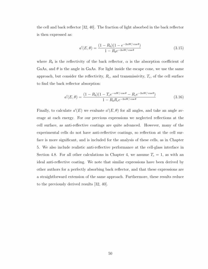
the cell and back reflector [32, 40]. The fraction of light absorbed in the back reflector
is then expressed as:
a′(E, θ) =(1−Rb)(1− e−2αW/ cos θ)
1−Rbe−2αW/ cos θ(3.15)
where Rb is the reflectivity of the back reflector, α is the absorption coefficient of
GaAs, and θ is the angle in GaAs. For light inside the escape cone, we use the same
approach, but consider the reflectivity, Rc, and transmissivity, Tc, of the cell surface
to find the back reflector absorption:
a′(E, θ) =(1−Rb)(1− Tce−αW/ cos θ −Rce
−2αW/ cos θ)
1−RbRce−2αW/ cos θ(3.16)
Finally, to calculate a′(E) we evaluate a′(E, θ) for all angles, and take an angle av-
erage at each energy. For our previous expressions we neglected reflections at the
cell surface, as anti-reflective coatings are quite advanced. However, many of the
experimental cells do not have anti-reflective coatings, so reflection at the cell sur-
face is more significant, and is included for the analysis of these cells, as in Chapter
5. We also include realistic anti-reflective performance at the cell-glass interface in
Section 4.8. For all other calculations in Chapter 4, we assume Tc = 1, as with an
ideal anti-reflective coating. We note that similar expressions have been derived by
other authors for a perfectly absorbing back reflector, and that these expressions are
a straightforward extension of the same approach. Furthermore, these results reduce
to the previously derived results [32, 40].
50

Chapter 4
Angle Restriction in GaAs Solar Cells
4.1 Motivation
In this chapter, we consider the effects of limiting the solar cell emission angle in GaAs
solar cells. By limiting the solar cell emission angle, as discussed in the previous chap-
ter, photons emitted by radiative recombination are less likely to escape from a solar
cell, reducing dark current and increasing efficiency. This photon recycling effect is
inherent in Shockley and Queisser’s original detailed balance analysis, but the limited
emission angle case was not considered explicitly [29]. While it has been calculated
that limiting emission angle could yield efficiencies exceeding 40%, more recent work
analyzing this effect in a planar GaAs cell concluded that no advantage would exist
for a realistic material owing to non-radiative recombination [32]. In contrast, we
find that utilizing a light-trapping-rather than planar-cell geometry mitigates losses
from non-radiative recombination, so significant benefits are possible with angle re-
striction. In fact, using the detailed balance model introduced in the last chapter, we
demonstrate that efficiencies exceeding 38% are potentially achievable with limited
emission angle and an ideal back reflector.
As discussed in the previous chapter, for cells with a light-trapping structure,
limiting the solar cell emission angle reduces the optical escape cone and enhances the
light trapping effect [7, 36]. Previously, efficiency benefits under angular restriction
have been considered with silicon in a light-trapping geometry [30]. However, photon
recycling benefits are minimal due to low radiative efficiency in silicon, and were not
included in the model. Here we consider a light trapping GaAs cell, where photon
recycling is much more prominent owing to high radiative efficiency in GaAs. Thus
51

while previous work has considered either light trapping or photon recycling, the
thin, light trapping GaAs solar cells considered here maximize both of these effects,
and we find a new regime of higher efficiencies that were not previously considered
achievable for a single junction solar cell under one sun illumination [30, 32, 47].
We also illustrate that a light trapping geometry allows for thinner cells with higher
efficiencies, significantly increasing the feasibility of the scheme.
While an angle restriction system, like a concentrator system, will require solar
tracking, the one-sun nature of the angle restricting system avoids the deleterious
heating and series resistance effects associated with high concentrations that were
mentioned in the previous chapter [33-35]. Furthermore, the light trapping nature of
the cells allows for cells that are 1/60th the thickness of current technology with full
light absorption. Assuming that junctions and window layers can be fabricated with
high quality in such a thin layer, this allows some of the materials savings associated
with concentrating systems to be realized in a flat plate geometry, without the high
aspect ratio optics found in traditional high concentration systems. We thus envision
a flat plate tracking system with thin, light trapping GaAs cells operating efficiencies
significantly higher than those achievable today.
4.2 Angle Restriction in a Light Trapping GaAs
Cell: Limits to Efficiency
4.2.1 Cell in the Radiative Limit
Using the expression for the absorptivity found in the previous chapter, along with
the air mass 1.5 direct solar spectrum (AM 1.5 D)1 and the optical constants of
GaAs, detailed balance efficiencies were calculated for various GaAs cell thicknesses,
1This is the standard solar spectrum for terrestrial applications. In these calculations we utilize
the direct, rather than global, solar spectrum, which includes only light coming directly from the
sun. Scattered, diffuse solar illumination from clouds or air particulates are included in the global
spectrum. However, limiting the emission angle will reduce the absorption of this diffuse light, and
therefore we consider only the direct portion of the solar spectrum.
52

assuming silicon nitride on both sides of the cell in the modal calculation. As shown
in Figure 4.1a, As the angle of emission narrows, both light trapping and photon
recycling are enhanced. With narrow angle restriction, to about 70, cell performance
is independent of cell thickness, as increased light trapping allows all the light to be
absorbed within even a 50 nm thick cell, or approximately 1/60th of the material in
a conventional non-angle restricted cell.
The angular accuracy of a tracker is usually expressed as a concentration, with
higher concentrations corresponding to improved angular accuracy. As the angular
accuracy of the tracker must be smaller than the emission angle, concentration factors
which correspond to a given emission angle are marked in Figure 4.1a to illustrate the
tracking accuracy required. As 1000x trackers are currently commercially available,
with higher accuracies demonstrated in research systems, we see that very high single
junction efficiencies are possible using existing two-axis solar tracking technology
[48, 49].
4.2.2 Effect of Auger Recombination
While the results in Figure 4.1a are encouraging, they assume all recombination is
radiative, which is unrealistic in a real material. Since GaAs can be fabricated with
very high purity and excellent surface passivation via III-V capping layers, for now
we consider only Auger recombination as it is the sole intrinsic, unavoidable source of
non-radiative recombination [41, 46, 50-52]. As in the previous chapter, we include
Auger recombination in the detailed balance equation as:
∫ ∞0
S(E)a(E)dE =
∫Ωc
∫ ∞0
a(E)2
h3c2
E2
e(E−qVoc)/kT − 1dE cos(θ)dΩ + CWn3
i e3qVoc/2kT
(4.1)
where C is the Auger coeffcient of 7x10⁻³⁰cm6s−1, and ni is the intrinsic carrier con-
centration in GaAs [40, 41, 47]. In contrast to the expression in the previous chapter,
this expression is applicable under high injection, where the carrier concentration is
dominated by light generation and is proportional to nieqV oc/2kT . Since we are inter-
ested in the efficiency limits with only intrinsic sources of recombination, we assume
53

!"
!#
$"
$#
%"
&'()*+,)-./01
!"
!#
$"
$#
%"
&'()*+,)-./01
#",7
2"",7
!#",7
#"",7$=7
2""": $"": #":%;<""": #:
!"
!#
$"
$#
%"
&'()*+,)-./01
!
"
#
2 2"
3,45+ 6' &7*88*6, /91
Figure 4.1. Detailed balance efficiencies as a function of emission
angle for various thickness light trapping GaAs solar cells with thick
silicon nitride cladding. In panel a, all recombination is assumed to
be radiative with an ideal back reflector. In panel b, Auger recombi-
nation is accounted for assuming an ideal back reflector. In panel c,
the back reflector is assumed to have 98% angle-averaged reflectiv-
ity, as is typical in silver, and Auger recombination is included. The
dotted lines indicate the concentration factors which have the same
degree of angular restriction to illustrate the tracking difficulty.
54

that the cell is very lightly doped, so it will operate in high injection. High qual-
ity material with a Shockley-Reade-Hall lifetime greater than 14.3 µsec and surface
recombination velocity less than 1.75 cm/sec for a 500 nm thick cell is required for
Auger recombination to be dominant at open circuit.
With increased voltage from photon recycling, Auger recombination increases rel-
ative to radiative emission. Thus, as Figure 4.1b illustrates, the effect of Auger
recombination is greatest for narrow emission angles, and there is little benefit for
emission angles below one degree. Interestingly, thinner cells show the best perfor-
mance for small emission angle because the Auger term is minimized while enhanced
light trapping allows for full absorption.
4.3 Ideal and Non-Ideal Back Reflectors for a Light
Trapping Cell
4.3.1 Effect of a Non-Ideal Back Reflector
While a nearly ideal back reflector may be achieved utilizing a dielectric stack reflec-
tor in air, a metallic back reflector is more likely to be cost effective [53]. However,
an imperfect back reflector will reduce the absorbed solar flux and photon recycling
via parasitic absorption of solar and radiatively emitted photons. Using expressions
found in Section 3.4.2 in the previous chapter, we calculate efficiencies for a 98%
reflective rear surface, as is typical for silver, in Figure 4.1c [54]. While the benefits of
limiting emission angle persist, particularly for thinner cells, the maximum achievable
efficiency is significantly reduced. In contrast to the ideal reflector case, the perfor-
mance of cells of all thicknesses converge for sufficiently limited angles. While these
results demonstrate the feasibility of the scheme, they also indicate the importance
of a highly reflective back surface, and suggest that either dielectric or metallodi-
electric back reflectors with higher reflectivity may be worth the additional cost and
fabrication difficulties.
55

4.3.2 Dielectric Mirrors Approaching Unity Reflectivity
Given the importance of an ideal back reflector for achieving maximum efficiencies
with angle restriction scheme, it is important to understand how closely an ideal om-
nidirectional back reflector could be approximated with a real optical structure. For
this purpose we examined a chirped, multilayer dielectric mirror, similar to the Bragg
stacks mentioned in Chapter 1, with an air gap separating the cell and the mirror.
Such dielectric omnidirectional reflectors with light incident from air have been fab-
ricated and experimentally validated in the visible regime, with the results closely
matching calculations [53]. However, we desire a mirror with high omnidirectional
reflectivity from about 400 to 870 nm, while the previous workers used ZnS, which
absorbs below 590nm. 2
We therefore have performed some simple calculations to show that our wavelength
requirements can be achieved with a similar approach. Rather than a ZnS/SiO2
stack, we consider a mirror made from alternating layers of TiO2 and SiO2, sacrificing
index contrast for transparency in the blue. Figure 4.2 shows the results of these
calculations [55]. We consider a dielectric stack with 200 TiO2/SiO2 layers, with an
initial thicknesses of 125 nm and 190 nm, respectively, and linear chirping to 30% of
the initial thickness values. For this structure, unity reflectivity is achieved or very
closely approached for all angles across the wavelength range of interest, giving an
angle and wavelength averaged reflectivity of 99.999%. We also consider a thinner
structure with sixty TiO2/SiO2 layers, with initial thicknesses of 136 nm and 203 nm,
respectively, and linear chirping to 30% of the initial thickness as before. Performance
is excellent except at oblique angles, and is omnidirectional at the radiative emission
wavelengths, giving an overall angle and wavelength averaged reflectivity of 99.6%.
Depending on the cell thickness, such a reflector may give similar performance with
less fabrication difficulty than the 200 layer stack. Thus, we find that a dielectric
2While there is solar radiation below 400 nm the external quantum efficiency in GaAs cells is low,
owing to absorption in the window layer [39]. In addition, GaAs has absorption lengths less than
15 nm in this portion of the spectrum. Thus, more than 96% of the ultraviolet light is absorbed on
the first pass in a 50 nm thick cell and avoids the back reflector.
56

!
!"#$%$&'() *&+,
-&'%$*.,
/00 100 200 300 400 500
0
60
/0
20
40
074
0741
075
0751
8
"
!"#$%$&'() *&+,
-&'%$*.,
/00 100 200 300 400 500
0
60
/0
20
40
071
072
073
074
075
8
Figure 4.2. Calculated reflectivity in air as a function of incidence
angle and wavelength from 400 to 870 nm. a) Reflector with 200
TiO2/SiO2 layers with initial thickness of 125 nm/190 nm and lin-
ear chirping to 30% of the initial thickness. b) Reflector with 60
TiO2/SiO2 layers with initial thickness of 136 nm/203 nm and lin-
ear chirping to 30% of the initial thickness.
57

stack with broadband omnidirectional calculated reflectivity closely approximating
unity is achievable, and have also demonstrated a design that sacrifices reflectivity at
oblique angles for simpler fabrication.
4.4 Comparison with a Planar Cell Geometry
Figure 4.3 gives analogous results for a planar, rather than light-trapping, cell geom-
etry using expressions derived in Section 3.4.4 of the previous chapter. As we expect,
thinner cells have low efficiencies in a planar geometry owing to poor absorption.
Thus, for the Auger-limited case, significantly higher efficiencies are achievable with
the light-trapping geometry. In fact, we would expect such a trend in any cell where
bulk recombination processes, like Auger or Shockley-Read-Hall recombination, are
dominant. However, with a metallic back reflector, the achievable efficiencies are
similar in the light-trapping and planar cases, though these efficiencies are achievable
in a much thinner cell with the light-trapping geometry. Thus, light trapping allows
for much thinner cells in all cases, and with an excellent back reflector it allows for
significantly higher overall efficiencies.
4.5 Comparison to Previous Work: The Radiative
Efficiency Approach
Previously, Martı and co-workers have argued that a limited emission angle scheme
would not be feasible in planar GaAs, as a ratio of non-radiative to radiative lifetime of
0.1 eliminated any benefit [32]. While a voltage dependent internal radiative efficiency
is inherent in the more realistic Auger recombination model presented previously, we
also consider a model which allows for explicit variation of the internal radiative
efficiency. This allows for comparison with the previous work. We find that with a
light-randomizing geometry even reasonable levels of non-radiative recombination are
not disastrous to the scheme.
To include non-radiative recombination, we re-write the detailed balance equation
58

Figure 4.3. Detailed balance efficiencies as a function of maximum
emission angle for various thickness planar GaAs solar cells. In panel
a, all recombination is assumed to be radiative with an ideal back
reflector. In panel b, Auger recombination is accounted for assum-
ing an ideal back reflector. In panel c, the back reflector is assumed
to have 98% angle-averaged reflectivity, as is typical in silver, and
Auger recombination is also included. The dotted lines indicate the
concentration factors which have the same degree of angular restric-
tion to illustrate the tracking difficulty.
59

as:
∫ ∞0
S(E)a(E)dE = 1 +R
[∫Ωc
∫ ∞0
a(E)2
h3c2
E2
e(E−qVoc)/kT − 1dE cos(θ)dΩ
](4.2)
where R times the radiative emission gives the non-radiative recombination [56]. Then
the external radiative efficiency, or the fraction of recombination events that result in
light escaping the cell, is:
ηext =1
1 +R(4.3)
Parallel to previous analysis of light emitting diodes, we have modified an expression
relating the external and internal radiative efficiency of a randomizing bulk slab with
an ideal back reflector to account for narrowing of the escape cone by a factor of
sin2(θ) [46].
ηext =ηint sin2(θ)/4n2
sin2(θ)/4n2 + (1− ηint)αW(4.4)
Considering the radiatively emitted light from a planar cell gives a parallel expression
for the external radiative efficiency in this geometry:
ηext =ηint(1− aint)1− ηintaint
(4.5)
where aint is the probability that an internally emitted photon will be re-absorbed
before it escapes the cell, which has been modified to account for a limited emission
angle [57].
aint = 1− (1− e−2αW ) sin2(θ)
4n2αW(4.6)
For non-unity internal radiative efficiency, external radiative efficiency is reduced
as the emission angle is limited, leading to relatively more non-radiative recombina-
tion. Also, thicker cells have lower external radiative efficiency for a given internal
radiative efficiency, as we expect. In the above expressions, the fraction of the light
within the escape cone under no angle restriction is approximated as 1/4n2, a ray
optics result. To account for modal structure in thin cells, we replace 1/4n2 with
half the fraction of total optical modal density from radiating, as opposed to trapped,
60

modes as defined by the Stuart and Hall absorptivity model presented in the previous
chapter [45]. This corresponds to the escape cone in the bulk ray optics limit with the
factor of one half due to escape occurring only from the top of the cell. For a closer
comparison to Martı’s model, the cladding layers considered in the main manuscript
are omitted in the modal calculation, and are replaced by air.
()
(*
(+
&"
&(
&)
,-./01#/23456
!"#$
%""#$
(!"#$!""#$
&'$
% %"
7#891 :- ,$0;;0:# 4<6
%!
("
(!
&"
,-./01#/23456
!"#$
%""#$
(!"#$
!""#$
&'$
!
"
Figure 4.4. Detailed balance efficiency calculations for a textured
(a) and planar (b) cell geometry with a constant internal radiative
efficiency of 90%. An ideal back reflector and an air front interface
are assumed. Note that for the textured case the 3 µm thick cell
performs worse than the 500 nm thick cell. This is due to reduced
external radiative efficiency in the 3 µm cell and nearly full light
absorption in the 500 nm cell.
Figure 4.4 shows efficiency results for 90% internal radiative efficiency in the planar
and light trapping cases. As noted, previous work considering non-randomizing cells
61

found that benefits did not persist for non-unity internal radiative efficiency, and our
results are consistent with this conclusion, despite slight differences in the models [32].
However, for a given internal radiative efficiency and thickness a light trapping cell
will have a larger external radiative efficiency and less non-radiative recombination
than a non-randomizing cell. Thus, as in the main manuscript, there are significant
efficiency benefits to angle restriction in these cells, particularly if the cells are thin.
Clearly, then, a light trapping structure is key to overcoming non-radiative losses and
obtaining the maximum benefit in an angle restriction strategy.
4.6 Radiative Efficiency in Current GaAs Cell Tech-
nology
While this chapter has suggested the significant advantages possible with angle re-
striction, it is unclear if current GaAs technology has sufficiently low non-radiative
recombination to benefit. Recently, there has been considerable progress in increasing
the world record single junction efficiencies via GaAs solar cells with high voltages,
suggesting a high material quality and a good back reflector [39, 58]. While these cells
are likely thick with a planar geometry and are thus unlikely to benefit significantly
from angle restriction, they are an excellent example of current GaAs material qual-
ity, and external radiative efficiencys have been calculated [37]. Thus, by assuming
a 2µm thick planar cell with 98% back reflectivity, we can estimate the internal ra-
diative efficiency, and determine the feasibility of the angle restriction approach with
current material quality. Using the same procedure as was used above to find ηext for
a planar cell with an ideal reflector, we find
ηext =ηint (1− atot)1− ηintacell
(4.7)
62

where atot is the total reabsorption of light in the cell and loss back reflector and acell
is the reabsorption of light in the cell. Then,
atot =
(1− 1
2n2
)+
1
2n2atot,esc (4.8)
and
acell = atot =
(1− 1
2n2
)(1− arefl,trap) +
1
2n2acell,esc (4.9)
where esc denotes light within the escape cone, trap denotes light outside the escape
cone, and arefl denotes light absorbed in the lossy reflector. Finally, then:
atot,esc =
(1− 1− e−αL
αL
)+
1
2R
(1− e−αL
αL
)(1− e−αL
)+
1
2(1−R)
(1− e−αL
αL
)(4.10)
acell,esc =
(1− 1− e−αL
αL
)+
1
2R
(1− e−αL
αL
)(1− e−αL
)(4.11)
arefl,trap =(1−R)
2
(1− e−αL)
αL
(1 + e−αL)
(1−Re−2αL)(4.12)
where R is the reflectivity, L = W/ cos(θ), and we average over all angles within and
outside the escape cone. For an external radiative efficiency of 22.5%, as calculated by
Green, we find an internal radiative efficiency of 92.6%, very similar to the 90% IFY
assumed in figure 2 [37]. Thus, a thin, light trapping cell with material quality similar
to current GaAs technology should show significant benefit with an angle restriction
scheme, illustrating its immediate feasibility.
4.7 Broadband Angle Restrictor Designs
Throughout the previous analysis, we have assumed a device which facilitates light
in-coupling within the specified angle without loss, while excluding all other light
spanning wavelengths from the blue edge of the solar spectrum to the band edge
of GaAs at 870 nm. While there has been some discussion in the literature about
63

possible strategies for designing such an angle restricting coupler, we are not aware
of designs whose performance has been optically analyzed [30, 59]. Other than the
design of an emission angle limiting coupler, our scheme relies largely on existing
technologies, such as tracking and high quality GaAs cells. Thus, to complete the
feasibility argument, two broadband angle restrictor designs are presented and their
performance analyzed, with experimental work showing the early fabrication of one
design.
Figure 4.5a,b illustrates a coupler that utilizes total internal reflection within
dielectric cone-type structures based on a modified compound parabolic concentrator
(CPC) shape [60]. The cone-like structures have the side curvature of a CPC, but
the curvature of each portion of the side, as defined by the CPC acceptance angle, is
adjusted so that the top of the cone-type object has a hexagonal cross-section, allowing
for close-packing. The small bottom openings are circular, even though the tops are
hexagonal. A double close-packed array of cones, separated by a perfect, broadband
reflector with small holes at the cone bottoms, completes the coupler design. The
broadband reflector is important for reflecting light entering at large angles back into
the solar cell. Unlike a single array of these cone type structures, the double array
gives uniform, near normal illumination of the cell, minimizing reflection losses and
avoiding the deleterious effects of non-uniform illumination on solar cell performance.
Because this coupler functions on ray optics principles, it is naturally broadband.
A thinner coupler allows for easier integration with existing systems and lower
materials cost. Since this coupler is based on ray optics, it can be built on any scale
much larger than the wavelength. To minimize the coupler height, we set the scale
so that the reflector openings are in the ray optic limit (4µm diameter). As the
maximum CPC acceptance angle decreases, narrowing the allowed emission angles,
the optimal height of the cone structure increases [60]. Thus, to more strictly limit
the emission angle, we must either tolerate a thicker coupler structure or truncate
from the optimal CPC height.
In Figure 4.5c, we compare three designs limited to 1mm in height by using ray
tracing to determine the reflectivity. For the design marked 3.7, with the least
64

Figure 4.5. a,b) Dielectric coupler schematic. c) Calculated dielec-
tric structure reflectivity for 300 nm (dashed) and 870 nm (solid)
light. Labels indicate maximum emission angle that defines the
sides. Observed angles are larger due to refraction in the dielec-
tric. d,h) Detailed balance I-V curves for light trapping cells with
Auger recombination and an ideal back reflector with and without
(90o) angle restrictors. Legends give efficiency, cell thickness, and
design angle. e,f) Schematic of metal array coupler and SEM of
fabricated structure. g) Calculated reflectivity for a 98% reflective
metal surface.65

angular restriction, there is no truncation, while for design with maximal restriction,
marked 2, the shape is truncated to approximately 30% of its optimal height. Because
of the large size of the coupler relative to the wavelengths of interest, we analyze the
coupler performance using ray tracing, with silicon nitride dielectric structures. The
ray tracing was performed using a home-built Matlab code that traces rays at each
in-plane and out-of-plane angle, and averages rays starting at different points on
the cone top and over the in-plane angles, to find the results in Figure 4.5c. The ray
traces also assume ideal anti-reflection coatings and the angle restrictor-cell and angle-
restrictor air interfaces. We see excellent angular cutoff, and a broadband response,
as illustrated by the curves for 300 and 870 nm. For the more truncated designs, the
angular cut-off is less abrupt, but begins at smaller angles.
The ray tracing results can then be incorporated into the detailed balance cal-
culation by replacing the factors of sin2(θ) in the previous calculations with angular
transmission averages. Figure 4.5d shows current-voltage curves for the three different
coupler designs on a 250 nm thick cell with Auger recombination and an ideal back
reflector, as well as results for cells with no angularly restricting coupler. We see that
the most severely truncated design performs the best, with a four absolute percent
efficiency increase over a thicker cell with no coupler, and a seven absolute percent
increase over a no-coupler cell of the same thickness. While there is an approximately
100 mV increase in open circuit voltage, the short circuit current only increases by
about 3 mA/cm2, so there should be no significant heating or series resistance effects,
as in concentrator systems. Thus, this coupler design could be used to experimentally
demonstrate significantly improved performance due to limited emission angle.
In Figure 4.5e-h, we analyze a similar coupler that is easier to fabricate, and show
an initial fabrication of the structure over a small area using two-photon lithography.
This coupler has a single, rather than double, array and uses metal coated cups,
rather than total internal reflection in a dielectric. To limit degradation in device
performance, the illuminating holes at the bottoms of the cups should be within the
carrier diffusion length, so the coupler must be relatively small (micron) scale while
remaining ray optical. With 98% metal reflectivity and neglecting the gaps between
66

cups, ray tracing results coupled to the detailed balance model suggest a significant
performance increase.
The fabricated structures shown in Figure 4.5 were written into IP-L resist using
the Nanoscribe Photonic Professional two-photon lithography system. To prepare
the sample for writing, optical coupling fluid was placed on one side of a glass slide,
and IP-L placed on the other. After writing, development in 2-propanol for 20 min
utes, which removes all unwritten IP-L and the optical coupling fluid, was followed by
drying of the glass slide. The structures written in resist remained on the glass slide,
and were then coated with about 20 nm of sputtered chromium to aid conductivity
for imaging. While these devices show the feasibility of creating such a structure,
two-photon lithography is not suitable for large area fabrication, and some sort of
stamping procedure would be desirable. In addition, further work would be required
to deposit high reflectivity metallic coatings in such high aspect ratio structures [61].
4.8 Narrowband Angle Restrictor Design
While it is clear that light trapping GaAs cells are preferable for angle restriction,
world-record quality cells made currently are planar [39, 43]. This is due to the
difficulty of texturing an epitaxially grown film while maintaining high material and
surface quality. In fact, to make a light trapping GaAs cell adding a transparent high
index light randomizing surface, such as a textured layer of titanium dioxide, silicon
nitride, or gallium phosphide,3 seems the most likely approach. In a planar cell, only
photon recycling may be enhanced with angle restriction, as there is no mechanism
to randomize incoming light, limiting the cell to dual pass absorption. Since the
emitted light of interest for photon recycling occurs over a narrow wavelength range
corresponding to the cell photoluminescence (approximately 800-870 nm in GaAs),
3While gallium phosphide is not transparent over the entire range of interest, light above the
gallium phosphide bandgap may be largely absorbed on the first pass through the cell, depending on
the cell thickness. Thus, gallium phosphide, with its higher refractive index, may be an attractive
option for backside scattering.
67

only a narrowband angle restricting structure is required. Furthermore, a narrowband
structure allows much of the diffuse solar
As shown in Figure 4.6b, the narrowband angle restrictor design consists of alter-
nating high and low index with large refractive index contrast to increase the angular
range of reflection [7, 62, 63]. While the design is not strictly periodic, the angular
properties can be understood from the Bragg condition
cos θ =mλ
2Γ(4.13)
where θ is the angle of maximum reflectivity, λ is the wavelength, Γ is the period
of the multilayer, and m is an integer [64]. For shorter wavelengths maximum re-
flectivity occurs away from normal incidence, providing angle restriction for emitted
light and excellent transmission at normal incidence in both the designed and fabri-
cated structures. In a standard Bragg stack with discrete high and low index layers,
the Bragg condition is applicable and angle restriction occurs. However, such simple
structures also suffer from undesirable reflections at normal incidence owing to second
order (m = 2) reflecting bands, as well as ripple-type reflections (see Figure 5.2 in
the next chapter). Modifying these structures to include gradual index variation, as
shown in Figure 4.6, known as a rugate or graded index structure, eliminates these
undesirable reflections, allowing Jsc to be maintained with angle restriction.
Figure 4.6 illustrates a rugate design for angle restriction in GaAs, based on ref-
erence [65], which eliminates both the second-order reflecting band and the smaller
ripple-type reflections near normal incidence [66-68]. Unlike the simple Bragg stacks
discussed in the next chapter, this angle restrictor is designed to perform under glass,
as in an installed solar array. Our concept is that the angle restrictor would be de-
posited directly on the cell, with the glass covering attached with an index matched
polymer to avoid any air gaps between the glass and angle restrictor. For a comparison
case without angle restriction we consider a quintic-type graded index anti-reflection
(AR) coating with the same index range and thickness as our angle restrictor de-
posited at the same glass/cell interface [69]. Thus, the performance of the graded
68

Figure 4.6. a) Refractive index profile of the graded-index AR coat-
ing used as a comparison case. Index range and optical thickness
are matched to rugate angle restrictor. 0 represents the interface
with the covering glass. b) Refractive index profile of rugate angle
restrictor. 0 represents the interface with the covering glass.
69

index angle restrictor is compared to a graded index AR coating, assuming both are
under glass.
For this point design we assume the minimum refractive index in the rugate angle
restrictor and graded index AR control is 1.5 and assume a TiO2/SiO2 co-deposition
process with a maximum index of 2.5 [70-72]. (We note that if high index TiO2 cannot
be achieved with co-deposition, similar increases in performance can be achieved with
lower index TiO2 films, though the currents and overall efficiencies are somewhat
reduced for both the graded index AR control and the rugate angle restrictor due to
increased reflection.) Figure 4.7 gives the calculated reflectivity for both the graded
index AR control and the rugate angle restrictor design [43, 55]. The rugate angle
restrictor design has normal incidence transmission very similar to the graded index
AR control and nearly complete suppression of the second-order reflecting ban [65, 69].
Angle restriction to about 20o is achieved near the peak in the emission spectrum,
and, away from the angle restricting region, transmission is very similar for both
the graded index AR control and the rugate angle restrictor across all angles. Thus,
for most of the spectrum, diffuse light should be utilized equally well for the angle
restrictor and graded index AR coating.
To quantify this further, in Figure 4.8 we estimate the short-circuit current in
the cell as a function of the light incidence angle based on the cell internal quantum
efficiency (IQE) spectrum and the transmission spectrum, including reflections from
the top surface of the glass. The predicted current with the rugate angle restrictor is
99.98% of the graded-index AR comparison value at normal incidence, and remains
above 99% up to 25 degrees. Furthermore, the minimum current with the rugate
angle restrictor at any angle is 77% of the graded index AR control value, so we
expect a very large portion of the diffuse light to be captured with this design.
Next, we evaluate the efficiencies of cells with the graded index AR control and
rugate angle restrictor using the modified detailed balance model with short-circuit
current values from Figure 4.8. We use a multipass model to account for reflections
between the cell/glass interface, where the rugate angle restrictor or graded index
AR is deposited, and the glass/air interface. Unlike previous cell models considered
70

Figure 4.7. a) Calculated reflectivity values for the graded index
AR coating comparison structure. Structure is assumed to be under
glass and immediately above a GaAs cell with 20 nm AlInP window
layer. b) Calculated reflectivity values for the rugate angle restrictor
design. Structure is assumed to be under glass and immediately
above a GaAs cell with 20 nm AlInP window layer. All calculations
use the transfer matrix method with the rugate profile divided into
1 nm thick layers.
71

0 20 40 60 800
0.2
0.4
0.6
0.8
1
Angle (o)
No
rma
lize
d S
ho
rt!
Circu
it C
urr
en
t
Graded Index AR Control
Rugate Angle Restrictor
Restrictor/Control Current Ratio
Figure 4.8. Predicted Jsc as a function of light incidence angle for the
rugate angle restrictor (red line) and graded index AR control (blue
line) structures under glass. Values are normalized to the graded
index AR structure at normal incidence. The ratio of the Jsc values
is also plotted (dotted purple line).
in this chapter, to facilitate comparison with experimental cells, a surface recombi-
nation velocity is included, as in Equation 3.4. As in Figure 4.9, we vary the surface
recombination velocity S, assuming an ideal back reflector, thereby varying the ERE
up to the Auger limit . However, as the Auger limit is dependent on cell thickness
and doping, we also perform the calculation at 100% ERE. As we expect, for higher
ERE cells there is a larger improvement in efficiency with angle restriction. As shown
in 4.9, for this point design we expect a 1% relative efficiency increase for cells with
ERE values corresponding to the current GaAs world record [38], and a 2.5% relative
efficiency increase for Auger limited cells with a 27mV Voc enhancement.
Because of this design’s wide acceptance angle, it can also be used under a con-
ventional concentrator, rather than to collect diffuse light. Because currents are
maintained out to 25o, we assume a conventional concentrator with an input angle
of 2 degrees, and an output angle of 25 degrees, operating at the thermodynamic
concentration limit of 146.6 suns [60] . We further assume that light output from
72

0 20 40 60 80 10025
26
27
28
29
30
Cell External Radiative Efficiency (%)
Ce
ll E
ffic
ien
cy (
%)
Graded Index AR Control
Rugate Angle Restrictor
Current World Record
Auger Limit
Figure 4.9. Predicted efficiency as a function of external radiative ef-
ficiency for the rugate angle restrictor (red) and the graded-index AR
control (blue). The solid line indicates the range ERE values attain-
able with current GaAs cells. The end of the solid line corresponds
approximately to ERE values for current world record cells [38]. The
dotted line indicates ERE values beyond current world record cells
and terminates at the Auger limit (grey line). Finally, the dots in-
dicate efficiency values at the radiative limit (ERE=100%). Note
that in the ERE range considered experimentally (3-16%) the angle
restrictor and control lines are nearly overlaid, indicating a small
voltage enhancement with angle restriction in this region, similar to
the voltage enhancement we observed experimentally.
73

0 20 40 60 80 100
29
30
31
32
33
Cell External Radiative Efficiency (%)
Ce
ll E
ffic
ien
cy (
%)
Graded Index AR Control
Rugate Angle Restrictor
Auger Limit
Current World Record
Figure 4.10. Predicted efficiency as a function of external radiative
efficiency for the rugate angle restrictor (red) and the graded index
AR control (blue) under a 146.6x concentrator with 25 degree output
angle. The solid line indicates the range ERE values attainable with
current GaAs cells. The end of the solid line corresponds approxi-
mately to ERE values for current world record cells at one sun [38].
The dotted line indicates ERE values beyond current world record
cells and terminates at the Auger limit (grey line). Finally, the dots
indicate efficiency values at the radiative limit (ERE=100%).
74

the concentrator is evenly distributed over the angular range from 0 to 25o, and de-
termine the predicted current and efficiency for the cell. As in figure 4, at low ERE
values current losses from the wide range of input angles outweigh voltage gains, and
efficiencies are slightly reduced with angle restriction. However, with a high ERE cell,
efficiency gains with angle restriction are possible under fairly high concentrations.
4.9 Conclusions
Developing a detailed balance model for a thin, light trapping GaAs solar cell with
limited emission angle, we have found efficiencies above 38% may be achievable with
a single junction solar cell. We identify a regime of efficiencies significantly higher
than those previously predicted for realistic cells with limited emission angle, by max-
imizing both light trapping and photon recycling effects. A light trapping geometry,
high quality material, an excellent back reflector, and a very thin cell are critical to
reaching the highest single junction efficiencies. A metallic back reflector allows for
the use of very thin cells while maintaining, and slightly improving, efficiency rela-
tive to a thick non-angle restricted cell. However, much larger efficiency benefits are
possible with an ideal back reflector, which can be closely approximated by a dielec-
tric mirror. These results suggest that limiting emission angle with a light trapping
GaAs cell and an excellent back reflector could provide a new route to achieving high
efficiencies without a tandem or third generation cell.
Encouragingly, this scheme relies largely on existing technology, with the excep-
tion of a low-loss, broadband, angularly restricting coupler. We therefore analyzed
two broadband angle restrictor designs, found that these couplers could produce sig-
nificant performance increases, and demonstrated initial fabrication of one design.
Finally, while broadband couplers may be preferable for light trapping cells, there is
little benefit for planar cells where photon recycling is the only benefit. For current
planar cells, we presented a rugate structure point design, and illustrated that a 1%
efficiency benefit could be realized with existing cells. Thus, we have identified a new
regime of very high single-junction efficiencies achievable by limiting emission angle,
75

laid out the critical factors necessary to realizing these efficiencies, and considered
both broadband and narrowband angle restrictor designs.
76

Chapter 5
Experimental Demonstration of Enhanced
Photon Recycling in GaAs Solar Cells
5.1 Motivation
For ideal solar cells where all recombination is radiative, photons emitted from the
cell are the sole source of carrier loss, as in the detailed balance limit introduced
in Chapter 3 [29]. Cells approaching this radiative limit have significantly higher
efficiencies, as evidenced by recent world record GaAs cells, and can also exhibit new
effects owing to the significant number of radiatively emitted photons [39, 43, 73].
As we have shown previously, optically limiting the angles of emitted light causes
emitted photons to be recycled back to the cell, leading to enhancement in voltage
and efficiency. Despite this theoretical prediction, until recently even the highest
efficiency solar cells were not close enough to the radiative limit for such an effect to
be observed [32, 74].
However, with the introduction of cells lifted off the growth substrate, GaAs cells
have shown significnant gains in efficiency due to Voc increases, indicating an increase
in the external radiative efficiency (ERE) of the cell [39, 43, 73]. In these lifted-off
GaAs cells radiatively emitted photons are reflected from a metallized back surface
instead of being absorbed in the substrate, resulting in a large increase in ERE and Voc
[40, 73]. As radiative recombination is dominant in high quality GaAs, these lifted-
off cells perform near the radiative limit and are therefore suitable for experimentally
demonstrating enhanced photon recycling and Voc via angle restriction of emitted
light. In fact, it was recently demonstrated that a voltage increase could be observed
77

in such cells by placing a reflecting dome above the cell to recycle emitted photons
[75].
Here, as proof of concept, we demonstrate enhanced photon recycling and Voc
experimentally using an optical element with angle restriction only over the narrow
wavelength range of emitted light in GaAs that is placed on a high quality GaAs
cell. We have designed a dielectric multilayer angle restrictor with excellent normal
incidence transmission and high reflectivity at oblique angles for radiatively emitted
wavelengths. Using this narrowband angle restrictor with a high quality GaAs cell, we
observe enhanced photon recycling and a resulting voltage increase. In other words,
simply placing an angle restrictor on the cell causes a voltage increase of 3.6 mV
without a change in current. In addition, we observe a 12% decrease in the radiative
component of the dark current, which is consistent with the observed Voc increase.
Considering a variety of cells, the largest Voc enhancements occur in cells that are
closest to the radiative limit, with maximum ERE values of 15.7%. Finally, we see
that more closely coupling the angle restrictor to the cell leads to greater Voc gains,
emphasizing the optical nature of the enhancement.
As was shown in Chapter 3, assuming the Voc does not closely approach the
bandgap, we may approximate the Voc under illumination in the radiative limit as:
Voc ≈ kT ln
( ∫∞EgS(E)a(E)dE∫
Ωc
∫∞Ega(E) 2
h3c2E2
e(E−qVoc)/kT−1dE cos(θ)dΩ
)= kT ln(Jsc/J0) (5.1)
where Jsc is the short-circuit current and J0 is the dark current, which is solely due
to radiatively emitted light. Restricting the emission angle causes photons generated
by radiative recombination to be recycled and reabsorbed within the cell rather than
emitted. Thus, enhanced photon recycling via angle restriction reduces J0 and in-
creases Voc. For realistic cells, emitted light forms a larger fraction of J0 in cells closer
to the radiative limit. Thus, high ERE cells, like the GaAs cells in these experiments,
are required for J0 to be reduced sufficiently with angle restriction that a voltage
increase may be observed. Furthermore, higher ERE cells should show larger volt-
age increases. For this reason, though the voltage increases in this proof-of-concept
78

experiment are modest, further improvements in GaAs cell technology, including the
introduction of light trapping cells as discussed in Chapter 4, could significantly in-
crease the performance benefits from angle restriction.
For terrestrial applications, we envision a flat plate, one sun, angle restricting
system with high quality GaAs cells. While tracking may be beneficial, high ac-
curacy tracking is not required as dielectric angle restrictors have a relatively large
acceptance angle. Furthermore, for cells in the ERE range considered here, narrow
angle restriction has limited benefit, as non-radiative recombination limits the possi-
ble voltage increase. Additionally, recent work has demonstrated the fabrication of
high ERE cells in other III-V materials, notably GaInP, suggesting that this approach
will become more broadly applicable with continued cell development, and could eas-
ily be incorporated with multijunctions [76]. Use with these cell technologies also
suggests early applications in military and space solar, where efficiency and weight
are paramount.
5.2 Narrowband Multilayer Angle Restrictor
While the previous chapter focused on broadband ray optical angle restrictors with
light trapping cells, the cells in this experiment are planar with high reflectivity spec-
ular back reflectors that are metallic, with reflectivity of 75.5%, or metallodielectric,
with reflectivity of 99.7%. The calculated reflectivity values refer to band edge (873
nm) emission angle-averaged within the GaAs. As the solar cells are planar and
do not incorporate light trapping, only the photon recycling enhancement will be
observed, as shown in Figure 5.1, and absorption will be dual pass. As enhanced pho-
ton recycling is the only angle restriction effect, we utilize a dielectric multilayer that
provides angle restriction only over the narrow range of wavelengths at the semicon-
ductor band edge where the GaAs cells emit light (see Figure 5.2). This narrowband
angle restriction allows diffuse, non-normal incidence light to enter over most of the
spectral range, as with the rugate structures shown in Section 4.8. Capturing this
diffuse light gives significant current ehancements relative to a broadband concentra-
79

Photon Recycling via Angle Restriction
•!Dual pass absorption with or without angle restriction, no
absorption enhancement
•!Current is reduced due to losses in the angle restricting optics
!
!
!
Absorbed Light (Jsc) Photon Recycling (Voc)
•!Calculations suggest ~10mV max Voc increase with ideal angle restriction
•!Since light is only emitted over a
narrow range of wavelengths, only narrowband angle restriction required
"#$%&!'(!)*+,-.!/!0,12,-3!43*56!
GaAs Solar Cell
Emitted Light
Incoming Light
Figure 5.1. With a planar cell, absorption of incoming light is dual
pass, regardless of angle restriction. In fact, slight reductions in
current are observed owing to losses in the angle restrictor. However,
enhanced photon recycling of emitted light and resulting voltage
increase will still occur, as emitted light is randomized. As light
is emitted only over a narrow wavelength range, only narrowband
angle restriction is required.
tor or angle restrictor. In addition, potential losses due to tracking errors are greatly
reduced, and simpler, cheaper trackers may be utilized. As was shown in Section 4.8,
we envision depositing such an angle restrictor in place of a traditional AR coat, so
the cost derives only from the added layers relative to a traditional AR coat.
As shown in Figure 5.2b, the angle restrictor design consists of alternating high
and low index layers with large refractive index contrast to increase the angular range
of reflection [7, 62, 63]. While the design is not strictly periodic, just as in Section 4.8,
the performance can be understood with reference to the Bragg condition (Equation
4.13). As shown in Figure 5.2, for shorter wavelengths maximum reflectivity occurs
away from normal incidence, providing angle restriction for emitted light and excellent
transmission at normal incidence in both the designed and fabricated structures. We
note that total internal reflection owing to the high index of GaAs already provides
significant photon recycling within the cell, and despite this, there is still a substantial
loss due to emitted light, as ERE estimates indicate [73]. As the measured reflectivity
in air (Figure 5.2d) demonstrates, the dielectric structure provides photon recycling
80
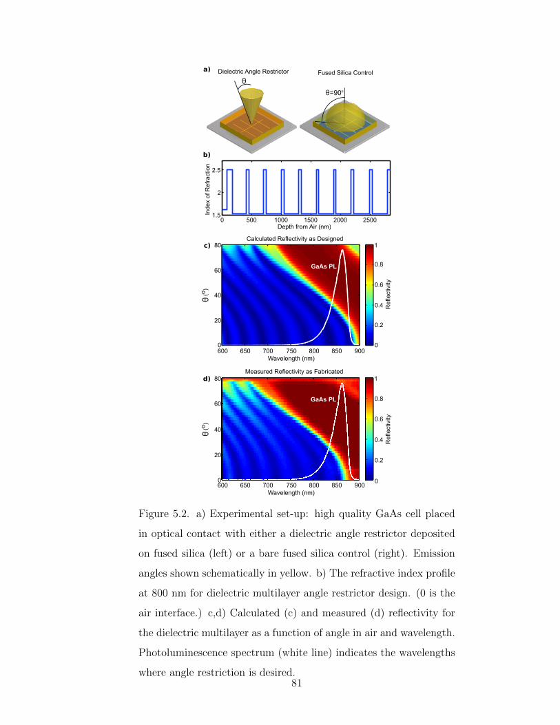
!"
#"
$"
%"
!"#$"%&'('&)
!"#$"%&'('&)
* 1** 0*** 01** +*** +1**0/1
+
+/1
C"J&89#E=;9H'E9:6;<
K6A"L9=#9!"#E5%&'=69
*
+*
,*
-*
.*
*
*/+
*/,
*/-
*/.
0
-** -1* 2** 21* .** .1* 3**
45("$"67&89:6;<
99:=<
*
+*
,*
-*
.*
*
*/+
*/,
*/-
*/.
0
-** -1* 2** 21* .** .1* 3**
45("$"67&89:6;<
!
!
!>3*=
!"#$%&'
!"#$%&'
?5$%@$5&"A9!"#$"%&'('&)95B9C"B'76"A
99:=<
!
D"5B@E"A9!"#$"%&'('&)95B9F5GE'%5&"A
C'"$"%&E'%9H67$"9!"B&E'%&=E F@B"A9I'$'%59?=6&E=$
&'()*+,-
Figure 5.2. a) Experimental set-up: high quality GaAs cell placed
in optical contact with either a dielectric angle restrictor deposited
on fused silica (left) or a bare fused silica control (right). Emission
angles shown schematically in yellow. b) The refractive index profile
at 800 nm for dielectric multilayer angle restrictor design. (0 is the
air interface.) c,d) Calculated (c) and measured (d) reflectivity for
the dielectric multilayer as a function of angle in air and wavelength.
Photoluminescence spectrum (white line) indicates the wavelengths
where angle restriction is desired.81

of light that would otherwise be emitted. This enhanced photon recycling occurs in
addition to the photon recycling via total internal reflection, which is unaffected by
the dielectric structure.
5.3 Dark Current Measurements
Theory clearly indicates that enhanced photon recycling via angle restriction will
result in a reduction of the radiative dark current. We therefore measured the dark
current characteristics of a single cell under both the angle restrictor and a bare fused
silica control optic, as in Figure 5.2a. Fused silica index matching fluid was applied at
the interface of the cell and the fused silica substrate to avoid extraneous reflections,
and the edges of both optics were coated with a gold reflector to avoid light escape
from the sides. (See Section 5.8 for further details.) In the high voltage region near
Voc, where radiative emission contributes most significantly to the dark current, we
see a clear decrease in dark current with angle restriction, as in figure 2a.
To quantify this we fit the dark current, J0, over the high voltage 0.6 to 1.1 V
region, to the double diode equation
J0 = J01(eq[V−JdarkRs]
kT − 1) + J02(eq[V−JdarkRs]
nkT − 1) (5.2)
where J01 is the high voltage dark current component, J02 is the low voltage com-
ponent, Rs is the series resistance, and n is the diode ideality factor [77, 78]. For
both the control and angle restriction curves, the fit is excellent over several orders
of magnitude. The fit deviates somewhat at very low currents, which we attribute
to shunt resistance and has been previously observed in similar cells [39]. As figure
2b shows, J02, Rs, and n are unchanged with angle restriction and n is very close
to two, indicating that the double diode model is valid [77, 78]. In contrast, the J01
term, which has the same voltage dependence as radiative recombination, shows a
12% decrease with angle restriction, well beyond the error of the fit. Thus, by simply
changing the optic above the cell to an angle restrictor, we observe a definite reduc-
82

-
.
/
0
1
2-
2.
+,));BC&*&D;);*9&%@;
E-2<2-F.2AGHD.= <2-F2.AGHD.= <IGHD.=
E-. !" #
!"
-34 -31 -35 2 2322-60
2-67
2-6/
2-68
2-6.
9(%)&:; <9=
>&*?'@**;#)<A=
23-4 23-47 23-1-3--1
-3--5
-3-2
$%&"" '(#)*(%
$%&"" '(#)*(%
$%&"" '(#)*(% +,)
A#:%; !;")*,H)(*
A#:%; !;")*,H)(*
A#:%; !;")*,H)(* +,)
#"
$%&'()*+
Figure 5.3. a) Representative dark current curves and double diode
fits for both the angle restrictor and control cases . Inset: a clear
reduction in dark current is evident near Voc for the angle restrictor
case. b) Double diode fitted parameter results with each bar rep-
resenting one of three trials on the same 15.7% ERE cell for both
the angle restrictor and fused silica control. The error bars repre-
sent 95% confidence intervals derived from the fit. Consistent with
reduced radiative loss, J01 shows a marked decrease with angle re-
striction while all other parameters remain unchanged.
83

tion in the dark current. Specifically, the reduction occurs in the high voltage dark
current component attributable to radiative loss, indicating that angle restriction is
enhancing photon recycling within the cell.
5.4 Voltage Enhancements Under Illumination
In addition to a reduction in dark current, we also expect a direct Voc enhancement
under illumination. Furthermore, this voltage enhancement should be larger for cells
with higher ERE, as more photons are available to be recycled via angle restriction.
We therefore measured light current-voltage curves for a set of four cells with differing
back reflector and material quality leading to significant variations in ERE across the
cells, as determined from the Jsc and Voc characteristics under the control optic. (See
SI for further model details.) Owing to a reflecting band in the optical coupler around
550 nm, we limited the spectrum in this proof-of-concept experiment to wavelengths
longer than 605 nm. (As in Section 4.8, this reflecting band can be eliminated with a
rugate filter optical design, but for the initial coupler we did not pursue these struc-
tures as they are more difficult to fabricate [65, 66].) As shown in Figure 5.4, when
we directly compare the control and angle restrictor on the same cell, current losses
of 3.5% to 5.3% are observed with angle restriction, consistent with the measured
normal incidence reflectivity of the angle restrictor. Without a change in the dark
current, a reduction in Jsc would normally produce a corresponding reduction in Voc,
as in equation (1). However, Voc increases of up to 2.5 mV are observed under angle
restriction for the highest ERE cells, as dark current reduction is the dominant effect.
Thus, angle restriction increases cell voltage without any change in the illumination,
despite a reduction in Jsc. Furthermore, as we expect for photon recycling, the voltage
change tracks the cell ERE.
Fortunately, these current losses are not intrinsic, and result from the simplicity of
our initial angle restrictor design, as illustrated in Section 4.8 [65, 66]. To isolate the
photon recycling effect, we adjust the solar simulator to equalize the currents between
the control and angle restrictor, as in figure 3b. Once Jsc values are matched for the
84

5 10 15−0.8
−0.6
−0.4
! J
sc (m
A)
5 10 15
−1
0
1
2
3
Cell External Radiative Efficiency (%)
Cha
nge
in V
oc (m
V)
Figure 5.4. Measured changes in open-circuit voltage (dark blue
line) and short-circuit current (green line) with angle restriction.
The set of four cells is plotted as a function of external radiative
efficiency (ERE) determined from Jsc and Voc under the control optic.
Variations in ERE occur between cells owing to differences in back
reflectors and material quality. The error bars are calculated from
standard deviation of five measured trials. The dotted white line
indicates the expected voltage increase based on a modified detailed
balance calculation. The light blue area shows the expected range
of the model based on uncertainty in Jsc, Voc, and temperature. As
the solar simulator flux is held constant, there are current reductions
(top) owing to normal incidence reflections in the multilayer angle
restrictor, and thus Voc increases are only seen in high ERE cells,
where the reduction in J0 outweighs the loss in Jsc, as in Equation
5.1.
85

angle restrictor and control, voltage increases ranging from 1.2 mV to 3.6 mV are seen
for all cells, with higher ERE cells showing larger voltage increases. As the 15.7%
ERE cell was also used for dark current measurements, we can compare the change
in J01 to the observed change in Voc. Since Voc = kT ln(Jsc/J0) and the J01 term is
dominant near Voc, the change in Voc should be approximately kT ln(J01/J′01), where
J ′01 indicates the average fitted value with the angle restrictor. Using this approach,
we predict from the dark current fits that the Voc increase should be 3.0 mV, which
is reasonably consistent with the measured value of 3.6 mV for this cell. Thus, we
observe a clear Voc increase with angle restriction that is consistent with our dark
current measurements, and an ERE trend that indicates enhanced photon recycling
as the mechanism.
5.5 Modified Detailed Balance Model
We also develop a model that directly relates the voltage increase to the optical char-
acteristics of the angle restrictor. While detailed balance is traditionally considered
an idealized model, as shown in Chapter 3, we have developed a more realistic detailed
balance model that includes the cell thickness, anti-reflective coating, back reflectors,
and Auger and surface recombination. Including these non-radiative processes allows
our model to be much more realistic than a traditional idealized detailed balance,
where non-radiative losses are neglected. In addition, we simply input the measured
short-circuit current, to avoid issues with the variability of the solar simulator lamp
spectrum. Thus, the current at a given voltage, J(V ) , in the modified model for
these cells is expressed as:
J(V ) = Jsc−∫ ∞
0
[a(E)+n2ra′(E)]
2πq
h3c2
E2
e(E−qV)/kT − 1dE−qW (Cnn
2p+Cpp2n)−2qSp
(5.3)
where Jsc is the measured short-circuit current, and the rest of the terms give the
various sources of loss from the cell. The first loss term includes radiative light
emitted from the cell or absorbed in the back reflector, where a(E) is the angle-
86

5 10 15−0.2
0
0.2
! J
sc (m
A)
5 10 150
1
2
3
4
Cell External Radiative Efficiency (%)
Cha
nge
in V
oc (m
V)
Figure 5.5. Measured changes in open-circuit voltage (dark blue
line) and short-circuit current (green line) with angle restriction.
The set of four cells is plotted as a function of external radiative
efficiency (ERE) determined from Jsc and Voc under the control optic.
Variations in ERE occur between cells owing to differences in back
reflectors and material quality. The error bars are calculated from
standard deviation of five measured trials. The dotted white line
indicates the expected voltage increase based on a modified detailed
balance calculation. The light blue area shows the expected range
of the model based on uncertainty in Jsc, Voc, and temperature. The
solar simulator was adjusted so that currents were equalized with the
angle restrictor and control. With this current equalization, all cells
see a voltage increase, with high ERE cells seeing a larger voltage
increase.
87

averaged emissivity of the cell, and a′(E) is the angle averaged absorption in the back
reflector, with the expression given in Section 3.4.4. nr is the index of refraction in
GaAs, and is included because light only needs to be emitted into the cell, rather than
air, to be absorbed in the back reflector [32, 40].The next terms account for Auger
recombination and surface recombination where Cn and Cp are the Auger coefficients
[41], W is the cell thickness, and S is the surface recombination velocity, which we
treat as an adjustable parameter. n and p, the electron and hole concentrations, are
assumed to be constant across the cell and are determined from the assumed base
doping, the neutrality condition, the cell voltage, and the law of mass action [43, 44].
To account for the optical environment, we calculate the angle-averaged emissivity
for both the control and the angle restrictor based on measured reflectivity data as in
figure 1d. Since there are multiple reflections in the glass substrate and the angular
cutoff is gradual and varies with wavelength, we must use a slightly more complicated
approach than that given in Section 3.4.4. To calculate the emissivity of the cell, a(E),
we use a multipass approach for light within the fused silica control or substrate. First,
we find the fraction of light returned to the cell as a function of angle in the fused
silica, φ, and the energy:
Fr(E, φ) =RtTc
1−RcRt
(5.4)
where Rt is the reflectivity at the top of the fused silica. For most angles, Rt is larger
for the angle restrictor than the control, so more light will be returned and less light
will ultimately escape the cell. Since light that is not recycled is ultimately emitted,
a(E, θ) = (1− Fr)acTcn2g (5.5)
where we include the dual pass absorption of the cell, ac, the transmissivity of the
cell surface, and the fact that emission occurs into fused silica, with refractive index,
ng, rather than into air. Note that if the fused silica had an ideal AR coating, Fr
would be zero and the emissivity would simply be a function of the cell absorption
and surface reflectivity, as we expect. Finally, we average the above expression over
the angles in fused silica to find a(E). Note that we could also do this calculation
88

considering the angles in air rather than fused silica. While the result is the same
with appropriate accounting of total internal reflection, we present the equations for
fused silica as it is straightforward to generalize when accounting for light lost from
the sides, as discussed below.
When considering the side loss, as in the next section, our simple multipass ex-
pression for Fr is insufficient, as it neglects the cell edges. Therefore, we move to
a ray-tracing model, where we incorporate the cell edges, cell mount, measurement
stage, and the substrate geometry, as detailed in Section 5.8. In this ray tracing
model, we place a source and receiver on the cell area, and find the fraction of rays
returned to the cell as a function of wavelength and angle to determine Fr. We then
proceed with the standard evaluation of a(E) as above. Thus, for Figure 5.7, we
simply include a separate set of ray trace derived a(E) values for each optical setup.
Once a(E) is evaluated for each optical case, we use the measured Jsc and Voc
values for the gold-edged control glass case to fit a surface recombination velocity
(SRV) that describes the cell performance. With this SRV value, we can determine
the cell ERE, by simply taking the ratio of radiatively emitted light to other sources
of loss. Then, we use the fitted SRV value along with the measured Jsc value and
a(E) determined for the optical environment to predict the cell Voc with that optical
environment, as in figures 5.4, 5.4, and 5.7. Finally, the observed temperature fluctu-
ations of 0.1 C and uncertainty estimates for Jsc and Voc are used to determine the
range of the prediction, as shown in the figures. These calculations agree quite well
with the experimental results, indicating that the reduction in emissivity with angle
restriction and the resulting photon recycling enhancement fully explain the observed
differences in Voc.
5.6 Variable Angle Restrictor Coupling
Lastly, we perform a series of experiments where we gradually increase the photon
recycling and Voc by coupling the angle restrictor more closely to the cell. As shown
in Figure 5.7, we begin by placing a large, uncoated fused silica cylinder above the cell
89

Gradual Angle Restriction Increase
•! Gradually reducing light
loss from sides, for
more angle restriction
•! With closer angle
restrictor coupling,
voltage increases
!"#$%&'(&)*+,-.&/&0,12,-3&43*56&
!('(&)*+,-.&-,(&2$(&077-6,-8(&!"#$%&'('!")*$+,'-.*,&
&
GaAs Solar Cell
8.8-2.2mm
Figure 5.6. With uncoated sides, emitted light will escape from the
sides, reducing the photon recycling effect. With a thicker spacer,
more light will escape from the sides, further reducing the photon
recycling effect.
which allows light to escape unimpeded from both the sides and top of the cylinder.
In essence, this fused silica spacer facilitates the outcoupling of light emitted from the
solar cell to free space, similar to the glass sphere often used with light-emitting diodes.
As before, index matching fluid is used at the fused silica-GaAs cell interface. Then,
the angle restrictor is placed on a series of fused silica spacers with non-reflecting,
uncoated sides that allow light to escape, as shown in Figure 5.6, with index matching
fluid between the spacer and the angle restrictor substrate. As the height of the spacer
is reduced, less light escapes through the transparent sides of the spacers and more
light is recycled back to the cell by the dielectric angle restrictor. Finally, we use
an angle restrictor with reflecting sides to prevent light escape from the sides of the
fused silica substrate and maximize the photon recycling. As Figure 5.7 illustrates,
more closely coupling the angle restrictor to the solar cell increases the observed Voc,
demonstrating that more effective angle restriction leads to enhanced photon recycling
and Voc. We also find close agreement between the experiment and realistic detailed
balance calculations, indicating that the coupling of the angle restrictor explains the
observed changes in Voc.
90

Figure 5.7. Measured open-circuit voltage (dark blue line) and short-
circuit current (green line) as angle restriction is increased by cou-
pling the angle restrictor more closely to the 15.7% ERE cell. The
x-axis labels indicate the height of the fused silica spacer below the
dielectric angle restrictor, or bare fused silica control, as on the far
left. For all but the rightmost optical configuration, the sides of the
fused silica spacers are uncoated so emitted light may escape. Thus,
a taller spacer allows more light to escape from the sides, reducing
photon recycling to the 1 cm2 cell. In the rightmost configuration,
the sides of the fused silica substrate are coated with a reflector to
avoid side loss. Error bars are calculated from the standard devi-
ation of five measured trials. The dotted white line indicates the
expected Voc based on a modified detailed balance calculation and
the light blue area shows the range of the prediction. The solar
simulator was adjusted to equalize the currents across the various
optical configurations.91

5.7 Bandgap Raising and Angle Restriction Ef-
fects
For a cell with suitably high ERE, placing an omnidirectionally reflecting structure on
the cell to completely block emitted light can lead to an effective “photonic” increase
in the cell bandgap [74, 79]. While we intentionally designed our angle restricting
structure to not block normal incidence light above the cell bandgap, the angle re-
strictor as-deposited had an approximately 25 nm blue shift in the normal incidence
transmission cut-off. Thus, some of the voltage increase observed may be due to this
band-gap raising effect rather than a pure angle restriction effect. To quantify this,
we calculated the expected voltage increase for the highest ERE cell for both the
as-deposited angle restrictor and the angle restrictor as it was originally designed,
using the calculated reflectivity values. For the designed angle restrictor, we predict
a current-normalized Voc increase of 3.3 mV, as opposed to the 4.0 mV prediction
for the measured reflectivity values. Thus, angle restriction is clearly the dominant
effect. In addition, we modeled the effect of an ideal bandgap-raising reflector for
cells of similar ERE to those used in these experiments. We found that Voc actually
decreased with the bandgap-raising reflector, as the losses in Jsc from the reflector
were not offset by the reduction dark current with enhanced photon recycling. While
the departures from the original design have some impact on the voltage increase we
observed, bandgap raising alone could not produce the Voc effect we observed in cells
of this radiative quality, and angle restriction is the primary effect.
5.8 Materials and Methods
5.8.1 Cell Contacting and Characterization
High efficiency 1 cm2 GaAs solar cells were provided by Alta Devices. To elimi-
nate variability associated with probe based contacting, permanent silver ribbon (E.
Jordan Brooks Solar) based contacts were installed on the cells using a silver epoxy
92

(Epotek H20F) with a surrounding dielectric epoxy to prevent shorting (Creative Ma-
terials 119-48). Photoluminescence (PL) spectra were taken at room temperature in a
Zeiss Axio Observer inverted microscope with a 10x objective with illumination from
a 630nm pulsed diode laser. The photoluminescence emission was spectrally resolved
with a Roper Scientific CCD (Model 7346-0001) and a Princeton Instruments Acton
SP2150 monochromator. The PL curves shown in Figure 5.2c and d weight the raw
photoluminescence spectra with external quantum efficiency data provided by Alta
Devices to eliminate sub-band defect mediated photoluminescence, which cannot be
usefully recycled.
5.8.2 Optical Coupler Fabrication and Characterization
The angle restricting dielectric multilayer was designed and modeled with a transfer
matrix method approach using the OpenFilters program [80]. The dielectric multi-
layer design was deposited on 2.2 mm thick fused silica substrates by Reynard Corp.,
who also provided refractive index information for their materials. The angle depen-
dent reflectivity spectra were taken in a home-built integrating sphere setup utilizing
a Fianium white light laser source with a monochromator. In order to measure the
dielectric coated interface most directly, the measurements were taken from air. Ow-
ing to errors in the measurement, a few data points gave reflectivity values slightly
greater than one. These points were set to one and the reflections on the back surface
of the substrate were subtracted. To subtract the back surface reflections, a mul-
tipass approach was utilized, with reflections at the back surface of the fused silica
determined from the Fresnel equations and the refractive index of fused silica. The
measured reflectivity in the integrating sphere includes both the reflectivity of the di-
electric on the first pass and the reflection of transmitted light from the back surface
that is subsequently transmitted through the dielectric. Accounting for the multiple
passes of transmitted light in the fused silica we find that the measured reflectivity,
Rm, is:
Rm = Rd +T 2dRb
1−RbRd
(5.6)
93

where Rd and Td are the reflection and transmission at the dielectric coated surface,
and Rb is the reflection at fused silica-air interface at the back of the substrate. All
reflection and transmission values refer to a given angle in air and the corresponding
angle in fused silica, as determined by Snell’s law. Re-arranging the above expression
gives:
Rd =Rm −Rb
1− 2Rb +RmRb
(5.7)
The resulting values of Rd are plotted in figure 1d and were used to calculate the angle
restrictor emissivity for the detailed balance model. For the purposes of calculating
emissivity, reciprocity allows us to equate Rd at a given angle in air with Rd at
the corresponding angle in fused silica, as determined from Snell’s law. Fused silica
substrates for use as controls were obtained from Reynard Corp. To eliminate side
loss, the substrates were scribed and broken to approximately 13 mm x 12 mm. Side
reflectors consisting of an 2 nm Cr adhesion layer and 400 nm of gold were deposited
in an AJA magnetron sputtering system under DC power.
5.8.3 Current-Voltage Measurements
Angle restrictor and control optics were coupled to the cells using Cargille Fused
Silica Index Matching Liquid (50350) at the interface of the cell and the fused silica
substrate. Dark current measurements were performed using a Keithley 238 high
current source measure unit. Dark current fits assumed a temperature of 24 C,
and were performed in Matlab using least-squares curve fitting with the Levenberg-
Marquardt algorithm.
All light IV measurements were performed under an ABET Technologies solar
simulator with 1 angular spread calibrated to 100 mW/cm2. The spectrum was
filtered using a Chroma Technologies (ET605LP) long pass filter with a 605 nm cutoff.
The cells were measured on a temperature controlled stage, and were allowed to cool
for three minutes between each IV sweep. However, peak stage temperature variations
of approximately 0.1 C were observed. IV sweeps were taken with a Keithley 2440
5A SourceMeter. Five sweeps were taken for each configuration with the standard
94

deviation defining the error in Voc and Jsc. For the solar simulator adjustments
necessary to equalize the currents, the precise concentrations are not known, but
currents to the solar simulator lamp were increased by 1-1.5 A depending on the cell,
over a base value of 48.1 A.
5.8.4 Implementation of the Modified Detailed Balance Model
To model the voltage increase, we used the modified detailed balance model im-
plemented in Matlab. Based on observed peak stage temperatures, all simulations
assumed 299 K. To determine ERE for each cell, we fit the surface recombination ve-
locity to match the measured Voc under the control optic with the measured Jsc under
the control. Taking the ratio of the radiative emission relative to all recombination
at Voc gave the ERE value reported in figure 3. Fitted SRV values ranged from 591
to 2410 cm/sec. Differences in back reflector type and material quality, as reflected
in the effective SRV values, led to the variations in ERE across the four cells in figure
3. The experiments in figures 2 and 4 utilized the 15.7% ERE cell reported in figure
3. Auger recombination assumed 1x10¹⁷ n-type GaAs [43]. Back reflector losses were
calculated using the Fresnel equations. To find the emissivity at each wavelength and
angle, we used a multipass model assuming the light bounces between the cell and the
fused silica/air top interface with no other sources of loss. The reflectivity of the top
surface with the angle restrictor was derived from integrating sphere measurements
as described above, and was calculated using the Fresnel equations for the fused sil-
ica control. The reflectivity at the cell surface was found using the transfer matrix
method, assuming a 20 nm AlInP window layer, based on NREL designs [43]. For
the AR coated (15.7% ERE) cell, we assumed 50 nm of TiO2 and 100 nm of SiO2
above the window layer.
To determine the range for the detailed balance model calculation, we used the
uncertainties in the Jsc and Voc, as determined from the multiple trials to determine
a range for these values in the control case. We then used values for Jsc and Voc
at the edges of the range to determine maximum and minimum fitted SRV values.
Finally, we used these SRV values along with the observed temperature uncertainty
95

and uncertainty in the measured Jsc to determine a range of values for the predicted
Voc under angle restriction.
5.8.5 Gradual Coupling Measurements
For the gradual coupling experiments in figure 4, cylinders of the varying heights were
assembled from 25 mm diameter fused silica substrates of 2.2 mm and 6 mm thick-
ness, provided by Reynard corporation. Cargille fused silica index matching liquid
was used between the cell-fused silica and fused silica-fused silica interfaces. All sub-
strates had ground glass edges, and currents were equalized across all configurations
by adjusting the solar simulator as necessary. While the precise solar concentrations
of this adjustment are not known, the currents to the simulator lamp ranged from
47.0 A for the control case to 48.7 A for the tallest restrictor structure. The modified
detailed balance model was used with a ray trace to find the emissivity. The ray trace
was performed in LightTools, a commercial software. The ground glass edges were
assumed to be Lambertian surfaces, with reflectivity based on total internal reflec-
tion and Fresnel losses. For the ray trace, the reflectivity spectrum of the material
surrounding the cell was measured in the Zeiss Axio Observer setup utilized for PL
measurements, but with a lamp source. The gold edge reflectivity was modeled for
the ray trace using the transfer matrix method assuming a 2 nm Cr layer with an
optically thick Au layer.
5.9 Conclusions
We have performed a series of experiments that clearly demonstrate enhanced photon
recycling and resulting Voc increases of up to 3.6 mV via angle restriction with a
narrowband dielectric multilayer angle restrictor. Dark current measurements show
a 12% decrease in the radiative component of the dark current consistent with the
observed voltage enhancement. In addition, measurements of the voltage increase
on several cells illustrate that cells closer to the radiative limit show larger voltage
enhancements, as we expect for photon recycling. These measurements also show
96
good agreement with calculations based on the measured reflectivity of the angle
restrictor. Finally, we have shown that more closely coupling the angle restrictor to
the cell leads to predictable increases in voltage for several configurations, emphasizing
that this voltage increase is due to a purely optical photon recycling effect.
Thus, we have demonstrated as a proof of concept that angle restriction with
a narrowband dielectric multilayer leads to enhanced photon recycling and a corre-
sponding voltage increase in high quality GaAs cells. The narrowband angle restrictor
approach has significant advantages in admitting diffuse light and in the relatively
simple design that can replace an existing anti-reflective coating. While the voltage
enhancements shown here are relatively small, the effect becomes much larger as ERE
increases and cells approach the radiative limit. High ERE cells are already being
developed for III-V materials to achieve the highest possible voltage and efficiency,
and these cells are ideal candidates for a broader applicability of the angle restriction
approach [76]. As further improvements are made in III-V cell technology and other
materials reach the high ERE regime, this approach holds promise for significantly
increasing cell efficiencies in a flat plate geometry.
97

Chapter 6
Angle Restriction in Silicon Solar Cells
6.1 Motivation
Silicon solar cells are currently the dominant terrestrial photovoltaic technology due to
material abundance and relatively low-cost manufacturing processes. While the world
record had remained static for more than a decade, recently a new performance record
of 25.6% was achieved [81, 82]. One alternative approach to increasing efficiency is
restricting the angles at which light may escape the cells with an external optic. As
discussed in Chapter 3, restricting the escape angle reduces the escape cone inside the
cell, leading to increased light trapping and increased photon recycling in materials
with high radiative recombination [7, 30, 32]. While recent experiments in GaAs,
as in Chapter 5 and other work, have focused on the photon recycling effect, in low
radiative efficiency materials, like silicon, the light trapping effect is more significant,
as in Figure 6.1 [75, 83]. Limiting the light escape angle significantly enhances the
light trapping effect already utilized in current silicon cells, allowing for excellent light
absorption in a very thin cell and reducing materials usage. Enhanced light trapping
also gives a small increase in current, as light near the band edge is more completely
absorbed [7, 30]. Finally, the thinner cell leads to voltage enhancement, as the losses
due to bulk recombination processes like Auger and Shockley-Read-Hall (SRH) are
reduced.
While the limiting efficiencies for silicon cells under angle restriction were initially
calculated by Campbell and Green in 1986 [30], we re-calculate these efficiencies to
include models for free carrier absorption and band gap narrowing as well as improved
Auger parameterizations that have been developed in the intervening decades. This
98

Silicon PV: Enhanced Light Trapping
!"#$%&'()**#%+,#-"."#/0))+"#!"""#$%&'()#*'#"+,-)#.,/)#1234456473648#9:8;<="#
#
#
Escape angles
without coupler
Solar Cell
Angle Restriction Optic
Textured Back Reflector
Incoming Light
Silicon
•! Enhanced light trapping allows for a thinner cell, with more current •! Thinner cells suffer less bulk (Auger) recombination, giving increased Voc
•! Low radiative emission, so photon recycling not significant
1&>*?#2"#@ABC)+#D#.CE%C)0#/0AF'#
Figure 6.1. In silicon, radiative efficiency is low due to the indi-
rect bandgap and significant Auger recombination loss. Thus, light
trapping, rather than photon recycling, is the major effect of an-
gle restriction. With angle restriction, the escape cone within the
cell is reduced (solid line) relative to the escape cone without an-
gle restriction (dotted line). This enhances the path length for a
light-trapping geometry, where incoming light is scattered, as by the
textured back reflector shown here. As absorption is weak owing to
the indirect band gap, essentially all current production silicon cells
have a light trapping geometry to allow for good absorption in a cell
of reasonable thickness.
99

leads to an estimate of 3% absolute efficiency increase in an Auger-limited cell under
angle restriction [30, 84, 85]. We further develop this model to include surface and
bulk SRH recombination, allowing us to simulate the performance of current champion
amorphous silicon heterojunction with intrinsic thin layer (HIT) and homojunction
interdigitated back contact (IBC) solar cells [6, 58, 86]. We find that HIT cells perform
significantly better under angle restriction, with efficiency gains of approximately 1%
absolute achievable with moderate angle restriction in parallel with a 50% reduction in
cell thickness. We also find that excellent surface recombination and back reflectivity
are crucial for significant efficiency improvements with angle restriction, as we expect
with thinner cells, while bulk lifetimes have little effect.
When we limit the escape angles for a cell, the angles at which light can enter are
limited as well, as a consequence of optical reciprocity. As discussed in Chapter 3,
limiting the escape angle will therefore likely necessitate some degree of solar tracking,
in order to keep the direct solar flux within the angles at which light can enter the
cell over the course of the day. While this system is similar to a concentrator system
in that tracking is required, the angle restricting optics considered here are quite thin
(several mm or thinner) and may be easily incorporated into a traditional flat plate
module. However, depending on the degree of angle restriction and the accuracy of
the tracking system, this approach may also be used in concert with low to moder-
ate external concentration, for additional efficiency enhancements of 1% absolute or
more for 10x concentration. In either a flat plate or low to moderate concentration
geometry, the heating and series resistance effects which degrade performance at high
concentrations are mitigated [33, 34, 35]. Thus, this approach allows for many of the
efficiency benefits of concentration while avoiding the deleterious effects seen at high
concentrations and allowing for a wider range of module geometries.
There has been significant previous work on various designs for achieving angle
restriction in silicon cells [30, 59, 65, 66, 87]. However, most of these have focused on
increasing short circuit currents in very thin idealized cells. In contrast, we explore the
effects of both narrowband rugate structures and broadband ray optical structures for
angle restriction over a wide range of cell thicknesses and for both ideal and realistic
100
cells. We find that broadband ray optical angle restrictors allow for much larger
efficiency enhancements than their narrowband counterparts, owing to the narrower
angle restriction provided over a broader range of wavelengths. With a broadband
structure, efficiency increases up to 0.8% absolute for HIT cells and 1.5% absolute for
idealized cells are predicted for optimal cell thicknesses.
6.2 Effects of Angle Restriction in Ideal and Real-
istic Silicon Cells
6.2.1 Angle Restriction in Ideal Cells
To find the limiting efficiency under angle restriction in ideal cells, we use a detailed
balance approach with the recent Auger parameterization determined by Richter et.
al. [29, 84, 85]. This parameterization is more sophisticated than the simple pa-
rameterization used for GaAs, and accounts for Coloumb interactions of the carriers.
However, we replace the derived radiative recombination coefficient given in this pa-
rameterization with a black-body type emission term, as in Chapter 3, which allows
us to include angle restriction. Neglecting series and shunt resistance effects, the net
current at a given voltage, J(V ), is:
J(V ) = JL(V )−RA(n, p, n0, p0)W
−∫ ∞
0
[ ∫Ωc
a(E) cos(θ)dΩ + πn2ra′(E))
]2
h3c2
E2
e(E−qV )/kT − 1dE (6.1)
where JL is the light generated current, which has a slight voltage dependence owing to
free carrier absorption, as parameterized by Rudiger [88]. The quantityRA(n, p, n0, p0)
gives the Auger recombination as a function of the electron and hole concentrations
under illumination and at equilibrium, respectively [84]. As before, this term scales
with the cell thickness, W , as Auger recombination is a bulk process. The electron
and hole concentrations are determined from the assumed doping, the neutrality con-
dition, the cell voltage, and the law of mass action [44, 85]. Bandgap narrowing
101

occurs due to impurity bands from highly doped regions and from modification of the
band structure owing to the carrier plasma, and also affects the carrier populations
within the cell [89, 90]. Unlike GaAs, well-developed models for bandgap narrowing
exist for silicon, and we include band gap narrowing effects using Schenk’s model with
intrinsic carrier concentration, ni,0 of 8.28x10⁹ [85, 89, 91, 92]. However, the effect
of bandgap narrowing is quite small for silicon at one-sun illuminations [85]. The
right-most term gives the losses due to radiative emission within the cell, with Ωc
the solid angle of light emission, a(E) the band to band absorptivity, and a′(E) the
parasitic absorptivity, which in the ideal case is due solely to free carrier absorption.
This term is multiplied by the square of the silicon refractive index nr, to account for
the relative concentration of light within the solar cell [29, 32, 36, 40, 93]. Finally, E
gives the energy of the emitted light, h is Planck’s constant, c the speed of light, q
the electron charge, and kT the temperature (25 C) in units of energy.
The light generated current, JL is given by:
JL = Cf
∫ ∞0
a(E)S(E)dE (6.2)
where S(E) is the AM 1.5 direct solar spectrum and Cf is the external concentration
factor. For the moment, we assume no external concentration, so Cf = 1The band
to band absorptivity, a(E), is:
a(E) =α(E)
α(E) + α′(E) + sin2(θ)4n2rW
(6.3)
where α(E) and α′(E) are the band to band and parasitic absorption coefficients,
respectively, and θ is the maximum angle of light emission. [7, 30, 93]. Thus, as the
escape angle, θ, is reduced, a(E) increases as the escape cone for light within the
solar cell narrows. Finally, the parasitic absorptivity, a′(E), which is due solely to
free carriers in the ideal case, is:
a′(E) = 4Wα′(E)α(E)
α(E) + α′(E) + sin2(θ)4n2W
(6.4)
102

where the amount of parasitic absorption is proportional to both the band-to-band
emission and the parasitic absorption coefficient [32, 40, 46].
Using these relations, we calculate the maximum power under angle restriction
using the AM 1.5 direct spectrum, as well as short circuit current, Jsc, and open
circuit voltage, Voc. Efficiency is calculated with respect to the direct spectrum and
90 W cm−2 incoming power. Figure 6.2 shows the results for an n-type, lowly-doped
(1x1011 cm−3) silicon substrate with unity reflection from the back surface and ne-
glecting all recombination other than Auger. Highest efficiency, up to a 3% absolute
increase, is achieved for thinner cells with narrow angle restriction. While thinner
cells show improved performance, we limit the minimum cell thickness to 3 µm, as
the absorptivity expressions above apply only in the ray optical limit. Additionally,
thinner cells are not optimal when more realistic losses are considered, as in the next
section. Most of the enhancement at a given thickness is due to increased light trap-
ping as seen as increased Jsc (Figure 6.2b) with much less impact from Voc (Figure
6.2c). In fact, we achieve more than 2 mA improvement in Jsc over a 200 µm thick
non-angle restricted cell, owing to the very long absorption lengths in silicon. The
Voc is mostly improved by thinning the cell as Auger recombination is reduced.
From the efficiency, Figure 6.2a, we can discern the optimum thickness at a given
angle restriction. With no angle restriction (90), the optimal thickness is approxi-
mately 119 µm (in good agreement with previous calculations under AM 1.5 global
[84]). As the angle restriction narrows, the optimal thickness decreases as well. While
narrow angle restriction and very thin cells lead to the highest efficiencies, for cells
thicker than about 50 µm, angle restriction narrower than 10 has very little impact
on cell performance, suggesting that improvement for wafer-based silicon cells may
be achievable with lower cost technologies.
6.2.2 Angle Restriction in Realistic Cells
While the limiting efficiency case is of theoretical interest, it is also important to
consider the effects of angle restriction on current production-scale silicon solar cell
technologies. To account for non-idealities, we include additional losses due to bulk
103

a)
b)Jsc
η
36 mA/cm2
29%
30%
31%
32%
33%
c)Voc
810mV
760mV
800mV
790mV
780mV
770mV
38 mA/cm2
40 mA/cm2
41 mA/cm2
Figure 6.2. Efficiency η, short circuit current, Jsc, and open circuit
voltage, Voc, for an ideal, Auger-limited silicon solar cell. Narrow
angle restriction and a very thin cell lead to the highest efficiencies.
Increases in both Jsc and Voc are observed.
104

SRH and surface recombination in Equation 6.1.
J(V ) = JL(V )−RA(n, p, n0, p0)W
−∫ ∞
0
[ ∫Ωc
a(E) cos(θ)dΩ + πn2ra′(E))
]2
h3c2
E2
e(E−qV )/kT − 1dE − JSRH − JSRV
(6.5)
where
JSRH = qWnp− n2
ieff
τSRHp+ τSRHn(6.6)
JSRV = 2qnp− n2
ieff
p/S + n/S(6.7)
where τSRH is the bulk lifetime associated with SRH processes, and S is the surface
recombination velocity (SRV) [42]. For both of these expressions, we assume a single
SRV and SRH lifetime averaged over both carrier types, and, in the case of the SRV,
both surfaces. (The factor of two in the surface recombination expression accounts
for the top and bottom surfaces of the cell.) We also include non-ideal back reflectors,
as part of the parasitic absorption, along with free carrier processes according to the
following relation:
α′(E) = αFCA +1−Rb
4W(6.8)
where αFCA(E) is the absorption coefficient for free carrier absorption and Rb is the
back reflectivity [46].
We estimate the SRV and SRH lifetimes for IBC and HIT cells by matching the Voc
of the modeled cell to experimental values for a given optimal cell thickness. While
our model neglects series and shunt resistance, this should have little effect on Voc,
as series resistance largely impacts fill factor and in these high quality cells shunt
resistance should be sufficient to avoid any significant effects on Voc. Our estimates
also rely on assumptions about cell doping, back reflectivity, and optimal thickness
without angle restriction. For the HIT cell, we assume a 98% reflective back surface,
as well as losses from 6 nm of amorphous silicon on the top surface of the cell and 9
nm on the bottom surface [94]. We then vary the SRH lifetime and SRV to fit the
105

reported champion HIT cell voltage (750 mV) with an optimal cell thickness of 100
microns, finding an SRV of 2.87 cm/sec and a SRH lifetime of 2.2 msec [6]. For the
IBC cell, we use a similar procedure, but assume a 180 micron optimal cell thickness
and a 95% back reflector to find an SRV of 11.64 cm/sec and a lifetime of 1.2 msec
[58, 86]. Thus, using the reported cell voltages, we can estimate the surface and bulk
recombination for each of these champion cells. Table 6.1 summarizes the full set of
parameters for each of the cell models considered here.
Table 6.1. Cell Parameters for Ideal and Realistic Cell Models
Ideal HIT IBC
Dopant Type n n n
Dopant Density (cm−3) 1x10¹¹ 1.6x10¹⁵ 1.6x10¹⁵
Back Reflectivity (%) 100 98 95
SRV (cm/sec) 0 2.87 11.64
SRH Lifetime (msec) Infinite 2.2 1.2
To explore the sensitivity of our model to the optimal cell thickness assumption,
we vary the optimal thickness, and determine a range of possible SRV and SRH
lifetime values, as shown in the lower panels of figures 6.4 and 6.3. For this range of
possible SRV values we then calculate the efficiency with no angle restriction (90)
and with an emission angle of 10o. We also calculate the optimal thickness with no
angle restriction and with 10 emission angle, as shown in the top panels of figures
6.4 and 6.3. The optimal thickness at 90o is slightly different than that plotted on
the x-axis. This is because we use AM 1.5 G for the SRV and lifetime estimation,
as the experimental open-circuit voltages we match to were taken under the global
spectrum. In contrast, the efficiencies and optimal thicknesses plotted in figures 1a
and 2a use an AM 1.5 D spectrum, as angle restriction utilizes only the direct portion
of the solar spectrum.
For the IBC cell, shown in Figure 6.3, increasing the optimal thickness leads to
longer SRH lifetimes and increased SRV values, as we expect. However, for very
106

Opt
imal
Thi
ckne
ss a
t 10
o (um
)
Optimal Thickness at 90o(um)100 150 2000
50
100
150
200
Cel
l Effi
cien
cy (
%)
100 150 20023.5
24
24.5
25
25.5
Bul
k S
RH
Life
time
(mse
c)
Optimal Thickness at 90o(um)100 150 2000
0.5
1
1.5
2
SR
V (
cm/s
ec)
10
10.5
11
11.5
12
10o
90o
Figure 6.3. As the optimal thickness is varied for the IBC cell, the
estimated values for SRV and SRH lifetime change, as plotted in
the lower panel, to match the experimental Voc of 721 mV. However,
the efficiency increase with angle restriction is not very sensitive to
these changes, and the proportional reduction in thickness is fairly
constant.
107

Figure 6.4. As the optimal thickness is varied for the HIT cell, the
estimated values for SRV and SRH lifetime change, as plotted in
the lower panel, to match the experimental Voc of 750 mV. However,
the efficiency increase with angle restriction is not very sensitive to
these changes, and the proportional reduction in thickness is fairly
constant.
108

thick cells the SRV begins to plateau and even decrease, as all recombination must
be reduced to achieve the experimental Voc in a very thick cell with its increased bulk
recombination. Similarly, for the HIT cell, achieving the very high experimental Voc
in a thicker cell requires reductions in both surface and SRH recombination, while
in a thinner cell increased levels of both types of recombination may be tolerated.
For both the HIT and IBC cells, the proportional reduction in cell thickness and
the efficiency increase with angle restriction are not very sensitive to changes in the
SRV and SRH lifetime estimates as the optimal thickness without angle restriction
is varied. However, the values of efficiency and optimal thickness at 10o emission do
vary more significantly.
Using the SRV and SRH lifetime values estimated above, we calculated the impact
of angle restriction on on both HIT and IBC cells. As is shown in Figure 6.5, there is
a clear contrast in the effects of angle restriction for the HIT and IBC cells, despite
similar reported efficiencies for these two cells [58]. In fact, for the IBC cell, only about
0.5% absolute efficiency improvement is expected relative to a non-angle restricted
cell. However, narrow angle restriction is not required to achieve these relatively
meagre benefits, with an escape angle of about 40 sufficient for a 100 micron thick cell.
For the HIT cell, in contrast, efficiency increases of up to 1% absolute are achievable
with angle restriction. To achieve this, cells in the 40-90 micron thickness range
with angle restriction to at least 10 are required. Thus, while significant materials
savings are possible if desired, cells need not be thinned appreciably relative to current
technology to realize significantly improved efficiencies with angle restriction [6].
For these two high efficiency current technologies, there is a significant difference
in the impact of angle restriction, with HIT cells showing twice the benefit under
angle restriction relative to IBC cells. To understand this more clearly, we need
only consider the Jsc and Voc values plotted in Figure 6.5. While the shape of the
Jsc contours are similar, currents are maintained better in thinner cells for the HIT
structure, owing to the improved back reflector. Additionally, while HIT cells show
consistent Voc improvements down to 10 micron thick cells for the HIT structure, Voc
improvements plateau in the IBC structure, as the higher SRV begins to limit the
109

Voc740mV
780mV
770mV
760mV
750mV
c)Voc 730mV 720
mV
740mVf)
b)Jsc
34mA/cm2
36mA/cm2
38mA/cm2
e) Jsc 34mA/cm2 36
mA/cm2
38mA/cm2
a)! 21%
25%
24%
23%22%
HITd)
!
24%
21%22%
23%
IBC
Figure 6.5. Efficiency, η, short circuit current, Jsc, and open circuit
voltage, Voc, for cells with surface recombination and SRH lifetimes
that approximate HIT (left) and IBC (right) type silicon cells. HIT
cells show much greater efficiency improvements with angle restric-
tion.
110

voltage. These larger Voc enhancements offset any reductions in current for thinner
HIT cells, so much thinner cells are optimal under angle restriction for HIT cells, and
much larger efficiency improvements are seen.
While we have argued above that the improved SRV and back reflectivity are
crucial to the improved performance under angle restriction seen with the HIT cell,
the HIT cell also has a longer SRH lifetime. To explore the relative importance
of these factors, in Figure 6.6 we plot the efficiency and efficiency increase under
angle restriction as a function of back reflectivity, and also examine the effect of a
factor of two improvement in either SRV or SRH lifetime. While improvements in
either back reflectivity, SRV, or lifetime lead to an overall efficiency enhancement,
only improved SRV and back reflectivity lead to greater efficiency increase with angle
restriction. In fact, the efficiency enhancements with angle restriction are slightly
lower with an improved bulk lifetime. This is consistent with efficiency increases due
to enhanced light trapping allowing for a thinner cell, and a resulting decrease in bulk
recombination processes, like SRH. The significantly larger optimal cell thicknesses
shown in Figure 6.6 for longer lifetimes support this explanation. Thus, the results
in Figure 6.6 suggest that with angle restriction, there is less benefit to utilizing
high lifetime silicon, particularly for a cell with an excellent back reflector. These
results also emphasize the importance of an excellent back reflector and low SRV for
achieving maximal benefits with angle restriction in a thin cell.
6.2.3 Angle Restriction with External Concentration
So far, we have considered the effect of escape angle restriction for enhanced light
trapping in the solar cell. Next we consider how external concentration can further
enhance the performance of a Si device when used in combination with the same angle
restriction geometry. An external concentrator will also limit the optical acceptance
angle: light is collected from a limited range of incoming angles and concentrated
onto a smaller area with a broader angular spread. At the thermodynamic limit [60]
of concentration by the factor Cf , the relationship between the angular spread of
111

Figure 6.6. a) Improved SRV, SRH lifetime, and back reflectivity all
lead to increases in efficiency with 10 escape angle. b) Efficiency in-
creases relative to non-angle restricted cell are greater with improved
SRV and back reflectivity, and slightly smaller with improved SRH
lifetime. c) Improved SRH lifetime leads to much larger optimal
cell thicknesses, while improved SRV and back reflectivity lead to
reduced optimal cell thicknesses.
112

incoming light, θin, and the angular spread of light after concentration, θout is
sin(θout) =√Cf sin(θin). (6.9)
For this calculation, we assume this spread is 0.267 ± 2.5 in accordance with the
measurement conditions of the direct solar spectrum [95]. However, this fairly conser-
vative relative to the acceptance angles of current high concentration systems. Due to
reciprocity, the angular spread of light after concentration sets the narrowest possible
solar cell escape angle where all incoming light is collected.
In Figures 4a and 4b, we plot the efficiency and optimal thickness respectively of
a HIT-type cell with angle restriction combined with various levels of concentration,
neglecting heating or increased series resistance losses in the cells. Efficiency can
be improved up to 0.8% absolute by narrowing the escape angle to 20. For higher
concentration ratios, the optimal thickness increases due to the increased carrier den-
sity and increased recombination rates. Conversely and similar to the case with no
concentration, we see that the optimal thickness decreases with increased angle re-
striction. Thus for a given concentration, higher efficiency could be reached with a
thinner device.
As mentioned previously, an angle restriction scheme would likely require tracking
to ensure the sun’s image falls within the allowed angles for light to enter the cell. A
typical low-precision tracking system for solar is on the order of 5; performance limi-
tations for such a tracker are also indicated in Figure 4. With such a tracking system,
using 50x concentration in combination with moderate angle restriction of 40 a HIT
device could achieve greater than 30% efficiency (with respect to the direct spectrum)
with a 100 µm thick substrate. To achieve similar efficiencies without angle restriction
approximately 100x external concentration and a significantly thicker cell would be
required. Thus, using angle restriction in concert with external concentration allows
for higher efficiencies with lower external concentrations, reducing the requirements
for heat-sinking and allows for a greater choice of module geometry. The tradeoff
between cell thickness, concentration, and angle restriction offers a variety of options
113

for attaining higher efficiency with a variety of module geometries.
Cf = 100 Cf = 50
Cf = 10
Cf = 1
Figure 6.7. Impact of external concentration applied to an escape
angle restricted HIT type cell for various concentrations, assuming
ideal tracking precision. Numbers for 5 tracking precision indicated
by ’x’. Maximum cell efficiency (a) is achieved for an optimal thick-
ness (b) of substrate.
6.3 Angle Restrictor Designs
In all the preceding calculations, we have assumed a lossless angle restrictor which
only allows light to enter and leave the cell within the cone described by the escape
angle. Furthermore, we assumed that the escape angle cutoff was the same across all
wavelengths. In this section, we explore the performance of various structures that
limit the escape angle either over all wavelengths or over a narrow range of wavelengths
114

near the silicon band edge. There has been significant prior work focused on designing
such structures for both crystalline and amorphous silicon cells [30, 59, 65, 66, 87].
However, most of this work has focused on structures that limit the escape angle only
over a narrow wavelength range for very thin, idealized solar cells or has been more
conceptual. Here we consider both narrowband and broadband angle restrictors and
analyze the effects of these structures on the performance of both the idealized and
HIT silicon cells over a range of thicknesses.
6.3.1 Narrowband Angle Restrictor
To achieve narrowband angle restriction, we consider a multilayer structure with
alternating high and low refractive index. Similar to the narrowband structure pre-
sented in Chapter 4, the angle restriction effect may be understood by considering
the Bragg condition (Equation 4.13) for reflection from a periodic stack, though the
design presented here is more sophisticated.
As shown in figure 6.8 for shorter wavelengths, maximum reflection occurs away
from normal incidence, giving the angle restriction effect we desire. To avoid undesir-
able second-order reflecting bands, and other normal incidence reflections, we utilize
a rugate structure, with a gradual variation of refractive index [65-68]. As in Chap-
ter 4, we assume the cell is placed under glass (n=1.5), as is common in deployed
systems, and that gradual index variation between 1.5 and 2.5 may be achieved with
SiO2/TiO2 codeposition [70-72]. We also assume that the rugate structure is de-
posited in place of an anti-reflective (AR) coating between the glass and the solar
cell. As a comparison case, we consider a quintic-type graded index AR coating de-
posited at the same interface and with the same range of refractive index [69]. Figure
6.8a illustrates the refractive index profiles of the optimized rugate angle restricting
structure and the graded index AR coat comparison. As shown in figures 6.8b,c, the
calculated normal incidence transmission is very similar for both the angle restric-
tor and AR comparison. Thus, the rugate structure avoids additional optical losses.
As the angle restriction is narrowband, the angle restrictor will capture diffuse light
over most of the solar spectrum, and may also allow for simpler, cheaper tracking.
115

!"#$%&'"&!'(&)*+
,-.%$%"#/0&)"1+
2 32 42 52 62
422
522
622
7222
7322
8%9$%:/'.'/;
2
2<3
2<4
2<5
2<6
7
!"#$%&'"&!'(&)*+
,-.%$%"#/0&)"1+
2 32 42 52 62
422
522
622
7222
73228%9$%:/'.'/;
2
2<3
2<4
2<5
2<6
7
!"
#"
$"
%"
&&&&
=%$$&>99':'%":;&)?+
Figure 6.8. a) Refractive index profile for rugate angle restrictor de-
sign (blue), and quintic graded index AR coat comparison (black).
b,c) Calculated reflectivity for rugate angle restrictor design (b) and
graded index AR (c). The transfer matrix method was used to cal-
culate the performance of the thin film structures, and reflections off
the overlying glass (n=1.5) were included with a multipass model.
d) Efficiency with rugate angle restrictor (blue) and graded index
AR (black) for the HIT cell model (solid), and the ideal cell model
(dashed).116

However, this also means that significant enhanced light trapping will only occur for
light at wavelengths longer than 1 micron, which limits the possibilities for thinning
the cell. The angle restriction also has a fairly wide escape angle over much of the
spectral range, which is not ideal for maximizing the enhancement.
Due to the relatively wide escape angles and narrow wavelength range, we expect
that the rugate angle restrictor will not give the full performance benefits predicted
in figures 6.2 and 6.5. To calculate the performance under angle restriction, we
replace the factors of sin2(θ) in the absorptivity expressions and the angular integral in
Equation 6.1 with a wavelength dependent angle-averaged transmission, determined
from the reflectivity results in Figure 6.8b,c. As shown in Figure 6.8d, for an ideal cell,
the optimal thickness decreases from 110 microns to 80 microns with a 0.6 percentage
point efficiency increase. For the HIT cell, the effect is even smaller, with only a
0.3 percentage point efficiency increase and 7 micron reduction in the optimal cell
thickness. Thus, while the narrowband design allows for the utilization of diffuse
light, the efficiency gains are rather small, and a significant reduction in cell thickness
is not preferable.
6.3.2 Broadband Angle Restrictor
The results above suggest that narrower angle restriction over a broader wavelength
range will be required to achieve the substantial efficiency increases suggested by
figures 6.2 and 6.5. To explore this further, we examined a broadband ray optical angle
restrictor, which utilizes an array of hexagonal solid compound parabolic concentrator
(CPC) structures [60]. In this design, similar to that proposed by Green, the CPC
structure utilizes total internal reflection to direct light near normal incidence to the
output aperture where it enters the cell [30, 59]. Except for the area under the output
apertures of the CPCs, the top surface of the cell is coated with a metallic reflector,
such that light inside the cell can only escape through the output apertures and light
trapping is enhanced.
As in the previous section, we assume that the top of the CPC array is in optical
contact with a covering glass of index 1.5. We also assume that the solid CPC struc-
117

tures have index 1.5, that the reflector above the cell has 98% reflectivity, and that
the graded index AR coat presented in Figure 6.8 is deposited at the output apertures
of the CPC structures between the index 1.5 CPC material and the underlying silicon
cell. Ray trace results, as in Figure 6.9b, show that quite narrow angle restriction,
to about 10, is possible, with normal incidence transmission similar to the AR coat
alone. We note that achieving this narrow angle restriction requires including a con-
ical section at the bottom of the CPC to narrow the range of output angles from
the structure and avoid skew rays, increasing the height of the structure. While this
structure is ray optical and may be fabricated at any scale significantly larger than
the wavelengths of interest, ideally the spacing between the reflector holes would be
no larger than the carrier diffusion length, so the CPC structure would be no taller
than several millimeters.
Similar to the previous section, we incorporate the ray trace results into detailed
balance model. However, in this case we must also include the losses in the non-ideal
back reflector above the solar cell. Thus, the escape value used in place of sin2(θ),
Pesc, is now expressed as:
Pesc = T + Ar(1−Rt)n2g (6.10)
where T is the angle-averaged transmission determined from the ray trace, Ar is the
fraction of the top surface area covered by the reflector, and Rt is the reflectivity of
the top reflector, assumed to be 98% in this case. ng is the refractive index of the
material between the solar cell and the reflector, which is assumed to be 1.5 in this
case.
Using the above expression, we calculated the efficiency as a function of thickness
for both the ideal and HIT cell models for the two different CPC designs presented
in Figure 6.9b. As shown in Figure 6.9c, with the broadband angle restriction and
smaller escape angles, the efficiency improvements suggested by figures 6.2 and 6.5
are, in fact, realizable. For the HIT structure, 0.8% absolute efficiency improvement
is found, with the optimal thickness decreasing substantially to 62 microns. In line
with Figure 6.5a, much of the efficiency benefit (0.6% absolute) is achieved with the
118

−80 −60 −40 −20 0 20 40 60 80
0
0
0
0
0
0
0
Solar CellReflector
n=1.5
0 10 20 30 400
0.2
0.4
0.6
0.8
1
Incidence Angle (o)
Ref
lect
ivity
a)
b)
c)
−80 −60 −40 −20 0 20 40 60
0
20
40
60
80
100
120
Incidence Angle (degree)
Ref
lect
ivity
Figure 6.9. a) CPC based ray optical angle restrictor schematic. b)
Ray trace results at 1 micron wavelength and scale CPC profiles for
CPC array with 5 acceptance angle and 57 output angle (red), and
15 acceptance angle and 83 output angle (purple) [60]. The CPC
output aperture for the 15 CPC is six times wider than for the 5
CPC. Note that the effective angle restriction is less narrow than the
design acceptance angle, owing to refraction at the air-glass interface
as light enters the CPC. c) Efficiency results for both CPC arrays
and graded index AR (black) with the HIT cell model (solid) and
the ideal cell model (dashed).
119

larger escape angle CPC structure, which would also allow for cheaper, less accurate
tracking and more utilization of diffuse light. For the ideal cell, the effects are even
larger, with optimal thicknesses as low as ten microns and efficiency increases of
1.5 absolute percent. Thus, significant efficiency benefits are possible with realistic
angle-restricting optical structures.
6.4 Conclusions
Restricting the light escape angle with an external optic has significant potential to
further improve the performance of silicon solar cells by improving light trapping,
allowing for thinner, more efficient cells in a flat plate geometry. Using a detailed
balance approach, we have re-evaluated the ideal, Auger-limited case and found that
efficiency increases of up to 3% absolute may be expected with very thin cells and
narrow angle restriction. Considering the performance characteristics of champion
HIT and IBC cells, we have found that the efficiency benefits of angle restriction are
much more significant in the HIT case, with 1% absolute efficiency increases expected
with cells that are half as thick as current cells. Unlike the idealized case, for cur-
rent technologies we find that limiting the escape angle more narrowly than 10 has
minimal additional benefit. Low surface recombination velocity and excellent back
reflectivity, as found in HIT cells, are crucial to achieving the maximal efficiency ben-
efits with angle restriction. Angle restriction may also be used in concert with low
to moderate external concentration, for addition efficiency enhancements. Finally,
we have considered both narrowband rugate-based and broadband ray-optical angle
restrictor designs. With the rugate structure, escape angles are wide, and efficiency
benefits are modest for both the HIT and ideal structures, with small changes in the
optical thickness. In contrast, broadband angle restrictors can achieve quite narrow
escape angles, and show significant efficiency benefits and reductions in the optimal
cell thickness. Thus, we envision broadband angle restriction with a CPC-based ray
optical structure used in either a flat plate geometry or with low to moderate external
concentration for silicon solar cells. With current HIT cell technology, this approach
120

allows for cells that are half as thick as current cells, with significant efficiency im-
provements.
121

Chapter 7
Light-Trapping Filtered Concentrator For
Spectral Splitting
7.1 Motivation
While the previous few chapters have focused on efficiency improvements with angle
restriction, photon entropy increase due to isotropic emission is not the largest source
of loss in ideal solar cells. In fact, while 10% absolute efficiency increase may be
gained with full photon entropy management in an ideal cell, thermalization and
lack of absorption losses owing to a single bangap, as discussed in Chapter 1, are
a much larger source of loss [31, 96]. One way to address this loss is to utilize
additional bandgaps, so that higher energy photons are absorbed by larger bandgap
materials and lower energy photons are absorbed by lower bandgap materials. In
this way, higher energy photons are absorbed by materials more closely matched to
their bandgaps, reducing thermalization loss. Additionally, lower energy photons that
would not have been absorbed by an optimal single bandgap may now be absorbed
and converted by the lower bandgap materials. Thus, 46% absolute efficiency gain
may be realized with infinite bandgaps, as opposed to the conventional single bandgap
[96].
Multijunction solar cells are the most advanced and heavily studied approach to
incorporating additional bangaps in a solar cell. In these cells, several materials with
different band gaps are grown in a monolithic structure, with tunnel junctions to allow
current to flow between each junction [97-100]. The materials are arranged vertically
from highest to lowest band gap, with the highest bandgap cell grown on top, so that
122

the highest energy photons are absorbed in materials with the largest bandgap. Lower
energy photons that are not absorbed continue through the monolithic stack until
they are absorbed in lower energy bandgaps. While very high efficiencies have been
recorded with mulitjunction cells, including a recent record exceeding 44% efficiency,
there are some fundamental issues limiting the efficiencies that can be achieved with
this technology [58].
The monolithic nature of a multijunction solar cell limits its efficiency because of
both a lattice-matching and current-matching constraint. To obtain the highest qual-
ity photovoltaic material with a minimum of defects, the different materials in the
structure must have similar lattice constants. With this lattice-matching constraint,
the limited choice of materials may lead to non-optimal band gap selection or the
material quality may suffer, either of which reduces the efficiency [101]. Additionally,
as all the cells are connected in series, the current produced by each cell in the mono-
lithic stack must match, or power will be lost. This affects the choice of bandgaps,
leading to bandgap selections that would be non-optimal in the independently con-
nected case, where the currents need not match [97, 98]. Furthermore, over the course
of the day and the year the spectrum will shift so that the cell is no longer current
matched, leading to significant losses in annual power production [102, 103]. Both the
current matching and lattice matching constraint limit the number of bandgaps, with
the current world record for triple junction cells [58]. This in turn limits ultimate
efficiency and power that may be achieved with multijunctions. Thus, if very high
efficiencies are desired, new approaches must be considered. While there has been
significant work on hot carrier, intermediate band, and other “third generation” tech-
nologies in an attempt to provide alternatives to multijunctions, many fundamental
materials science issues must be overcome before these can be practically realized
with high efficiency [96, 104-107].
Spectrum splitting represents an alternative approach to either multijunction or
third generation technologies. In this approach external optics are used to split the
light into different spectral bands. These different spectral bands are then directed
onto solar cells with bandgaps tuned to convert each spectral band with maximal
123

5 10 15 20
40
50
60
70
80
Number of cells
Effic
ienc
y (%
)
Figure 7.1. As the number of junctions in the system is increased ef-
ficiency increases significantly, as losses due to thermalization or lack
of absorption are reduced. Detailed balance efficiency calculations
for optimized bandgaps show a clear plateau around 6-10 junctions.
Independently connected cells (solid line), as in spectral splitting,
give higher efficiencies than series connected cells (dashed lines), as
in multijunctions. Furthermore, higher concentrations lead to higher
efficiencies, as discussed in Chapter 3. Darker shades indicate 500x
concentration; lighter shades indicate 1x concentration. Dark and
light blue lines indicate realistic cell performance, with 90% of the
ideal current absorbed and collected, and reductions in voltage due
to non-radiative loss, with external radiative efficiency (ERE) of 1%
[73]. Dark and light red lines indicate the ideal case with 100% of
ideal current collected with ERE of 100%. Figure courtesy of Emily
Warmann [103].
124

efficiency [108]. As each cell may be independently electrically connected, there is
no current matching constraint, allowing for a more optimal choice of bandgaps, and
higher efficiency. This gives approximately 1-2% absolute efficiency increase, as shown
in Figure 7.1, as well as up to 20% enhancements in annual power production [103].
In addition, many more bandgaps may be utilized with higher material quality, as
each cell can be grown on its own lattice matched substrate. As in Figure 7.1, there
are significant possible efficiency gains in incorporating more than three junctions, as
in current world monolithic multijunctions. However, the spectrum splitting optics
must split the spectrum accurately and with low loss to access these gains. As with
concentrator multijunction cells, we anticipate that the spectrum splitting module
will include significant concentration and will require high accuracy, two-axis solar
tracking.
The goal of this project was to design optical structures that could achieve signif-
icantly higher efficiencies than the best concentrating multijunction modules, where
the world record efficiency currently stands at 36% [58]. As shown in Figure 7.1,
the benefits to additional junctions plateau in the 6-10 junction range, and there
are significant efficiency benefits to high concentration (500x or greater). In fact,
with independent connection and 500x concentration, efficiencies over 50% may be
achieved for six junctions, with high quality, but realistic, cell performance. Many
optical approaches to spectrum splitting are possible, including holographic, paral-
lelepiped, prism, or grating based approaches [108]. Here we analyze a light trapping
filtered concentrator approach, where incident light is trapped within a dielectric slab
and passes into the appropriate cell through filters. While the light trapping filtered
concentrator approach to spectrum splitting was initially suggested by Goetzberger
and is similar in operation to the cavity concentrator proposed by Ortabasi, here we
focus on optimizing the design for very high efficiencies [109, 110]. Considering the
results in Figure 7.1, it is clear that 6-10 junctions, along with fairly high concentra-
tions, should be included in our final design to achieve efficiencies significantly higher
than the current module world record. Furthermore, while previous work has been
largely conceptual, we propose an initial, optimized design of the spectrum splitting
125

submodule, including filter elements, that allows for high efficiencies.
7.2 The Light Trapping Filtered Concentrator
4 Emily Kosten [email protected] SPIE Optics and Photonics August 27th 2013
Multijunction Solar Cells
Angle Restrictor
Light Trapped in a Textured Slab
Light trapped by total internal reflection and angle restrictor.
Light bounces in the slab until it enters solar cell or escapes.
High Concentration
Optic
Reflector
Multijuction Solar Cell
Omnidirectional Filter
Figure 7.2. Schematic of the light-trapping filtered concentrator
spectrum splitting module. We envision the splitting submodule
being placed under a traditional high concentration optic. Light en-
ters through the high concentration optic and the angle restrictor on
top of the splitting submodule. Upon entering the dielectric textured
slab, it is scattered, and trapped by total internal reflection in the
slab and the reflector associated with the angle restrictor. As the
light travels randomly through the slab, it encounters the various
underlying subcells, which have omnidirectional filtering elements
that only allow light in the correct spectral band to enter the cell.
Figure courtesy of John Lloyd.
Figure 7.2 shows the basic design and operation of the light-trapping filtered con-
centrator. Light enters via a high concentration optic, allowing for the additional ef-
ficiency gains with concentration illustrated in Figure 7.1. Light then travels through
the angle restrictor on top of the spectrum splitting submodule. While the high
126

concentration optic may be fairly standard, it must be designed so that the output
angles of light fall within the acceptance angle of the spectrum splitting submodule.
Upon entering the textured dielectric slab that lies beneath the angle restrictor, the
light is scattered. It is then trapped within the slab by the reflector associated with
the angle restrictor, and by total internal reflection at the surface of the dielectric
slab. Thus, either a higher slab refractive index or a narrower acceptance angle for
the angle restrictor lead to improved light trapping within the slab. Light trapped
within the dielectric slab then encounters the subcells underlying the slab. Ideally,
each subcell is filtered by an omnidirectional filter, which only allows light of the
appropriate wavelengths to enter. Thus, light bounces around the slab until it en-
counters the appropriate subcell, passes through the filter element, and is absorbed.
In this schematic, each subcell is a multijunction cell. As will be discussed in the
next section, this allows us to achieve the larger number of bandgaps desired, while
reducing loss from light escaping the slab.
7.3 Basic Design Considerations: The Multipass
Model
7.3.1 The Thick Slab Assumption
To narrow the design space, we first developed a simple, multipass ray optical model
for light propagation within the dielectric slab. We assume ideal filters and slab
thickness comparable to the subcell width. According to Monte Carlo simulations,
shown in Figure 7.3, a slab of at least this thickness maximizes the probability that
light reflected from a filter at a given subcell will next impinge on the appropriate
subcell. Conversely, if the slab is too thin, the light ray is likely to impinge on the same
non-ideal subcell twice. Under the thick slab assumption, Monte Carlo simulations
indicate that the probability for light to impinge on the correct subcell with each pass
is f , the fraction of slab area covered by the correct subcell. Assuming all subcells
are of the same size, f is 1/subcell number. Thus, for idealized filters, a fraction
127

0 1 2 3 4 50
0.2
0.4
0.6
0.8
Slab Thickness/Cell Width
Frac
tion
Strik
ing
Sam
e Ce
ll Typ
e
Ray CountLight Intensity1/9
Figure 7.3. Based on ray geometry, the probability of returned light
striking the same cell type twice was determined for a nine subcell
geometry. A Monte-Carlo approach was used to determine the di-
rection of the light when it was scattered at the top of the slab,
assuming equal brightness in all directions. Once the slab thickness
is similar to the subcell width, the light is fully randomized and the
probability of returned light striking the same type of subcell twice
is minimized.
128

of light f is absorbed on the first pass through the cell. Then, on the second pass,
(1 − f)(1 − p)f is absorbed, where p is the probability of escape at the top of the
slab. Performing the summation for infinite passes, we find the overall fraction of
light absorbed, or the optical efficiency, ηopt, is:
ηopt =f
1− (1− f)(1− p)(7.1)
The results of the multipass model are plotted in Figure 7.4, illustrating that a low
escape probability combined with a small number of cells gives the highest optical
efficiency.
12 Emily Kosten [email protected] SPIE Optics and Photonics August 27th 2013
Achieving Efficient Light Absorption
2-4 multijunction subcells give high optical efficiency with a
glass slab and reasonable acceptance angle
27.3˚! 40.4˚! 52.6˚! 66.5˚!Acceptance Angle for Glass Slab!
Figure 7.4. Optical efficiency as a function of the number of subcells
and probability of slab escape. The white line indicates where op-
tical efficiency is over 90%. The top axis shows the angle restrictor
acceptance angle in a glass slab that corresponds to the probability
of slab escape on the bottom axis.
129

Table 7.1. Sets of Subcells Optimized for AM 1.5D
Overall Limited Dual Junction
Optimum Top Bandgap Bottom Cell
2.57 eV 2.20 eV 2.20 eV
Top Cell 2.23 eV 1.78 eV 1.78 eV
1.99 eV 1.48 eV 1.48 eV
1.63 eV 1.36 eV 1.37 eV
Middle Cell 1.36 eV 1.22 eV 1.23 eV
1.12 eV 1.13 eV 1.15 eV
0.93 eV 0.94 eV 0.93 eV
Bottom Cell 0.72 eV 0.73 eV 0.70 eV
0.39 eV 0.52 eV —
Efficiency 55.7% 54.1% 53.5%
The table above gives three sets of multijunction subcells optimized for AM 1.5 D,
with current matching imposed within each subcell. While the overall optimum is
ideal, the top bandgap is too high to be achieved with current high quality materials.
We therefore limited the top band gap to 2.2 eV in the second column. It is also
difficult to find current high quality materials with bandgaps as low as 0.52 eV.
Therefore, we restricted the bottom cell to two bandgaps, which has only a small effect
on the efficiency. The efficiency values assume ERE of 1% and 500 suns concentration.
130

7.3.2 Initial Subcell Optimization
As shown in Figure 7.4, to maintain a high optical efficiency in combination with a
large number of bandgaps for optimal spectrum utilization, two to four multijunction
subcells are optimal. For this initial design, we consider three underlying multijunc-
tion subcells, which have been optimized for AM 1.5 D. While further optimization
will be performed to maximize performance under our optics, these bandgaps give a
starting point for designing filter elements. As shown in Table 7.1, when we limit the
bandgap based range based on materials considerations, we find a set of two triple
junction cells and one dual junction. While current matching will be required within
each of the these multijunction subcells, this will have a smaller effect on efficiency
and annualized energy production than if all eight junctions required current match-
ing. This is because all the bandgaps within a given subcell address nearby portions
of the solar spectrum, which tend to change together over the course of the day, as
there is more red light near dawn and dusk and more blue light at midday.
7.3.3 Reducing Probability of Slab Escape: Design Tradeoffs
As in Figure 7.4, optical efficiency for the light trapping filtered concentrator is max-
imized when the probability of light escaping the slab is low. This escape probability
can be reduced by mounting an angle-restricting device such as an array of compound
parabolic concentrators (CPCs) on top of the slab. With such angle restrictors the
slab can only receive light from within the acceptance angle of the CPCs, but light
also only enters the slab through small holes at the bottom of each CPC. Since most
of the slab is covered with a reflector, the light escape probability from the slab is
reduced by a factor of 1/ sin2(θ), where θ is the acceptance angle of the angle restric-
tor, and we assume for the moment that the output angle of the CPC is 90 [60]. As
we expect, the probability of escape is lowest for a high index slab and a slab with
narrow angle restriction, as shown in Figure 7.5.
While the multipass model suggests maximizing the slab index of refraction and/or
minimizing the acceptance angle of the CPCs to maximize optical efficiency, both
131

27 Emily Kosten [email protected] SPIE Optics and Photonics August 27th 2013
Reducing Slab Escape
Acceptance angle <20° for 90% light absorption in a glass slab.
2 cells
3 cells
4 cells
2 cells 90% light abs.
3 cells
4 cells
Figure 7.5. Probability of slab escape as a function of the slab re-
fractive index and and the acceptance angle of the angle restrictor.
Schematics on the left indicate the effect of narrower acceptance an-
gle on the angle restrictor shape. The white lines indicate the min-
imum angle restrictor acceptance angle and refractive index pairs
that give 90% optical efficiency for a given subcell number. Even
with only two subcells, very high refractive indices (greater than 3)
are necessary if no angle restrictor is desired.
132

approaches involve tradeoffs. Restricting the acceptance angle of the CPCs reduces
the maximum external concentration obtainable or equivalently increases the required
tracking angular resolution at a given concentration factor. While slab materials
with high index of refraction give higher optical efficiency for a wider acceptance
angle, they generally have lower bandgaps, such that absorption in the slab may
occur. For example, if the slab were composed of a high index semiconductor material
such as GaP, a significant portion of the solar spectrum would be lost to parasitic
absorption in the slab. Furthermore, a high index slab complicates the design of the
omnidirectional filters. While multilayer films can have omnidirectional reflectivity,
this omnidirectionality is dependent on the light line for the incoming light. Thus,
for light entering a filter from a high index medium, where the light line encloses a
wider region of momentum space, omnidirectionality is much more difficult to achieve
[63, 111]. In addition, when filters are composed of high index materials total internal
reflection within the dielectric slab becomes a serious issue, as a lower index filter
would be required to achieve index contrast between the filter stack and the slab.
7.4 Designing Omnidirectional Filters
To avoid the issues associated with designing omnidirectional filter for use under a
high index slab, we focused on the use of a lower index fused silica slab that utilizes
an angle restricting front surface layer to improve the optical efficiency. We then
designed a range of possible filter options for each of the three underlying subcells.
The first consideration is achieving omnidirectional reflectivity. We therefore consider
stacks made of SiO2 and rutile TiO2 to maximize the index contrast [63, 111, 112]. To
design the filters, we used the OpenFilters program, and assumed each filter to have
a top interface adjoining the fused silica slab and a bottom interface adjoining subcell
with index similar to GaAs [80]. The filters were designed by first creating a chirped
stack consisting of alternating layers of rutile TiO2 and SiO2, which provided high
reflectivity in the region to the red of the transmission band. Next, we set the desired
reflection and transmission at each wavelength and a variety of angles based on the
133

bandgaps given in Table 7.1. The tolerances of each of these reflection and trans-
mission targets were based on the power in the solar spectrum at that wavelength,
the power at a given angle, and an overall reflection to transmission weighting which
was varied over the design process. With these targets and tolerances, optimization
of all layer thicknesses was performed using the least squares minimization included
in OpenFilters [80]. While OpenFilters also includes a needle-based optimization ap-
proach, we found that adding needles to the optimized chirped stack had little effect
on the filter performance, and thus we did not include needle optimization steps in
the final filter designs [113]. As shown in Figure 7.6, with such an approach long
pass filters that are nearly omnidirectional may be designed. While there is some
wavelength dependence of the cutoff with angle, and a mode allowing transmission at
one polarization for a narrow range of angles, overall transmission and reflection are
quite omnidirectional.
Angle in Glass Slab (o)
Wav
elen
gth
(nm
)
0 20 40 60 80
400
600
800
1000
1200
1400
1600
1800
Refle
ctivi
ty
0
0.2
0.4
0.6
0.8
1
Figure 7.6. Reflectivity as a function of wavelength and angle for
an SiO2/TiO2 long pass filter optimized for omnidirectional perfor-
mance. The final design is 29.6 microns thick, and the black dotted
line indicates the wavelength where transmission should begin ac-
cording the the cell bandgaps given in Table 7.1
134

400 600 800 1000 1200 1400 1600 18000
0.2
0.4
0.6
0.8
1
Wavelength (nm)
Angl
e−Av
erag
ed R
efle
ctiv
ity
7.6 um27.8 um10.1 um22.6 um
Figure 7.7. Angle averaged reflectivity for SiO2/TiO2 filters opti-
mized for omnidirectional performance. The band pass filters reduce
parasitic absorption of lower energy light, but also reduce transmis-
sion. The legend gives the thicknesses for each of the filters repre-
sented. With thinner filters, greater in band transmission but re-
duced out of band reflectivity are observed in both band pass and
long pass designs. The region between the grey dotted lines indicates
where transmission is desired, according the the cell bandgaps given
in Table 7.1.
135

Owing to second order reflections, it is much more difficult to design short or band
pass filters that provide omnidirectional reflection and good transmission. In an ideal
case, lower energy light will not be absorbed in the higher energy subcells, and thus
it is not necessary to use short or band pass filters to keep lower energy light out of
these cells. However, in a realistic cell, lower energy light passing through the cell
will suffer losses from parasitic free carrier absorption and imperfect back reflection.
We estimated these losses at 10-20% for a dual pass through the cell by considering a
nominal device design and extrapolating from published free carrier absorption data
for similar III-V materials [114-119]. Thus, for the top and middle bandgap subcells,
there is a tradeoff between maximizing transmission of in band light to these cells and
avoiding losses for lower energy light. If we wish to maximize absorption, a simple
anti-reflection coating should be used for the highest energy subcell and a long pass
filter for the middle subcell. However, if we wish to minimize parasitic losses, a short
pass filter should be used for the top subcell and a bandpass for the middle subcell,
with a cost to transmission in the band. Figure 7.7 illustrates this tradeoff for the
middle subcell.
As is also evident from Figure 7.7, the thickness of the filter is directly related to
the reflection and transmission characteristics. For thinner filters, in-band transmis-
sion is improved, but out-of-band reflection is reduced relative to thicker filters. As
these filters have fewer layers and fewer interfaces to provide reflection, this result is
expected. To further explore these tradeoffs using the ray trace model considered in
the next section, a variety of possible filters were designed for each of the three subce-
cells. For the top cell, two different single layer anti-reflection coatings made of TiO2
and Ta2O5, as well as three short pass filters of different thicknesses were considered.
For the middle cell, bandpass filters of several thicknesses were considered, as well
as long pass filters. For the bottom cell, only long pass filters were considered. For
the long pass filters, as shown in Figure 7.8, filters of two different thicknesses were
designed for several cutoff wavelengths, allowing for further optimization.
136

400 600 800 1000 1200 1400 1600 18000
0.2
0.4
0.6
0.8
1
Wavelength (nm)
Angl
e−Av
erag
ed R
efle
ctiv
ity
Figure 7.8. Angle averaged reflectivity for SiO2/TiO2 long filters op-
timized for omnidirectional performance on the lowest energy subcell
with a variety of cutoff wavelengths. The dotted lines indicate thin-
ner cells, with thicknesses ranging from 11.1 to 13.2 microns. The
solid lines indicate thicker cells, from 25.8 to 33.6 microns thick.
Within these ranges, the filters with cutoff at longer wavelengths
are thicker. The grey dotted line indicates the start of the desired
transmission region, according the the cell bandgaps given in Table
7.1.
137

7.5 Optimizing Geometry and Filter Selection: Ray
Trace Results
7.5.1 Filter Selection
To select the optimal filter set, a ray trace model was developed using LightTools,
a commercial ray trace software. For each set of three filter elements for the top,
middle, and bottom cells, we then optimize the geometry of the angle restrictor.
Based on assumptions about the tracking accuracy and external concentration, the
incoming angular spread of the output light can be determined. Assuming the external
concentrator is operating at the thermodynamic concentration limit:
Cext =sin2 θoutsin2 θt
(7.2)
where Cext is the external concentration factor, θt is the angular accuracy of the
tracker, which corresponds to the spread of angles entering the concentrator, and
θout is the angular spread of the light exiting the concentrator [60]. For a given θout
both the input and output angles of the compound parabolic concentrator (CPC)
structures must be optimized. In addition, an angular offset expressing the difference
between the angle restrictor input acceptance angle and θout is optimized. Increasing
the input acceptance angle of the angle restrictor slightly relative to θout reduces the
effectiveness of the angle restrictor for trapping light within the slab, but can also
improve transmission through the angle restrictor.
For each geometry, the band gaps are re-optimized to achieve current matching
for the incoming photon flux, as is discussed further in the next section. For the ray
trace, we assume 20% parasitic loss for dual pass of below band gap light through
the cell. This is at the upper end of our previous estimates. We also assume 98%
reflectivity at reflecting surfaces within the angle restrictor and on the top and sides of
the slab, as for a silver-based mirror. In addition, unless otherwise noted, we assume
a tracking accuracy angle θt, of 0.5, as has been reported for deployed systems. We
also neglect Fresnel reflections at the output of the angle restrictor, as we assume
138

an as yet unspecified anti-reflective coating will be deposited at this interface. With
idealized reflectors and filters, the ray trace results accord well with the results of the
multipass model.
400 600 800 1000 1200 1400 1600 18000
0.2
0.4
0.6
0.8
1
Wavelength (nm)
Angl
e Av
erag
ed R
efle
ctivi
ty
Figure 7.9. Angle averaged reflectivity for the filter selected based
on ray trace results. Top cell tantalate based AR coat (blue line),
middle cell long pass filter which is 9.8 microns thick (green line),
and bottom cell long pass filter which is 25.8 microns thick (red line)
are plotted. The dashed gray lines indicate the spectral regions for
each subcell given in Table 7.1.
Owing to the computational intensity of the ray tracing angle restrictor optimiza-
tion, and the large number of filter combinations, we did not examine every possible
filter combination. Instead, we observed trends to arrive at a final filter set. We found
that transmission into the top and middle cells was more important than avoiding
parasitic loss of below bandgap light. Therefore, a tantalate based anti-reflective
coating was preferable for the top cell, and a long pass filter was preferable for the
middle cell, as shown in Figure 7.9. For the long pass filters, the cutoff was shifted
maximally to shorter wavelengths within the initial filter set. As shown in Figure
7.9, this leads to maximal transmission for in-band light. For the middle cell filter, a
smaller number of layers is preferable, to maximize in-band transmission. In contrast,
139

for the bottom cell filter, increasing reflection of higher energy light is more impor-
tant, and a thicker filter with many more layers is preferable. In future, it would be
interesting to investigate filters with cutoffs at even shorter wavelengths, as well as
even smaller numbers of layers for the middle cell filter.
7.5.2 Subcell Re-Optimization
With the ideal filter set chosen, the bandgaps of each subcell must be re-optimized
to achieve closer current matching with the resulting photon flux. However, due to
parasitic losses, the photon flux for each cell is dependent on the bandgaps of all the
subcells. To achieve a self-consistent set of bandgaps and efficiency, we first perform
the ray trace, then re-optimize the bandgaps to achieve current matching with the
resulting photon flux. Then, we ray trace again with the re-optimized bandgaps, and
impose current matching with the resulting photon flux. Thus, while the final result
is self-consistent, it is not completely current matched, imposing a small loss.
Table 7.2 gives the optimized cell bandgaps for the resulting photon flux. Com-
pared to the original bandgaps on which the filter designs were based, the bandgaps
increase, particularly the highest energy bandgap in each subcell. This occurs because
the filters are not ideal, and light of higher energy is admitted into the subcells, as is
shown in Figure 7.10. As in Table 7.2, the highest bandgap under the resulting pho-
ton flux with current matching rises above the 2.2 eV limit we set previously owing
to materials considerations. Current matching cannot be achieved with the resulting
photon fluxes and the 2.2 eV limitation in a triple junction cell. Thus, we consider
a dual junction instead for the highest bandgap cell, which allows for a reasonable
highest bandgap and current matching. As shown in Table 7.2, this leads to a slight
reduction in overall efficiency. In future, we could also lower the nominal cutoff in
the ray trace for the highest energy spectral region, so that current matching could
be achieved with a triple junction cell and a reasonable top bandgap.
140

Table 7.2. Subcells Optimized for Resulting Photon Flux
Original Set Overall Optimum Limited Top Bandgap
2.20 eV 2.31 eV 2.08 eV
Top Cell 1.78 eV 1.87 eV 1.49 eV
1.48 1.49 eV —
1.37 eV 1.58 eV 1.58 eV
Middle Cell 1.23 eV 1.37 eV 1.37 eV
1.15 1.16 eV 1.16 eV
0.93 eV 1.02 eV 1.02 eV
Bottom Cell 0.70 eV 0.70 eV 0.70 eV
— — —
Efficiency — 36.8% 35.5%
The table above gives bandgaps for the subcells re-optimized for the incoming photon
flux with the final filter set shown in Figure 7.9. The leftmost column gives the original
cell bandgaps on which the filter design and initial ray trace were based, as a point
of comparison. To achieve self-consistency, current matching is not ideal. With a top
triple junction cell achieving near current-matching leads to a very high top bandgap.
To limit the top bandgap, we consider a dual junction for the highest energy cell.
Efficiency values assume 1% ERE and 90% of ideal current to model realistic cell
performance.
141

0.5 1 1.5 2 2.5 3 3.5 40
2
4
6
8
10 x 1018
Energy (eV)
Tota
l Pho
ton
Flux
(pho
tons
/eV
sec)
Figure 7.10. Photon flux entering top (blue line), middle (green
line), and bottom (red line) subcells for optimized geometry, filter
and band gaps, with dual junction top and bottom cells, as in Table
7.2. The input aperture for the ray trace structure is 23.2 mm2, and
the photon fluxes are averaged over each subcell type. The grey line
shows the incident photon flux for the AM 1.5 direct spectrum as a
comparion. There is some misallocation of photons to lower energy
cells, as well as some photons that escape the slab before they are
absorbed.
142

7.5.3 Angle Restrictor Geometry Optimization
To arrive at the re-optimized bandgap sets introduced in Table 7.2, we optimized the
input angle, output angle, and angular offset for the angle restrictor. For both sets of
bandgaps the optimal angle restrictor parameters are the same, with an input angle
of 11, output angle of 50, and no angular offset. The narrower output angle reduces
losses from skew rays in the corners of the hexagonal CPC, and no angular offset is
necessary to maintain transmission with these parameters. Figure 7.11 illustrates the
optimal input and output angles for the optimal case of zero angular offset, showing
the optimal efficiency given in Table 7.2.
Figure 7.11. Efficiency for two dual junction subcell set given in
Table 7.2 as a function of angle restrictor input and output angle.
1% ERE and 90% of ideal current are assumed to model realistic
cells.
For this optimal design with an assumed tracking accuracy angle of 0.5o, the
external concentration corresponds to 478 suns. However, it may be desirable to
decrease the external concentration to avoid heating and series resistance losses or
to increase the concentration to reduce the cost of the module. Therefore, as in
Figure 7.12, we vary the external concentration for several values of the tracking
143

accuracy angle. While the angle restrictor input angle is optimized for each case,
the output angle and angular offset are not, to reduce the computational intensity.
We see that there is a fairly broad range of external concentration where efficiency is
well maintained, particularly for improved tracking accuracy. In addition, improved
tracking accuracy significantly increases the optimal external concentration value,
and maximum achievable efficiency.
0 500 1000 1500 2000 2500 300030
31
32
33
34
35
36
37
External Concentration
Effic
ienc
y (%
)
Figure 7.12. Efficiency as a function of external concentration for
two dual junction subcells and tracking accuracies of 1 (blue), 0.5
(purple) and 0.3 (red). 1% ERE and 90% of ideal current are as-
sumed to model realistic cells. The kinks in the data are likely due
to the fact that the angle restrictor is not fully optimized for each
case.
7.6 Conclusions
The light trapping filtered concentrator is an interesting approach to spectrum split-
ting, as it relies on scattered, trapped light, rather than a deterministic light path.
Here we have presented an initial optimized design with greater than 35% predicted
144

efficiency for realistic cells and filters with seven junctions in three underlying mul-
tijunction subcells. We find that nearly omnidirectional reflectivity can be obtained
with simple TiO2/SiO2 multilayer stacks placed under a glass slab. However, to im-
prove optical efficiency in such a low index slab, an angle restrictor is necessary on
top of the slab. With a ray trace, we found several trends in selecting the highest
performance filter set. For the top and middle subcells, transmission is more impor-
tant than reflection of below bandgap light, so an anti-reflective coating is optimal
for the top subcell, with long pass filters for the other two subcells. We also found
that cutoffs for the long pass filters should be shifted to shorter wavelengths to allow
further transmission. Finally, we found that region of high efficiencies is quite broad
relative to the external concentration, allowing for some design flexibility.
Despite these conclusions, significant further work remains in optimizing this
structure. Based on the conclusions from this first round of optimization, further
filter design is necessary, with a focus on improving transmission and designing filters
with slight variations from the highest performing designs identified here. In partic-
ular, the optimal number of layers and the filter cutoff should be varied, so that the
filter set may be further refined. In addition, the ray trace spectral region assumptions
should be carefully explored to determine if a triple junction top subcell could pro-
duce a noticeable increase in efficiency with a reasonable highest bandgap. Finally,
alternative geometries should be considered, including varying number of subcells,
and placing subcells on the upper surface of the slab between the angle restrictor
output apertures to improve optical efficiency and reduce reflector losses.
145

Chapter 8
Conclusions and Outlook
In this thesis several approaches to improving solar efficiency with careful optical de-
sign have been proposed. These approaches attempt to improve both the solar cell
current, as with light trapping, and the solar cell voltage, as with photon recycling.
Finally, the spectrum splitting approach addresses thermalization and lack of absorp-
tion losses for improved efficiency. Here, each approach will be briefly reviewed, and
opportunities for future work in each area will be identified.
We first considered a ray optical model for understanding light trapping in silicon
microwires. While the agreement with experiment was reasonable for large wires, for
thinner wires absorption was significantly stronger than that predicted by the model,
which we attributed to ray optical effects. An interesting tradeoff arises where thinner
wires allow for improved optical absorption, but may also introduce issues with carrier
collection, as it can be difficult to define an efficient junction in a thin wire. Coupled
electrical and optical simulations, as developed by other members of the group, could
be useful for addressing this question. Additionally, we briefly considered a model
that attempted to use the optical cross sections from Mie theory to capture the wave
optical effects without the computational intensity of finite difference methods, and
this could be an interesting avenue for further work.
From the angle restriction calculations, we identified that light trapping GaAs
cells produced the highest efficiencies, as they took full advantage of both enhanced
light trapping and photon recycling effects. However, current GaAs cells are made
in a planar geometry, as epitaxially grown films are smooth and planar. A light
trapping geometry would allow for a thinner cell, and also make the photon recycling
effect more robust to bulk non-radiative recombination. There are several possible
146

approaches to achieving a light trapping GaAs cell, including some that are being
pursued in the group. Owing to the necessity of maintaining high quality material,
directly texturing the cell, as is currently done with silicon, is probably not an option.
However, one could imagine introducing individual scatterers or scattering surfaces
made of high index materials such as TiO2 or GaP at either the top or back surface of
the cell. For angle restriction cells, the back surface is likely preferable, so that angle
restriction optics may be placed on the front surface. Design of such a scattering
surface, likely using finite difference optical modeling, is a necessary next step in
achieving a light trapping GaAs cell for angle restriction. In addition, such a structure
would need to be incorporated into a thin, high radiative efficiency GaAs cell which
has been lifted off the growth substrate. Over large areas, nanoimprint lithography
could prove to be a scalable technique for patterning such a scattering structure.
With planar cells, enhanced photon recycling may be observed, as we demon-
strated experimentally with a simple optical multilayer. However, despite the ob-
served voltage increase, we could not demonstrate efficiency enhancements, as normal
incidence reflections led to reductions in the current. As we showed computationally,
a rugate type angle restrictor design could avoid these current losses so that effi-
ciency increases could be observed. Thus, a natural next step is to fabricate a rugate
structure in order to observe these effects experimentally. These experiments could
be performed either with thick, planar cells as in our previous experiment, or with
thinned light trapping cells, as described above. For light trapping cells, further mod-
eling is required to examine the effects of the narrowband angle restriction provided
by the rugate structure, as opposed to the broadband angle restriction considered in
this thesis. With narrowband angle restriction, thicker light trapping cells may be
required.
For very thin light trapping GaAs cells, fabrication and integration of broadband
angle restrictors is another interesting area for future research. As was shown in
this work, two-photon lithography can allow for patterning of closely spaced cup-like
structures at approximately the ten micron scale. These small scale structures are
required so that the areas of illumination for each structure will be within a diffusion
147

length of eachother. While two-photon lithography can produce structures on this
scale, this technique is not scalable. A molding process from a master fabricated
with two-photon lithography could allow for fabrication over large areas. One could
imagine using PDMS or a silica sol-gel to infill the master and make a molded struc-
ture. The resulting solid cup structures would then transmit light by total internal
reflection. Finally, the array of solid cup structures could be aligned over an array
of holes patterned into a reflector which covered most of the top of the cell. The
resulting structure would be similar to the broadband angle restrictor presented here
for silicon solar cells, though it would need to be fabricated on a significantly smaller
scale. While such a process requires an alignment step, it avoids coating the inside
of high aspect ratio cup-like structures with high reflectivity metal, as with the fab-
ricated structures presented here. Furthermore, the fabrication of the holes at the
bottom of the structures is significantly simplified.
For silicon solar cells, experimental demonstration of enhanced efficiency with an-
gle restriction is a clear next step. As our calculations indicate, HIT-type cells with
high voltage show the strongest effects with angle restriction, with thicknesses around
50 microns giving the highest possible efficiencies. While rugate type-structures may
be used for angle restriction in silicon, the angle restriction improvement is substan-
tially reduced. Therefore, broadband angle restrictors seem preferable for experimen-
tal demonstration. To fabricate broadband angle restrictors similar to the design that
we have proposed here for silicon, we can use an approach similar to that outlined
above for GaAs cells. However, as diffusion lengths are significantly longer in silicon,
the cup structure spacing can be on the order of 100 microns, rather than 10 microns
for GaAs. At these size scales, write times for fabricating a mold master via two-
photon lithography would be very long, and some sort of micro-machining process
would likely be preferable.
While this thesis has focused primarily on narrowband angle restrictors with ru-
gate or dielectric multilayer designs and broadband angle restrictors, future work need
not be limited to these two approaches. While the narrowband approach allows for
diffuse light, for silicon it does not provide angle restriction over all the weakly ab-
148

sorbing wavelengths. In addition, the angle restriction cannot be made very narrow
with dielectric multilayer or rugate designs. Therefore, future work could focus on
novel designs that are narrowband, but where the angle restriction is narrower and
can occur over a wider wavelength band if desired.
Lastly, we considered an initial, optimized design for the light trapping filtered
concentrator spectrum splitting approach. While this design is a promising start, the
design space is still not fully explored. Two or four subcells could also be considered,
with either dual or triple junction approaches. In addition, it could be interesting to
replace the reflector between the angle restrictor apertures with additional cells. This
would eliminate losses in the reflector, and should also improve the optical efficiency
of the design. Finally, this spectrum splitting approach could also be utilized with
lower cost solar cells, such as copper indium gallium selenide (CIGS) and polymer thin
films. For these materials efficiency targets would be lower, and angle restrictors and
external concentration would likely not be used, so that the module would be flat plate
and no tracking would be required. With CIGS, multiple bandgaps may be grown, but
it is difficult to make monolithic tandems, so this simple spectrum splitting approach
could allow for higher efficiencies. For polymer solar cells, absorption is relatively
weak for energies far from the bandgap, and thus filter elements need not necessarily
be included.
While there has been significant work considering the optics of solar cells, most of
this work has focused on absorption. Here, by considering the thermodynamic limits
of solar cells, we have explored additional avenues for optics to enhance solar cell
efficiency. The angle restriction approach addresses losses due to emitted light, while
the spectrum splitting approach addresses losses due to thermalization and lack of
absorption. Thus, optics can be used not only to increase the current by improving
absorption, but also to enhance the voltage and address thermalization loss. While
these possibilities are tantalizing, much work remains to fully explore these additional
avenues for enhancing solar cell efficiency.
149

Appendix A
Detailed Balance Code for GaAs
Most of the code that was written for the calcuations in this thesis simply uses the
equations given here or in the references. However, these appendices provide com-
mented versions of the central functions for the detailed balance calculations in GaAs
and silicon so that any future users of the codes will know where to begin. While
the principles of detailed balance are the same for both GaAs and silicon, for histori-
cal and technical reasons the codes were written separately and address the problem
somewhat differently. For GaAs, the function shown below first finds the short circuit
current by integrating the solar spectrum and the absorptivity. The absorptivity is
found using the modified Stuart and Hall formalism presented in Chapter 3, and con-
tained within the findAbsModes function. The current-voltage curve is then traced
by varying the voltage and calculating the current losses due to emission and parasitic
absorption of radiatively emitted light, as well as Auger recombination. Note that the
energies at which the radiative emission is calculated are unevenly distributed to ac-
curately describe the peak shape while minimizing computational overhead. Finally,
the maximum power point and efficiency are found.
function [eff]= findEfficiency2(theta,W,Rrefl)
%This finds the cell efficiency for a given emission angle (theta), cell
%thickness, W, in nm, and back reflectivity for a light-trapping GaAs cell.
echg=1.60217646e-19;%in coloumbs so are we get amps
load Si3N4final.mat %for cladding layers
150

n3s=ns;
n1s=ns;
eVs3=eVs;
eVs1=eVs;
Cauger=7e-30;
nia=1.67e6;
load GaAsfinal.mat %GaAs Optical Constants
anevs=eVs;
clear eVs;
h=4.135e-15;
c=3e10;
bbconst=2/(hˆ3*cˆ2);
kT=.025852;%at 300K in eV
Eg=1.424;
abe=interp1(anevs,as,Eg);
nbe=interp1(anevs,ns,Eg);
n1be=interp1(eVs1,n1s,Eg);
n3be=interp1(eVs1,n1s,Eg);
%First we find the short circuit current by integrating absorptivity and
%the solar spectrum
load PhotonFluxvsE;
for m=1:length(eVs)
if(eVs(m)<Eg)
as1(m)=0;
ns1(m)=interp1(anevs,ns,eVs(m));
abs(m)=0;
absp(m)=0;
else
as1(m)=interp1(anevs,as,eVs(m));
end
if(as1(m)~=0)
151

ns1(m)=interp1(anevs,ns,eVs(m));
n1=interp1(eVs1,n1s,eVs(m));
n3=interp1(eVs1,n1s,eVs(m));
alphap=(1-Rrefl)/(4*W);
alphapsave(m)=alphap;
[abs(m),absp(m)]=
findAbsModes(theta,W,n1,ns1(m),n3,as1(m),1240/eVs(m),alphap);
if(abs==-1)
error='Mode Solver Fail!'
end
toInt(m)=photonFlux(m)*abs(m)*echg;
else
toInt(m)=0;
end
end
[eVints,reind]=sort(eVs(1:(m-1)));
intf=toInt(reind);
photonFlux1=photonFlux(1:(m-1));
fluxInt=photonFlux1(reind);
Jsc=trapz(eVints,intf); %This is in amps/cmˆ2
Estop=max(eVs);
if(Estop<kT*100)
error='Estop too low. Saturation Current May be WRONG!!!!';
end
numReg=250;
Es=linspace(Eg,1.7,numReg);
Es(numReg+1:numReg+250)=linspace(1.71,Estop,250);
%Now we find current loss from radiatively emitted light across a range of
%voltages, as well as Auger recombination loss.
152

vs=linspace(0,Eg-.0001,500);
for v=1:length(vs)
for p=1:length(Es)
if(v==1)
alphap=(1-Rrefl)/(4*W);
n1=interp1(eVs1,n1s,Es(p));
n3=interp1(eVs1,n1s,Es(p));
ns1(p)=interp1(anevs,ns,Es(p));
as1(p)=interp1(anevs,as,Es(p));
[abs2(p),absp2(p)]=
findAbsModes(theta,W,n1,ns1(p),n3,as1(p),1240/Es(p),alphap);
%This is based on Stuart and Hall, and calculates the modal
%strucutre assuming silicon nitride cladding
end
toInt2(p)=echg*(abs2(p))*bbconst*Es(p)ˆ2/(exp((Es(p)-vs(v))/kT)-1);
toInt2p(p)=echg*(absp2(p)*ns1(p)ˆ2)
*bbconst*Es(p)ˆ2/(exp((Es(p)-vs(v))/kT)-1);
if(toInt2(p)<0)
error=negJo
end
end
Auger(v)=echg*Cauger*(W*1e-7)*niaˆ3*exp(3*vs(v)/(2*kT));
Jo(v)=pi*sind(theta)ˆ2*trapz(Es,toInt2);
Jop(v)=pi*trapz(Es,toInt2p);
Is(v)=Jsc-Jo(v)-Jop(v)-Auger(v);
Ps(v)=Is(v)*vs(v);
if(Is(v)<=0)
break;
end
end
153

%Having traced the IV curve, we now find the max power point and efficiency
[maxP,maxInd]=max(Ps);
eff=maxP/totPower;
Josave=Jo(maxInd);
Jopsave=Jop(maxInd);
Augersave=Auger(maxInd);
save(['DataW',num2str(W),'theta',num2str(theta),'.mat'],'eff','Is','vs',
'Josave','Jopsave','Augersave','Auger','Jo',
'Jop','Jsc','Ps','abs','absp','eVs');
end
154

Appendix B
Detailed Balance Code for Silicon
For the silicon calculations, free carrier absorption is included, so the light generated
current is voltage dependent. This is quite different from GaAs, where the light
generated current has no voltage dependence and may be equated with the short
circuit current. As the light generted current must be recalculated at every voltage,
the central function here simply finds the net current and efficiency at a given voltage.
The function may be modified to return either the net current, or the negative of
the efficiency at the given voltage, also known as the efficiency figure of merit, as
shown here. The open circuit voltage can be determined by minimizing the net
current, while the short-circuit current is simply the net current at zero voltage. To
determine the efficiency at the maximum power point, the efficiency figure of merit is
minimized. Built-in Matlab functions are used to perform these minimizations. One
other difference relative to the GaAs code is that Bonna Newman adapted this code
to take advantage of the fast vector multiplication in Matlab. This avoids many of
the for loops found in the code as originally implemented, and leads to significantly
faster run times.
function [FOM]= findEffatV fast(Va,theta,W,Refl,SRV,
tauBulk,Nb,ptype,spectrum,HITtop,HITtot,Cf)
% The goal of this function is to find the net current at a given voltage,
% acccounting for Auger, radiative emission, free carrier absorption,
% surface, and bulk non-radiative recombination. Inputs: dopant density,
% angle of emission, cell thickness (nm),SRV,bulk lifetime, voltage and
% dopant type
%HIT top is the thickness of the a-Si passivation layer for a HIT cell;
155

%this is used to calculate parasitic absorption of the incoming light
%HITtot is the total thickness of a-Si (top and bottom) this is used to
%modify the back reflectivity
%Cf is the external concentration
%Initial parameter loading
echg=1.60217646e-19;%in coloumbs so are we get amps
load SioptdataGreen.mat
ni=8.28e9; %per cmˆ3 at 25C from Richter
anevs=eVs;
clear eVs;
h=4.135e-15;
c=3e10;
bbconst=2/(hˆ3*cˆ2);
kT=.0256926;%at 25C in eV
Eg=1.050847; %This is where band to band absorption truly becomes zero...
load(spectrum); %using direct spectrum for now
load aSiPalik.mat
%first we turn the approximate voltage (Va) into dN
V0a=niˆ2; %from Richter w/o BGN;
if(ptype)
p0=Nb+ni;%p0a=(Nb+sqrt(Nbˆ2+4*V0a))/2;
n0=V0a/p0; %n0a = V0a/p0a;
else
n0=Nb+ni;%n0a=(Nb+sqrt(Nbˆ2+4*V0a))/2;
p0 = V0a/n0;%p0a=V0a/n0a;
end
dNa=(-1*(n0+p0)+sqrt((n0+p0)ˆ2-4*(n0*p0-V0a*exp(Va/kT))))/2;
%Now figuring out effective intrinsic carrier concentration based on
%Schenk's BGN parameterization
nieff=findBandgapNarrowing2(Nb,ptype,dNa);
nia = nieff;
dN = (-1*(n0+p0)+sqrt((n0+p0)ˆ2-4*(n0*p0-niaˆ2*exp(Va/kT))))/2;
V = Va;
%Now we need to figure out the current, including FCA
ind1 = find(eVs<Eg); % indices less than Eg
156

ind2 = find(eVs>Eg); % indices greater than Eg
as1(ind1) = 0;
ns1(ind1) = interp1(anevs,ns,eVs(ind1));
as1(ind2) = interp1(anevs,as,eVs(ind2));
ind3 = find(as1); %indices of as1 not equal to 0
ns1(ind3) = interp1(anevs,ns,eVs(ind3));
indaSi = find(eVs > 1.4002);
aaSi = zeros(size(eVs));
aaSi(indaSi) = interp1(aSieVs,aSias,eVs(indaSi));
%Here we account for back reflector losses, incl. a-Si losses where
%applicable
Rreflval=exp(-2*HITtot*aaSi)*Refl;
alphap=(1-Rreflval)./(4*W);
lambdaum=1.24./eVs;
alphaFCAp=1e-7*2.6e-18.*(p0+dN).*lambdaum.ˆ2.4;
alphaFCAn=1e-7*1.8e-18.*(n0+dN).*lambdaum.ˆ2.6;
alphap=alphap+alphaFCAp+alphaFCAn;
%Light not lost in the top layer of a-Si before scattering
firstPass = exp(-HITtop.*aaSi);
[abs] = findAbsModes(theta,W,ns1,as1,alphap,0);
toInt = zeros(size(eVs));
toInt(ind3) = Cf.*photonFlux(ind3).*abs(ind3).*echg.*firstPass(ind3);
[eVints,reind]=sort(eVs(1:(length(eVs)-1)));
intf=toInt(reind);
157

JL=trapz(eVints,intf); %Absorbed photon flux expressed as a current
%Now that we know the incoming photon flux, all that's left to include is
%the various sources of recombination: radiative (including emitted photons
%absorbed by FCA and the back reflector), Auger (using Richter's model),
%and SRV and bulk recombination, and we'll have the net current
%First we deal with the radiatve emission....
Estop=max(eVs);
if(Estop<kT*100)
error='Estop too low. Saturation Current May be WRONG!!!!';
end
numReg=250;
Es=linspace(Eg,1.4,numReg);
Es(numReg+1:numReg+400)=linspace(1.4,Estop,400);
indEs = find(Es > 1.4002);
aaSi = zeros(size(Es));
aaSi(indEs) = interp1(aSieVs,aSias,Es(indEs));
Rreflval=exp(-2*HITtot*aaSi)*Refl;
alphap=(1-Rreflval)./(4*W);
ns1=interp1(anevs,ns,Es);
lambdaum=1.24./Es;
alphaFCAp=1e-7.*2.6e-18.*(p0+dN).*lambdaum.ˆ2.4;
alphaFCAn=1e-7.*1.8e-18.*(n0+dN).*lambdaum.ˆ2.6;
alphap=alphap+alphaFCAp+alphaFCAn;
as1=interp1(anevs,as,Es);
[abs2,absp2]=findAbsModes(theta,W,ns1,as1,alphap,0);
toInt2=echg.*(abs2).*bbconst.*Es.ˆ2./(exp((Es-V)./kT)-1);
toInt2p=echg.*(absp2.*ns1.ˆ2).*bbconst.*Es.ˆ2./(exp((Es-V)./kT)-1);
158

%This is the current lost due to radiative emission of
%emitted light from the cell
Jo=pi*sind(theta)ˆ2*trapz(Es,toInt2);
%This is the current lost due to absorption of emitted light in the
%non-ideal back-reflector
Jop=pi*trapz(Es,toInt2p);
%Based on Nelson's expressions, assume mid gap traps and same
%lifetimes for electrons and holes (see Physics of Solar Cells p.
%108 and p. 110)
SR=echg*2*((n0+dN)*(p0+dN)-niaˆ2)/((p0+dN+nia)/SRV+(n0+dN+nia)/SRV);
if(tauBulk>0)
SRH=echg*W*1e-7*
((n0+dN)*(p0+dN)-niaˆ2)/(tauBulk*(p0+dN+nia)+tauBulk*(n0+dN+nia));
else
SRH=0;
end
% From Richter's model (Phys. Rev. B 86, 165202 (2012)),
% using the inverse of his intrinsic expression for lifetime, to
% turn into a bulk rate and multiply by thickness and charge.
% Also, taking out radiative part, since we have accounted for that
% separately...
%Then we implement Richter's model
Noeeh=3.3e17;
Noehh=7.0e17;
geeh=1+13*(1-tanh((n0/Noeeh)ˆ0.66));
gehh=1+7.5*(1-tanh((p0/Noehh)ˆ0.63));
Auger=echg*W*1e-7*((n0+dN)*(p0+dN)-niaˆ2)*
(2.5e-31*geeh*n0+8.5e-32*gehh*p0+3e-29*dNˆ.92);
netJ=JL-Jo-Jop-SR-SRH-Auger;
power=netJ*V;
eff=power/(Cf*totPower);
FOM=-eff;
end
159

Bibliography
[1] G.W. Crabtree and N.S. Lewis. Solar energy conversion. Physics Today, 60(3),
2007.
[2] C. Kost, J. Mayer, J. Thomsen, N. Hartmann, C. Senkpiel, S. Philipps, S. Nold,
S. Lude, N. Saad, and T. Schlegl. Levelized cost of electricity renewable energy
technologies. Technical report, Frauhofer Institute for Solar Energy Systems
ISE, 2013.
[3] $1/W Photovoltaic Systems White Paper to Explore a Grand Challenge for
Electricity from Solar. Technical report, U.S. Department of Energy Advanced
Research Projects Agency-Energy, 2010.
[4] R.A. Sinton, P.J. Verlinden, R.A. Crane, R.M. Swanson, C. Tilford, J. Perkins,
and K. Garrison. Large-area 21% efficient si solar cells. In Photovoltaic Spe-
cialists Conference, 1993., Conference Record of the Twenty Third IEEE, pages
157–161, May 1993.
[5] L.W. James. III-V compound heterojunction solar cells. In Electron Devices
Meeting, 1975 International, volume 21, pages 87–90, 1975.
[6] M. Taguchi, A. Yano, S. Tohoda, K. Matsuyama, Y. Nakamura, T. Nishiwaki,
K. Fujita, and E. Maruyama. 24.7% record efficiency HIT solar cell on thin
silicon wafer. IEEE Journal of Photovoltaics, 4(1):96–99, Jan 2014.
[7] E. Yablonovitch. Statistical ray optics. Journal of the Optical Society of Amer-
ica, 72(7), 1982.
160

[8] M.D. Kelzenberg, S.W. Boettcher, J.A. Petykiewicz, D.B. Turner-Evans, M.C.
Putnam, E.L. Warren, J.M. Spurgeon, R.M. Briggs, N.S. Lewis, and H.A. Atwa-
ter. Enhanced absorption and carrier collection in si wire arrays for photovoltaic
applications. Nature Materials, 9:239–244, 2010.
[9] E. Garnett and P. Yang. Light trapping in silicon nanowire solar cells. Nano
Letters, 10:1082–1087, 2010.
[10] L. Tsakalakos, J. Balch, J. Fronheiser, M. Shih, S.F. LaBoeuf, M. Pietrzykowski,
P.J. Codella, B.A. Korevaar, O. Sulima, J. Rand, A. Davuluru, and U. Ropol.
Strong broadband absorption in silicon nanowire arrays wiht a large lattice
constant for photovoltaic applications. Journal of Nanophotonics, 1:013552,
2007.
[11] B. Tian, X. Zheng, T.J. Kempa, Y. Fang, J. Huang, and C.M. Lieber. Coaxial
silicon nanowires as solar cells and nanoelectronic power sources. Nature, 449:
885–889, 2007.
[12] E. Garnett and P. Yang. Silicon nanowire radial p-n junction solar cells. Journal
of the American Chemical Society, 130:9224–9225, 2008.
[13] B.M. Kayes, H.A. Atwater, and N.S. Lewis. Comparison of the device physics
principles of planar and radial p-n junction nanorod solar cells. Journal of
Applied Physics, 7:114302–114311, 2005.
[14] M.C Putnam, S.W. Boettcher, M.D. Kelzenberg, D.B. Turner-Evans, J.M.
Spurgeon, E.L. Warren, R.M. Briggs, N.S. Lewis, and H.A. Atwater. Si
microwire-array solar cells. Energy & Environmental Science, 3:1037–1041,
2010.
[15] L. Hu and G. Chen. Analysis of optical absorption in silicon nanowire arrays
for photovoltaic applications. Nano Letters, 7:3249–3252, 2007.
[16] C.E. Kenrick, H.P. Yoon, Y.A. Yuwen, G.D. Barber, H. Shen, T.E. Mallouk,
E.C. Dickey, T.S. Mayer, and J.M. Redwing. Radial junction silicon wire ar-
161

ray solar cells fabricated by gold-catalyzed vapor-liquid-solid growth. Applied
Physics Letters, 97:143108, 2010.
[17] K. Peng and S. Lee. Silicon nanowires for photovoltaic solar energy conversion.
Advanced Materials, 23:198–215, 2011.
[18] O. Gunawan, K. Wang, B. Fallahazad, Y. Zhang, E. Tutuc, and S. Guha. High
performance wire-array silicon solar cells. Progress in Photovoltaics, 10:1002,
2010.
[19] J. Zhu, Z. Yu, G.F. Burkhard, C. Hsu, S.T. Connor, Y. Xu, Q. Wang, M. McGe-
hee, S. Fan, and Y. Cui. Optical absorption enhancement in amorphous silicon
nanowire and nanocone arrays. Nano Letters, 9(1):279–282, 2009.
[20] C. Lin and M.L. Povinelli. Optical absorption enhancement in silicon nanowire
arrays with a large lattice constant for photovoltaic applications. Optics Ex-
press, 17:19371–19381, 2009.
[21] Lin C and M. L. Povinelli. Optimal design of aperiodic, vertical silicon nanowire
structures for photovoltaics. Optics Express, 19(S5):A1148–A1154, Sep 2011.
[22] B. C. P. Sturmberg, K. B. Dossou, L. C. Botten, A. A. Asatryan, C. G. Poulton,
C. Martijn de Sterke, and R. C. McPhedran. Modal analysis of enhanced ab-
sorption in silicon nanowire arrays. Optics Express, 19(S5):A1067–A1081, Sep
2011.
[23] B. C. P. Sturmberg, K. B. Dossou, L. C. Botten, A. A. Asatryan, C. G. Poulton,
R. C. McPhedran, and C. Martijn de Sterke. Nanowire array photovoltaics:
Radial disorder versus design for optimal efficiency. Applied Physics Letters,
101(17):173902, 2012.
[24] H. Alaeian, A. C. Atre, and J. A. Dionne. Optimized light absorption in Si wire
array solar cells. Journal of Optics, 14(2):024006, 2012.
162

[25] M.C. Putnam, D.B. Turner-Evans, M.D. Kelzenberg, S.W. Boettcher, N.S.
Lewis, and H.A. Atwater. 10 µm minority-carrier diffusion lenghts in si wire
synthesized by cu-catalyzed vapor-liquid-solid growth. Applied Physics Letters,
95:163116, 2009.
[26] M. Born and E. Wolf. Principles of Optics, 7th Ed. Cambridge University
Press, 1999.
[27] K.E. Plass, M.A. Filler, J.M. Spurgeon, B.M. Kayes, S. Maldonado, B.S. Brun-
schwig, H.A. Atwater, and N.S. Lewis. Flexible polymer-embedded Si wire
arrays. Advanced Materials, 21:325–328, 2009.
[28] C.F. Bohren and D.R. Huffman. Absorption and Scattering of Light by Small
Particles. Wiley-VCH, 2004.
[29] W. Shockley and H.J. Queisser. Detailed balance limit of efficiency of p-n
junction solar cells. Journal of Applied Physics, 32(3):510–519, 1961.
[30] P. Campbell and M.A. Green. The limiting efficiency of silicon solar cells under
concentrated sunlight. IEEE Transacations on Electron Devices, ED-33:234–
239, 1986.
[31] G.L. Araujo and A. Martı. Absolute limiting efficiencies for photovoltaic energy
conversion. Solar Energy Materials and Solar Cells, 33:213–240, 1994.
[32] A. Martı, J.L. Balenzategui, and R.F. Reyna. Photon recycling and Shockely’s
diode equation. Journal of Applied Physics, 82(8):4067–4075, 1997.
[33] M. A. Green. Solar Cells: Operating Principles, Technology, and System Ap-
plications. Prentice-Hall, 1982.
[34] C. Algora, E. Ortiz, I. Rey-Stolle, V. Dıaz, R. Pena, V.M. Adreev, V.P.
Khvostikov, and V.D. Rumyanstev. A GaAs solar cell with an efficiency of
26.2% at 1000 suns and 25.0% at 2000 suns. IEEE Transactions on Electron
Devices, 48(5):840–844, 2001.
163

[35] R. M. Swanson. The promise of concentrators. Progress in Photovoltaics, 8:
93–111, 2000.
[36] T. Tiedje, E. Yablonovitch, G.D. Cody, and B.G. Brooks. Limiting efficiency
of silicon solar cells. IEEE Transactions on Electron Devices, ED-31:711–716,
1984.
[37] M.A. Green. Radiative efficiency of state-of-the-art photovoltaic cells. Progress
in Photovoltaics, 10.1002, 2011.
[38] B.M. Kayes. personal communication, 2013.
[39] B.M. Kayes, Nie H., R. Twist, S.G. Spruytte, F. Reinhardt, I.C. Kizilyalli,
and G.S. Higashi. 27.6% conversion efficiency, a new record for single-junction
solar cells under 1 sun illumination. Proc. of 37th IEEE Photovoltaic Specialists
Conference, 2011.
[40] O. D. Miller, E. Yablonovitch, and S. R. Kurtz. Strong internal and external
luminescence as solar cells approach the Shockley-Queisser limit. Photovoltaics,
IEEE Journal of, 2(3):303–311, July 2012.
[41] U. Strauss, W. W. Ruhle, and K. Kohler. Auger recombination in intrinsic
GaAs. Applied Physics Letters, 62(55), 1993.
[42] J. Nelson. The Physics of Solar Cells. Imperial College Press, 2003.
[43] M.A. Steiner, J.F. Geisz, I. Garcıa, D.J. Freidman, A. Duda, and S.R. Kurtz.
Optical enhancement of the open-circuit voltage in high quality GaAs solar
cells. Journal of Applied Physics, 113:123109, 2013.
[44] S.M. Sze and K.K. Ng. Physics of Semiconductor Devices. Wiley-Interscience,
1998.
[45] H.R. Stuart and D.G. Hall. Thermodynamic limit to light trapping in thin
planar structures. Journal of the Optical Society of America A, 14(11):3001–
3008, 1997.
164

[46] I. Schnitzer, E. Yablonovitch, C. Caneau, and T.J. Gmitter. Ultrahigh spon-
taneous emission quantum efficiency, 99.7% internally and 72% eternally, from
AlGaAs/GaAs/AlGaAs double heterostructures. Applied Physics Letters, 62
(2):131–133, 1992.
[47] G.L. Araujo and A. Martı. Limiting efficiencies of GaAs solar cells. IEEE
Transactions on Electron Devices, 37(5):1402–1405, 1990.
[48] J.M. Gordon, E.A. Katz, D. Feuermann, and M. Huleihil. Toward ultrahigh-flux
photovoltaic concentration. Applied Physics Letters, 84(18):3642–3644, 2004.
[49] I. Luque-Heredia, R. Cervantes, and Quemere. Goulven. A sun tracking error
monitor for photovoltaic concentrators. In Photovoltaic Energy Conversion,
Conference Record of the 2006 IEEE 4th World Conference on, volume 1, pages
706–709, May 2006.
[50] R. J. Nelson and R.G. Sobers. Minority-carrier lifetime and internal quantum
efficiency of surface-free GaAs. Journal of Applied Physics, 49(12), 1978.
[51] J.M. Olson, R.K. Ahrenkiel, D.J. Dunlavy, B. Keyes, and A.E. Kibbler. Ul-
tralow recombination velocity at Ga0.5In0.5P/GaAs heterointerfaces. Applied
Physics Letters, 55(12), 1989.
[52] R.K. Ahrenkiel, D.J. Dunlavy, B. Keyes, S.M. Vernon, T.M. Dixon, S.P. Tobin,
K.L. Miller, and R.E. Hayes. Ultralong minority-carrier lifetime epitaxial GaAs
by photon recycling. Applied Physics Letters, 55(11), 1989.
[53] M. Deopura, C.K. Ullal, B. Temelkuran, and Y. Fink. Dielectric omnidirectional
visible reflector. Optics Letters, 26(15):1197–1199, 2001.
[54] H. Kuhn and B.A. Wilson. Reflectivity of thin silver films and their use in
interferometry. Proceedings of the Physical Society B, 63, 1950.
[55] S.J. Orfanidis. Electromagnetic Waves and Antennas. 2010.
(www.ece.rutgers.edu/˜orfanididi/ewa/).
165

[56] R.T. Ross. Some thermodynamics of photochemical systems. Journal of Chem-
ical Physics, 46(12):4590–4593, 1967.
[57] O. Miller. Photonic Design: From Fundamental Solar Cell Physics to Compu-
tational Inverse Design. PhD thesis, University of California, Berkeley, 2012.
[58] M. A. Green, K. Emery, Y. Hishikawa, W. Warta, and E. D. Dunlop. Solar cell
efficiency tables (version 43). Progress in Photovoltaics, 22(1):1–9, 2014.
[59] A. Luque. The confinement of light in solar cells. Solar Energy Materials, 23,
1991.
[60] W.T. Welford and R. Winston. High Collection Nonimaging Optics. Academic
Press, 1989.
[61] J. H. Atwater, P. Spinelli, E. Kosten, J. Parsons, C. Van Lare, J. Van de Groep,
J. Garcia de Abajo, A. Polman, and H. A. Atwater. Microphotonic parabolic
light directors fabricated by two-photon lithography. Applied Physics Letters,
99(15):151113, 2011.
[62] M. Deopura, C.K. Ullal, B. Temelkuran, and Y. Fink. Dielectric omnidirectional
visible reflector. Optics Letters, 26(15):1197–1199, 2001.
[63] Y. Fink, S. Winn, J. N. ad Fan, C. Chen, J. Michel, J.D. Joannopoulos, and
E.L. Thomas. A dielectric omnidirectional reflector. Science, 282:1679–1682,
1998.
[64] B.E.A. Saleh and M.C. Teich. Fundamentals of Photonics, 2nd Ed. Wiley, 2007.
[65] S. Fahr, C. Ulbrich, T. Kirchartz, U. Rau, C. Rockstuhl, and F. Lederer. Rugate
filter for light-trapping in solar cells. Optics Express, 16(13):9332–9343, 2008.
[66] C. Ulbrich, S. Fahr, J. Upping, M. Peters, T. Kirchartz, C. Rockstuhl,
R. Wehrspohn, A. Gombert, F. Lederer, and U. Rau. Directional selectivity
and ultra-light-trapping in solar cells. Physics Status Solidi A, 205(12):2831–
2843, 2008.
166
[67] B. G. Bovard. Rugate filter theory: an overview. Applied Optics, 32(28):5427–
5442, 1993.
[68] W. H. Southwell. Using apodization functions to reduce sidelobes in rugate
filters. Applied Optics, 28(23):5091–5094, 1989.
[69] W. H. Southwell. Gradient-index antireflection coatings. Optics Letters, 8(11):
584–586, 1983.
[70] W. J. Gunning, R. L. Hall, F. J. Woodberry, W. H. Southwell, and N. S. Gluck.
Codeposition of continuous composition rugate filters. Applied Optics, 28(14):
2945–2948, 1989.
[71] J.-S. Chen, S. Chao, J.-S. Kao, H. Niu, and C.-H. Chen. Mixed films of TiO2—
SiO2 deposited by double electron-beam coevaporation. Applied Optics, 35(1):
90–96, 1996.
[72] H. Demiryont. Optical properties of SiO2-TiO2 composite films. Applied Optics,
24(16):2647–2650, 1985.
[73] M.A. Green. Radiative efficiency of state-of-the-art photovoltaic cells. Progress
in Photovolatics, 10.1002, 2011.
[74] J. N. Munday. The effect of photonic bandgap materials on the shockley-queisser
limit. Journal of Applied Physics, 112(6):064501, 2012.
[75] A. Braun, E.A. Katz, D. Feuermann, B.M. Kayes, and J. M. Gordon. Pho-
tovoltaic performance enhancement by external recycling of photon emission.
Energy and Environmental Science, 6:1499–1503, 2013.
[76] J.F. Geisz, M.A. Steiner, I. Garcıa, S.R. Kurtz, and D.J. Freidman. Enhanced
external radiative efficiency for 20.8% efficient single-junction GaInP solar cells.
Applied Physics Letters, 103(4), 2013.
[77] S.P Tobin, S.M. Vernon, C. Bajgar, S.J. Wojtczuk, M.R. Melloch, A. Ke-
shavarzi, T.B. Stellwag, S. Venkatensan, M.S. Lundstrom, and K.A. Emery.
167

Assessment of MOCVD- and MBE-grown GaAs for high-efficiency solar cell
applications. IEEE Transactions on Electron Devices, 37(2):469–477, 1990.
[78] M.T. Sheldon, C.N. Eisler, and H.A. Atwater. GaAs passivation with tri-
octylphosphine sulfide for enhanced soalr cell efficiency and durability. Advanced
Energy Materials, 2(3):339–344, 2012.
[79] A. Niv, Z. R. Abrams, M. Gharghi, C. Gladden, and X. Zhang. Overcoming
the bandgap limitation on solar cell materials. Applied Physics Letters, 100(8):
083901, 2012.
[80] S. Larouche and L. Martinu. OpenFilters: open-source software for the design,
optimization, and synthesis of optical filters. Applied Optics, 47(13), 2008.
[81] J. Zhao, A. Wang, M.A. Green, and F. Ferrazza. Novel 19.8% efficient hon-
eycomb textured multicrystalline and 24.4% monocrystalline silicon solar cells.
Applied Physics Letters, 73:1991–1993, 1998.
[82] Sanyo. World record cell press release. 2014.
[83] Ol. Hohn, T. Kraus, G. Bauhuis, U. T. Schwarz, and B. Blasi. Maximal power
output by solar cells with angular confinement. Optics Express, 22(S3):A715–
A722, May 2014.
[84] A. Richter, S.W. Glunz, F. Werner, J. Schmidt, and A. Cuevas. Improved
quantitative description of auger recombination in crystalline silicon. Physical
Review B, 86:165202, Oct 2012.
[85] A. Richter, M. Hermle, and S.W. Glunz. Reassessment of the limiting efficiency
for crystalline silicon solar cells. IEEE Journal of Photovoltaics, 3(4):1184–1191,
Oct 2013.
[86] P.J. Cousins, D.D. Smith, Hsin-Chiao Luan, J. Manning, T.D. Dennis, A. Wald-
hauer, K.E. Wilson, G. Harley, and W.P. Mulligan. Generation 3: Improved
168

performance at lower cost. In Photovoltaic Specialists Conference (PVSC), 2010
35th IEEE, pages 000275–000278, June 2010. doi: 10.1109/PVSC.2010.5615850.
[87] P. Bermel, C. Luo, L. Zeng, L. C. Kimerling, and J. D. Joannopoulos. Improving
thin-film crystalline silicon solar cell efficiencies with photonic crystals. Optics
Express, 15(25):16986–17000, 2007.
[88] M. Rudiger, J. Greulich, A. Richter, and M. Hermle. Parameterization of free
carrier absorption in highly doped silicon for solar cells. IEEE Transactions on
Electron Devices, 60(7):2156–2163, July 2013.
[89] A. Schenk. Finite-temperature full random-phase approximation model of band
gap narrowing for silicon device simulation. Journal of Applied Physics, 84(7):
3684–3695, 1998.
[90] M. Reaz Shaheed and C.M. Maziar. Modeling plasma-induced bandgap nar-
rowing effects for accurate simulation of advanced silicon bipolar transistors.
Solid-State Electronics, 37(9):1589 – 1594, 1994.
[91] P. P. Altermatt, A. Schenk, F. Geelhaar, and G. Heiser. Reassessment of the
intrinsic carrier density in crystalline silicon in view of band-gap narrowing.
Journal of Applied Physics, 93(3):1598–1604, 2003.
[92] A.B. Sproul and M.A. Green. Intrinsic carrier concentration and minority car-
rier mobility of silicon from 77 to 300 k. Journal of Applied Physics, 73(3):
1214–1225, Feb 1993.
[93] M. A. Green. Self-consistent optical parameters of intrinsic silicon at 300k
including temperature coefficients. Solar Energy Materials and Solar Cells, 92
(11):1305 – 1310, 2008.
[94] Z.C. Holman, A. Descoeudres, L. Barraud, F.Z. Fernandez, J.P. Seif, S. De Wolf,
and C. Ballif. Current losses at the front of silicon heterojunction solar cells.
IEEE Journal of Photovoltaics, 2(1):7–15, Jan 2012. ISSN 2156-3381. doi:
10.1109/JPHOTOV.2011.2174967.
169

[95] Standard Tables for Reference Solar Spectral Irradiances: Direct Normal and
Hemispherical on 37 Tilted Surface., volume 12 of ASTM Standard G173-03.
ASTM International, West Conshocken, PA, 10.1520/g0173-03r edition, 2003.
[96] M. A. Green. Third Generation Photovoltaics: Advanced Solar Energy Conver-
sion. Springer, 2006.
[97] C. H. Henry. Limiting efficiencies of ideal single and multiple energy gap ter-
restrial solar cells. Journal of Applied Physics, 51(8):4494–4500, 1980.
[98] R. R. King, D. C. Law, K. M. Edmondson, C. M. Fetzer, G. S. Kinsey, H. Yoon,
R. A. Sherif, and N. H. Karam. 40% efficient metamorphic gainpgainasge mul-
tijunction solar cells. Applied Physics Letters, 90(18):183516, 2007.
[99] R. R. King, D. Bhusari, D. Larrabee, X.-Q. Liu, E. Rehder, K. Edmondson,
H. Cotal, R. K. Jones, J. H. Ermer, C. M. Fetzer, D. C. Law, and N. H. Karam.
Solar cell generations over 40% efficiency. Progress in Photovoltaics, 20(6):
801–815, 2012.
[100] S. Kurtz and J. Geisz. Multijunction solar cells for conversion of concentrated
sunlight to electricity. Optics Express, 18(S1):A73–A78, 2010.
[101] M.Yamaguchi. III-V compound multi-junction solar cells: present and future.
Solar Energy Materials and Solar Cells, 75(1):261 – 269, 2003.
[102] G. S. Kinsey and K. M. Edmondson. Spectral response and energy output of
concentrator multijunction solar cells. Progress in Photovoltaics, 17(5):279–288,
2009.
[103] E.C. Warmann. Design strategies for ultra-high efficiency photovoltaics. PhD
thesis, California Institute of Technology, 2014.
[104] M.A. Green, G. Conibeer, D. Knig, S. Shrestha, Shujuan Huang, P. Aliberti,
L. Treiber, R. Patterson, B.P. Veettil, A. Hsieh, Yu Feng, A. Luque, A. Marti,
P.G. Linares, E. Cnovas, E. Antolin, D.F. Marrn, C. Tablero, E. Hernndez, J.-F.
170

Guillemoles, L. Huang, A. Le Bris, T. Schmidt, R. Clady, and M. Tayebjee. Hot
carrier solar cells: Challenges and recent progress. In Photovoltaic Specialists
Conference (PVSC), 2010 35th IEEE, pages 000057–000060, June 2010.
[105] A. Luque, A. Martı, and C. Stanley. Understanding intermediate band solar
cells. Nature Photonics, 6:146–152, 2012.
[106] D. Verma, T.O. Saetre, and O.-M. Midtgard. Review on up/down conver-
sion materials for solar cell application. In Photovoltaic Specialists Conference
(PVSC), 2012 38th IEEE, pages 002608–002613, June 2012.
[107] A. Martı and A. Luque. Next Generation Photovoltaics: High Efficiency through
Full Spectrum Utilization. Wiley-VCH, 2004.
[108] A.G. Imenes and D.R. Mills. Spectral beam splitting technology for increased
conversion efficiency in solar concentrating systems: a review. Solar Energy
Materials and Solar Cells, 84(1):19 – 69, 2004.
[109] A. Goetzberger, J.C. Goldschmidt, M. Peters, and P. Loper. Light trapping, a
new approach to spectrum splitting. Solar Energy Materials and Solar Cells,
92(12):1570 – 1578, 2008.
[110] U. Ortabasi, A. Lewandowski, R. McConnell, Daniel J. Aiken, P.L. Sharps, and
B.G. Bovard. Dish/photovoltaic cavity converter (pvcc) system for ultimate
solar-to-electricty conversion efficiency-general concept and first performance
predictions. In Photovoltaic Specialists Conference, 2002. Conference Record of
the Twenty-Ninth IEEE, pages 1616–1620, May 2002.
[111] E. Yablonovitch. Engineered omnidirectional external-reflectivity spectra from
one-dimensional layered interference filters. Optics Letters, 23(21):1648–1649,
1998.
[112] L. Miao, P. Jin, K. Kaneko, A. Terai, N. Nabatova-Gabain, and S. Tanemura.
Preparation and characterization of polycrystalline anatase and rutile TiO2 thin
171

films by rf magnetron sputtering. Applied Surface Science, 212-213:255 – 263,
2003. 11th International Conference on Solid Films and Surfaces.
[113] A. V. Tikhonravov, M. K. Trubetskov, and G. W. DeBell. Application of the
needle optimization technique to the design of optical coatings. Applied Optics,
35(28):5493–5508, 1996.
[114] W. G. Spitzer and J. M. Whelan. Infrared absorption and electron effective
mass in n-type gallium arsenide. Physical Review, 114:59–63, 1959.
[115] W.G. Spitzer, M. Gershenzon, C.J. Frosch, and D.F. Gibbs. Optical absorption
in n-type gallium phosphide. Journal of Physics and Chemistry of Solids, 11
(3-4):339 – 341, 1959.
[116] R. Braunstein. Intervalence band transitions in gallium arsenide. Journal of
Physics and Chemistry of Solids, 8:280 – 282, 1959.
[117] M. B. M. Rinzan, D. G. Esaev, A. G. U. Perera, S. G. Matsik, G. Von Winckel,
A. Stintz, and S. Krishna. Free carrier absorption in Be-doped epitaxial AlGaAs
thin films. Applied Physics Letters, 85(22):5236–5238, 2004.
[118] J. W. Leem, Y. T. Lee, and J.S. Yu. Optimum design of InGaP/GaAs dual-
junction solar cells with different tunnel diodes. Optical and quantum electron-
ics, 41(8):605–612, 2009.
[119] M. Hermle, G. Letay, S. P. Philipps, and A. W. Bett. Numerical simulation
of tunnel diodes for multi-junction solar cells. Progress in Photovoltaics, 16(5):
409–418, 2008.
172