optical phased array with small spot size, high steering ... · optical phased array with small...
TRANSCRIPT
Optical Phased Array with Small Spot Size, High Steering Range and Grouped Cascaded Phase Shifters
Christopher V. Poulton, Ami Yaacobi, Zhan Su, Matthew J. Byrd and Michael R. Watts*
Research Laboratory of Electronics, Massachusetts Institute of Technology, Cambridge, MA 02139, USA *[email protected]
Abstract: An optical phased array with a record spot size of 0.85°×0.18° and steering range of 46°×36° is demonstrated. Grouped cascaded phase shifters are utilized. Beam powers of 1mW and a free-space data link are achieved. OCIS codes: (130.3120) Integrated optics devices; (130.6750) Systems; (130.6622) Subsystem integration and techniques.
1. Introduction
The advancement of silicon photonics foundry processes with nanoscale fabrication resolution and large-scale integration [1,2] has led to a great interest in nanophotonic optical phased arrays for applications in LIDAR, free-space communication [3], image projection [4] and holographic displays. While optical phased arrays have been demonstrated in a monolithically integrated electronics and photonics platform [5] and a III-V hybrid platform [6], their applications are limited by small steering angles and directive gains due to a large pitch between antennas and/or a small number of antenna elements. Ideally, system performance can be improved by increasing antenna numbers and shrinking pitch size. However, fabrication variations across the chip will induce phase noise in the device, broadening beam spot size. Therefore, a system with a large number of antennas and small pitch size while capable of mitigating fabrication induced phase noise with a simple and compact control architecture is required.
In this paper, we design and demonstrate an optical phased array with 50 grating-based antennas, the largest antenna count ever demonstrated for one-dimensional phased arrays, achieving a record two-dimensional steering range of 46°×36° with control using thermal and wavelength tuning. The smallest demonstrated beam spot size of 0.85°×0.18° is achieved by dividing cascaded phase shifters into three groups to compensate fabrication induced phase noise. This architecture allows the system to have a footprint of only 1200µm×200µm. Beam powers are measured to be 1mW and a lens-free data link is shown. The largest steering range, smallest beam spot size combined with only three tuning signals makes it a valuable device for applications such as LIDAR, lens-free free-space communications and high-resolution imaging.
2. Device Design
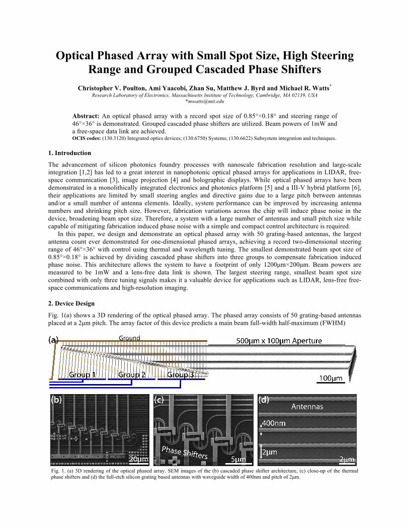
Fig. 1(a) shows a 3D rendering of the optical phased array. The phased array consists of 50 grating-based antennas placed at a 2µm pitch. The array factor of this device predicts a main beam full-width half-maximum (FWHM)
Fig. 1. (a) 3D rendering of the optical phased array. SEM images of the (b) cascaded phase shifter architecture, (c) close-up of the thermal phase shifters and (d) the full-etch silicon grating based antennas with waveguide width of 400nm and pitch of 2µm.
intensity spot size of 0.80° in the lateral direction and grating lobes at ±51° when the main beam is centered at 0°. Each antenna is evanescently coupled off a common bus waveguide. Between each coupler, a thermal phase shifter is placed to create a cascaded phase shifting architecture [Fig. 1(b,c)]. Each phase shifter has a 2π phase shift occurring at 12V with a resistance of 5.7kΩ. Unlike previous work [7], the cascaded phase shifters are grouped into three distinct electrical signals in order to achieve fine tuning of the beam to account for any phase noise in the device due to fabrication errors. It also allows for the phased array to act as three separate phased subarrays, each with its own beam controlled by separate group voltages. For beam steering applications with a single or few main beams using optical phased arrays, grouped cascaded phase shifters allow for a linear phase ramp in the antennas without complex individual antenna phase control, simplifying system control for a large number of antennas. Besides, additional control groups allow for finer beam control at the cost of more input signals to the system. However in this work, only three groups are needed to achieve a near diffraction limited spot size for 50 antennas. The antenna length is 500µm and is designed using finite-difference time-domain simulations to emit uniformly at 0° at 1550nm. The gratings are formed by a full etch of the silicon waveguide [Fig. 1(d)]. Utilizing a full etch over a ridge etch mitigates the risk of over or under etching the waveguide which is detrimental to uniform emitting long antennas. Polycrystalline silicon overlays can reduce this risk [8] but are not available in this fabrication process. The element factor of this antenna predicts a 0.16° FWHM intensity confinement along the antenna direction.
3. Device Characterization
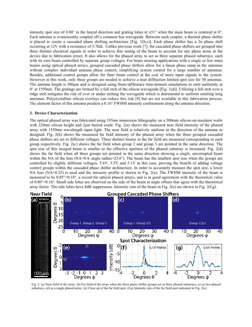
The optical phased array was fabricated using 193nm immersion lithography on a 300mm silicon-on-insulator wafer with 220nm silicon height and 2µm buried oxide. Fig. 2(a) shows the measured near field intensity of the phased array with 1550nm wavelength input light. The near field is relatively uniform in the direction of the antenna as designed. Fig. 2(b) shows the measured far field intensity of the phased array when the three grouped cascaded phase shifters are set to different voltages. Three distinct beams in the far field are measured corresponding to each group respectively. Fig. 2(c) shows the far field when group 2 and group 3 are pointed in the same direction. The spot size of this merged beam is smaller as the effective aperture of the phased subarray is increased. Fig. 2(d) shows the far field when all three groups are pointed in the same direction showing a single, uncorrupted beam within the NA of the lens (NA=0.4, angle radius=23.6°). The beam has the smallest spot size when the groups are controlled by slightly different voltages, 5.6V, 5.5V and 5.1V in this case, proving the benefit of adding voltage control groups within the cascaded phase shifter architecture. In order to accurately measure the spot size, a lower NA lens (NA=0.25) is used and the intensity profile is shown in Fig. 2(e). The FWHM intensity of the beam is measured to be 0.85°×0.18°, a record for optical phased arrays, and is in good agreement with the theoretical value of 0.80°×0.16°. Small side lobes are observed on the side of the beam at angle offsets that agree with the theoretical array factor. The side lobes have 8dB suppression. Intensity cuts of the beam in Fig. 2(e) are shown in Fig. 2(f,g).
Fig. 2. (a) Near field of the array. (b) Far field of the array when the three phase shifter groups act as three phased subarrays, (c) as two phased subarrays, (d) as a single phased array. (e) Close up of the far field spot. (f-g) Intensity cuts of the far field spot indicated in Fig. 2(e).

Fig. 3. (a) Far field of the array at different thermal and wavelength tuning values. (b) Main beam and grating lobe output of the array seen with an IR card. (c) Free-space data link created with the phased array as a transmitter and a photodetector placed 1m away.
Fig. 3(a) shows the far field of the device when steered using both thermal and wavelength tuning. Thermal tuning only steers in the lateral, ψ, direction while wavelength tuning primary steers in the antenna direction, θ, but also slightly in the lateral direction because of the inherent optical path length mismatch in the cascaded phase shifters. With thermal steering using 0-1.2W electrical tuning power, and wavelength tuning from 1454nm to 1641nm, we achieved a steering range of 46°×36° which is a record for optical phased arrays.
Fig. 3(b) shows the output of the phased array when an IR card is placed adjacent to it. A strong main and grating lobe are clearly visible. Another grating lobe on the other side of the main lobe is blocked by the electrical tuning probe, and therefore is not captured by the card. The grating lobes have similar powers to the main beam because of imperfection in the design of the antennas, which can be mitigated simply by increasing the antenna width [9] from 400nm to 550nm. Despite strong grating lobes, the power in the main beam was measured to be 1mW, limited only by the laser input power and the coupling efficiency of silicon inverse-taper edge-coupler.
With current device specifications, a lens-free free-space data link can be easily created. We modulated the input laser signal with a PRBS at 1Mbps using an external LiNbO3 modulator and transmitted the data through the phased array to free-space. The output from the phased array evolved into a beam size of ~1.5cm×0.3cm after one meter and was received by an InGaAs photodetector. Fig. 3(c) shows the signal captured by the photodetector, where data speed was mainly limited by the photodetector used in the experiment. This is the first demonstration of a lens-free transmitter free-space optical data link using a phased array. Farther distances could be enabled by using a lens at the photodetector for more efficient power collection.
4. Conclusions
A 50 element optical phased array with grouped cascaded phase shifters has been demonstrated within silicon photonics. Grouped cascaded phase shifters allowed for simplified control while having a record number of elements in a one-dimensional phased array in a compact 1200µm×200µm chip area. The phased array has a spot size of 0.85°×0.18° and steering range of 46°×36°, bests for one-dimensional optical phased arrays. Finally, with moderate beam output powers on the order of 1mW, this phased array can be used for applications such as data communication and LIDAR. This work was supported by the Defense Advanced Research Projects Agency (DARPA) E-PHI program under Grant No. HR0011-12-2-0007. The authors thank Dr. Joshua Conway for helpful discussions.
References [1] J. Sun, et al., Nature, 493, 195 (2013). [2] E. Timurdogan, et al., in OFC 2015 paper Th5B.8. [3] W.S. Rabinovich, et al., Proc. SPIE 9354, 93540B (2015). [4] F. Aflatouni, et al., Opt. Exp. 23, 21012 (2015). [5] H. Abediasl and H. Hashemi, Opt. Exp. 23, 6509 (2015). [6] J.C. Hulme, et al., Opt. Exp. 23, 5861 (2015). [7] A. Yaacobi, et al., Opt. Lett. 39, 4575 (2014). [8] D. Kwong, et al., Opt. Lett. 39, 941 (2014). [9] J.K. Doylend, et al., in OFC 2012 paper OM2J.1.