oscillator far-from-carrier phase noise reduction via nano
TRANSCRIPT
OSCILLATOR FAR-FROM-CARRIER PHASE NOISE REDUCTION VIA NANO-SCALE GAP TUNING OF MICROMECHANICAL RESONATORS
Mehmet Akgul*, Bongsang Kim, Li-Wen Hung, Yang Lin, Wei-Chang Li, Wen-Lung Huang, Ilya Gurin, Ashkan Borna, and Clark T.-C. Nguyen
Department of EECS, University of California, Berkeley, Berkeley CA, USA ABSTRACT
Substantial improvements in the far-from-carrier phase noise of oscillators referenced to stand-alone (as opposed to arrayed) capacitively transduced micromechanical disk resonators have been attained via the use of atomic layer deposition (ALD) to tune the electrode-to-resonator capa-citive gaps. Specifically, ALD of about 30nm of hafnia (HfO2) onto the surface of a released 60-MHz microme-chanical disk resonator to reduce its effective resonator-to electrode gap size from 92nm to 32nm provides an increase in power handling leading to more than 15-20dB reduction in the far-from-carrier phase noise of an oscillator refe-renced to this resonator. This ALD-enabled nano-scale gap tuning provides a simple and effective method to satisfy increasing demands for higher short-term stability in fre-quency references for electronic applications.
KEYWORDS
MEMS resonator, oscillator phase noise, atomic layer deposition, capacitive transducer
INTRODUCTION
With measured on-chip Q’s exceeding 150,000 at VHF and 15,000 at UHF, surface-micromachined capacitively transduced micromechanical disk resonators have already combined with properly-designed sustaining circuits to achieve phase noise marks commensurate with the refer-ence oscillator specifications required by the GSM cellular phone standard [1]. Specifically, GSM demands phase noise < -130dBc/Hz at 1 kHz offset from a 13-MHz carrier, and <-150dBc/Hz at far-from-carrier offsets. In satisfying these specs, the sheer Q of a capacitively transduced mi-cromechanical resonator easily makes the close-to-carrier number. The far-from-carrier number, on the other hand, is much less dependent on Q and rather relies more on the power handling capability of the resonator, which for ca-pacitive transduction is smaller than that of quartz crystals.
To overcome the power handling deficiencies of capa-citively transduced disks, [2] mechanically coupled many disks into an array composite resonator that behaved like a single high-Q resonator, but with a power handling capa-bility larger than that of a single resonator by a factor equal to the number of resonators used in the array. The solution of [2] comprises a mechanical circuit approach to raising power handling, so requires no changes in technology to achieve the needed performance. Arguably, such a circuit approach is perhaps the most elegant solution to the
far-from-carrier phase noise issue for commercial wireless needs. However, another method to raise the current han-dling ability of a capacitively transduced micromechanical resonator is to reduce its electrode-to-resonator gap spacing, which essentially provides it with a more efficient elec-tromechanical transducer.
Pursuant to investigating the efficacy of this approach, this work explores the use of ALD gap-filling methods [3] to reduce gaps towards a 15-20dB improvement in the far-from-carrier phase noise of an oscillator referenced to a micromechanical disk resonator. Although impressive, this figure comes at the expense of the close-to-carrier phase noise, which ends up suffering from 1) a lower Q caused by ALD; and 2) noise aliased by the larger nonlinearity arising from smaller electrode-to-resonator gap spacing. Before delving in, some review of phase noise theory is in order.
OSCILLATOR PHASE NOISE
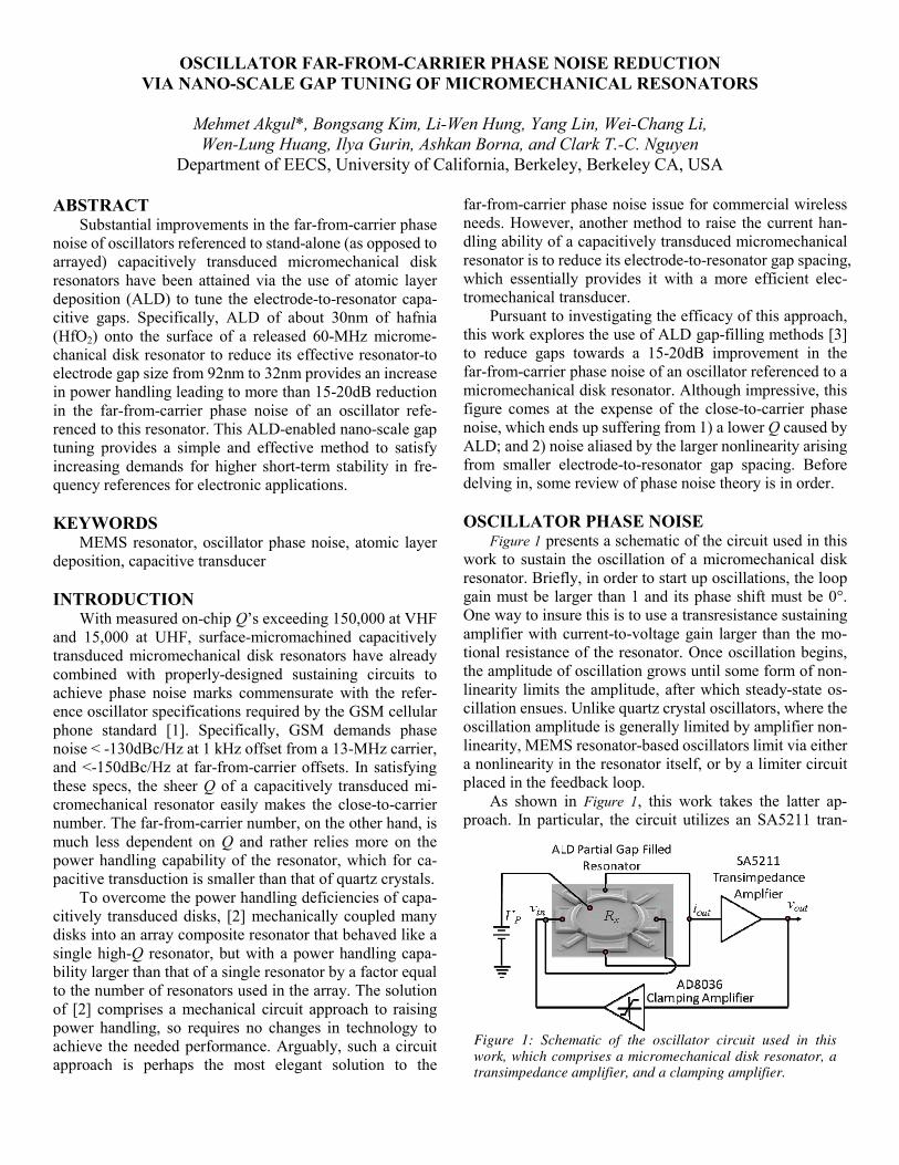
Figure 1 presents a schematic of the circuit used in this work to sustain the oscillation of a micromechanical disk resonator. Briefly, in order to start up oscillations, the loop gain must be larger than 1 and its phase shift must be 0°. One way to insure this is to use a transresistance sustaining amplifier with current-to-voltage gain larger than the mo-tional resistance of the resonator. Once oscillation begins, the amplitude of oscillation grows until some form of non-linearity limits the amplitude, after which steady-state os-cillation ensues. Unlike quartz crystal oscillators, where the oscillation amplitude is generally limited by amplifier non-linearity, MEMS resonator-based oscillators limit via either a nonlinearity in the resonator itself, or by a limiter circuit placed in the feedback loop.
As shown in Figure 1, this work takes the latter ap-proach. In particular, the circuit utilizes an SA5211 tran-
Figure 1: Schematic of the oscillator circuit used in this work, which comprises a micromechanical disk resonator, a transimpedance amplifier, and a clamping amplifier.
simpedance amplifier with a transresistance gain of 14kΩ, together with an AD8036 clamping amplifier that clamps the voltage applied to the micromechanical disk resonator to a specifiable value, thereby limiting the oscillation am-plitude of the overall oscillator.
Given that the main function of an oscillator is to provide a very distinct and stable frequency, the output of a perfectly ideal oscillator should in principal be a delta function in frequency domain, where all energy is at one and only one frequency. However, in practice, noise from the electronics or the resonator element superposes itself onto the output sinusoid, generating power at frequencies adjacent to the output frequency as shown in Figure 2. This adjacent power is considered undesired noise. In general, this noise comprises both amplitude and phase components. However, when the oscillation amplitude is limited at a constant level during steady state operation, e.g.,, by the limiter in circuit of Figure 1, only phase noise remains.
Leeson’s model describes the oscillator phase noise as the single-side band noise-to-carrier power ratio at an offset frequency Δf from the oscillator’s carrier frequency fo via the expression [6]
{ } ⎟⎟
⎠
⎞
⎜⎜
⎝
⎛
⎟⎟
⎠
⎞
⎜⎜
⎝
⎛+⎟⎟
⎠
⎞⎜⎜⎝
⎛Δ
=Δ 14
1log102
2 ff
QPTFkfL b (1)
where kb is the Boltzmann constant; T is the absolute tem-perature in Kelvin; F is the noise factor of the sustaining amplifier; Q is the loaded quality factor of the resonator; and the oscillator carrier power P is given by
xin RvP /2≈ (2)
where vin is the voltage applied to the resonator input and RX is the resonator motional resistance. Rx is given approx-imately by [7]
( ) Qd
VAmR
Poo
orx
4
2 ⋅=ε
ω (3)
where A and d are the electrode-to-resonator overlap area and gap spacing, respectively; mr is the equivalent dynamic mass of the disk; ωo is the radian resonance frequency of the disk; VP is the dc-bias voltage; εo is the permittivity of air; A
is the electrode-to-resonator overlap area; and d is the electrode-to-resonator gap spacing. Assuming that the first term in the product in (1) remains constant, and given that the clamping amplifier sets vin constant, (2) can be rewritten
4/ dQP ∝ (4)
Plugging (4) into (1), the oscillator far-from-carrier phase noise (when Δf is large) becomes,
⎟⎟⎠
⎞⎜⎜⎝
⎛⋅
=⎟⎠⎞
⎜⎝⎛=Δ 4/
log10log10)(dQc
TFkPTFkfL bb (5)
where “c” is a constant. Using reduction scale factors, the change in far-from-carrier phase noise can be expressed as
)log(40)log(10 dQ nnL +−=Δ (6)
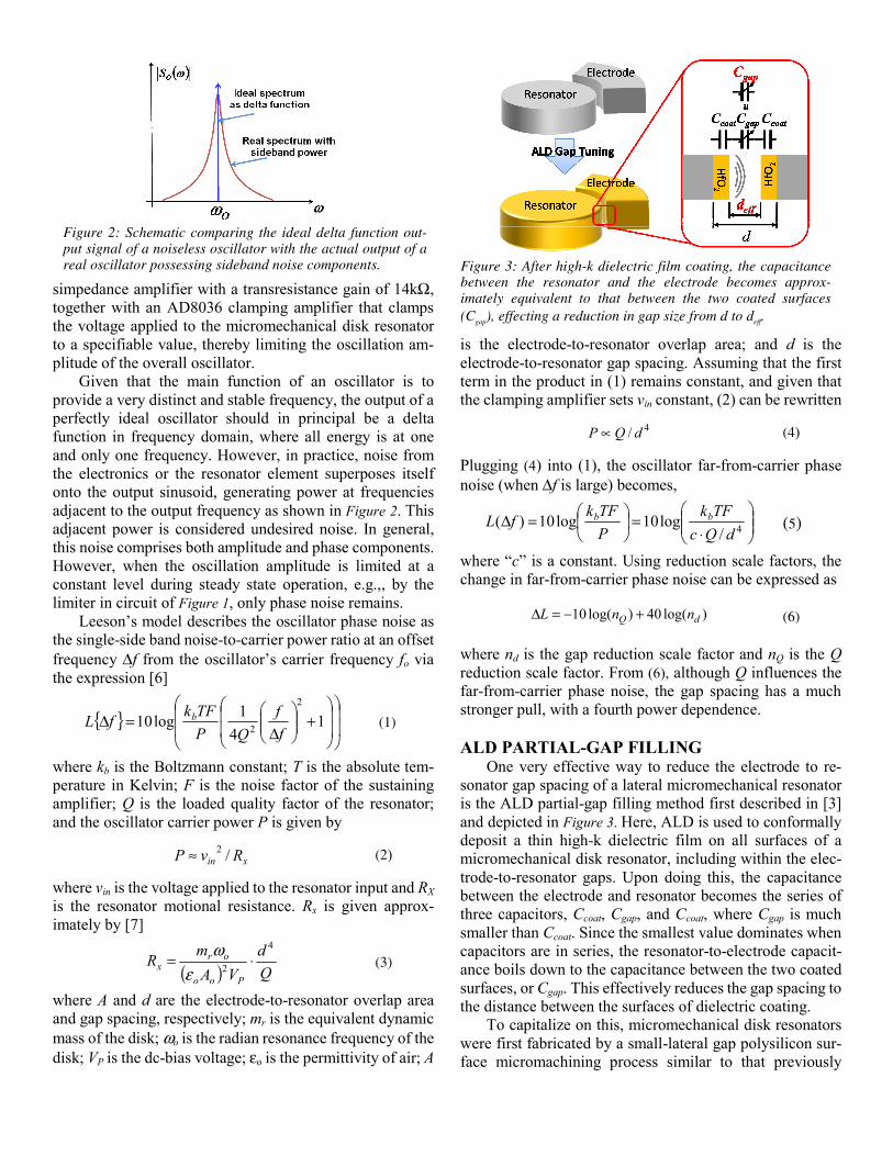
where nd is the gap reduction scale factor and nQ is the Q reduction scale factor. From (6), although Q influences the far-from-carrier phase noise, the gap spacing has a much stronger pull, with a fourth power dependence. ALD PARTIAL-GAP FILLING
One very effective way to reduce the electrode to re-sonator gap spacing of a lateral micromechanical resonator is the ALD partial-gap filling method first described in [3] and depicted in Figure 3. Here, ALD is used to conformally deposit a thin high-k dielectric film on all surfaces of a micromechanical disk resonator, including within the elec-trode-to-resonator gaps. Upon doing this, the capacitance between the electrode and resonator becomes the series of three capacitors, Ccoat, Cgap, and Ccoat, where Cgap is much smaller than Ccoat. Since the smallest value dominates when capacitors are in series, the resonator-to-electrode capacit-ance boils down to the capacitance between the two coated surfaces, or Cgap. This effectively reduces the gap spacing to the distance between the surfaces of dielectric coating.
To capitalize on this, micromechanical disk resonators were first fabricated by a small-lateral gap polysilicon sur-face micromachining process similar to that previously
Figure 3: After high-k dielectric film coating, the capacitance between the resonator and the electrode becomes approx-imately equivalent to that between the two coated surfaces (Cgap), effecting a reduction in gap size from d to deff.
Figure 2: Schematic comparing the ideal delta function out-put signal of a noiseless oscillator with the actual output of a real oscillator possessing sideband noise components.
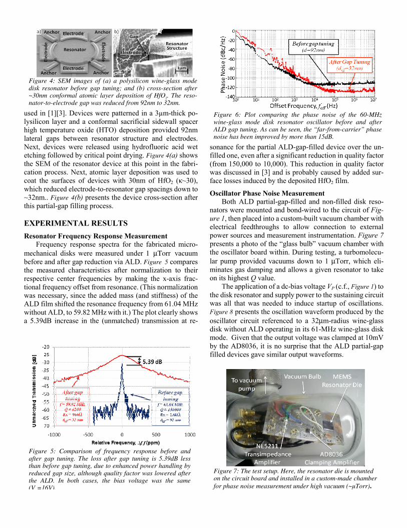
Figure 4: SEM images of (a) a polysilicon wine-glass mode disk resonator before gap tuning; and (b) cross-section after ~30nm conformal atomic layer deposition of HfO2. The reso-nator-to-electrode gap was reduced from 92nm to 32nm.
used in [1][3]. Devices were patterned in a 3µm-thick po-lysilicon layer and a conformal sacrificial sidewall spacer high temperature oxide (HTO) deposition provided 92nm lateral gaps between resonator structure and electrodes. Next, devices were released using hydrofluoric acid wet etching followed by critical point drying. Figure 4(a) shows the SEM of the resonator device at this point in the fabri-cation process. Next, atomic layer deposition was used to coat the surfaces of devices with 30nm of HfO2 (κ~30), which reduced electrode-to-resonator gap spacings down to ~32nm.. Figure 4(b) presents the device cross-section after this partial-gap filling process.
EXPERIMENTAL RESULTS Resonator Frequency Response Measurement
Frequency response spectra for the fabricated micro-mechanical disks were measured under 1 μTorr vacuum before and after gap reduction via ALD. Figure 5 compares the measured characteristics after normalization to their respective center frequencies by making the x-axis frac-tional frequency offset from resonance. (This normalization was necessary, since the added mass (and stiffness) of the ALD film shifted the resonance frequency from 61.04 MHz without ALD, to 59.82 MHz with it.) The plot clearly shows a 5.39dB increase in the (unmatched) transmission at re-
sonance for the partial ALD-gap-filled device over the un-filled one, even after a significant reduction in quality factor (from 150,000 to 10,000). This reduction in quality factor was discussed in [3] and is probably caused by added sur-face losses induced by the deposited HfO2 film.
Oscillator Phase Noise Measurement Both ALD partial-gap-filled and non-filled disk reso-
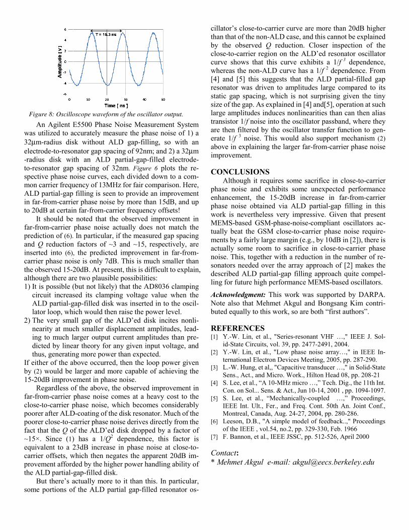
nators were mounted and bond-wired to the circuit of Fig-ure 1, then placed into a custom-built vacuum chamber with electrical feedthroughs to allow connection to external power sources and measurement instrumentation. Figure 7 presents a photo of the “glass bulb” vacuum chamber with the oscillator board within. During testing, a turbomolecu-lar pump provided vacuums down to 1 μTorr, which eli-minates gas damping and allows a given resonator to take on its highest Q value.
The application of a dc-bias voltage VP (c.f., Figure 1) to the disk resonator and supply power to the sustaining circuit was all that was needed to induce startup of oscillations. Figure 8 presents the oscillation waveform produced by the oscillator circuit referenced to a 32μm-radius wine-glass disk without ALD operating in its 61-MHz wine-glass disk mode. Given that the output voltage was clamped at 10mV by the AD8036, it is no surprise that the ALD partial-gap filled devices gave similar output waveforms.
Figure 5: Comparison of frequency response before and after gap tuning. The loss after gap tuning is 5.39dB less than before gap tuning, due to enhanced power handling by reduced gap size, although quality factor was lowered after the ALD. In both cases, the bias voltage was the same (VP=16V).
Figure 6: Plot comparing the phase noise of the 60-MHz wine-glass mode disk resonator oscillator before and after ALD gap tuning. As can be seen, the “far-from-carrier” phase noise has been improved by more than 15dB.
Figure 7: The test setup. Here, the resonator die is mounted on the circuit board and installed in a custom-made chamber for phase noise measurement under high vacuum (~µTorr).
An Agilent E5500 Phase Noise Measurement System was utilized to accurately measure the phase noise of 1) a 32μm-radius disk without ALD gap-filling, so with an electrode-to-resonator gap spacing of 92nm; and 2) a 32μm -radius disk with an ALD partial-gap-filled electrode- to-resonator gap spacing of 32nm. Figure 6 plots the re-spective phase noise curves, each divided down to a com-mon carrier frequency of 13MHz for fair comparison. Here, ALD partial-gap filling is seen to provide an improvement in far-from-carrier phase noise by more than 15dB, and up to 20dB at certain far-from-carrier frequency offsets!
It should be noted that the observed improvement in far-from-carrier phase noise actually does not match the prediction of (6). In particular, if the measured gap spacing and Q reduction factors of ~3 and ~15, respectively, are inserted into (6), the predicted improvement in far-from- carrier phase noise is only 7dB. This is much smaller than the observed 15-20dB. At present, this is difficult to explain, although there are two plausible possibilities: 1) It is possible (but not likely) that the AD8036 clamping
circuit increased its clamping voltage value when the ALD partial-gap-filled disk was inserted in to the oscil-lator loop, which would then raise the power level.
2) The very small gap of the ALD’ed disk incites nonli-nearity at much smaller displacement amplitudes, lead-ing to much larger output current amplitudes than pre-dicted by linear theory for any given input voltage, and thus, generating more power than expected.
If either of the above occurred, then the loop power given by (2) would be larger and more capable of achieving the 15-20dB improvement in phase noise.
Regardless of the above, the observed improvement in far-from-carrier phase noise comes at a heavy cost to the close-to-carrier phase noise, which becomes considerably poorer after ALD-coating of the disk resonator. Much of the poorer close-to-carrier phase noise derives directly from the fact that the Q of the ALD’ed disk dropped by a factor of ~15×. Since (1) has a 1/Q2 dependence, this factor is equivalent to a 23dB increase in phase noise at close-to- carrier offsets, which then negates the apparent 20dB im-provement afforded by the higher power handling ability of the ALD partial-gap-filled disk.
But there’s actually more to it than this. In particular, some portions of the ALD partial gap-filled resonator os-
cillator’s close-to-carrier curve are more than 20dB higher than that of the non-ALD case, and this cannot be explained by the observed Q reduction. Closer inspection of the close-to-carrier region on the ALD’ed resonator oscillator curve shows that this curve exhibits a 1/f 3 dependence, whereas the non-ALD curve has a 1/f 2 dependence. From [4] and [5] this suggests that the ALD partial-filled gap resonator was driven to amplitudes large compared to its static gap spacing, which is not surprising given the tiny size of the gap. As explained in [4] and[5], operation at such large amplitudes induces nonlinearities than can then alias transistor 1/f noise into the oscillator passband, where they are then filtered by the oscillator transfer function to gen-erate 1/f 3 noise. This would also support mechanism (2) above in explaining the larger far-from-carrier phase noise improvement. CONCLUSIONS
Although it requires some sacrifice in close-to-carrier phase noise and exhibits some unexpected performance enhancement, the 15-20dB increase in far-from-carrier phase noise obtained via ALD partial-gap filling in this work is nevertheless very impressive. Given that present MEMS-based GSM-phase-noise-compliant oscillators ac-tually beat the GSM close-to-carrier phase noise require-ments by a fairly large margin (e.g., by 10dB in [2]), there is actually some room to sacrifice in close-to-carrier phase noise. This, together with a reduction in the number of re-sonators needed over the array approach of [2] makes the described ALD partial-gap filling approach quite compel-ling for future high performance MEMS-based oscillators.
Acknowledgment: This work was supported by DARPA. Note also that Mehmet Akgul and Bongsang Kim contri-buted equally to this work, so are both “first authors”. REFERENCES [1] Y.-W. Lin, et al., "Series-resonant VHF …," IEEE J. Sol-
id-State Circuits, vol. 39, pp. 2477-2491, 2004. [2] Y.-W. Lin, et al., "Low phase noise array…," in IEEE In-
ternational Electron Devices Meeting, 2005, pp. 287-290. [3] L.-W. Hung, et al,, "Capacitive transducer …," in Solid-State
Sens., Act., and Micro. Work., Hilton Head 08, pp. 208-21 [4] S. Lee, et al., “A 10-MHz micro …,” Tech. Dig., the 11th Int.
Con. on Sol... Sens. & Act., Jun 10-14, 2001 , pp. 1094-1097. [5] S. Lee, et al., “Mechanically-coupled …,” Proceedings,
IEEE Int. Ult., Fer., and Freq. Cont. 50th An. Joint Conf., Montreal, Canada, Aug. 24-27, 2004, pp. 280-286.
[6] Leeson, D.B., "A simple model of feedback..," Proceedings of the IEEE , vol.54, no.2, pp. 329-330, Feb. 1966
[7] F. Bannon, et al., IEEE JSSC, pp. 512-526, April 2000
Contact: * Mehmet Akgul e-mail: [email protected]
Figure 8: Oscilloscope waveform of the oscillator output.