· pdf filelaxation oscillator similm to the multivibrotor in operation. whereas the...
TRANSCRIPT

ELECTRONIC CIRCUITS NAVSHIPS
SECTION 20
TIME-DELAY CIRCUITS
PART A. ELECTRON-TUBE CIRCUITS
PHANTASTRON CIRCUITS. ~~. ihe phmtastron-type circuit i s considered to be 0 re-
laxation oscillator similm to the multivibrotor in operation. Whereas the multivibrato~ derives i ts timing waveform from an R-C circuit, the phontastron uses o basic Miller-type sweep generatoi to geneiote a lineai timing waveform, rother than the exponential waveform developed by the R-C circuit of the muluvibrator. Thus, the output waveism 1s c lineor function of tne lnout Icantroli v n l r n r ? ~ , nnA tho !irrin; ttlt- i k y is irr)psovd.
The phantastron i s ussally triggered on by the leadizg edge of u qaung or trigger paise applied to the suppressor oiid ior to the piotei of c penrod-, ~ n d is shut a!! hy zr. lntrrnolly generated waveform. It con also be controlled by the trailing edge of the gate or trigger. It i s basically o single pentodetype tube (pentagrid tubes are olso used), witt~ two or three diodes arianged to control lmearity, turn- on or tum-o!f tine, and operating level. Two types of phontastron circlilts are used- the screen-coupled type and the cothode-couple': !ype. The screen-coupled circuit uses on internally generated waveform, generoted in the screen
circuit to control the suppressor electrode after the action i s initiated by an input trigger. The cathodesoupled cir- cuit ut~lizes an internally generated woveform developed oiioss u resistor in h e coinode arcuit to control aperotioc. Eoth clrcuits are classed a s the slow-recovery type and use the basic Miller plate-to-qiid feedbock to provide reasonablv iost !urnen ond turn-of! tine. The fost-recovery type cir- cuit uses n seporate cathode follower to help speed up operation and provlie a shorter recovery time.
The relationship ktweeo tihe scieer;coup!ei. and cathode mspled C I ~ C C I ~ S i5 ona!oqms to thoi 01 lha viurero-qrid and cathodesoupled multivibrators. Although the screen coupled phonast:on i s considered to have the best timins . . occurocy, the cothode-coupled circuit has other advantages. For example, it does not require onegatlve supply and can provide both positive andnegative outpgts, and it is clalmed t h t lor short ranqes tne linear~ty at the time rnodulotlon 1s
octuaily better.
BASIC PHANTASTRON CIRCUITS.
APPLICATION. The phofitastron circuit i s used to generate a rectanqulor
... , , -.. e i-.? . . , >weep, - wnose durarion is aimost dl-
rectiy proportional to a controi voltage. Because of i ts ex- ... 1ineorh.j ~ n d a i iu raq , tills woveiorrn is use: a s z
delayed !inn< p~!se, ;sii;!!r in i d o r o: dis;loy equipment. i~ 1s aiso used to produce time-delayed trigger pulses for synchronizing purposes and movable marker signals for d!spioy. to r example, it i s used os a time-modulcted pulse. to indicate antenna pos~tion at cny msan t c! rotatlon, or 2s o rmqe stroke o i 1~l ,y ~ a i ~ e r .
900,000.102 TIME DELAY CIRCUITS
CHARACTERISTICS. Operotion is similor to the operation of anultivibrator. Pulse width or delay vories linearly with the applied
control voltage. R q ~ i r e s on electron tube of the pentode or pentagrid
type. Outp~t can be :&ken !ioc the c o h d e , siieeil, or plate.
ond a i r y Lr either positive or negouve, as selected. Provides either o low-impedance or highimpedorce out-
put, determined by output mnnections. Moy be self-controlled or externally controlled.
CIRCUIT ANALYSIS. General. The operation of the phontastron circuit i s
L;;;: ;i. L?e ~ j c U: u iiiiirr-type iineor sweep leneratlr which uses o suppressoi-gated pentode. In the Miller linear sweep generator, the suppressa; grid i s notrnally biased (negative) to prevent plate current flow, while the screen C U S ~ ~ U C ~ S nea~liy. The grid is returned to HI through a resistor so !hot it is effectively at zero potential, and the cathode is qtounded. When opositlve gate i s applied to the SuDDresSOr, d a t e current flows and produces a v0ilor;e . . . . drop across the plote load resistor. This negativeswinging alate voltaue is fed back throuqh a small mwcitor to the 1 grid, and quickly drives the grid negative; thus, it mointiiins the plate current at a small value, and olso qreatly reduces . ~
the icreen current. Reduction of the heavy screen current produces a iarue positive swing on the screen, and the tube essentially remains in this condition, producing a positive screen gate. Meanwhile the plote current flows under con- ..-, s! the feedback voltage applied to tine q i d until no
further feedback i s produced. During this time the plate- current increase is linear, and the plate voltage continues to drop. (The normal discharge of C through R, would cause the current through the t u b to increase in on ex- ponential manner, thereby causing the plate voltaqe to drop sxponentiaily. However, my exponential chmge i s fed back to the grid 180 degrees out of phase with the normal discharge of C, thereby causing a linear increase in plote current.) At a p i n t a b u t 2 volts a b v e qowd, however, no further plate swing i s possible, and the screen again conducts heavlly, returning almost to the initial operating point. When the suppressor gole ends, t!e plate current i s cut off, the screen returns to its initial operatinu point. md . . !-e !;. :~3!). I: % :esm.ed .:.:er cocrc: c i the r.ex? .,._ .,..-::,. .-.. . . .c ..... 0 . 8 . a,..rnx:: cccws :ne x5:: Vi!.cr circait. Observe that the screen is not coupled, thot o separate bias source is osed for the suppressor, and tho! an external sweep gate i s necessary. These me the main ways in which it differs !rom the phantastron.
From the mrc~ i t actlo- desc:iSed p;evi;,s:y, it is c!ear that changing the oppl~ed plate voltaqe will deteirn~ne thepo~nt, and the time, ot which tne plate voltage "bottoms" (with respect to ih?!ea.?i~$ d g e c! t5.e in?;: ~ v i - ! ~ r r 3 aild the screen resumes control. Changing the vaiuesof feedback copoc>rm C and ;rid :esista: P. ,::ill ;!so ditnmine ihe time ..' . . .ation (by controlling tne speed of the gr~d-plate fee6 'mck action). b t ' h methods of controlling the time are used Ir! phontosrron c!rcuts.
ORIGINAL

ELECTRONIC CIRCUITS NAVSIIIPS 9'33. OW. 102 TIME DELAY CIRCUITS
L INPUT
4 --- --- ---
Miller Linear Sweep Generator
Circuit 0p.rotion. As mentioned previously, there are two Sasic types of phantastron circuits in use - the screew coupled and the cathodesoupled. ?he name i s derived from the manner in which the qate for the suppressor is obtained. Recall that in the Miller circuit a positive gate is developed on the screen during operatian; by coupling the screen to
operation. A migger pulse i s needed only to stort operation, because t u r ~ f f i s automatic. By inserting o cathode r e sistor between the cathode andground, a negative gate i s developed and used to control the the cathode-coupled phantastron. Each of these circuits will be discussed more thoroughly in the following paragraphs.
Screen-Coupled Circuit. A typical monostoble screen- coupled pentode circuit i s s h o w in the accompanying fig- ure. This circuit i s started by a positive trigger applied to the suppressor grid, and at the end of operation it returns to the initial starting condition, ready to repeat the cycle of operation when the next trigger arrives. The output taken from tne screen is o rectmyulor positive gate whose durotion, or length, i s controlled by R7. In the illustration, t u k V1 i s the basic phantasmon, ond diode V2 acts a s a triyyer in- jectdr and also a s a disconnecting diode to effectively isolate the trigger circuit after the action i s started. Diode V3 sets the maximum level of plate voltage as controlled by the position of R7, and, since the turn-off level is flxed, ~t effectively controls the time during which the circult produces the lmear gate or sweep, Operation occurs at the rote fixed by the discharge of C through R5. In some clr- cuifs R5 i s made variable to set the maximum time delay, ond R7 i s provided a s an external control to permit selection of the exact time duratlon required. Feedbck capacitor C provides regenerative feedbock from plate to grid, to allow quick response to any changes In the plate circuit. Cr;?
Boric Screen-Coupled Phantastron
acitoi Cl couples the positive gate from the screen to the suppressor, thereby holding the tube in a condition where plate current can flow.
Circuit operation con best be understood by referring to the waveforms developed in the tube elements shown in the following illustration, while reodlng the description of the circuit action. Three steps me involved in the clrcuit action--turn-on. linem sweeo develooment, md turn-off. . . Before initiation of action, the circuit i s resting with the d a t e current cut off. because a neqative voltage i s applied ;o the suppressor element through ~ 3 . Resistors ~ 1 , - ~ 2 , and R3 form a combined suppressor md screen grid voltage divider connected wtween B plus and C minus. The values are such that the screen i s positive and the suppressor i s sufficiently negative to cut off plate current. Since they are directly connected, b t h elements are d s coupled; also, through capacitor C l they ore a-c coupled. Therefore, both d s and a-c voltages appeorinq on one element also offect the other element. Since the cathode i s grounded and the grid i s connected through R5 to B+ , the grid remains near zero bios. Thus, although the plate current i s cut off. the screen current i s heavy. When a positive trigger i s applied to the plate of disconnecting diode VZ though coupling capacitor Co the diode conducts, md the positive trigger appears across R3 and 1s applied to the suppressor of V1. The trigger i s large enough to overcome the fixed negative bios and drive the suppressor positive. Therefore,
ORIGINAL


ELECTRONIC CIRCUITS N A V W I P S
1 - -lJ--n- OUTPUTS
Basic Cathode-Coupled Pharartron
zero, being held by diode V2 at a potential determined by the voltage divider (R1, R2, and R3) mnnected between B+ and ground, and the cathode i s positive with respect to the grid by approximately 1 or 2 volts. When the trigger is applied, it overcomes the bias between the suppressor and cothode, and plate current flows. The decrease in plate voltage, due to the flow of plate current, i s fed bock to the grtd through capocitot C, causing the tube current to de- crease and the cothode voltage to drop. This drop in cath- ode voltoge further deneases the bias between the suppress or and cothode, and plate current increases further. Since the total tube current is decreasing and the plote current i s increasing, the scieen cunent must decrease. This actlon i s regenerative, and plate current will jump from zero to o value determined by the tube characteristics. (Note that the bias between the cathode and suppressor is decreasing, which i s regenerative, causing the plote current to increose. The bias between the cathode andgrid i s increasing. T h ~ s oction i s degenerotive, which deneases the totol tube current. nerefore, there must be o point where these two effects are equal and the current will stabilize for a instant.) At this instant there i s no further change in plote voltage, ond the grid voltage increases in the positive di- rection at a rote determined by C and R5, since it i s re- turned to Ebb though resistor R5. This causes the plate cunent to increase. As the plate current incrmses, the plate voltage decreases, and this neqative change is coupl- ed through C to the grid. It can be seen that this signal i s degenerative, ond prevents the plote current from increasing rapidly. This onlon continues, providing a lineor sweep unt~l the plate voltogedrops to a level ot wh~ch i t can no lonqe: couse a r innease m piate current. At tius tine,
ORIGINAL 82 1
900,000.1Q?. TIME DELAY CIRCUITS
degenerative feedbock to the grid stops, and the grid will go in a positive direction more quckly. This causes an Increase in the totoi tube current, and thus on increase in cathode voitoqe, m increose in csthode-to-suppressor bias, and o decrease in plate anent. With the totol tube current incieosing and the plote current decreasing, the screen current must be mcreasing. It con k seen that the oction toking place i s regenerative, a s the plate will go positive, causing the grid to go positive, and the plate current will go rapidly to cutoff, leoving the tube in its pretriggered condition. The positive swing in the grid is limited by the "catching" diode, V2. Before the circuit i s ready for the next cycle of operation, capacitor C must recharge through R3, R2, V2, and R4. As in the screen-coupled phantostron, this circuit i s also ot the slow-recovery type.
As stated previously, when the phantostron i s triggered there i s a large drop in the screen current. Thls produces a positive waveform on the screen with a steep leading edge. As the tube cwrent gradually increases, producing the lin- ear sweep in the plote circuit, the screen current increases in the same manner, but by o smaller amount, in proportion to the plate current. The screen waveform will therefore de- crease linwrly by a small amount until plate current cutoff (described previously) i s rmched. At plote curient cutoff, the screen current inneases abruptly, causing a steep trail- ing edge. Negative overshoots at the trailing edge of the waveform will be limited by the oction of diode V2.
The resultant woveform across the cothode resistor can be visualized from the previous description of tube operation, by toking into account the changes in the totol tube current. This waveform will be a negotive gate with steep leading and trailing edges ond with the ilot portion falling off in amplitude ot a linear rote. Any positive oveishwt at the trailing edge will be limited by diodeV2.
As in the sneen-coupled phontoslron, resistor R 5 can be mode variable to set the maximum width or deloy. Rl is voriable, andis connected to the plate of VI through diode V3, thereby setting the level of plate voltage ot which the phantostron beginsits oction (when triggered). It can be seen that this will determine the amplitude and thus the duration of the plate woveform. R1 is usuolly an external control to vary the width or delay, and R5 can be an internal adjustment to set the maximum width or deloy.
In contrast to the screen-coupled phantastron, the cathode coupled phantostron has a smaller range of operation. The maximum plate crnplitude swinq of VL i s limited by the volue of the cothode resistor, in that "bottoming" of the plote voltage occurs at amore positive potentla1 than in the case ot the screen-coupled pnantastron.
FAILURE ANALYSIS.
and H3) or opm load resistors will orevent ooerutlon, as ~111 a faulty electron lute. Loss 3f ,"put trigger $?ill also reoier t5c circuit inoperotive. It is 3\50 p o i s l i l ~ Lor e x e s - sive b m i to rnke the clrcuit inoperotive oeczuse the trljcer O-PDIIIJIC i s not sufficient to overcome the bizs m i inltiote ooeratlon. Such 3 condltlon i s indicate.1 #hen on Input trlqqer con be seen on the suporessor wlth 21 nscilloscapr m i voltnqe opsears on 211 tube elements, but elther the

ELECTRONIC CIRWllS NAVWIPS rn,m.l@ grid or cathode voltage i s higher than normal. This i s most likely to occur in the screen-coupled circuit, where a neya- tiw fix supply i s employed with a common bleeder to obtain bias. Since the cathodemupled circuit develops its own bias, an excessive current drain or short-circuit condition would k needed to increase bias to the non-operatiny point.
DIS,-~ Ourpu.. D:stoit:~r, i s :;diccte,:ed b; a xox- lineor waveform or m inoccurate time delw. Linearity of sweep development i s the h s ~ c property of this circuit, with the mntrollinq elements k i n q the applied d-c mUo1 voltage md the RC time constant in the f&dhck circuit. Control voltage trouble may occur when the circuit uses a separate external control from a separate power supply, a s power suppiy iiuctuaiiwa rlur rosily chi i i ,~ ihe o3s;mk; level md hence the pulse duration. Failure of the p la t e cotchina diode is usuallv indicated bv lack of ccmtrol over the en&e ronge of operdticn, wherea; partial conU0l i s more likely to result from changing power supply voltage or a defective control. Chmge of time constant due to chonges in circuit values or to failure or pmtial shorting of the capacitor will change the rate ofoperation andhence the time delav. It should be most noticeable for the longer delay times. False Viggering due to the pickup of k l s e or stray pulses in the mntral cabllng (a remote units) may affect both the starting and stopping of the gate. If the disconnecting or triggering diode i s used, however, such pickup will affect cnly the start unless i t i s coupled to the suppressor through stray capacitance, and thls i s rather
point trouble in thls type of circuit ,unless on oscilloscope i s used to observe the waveforms at each electrode, because there are four h s i c types of trouble, namely, starlhg trouble, stopping tmuble, linearity, and recover/-time f d u r e
LOW Un.h!bl. Ourput. Low s m e n q a t e output indicates improper screen voltaye or current, which muy k caused by a defective electron t u k or a chanye in resistance value in the screen circuit. Low cofhcdeyate output in- dicates low cathode mrrent, which i s the sum of all element arrents, ond therefore may be due to any one of numerous causes. Usually a voltage check will indicate the defective companent. Unstability in lhe form of iitter ncr/ Le caused b pnwer supply voltaq~ fluctuations, noise, or false triqqers oicked up by unshielded wir~ng. An oscilloscope woveform check will reveal the cause of the unst3bility, which can !he? be rroced io iis srmice.
ORIGINAL
TIME DELAY CIRCUITS

ELECTRONIC CIRCUITS NAVSHI PS
FAST-RECOVERY PHANTASTRON CIRCUIT.
APPLICATIOHS. The fost-recovery phantastron circuit is used to generate
o linear sweep, or rectmgulor-wave output, whose duration i s directly proportional to a control voltage. Because of i t s extreme linear~ty and accuracy, the photastron output waveform i s used os a delayed timing pulse, to produce t i m e d e l ~ e d trigger pulses for synchromzing purposes, and movable marker signals for display.
CHARACTERISTICS. Operation is s~mllar to that of monostoble multivibrator. Pulse width or deloy varies linearly with the applied
control voltoge. Rewires an electron tube of the pentode or pentagrid
type. Circuit operation tum-on i s by application of negative
trigger or gate to the plate, or positive trigger or gate to the suppressor qrid; tum-off i s nutornotic by internally generated waveform.
Output can be token from the cathode, screen, or plate, and may be either positive or negative, a s selected.
Provides either o low-impedance or high-impedmce out- put, as determined by the output connections.
CIRCUIT 4N4LYSIS. General. The fost-recoveiy phantostron circuit i s con-
sidered to he o relaxation oscillator similar to the multi- vibrotor in operotion. 'Whereas the multivibrotor derives i ts timing from an exponential waveform developed by an R-C network, the phmtostron uses o boslc Miller-type sweep generator to produce a linear timing waveform. (The opern- tion of the bosic Miller linear sweep generator i s described in the discussion of Basic Phontastron Circuits presented earlier i n Section 20 of this Handbook.) The phmtastron is usually turned on by the application of a qoting or trigger pulse, a d i s turned off outomotically by an internoily generated waveform.
The ropid return to the stable operating condition at tum-off i s the bosic property of the fost-recovery phantastror. circuit. The rapid recovery i s accomplished by charging the feedback capacitor through the low cathodeto-plate con- duction resistonce of o cothode follower, rather than through the high-resistonce plate-load resistor of the phantastron. The effect of the ropid charge path i s to return the plate voltage of the phmtastron circuit to i ts stoblecondition level ~mmediotely in order to prepare the circuit, in a s short a time a s possible, ior the next Input trigger pulse. Although the cathode follower decreases the usable range of the con- trol wltoge md the linearity, it i s necessary in order to reduce the recovery time when long-durouon delays are desired. Mether the slow-recovery or fast-recovery phontostron circuit is used in a given application i s determined by the recovery time requirements; otherwise, the c i r c~ i t s function in the some manner md serve the same purpose. Both o positive ond a negative rectangular-wave output with well-defined leading edges may be obtoined
W67-000-0120 TIME DELAY CIRCUITS
from the phontostron, depending on whether the output connection i s made to the screen or cathode, respectively.
Circuit Operation. The occomponylng schematic illus- trates a typical pentode cathodecoupled fast-recovery
phmtostron circuit. ?he circuit i s turned on by application of a negotive trigger pulse to the plate; tumdff i s automauc by on internally qeneroted gate. Pentode tube VI i s the phantastron proper. This tube must hove the capability of providing two control elements; that is, the suppressor qrid must be capoble of performing the function of another control grid. A suitable tube lor use as a photostran i s the minioturetype 5721 pentode because of the sharp cutoil characteristic of i ts suppressor grid. Another suitable tube i s the pentode type 6AS6. A pentagrid tube such as the
ChlHODE & OUTPUT -
Fort-Recovery Cothodc-Coupled Phontartron
6SA7 can also be used 1n the phantastron circuit if certain modifications are incorporated in the circult design . (A basic pentagrid tube photastron multivibrotor circuit i s discussed in Section 8 of this Handbook.)
The diode-connected triode, V2, functions a s a trigger injector a s well a s a clamping diode for connolling the plate voltoge level and determining the duration of the output gate. The maximum value of operating plate voltage 1s clamped to a level determined by the settlng of potentiometer R 1 in the cathode of V2, and, slnce the tum-off level i s fined,
CHANGE 1

ELECTRONIC CIRCUITS NAVWIPS 0967-000-0120 TIME DELAY CIRCUITS
the setting of h i s potentiometer effectively controls the time dwinq which the circuit produces the linem gote or sweep. Triode V3 i s the cothode follower circuit through which feedback capacitor C2 i s rapidly charged in order to permit t+e phmtcstnn plote valtage to rapidly return to the moxrmum operating level determined by trigger injector and clamping diode V2. Although the illust~ation shows ....- ----.... ...- 2.. '>. xr- ,nu ~ s r u r u r s ~riuvcs lux r r und V.3, in prociicoi circuit applications a single twin-triode i s heq.uently used for economy of tubes.
Potentiometer R1 md resistors R2 md R3 form a volt- age divider from the positive voltage supply (+Ebb) to ground. The resistonce values are such that the positive voltage developed across resistor R3 i s less thm the wsitive voitage developed o m s s cotnode-blos and iwd resistor R6; thus, the suppressor grid i s effectively biased negative with respect to the cothode, md plate current i s a 1 off. As mentioned previously, the setting of the wiper arm of potentlometer RI establishes the voltage level at the phmtostron plate, thereby determining the gote length. Resistor R4 i s o decoupling resistor in the cathode of the trigger injector md clamping diode, V2. Resistor R5 is the phantastron ploteload resistor; R7 is the screen grid lard resistor, md R9 i s the cathodelaad and coupling resistor for the cathode follower circuit.
Resistor R8 returns the phmtostron control grld to the
\ pasitive voltage supply, setting the bias level that initially permits the screen grid to mnduct heavily. Operation of the % circuit occurs at the rate determined by the discharge of
?, feedkc& capacit3: C2 through resistor RE: in =me cir- cults this grid-return resistor, which usuoliy has o value exceedmg 1 meqohm, i s mode variable to set the maximum delay or pulse width of the output gate. The action of cothode follower V3 and copacitor C2 provides feedhack from the phantasvon plote to its grid, to allow rapid response to my chmqe in the plate vullage. Capacitor C1 couples the input trigger to the cathode of trigger injector md clamping diode V2; this trigger initiates (or tums on) the phantastron oction. Capacitors C3 m d C4 are the output couplina capacitors for the screen qrid md cathode, respectively; o psltive gate i s obtained irom the screen qrid, md a neqotivegate from the cathode. If desired, a linear sowtmth waveform con be obtmed from the plate of the phmtostron clrmit.
The followinq simplified schematic diogram shows the ch~rqe md discharge paths for cwautor C2. The chorge
I - A CHkRGE WTH I
I B DISCHARGE PATH - -
Charge md discharge Paths t o r Capacitor C2
path (part A of the illustration) i s from ground thmu& the phmtostrm cothode resistor, R6, ond the low cothodrte grid conductior, resistance of V l to the left side of the cc- pac~tor, and thm fmm the right side nf the capacitor t6:ougi
the Low cathode-teplote mnduction res is tace of the cathode follower md the positive voltage supply back to ground. This i s the fast-recovery charge path for copacitor C2. That is, when the plote voltage of the phmtostrm rises, as it does at the end of the gate, i s free to do so without the interference of my lumped copacitmce; tube interelectrode capacitance md stray wire capacitance are the only hinder- ..ces. p,,, .-. i" ,. 'LC ., C ~ - - ^ i l - uq",.r PUUL ." r., ui, -:-- 7.. rv*
ot this time, since it aosis t ; mainly of the !aw mn?lictici, ;esistm~ce of me ~ L h o d e fullowe:. P ,e discharge psih (part B of the illustration) for capacitor C2 is from its left s:de throuqh bins resistor RB wjd thc pos~tivr vultu~~c suppiy to ground, and then irom ground through the cathode load resistor, 89, of the cothode foliower to the ricjtlt sllJr
of the capacitor. The long 8-C time ar.stmt of this pati, causes copaator Ci to discharge at a ilnem rate during the time that screen current i s low (near cutoff) md the phantastron tube i s drawing heavy plote current.
The operotion of the fost--very phontostmn crcult can best be understood by referring to tQe preceding ck-

ELECTRONIC CIRCUITS NAVSHI PS
cuit illustrotions md the accompanying woveform illustration dunng the following discussion. Men voltoge is first opplied, the plate section i s in cutoff ond there i s heavy screen grid current. The conduction of screen current i s a result of the fact that the operating voltage on this elec- trode i s sufficiently positive to attract electrons emitted by the cathode os o result of the positive b u s on the control gnd (positive voltoge return to & through resistor RE): this permits the flow of cathode current at this time. The current through cathodebias resistor P6 produces o volt- age drop across this resistor. The positive potentiol of the
'0 'I '2 '3 '4
INPUT ~ E G E ~ ~ 1 1 Pvn1 -
I U T E CURRENT CONDUCTING
PLATE MLTAOE VI WARGE
('01 cur OFF 4 Li
MLTLDE VI
I I CITWDE WLT~GE + IDISC~UIDL I I
ACROSS R(i
(*I I
0
- 1 . 1 b I ( d l 1 1 1 I
Theorcticol Waveforms for Fost-Racovety Cathode- Coupled Phont.rtroo
top of ieslstor R6 is now greater than the positive potential ot the suppressor grid, which is obtained across voltoge divider resistor R3. A bias voltoge i s therefore established between the suppressor grid md the cothode: this bias i s sufficient to cut off the plate current while having no effect on the screen current.
Because there is no plate current, the plate voltoge rises to the level determined by the setting of potentiv meter R1 in the cothode of the trigger injector md clamping dlode, V2. This some positive plote voltoge i s also im- pressed on the cathode follower conuol grid, since this grid md the phantostron plote are electricoily identical. The cothode follower now conducts, and the flow of current through its cothodelood resistor, R9, develops a positive potennol at the top of this resistor. This positive potential is coupled through capacitor C2 to the control grid of the phantastron, where it further increases phmtostron con- duction. The positive potenticl on the phmtostron control
0967.000-0120 TIME DELAY CIRCUITS
grid also couses thisqrid to drow current and charge cc- pacltor C2 through the path described previously. Tne foregoing ocuon is instontmwus a d causes the phantos- tron to assume its stable state, as depicted during time interval o on the wavefotm illustrotion. The circuit remains in fhis condition (heavy screen current and plote current cut off) until o negative trigger i s opplied to the phontos- tron plate through trigger injector and clampling diode V2 M instont t,.
When the negative trigger (ein) is opplied through ca- pacitor C l to the cathode of V2, it forward-bioses the diode md permits plote current to flow. This current, in turn, causes an immediate drop in the plote voltage d e "eloped across plotelood resistor R5. The negativeping signal i s also on the grid of the cathode follower, V3, where it acts a s a bias to reduce the conduction through V3, thereby reducing the voltoqe drop across its cathode load resistor, Rg. ?he negotivegoing slgnol ot the top of resistor R9 i s coupled through capacitor C2 to the control grid of the phantastrm tube, V1, where it drives this grid sufficiently negative to reduce the conduction of the phontos-
tron. Since the phontastron cothode current i s reduced, the screen current is also reduced: thus o positivegoing volt- oae is produced at the screen nid. Throuah cathode . . follower action of the phmtastron circuit, the negotlve-going s~anol on its control arid i s coupled to the cothode, where it now reduces the bios betwee" the cathode md suppressor grid. With o decrease in this bias voltoge there i s on in- crease in plote current, resulting in o further drop in plate voltoqe. The action just descnbed i s cumulative and in- stont&eous. Thus, when the negative bigger i s opplied to the cathode of V2 at t,, there is m immediate fall in phontostron plate voltage md o shorp rise in plate current (the fall in plote voltoge i s fed to the grid through cathode follower V3 and copacjtor C2 drlving the control grid negv tive), there i s a shorp rise in screen wltoge md o decrease in screen current, md there i s o decrease in total cathode current ond a sharp deneasein cathode voltage. All of the voltoge relotionships ore depicted at t, on the waveform illustrotion.
The fact that the phontostrm plate current increases while the cathode current decreases i s possible because the screen current i s now decreasinq. Therefore, the rise in plote current results from the fact that the plate draws current which had previously gone to the screen grid. Thot is, the bias between the cathode and the suppressor grid i s decreasing, which is o regenerative action, causing the plote current to increase. Simultaneously, the bias between the cathode and the control grid i s increasing, wh~ch I S a degenerative action, causing the total tube current (md screen grid current) to decrease. The screen grid current
i s only reduced -not cut off completely: it i t were cut off completely, plate current would also be cut off md the c~rol i t would not function. Hence, there must be o point where the regenerative md degeneroave effects ore equal
and the current stabilizes for cn ins1or.t. Tnis is the instant (at t,, when the show drop in plote voltage ceases) ot which capacitor C2 begins its discharge action.
CHANGE l

ELECTRONIC CIRCUITS NAVSHI K 0967-00Q0120 TIME DELAY CIRCUITS
As capacitor C2 discharges during time interval b. I!
l a s e s electrons from i t s lef t side, in e l fect making this s i d e of the copacitor land the control grid of the phantastror.) more positive to reduce the bias between the control :rid m d the cathode. The reducr:on in control grid bias permits a heovler flow of piote current through the phontostron, which qraduolly roises the voltni]e drnp ncrnss cnthodebia; resistor R6 (ek waveform), a s illustrated dur~ng time in- intervol b. The rate of change 01 tube current 1s qoverned by the discharge rate of capacitor C2 through resistor RE. Thus, in dischorg~ng, the control grid s ide of copoc:tar C2 qrodually becomes more pasitive, causing or: increase in plate current; this produces 3 constont decrease ir plate voltage, whlch i s fpd hopk 1" !he :i:? !k%;!: :;::.G?,:
iuiiuwrr 'V3 m d capocltor CZ. The positive voltoge in- crement on the control qrid i s d w o y s s lqh t ly jrtater trim the nega t ivega~og plote slqnal i t produces: therelore, the nr!d ootentlnl qrali~lolly rises l"d tire ? l a c pa:irhiial uolly drops, as depicted by the respective mntrol grid (eql and plote (ep) waveforms during time inteivol b.
The action described durlng time interval b continues until the plate voltage becomes s o law (only o iew volts) that phmitostmn tube Vl can no longer anplily the changes in plate voltage. At t!;:~ instant, I,, copacitor C2 stops ?ischor~:nc wd tL.2 contial d r id is rouidiv drlven oosltlve. ~. . . causinq the tube current to increose a t o very lost rote. '!?e rapid rise of current through c o t h o d e b ~ o s resistor R6 produces o high positive potential on the cathode, which, in relauon to the positive patentla1 on !he suppressor qrid, 1s a bias suiilclent !a cut off plate curre-!. S!IC~ !hn :c:G! tube current 1s lncreaslng at this inston!, the nddltiono! c!lirent must flow in the screen zr:? circuit. 7hi. uctlan no,+; OccdrilrJ : s irgcnerotive. A s the plate volraqe, whose swlllg is limltrd by trigger lnjector and clamping diode V2, goes posltive because of piote current mta f i , the posltlve-
qcinq siqiral is cuupied through cathode ioliower V3 and co- pacitcr C2 to the phontostron mntrol qrid: this signal comes o further increose in tube current, thereby producrnq 0
highei voltage drop across cathode reslstor RE to increase the bias on the suppressor grid ond further cut o!! plate current. The p s l t i v e q o i n g mid 01 the phontostron draws current ond now ropidly charges copocitor C2 through the low cothode-to plote conduction resistance of the catbcdc follower. Thos, nt insfm! t,, th.e phm!ast;on i s rapidly l e i u r n r d ro it5 0nqlnai slobie stotc 3f piate rdrrent cutof! 2;; 1:;uxlmuni screen grid current, as iiiustrcted 3 ~ : : s ~ . timi ac i r r ru l c, u n t u me next t iqqer pulse at 1, again couses o cyc le of phantastron actlon.
A s mentlaned previously, when I ~ P phnnln-trm is tnscered (turned on) there i s o sudden drop in screen
- r ! . :::s produces 2 p o s l t i s e g ~ i i i j vu;ruye or, me ;;:eer, iri:h a s teep leodmQ edge (esa wav~forrri. A! <be tlrhr v r r e n t qrtldual!y increoses, pioducinq the linear drop ~n plate voltoge, the screen cllrrpnt !Icrecsrs ir. the SCK
-oa.-:. '.gt by a w c h srzcller mount . The scree,, wove- !::.?, ,hi!: t h ~ s decrr~se ilneorly by o small amount untjl ~ h - " -1.1 ...= puL,,L ub Y~. i t ec t i> rmt c ,~ ro f i (descr!bc? n r ~ ; : c ~ s i ? ! i s
reoched. At the instant of plate-current cutofl, sciem current lncreoses sharply, causing o sharp drop in screen ~ l t o q e , as depicted by the trailing edge of the esq volt- ""- s ~ ~ ~ . , ~ I - . - . ". ...., .L.. i s the w s i t i v e g o r e output woveform coupled through capocitor C3 to the screen output terminals. Thp r~su l t an ! r.eqo!i:.~qstc ou tpa . e i , !&en u ~ ~ o s s p h a n t a s t i o ~ ~ ~ ~ u i i i u d r i o a d resistor R6, i s coupled through capacitor C4 to h e cathode output terminals. Tnis negotwe- gote wnvclorm also has s teep leading and trolling edges, wlth the flat portion falling oi l in amplitude a t a lineor rote.
From the circuit actlon lus t described, i t i s evident that changlng the value of the valtnge opplied to the plote will dctermlne me polnt, and the time, ot which the plote ~i:cuqc ' ' ~ u L c , u ~ ~ ? ' , ,wltr, r -spen t o the time 3! ~ p p l i c z t i ~ i i of the input trigger. Potentiametdr A l 1s connected to the pnantastron plate through diode V2, thereby setting the level of plote v o i t q e a t which the phontastron begins i t s . r~ i l u l : when rrlggered. Changing the volue of either feed- tack copocitor C2 or grid resistor RE will dso offect the pulse width by controlling the rote of discharge of copacitor C2. For e x w p l e , increasing the volue of copac:tor C2 or resistor H8 will increose their R-C time constant, thereby cousing capiicltor C2 to discharge more slowly ond increase the width of the delay :ate. A decressc in the iiolue of either copac:tor C2 or resistor R8 will hove the oppasite e f fec t on the width of the delay gote. In some phantastron circults the grid resistor, RB in this case, i s made "mi- able s o as to control the maximum width of the delay gote. 'rYh~n mode varlohie the qri-? resisto: i s m8 iiotrtnul d -';~~::ent, . , , . , . . . witrreos parenrlometer HI i s usualiy an external control.
i i :I ;s cesired to obtaln several ronqes of delay with the phantastron, t h e mast sotisfactory method i s to leave tne value of the grid return resistor IRE) fixed and switch in different volues of copoci tmce for the feedback capacitor ,-7, , L-*,-~. , o , , ~ . ~ r u w r r wiii pio.u~de n iow-lmpedancn point for the switching ond minimize the e f fec t s of stroy wire capacitance, m addition to providing o fost- recove:? path. A disodvwttuge of using the cathode fol- loner in the phantostron i s that it increases the maximum error of tiit. clrcuir. Ordlnariiy, the phontastron linemity I S " h ! n ~ e i by !he !~ciia:k be t .~?en plule ~ n j control qria, which tends tc mointoin a constant discharge of the feed- back cilpucitor (C2i. Since the gain of the cathode follower . , . I S ~ P C S !Ion m!!.:. !b,p m m p e i ~ o t i a n is ::,>: 2s llncm G :
ivhen tne ieznwck occurs th:o:;qh rh? capx i to : 3i3nc. Hcwcvei. G s:irtbt error ( i l F p r ~ ~ i m ~ t e ! y 3 . I ;P~SKI z i ;ontiol voltage of 150 volts, lor example) con be tolerated ,?;+ep, i! i s nec+:;5,jry :c, ,u,I,,c? !+c :ecv>cFj :;;,c <i tiLL -,.-.,,, .... in. .-. .-.+ I -... <.-. eA2vtya. duvpu gale signois.
FA!L!!RE ANALISIS. No Output. 'The input triqgei should be checked wlth on
o ~ c i ! ! ~ s i ~ p c w i t e r m i n e whether 11 1s beinq applied to me ciicult ond whether it i s of the p i o p ~ i polarity and ~rzp!itb?e. L c l : o! 1; ~ c p u t triqgei a t Lile cati,odp nf tngqrr
, , . ." :n,:ert:,r ,?r!,3 L] :!!! ?;.?: 5:cc: ,/L ,-,>: :- ,~< ,?.: z2 :pcz :;TC!
CHANGE i 20-A-9

ELECTRONIC CIRCUITS NAVSHIPS
couplinq capacitor, Cl, or to failure of the external InpJt- triqqer source. It i s also possible fur o defectlwe trl7zer injector md cimlpinq diode tube, V2, as well as rr_-essive bias, to moke the circuit inopeiative: the ercezsl.,- I los will prevent the fixedatplitude i n p ~ t triq~er frcn over- m i n q this lcvel and initiaiinq the phont~s:rclr xtion. 'Tqe foreqoinq conditions are indicated :,her, or i l p ~ l tr17,:~r con be seen with an oscilloscope on the coihodp o! VZ md voltaqe appears on all tube elements, but rlther t5e 2hontastron control grid or cathode voltooe is ~ i m e r llhon ,om>ol. 'ibis i s most likely to occur ,*her i nc~at lve vol- loqe source is used ~ i t h u common bl~edei nct::orx to 00 tnin the Mos (as in a screen-coupled circuit). S ~ n i e :his za:i~odecaupled pcntodc circuit divelops its owr. h:s, an zxcess~ve current droin or short-c~rcuit condltior vmul be needed to increase the bias to the noropcrutina mint.
Failure of the positive voltoqe suuply, +Ebi., i r l l l :̂.s- mpt the operation oi the circuit, as hill on own cotkCle circuit of either the phontastron or the catho:!~ !oIIc:;er. With tubes installed in the circult, ti,? filan~ent, plate, screen, md suppressor qrid voltaqes should be neosure?. os well as the bias voltoqe developed ocross ph.cntastron cothode resistor R6, to dcteimlne whether the applied vol- toqes ore within tol~rarlce oi wtether an associated tlec- trcde resistor i s open. I1 feedtack copacitor C2 is o?en or c a t h d e follower V3 i s inoperoiive, there will tr no feedback siqnal to promote the phantcstron octlcn. An o x n output couplinq copacitor. C3 or C4, will p:event t i t output- gate siqnol from rwchinq the follow~nq stcoc.
Reduced Output. A reduction in output is zer;e:olly cmsed by a def~tivephantastron tube; ho?vrver, c la;; screen qate output con 0150 be causcd by o decrease in applied voltoqe or a chonqe in resistance value ir the screen circuit. Low cathode qate output indicztes lev)
cathode current, which i s the sum of all tube element c r - rents, md thus may be causcd by my ane of rlur,e:ous con- ditions (decreased tube conductonce, rejuced plate or screen voltoqe, rtc). Usually, a voltow deck will lacote the defective circuit and component. A l eaky cr ibcrted olutput couplinrl cwocitor, C3 or C4, ;lill ior~r a volta?e divider with the input resistor of the fo l low~n stone. if the input resistor of this next staqe is returned to 'jro1~n5 cr tc a neqative supply, the voltoqe ot the screen qrld or cothode will be reduced, ond the operotion of the stoze v:111 Re upset by the chonqe m voltoqe applled to its arid.
Distorted or Unstable Output. Dist~rtlon 1s in2lca:ed by o nonlinear wovefornl or un inaccurate time dcluy. Llneority and uccuracy of the output qote W O V E ~ O ~ T I de\r~lppmer,t is thebasic property of ihis circuit, wlti. the controllina elu- nlmts beintr the oppiied d i control io!tone and ti- 9-C time ca~sturit in thi. !iedhock circuit. Control vo1tc;e trouble may occur when thv circuit ,IS?:. a ccoarxte i.xte:n;l control from n srpcroti. powci :;upply, slnrc ;lv?ver suppl) fluciuoticns con I . O S ~ I V C ~ U T I O P the aoerctlnl lecel und. therefore, the oat? :i~rati011. A chonile ~n !:",P ;o?stnn: ? ~ e to circuit vulurs or to fei4twr-k cupccitcr in l l~ re or lcako~c wlli chmge the mteof aperatlon a n d , hmce, the a t ? lenqth; this shoul5 k most noticuubl~ for (i-c lanqer ?ate
0967-OW0120 TIME DELAY CIRCUITS
lengths. False triqgerinq due to pickup of noise or stray pulses in the control cablinq (on remote units) mw affect bath the turn-on and turn-off of the qatr. 'lhisinstability, or jitter, can ulso be caused by power supply fluctuations. An oscilloscope waveform check at eoch electrode i s usuolly the best method to checkinq for the cause of jitter, which c m then be traced to i ts source.
Incorr.ct Frsqumcr. The fost-rmvery phmtostron circuit has no components qaverninq the frequency oi its output gate siqnol; this frequenw is qovemed by the in- put triqger applied to the circuit. Therefor?, m y chonqe in the output gate frequency i s a result of improper operation of the trigger generating circuits.
ELECTROMECHANICAL (ACOUSTIC) DELAY LINES.
APPLICATION. An electmmechmical or sonic delw line provides a
mms of retarding the passaqe of o simol or wave for o predetermined length of time without distoitinq the onanal composition of the signal or wave. ' h i s !ype of delay line i s used in mmputers md in radar equipmmts such as movinq target indicators (Mn).
CHARACTERISTICS. Delay line acts a s a medium between electrical md
sound impulses. Delay line is composed of qumz crystal slabs md a mercury
mlumn. Amount of ume deloy depends on lmqth of mercurv
column. Time delay affected by temperature variations.
CIRCUIT ANALYSIS. G.o.rol. The elecuom&mical (amustic) delw line
utilizes the piezoelectric effect of o quartz crystal slab to mnvert any electncai lmpulses within a circuit to sonic impulses. These sonic impulses traverse a mlumn of mercury of specific lmqtk md ore reconverted to electrical impulses by another suortz c ~ s t a l slob at the opposite end of the mercury mlurnn. Tne overall effect i s a resultant decrease in velonty relat~ve to the velociw of elecnicd impulses Voveling an equivalent distance. Thereiore, by inneasing the length of the mermry mlumn, the lonqer the impulses will remain in the sonic state, and the greater will be the deloy of h e impulses.
CIRCUIT OPERATION A pictoriol representation of an acoustic delw line i s
shown i n the follawinq illustrotion. ' h e delay line consists of two qumtz crystol slabs ond o column of mercury in o cy- lindricalccntoiner between the two crystal slobs. Aselectri- cal impulses ore applied to the first crystal slab of the delay line, the piezoelectric effect associoted with wsta l l ine substances causes these impulses m be converted into mrrespondinq medimcol expmsions and controctlons. One of the expandng md mntroctinq surfaces of the cwstal mntacts the mercuw mlumn in such a way that these
CHANGE 2

ELECTRONIC CIRCUITS HAVSHIPS
mechm,ical or sonic vlbrohons ore mnducted h i o ~ i *ti
mlumn in th? some w0-f :+at el~ctronc Ore conduct~d ti;ou7h o wire. Sonic imoulses trove1 ot o considerablv lower sseed ?hm electncol irnpulscs ond bv incrcasino thc lcnot+ of the mercury mlumr the tlm? k t ? s req'.?r?d !c: h e :m:';1ses :3
travel i~om one en.: of ii.e !!:ereu.i mlurnn to t!!e otner te comes qruter. T!le mount o! hilie delw 13 pr~poril~nal io the ratio 01 h e vcloclty 01 sound I n mercury to t5c velcclty of electric~l impdlse; thiauin thc ajnducunq x ~ t c n d IL;~?
in the circuit, multipilcd times the lenqth of the meraw column.
INPUT
QUARTZ CRYSTAL
SLAB
Electromechonicol (Acoustic) Deloy Line
ilpurr rrucnlrr,> Uje r!rt ui tile nlrrcurv column, Lqe S O ~ C
vibrations arr canvritei to clectriccl whritlons nv c l c l n applyin. the sonic vibrations too cristal slab. Ths crystal, "" ."- .,.?. --.-*,., -"."".,. ...-" "",,,,"" ..,".,.. .. "- ".,~ -..,. *,,.,, ".: -",.." ...- ..., ...*..,.... *-." ,.... ,.,. plan? of the crystal in .wtildi sonlc 01 xechon:~~! :rnp~!ses can be applied or abtaln~d (whidi hoppens to be po:>rr;X- --!or tc: the plcne sliln: ,:!hi+ t n ~ i c i-p-!:ps n:? .-p~!:e? or obtained).
CROSS SECTIONAL VIEW OF CRYSTAL
X ---- - ELECTRICAL AXIS
Y ----- MECHANICAL STRESS AXIS
0967-WO-0120 TIME DELAY CIRCUITS
FAILURE ANALYSIS. Since *,i ::onic e l c v line i s o s indc component the
failure onalvsis ccn be simplified. If no simol is ohtained ot the cutpat of the oelw line md the Drwer simal i s applied s t k e !-?;t, h c mcrmry miqht havi leaked fron the qlincer ::i.?ci: i s iu;;ost..! to mntoin it. Another couseoi il n6-ur;tgs~t curl!itlun ir!oy he open cy-'ni ?- n cpstn! si-orti i :o t ie :!letulllc case contoininq it. It ,will not be :.eces:cr; t: ic:rr:lne whici~ part of the rielm, linp is ot fault, since 3 : : ~ defect mil mnke it necessary for the en- ti. .c .. .:~.3,; 1 I::.c :i i~ -<-l,?ei i.
A :~strr:e: eitc.t !I:,>; be due lo the ef!ect o! te::lperrr , " - , . ,;;.._ .-.- .-- ... -. : 8 c rc tk,c ?rloy ]in? is us-3. Ti r; . .r-- i . I-. - . . -. . r --,.- .hV." :? " n"""<L;,:*. *.-. .. .
~ .~ . : . ~ .... . ----. , .- " ?"--" ..... ",", ".>
crjstols n q ;,i :a:: XC:. :!I order to prpwnt or cnrn3ct h i s c~,st3ilt l e r n p e ~ ~ t ~ r e mmilorinq should be


ELECTRONIC CIRCUITS NAVSHIPS 900.W0.102
PART B. SEMICONDUCTOR CIRCUITS
Pat B of this s s t i o n i s reserve3 for semiconductor time delay circuits, which moy be included in another revision of this Handbok. ?!o semiconductor time dela? circuits ore discusse? in this issue.
ORIGINAL


ELECTRONIC CIRCUITS NAYSHIPS
PART C. ARTIFICIAL DELAY LINES
ELECTROMAGNETIC DELAY LINES.
APPLICATION. Artificial deloy lines of the electromagnetic type are
~ s e d to geniiote iect&r,ilg~lai pulse; of :id diiration (in radar receiver and transmitter appi~cat~onsj; to produce o rectangular woveform from o step function of voliaqe (as used in storting and deloy triggers for test equipment and video display units); to terminote o pulse produced by 3
regenerative device such os o blmking oscillator or multi- vibrnor (as used in radar, timing ci;cuits, ond computers); and to duplicate on existinq pulse at o later time (a simple r r ise i t time deloy). ! ~ P S P iines ore commoniy tisea ior many types of waveshaping and pulseforming applications.
CHARACTERISTICS. Provides a constont attenuotion 01 sijnai, aepending
upon materid and construction. Consists of a number of equal sections (or holf-sections)
of lumped capacitance and inductance, providing o definite deloy interval.
Provides a definite phase shift which can be repeated at speci!ic intervals.
Possesses on inherent characteristic (surge) impedance which must he matched to input and output circuits for proper operation.
Similar in operation to a real tiansmission line, but q:e't]y in size.
CIRCUIT ANALYSIS. tene.ol. Delay lines cre simple t i construct, re!iab!e.
permanent in their charocteristics, ond accurately repro- ducible in manufccture. ' h e delay line operotes by virtue of the finite velocity with which the siqnol travels along the deloy line. For open-xire lines there is proctiiolly no difference in the velocity of propagation of the signal as compored with the velocity of propogotion in free space, so thot multiples of o physisol qooiter-wovelength of line mils: he used to produce the deloy. This results in long and bulky lines. Even with the standard type of line, the deloy i; 3n thc ode: ;f "913 ;-ic:oseccmd per foot. 4 s:ec!n! cooxial delcy line i s produced with o spiral-wound center conductor (distributed-constant line) to provide betier . . ;cs;~lts: however, xessurea resuns ?! 5mc a c only on rhe order of 0.r412 microsecond per fmt . Tierefare. or t i f ic io l
: i nns ..... cncsisti!~q of lumped iio111es of induitcnce oil2 copaci- tnnce (which occupy a smoil space) ore connected together i - l,va-o?ss iiltrr ;;:on;ements to cra-ide the desired ck ,Jiac teristics, :; n.zc :eel *.----t--i-- . , u ~ d , . , , ~ ~ . u ~ , !ice b,ns izifcrx- Iy distiibiited inductance and copacitanc~, artificial lines con, in o smoii space, provlde the eiectrlcai equlvaient of ; 1ize. Tbc cq;i.:3!i.zt circLit .lis?;ibut.d~
constant arti!iciol delay line is shown in the accompanyin? iiiustrorion. Tie f u n c t i ~ n i n ~ of this type of Lne is similar to that of the lumped-conrtont ortiiiciai delay line In all respects. It is used mainly for small delays of 1 micro- -----A -. lore ,.,karu ihr ! m n t b i f t h e line i i rm"- *.-",," ". .""" .-... .. . . . ~ ~ ~
..--, .-,,.- .-.;,, ,..., m .- n - rnnne ....3. n; -. ;rnm i. - 1" 3: irlr.;lrs, , i r , ~ m , l i n r ~ upon the construction. Umts hove been rnanufoctured ,with
Dirtributed-Constant Delay Line Equivolenl
characteristic impedances of from 200 to 40110 ohms. The ?hlmc!-ristic , r np~dnn r~ (7i is ieteimine" 'by the raral distributed constants per inch, centimeter, or foot, by means of the standard formula Z =m the values are in ohms, t,enries, x d ~ i ~ o f s : a d ~ . Time deloy is 2 i .m by the iormuio T = 4 E ; the vaiues ore in seconds, henrles, and microforods. For o given impedance and time delay, the inductance is determined by L = TZ, and the capaci- tance by C = T/Z. In actuol practice, the manufncture: lists these volues and the microseconds per unit lenqth. Thus for a qiven delay only o specified length i s required. woi?linq any comcliccted co1culctior.s. Since the distri- buted-constcnt type of line is not os commonly used a s the Iwnped-constant type of line, but iunctions similarly, for practical purposes the discussion 01 the lumped-constont type of line which follows applies to both types (neglectinq en.? effects, temperature, and frequency res"onn~!. -
lhe schematic equi-uaient of o simple lumped-constant
type of orlificiol transmission line is shown in the accom- ponying illustrotion. Bosicjliy, thls circuit is thc: ai 0
constont k low-pass filter with holf T section terminations, utilizing one full T section oi delay (plus the halves for n total delay of two sections). Actually, the nunber of sec- tions varies wicn b e desian iusuallv Iron: iive to eiqht sections ore sufficient).
Lumped-Conrtont Equivalent Circuit
T mmner :n which tic irtificini Anin" line 1s ~mcloy- , , , .. , . . - . . . . P A in n circuit determines how it functions. Generaiiy .... ,~... .LA.- -.- .L.-- ' -' -,.,,.-.;-- ,- L" "-*. ~ p c " ~ , , ~ q , ,,,ELL ,,..LL ."~,,," ". " v..u..u.. .u "" -u..
sidered. One iorm is thot of c simple deloy llne which deiuys ihr iupui pulnr oi sigi~lil by J period of :imi i ~ ~ i :
to the time it tokes to traverse the iine; in this case the ter~,inz:ion of h e i i q n ~ l initiates circuit actlon =her a .-.- :..- A-I,,,, ,,mu 1" ,h- <-,- ,,,,, i f,h.,,, ',- , e , ,? , ,?,, "..Y ..~,..,...~...-.I, ... 11.1 -.!!~1:1~ . , . . .--... ,,,pu. n.. ico nr -. c>nnnt -. ,.... ic .- narm,.,m .... . m .- !I""Pl"? 1°F i!"?, ru
reflected, ond re:urn to the orijin; circuit octlon is lniti-

ELECTRONIC CIRCUITS NAVSHIPS 90O.MY1.102 TIME DELAY CIRCUITS
ated ofter 2n delay periods. In the third form, the line i s charged to a specific storage level and i s then discharged to form o precise pulse with a duration equal to the dis- chorge-delay period. In each of these forms oi operation, performance i s qenerolly based upon the theory of charge ond dischorqe of an ideal lossless transmission line.
Circuit Operotion. Consider now the case of the simple delay line. In this instance, the line i s terminated in its characteristic impedance (the input need not be terminated unless wwer transfer i s resuired, since there is no reflec- tion). Assume the simple &lanced T section equiwlent circuit in the following figure. As iar a s the input circuit
Properly Terminated Line Action
i s concerned, the artificial transmission line appears a s though it were a resistor equivalent to the characteristic (surge) impedance of the line (R.). Assume that a rwtangu- lor l-microsecond pulse i s applied, and that a deloy of 2 microseconds i s desired. (The delay line i s usually placed in series with the grid of a trigger circuit. Let us also assume that a negative trigger i s required to initiate ac- tion.)
At the beginning of the cycle (time TI) , the positive pulse i s applied to the line input at terminals 1-2. Immed- iately, the voltage across the line input rises to the pulse value (input i s unterminated). At the load end of the line, however, no voltage as yet appears. Since the line con- stants are chosen for o 1-microsecond delay, it takes this length of time for the initial pulse to travel to the end of the line (because of the low velocity of propagation oi the line). During this interval, capacitor C i s being charged through left-hand inductor W2. At time Tz ( I microsecond loter), capacitor C i s charged and pulse wltage now appears at output terminals 3-4, across RL. Note that this i s still the leading edge of the initial pulse. At time Tz the fnitiol pulse terminates ond the input voltage across terminals 1-2 drops to zero. Capacitor C now discharges through right-hand inductor W2 until time T3. When time T3 i s reached, the capacitor i s completely discharged and
, the voltage across RL drops to zero. Thus, 2 microseconds after the start of the initial pulse, the negative trailing edge of the pulse appears at the grid of the trigger tube, and the triaaer i s initiated (bv the trailins edae of the pulse) withb 2-microsecond delay. ~ u r i n g the delay period, simple R-L-C charse and dischorqe action was postulated, a s supported by simple transient theory.
In practice, o number oi sections of L and C me r e
ORIGINAL
q u i d to provide pulse trmsfer and delay without distor- tion. A11 deloy lines hove resistonce which distorts the pulse by causing a reduction of cunent a s the line is chore ed, with o consequent slope in the top of the pulse. The inductance opposes the change in current and affects the circuit at the very beginning when the charging current quickly assumes a high value, and then acts to maintain the current flow after the maximum cunent value i s reached and tends to decrease. With a large inductance the rise and fall of current is more gradual; with o smaller induct- ance the current rises and ialls more rapidly. The addition of the cmacitance to the circuit causes the current to reach a definite maximum value. The smaller the capacitance, the smaller the maximum value of current and the shorter the period oi time required to reach maximum current. When b t h inductance and capacitance me combined, and the inductance is very small and the capacitance very large, the circuit action i s controlled moinly by the resistonce in the circuit. Under these conditions the charginq current rises very quickly and remains constant for a relatively long period of time (because o relatively long time i s neces- sary to charge the capacitor). Thus the response curve closely resembles the input step voltage. Ideoliy, as L approaches zero and C approaches infinity, so that only resistance i s left in the circuit, the output waveform o p prooches the input woveform. This i s theoretically true because a purely resistive circuit has no transient response and, therefore, does not change the shope of the inpu! voit- oge woveiorm. With only resistance in the circuit, however, there would be no delay. Consequently, a practical com- promise i s reached by employing a number of L-C sections having a small inductance and a relatively lmqe copoci- tance.
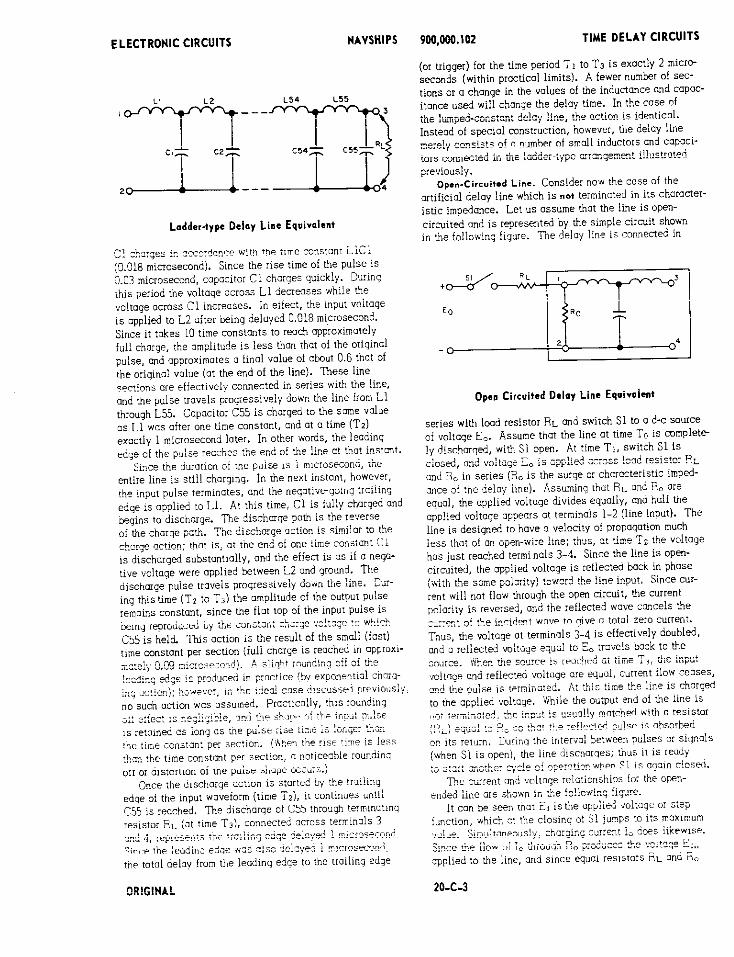
A detailed analysis of the operation of a typical distri- buted-constant type of delay line (chosen ior ease of ex- planation) using actual values follows. As constructed, the line consists of very fine wire (No.40 AWG. 0.0031 ~nch in diameter), wound on a plastic core. This continuously wound coil has a diameter of approximately 3/16 inch, md contains 109 turns per centimeter of lenqth to provide o rated inductance o f 20 microhenries per centimeter. An insulating sleeve is placed over the coil, and an external copper braid i s used to provide o shielded outer conductor, which forms a capacitance of 16.5 picofarads per centi- meter with the coil. The measuredtime deloyis 0.018 microsecond per centimeter. To produce the l-microsecond time delay mentioned in the previous discussion, a 55 centimeter length of this line i s required. Therefore, we can consider the line to be made up of 55 sections ( I cm Ions), formins onequivalent ladder-type line a s illustrated . ~ . ~
in the accompanying figure. Although in the previous discussion an ideal pulse was
assumed, with zero rise time, a practical square input pulse hos o finite rise time. A value oi 0.03 microsecond for 3 1-mic:osemnd pulse i s :e?resentct:w 31 ~ t : 3 1 iise md 1311 tme 13ler3nces er.colrrere1 in p:anice. !,?a r t l i
pulse i s applied to the input of the line at time T i , temi- n d s 1 and 2, coil L1 provides o countm enif which slows down or opposes the passage of current flow through it. The current through L1 i s the charging current for capaci- tar C1 and the remainder of the line sections. Capacitor
20-C-2

ELECTRONIC CIRCUITS NAVSHIPS 9M),W0.102 TIME DELAY CIRCUITS
Current and Voltage Relqtionrhipr of Open-Circuited Line
form o voltage divider ocross the input, the voltage E,, is reduced to half of Ei, remains at thisvalue during the time of two deloy periods, and then returns to the source volue when the line i s fully charged and no further charg- ing current flows. At the output of the line the step funr tion E, rises to oneholf maximum value after one delay period, md then to full volue at the end of the remaining delay period. With the line fully charged ot the end of two delay periods, it remains at the original applied volue of Ei until Sl is opened: the line then discharges. In proc- tice, this i s usually accomplished through the grid resistor of the stage which it triggers (the delay line i s connected in parallel across the grid resistor in place of the conven- tional grid capacitorl. Thus we can soy that an open-ended delay line operates on a step function of voltage to produce a pulse of current equal in duration to twice the length of the line. ?he pulse across the characteristic impedance in series with the line has onchalf the amplitude of the step function.
Short-Circuitod Line. Consider now the case of an artificial delay line which i s terminated by o short circuit ot terminals 3-4, as shown in the accompanying figure.
Short-circuited Delay Line Equivalent
The illustration i s identical to the illustration of the open- circuited line shown previously, except that the output i s short-circuited. At time T I when S1 i s closed, the applied voltage divides equclh between RL and R,. At time T 2
the voltage reaches terminals 3-4 and i s invened in polarity by the short circuit and sent back toword the source. Simultnneously, h e current i s reflected back in phase with the source wove. Therefore, the current doubles while the voltages of the reflected and incident wave cancel to produce zero voltage. The current wove then travels bock to the source in coincidence with the opposite- ly polarized reflected voltage. #hen the source is reoched ot time T3, the input voltage across R, is completely canceled a d i s therefore zero, while the current i s double the starting value. In effect, the input to the line o t this time i s short-circuited also, and the line i s completely discharge3, reody for mother cycle of operation.
The current md voltage relotionships for the short- circuited line ate s h o w in the following figure. In this case, I, is the step function, which ot the closing of SI jumps to its maximum volue. Simultaneously, the applied voltoge, EL, does likewise. Because of voltogedivider action, E, (the voltage across R,) i s hdf the source value. or Ed. It remains at this volue for the time of two delay periods, and returns to zero when the out-of-phase reflected pulse reaches the input and produces cancellation. Volt-
Current and Voltage Relationships of Shorted Line
age EL across RL i s produced at hali omplitude since it i s equal to the input voltage across Ro; it remains at this volue for two deloy periods and then rises to the source volue at the termination of the pulse. The voltage ere, i s the reflected voltage, which does not exist until time T z ; it is neqotive sad equal in omplitude to E,. Once started by the reflection, it continues to flow back to the source until time T3, when it reaches the start (TI) and terminotes output pulse Eo. Output pulse E, originates at time TI a t half the amplitude of source voltow El, continues for the time o! two deloy periods, ond i s then terminated.
In the case of the shorted line, then, we can say that it operates on a step function of current to produce a pulse of volmgs equol in durotion to twice the length 01 the line. The voltage produced has holf the omplitude of the step of current multiplied by the characteristic impedance. Thus, there i s complete duality between opm lines charged from a constant-voltage source, ond short-circuited lines harged
ORIGINAL

ELECTRONIC CIRCUITS NAVSHIPS
from a cmstantsurrent source. ?he choice of the method deoends uwn the characteristics of the switch used to produce the step function. A thyratron switch has an im- pedance of less than 10 ohms and,therefore, effenively constitutes o constant voltage source. A pentode switch, on the other hand, may have M impedance of a meqohm when closed, and yet switch appreciable currents. Wile the discursioo n b v e has assumed ideal step function operation, in actual practice there i s M effect produced by the steepness of the grid pulse and stray capacitance, which determine the dove of the leadins edqe of the pulse. Line attenuation olso produces phase distortion; the characteristic im~edance of the line and the iine resistance produce a slope on the trailing edge of the pulse, md ?c:;~ize the !!ctril nmnlitude oi the pulse. Accidental resonances in the iine con cause oscillation following b t h edges of the pulse. Llnterminated open or shorted lines will tend to produce another reflection at the Input end, and cause a !o!lowinq pulse of lower omplihide until attenuated by the losses in &e line [this i s effectively an oscil!atory condition). The following figure shows some typical wave- forms taken with different line terminations, and i s indica- tive of typicol responses of artificial delay lines. Tne pulse length i s 1-minosecond, and the delay time i s olso 1
Typical Dcloy Waveforms fot Voriorr Terminations
nicrosecond. Part A of tL,e "ure shows both input (em) . . an: ;;t7;t !e,! wnvetnrms with L;e delay i i x ni~pi.r:y m~ " i i],e uiF;: 2-6 f ? ~ . tri2p.li. Port D sho,,xs
W0,000.102 TIME DELAY CIRCUITS
the input woveiorm with the input properly terminated and the output short-circuited. Note hot between times Ti and Tz the output pulse i s effectively cancelled by the negative inverted pulse, whose lwding edge appears at Tz and lasts until T3. Since the amplitude of the inverted pulse is not exoc.2~ qun! to thnt o! the input pulse, slight pips oppear at T4 and Ts, even though the input i s properly ircinirrated. Pcrt C shows o partially shorted line, that is, with the load only oncholf the value cf the line characteris tic impedonce, and with the input properly terminated. In this case, since the mismatch i s oppmximotely 50% there i s o refleaion of approximately 1/4th the amplitude, with the remainder being obsorhed. Note thot because the r e sistance or impedwce i s lower thm that of the line, the signal i s inverted as with the short-circuited line. Port D shows n more nwriy mui~i~i.2 ii.c&'.;c, a! ~ h n c ! 20% mis- match. While the reflection i s still invened, bemuse tne impedance of the laod i s lower than that oi the line, its omlitude i s very small. Port E shows tine input waveform with the input and output &ti! piirper!) t c x i n ~ l d . In 6i:; case the output is absorbed by the proper termination, ond no reflection occurs: hence, the input pulse stands alone. Part F shows the condition ior o 50% mismatch, with the load impedance twice the line impedance. In this case the reflected pulse is of the some poiarity a s the input, acting a s an open line, since the load impedance i s higher than the surge impedance of the ilne. Tne ompiitude i s not half of the input, but opproximotely one-quarter, exactly a s in the opposite case of 9% mismatch shown in port C. Pan G shows the waveform at the input with the output zpm-cirmited and with the input pmperly terminated. In this case the open iine meaiei 2 xmp!ete reflection, which i s not quite equal in amplitude to the input signal becouse oi line attmtuauon: therefore, there i s a slight reflection, causing the minor pips at TI and T5, even though the input i s properly terminated. T i e final case i s witb. the output short-circuited and the input terminated in a lower impedance than tho1 of the iine. Pait H ?haws the input woveform !or this wse. Since the line i s shorted, the reilected pulse i s inverted, and, since it i s improperly terminated at the in- put, reflection occurs, with each succeeding waveform being further reduced in amplitude. This i s equivalent to on oscillatory condition or rm undwped transient response.
Pull.-Forming Line. !n t i e two preceding cases of open ond shorted delay lines, the action wos considered with the 1:ne discharged and a pulse applied. In the third 3 a m e invo!v:n$ rhe use of a de!w,.!ine, the line :s firs? chnrged !o o specific level, i s then dismnnecte6 ;r? ^;sc+.arged. an6 finoily !oms o pulse with steep ieod- ing and wailing edges and with o time duration q u a i to rne . . :i-e. The i j icam~r.vino fiqure shows o simple schematic ~.;ui.ra:ei,t o! s-cL 5 p d s n f o n i n n circuit. A s i k ~ ~ r n , L$e !inc is connected ihiouyh El, Sl, on@ RL to the 4.1 source voltage, E,. Swltch Si is hnked r , ~ L , . u -i--,-c!'.. A,.--.., wiih Si su ii,at flh-i. S: ic r l o s d $2 is open. and vlce versa. ' h e lire i s not terminated, but rather i s operrcir- cuited. Ar Lime To j-itch S! i s zlose.1 no4 the line i s per- mined to charge until i l reaches a steady-state cor,&tiar *it+ the line chorged to voltage E,. (This charge mnsists !!,:,i;iy ~i ci^l::n~t~ric e n ~ i n ~ ,. %!me6 :n the copocitors.i At .~-. T . s:v:!ch 52 !s dnbvci: i j~enir ; . ~ C!, c?6 !h.e l:v riiiin-
ORIGINAL 764.978 0-65 - 3 4
ELECTRONIC CIRCUITS NAVSHlPS 900,000.102 TIME DELAY CIRCUITS
Line Dlrcharge Eqrivalent Circuit
charges through RL. The discharge current through Rr produces voltage EL, which i s the desired output voltage. The flow of currmt through RL produces a voltage wave which travels b m terminals 1-2 of the delay line toward open end 3-4. Since the l w d resistor i s placed in series with the line and the line i s now acting a s the source of voltage, this voltage divides between the characteristic im- pedance of the line and RL, which i s of the same resistance. Therefore, the initial discharge voltage i s half of the value to which the line i s charqed. Because the flow of currmt i s now reversed, the polarity of the voltage wove i s opposite that to which the line was initiallv doraed. As this in- duced wave trovels down the line,'it &cels out the original charge by one-half the maximum charae voltaae. Thus, the discharge current which Uows through RL i s Gual to Ed2Ro. Whm the wave rmches terminals 3-4, reflection occurs. The reflected wave i s now of the same polarity a s the induced voltage wave and, since current cannot flow in an open circuit, the voltoge doubles, becoming equal to E.. The polarity of the discharge (induced) wove i s opposite the original polarity of E,: thus both voltages are equal and ancel . Since the current mnnot flow further, it i s inverted in polority ond travels back to the source, wiping out the current wave a s it travels. When the reflect- ed wave reaches the input terminals, all the elenrostatic energy stored in the line i s mmpletely discharged, and neither current nor voltoqe exists anywhere dona the line. Switch S2 i s then openedand S1 i s dosed, starting a new cycle of operation. In this instance the discharge of the line has resulted in a rectangular pulse with a duration equal to twice the deloy time.
Current and voltage relationships for the charge and discharge of the delay line are shown in the following figure. At time To, when Sl is closed and S2 i s open, the source voltoge i s applied to the line through charging resistor R I in series with Ro and Rr. In the ahsence of R L h e line would hove half the source voltage applied. However, RI i s o largevalue resistor (where the PR loss in this resis- tance i s undesirable o choke i s used instead), and only a smoll voltage i s applied to the line. The initiol voltage i s reflected again and again (as shown in part A) until the line i s finally charged up to the source voltage (assuming that the period of time between To and TI i s suifi- cient). At time T I , when switch Sl i s open and S2 is closed, the discharge commences and the chorge volt- aqe immediately drops to half the maximum value. The
Current and Voltage Relationrhipr for Discharge Line
line voltoge remains at this value until time Tz i s reached, when the discharge ceases. Thus, from port B of the figure it con be seen thot between T I and T? the linedischorges at o constant current with a volt- age equal to one-holf the initial charge voltage.
The ladder-type LC networks used for the delay lines discussed previously are sometimes replaced by o more sophisticated type of line which uses a two-terminal series arrangement instead of the four-terminal parallel arrangement, as shown in the following simplified schematic. In this arrangement the two sections hove different volues of L and C. This type of construction is similar to the m-derived filter. The theory of operation i s identical to thot of the ladder-tvw of delov line: the . . different construction merely provides equivalent or better pulse response chorocteristics with fewer sections.
Two-Terminal Delay Network
An artificial deloy line used with a typical pulse generator to produce an output pulse equal to the delay time is shown in the following schematic. In this opplicotion o step function of voltage is ow plied to a delay line (which is connected to a tube element) ot the same time the input pulse (step func- tion) i s applied to another tube element. The in- verted and delayed pulse stops circuit action ot the end of the delay period. Transformer T I hos two
ORIGINAL

ELECTRONIC CIRCUITS NAVSHIPS
7 r
Typical Pulse Genervtor
secondary windings, 72 and 73. ':;inding T3 is con- nect& to the bias source on6 the contro! y i 3 of the tube. ',:!hen n positi-ue input oulse is oypiied tc the primow, the induced pulse in !he secondary of T3 causes the tube to conduct. Secondary T2 i s con- nected onoss the delay line. !o:xing ; sharted line, with the opposite end properlv terminated bv R l and - - . connectd-to the suppressor grid. In the okence of a pulse and for the initial deloy period, the sup
~ ~
pressor is essentially at ground potential, being connected fhmuqb the ,wildinl to -j:c;ri?. '!,%EL :+:e il . i L i,i -- pu:se i s ilppiled to primary Ti, o positive
pulse travels along the line, is inverted, and 02- ?ears as 3 neqatlve stit-of! jote at the suppressor grid. Conduct~on occurs only during the time delly peno?. 3y tube x ~ m n :be p!lte cxrent pulsd pic- duces on inversion of the positi,,e input pulse, ~ n d provider 0 nrqative O U I D U ~ pulse onoss EL; w h r h rjp pears a1 C,; this pulse i s equal to the deloy perid. Bemuse of the numerous voriations in circuity no
. " I L - ' c nu, uc ~.,mdr to cover any other proctlca! clr-
cuils. Tne operation of t i e various circuits i s es- sentioliy the same, with the o~tput 01 1k.e delay line c~"tm!!i?: !he ci:cli: :̂:;:I.
FAILURE ANALYSIS. Smce ihr O:tjj:c::) dtlcy i;zp ,-,-,r:;<:: ,-,: in;:,:-
tors ond capacitors, o s:wie ~ P S ~ S : W C P nr ecctrs~i.; -Lick * i l l ,jrirrllilne wrl+n-i I!na i~ nnnl -- -i-:+ ~~ ~~~
circuited. Hasicolly, the line either works or it coes net amk. !! i t -,-,; ;b.- -,,: ~~. 1, ~ ~. '" *:... ."" :oztlc!!e? ::r:Ait ; : 2 . . ~ 5 ~ " -"!be "! L A C <"ronq *rJtP
ond s i o ~ . (! is ce:-p:-ilrl I- -kc-;;; .I,; , circuit waveforms with. ,an nsc ! l l n i c~yz . !Ic,,nll:, !be
., . . A e , " , , , < - " : . " * " 7 , ~ 4 . - . - ~ , "-.-, ..... ... -,,..,, ." ji.; L L ~ L U L u. , iuur, r r t
which event the plate ..h':veio:n.. bei;.; an i,cv.crtsi: m,l ~ i i l p l i f ~ d ftp:iiu, ir;uy h. ubserved to ovoid shunonq the ilne wltr ire oscilloscaae inout. !t t ie ri-c line 1s SISW, it may be beimse !he iry':t y d s e ;::::i 'x :;c ..;; -,,,:-; 'i i. ,,., l, tLr il:!= !:!..!:c:~̂ cc : C E:oE:n:.; ir;;;;;ii ,," , . . . . .,r,n, l "? mp "I rce .!:is: 5!^3e5 cxcc5;ivc:;. :hi
YUU,CW. IOZ TIME DELAY CIRCUITS
reslstonce in ti!e line isexcessive. Uormoliy, a sligk,t slope is expected since the line resistance con never be zero. L'sunlly, the line resistance will oiso p l x e o slight tail on the pulse in short-c~rcuited lines. Adding additional sectlons wliitend to sharoen therise and fail time, but will ~ l i o mokc the delay :me lsnjei. Therefore. in such case, the told inductonce per section will necessarily h x e to be reduced. In proct~ce. n deiect~ve deloy line is ilsuolly replaced with o new one. Othewise it will be neccssorf to occlir~ltelv meiisure the individual components ininductance ondcopocitonce bridges to determine ,whether th,ey crrdefectlve. 'Xh11t lirsrrtiot~ or removal of a comooner~t or secacr mn.y tenwr-iiib: re-!nie tne line to proper operating ronditior, this wi!! be ;.G
assurance th?t other c?rnnon~v.t; rnie ̂ -t ?FLI !,:.T;~'
Ly t k ~ . cause ~i Lie P I B V ~ D U ~ lailuie, and will themselves soon fai! zn.! cnuse 2 siri!ar csciition. Tai:;ie of the assxla tsd !me cnd arctiit 1s more c;n,mon than dpioy i~neia~iure . .Ie?!lce t n e ?l:c?el.? I l t e s,!!!. 2 k:cr;:. good one and ckck thevalues a! theresistors in the cir- cuit. Failure of the terminating resistor is usually indicated by the presence of additional ref!ections sr by a;; sscillotory condition.
ORIGINAL
