oxygen effect on structural and optical properties … · oxygen effect on structural and optical...
TRANSCRIPT
DOI: http://dx.doi.org/10.1590/1980-5373-MR-2016-0478Materials Research. 2017; 20(3): 607-612 © 2017
Oxygen Effect on Structural and Optical Properties of ZnO Thin Films Deposited by RF Magnetron Sputtering
Bassam Abdallaha, Abdul Kader Jazmatia*, Raeda Refaaia
Received: June 27, 2016; Revised: January 22, 2017; Accepted: February 18, 2017
ZnO thin films with wurtzite structure have been grown on Si (100) and glass substrates using radio frequency (rf) magnetron sputtering at room temperature. The ZnO thin films have been characterised by XRD. The (002) orientation is observed at zero Oxygen flow after the (100) developed with increasing oxygen ratio. Usually, this orientation (100) is difficult to obtain. The thickness of ZnO films was confirmed by cross-section SEM, and their stoichiometry was measured by Energy Dispersive X-ray Spectroscopy (EDX) and Rutherford backscattering spectroscopy (RBS). The optical band gaps have been determined using UV spectra and found to be varied from 3.24 to 3.29 eV as a function of the oxygen ratio. Moreover, photoluminescence (PL) spectra showed more defects at higher oxygen flow. The crystalline quality of the deposited film degrades with oxygen enhancements.
Keywords: Thin films, zinc oxide, deposition rate, structural characteristics, optical properties
* e-mail: [email protected]
1. IntroductionZinc oxide (ZnO) is a promising wide band gap
semiconductors due to its low electrical resistivity, high conductivity, environmental stability, nontoxicity and transparency, as well as being inexpensive. ZnO is a direct band gap semiconductor of energy Eg = 3.37 eV, and exciton binding energy of ~ 60 meV at room temperature. So, it can be used as a transparent electrode in solar cells manufacturing1, in liquid crystal display (LCD)2 and in light emitting diode (LED)3. In addition, ZnO is useful in many potential applications and can be exploited as a thin film transistor (TFT)4,5, and surge protection element in electronic circuitry6-8, UV photodetector9, transparent conductor10, piezoelectric transducer and surface acoustic wave device11. Recently, semiconducting metal oxide materials (such as ZnO) have used as gas sensors, since they develop electrical characteristics influenced by the composition of the surrounding gas ambience12. Different processes are used to prepare ZnO thin film synthesis such as Pulsed Laser Deposition (PLD)13,14, spray pyrolysis15, chemical vapour deposition CVD16, and electrochemical deposition technique (ECD) is used for the synthesis of semiconductors oxides at low temperature17,18. Magnetron sputtering19,20 is widely used in the semiconductor technology manufacturing, because of producing high quality ZnO films with controlled thickness and morphology21. Plasma and deposition parameters such as substrate temperature, RF power and oxygen partial pressure influence on the physical (structural and optical) properties of oxide thin films22, where the good quality thin films were obtained with the (002) orientation at 400°C temperature in the presence of 50% of oxygen amount.
Changing the orientations is very important during the growth of nanowires23, it was found that the wires on the ZnO film with (002) texture grow perpendicular to the surface of the film, and the wires on the film with (100) texture grow in the plane of the substrate.
In this work, ZnO films have been deposited by vacuum RF sputtering method. The crystallographic properties of the films were characterized by XRD. The RBS analysis method was employed to reveal information about the composition of the films, and PL and UV spectra have been obtained to study the optical properties of the films. The effect of oxygen partial pressure on the optical and structural of the grown films was investigated as well.
2. Experimental Procedure
RF magnetron sputtering using a PLASSYS-MP600S deposition system has been used to produce zinc oxide films at room temperature (RT). The films were deposited on silicon Si (100) and glass substrates. The zinc oxide target’s (purity 99.99%) diameter was 15 cm with a 6 cm distance between the cathode and the substrate holder. The vacuum in the deposition chamber was about 2 × 10⁻⁷ Torr21. The deposition rate was monitored in situ by a quartz crystal monitor and measured ex situ by means of a scanning electron microscope (SEM) TSCAN Vega II XMU (Czech Republic) operated at 30 kV equipped with EDX, where the films thickness was 150 nm. All the deposition conditions are summarised in table 1.
The crystallographic properties of the films have been analysed by XRD Stoe transmission X-ray diffractometer Stadi P (Germany) using the Cu Kα (with λ = 0.15405 nm)
a Atomic Energy Commission, Department of Physics, P. O. Box 6091, Damascus, Syria
Abdallah et al.608 Materials Research
Table 1: Deposition conditions
O2 flow (sccm) 0 4 8 12 15 18 20
Ar flow (sccm) 20 16 12 8 6 3 0
Oxygen percent(%) O2/(Ar+O2) 0% 20% 40% 60% 70% 85% 100%
RF Power 600 W
Total Pressure 3 mTorr
radiation in a linear position sensitive detector for θ–2θ scan configuration.
In addition, the RBS analysis has been conducted at the 3MV HVEE™ tandem accelerator at the Atomic Energy Commission of Syria (AECS) using a 4He+ beam of 2.0 MeV, and the RBS spectra were treated using the computer code SIMNRA24. The morphology was obtained by SEM measurements, and the atomic composition and stoichiometry of the ZnO films were determined by RBS. The optical characteristics have been examined using the UV-vis Shimadzu UV-310PC Spectrophotometer to measure the transmittance of the elaborated films, and a 325 nm wavelength of a He-Cd laser, a 1m Spex monochromator and a multialkali photomultiplier were used for the photoluminescence (PL) measurements at RT.
3. Results and Discussion
3.1 Deposition rate and composition measurement
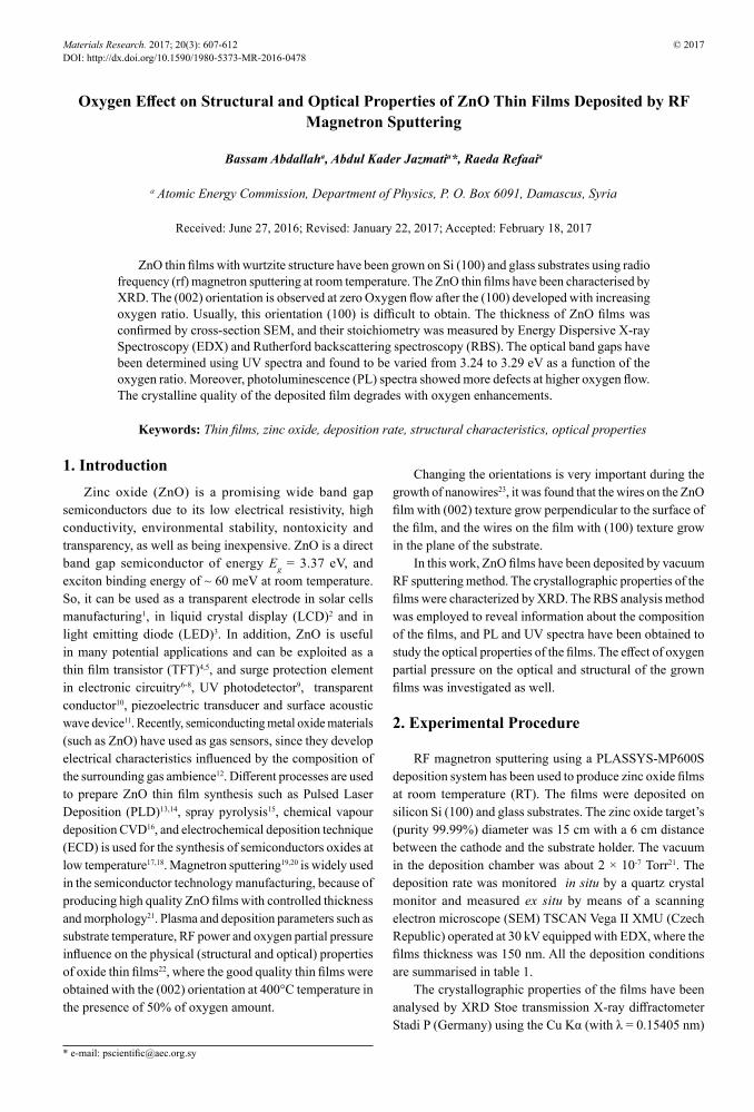
The evolution of the deposition rate versus oxygen flow ranging from 0 to 20 sccm was elucidated in Figure (1-a). The deposition rate decreased from 50 to 22 nm/min as a function of the concentration of oxygen (0 to 100%) 0 sccm-20 sccm.
The increasing of the oxygen percentage induces a decrease of the deposition rate due to a decreasing of sticking coefficient22. On the other hand the increase of the oxygen gas flow would decrease the argon partial pressure and subsequently decrease bombarded argon ions towards targets25,26. Figure (1-b) shows SEM cross section for ZnO/Si film and equals to 150 nm thickness.
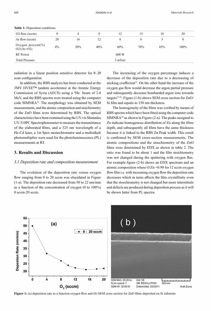
The homogeneity of the films was verified by means of RBS spectra which have been fitted using the computer code SIMNRA24 as shown in Figure (2-a). The peaks assigned to Zn indicate homogenous distribution of Zn along the films depth, and subsequently all films have the same thickness because it is linked to the RBS Zn Peak width. This result is confirmed by SEM cross-section measurements. The atomic compositions and the stoechiometry of the ZnO films were determined by EDX as shown in table 2. The ratio was found to be about 1 and the film stoichiometry was not changed during the sputtering with oxygen flux. For example figure (2-b) shows an EDX spectrum and an atomic composition where O/Zn =0.99 for 12 sccm oxygen flow film i.e. with increasing oxygen flow the deposition rate decreases which in turns affects the film crystallinity even that the stoechiometry is not changed but more interstitials and defects are produced during deposition process as it will be shown latter from PL spectra.
Figure 1: (a) deposition rate as a function oxygen flow and (b) SEM cross section for ZnO films deposited on Si substrate
609Oxygen Effect on Structural and Optical Properties of ZnO Thin Films Deposited by RF Magnetron Sputtering
Figure 2: (a) RBS spectra of ZnO/Si at different oxygen flow and (b) Atomic composition by EDX characterization for ZnO/Si film at 12 sccm
Table 2: Atomic percentage for ZnO film for different oxygen flow
Atomic percentage [O] [Zn] [O]/[Zn]
0 sccm 48.27 51.73 0.93
4 sccm 49.70 50.30 0.99
8 sccm 50.15 49.85 1.01
12 sccm 49.74 50.26 0.99
15 sccm 49.24 50.76 0.97
18 sccm 48.70 51.30 0.95
20 sccm 50.79 49.21 1.03
3.2 Structural characterization
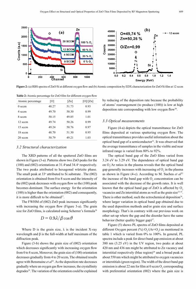
The XRD patterns of all the sputtered ZnO films are shown in Figure (3-a). Patterns show two ZnO peaks for the (100) and (002) orientations at 31.4oand 34.4o respectively. The two peaks attributed to hexagonal würtzite phase. The small peak at 33o attributed to Si substrate . The (002) orientation is obtained from 0 to 8 sccm and the intensity of the (002) peak decreases with oxygen flow so the (100) peak becomes dominant. The surface energy for the orientation (100) is higher than the orientation (002) and consequently, it is more difficult to be obtained27.
The FWHM of (002) ZnO peak increases significantly with increasing the oxygen flow (Figure 3-a). The grain size for ZnO films, is calculated using Scherrer’s formula28
. / cosD 0 9m b i=
Where D is the grain size, λ is the incident X-ray wavelength and β is the full-width at half maximum of the diffraction peak.
Figure (3-b) shows the grain size of (002) orientation which decreases significantly with increasing oxygen flow from 0 to 8 sccm, Moreover, the grain size of (100) orientation decreases gradually from 4 to 20 sccm. The obtained results agree with Bensmaine et al22. As the deposition rate decreases gradually where an oxygen gas flow increases, the crystallinity degrades29. The variation of the orientation could be explained
by reducing of the deposition rate because the probability of atoms’ rearrangement (to produce (100)) is low at high deposition rate corresponding with low oxygen flow30.
3.3 Optical measurements
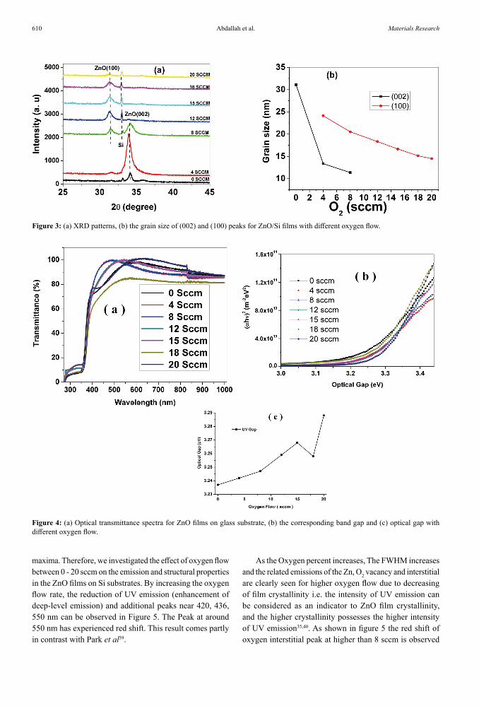
Figure (4-a) depicts the optical transmittance for ZnO films deposited at various sputtering oxygen flow. The optical transmittance provides useful information about the optical band gap of a semiconductor31. It was observed that the average transmittance of samples in the visible and near infrared range is varied from 80% to 92%.
The optical band gap of the ZnO films varied from 3.24 eV to 3.29 eV. The dependence of optical band gap on O2/Ar ratios in the plasma reveals that the optical band gap generally increases with increasing of O2 in the plasma as shown in Figure (4-c). According to M. Suchea et al32 the increase of the band gap with O2 concentration can be associated with the decrease of the growth rates. It is well known that the optical band gap of ZnO is affected by O2 vacancies and Zn interstitial atoms as well as the grain size33-35. There is other method, such the ectrochemical deposition36, where larger variation in optical band gap obtained due to the used deposition methods and/or grain size and surface morphology. That’s in contrary with our previous work on other set-up where the gap and the disorder have the same behavior (better quality bigger gap)37.
Figure (5) shows PL spectra of ZnO films deposited at different Oxygen percent (%) O2/(Ar+O2) as mentioned in table 1 which is varied from 0% to 100%. In general, PL spectra include a peak for direct band gap emission at about 380 nm (3.25 eV) in the UV region, two peaks at about 420 nm and 436 nm might be attributed to Zn vacancy and interstitial respectively (blue region)38 and a broad peak at about 550 nm which might be attributed to oxygen vacancies or interstitials (green region). The width of the direct band gap emission is about 22 nm for film at 0 sccm O2 corresponding with preferential orientation (002) where the gain size is
Abdallah et al.610 Materials Research
Figure 3: (a) XRD patterns, (b) the grain size of (002) and (100) peaks for ZnO/Si films with different oxygen flow.
Figure 4: (a) Optical transmittance spectra for ZnO films on glass substrate, (b) the corresponding band gap and (c) optical gap with different oxygen flow.
maxima. Therefore, we investigated the effect of oxygen flow between 0 - 20 sccm on the emission and structural properties in the ZnO films on Si substrates. By increasing the oxygen flow rate, the reduction of UV emission (enhancement of deep-level emission) and additional peaks near 420, 436, 550 nm can be observed in Figure 5. The Peak at around 550 nm has experienced red shift. This result comes partly in contrast with Park et al39.
As the Oxygen percent increases, The FWHM increases and the related emissions of the Zn, O2 vacancy and interstitial are clearly seen for higher oxygen flow due to decreasing of film crystallinity i.e. the intensity of UV emission can be considered as an indicator to ZnO film crystallinity, and the higher crystallinity possesses the higher intensity of UV emission35,40. As shown in figure 5 the red shift of oxygen interstitial peak at higher than 8 sccm is observed

611Oxygen Effect on Structural and Optical Properties of ZnO Thin Films Deposited by RF Magnetron Sputtering
Figure 5: PL spectra of ZnO thin films on Si substrate versus wavelength with different oxygen flow.
simultaneously with an orientation changement from (002) to (100) which is consistent with the XRD study.
4. Conclusions
ZnO thin films have been grown on Si (100) and glass substrates using radio frequency (rf) magnetron from ZnO target. The X-ray diffraction patterns have shown (002) orientation with the best quality for ZnO films grown at zero oxygen flow. By increasing the oxygen ratio, the deposition rate decreases and subsequently crystalline quality degrades as it related to the decrease of the grain size, Photoluminescence spectra indicated more Zn, O vacancy and interstitials at higher oxygen flow and the Peak at around 550 nm has experienced red shift. Optical band gap of the films has varied from 3.24 to 3.29 eV as a function of the oxygen percentage.
5. Acknowledgement
Authors would like to thank Prof. I. Othman, the Director General of AECS for support, prof. M. Zidan for beneficial discussion, F. Nounou for films preparation and M. Alsabagh for PL measurements.
6. References
1. Wang ZA, Chu JB, Zhu HB, Sun Z, Chen YW, Huang SM. Growth of ZnO:Al films by RF sputtering at room temperature for solar cell applications. Solid State Electronics. 2009;53(11):1149-1153.
2. Oh BY, Jeong MC, Moon TH, Lee W, Myoung JM, Hwang JY, et al. Transparent conductive Al-doped ZnO films for liquid crystal displays. Journal of Applied Physics. 2006;99(12):124505-124509.
3. Pearton SJ, Lim WT, Wright JS, Tien LC, Kim HS, Norton DP, et al. ZnO and Related Materials for Sensors and Light-Emitting Diodes. Journal of Electronic Materials. 2008;37:1426-1432.
4. Hoffman RL, Norris BJ, Wager JF. ZnO-based transparent thin-film transistors. Applied Physics Letters. 2003;82(5):733-735.
5. Zhu J, Chen H, Saraf G, Duan Z, Lu Y, Hsu ST. ZnO TFT Devices Built on Glass Substrates. Journal of Electronic Materials. 2008;37(9):1237-1240.
6. Shinde VR, Gujar TP, Lokhande CD. Enhanced response of porous ZnO nanobeads towards LPG: effect of Pd sensitization. Sensors and Actuators B: Chemical. 2007;123(2):701-706.
7. Basu PK, Battacharyya P, Saha N, Saha H, Basu S. The superior performance of the electrochemically grown ZnO thin films as methane sensor. Sensors and Actuators B: Chemical. 2008;133(2):357-363.
8. Sahay PP, Nath RK. Al-doped ZnO thin films as methanol sensors. Sensors and Actuators B: Chemical. 2008;134(2):654-659.
9. Bi Z, Zhang JW, Bian XM, Wang D, Zhang X, Zhang WF, et al. A High-Performance Ultraviolet Photoconductive Detector Based on a ZnO Film Grown by RF Sputtering. Journal of Electronic Materials. 2008;37(5):760-763.
10. Kushiya K, Ohshita M, Hara I, Tanaka Y, Sang B, Nagoya Y, et al. Yield issues on the fabrication of 30 cm×30 cm-sized Cu(In,Ga)Se2-based thin-film modules. Solar Energy Materials and Solar Cells. 2003;75(1-2):171-178.
11. Fu YQ, Garcia-Gancedo L, Pang HF, Porro S, Gu YW, Luo JK, et al. Microfluidics based onZnO/nanocrystalline diamond surface acoustic wave devices. Biomicrofluidics. 2012;6(2):24105-2410511.
12. Shishiyanu ST, Shishiyanu TS, Lupan OI. Sensing characteristics of tin-doped ZnO thin films as NO2 gas sensor. Sensors and Actuators B: Chemical. 2005;107(1):379-386.
13. Kumar R, Kumar G, Umar A. Pulse laser deposited nanostructured ZnO thin films: a review. Journal of Nanoscience and Nanotechnology. 2014;14(2):1911-1930.
14. Vishnoi S, Kumar R, Singh BP. Effect of substrate on physical properties of pulse laser deposited ZnO thin films. Journal of Intense Pulsed Lasers and Applications in Advanced Physics. 2014;4(1):35-39.
15. Ayouchi R, Martin F, Leinen D, Ramos-Barrado JR. Growth of pure ZnO thin films prepared by chemical spray pyrolysis on silicon. Journal of Crystal Growth. 2003;247(3-4):497-504.
16. Ben-Yaacov T, Ive T, Van de Walle CG, Mishra UK, Speck JS, Denbaars SP. Properties of In-Doped ZnO Films Grown by Metalorganic Chemical Vapor Deposition on GaN(0001) Templates. Journal of Electronic Materials. 2010;39(5):608-611.
17. Khelladi MR, Mentar L, Beniaiche A, Makhloufi L, Azizi A. A study on electrodeposited zinc oxide nanostructures. Journal of Materials Science: Materials in Electronics. 2013;24(1):153-159.
18. Laidoudi S, Bioud AY, Azizi A, Schmerber G, Bartringer J, Barre S, et al. Growth and characterization of electrodeposited Cu2O thin films. Semiconductor Science and Technology. 2013;28:115005.
19. Gao W, Li Z. ZnO thin films produced by magnetron sputtering. Ceramics International. 2004;30(7):1155-1159.
20. Ismail A, Abdullah MJ. The structural and optical properties of ZnO thin films prepared at different RF sputtering power. Journal of King Saud University - Science. 2013;25(3):209-215.
Abdallah et al.612 Materials Research
21. Al-Khawaja S, Abdallah B, Abou Shaker S, Kakhia M. Thickness effect on stress, structural, electrical and sensing properties of (002) preferentially oriented undoped ZnO thin films. Composite Interfaces. 2015;22(3):221-231.
22. Bensmaine S, Le Brizoual L, Elmazria O, Assouar B, Benyoucef B. The effects of the deposition parameters of ZnO thins films on their structural properties. Journal of Electron Devices. 2007;5:104-109.
23. Hong JI, Bae J, Wang ZL, Snyder RL. Room-temperature, texture-controlled growth of ZnO thin films and their application for growing aligned ZnO nanowire arrays. Nanotechnology. 2009;20(8):085609.
24. Ismail IM, Abdallah B, Abou-Kharroub M, Mrad O. XPS and RBS investigation of TiNxOy films prepared by vacuum arc discharge. Nuclear Instruments and Methods in Physics Research Section B: Beam Interactions with Materials and Atoms. 2012;271:102-106.
25. Zhu H, Hüpkes J, Bunte E, Huang SM. Oxygen influence on sputtered high rate ZnO:Al films from dual rotatable ceramic targets. Applied Surface Science. 2010;256(14):4601-4605.
26. Sundaram KB, Khan A. Characterization and optimization of zinc oxide films by r.f. magnetron sputtering. Thin Solid Films.1997;295(1-2):87-91.
27. Fujimura N, Nishihara T, Goto S, Xu J, Ito T. Control of preferred orientation for ZnOx films: control of self-texture. Journal of Crystal Growth. 1993;130(1-2):269-279.
28. Scherrer P. Bestimmung der Grösse und der inneren Struktur von Kolloidteilchen mittels Röntgenstrahlen. Nachrichten von der Gesellschaft der Wissenschaften zu Göttingen, Mathematisch-Physikalische Klasse. 1918;1918:98-100.
29. Jiang YJ, Zhang DX, Cai HK, Tao K, Xue Y, Sui YP, et al. Influence of the gas flow of Argon and the distance between substrate and plasma on properties of Al-doped zinc oxide films. Journal of Physics: Conference Series. 2009;152(1):012030.
30. Lee JB, Park CK, Park JS. Physical Properties of RF-Sputtered ZnO Thin Films: Effects of Two-Step Deposition. Journal of the Korean Physical Society. 2007;50(4):1073-1078.
31. Abdallah B, Al-Khawaja S. Optical and Electrical Characterization of (002)-Preferentially Oriented n-ZnO/p-Si Heterostructure. Acta Physica Polonica A. 2015;128(3):283-288.
32. Suchea M, Christoulakis S, Katsarakis N, Kitsopoulos T, Kiriakidis G. Comparative study of zinc oxide and aluminum doped zinc oxide transparent thin films grown by direct current magnetron sputtering. Thin Solid Films. 2007;515(16):6562-6566.
33. Prathap P, Revathi N, Subbaiah YPV, Reddy KTR. Thickness effect on the microstructure, morphology and optoelectronic properties of ZnS films. Journal of Physics: Condensed Matter. 2007;20(3):035205.
34. Wang JM, Gao L. Wet chemical synthesis of ultralong and straight single-crystalline ZnO nanowires and their excellent UV emission properties. Journal of Materials Chemistry. 2003;13(10):2551-2254.
35. Wang YG, Lau SP, Lee HW, Yu SF, Tay BK, Zhang XH, et al. Photoluminescence study of ZnO films prepared by thermal oxidation of Zn metallic films in air. Journal of Applied Physics. 2003;94(1):354-358.
36. Mentar L, Baka O, Khelladi MR, Azizi A, Velumani S, Schmerber G, et al. Effect of nitrate concentration on the electrochemical growth and properties of ZnO nanostructures. Journal of Materials Science: Materials in Electronics. 2015;26(2):1217-1224.
37. Rahmane S, Djouadi MA, Aida MS, Barreau N, Abdallah B, Hadj Zoubir N. Power and pressure effects upon magnetron sputtered aluminum doped ZnO films properties. Thin Solid Films. 2010;519(1):5-10.
38. Wu KY, Fang QQ, Wang WN, Zhou C, Huang WJ, Li JG, et al. Influence of nitrogen on the defects and magnetism of ZnO:N thin films. Journal of Applied Physics. 2010;108(6):063530.
39. Park TE, Kim DC, Hong BH, Cho HH. Structural and Optical Properties of ZnO Thin Films Grown by RF Magnetron Sputtering on Si Substrates. Journal of the Korean Physical Society. 2004;45:S697-S700.
40. Ting CC. Structure, Morphology, and Optical Properties of the Compact, Vertically-Aligned ZnO Nanorod Thin Films by the Solution-Growth Technique. In: Yalçın O, ed. Nanorods. Rijeka: InTech; 2012. p. 33-50.